TECHNICAL FIELD
The present invention relates to a dimming device and a
display device capable of controlling the reflectance and
transmittance of light.
BACKGROUND ART
A phenomenon in which a metal thin film of yttrium (Y),
lanthanum (La), or the like bonds to hydrogen to change into
a hydride which can transmit visible light has been reported
(specification of US Patent No. 5635729, and Huibert and six
others, Nature, (U.K.), March 1996, vol. 380, pp.231-234).
Since this phenomenon is reversible, by adjusting the
hydrogen pressure in the atmosphere, it becomes possible to
cause the thin film to change between a metallic luster state
and a transparent state.
By changing the optical characteristics of the above
thin film so as to switch between a state exhibiting a
metallic luster and a transparent state, it becomes possible
to realize a dimming mirror which is capable of freely
adjusting the reflectance/transmittance of light. If a
dimming mirror is used as a windowpane of a building or an
automobile, for example, it becomes possible to shield
(reflect) or transmit sunlight as necessary.
Such a dimming mirror has, for example, a structure in
which a palladium layer is formed on a yttrium thin film.
The palladium has a function of preventing surface oxidation
of the yttrium thin film, and a function of causing hydrogen
molecules in the atmosphere to be efficiently changed into
hydrogen atoms so as to be supplied to yttrium. When yttrium
chemically bonds to hydrogen atoms, either YH2 or YH3 is
formed. While YH2 is a metal, YH3 is a semiconductor and has
a forbidden band width which is greater than the energy of
visible light, and therefore is transparent.
Moreover, since changes of states between YH2 YH3 occur
rapidly (about several seconds) even at room temperature, it
is possible to perform switching between a reflection
(metallic luster) state and a transparent state depending on
the amount of hydrogen content in the atmosphere.
As another material which is capable of such
transitioning between metallic luster transparent, a Mg2Ni
thin film is disclosed in Japan Society of Applied Physics,
2001 Spring Meeting, 31-a-ZS-14, for example.
The above conventional technique has a problem described
below.
Firstly, in order to change the optical state of a thin
film, it is necessary to expose the thin film to an hydrogen
atmosphere. Specifically, it is necessary to control the
amount of hydrogen (hydrogen partial pressure) in an
atmosphere gas which is in contact with the thin film.
Therefore, it is difficult to realize a practical dimming
device by using the aforementioned conventional constitution.
Secondly, in the dimming device according to the
conventional technique, a thin film containing a material
which is capable of transitioning between metallic luster
transparent (hereinafter referred to as "dimming material"),
e.g., yttrium, is used as a dimming layer. Such a dimming
device has the following problems.
The switching between the metallic luster and
transparent states in the dimming layer (thin film) occurs as
hydrogen ions permeate the dimming layer. However, even if
the hydrogen pressure in the atmosphere changes, reactions
with hydrogen ions may occur at the dimming layer surface,
but permeation of hydrogen ions into the thin film would be
difficult. Therefore, it is possible for some of the yttrium
atoms or molecules containing yttrium to remain unreacted.
As a result, it will be difficult to enlarge the difference
in reflectance between the metallic luster state and the
transparent state exhibited by the dimming layer. Moreover,
in order to use the dimming device for a broader range of
purposes, it would be necessary to reduce the time (switching
speed) required by the yttrium thin film (which is the
dimming layer) to transition between the metallic luster
state and the transparent state.
In order to enlarge the difference in reflectance
between the metallic luster state and the transparent state
and reduce switching speed, it might be conceivable to
improve the reaction efficiency of YH2 (or Y) YH3 in the
dimming layer, for example. However, in a conventional
constitution which uses a thin film as a dimming layer, there
are limits to improvement in the reaction efficiency.
Moreover, when applying a dimming device to a display
apparatus, it would generally be advantageous if the dimming
layer had a state in which light is diffuse-reflected.
However, the dimming layer in the dimming device according to
the conventional technique above mirror-reflects light in its
metallic luster state, and therefore is difficult to be
applied to a display apparatus.
Thirdly, in order to change the optical state of the
thin film according to the conventional technique above, it
is necessary to hydrogenate the material, contained in the
thin film, which is capable of transitioning between metallic
luster transparent, by exposing the thin film to a hydrogen
atmosphere. Specifically, it is necessary to control the
hydrogen amount (hydrogen partial pressure) in the atmosphere
gas which is in contact with the thin film. Since such
control of hydrogen amount is performed across the entire
surface of the thin film, the optical state of the entire
surface of the thin film changes.
Thus, conventional dimming devices are based on the
premise that they are to be applied to the purpose of
changing the optical state of the entire surface of the thin
film such as a dimming mirror, and applications to a display
apparatus have not been proposed. In order to realize an
application to a display apparatus, it would be necessary to
compartmentalize the thin film into a plurality of pixels,
and control the optical state of each pixel. However, it
would be difficult, and impractical, to control the hydrogen
amount in the atmosphere gas with respect to each pixel.
The present invention has been made in view of the above
circumstances, and it is intended to provide a dimming device
which is capable of allowing the state of a thin film to
transition between a metallic reflection state and a
transmitting state, without relying on a control of the
hydrogen amount (hydrogen partial pressure) in the atmosphere
gas. Moreover, it is intended to provide a dimming device
which comprises a dimming layer containing, in the form of
particles, a material that is capable of transitioning
between a metallic luster state and a transparent state, and
which is therefore able to switch the optical characteristics
of the dimming layer more rapidly and can be applied to a
broader range of purposes. Furthermore, it is intended to
provide a display device by utilizing the aforementioned
dimming device.
DISCLOSURE OF INVENTION
A dimming device according to the present invention is a
dimming device comprising a layered structure including a
first layer and a second layer, such that a light reflectance
of the first layer changes in response to an external
stimulation, characterized in that the first layer contains a
first material whose optical characteristics change in
accordance with a concentration of a specific element, and
the second layer contains a second material capable of
containing the specific element, the second material
releasing or absorbing the specific element in accordance
with the external stimulation. Thus, the above objective is
met.
In a preferred embodiment, the element is hydrogen, and
the first material is able to transition between a light
reflecting state and a light transmitting state in accordance
with a hydrogen concentration.
In a preferred embodiment, the first layer diffuse-reflects
light when the first material is in the light
reflecting state.
In a preferred embodiment, the first material is
particles.
It is preferable that a diameter of the particles is
equal to or greater than 350 nm and equal to or less than a
thickness of the first layer.
The first layer may contain colored particles having a
visible light absorbing ability, the particles being adsorbed
to the colored particles.
In a preferred embodiment, the second layer contains a
hydrogen storage material.
Preferably, operation occurs in a region where
respective hydrogen equilibrium pressure-composition
isotherms (PTC characteristic curves) of the first layer and
the second layer are substantially flat.
It is preferable that, in the region where the PTC
characteristic curves are substantially flat, hydrogen
equilibrium pressures of the first layer and the second layer
are about the same.
It is preferable that a range of hydrogen storage amount
of the second layer in the region where the PTC
characteristic curve is substantially flat encompasses a
range of hydrogen storage amount of the first layer in the
region where the PTC characteristic curve is substantially
flat.
In a preferred embodiment, the second material releases
or absorbs the specific element through exchanges of
electrons.
In a preferred embodiment, the second material releases
or absorbs the specific element in response to light
irradiation.
The second layer may contain a material having a
photocatalytic ability.
A pair of conductive layers for forming an electric
field for causing ions of the specific element to move from
the second material to the first material, or from the first
material to the second material may be comprised.
The first and second layer may be positioned between the
pair of conductive layers.
The first layer may have conductivity, and function as
one of the pair of conductive layers.
The second layer may have conductivity, and function as
one of the pair of conductive layers.
In a preferred embodiment, the second layer requires a
light transmitting ability.
In a preferred embodiment, at least one of an upper face
and a lower face of the first layer has bumps and dents, and
the first layer transitions between a state of diffuse-reflecting
light and a state of transmitting light, further
comprising a light absorbing layer for absorbing light having
been transmitted through the first layer.
In a preferred embodiment, the second layer requires a
visible light absorbing ability.
In a preferred embodiment, at least one of an upper face
and a lower face of the first layer has bumps and dents, and
the first layer transitions between a state of diffuse-reflecting
light and a state of transmitting light, and the
second layer is disposed opposite from a light incident face
of the first layer.
At least one of the first layer and the second layer may
have a multi-layer structure.
Another dimming device according to the present
invention is a dimming device comprising a dimming layer
whose light reflectance changes in response to an external
stimulation, characterized in that the dimming layer contains
a first material whose optical characteristics change in
accordance with a concentration of a specific element, the
first material being particles. Thus, the above objective is
met.
In a preferred embodiment, the first material is able to
transition between a light reflecting state and a light
transmitting state in accordance with the concentration of
the specific element.
In a preferred embodiment, the dimming layer diffuse-reflects
light when the first material is in the light
reflecting state.
It is preferable that a diameter of the particles is
equal to or greater than 350 nm and equal to or less than a
thickness of the dimming layer.
The dimming layer may contain colored particles having a
visible light absorbing ability, the particles being adsorbed
to the colored particles.
The specific element may be hydrogen.
A still another dimming device according to the present
invention is a dimming device comprising a dimming layer
whose light reflectance changes in response to an external
stimulation, characterized in that the dimming layer contains
a first material whose optical characteristics change in
accordance with a concentration of a specific element, and
contains a second material capable of containing the specific
element, the second material releasing or absorbing the
specific element in accordance with the external stimulation,
wherein the first material is particles. Thus, the above
objective is met.
A display device according to the present invention is a
display device including a plurality of pixels, each of the
plurality of pixels having: a first layer containing a first
material whose optical characteristics change in accordance
with a concentration of a specific element; a second layer
containing a second material capable of containing the
specific element, the second material releasing or absorbing
the specific element upon application of a voltage; and a
pair of electrodes for applying the voltage to the second
layer, characterized in that a light reflectance of the first
layer changes in response to the voltage. Thus, the above
objective is met.
In a preferred embodiment, the first material is able to
transition between a light reflecting state and a light
transmitting state in accordance with the concentration of
the specific element.
In a preferred embodiment, the first layer diffuse-reflects
light when the first material is in a light
reflecting state.
In a preferred embodiment, the first material is
particles.
In a preferred embodiment, at least one of an upper face
and a lower face of the first layer has bumps and dents.
In a preferred embodiment, the first layer further
contains colored particles, the first material being adsorbed
to the colored particles.
In a preferred embodiment, the first layer transitions
between a state of diffuse-reflecting light and a state of
transmitting light, and the second layer requires a light
transmitting ability, further comprising a light absorbing
layer for absorbing light having been transmitted through the
first layer and the second layer.
In a preferred embodiment, the first layer transitions
between a state of diffuse-reflecting light and a state of
transmitting light, the second layer having a visible light
absorbing ability, and the second layer is disposed opposite
from a light incident face of the first layer.
The second layer may be disposed on a light incident
side of the first layer, and function as a color filter.
The specific element may be hydrogen, and the second
layer may contain a hydrogen storage material.
It is preferable that the second material releases or
absorbs the specific element through exchanges of electrons.
The first layer may have conductivity, and function as
one of the pair of electrodes.
The display device according to the present invention
may be a reflection type display device.
The display device according to the present invention
may further comprise a backlight.
The first layer may transition between a state of
mirror-reflecting light and a state of transmitting light,
and a backlight may be further comprised.
BRIEF DESCRIPTION OF DRAWINGS
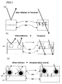
FIGS. 1(a) to (c) are cross-sectional views
schematically illustrating the dimming principle utilized in
the present invention.
FIGS. 2(a) to (c) are diagrams illustrating the
operation principles of a dimming device and a display device
according to the present invention.
FIG. 3 is a cross-sectional view showing first, ninth,
and twelfth embodiments of the dimming device according to
the present invention.
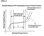
FIG. 4 is a graph showing a hydrogen equilibrium
pressure-composition isotherm (PTC characteristic curve) of a
dimming layer and a conversion layer.
FIGS. 5(a) and (b) are cross-sectional views showing a
dimming layer and a conversion layer of a second embodiment
of the dimming device according to the present invention.
FIGS. 5(a) to (c) are cross-sectional views showing a dimming
layer and a conversion layer of a tenth embodiment of the
dimming device according to the present invention.
FIGS. 6(a) and (b) are cross-sectional views showing
third and eleventh embodiments of the dimming device
according to the present invention.
FIG. 7 is a cross-sectional view showing a fourth
embodiment of the dimming device according to the present
invention.
FIG. 8 is a cross-sectional view showing the fourth
embodiment of the dimming device according to the present
invention.
FIG. 9 is a cross-sectional view showing a fifth
embodiment of the dimming device according to the present
invention.
FIG. 10 is a cross-sectional view showing a sixth
embodiment of the dimming device according to the present
invention.
FIG. 11 is a cross-sectional view showing a seventh
embodiment of the dimming device according to the present
invention.
FIG. 12 is a cross-sectional view showing an eighth
embodiment of the dimming device according to the present
invention.
FIGS. 13(a) and (b) are cross-sectional views showing a
thirteenth embodiment of the dimming device according to the
present invention.
FIG. 14 is a cross-sectional view showing a sixteenth
embodiment of the dimming device according to the present
invention.
FIG. 15 is a cross-sectional view showing the sixteenth
embodiment of the dimming device according to the present
invention.
FIG. 16 is a cross-sectional view showing a seventeenth
embodiment of the dimming device according to the present
invention.
FIG. 17 is a cross-sectional view showing an eighteenth
embodiment of the display device according to the present
invention.
FIG. 18 is a plan view showing the eighteenth embodiment
of the display device according to the present invention.
FIGS. 19(a) to (c) are cross-sectional views showing a
dimming layer and a conversion layer in the eighteenth
embodiment of the present invention.
FIG. 20 is a cross-sectional view showing a nineteenth
embodiment of the display device according to the present
invention.
FIGS. 21(a) to (c) are cross-sectional views showing a
dimming layer and a conversion layer in a nineteenth
embodiment of the present invention.
FIG. 22 is a cross-sectional view showing the nineteenth
embodiment of the display device according to the present
invention.
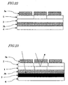
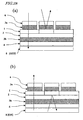
FIG. 23 is a cross-sectional view showing a twentieth
embodiment of the display device according to the present
invention.
FIG. 24 is a cross-sectional view showing a twenty-first
embodiment of the display device according to the present
invention.
FIG. 25 is a cross-sectional view showing a dimming
layer and a conversion layer in the twenty-first embodiment
of the present invention.
FIG. 26 is a cross-sectional view showing a twenty-second
embodiment of the display device according to the
present invention.
FIG. 27 is a cross-sectional view showing a twenty-third
embodiment of the display device according to the present
invention.
FIGS. 28(a) and (b) are cross-sectional views showing a
twenty-fourth embodiment of the display device according to
the present invention.
FIG. 29 is a cross-sectional view showing a twenty-fifth
embodiment of the display device according to the present
invention.
FIG. 30 is a cross-sectional view showing a twenty-fifth
embodiment of the display device according to the present
invention.
BEST MODE FOR CARRYING OUT THE INVENTION
First, the dimming principle which is utilized in
displaying by the display device according to the present
invention will be described. FIGS. 1(a) to (c) are schematic
cross-sectional views illustrating the dimming principle of
the display device according to the present invention.
A dimming layer M1 shown in FIG. 1(a) contains a dimming
material whose optical characteristics change in accordance
with the concentration of a specific element. Preferable
examples of the dimming material are Y, La, and Mg2Ni alloy
as described above, and the dimming layer 1 is a thin film of
such a dimming material, for example. Materials such as Y,
La, and Mg2Ni alloy undergo transitions between metal and
semiconductor (or insulator) states in accordance with
hydrogen concentration.
A conversion layer M2 contains a material capable of
containing a specific element such as hydrogen (which in the
present specification is referred to as a "conversion
material"). The conversion material releases or absorbs the
aforementioned specific element (e.g., hydrogen) in
accordance with an external stimulation, such as a charge
(electrons or holes) injection or light irradiation.
The dimming layer M1 and the conversion layer M2 shown
in FIG. 1(a) both have the ability to absorb/release
hydrogen, and have an electrical conductivity for being able
to move charges (electrons or holes) and ions.
Hereinafter, a mechanism where, responsive to
injection/release of a charge, hydrogen ions move from the
conversion layer M2 to the dimming layer M1, or from the
dimming layer M1 to the conversion layer M2, will be
described. A characteristic feature of this mechanism lies
in that ions of a specific element (hydrogen) which causes a
change in the optical characteristics of the dimming layer M1
are moved, not via an electrochemical reaction, but by way of
a charge movement.
FIG. 2(a) shows an initial state of the dimming layer M1
and the conversion layer M2 included in the structure of FIG.
1. In this initial state, an equilibrium state is
established between the dimming layer M1, which substantially
stores no hydrogen, and the conversion layer M2, which has
hydrogen stored in advance. Since the dimming layer M1 lacks
a sufficient concentration of hydrogen, the dimming layer M1
is in a metallic state, thus exhibiting metallic luster.
Next, as shown in FIG. 2(b), a negative potential is
applied to the dimming layer M1 side, while a positive
potential is applied to the conversion layer M2 side. At
this time, electrons are injected to the dimming layer M1
from a negative electrode (not shown), so that the dimming
layer M1 enters an electron-rich state. On the other hand,
holes are injected to (i.e., electrons are withdrawn from)
the conversion layer M2. The holes which have been injected
to the conversion layer M2 move inside the conversion layer
M2 toward the dimming layer M1. During such movements of the
holes, if further holes continue to be injected to the
conversion layer M2, the conversion layer M2 enters a hole-rich
state. As a result, the conversion layer M2 enters a
state where hydrogen ions are likely to be released, whereas
in the dimming layer M1, the amount of hydrogen ions which
are received from the conversion layer M2 and retained
therein increases.
Therefore, the hydrogen equilibrium state which existed
between the dimming layer M1 and the conversion layer M2 is
broken, so that the dimming layer M1 takes a state where more
hydrogen is likely to be retained, and thus the hydrogen ions
released from the conversion layer M2 will move to the
dimming layer M1. Thus, as shown in FIG. 2(c), a new
equilibrium state is established. In this state, the
hydrogen which has moved to the dimming layer M1 bonds to the
dimming material, whereby the dimming layer M1 becomes
transparent.
The above reaction can be described as M1 + M2(H)→M1(H)
+ M2. Herein, M1(H) and M2(H) respectively represent a state
where hydrogen is retained in the dimming layer M1 and a
state where hydrogen is retained in the conversion layer M2.
As is clear from the above explanation, only hydrogen
ion exchanges take place between the dimming layer M1 and the
conversion layer M2, and no other reactions involving ions
are taking place. Moreover, when the polarities of the
applied voltages are inverted from the state of FIG. 2(c), a
reaction will progress in the opposite direction, thus
returning to the original equilibrium state shown in FIG.
2(a). According to this mechanism, by applying an external
stimulation, e.g., voltage application, to the conversion
layer M2 containing a conversion material, the amount of
hydrogen content in the dimming layer M1 can be changed.
Therefore, a dimming device which utilizes this mechanism is
more practical than any dimming device according to the
conventional technique where it is necessary to control the
hydrogen partial pressure in the atmosphere.
Instead of the structure shown in FIG. 1(a), a layered
structure including a dimming layer M1 and a conversion layer
M2 as shown in FIG. 1(b) may be comprised. The dimming layer
M1 in FIG. 1(b) contains particles m1 (which may hereinafter
be referred to as "dimming particles") of a dimming material
whose optical characteristics change in accordance with the
concentration of a specific element. Preferable examples of
the dimming material are Y, La, and Mg2Ni alloy as described
above. The dimming layer M1 contains a binder resin, for
example, and the aforementioned dimming particles m1 are
dispersed within the binder resin. Moreover, the dimming
layer M1 also contains an electrolytic material (e.g., a
conductive polymer) for transporting hydrogen ions or
hydrogen from the conversion layer M2. The conversion layer
M2 is substantially similar to the conversion layer M2 which
has been described with reference to FIG. 1(a).
In the case where the structure shown in FIG. 1(b) is
used, in an initial state (FIG. 2(a)) of the dimming layer M1
and the conversion layer M2, the dimming layer M1 lacks a
sufficient concentration of hydrogen, and therefore each of
the dimming particles m1 dispersed in the dimming layer M1 is
in a metallic state and mirror-reflects light. Since the
dimming particles m1 cause the light entering the dimming
layer M1 to be reflected in random directions, the dimming
layer M1 as a whole diffuse-reflects the light. As a result,
white reflected light is obtained. When hydrogen ions move
to the dimming layer M1 and a new equilibrium state is
established (FIG. 2(c)), the hydrogen which has moved to the
dimming layer M1 bonds to the dimming particles m1, whereby
each dimming particle m1 becomes transparent.
Alternatively, a layered structure including a dimming
layer M1 and a conversion layer M2 shown in FIG. 1(c) may be
used. The dimming layer M1 in FIG. 1(c) further contains
colored particles m2 such as black particles, and differs
from the dimming layer M1 of FIG. 1(b) in that the dimming
particles m1 are adsorbed to the colored particles m2. The
conversion layer M2 of FIG. 1(c) is substantially similar to
the conversion layer M2 which has been described with
reference to FIG. 1(a).
In the case where the structure shown in FIG. 1(c) is
used, in an initial state (FIG. 2(a)), each of the dimming
particles m1 adsorbed to the colored particles m2 is in a
metallic state and mirror-reflects light, as in the structure
of FIG. 1(b). Since the dimming particles m1 cause light
entering the dimming layer M1 to be reflected in random
directions, the dimming layer M1 as a whole diffuse-reflects
the light. As a result, white reflected light is obtained.
When hydrogen ions move to the dimming layer M1 and a new
equilibrium state is established (FIG. 2(c)), the hydrogen
which has moved to the dimming layer M1 bonds to the dimming
particles m1, whereby each dimming particle m1 becomes
transparent. As a result, the dimming layer M1 exhibits the
color of the colored particles m2, e.g., black. Thus, the
dimming layer M1 transitions between a diffuse-reflection
state and a colored state (also referred to as an absorbing
state). Therefore, in this structure, it is not necessary
that the conversion layer M2 be transparent.
In the present invention, a mechanism in which hydrogen
ions move between the dimming layer M1 and the conversion
layer M2 responsive to charge injections as shown in FIGS.
2(a) to (c) is utilized, but the present invention is not
limited thereto. The display device according to the present
invention may utilize a mechanism where hydrogen ions move
between the conversion layer M2 and the dimming layer M1 via
electrochemical reactions, for example. In this case, a
layer of solid electrolyte may further be provided between
the dimming layer M1 and the conversion layer M2, and the
binder resin contained in the dimming layer M1 of FIG. 1(b)
or (c) may be used as a solid electrolyte. Alternatively,
the display device of the present invention may not comprise
the conversion layer M2. In this case, the dimming layer M1
may further contain a conversion material, and hydrogen ions
may be moved between the dimming particles m1 and the
conversion material inside the dimming layer M1.
Regardless of which mechanism is utilized, the
concentration of hydrogen ions in the dimming layer M1
changes in accordance with the voltage applied to the
conversion material, whereby the optical characteristics of
the dimming layer M1 change as shown in FIGS. 1(a) to (c).
Note that, among the above, it is preferable to utilize
the mechanism in which hydrogen ions are moved based on
charge injections. In the case where hydrogen is driven by
causing the hydrogen equilibrium state to be changed based on
movements of charges (electrons or holes), it is unnecessary
to involve any ions other than hydrogen ions in the reaction.
This leads to an advantage in that the response speed is
higher than in the case where a mechanism based on an
electrochemical reaction involving a plurality of kinds of
ions is utilized. Moreover, since no electrochemical
reaction occurs, there is little possibility for hydrogen gas
to be generated at the positive side, so that a stable
operation is enabled as an electronic device.
Since the present invention realizes the aforementioned
dimming principle, it is possible to drive hydrogen by
causing the hydrogen equilibrium state to be changed based on
movements of charges (electrons or holes). Therefore, it is
unnecessary to involve any ions other than hydrogen ions in
the reaction. As a result, the response speed becomes higher
than in any electrochemical reaction that involves a
plurality of kinds of ions. Moreover, since no
electrochemical reaction occurs, there is little possibility
for hydrogen gas to be generated at the positive side, so
that a stable operation is enabled as an electronic device.
The aforementioned dimming principle can be suitably
utilized in a display device. Such a display device would
have a plurality of pixels, each pixel having a layered
structure including a dimming layer M1 and a conversion layer
M2. Display is performed by causing the light reflectance of
the dimming layer M1 to be changed with respect to each
pixel.
In response to a voltage applied to the conversion layer
M2 containing a conversion material, the aforementioned
display device is capable of changing the amount of hydrogen
content in the dimming layer M1. Therefore, the display
device according to the present invention is more practical
than a dimming device according to the conventional technique
where it is necessary to control the hydrogen partial
pressure in the atmosphere. Moreover, in the conventional
technique, the control of the hydrogen partial pressure is
performed across the entire surface of the dimming layer M1,
so that the optical characteristics of the dimming layer M1
will change across the entire surface of the dimming layer
M1. On the other hand, the present invention utilizes the
aforementioned mechanism so that, by controlling the applied
voltage with respect to each pixel of the dimming layer M1,
it becomes possible to change the optical characteristics
with respect to each pixel.
Hereinafter, embodiments of the present invention will
be described. Embodiments 1 to 8 are dimming devices
utilizing the dimming principle described in FIG. 1(a).
Embodiments 9 to 17 are dimming devices utilizing the dimming
principle described in FIG. 1(b) or (c). Embodiments 18 to
25 are display devices each utilizing one of the dimming
principles described in FIGS. 1(a) to (c).
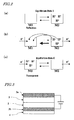
(Embodiment 1)
Firstly, a first embodiment of the dimming device
according to the present invention will be described with
reference to FIG. 3.
The dimming device of the present embodiment has a
layered structure including a dimming layer 1 and a
conversion layer 2, such that the light reflectance (optical
characteristics) of the dimming layer 1 changes in response
to electrical stimulations. This dimming device comprises a
pair of electrodes 3a, 3b sandwiching the dimming layer 1 and
the conversion layer 2, and a substrate 4 supporting the
layered structure. An appropriate voltage is to be
externally applied to the pair of electrodes 3a, 3b.
However, the electrode 3a and the electrode 3b may simply be
short-circuited as necessary.
Note that the layering order of the conversion layer 2
and dimming layer 1 with respect to the substrate 4 is not
limited to that which is shown. The conversion layer 2 may
be disposed so as to be closer to the substrate 4, with the
dimming layer 1 being formed thereabove.
The dimming layer 1 in the present embodiment contains a
dimming material (e.g., yttrium) whose optical
characteristics change in accordance with the hydrogen
concentration. The whole or part of the dimming layer 1 may
be composed of a single layer or multiple layers of dimming
material. Alternatively, particles of dimming material may
be present, in a dispersed or linked state, within a film
which is composed of another material.
The conversion layer 2 contains a conversion material
which is capable of containing hydrogen. This conversion
material performs exchanges of electrons with the electrode
3a, thus effecting release/absorption of hydrogen ions (H+).
In the illustrated example, a positive potential is
applied to the electrode 3a and a negative potential is
applied to the electrode 3b, whereby hydrogen ions are
released from the dimming material in the conversion layer 2
containing a sufficient amount of hydrogen in advance. The
released hydrogen ions move within an electric field which is
generated in the layered structure, and reach the dimming
layer 1, thus leaving the dimming material doped therewith.
Such a mechanism of hydrogen release and movement is as
described above. The dimming material in the dimming layer 1
bonds to hydrogen, thus forming a hydrogen metal compound.
As a result, the dimming material, which was initially in a
metallic state, changes to a semiconductor or insulator that
transmits visible light.
The dimming layer 1 may be produced by a vapor
deposition technique, a sputtering technique, or the like.
In the case where the dimming layer 1 is to function as a
mirror exhibiting a metallic luster, the dimming layer 1 is
preferably formed from a film which has as good a planarity
as possible.
The conversion material contained in the conversion
layer 2 is able to store and retain atoms or ions of hydrogen
in its stationary state, and changes its hydrogen storage
amount (retained amount) in accordance with external
stimulations. As this material capable of storing hydrogen,
alloys such as LaNi5, MnNi5, CaNi5 · TiMn1.5, ZrMn1.5, ZrMn2,
TiNi, TiFe, and Mg2Ni can be used. Moreover, carbon
nanotubes (CNT) may also be used.
The conversion layer 2 may contain an electrically
conductive material in addition to the hydrogen storage
material. If an electrically conductive material is
contained in the conversion layer 2, it is possible to
rapidly perform exchanges of hydrogen ions with the dimming
layer 1. As an electrically conductive material, a material
capable of ion transmission, such as a liquid or solid
electrolyte, or a conductive polymer or a charge transfer
complex which transmits charge (electrons or holes) can be
used. Moreover, in addition to the aforementioned hydrogen
storage material or electrically conductive material, a
bonding material such as a binder resin may be added to the
conversion layer 2 as necessary. Note that, in order to
surely restrain the charge which has been injected from one
electrode from immediately moving to the other electrode, a
separator layer may be inserted between the dimming layer and
the conversion layer. As the material of the separator
layer, it is desirable to choose a material which permits ion
movement but is unlikely to permit charge movement. For
example, an ion exchanger, a porous insulator, an ion
conductive polymer material or the like can be used. By
disposing a separate layer composed of such a material, the
charge which has been injected from an electrode is surely
prevented from penetrating to the other electrode, whereby
the charge movement efficiency between the dimming layer and
the conversion layer can be enhanced.
In the case where the conversion layer 2 is composed of
a mixture of a plurality of materials, a solution obtained by
dissolving such materials in a solvent may be prepared and
applied by a spin coating technique or a printing technique,
whereby the conversion layer 2 can be easily formed. Such
formation of the conversion layer 2 may be performed by an
ink jet technique or any other thin film deposition
technique.
As described above, according to the present embodiment,
exchanges of charges and ions occur inside the conversion
layer 2 responsive to application of a voltage to the
electrodes 3a, 3b. As a result, owing to the aforementioned
mechanism, hydrogen movement can be induced between the
conversion layer 2 and the dimming layer 1. Therefore, for
example, by using a dimming layer 1 which is undoped with
hydrogen in an initial state and a conversion layer 2 having
hydrogen stored in advance, if a voltage as shown in FIG.
1(a) is applied, hydrogen ions move from the positive side to
the negative side, thus making the dimming layer 1 doped
therewith. In other words, a hydrogen release reaction
progresses at the positive side, whereas a combination
reaction between hydrogen and a metal progresses at the
negative side, whereby a hydrogen metal compound is formed.
On the other hand, if a voltage in the opposite direction is
applied, a hydrogen movement in the opposite direction
occurs. Therefore, by reversing the polarity of the applied
voltage, the optical state of the dimming layer 1 can be
reversibly switched between metallic luster and transparent.
When only contemplating a movement of the hydrogen
stored in the conversion layer 2, the electrode 3a and the
electrode 3b might be short-circuited outside of the layered
structure. Such short-circuiting would be a similar
phenomenon to a discharging of a secondary battery, and
enable restoration of the internal state of the layered
structure to the initial state.
Since the conversion layer 2 and the dimming layer 1
have the ability to retain hydrogen, when voltage application
is not performed (when the external circuit is open), no
hydrogen movement occurs, so that the optical state of the
dimming layer 1 is retained (memory function of the dimming
layer). Therefore, by choosing a material having a good
hydrogen retaining ability, it becomes possible to retain a
dimmed state for a long period of time without consuming
power.
Contrary to the above example, a dimming layer 1 doped
with hydrogen in advance, and a conversion layer 2 in a state
not storing hydrogen may be used. In that case, hydrogen may
be moved from the dimming layer 1 to the conversion layer 2
by applying a positive potential to the dimming layer 1 and a
negative potential to the conversion layer 2, thus causing a
change in the optical state of the dimming material in the
dimming layer 1.
In the present embodiment, the light reflectance/light
transmittance of a dimming material can be controlled based
on a doping amount of hydrogen. Therefore, by controlling
the voltage to be applied to the electrode and application
time (e.g., a duty ratio), the light reflectance/light
transmittance of the dimming layer 1 can be controlled. By
utilizing the memory ability based on hydrogen retaining
ability, an appropriate light reflectance/light transmittance
can be easily retained.
In appropriately controlling such hydrogen
storage/release, it is necessary to pay attention to the
hydrogen equilibrium pressure-composition isotherm
(hereinafter referred to as a "PTC characteristic curve").
As shown in FIG. 4, the PTC characteristic curve represents a
relationship between the stored hydrogen amount and the
hydrogen equilibrium pressure. In the graph of FIG. 4, the
horizontal axis represents the hydrogen storage amount,
whereas the vertical axis represents the hydrogen equilibrium
pressure.
In a portion of the PTC characteristic curve that is
generally parallel to the horizontal axis (hereinafter
referred to as the "plateau region"), the stored hydrogen
amount is capable of changing under a constant equilibrium
pressure, and therefore hydrogen absorption/release can be
reversibly carried out in a state under a constant hydrogen
equilibrium pressure. For this reason, the dimming device of
the present embodiment performs switching operations in the
plateau region of the PTC characteristic curve.
It is desirable that the conversion layer 2 and the
dimming layer 1 exhibit substantially similar PTC
characteristics. More specifically, as shown in FIG. 4, it
is desirable that the ranges of "hydrogen storage amount" of
the plateau regions of the PTC characteristic curves of the
conversion layer 2 and the dimming layer 1 overlap each
other, and that the "hydrogen equilibrium pressure" levels
are substantially equal. By exhibiting similar hydrogen
equilibrium pressures, it becomes possible to smoothly
perform hydrogen exchanges between the dimming layer 1 and
the conversion layer 2. The reason is that, if the hydrogen
equilibrium pressure difference between the dimming layer 1
and the conversion layer 2 becomes large, it will be
impossible to perform hydrogen exchanges between the two
layers even if hydrogen absorption/release occurs in each
layer.
Moreover, it is more preferable that the hydrogen
storage amount range (span) of the plateau region of the PTC
characteristic curve of the conversion layer 2 is of a size
encompassing the hydrogen storage amount range (span) of the
plateau region of the PTC characteristic curve of the dimming
layer 1. The reason is that, in the dimming device of the
present embodiment, the light transmittance of the dimming
layer 1 is controlled by the hydrogen doping amount of the
dimming layer 1; therefore, if the extent of change in the
hydrogen storage amount of the conversion layer 2 were
smaller than the extent of change in the hydrogen doping
amount that is necessary for causing a state change of the
dimming layer 1, the optical state of the dimming layer 1
would not be sufficiently changed.
FIG. 3 is referred to again. In the case where the
conversion layer 2 is transparent, the dimming device shown
in FIG. 3 is capable of switching between a metallic
reflection state and a transparent state. In order to
establish a high transparency state, not only the substrate 4
and the electrodes 3a, 3b but also the conversion layer 2
must be formed from a material which has a high transmittance
(no absorption) in the entire visible light region. However,
a conversion material such as a hydrogen storage material is
often a metal or a colored material, and it is difficult to
form a conversion layer 2 having a high transparence from a
layer of such a conversion material. Therefore, it is
preferable to form the conversion layer 2 by mixing
microparticles of a conversion material with a transparent
material. Specifically, nanoparticles having a grain size
equal to or less than the light wavelength are formed from a
conversion material, and these nanoparticles may be bonded
with a binder resin which has a good transparence. A
conversion layer 2 thus produced is not only able to exhibit
both transparence and hydrogen storing ability, but an
increase in the hydrogen absorption/release efficiency can
also be expected since the conversion material has an
increased surface area because of being made into
nanoparticles. An increase in the hydrogen
absorption/release efficiency of the conversion material is
preferable because the response speed of the dimming
operation would be improved. As a conversion material in an
ultrafine particle state, a carbon type material (e.g., CNT
and fullerene), a potassium-graphite interlayer compound or
the like can also be used.
If a glass plate is used as the substrate 4, such a
dimming device functions as dimming glass. Dimming glass is
used as a windowpane for a building or an automobile, and by
increasing the light reflection amount when there is strong
external light as in the summertime or daytime, can restrain
strong external light from entering, thus creating a
comfortable space. It can also be used as an interior
article which doubles as transparent glass and a mirror.
(Embodiment 2)
Hereinafter, with reference to FIGS. 5(a) and (b), a
second embodiment of the dimming device according to the
present invention will be described. In the present
embodiment, switching between a metallic reflection state and
an absorbing (black) state can be performed, instead of
switching between a metallic reflection state and a
transparent state.
FIG. 5(a) and FIG. 5(b) show dimming devices of
constitutions featuring a conversion layer 2 and a dimming
layer 1 in opposite layering orders to each other. Light
enters from the rear face side of the substrate 4 in the
constitution of FIG. 5(a), whereas light enters from the
upper face side of the substrate 4 in the constitution of
FIG. 5(b). Both dimming devices comprise a conversion layer
2 which absorbs visible light. Such a conversion layer 2 can
be formed from a black CNT, for example. Note that, in the
case where the conversion layer 2 is colored, or even in the
case where the conversion layer 2 is transparent, if a
pigment or a colored resin is mixed therein, switching
between a metallic reflection state and a colored state is
possible.
In the dimming device shown in FIG. 5(a), it is
preferable that the substrate 4 and an electrode 3b in the
underlying layer are formed from a transparent material. The
substrate 4 may be formed from a material such as glass or
plastic, as long as it is transparent. Preferably, the
electrode 3b in the underlying layer is formed from a
transparent conductive material such as ITO. The preferable
electrode thickness in this case is prescribed to be 150 nm,
for example.
The dimming layer 1 is composed of a yttrium film having
a thickness of about 50 nm, for example. As the conversion
layer 2, for example, it is possible to use a blend of:
ultrafine particles (dispersion center radius: 10 nm) of an
Ni alloy, which is an AB5 type Mm hydrogen storage alloy; a
conductive polymer material P1 (a material capable of
transporting both charges, i.e., electrons and holes); and,
as a binder resin, an acrylic resin having about the same
refractive index as that of glass.
Since the blended resin can be made into a solution, a
film can be formed by spin coating. The thickness can be
about 500 nm. As the hydrogen storage alloy to be used for
the conversion layer 2, that which has hydrogen stored in
advance can be used. As the dimming material, La, MgNi, or
the like can be used other than yttrium.
In order to realize exchanges of charges and ions
between the dimming layer 1 and the conversion layer 2, it is
preferable to dispose a film of conductive polymer P1 between
the dimming layer 1 and the conversion layer 2. In addition
to a polymer film having a charge moving ability, a layer
formed by using an electrolyte material may be disposed.
Alternatively, a layer containing a polymer material having a
charge moving ability and an electrolyte material may be
disposed. By disposing such a film, movement of hydrogen
ions becomes likely to occur via the electrolyte, and
therefore it is possible to improve the characteristics.
A conversion layer 2 having light absorbing ability can
also be formed from what is obtained (blended resin) by
blending a potassium-graphite interlayer compound functioning
as a hydrogen storage material and a conductive polymer
material P1 (a material capable of transporting both charges,
i.e., electrons and holes) with an acrylic resin functioning
as a binder resin. Since the blended resin can be made into
a solution, the conversion layer 2 can be formed by spin
coating. The thickness of the conversion layer 2 may be
prescribed to about 500 nm, for example.
For the dimming device shown in FIG. 5(a), when a
voltage is applied to the electrodes 3a, 3b in such a manner
that the conversion layer 2 is the positive side and the
dimming layer 1 is the negative side, the light incident face
of the dimming device, which exhibited metallic reflection in
an initial state, gradually changes to a black state. This
is because, as the dimming layer 1 becomes transparent, the
black conversion layer 2 becomes visually perceivable. This
state is retained even after power is terminated. On the
other hand, if the electrode 3a and the electrode 3b are
short-circuited, or if a voltage with an inverted polarity is
applied to the electrodes 3a, 3b, the light incident-side
face of the dimming device changes so as to exhibit metallic
luster.
Note that, in the dimming device of the constitution
shown in FIG. 5(b), light enters from above the figure. In
this case, the electrode 3a in the upper layer of the dimming
layer 1 must be transparent, but the substrate 4 and the
underlying electrode 3 do not need to be transparent.
(Embodiment 3)
Next, with reference to FIG. 6(a), a third embodiment of
the dimming device according to the present invention will be
described.
The dimming device of the present embodiment comprises a
conversion layer 2 which is transparent with respect to
visible light, but further comprises a member which functions
as a light absorbing layer (light absorbing plate) 5, and
therefore is capable of switching between a metallic
reflection state and a black (light absorbing) state. The
light absorbing plate 5 may be a plate (black) that absorbs
light in the entire visible light region, or a plate (any
other color) that absorbs light in a part of the visible
light region.
The light absorber 5 is disposed on the opposite side
from the light incident side, with respect to the dimming
layer 1. In the present embodiment, as shown in FIG. 6(a),
the transparent conversion layer 2 is disposed above the
dimming layer 1. However, the upper/lower relationship of
the conversion layer 2 and the dimming layer 1 may be
reversed.
Instead of disposing the light absorbing plate 5 on the
rear face of the substrate, a layer having a light absorbing
ability may be disposed on the light incident-side face on
the substrate 4 or inside the layered structure. In the case
where such a light absorbing layer does not have
conductivity, it cannot be disposed between the dimming layer
1 and the electrode 3b, and therefore may be disposed between
the substrate 4 and the electrode 3b. On the other hand, in
the case where the light absorbing layer has conductivity,
the light absorbing layer can be employed in an integral
manner with the electrode 3b, or so as to replace the
electrode 3b.
Note that, by employing a light absorbing layer
exhibiting the same color and pattern as the color and
pattern of the wall material, it would become possible to
realize a dimming mirror which usually functions as part of
the wall but can exhibit a mirror function when necessary.
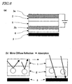
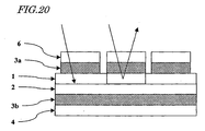
(Embodiment 4)
Next, with reference to FIG. 7 and FIG. 8, a fourth
embodiment of the dimming device according to the present
invention will be described. The dimming device of the
present embodiment is capable of switching between a metal
diffuse reflection (white) state and a light absorbing state.
As shown in FIG. 8, the dimming device of the present
embodiment has a structure in which an electrode 3a, a
conversion layer 2, a dimming layer 1, and an electrode 3b
are layered in this order on a substrate 4 having bumps and
dents. In order to effect diffuse-reflection, minute bumps
and/or dents are present on the surface of the dimming layer
1.
Next, with reference to FIG. 7, the operation of the
dimming device of FIG. 8 will be described.
In FIG. 7, the electrodes 3a, 3b are omitted from
illustration for simplicity. Since minute bumps are present
on the surface of the dimming layer 1, light can be diffuse-reflected
when the dimming layer 1 is in a metallic
reflection state as shown in FIG. 7(a). On the other hand,
when the dimming layer 1 is in a transparent state as shown
in FIG. 7(b), the conversion layer 2 in the underlying layer
absorbs light.
In the example shown in FIG. 7, the surface of the
substrate has minute bumps, and therefore the conversion
layer 2 and the dimming layer 1 are of such an overall
planarity that the bumps and dents of the substrate are
reflected in their shapes. In other words, not only the
upper face (the face on the light reflecting side) of the
dimming layer 1, but also the bottom face has a shape
reflecting the underlying bumps and dents. However, it is
not necessary for the underlying conversion layer 2 to have a
bump/dent structure. Therefore, minute dents and/or bumps
may be formed only on the upper face of the dimming layer 1,
while the substrate surface and the conversion layer 2 may be
formed flat.
Thus, in accordance with the dimming device of the
present embodiment, the reflected light is scattered and
perceived as white. Therefore, while the dimming layer 1 is
in a metallic reflection state, the surface of the dimming
layer 1 appears white. On the other hand, while the dimming
layer 1 is in a transparent state, the conversion layer 2
absorbs light, thus appearing black or some other color.
The dimming device of the present embodiment may have a
similar constitution to that of any other embodiment, except
that the substrate 4 having bumps and dents formed on its
surface is used. For example, as the conversion layer 2,
what is obtained by blending a potassium-graphite interlayer
compound which is a hydrogen storage material, a conductive
polymer material P1 (a material capable of transporting both
charges, i.e., electrons and holes), and an acrylic resin
serving as a binder resin can be suitably used.
(Embodiment 5)
With reference to FIG. 9, a fifth embodiment of the
dimming device according to the present invention will be
described.
In dimming device of the present embodiment, as shown in
FIG. 9, the dimming layer 1 itself doubles as one of the
electrodes. Since the dimming layer 1 is fundamentally a
metal thin film, the dimming layer 1 can function as an
electrode. Since the dimming layer 1 doubles as an
electrode, a step of forming an electrode is omitted, whereby
the number of production steps for the dimming device can be
reduced.
Note that, although the dimming device shown in FIG. 9
is a transparent-metal reflection type dimming device, the
dimming layer 1 can double as an electrode in a dimming
device of any other type described above.
(Embodiment 6)
With reference to FIG. 10, a sixth embodiment of the
dimming device according to the present invention will be
described.
The present embodiment has a constitution in which a
conversion layer is separated into a plurality of layers,
i.e., a first conversion layer 2a, and a second conversion
layer 2b. In the dimming device according to the present
invention, the dimming layer 1 is doped with a specific
element such as hydrogen, whereby the state of the dimming
layer 1 is changed. Therefore, by adopting the constitution
in which two conversion layers 2a, 2b sandwich the dimming
layer 1, efficient doping becomes possible, whereby the speed
of the state change necessary for dimming is improved. Since
the dimming layer 1 can function as an electrode, the dimming
layer 1 is used as an electrode in the example of FIG. 10.
In the example of FIG. 10, the portion which performs
hydrogen absorption/release has a three-layer structure
including the first conversion layer 2a, the dimming layer 1,
and the second conversion layer 2b, but may have even more
layers. Even if sufficient dimming cannot be attained in the
case where the dimming layer 1 is of a single layer, it would
become possible to attain a sufficient dimming by increasing
the number of layers in the dimming layer 1.
(Embodiment 7)
With reference to FIG. 11, a seventh embodiment of the
dimming device according to the present invention will be
described.
In the present embodiment, the conversion layer 2 has a
multi-layer structure in order to separate the functions of
the conversion layer 2. As described above, the functions of
the conversion layer 2 are to store hydrogen, and to
release/re-store hydrogen in accordance with charge
injection/release. Rather than realizing these functions
with a single material, it would be easier to select a
different material for each function, and stack layers that
are composed of the respective materials. In other words, by
separating the conversion layer into a first conversion layer
2a composed of a charge transport material or an electrolyte
material for performing exchanges of charges or ions and a
second conversion layer 2b formed from a material having a
hydrogen storing function, efficient hydrogen movement can be
realized.
In the present embodiment, a charge ·ion exchange layer
formed by mixing a conductive polymer material P1 (a material
capable of transporting both charges, i.e., electrons and
holes) and an acrylic resin having about the same refractive
index as that of glass is used as the first conversion layer
2a. Moreover, a blended resin obtained by mixing ultrafine
particles (dispersion center radius: 10 nm) of an Ni alloy,
which is an AB5 type Mm hydrogen storage alloy, and an
acrylic resin having about the same refractive index as that
of glass is used so as to function as the second conversion
layer 2b.
(Embodiment 8)
Hereinafter, with reference to FIG. 12, an eighth
embodiment of the dimming device according to the present
invention will be described.
The present embodiment differs from each of the above-described
embodiments in that no electrode structure is
comprised, as shown in FIG. 12. In the present embodiment, a
material having photocharge generating characteristics is
added to the conversion layer 2. Herein, a material having
photocharge generating characteristics means a material
system which releases electrons or holes upon light
irradiation. Specifically, it includes a fluorescent dye,
SiO2 microparticles, or organic molecules such as carbazole,
or a polymer material obtained by polymerizing the same.
Such materials release holes or electrons responsive to light
irradiation, in accordance with their respective absorption
wavelengths. Such charge causes the hydrogen contained in
the hydrogen storage material to be isolated, transmitted
within the conversion layer so as to be brought to the metal
film of the dimming layer, thus hydrogenating the metal film.
Usually, a material showing absorption in the visible light
region is preferably used because dimming is to be performed
in the visible light region. However, in the case where it
is desirable to control the dimming amount based on the
intensity of ultraviolet rays or heat rays (infrared rays), a
material system showing absorption in such regions may be
used.
This dimming device, whose conversion layer has
photocharge generating characteristics, is characterized by
its ability to perform dimming without particularly using an
external control system such as an electric field. Since
charge release takes place during light irradiation, it is
possible to control the dimming amount.
As for the controlling of the initial state, hydrogen
may be stored in the hydrogen storage material in the
conversion layer, and the dimming layer may be kept in a non-doped
state, whereby a metallic reflection state is obtained
as an initial state. If the dimming layer is doped with
hydrogen in advance, the dimming layer takes a transparent
state, so that the initial state is determined by the
coloration of the conversion layer.
Moreover, in the dimming amount control based on light
irradiation, the dimming amount will vary with light amount
accumulation. Therefore, there may be cases where even weak
light may cause a change in the dimming amount if irradiation
continues for a long time. This may be a problem if it is
desirable to control the dimming amount based only on the
intensity of light irradiation. In such cases, the hydrogen
storing abilities of the conversion layer and the dimming
layer, i.e., reaction speed with hydrogen, are to be
adjusted. In the case where equilibrium is strongly shifted
toward the dimming layer, even if incident light causes
hydrogen to be transmitted to the conversion layer and leaves
the conversion layer to be doped with hydrogen, most of the
hydrogen is returned to the dimming layer. Furthermore, by
controlling the irradiation amount that would exhibit
conversion, the transparent state (hydrogen doped state) of
the conversion layer can maintain the transparent state of
the dimming layer while a certain intensity of light
irradiation is being provided. In the case where the light
irradiation is weak, or there is no more light irradiation,
the equilibrium state will shift toward the conversion layer,
so that the dimming layer will return to the initial state.
In the case where the metallic reflection-transparent states
of the dimming layer are repeatedly used with light
irradiation, the direction of equilibrium state with respect
to the dimming layer and the conversion layer may also be
controlled.
In the present embodiment, as the dimming material in
the dimming layer 1, a material whose PTC characteristic
curve shows, in its flat region, an equilibrium pressure
which is greater than that of the conversion material in the
conversion layer 2 is chosen.
In the conversion layer 2, an Ru complex dye is
additionally added. This dye absorbs light in the entire
visible light region, and has characteristics such that it
releases electrons upon light absorption. Moreover, the
conversion layer 2 has hydrogen stored in advance.
If the dimming device of the present embodiment is
irradiated with light, the degree of metallic reflection
lowers when the light irradiation amount has reached a
sufficient level, so that the dimming device begins to appear
black. This happens because the electrons generated due to
light irradiation cause a reduction reaction in the hydrogen
storage material in the conversion layer 2, and the resultant
hydrogen exceeds the hydrogen equilibrium pressure in the
dimming layer 1. The hydrogen which has moved to the dimming
layer 1 forms a hydrogenated compound therein, and makes the
dimming layer 1 transparent. As a result, the color (black)
of the conversion layer 2 is visually perceived through the
dimming layer 1.
When light irradiation is stopped, the generation/supply
of electrons stops, so that the state change of the dimming
layer 1 also stops. Since a difference in hydrogen
equilibrium pressure has occurred, the equilibrium state
shifts toward the conversion layer, and most of the hydrogen
which has moved to the dimming layer can again move to the
conversion layer.
Thus, according to the present embodiment, the dimming
amount can naturally be adjusted based on light irradiation.
In the exemplary constitution above, the amount of reflection
by the dimming layer 1 becomes smaller as the light
irradiation intensity increases. However, by using a
transparent material for the conversion layer and doping the
dimming layer with hydrogen in advance, it becomes possible
to provide a windowpane which can control transmission and
reflection in accordance with light intensity. In this case,
the dye which is included in the conversion layer becomes
colored. Therefore, a completely transparent state would be
difficult to obtain, but a device embodying color glass and
reflection can be easily produced.
Instead of switching the state change of the dimming
layer based on external light irradiation, it would be
possible to control the hydrogen equilibrium state in
accordance with intensity of irradiation light or a
cumulative value of irradiation amounts to realize dimming.
In the case where dimming is performed based only on light
irradiation, it would be impossible to realize a dimming
which is in accordance with the needs of the user. There may
also be a problem in that hydrogen cannot be completely moved
during the use of the dimming device, thus causing a shift in
the initial state. In order to avoid such problems, it would
be preferable to additionally provide electrodes. By
adjusting the hydrogen doped amount with the additionally-provided
electrodes, in conjunction with the dimming based on
usual light irradiation, it will become possible to freely
change the dimming amount. Moreover, initialization to a
hydrogen equilibrium state can be performed by voltage
application using electrodes, so that a dimming control which
permits good reproducibility can be realized.
(Embodiment 9)
The dimming device of the present embodiment has a
similar constitution to that of the dimming device of
Embodiment 1 which has been described with reference to FIG.
3, except that the dimming layer 1 contains dimming
particles. The dimming device of the present embodiment
performs switching between a metal diffuse reflection state
and a transparent state by utilizing the dimming principle
illustrated in FIG. 1(b).
In the dimming layer 1 of the present embodiment,
microparticles (e.g., yttrium or lanthanum, hereinafter
referred to as "dimming microparticles") which have been
formed by using a dimming material whose optical
characteristics change in accordance with hydrogen
concentration are dispersed in a binder resin.
The average grain size of the dimming microparticles
contained in the dimming layer 1 is 1 µm, for example. The
dimming microparticles are typically dispersed in a binder
resin. As a binder resin, an acrylic resin having about the
same refractive index as that of glass is used. Moreover,
the dimming layer 1 further contains an electrically
conductive material for performing exchanges of hydrogen ions
and charge between the dimming microparticles and the
conversion layer 2. As the electrically conductive material,
a material capable of ion transmission, such as a liquid or
solid electrolyte, or a conductive polymer (e.g., P2) or a
charge transfer complex which transmits charge (electrons or
holes) can be used.
The dimming layer 1 can be formed by preparing an
application solution by dispersing the aforementioned dimming
microparticles in a solution of binder resin, and further
dissolving an electrically conductive material therein, and
thereafter applying the application solution onto the
electrode 3b by a spin coating technique, for example. The
thickness of the dimming layer 1 is about 3 µm, for example.
The formation of the dimming layer 1 may be performed by an
ink jet technique or any other thin film deposition
technique. The light incident-side face of the dimming layer
1 may be flat, or have bumps and dents. A dimming layer 1
having bumps and dents can be formed by using a substrate 4
or electrode 3b having bumps and dents and applying the
aforementioned application solution onto the under layer
having bumps and dents, for example.
The preferable thickness of the dimming layer 1 is no
less than 1.5 µm and no more than 50 µm. If it is equal to
or less than 1.5 µm, it may be impossible to obtain a dimming
layer 1 having a high reflectance, or the grain size of the
dimming microparticles used in the dimming layer 1 may be
limited. On the other hand, if it is equal to or greater
than 50 µm, the conductivity of the dimming layer 1 may be
lowered.
The conversion layer 2 has a similar constitution to
that of the conversion layer 2 in Embodiment 1, and may be
formed by using a similar material.
In the present embodiment, similarly to Embodiment 1,
the dimming device can be operated by applying a voltage to
the electrodes 3a, 3b so as to induce a hydrogen movement
between the conversion layer 2 and the dimming
microparticles.
Preferably, the hydrogen storage/release is
appropriately controlled by using a PTC characteristic curve
shown in FIG. 4, as described in Embodiment 1. In other
words, it is desirable that the conversion layer 2 and the
dimming layer 1 exhibit substantially similar PTC
characteristics. More specifically, as shown in FIG. 4, it
is desirable that the ranges of "hydrogen storage amount" of
the plateau regions of the PTC characteristic curves of the
conversion layer 2 and the dimming layer 1 overlap each
other, and that the "hydrogen equilibrium pressure" levels
are substantially equal. Moreover, it is more preferable
that the hydrogen storage amount range (span) of the plateau
region of the PTC characteristic curve of the conversion
layer 2 is of a size encompassing the hydrogen storage amount
range (span) of the plateau region of the PTC characteristic
curve of the dimming layer 1.
(Embodiment 10)
The dimming device of the present embodiment has a
similar constitution to that of the dimming device of
Embodiment 2 described with reference to FIGS. 5(a) to (c),
except that the dimming layer 1 contains dimming particles.
Utilizing the dimming principle illustrated in FIG. 1(b), the
dimming device of the present embodiment is capable of
switching between a metal diffuse reflection (white) state
and an absorbing (black or colored) state.
The dimming layer 1 is similar to the dimming layer 1
used in Embodiment 9, for example. A conversion layer 2
having a light absorbing ability can also be formed from what
is obtained (blended resin) by blending a potassium-graphite
interlayer compound functioning as a hydrogen storage
material and a conductive polymer material P1 (a material
capable of transporting both charges, i.e., electrons and
holes) with an acrylic resin functioning as a binder resin.
Since the blended resin can be made into a solution, the
conversion layer 2 can be formed by spin coating. The
thickness of the conversion layer 2 may be prescribed to
about 500 nm, for example.
In order to realize exchanges of charges and ions
between the dimming layer 1 and the conversion layer 2, it is
preferable to dispose a film of conductive polymer P1 between
the dimming layer 1 and the conversion layer 2. Instead of
disposing a polymer film having a charge moving ability, an
electrolyte film may be disposed. By disposing an
electrolyte film, movement of hydrogen ions becomes likely to
occur via the electrolyte, and therefore it is possible to
improve the characteristics.
Note that, in the dimming device of the constitution
shown in FIG. 5(b), light enters from above the figure. In
this case, the electrode 3a in the upper layer of the dimming
layer 1 must be transparent, but the substrate 4 and the
underlying electrode 3 do not need to be transparent.
For the dimming device shown in FIG. 5(a) and FIG. 5(b),
when a voltage is applied to the electrodes 3a, 3b in such a
manner that the conversion layer 2 is the positive side and
the dimming layer 1 is the negative side, the dimming layer
1, which exhibited metal diffuse reflection in an initial
state, gradually changes to a black state, as shown in FIG.
5(c). This is because, as the dimming microparticles
contained in the dimming layer 1 become transparent, the
black conversion layer 2 becomes visually perceivable. This
state is retained even after power is terminated. On the
other hand, if the electrode 3a and the electrode 3b are
short-circuited, or if a voltage with an inverted polarity is
applied to the electrodes 3a, 3b, the dimming layer 1 changes
so as to exhibit metal diffuse luster.
(Embodiment 11)
Next, with reference to FIGS. 6(a) and (b), an eleventh
embodiment of the dimming device according to the present
invention will be described. The dimming device of the
present embodiment has a similar constitution to that of
Embodiment 3 described with reference to FIG. 6(a), except
that the dimming layer 1 contains dimming microparticles. In
other words, by utilizing the dimming principle shown in FIG.
1(b), the dimming device of the present embodiment is capable
of switching between a metal diffuse reflection state and a
black (light absorbing) state.
The dimming layer 1 and the conversion layer 2 in the
present embodiment may be identical to the dimming layer 1
and conversion layer 2 in Embodiment 9. Moreover, the light
absorbing plate 5 may be identical to the light absorbing
plate 5 in Embodiment 3.
For the dimming device shown in FIG. 6(a), when a
voltage is applied to the electrodes 3a, 3b in such a manner
that the conversion layer 2 is the positive side and the
dimming layer 1 is the negative side, the dimming layer 1,
which exhibited metal diffuse reflection in an initial state,
gradually changes to a black state, as shown in FIG. 6(b).
This is because, as the dimming microparticles contained in
the dimming layer 1 become transparent, the black conversion
layer 2 becomes visually perceivable. This state is retained
even after power is terminated. On the other hand, if the
electrode 3a and the electrode 3b are short-circuited, or if
a voltage with an inverted polarity is applied to the
electrodes 3a, 3b, the dimming layer 1 changes so as to
exhibit metal diffuse luster.
(Embodiment 12)
Next, a twelfth embodiment of the dimming device
according to the present invention will be described. The
dimming device of the present embodiment has a similar
constitution to that of Embodiment 9 described with reference
to FIG. 3. There is a difference in that the dimming layer 1
and the conversion layer 2 of the present embodiment utilize
the dimming principle shown in FIG. 1(c). Therefore, without
using a conversion layer 2 exhibiting light absorbing ability
as in Embodiment 10, or without providing a light absorbing
plate 5 as in Embodiment 11, it is possible to switching
between a perform metal diffuse reflection (white) state and
a light absorbing (black or colored) state.
As shown in FIG. 3, the dimming device of the present
embodiment has a structure in which an electrode 3a, a
dimming layer 1, a conversion layer 2, and an electrode 3b
are layered in this order on a substrate 4. In this dimming
device, light enters at the upper face of the substrate 4.
Note that the layering order of the dimming layer 1 and the
conversion layer 2 may be reversed, in which case light would
enter at the rear face of the substrate 4.
The dimming layer 1 contains dimming microparticles
(e.g., yttrium microparticles) similar to those used in
Embodiment 9. The dimming microparticles are adsorbed to
carbon-type black particles, for example.
Such a dimming layer 1 can be formed as follows, for
example. In a solution of binder resin, black particles
having a grain size of 5µm and dimming microparticles having
a smaller grain size (e.g., 1 µm) are mixed, and dimming
microparticles are allowed to adsorb so as to cover the
surface of the black particles. After a conductive polymer
material P2 is further blended to the resultant solution, the
resultant blend solution is applied onto the electrode 3b by
a spin coating technique. The thickness of the dimming layer
1 is 10 µm, for example. Since the black particles are
dispersed, the thickness of the dimming layer 1 is greater
than the thickness of the dimming layer 1 in any other
embodiment. However, since the carbon-type black
microparticles and the dimming microparticles both exhibit a
high conductivity, the entire dimming layer 1 has a
sufficient conductivity.
For the dimming device of the present embodiment, when a
voltage is applied to the electrodes 3a, 3b in such a manner
that the conversion layer 2 is the positive side and the
dimming layer 1 is the negative side, the light incident face
of the dimming device, which exhibited metal diffuse
reflection in an initial state, gradually changes to a black
state. This is because, as the dimming microparticles
adsorbed to the black particles become transparent, the black
particles become visually perceivable. This state is
retained even after power is terminated. On the other hand,
if the electrode 3a and the electrode 3b are short-circuited,
or if a voltage with an inverted polarity is applied to the
electrodes 3a, 3b, the light incident-side face of the
dimming device changes so as to exhibit metal diffuse luster.
Thus, in accordance with the dimming device of the
present embodiment, when the dimming microparticles contained
in the dimming layer 1 are in a metallic reflection state,
reflected light is scattered so as to be perceived as white,
whereby the surface of the dimming layer 1 appears white. On
the other hand, when the dimming microparticles are in a
transparent state, light is absorbed by the colored particles
such as black particles, so that the surface of the dimming
layer 1 appears black or in any other color. In other words,
the dimming layer 1 itself transitions between a metal
diffuse state and a light absorbing (colored) state.
Therefore, in the present embodiment, without separately
providing a layer having a light absorbing ability, e.g., an
absorption plate, a dimming device which is capable of
switching between a metal diffuse state a light absorbing
(colored) state can be provided.
The dimming device of the present embodiment can have a
similar constitution to that of Embodiment 9, except that a
dimming layer 1 containing colored particles as described
above is used. However, the layers which are located closer
to the light incident side than is the dimming layer 1 (i.e.,
the conversion layer 2 and the electrode 3a in the
constitution of FIG. 3) are transparent. On the other hand,
the layers which are not located closer to the light incident
side than is the dimming layer 1 (i.e., the electrode 3b and
the substrate 4 in the constitution of FIG. 3) do not need to
be transparent.
(Embodiment 13)
With reference to FIGS. 13(a) and (b), a thirteenth
embodiment of the dimming device according to the present
invention will be described.
The dimming device of FIG. 13(a) has a constitution in
which a conversion layer is separated into a plurality of
layers, i.e., a first conversion layer 2a and a second
conversion layer 2b. In the dimming device according to the
present invention, the dimming layer 1 is doped with a
specific element such as hydrogen, whereby the state of the
dimming layer 1 is changed. Therefore, by adopting the
constitution in which two conversion layers 2a, 2b sandwich
the dimming layer 1, efficient doping becomes possible,
whereby the speed of the state change necessary for dimming
is improved. Since the dimming layer 1 can function as an
electrode, the dimming layer 1 is used as an electrode in the
example of FIG. 13(a).
In the dimming device of FIG. 13(a), the portion which
performs hydrogen absorption/release has a three-layer
structure including the first conversion layer 2a, the
dimming layer 1, and the second conversion layer 2b, but may
have even more layers. Even if sufficient dimming cannot be
attained in the case where the dimming layer 1 is of a single
layer, it would become possible to attain a sufficient
dimming by increasing the number of layers in the dimming
layer 1.
In the case where the dimming layer 1 has such a low
conductivity that it cannot be used as an electrode, as shown
in FIG. 13(b), the dimming layer may be separated into two
layers, i.e., a first dimming layer 1a and a second dimming
layer 1b, and an electrode 3c may be inserted between these
dimming layers. In the dimming device of FIG. 13(b), too,
the dimming layer 1 may have even more layers.
The dimming device of either FIG. 13(a) or (b) can be
easily produced by sequentially stacking the respective
layers. Note that the dimming layer, the conversion layer,
the electrodes, and the substrate may have similar
constitutions to those in Embodiments 9 to 12 except that the
number of stacked layers may be different.
(Embodiment 14)
The dimming device of the present embodiment has a
similar constitution to that of Embodiment 6 described with
reference to FIG. 11. However, as the dimming layer 1, a
dimming layer 1 having a structure as shown in FIG. 1(b) or
(c) is used.
In the present embodiment, the conversion layer 2 is
separated into a first conversion layer 2a and a second
conversion layer 2b having different functions. The first
and second conversion layers 2a, 2b may be formed from
similar materials to those of the first and second conversion
layers 2a, 2b in Embodiment 6.
Note that such separation of functions of the conversion
layers can also be applied to the dimming device of any of
Embodiments 9 to 13.
(Embodiment 15)
The dimming device of the present embodiment has a
similar constitution to that of Embodiment 8 described with
reference to FIG. 12. However, as the dimming layer 1, a
dimming layer 1 having a structure as shown in FIG. 1(b) or
(c) is used.
In the conversion layer 2 of the present embodiment, a
material having photocharge generating characteristics is
added. As a material having photocharge generating
characteristics, any material exemplified in Embodiment 8 can
be used. Moreover, the dimming device of the present
embodiment can be allowed to operate by the control method
described in Embodiment 8.
According to the present embodiment, the dimming amount
can naturally be adjusted based on light irradiation.
Therefore, there is an advantage in that electrodes 3a, 3b
(e.g., FIG. 5) for applying a voltage to the dimming layer 1
and the conversion layer 2 are not necessary.
(Embodiment 16)
Hereinafter, with reference to FIG. 14 and FIG. 15, a
sixteenth embodiment of the dimming device according to the
present invention will be described.
The present embodiment differs from the above-described
embodiments in that, as shown in FIG. 14, only the dimming
layer 1 is layered on the substrate 4, and no electrodes or
conversion layer is comprised. The substrate 4 only needs to
be a transparent substrate, and a substrate similar to that
used in any other embodiment can be used.
FIG. 15 shows a dimming layer 1 used in the dimming
device of the present embodiment. The dimming layer 1
includes dimming microparticles 11, a material 12 having
photocharge generating characteristics such as an Ru complex
dye, and a conversion material 13 such as a hydrogen storage
material. These are typically dispersed in a binder resin.
Moreover, the dimming layer 1 contains an electrically
conductive material for enabling hydrogen or electrons to
move within the dimming layer 1. In the present embodiment,
as a dimming material composing the dimming microparticles
11, a material whose PTC characteristic curve shows, in its
flat region, an equilibrium pressure which is greater than
that of the conversion material 13 is selected. As the
material 12 having photocharge generating characteristics, a
similar material to that which is exemplified in Embodiment 7
can be used. As the conversion material 13, the same
conversion material as that contained in the conversion layer
in any other embodiment can be used. Thus, the dimming layer
1 contains all constituents that are necessary for causing
optical modulation.
If the dimming device of the present embodiment is
irradiated with light, the degree of metal diffuse reflection
lowers when the light irradiation amount has reached a
sufficient level, so that the dimming device begins to appear
transparent. The reason is as follows. The electrons
generated due to light irradiation induce a reduction
reaction in the conversion material 13, and thus hydrogen is
produced. When the resultant hydrogen exceeds the hydrogen
equilibrium pressure in the conversion material 13, the
hydrogen moves to the dimming microparticles 11, thus forming
a hydrogenated compound with the dimming material of the
dimming microparticles. When a hydrogenated compound is
formed, the dimming microparticles 11 become transparent. As
a result, the entire dimming device becomes transparent.
When light irradiation is stopped, the generation/supply
of electrons stops, so that the state change of the dimming
layer 1 also stops. Since a difference in hydrogen
equilibrium pressure has occurred, the equilibrium state
shifts toward the conversion material 13, and most of the
hydrogen which has moved to the dimming microparticles 11 can
again move to the conversion material 13.
Thus, according to the present embodiment, the dimming
amount can naturally be adjusted based on light irradiation.
In the present embodiment, too, as in Embodiment 15, it
would also be possible to control the hydrogen equilibrium
state in accordance with intensity of irradiation light or a
cumulative value of irradiation amounts to realize dimming.
Moreover, by additionally disposing electrodes, it would
become possible to adjust the hydrogen doped amount.
(Embodiment 17)
Hereinafter, with reference to FIG. 14 and FIG. 16, a
seventeenth embodiment of the dimming device according to the
present invention will be described.
As shown in FIG. 14, in the dimming device of the
present embodiment, only the dimming layer 1 is layered on
the substrate 4, and no electrodes or conversion layer is
comprised. In the present embodiment, the substrate 4 only
needs to be able to support the dimming layer 1, and does not
need to be transparent.
FIG. 16 shows a dimming layer 1 used in the dimming
device of the present embodiment. In the dimming layer 1,
colored particles (e.g., black particles) 10 are dispersed in
a binder resin, with dimming microparticles 11 being adsorbed
to the colored particles 10. Other than that, a material 12
having photocharge generating characteristics such as an Ru
complex dye and a conversion material 13 such as a hydrogen
storage material are dispersed in the binder resin.
Furthermore, the dimming layer 1 contains an electrically
conductive material for enabling hydrogen or electrons to
move within the dimming layer 1. In the present embodiment,
as a dimming material composing the dimming microparticles
11, a material whose PTC characteristic curve shows, in its
flat region, an equilibrium pressure which is greater than
that of the conversion material 13 is selected. As the
material 12 having photocharge generating characteristics, a
similar material to that which is exemplified in Embodiment 7
can be used. As the conversion material 13, the same
conversion material as that contained in the conversion layer
in any other embodiment can be used. Thus, the dimming layer
1 contains all constituents that are necessary for causing
optical modulation.
In the present embodiment, as the colored particles 10,
black particles of a potassium-graphite interlayer compound
are used. Thus, it is preferable if the colored particles 10
are particles which can also function as a conversion
material because then it would be unnecessary to separately
add the conversion material 13 to the dimming layer 1.
Moreover, since the dimming microparticles 11 are adsorbed to
the colored particles 10, which are the conversion material,
the time required for hydrogen to move between the dimming
material and the conversion material is short. Therefore, as
compared to the case where hydrogen moves within the binder
resin, the optical characteristics of the dimming layer 1 can
be switched rapidly.
If the dimming device of the present embodiment is
irradiated with light, the degree of metal diffuse reflection
lowers when the light irradiation amount has reached a
sufficient level, so that the dimming device begins to assume
the color of the colored particles 10, e.g., black. This
happens because, the electrons generated due to light
irradiation induce a reduction reaction in the conversion
material (i.e., the conversion material 13, or the colored
particles 10 in the case where the colored particles 10 are
formed by using a conversion material), and the resultant
hydrogen exceeds the hydrogen equilibrium pressure in the
conversion material. The hydrogen moves from the conversion
material to the dimming microparticles 11 to form a
hydrogenated compound with the dimming material of the
dimming microparticles 11, thus making the dimming
microparticles 11 transparent. As a result, the color of the
colored particles 10 is visually perceived, whereby the
entire dimming device assumes the color of the colored
particles 10.
When light irradiation is stopped, the generation/supply
of electrons stops, so that the state change of the dimming
layer 1 also stops. Since a difference in hydrogen
equilibrium pressure has occurred, the equilibrium state
shifts toward the conversion material, and most of the
hydrogen which has moved to the dimming microparticles 11 can
again move to the conversion material.
Thus, according to the present embodiment, the dimming
amount can naturally be adjusted based on light irradiation.
In the present embodiment, too, as in Embodiment 15, it
would also be possible to control the hydrogen equilibrium
state in accordance with intensity of irradiation light or a
cumulative value of irradiation amounts to realize dimming.
Moreover, by additionally disposing electrodes, it would
become possible to adjust the hydrogen doped amount.
(Embodiment 18)
First, with reference to the figures, an eighteenth
embodiment of the present invention will be described. The
present embodiment is directed to a display device utilizing
the above-described dimming principle.
FIG. 17 shows a schematic cross-sectional view of one
pixel of the display device of the present embodiment. FIG.
18 shows a plan view of the display device of the present
embodiment. Although a reflection type full-color display
device will herein be illustrated for instance, the present
invention is not limited thereto. For example, it may be a
monochrome display device or a projection type display
device.
The display device of the present embodiment includes a
light absorbing layer 5, electrodes 3b, a conversion layer 2,
a dimming layer 1, electrodes 3a, and color filters 6 layered
in this order on a substrate 1. As shown in FIG. 18, the
electrodes 3b include a plurality of patterns extending in
parallel, whereas the electrodes 3a include a plurality of
patterns extending in a direction perpendicular to the
electrodes 3b. An appropriate voltage can be applied to each
pair of electrodes 3a, 3b. However, it would also be
possible to simply short-circuit the electrodes 3a and
electrodes 3b as necessary. The color filters 6 include a
plurality of patterns extending substantially in parallel to
the electrodes 3a. Among these patterns, typically three
patterns of R(red), G(green), and B(blue) are formed for each
pixel.
Note that the layering order of the conversion layer 2
and the dimming layer 1 with respect to the substrate 4 is
not limited to that which is illustrated in the figures, but
the conversion layer 2 may be disposed so as to be closer to
the substrate 4, with the dimming layer 1 being formed
thereupon. If the substrate 4 is a transparent substrate
such as a glass substrate, the light absorbing layer 5 may be
provided on the rear face of the substrate 4. In the case
where the light absorbing layer 5 has conductivity, the light
absorbing layer 5 may be provided anywhere between the
electrodes 3a and the electrodes 3b. Alternatively, a light
absorbing layer 5 having conductivity can be used in an
integral manner with the electrodes 3b, or so as to replace
the electrodes 3b.
The dimming layer 1 in the present embodiment contains a
dimming material (e.g., yttrium) whose optical
characteristics change in accordance with the hydrogen
concentration. In the present embodiment, the dimming layer
1 is a film (e.g., a yttrium film) formed by using a dimming
material as shown in FIG. 1(a). The dimming layer 1 may be a
single layer or have a multi-layer structure.
The conversion layer 2 contains a conversion material
which is capable of containing hydrogen. This conversion
material performs exchanges of electrons with the electrodes
3a, thus effecting release/absorption of hydrogen ions (H+).
In the illustrated example, a voltage can be applied to
the conversion layer 2 in any arbitrary pixel by means of the
matrix-shaped electrodes 3a and 3b. In a given pixel, by
applying a positive potential to the electrode 3a and a
negative potential to the electrode 3b, hydrogen ions are
released from the conversion material in the conversion layer
2 containing a sufficient amount of hydrogen in advance. The
released hydrogen ions move within an electric field which is
generated in the layered structure, and reach the dimming
layer 1, thus leaving the dimming material doped therewith.
Such a mechanism of hydrogen release and movement is as
described above. The dimming material in the dimming layer 1
bonds to hydrogen, thus forming a hydrogen metal compound.
As a result, the dimming material, which was initially in a
metallic state, changes to a semiconductor or insulator that
transmits visible light.
The aforementioned changes in the states of the dimming
layer 1 and the conversion layer 2 are shown in FIG. 19(a).
When the dimming material in the dimming layer 1 is in a
metallic state, light entering the display device is
reflected from the dimming layer 1, thus being transmitted
through the color filter 6. Therefore, the light which has
been transmitted through the color filter 6 is visually
perceived. When the dimming material becomes a semiconductor
or an insulator, the dimming layer 1 becomes transparent, and
therefore the light entering the display device is
transmitted through the dimming layer 1 and absorbed by the
light absorbing layer 5. As a result, black is visually
perceived.
Next, a method of producing the display device of the
present embodiment will be described.
First, the substrate 4 is prepared. The substrate 4
only needs to be able to support the layered structure formed
on the substrate 4, and a glass substrate, a plastic
substrate, or a metal substrate may be used. The substrate 4
does not need to be transparent.
The light absorbing layer 5 is formed on the substrate
1. The light absorbing layer 5 may be a layer (black) that
absorbs light in the entire visible light region, or a layer
(any other color) that absorbs light in a part of the visible
light region. The formation of the light absorbing layer 5
is performed by applying a black resin containing a carbon
black-type black material onto the substrate 1 by a spin
coating technique, for example.
Thereafter, electrodes are formed on the light absorbing
layer 5. For example, by using ITO (Indium Tin Oxide), a
film having a thickness of 150 nm is formed by a sputtering
technique. This film is patterned into a plurality of
patterns having a.width of 100µm (corresponding to the width
of the pixel). These patterns are substantially parallel to
one another, with an interspace of 10µm present between
adjoining patterns.
On the electrodes 3b, the transparent conversion layer 2
is formed. The conversion material contained in the
conversion layer 2 can store and retain atoms or ions of
hydrogen in its stationary state, and changes its hydrogen
storage amount (retained amount) in accordance with external
stimulations. As this material capable of storing hydrogen,
those materials exemplified in Embodiment 1 can be used.
The conversion layer 2 may contain an electrically
conductive material in addition to the hydrogen storage
material. As the electrically conductive material, those
materials exemplified in Embodiment 1 can be used. To the
conversion layer 2, a bonding material such as a binder resin
may be added as necessary, in addition to the aforementioned
hydrogen storage material and electrically conductive
material.
The charge which has been injected from the electrodes
3a, 3b undergoes charge exchanges in the dimming layer 1 and
the conversion layer 2. Since the charge which has been
injected from one of the electrodes may immediately move to
the other electrode, a layer to serve as a separator
(separate layer), e.g., an ion exchange film, may be disposed
between the dimming layer 1 and the conversion layer 2. It
is desirable that the separate layer is formed from a
material which permits ion movement but is unlikely to permit
charge movement within the layer. Examples of such materials
are an ion exchanger, a porous insulator, and an ion
conductive polymer material. By disposing a separator layer,
the charge which has been injected from an electrode is
restrained from penetrating to the other electrode. As a
result, in the dimming layer 1 and the conversion layer 2,
the proportion of the charge (out of the injected charge)
which is used for the exchanges with hydrogen ions is
increased, so that an efficiently exchange can be realized.
In the present embodiment, the conversion layer 2 is
formed as follows. There is used a blend of: ultrafine
particles (dispersion center radius: 10 nm) of an Ni alloy,
which is an AB5 type Mm hydrogen storage alloy; a conductive
polymer material P1 (a material capable of transporting both
charges, i.e., electrons and holes); and, as a binder resin,
an acrylic resin having about the same refractive index as
that of glass. A solution obtained by dissolving these
materials into a solvent is prepared, and applied by a spin
coating technique or a printing technique, whereby a
conversion layer 2 having a thickness of 500 nm, for example,
can be formed. Such formation of the conversion layer 2 may
be performed by an ink jet technique or any other thin film
deposition technique.
Next, the dimming layer 1 is formed by a vapor
deposition technique, a sputtering technique, or the like.
The dimming layer 1 is a yttrium film having a thickness of
50 nm, for example.
Thereafter, the electrodes 3a and the color filters 6
are sequentially formed. The electrodes 3a are transparent.
By using ITO, the electrodes 3a can be formed by a similar
method to the method of forming the electrodes 3b. However,
as shown in FIG. 4, the patterns of the electrodes 3a are
formed so as to extend in a direction substantially
perpendicular to the direction in which the patterns of
electrodes 3b extend. The pattern width and the interspace
between adjoining patterns are, for example, 100 µm and 10 µ
m, respectively. The color filters 6 are formed from a known
material, for example, by using a known method such as a
printing technique. As shown in FIG. 4, the color filters 6
include a plurality of patterns having the same width as the
width of the patterns of electrodes 3b. Thus, a display
device is obtained.
Exchanges of charges and ions occur inside the
conversion layer 2 responsive to application of a voltage to
the electrodes 3a, 3b of the display device. As a result, as
has been described in Embodiment 1, hydrogen movement can be
induced between the conversion layer 2 and the dimming layer
1. A dimming layer 1 which is undoped with hydrogen in an
initial state and a conversion layer 2 having hydrogen stored
in advance may be used, or a dimming layer 1 which is doped
with hydrogen in advance and a conversion layer 2 having no
hydrogen stored therein may be used. As described in
Embodiment 1, by reversing the polarity of the applied
voltage, the optical state of the dimming layer 1 can be
reversibly switched between metallic luster and transparent.
When only contemplating a movement of the hydrogen
stored in the conversion layer 2, the electrodes 3a and the
electrodes 3b might be short-circuited outside of the layered
structure. Such short-circuiting would be a similar
phenomenon to a discharging of a secondary battery, and
enable restoration of the internal state of the layered
structure to the initial state.
Since the conversion layer 2 and the dimming layer 1
have the ability to retain hydrogen, when voltage application
is not performed (when the external circuit is open), no
hydrogen movement occurs, so that the optical state of the
dimming layer 1 is retained (memory function of the dimming
layer). Therefore, by choosing a material having a good
hydrogen retaining ability, it becomes possible to retain a
dimmed state for a long period of time without consuming
power.
In the present embodiment, the light reflectance/light
transmittance of a dimming material can be controlled based
on a doping amount of hydrogen. Therefore, by controlling
the voltage to be applied to the electrode and application
time (e.g., a duty ratio), the light reflectance/light
transmittance of the dimming layer 1 can be controlled. By
utilizing the memory ability based on hydrogen retaining
ability, an appropriate light reflectance/light transmittance
can be easily retained.
Preferably, the hydrogen storage/release is
appropriately controlled by using a PTC characteristic curve
shown in FIG. 4, as described in Embodiment 1. In other
words, it is desirable that the conversion layer 2 and the
dimming layer 1 exhibit substantially similar PTC
characteristics. More specifically, as shown in FIG. 4, it
is desirable that the ranges of "hydrogen storage amount" of
the plateau regions of the PTC characteristic curves of the
conversion layer 2 and the dimming layer 1 overlap each
other, and that the "hydrogen equilibrium pressure" levels
are substantially equal. Moreover, it is more preferable
that the hydrogen storage amount range (span) of the plateau
region of the PTC characteristic curve of the conversion
layer 2 is of a size encompassing the hydrogen storage amount
range (span) of the plateau region of the PTC characteristic
curve of the dimming layer 1.
FIG. 17 is referred to again. The conversion layer 2 of
the display device shown in FIG. 17 may be transparent. As a
result, it becomes possible to perform switching between a
metallic reflection state and a transparent state. A
conversion layer 3 having a high transparency can be formed
by a method similar to the method described in Embodiment 1,
for example.
Although the dimming layer 1 may mirror-reflect the
incident light in a metallic reflection state (FIG. 19(a)),
the dimming layer 1 preferably diffuse-reflects the incident
light. If the dimming layer 1 diffuse-reflects light, the
display device will display white well.
In order for the dimming layer 1 to diffuse-reflect
light in a metallic reflection state, minute bumps and/or
dents may be present on the surface of the dimming layer 1,
for example (FIG. 19(b)), or the dimming layer 1 may contain
dimming particles as shown in FIG. 1(b) (FIG. 19(c)).
First, a dimming layer 1 having minute bumps and/or
dents on the surface will be described in detail.
A dimming layer 1 having minute bumps and/or dents on
the surface can be formed as follows, for example. As shown
in FIG. 19(b), on a substrate 4 having bumps, electrodes 3a,
a conversion layer 2, a dimming layer 1, and electrodes 3b
are layered in this order. The dimming layer 1 is a yttrium
film, for example. Thus, minute bumps can be formed on the
surface of the dimming layer 1. If minute bumps are present
on the surface of the dimming layer 1, the reflected light is
scattered and perceived as white while the dimming layer 1 is
in a metallic reflection state, so that the surface of the
dimming layer 1 will appear white. On the other hand, while
the dimming layer 1 is in a transparent state, the conversion
layer 2 absorbs light, thus appearing to be black or in any
other color.
In the example shown in FIG. 19(b), the surface of the
substrate has minute bumps, and therefore the conversion
layer 2 and the dimming layer 1 are of such an overall
planarity that the bumps and dents of the substrate are
reflected in their shapes. In other words, not only the
upper face (the face on the light reflecting side) of the
dimming layer 1, but also the bottom face has a shape
reflecting the underlying bumps and dents. However, it is
not necessary for the underlying conversion layer 2 to have a
bump/dent structure. Therefore, minute dents and/or bumps
may be formed only on the upper face of the dimming layer 1,
while the substrate surface and the conversion layer 2 may be
formed flat.
Thus, when flat, a metal film such as a yttrium film
mirror-reflects light; however, when bumps and dents are
provided on the surface of the metal film, the metal film
will become a dimming layer 1 which diffuse-reflects light.
As a result, a display device which is capable of displaying
white can be provided. Such a display device is not limited
to a color display device having the constitution as shown in
FIG. 3, but may be a monochrome display device in which no
color filters 6 are provided. When applied to a monochrome
display device, there is provided an advantage in that a
better white display can be achieved.
Next, a dimming layer 1 containing dimming particles
will be described in detail.
A dimming layer 1 containing dimming particles and a
conversion layer 2 are shown in FIG. 19(c). In the dimming
layer 1 shown in FIG. 19(c), dimming microparticles 11 (e.g.,
yttrium or lanthanum), which are formed by using a dimming
material whose optical characteristics change in accordance
with hydrogen concentration, are dispersed in a binder resin.
The average grain size of the dimming microparticles 11
contained in the dimming layer 1 is 1 µm, for example. As a
binder resin, an acrylic resin having about the same
refractive index as that of glass is used. Moreover, the
dimming layer 1 further contains an electrically conductive
material for performing exchanges of hydrogen ions and charge
between the dimming microparticles 11 and the conversion
layer 2. As the electrically conductive material, a material
capable of ion transmission, such as a liquid or solid
electrolyte, or a conductive polymer (e.g., P2) or a charge
transfer complex which transmits charge (electrons or holes)
can be used.
A dimming layer 1 containing dimming particles has a
similar constitution to that of the dimming layer 1 in
Embodiment 9, and can be formed by a similar method. Note
that the thickness of the dimming layer 1 is preferably no
less than 1.5µm and no more than 50µm.
If dimming microparticles 11 are dispersed in the
dimming layer 1, as has been described with reference to FIG.
1(b), while each dimming microparticles 11 is in a metallic
state, the dimming microparticles 11 cause light entering the
dimming layer 1 to be reflected in random directions. As a
result, the dimming layer 1 as a whole can diffuse-reflect
light.
Other than diffuse-reflection being achieved by the
dimming layer 1, the following advantages are obtained by
making the dimming material into particles. The surface area
of the dimming material can be made greater than in the case
of using a thin film of dimming material as the dimming layer
1. Therefore, the reaction efficiency between the dimming
material and hydrogen is improved, and a rapider switching
becomes possible. Since the surface area of the dimming
material is increased, the state of the dimming material
contained in the dimming layer 1 can be more surely
controlled. As a result, the difference in reflectance
between a diffuse-reflection state and a transparent state of
the dimming layer can be enlarged.
In order for the dimming microparticles 11 to reflect
light, it is desirable that each dimming microparticle 11 has
a grain size greater than the visible light wavelength.
Therefore, the dimming microparticles 11 preferably have a
grain size of 400 nm or more, and more preferably 800 nm or
more. If it is 800 nm or more, transmission of visible light
through the dimming microparticles 11 can be more surely
prevented, so that the light reflectance of the dimming layer
1 can be enhanced. On the other hand, the grain size of the
dimming particles m1 is preferably smaller than the thickness
of the dimming layer 1. If the grain size is greater than
the thickness of the dimming layer 1, the aforementioned
advantage associated with making the dimming material into
particles cannot be obtained. More preferably, the grain
size of the dimming microparticles 11 is 30 µm or less. If
the grain size is 30 µm or less, the reaction efficiency
between the dimming material and hydrogen can be made
sufficiently high, and the light entering the dimming layer
can be surely diffuse-reflected. More preferably, the grain
size is 3 µm or less. When the grain size of the dimming
material is 1 µm, for example, the dimming layer 1 preferably
has a thickness of about 3 µm.
In the display device of the present embodiment, in
order to realize exchanges of charges and ions between the
dimming layer 1 and the conversion layer 2, it is preferable
to dispose a film of conductive polymer P1 between the
dimming layer 1 and the conversion layer 2. In addition to a
polymer film having a charge moving ability, a layer formed
by using an electrolyte material may be disposed.
Alternatively, a layer containing a polymer material having a
charge moving ability and an electrolyte material may be
disposed. By disposing a layer containing an electrolyte
material (electrolyte film), movement of hydrogen ions
becomes likely to occur via the electrolyte film, and
therefore it is possible to improve the characteristics. The
conductive polymer P1 is doped with ions for conferring
conductivity, and therefore also functions as an electrolyte
film. Note that, in the case where a dimming layer 1
containing dimming particles as above is used, the binder
resin in the dimming layer 1 can be allowed to function as
the aforementioned polymer film or electrolyte film.
In the illustrated example, the conversion layer 2 and
the dimming layer 1 are each composed of a single layer.
However, the conversion layer 2 and/or the dimming layer 1
may have a multi-layer structure as necessary. If the
dimming layer 1 is interposed between two conversion layers
2, hydrogen absorption/release will be performed at the upper
face and the lower face of the dimming layer 1, so that the
switching speed of the display device can be increased.
Moreover, although the display device shown in FIG. 17
has a simple matrix structure, it may be an active matrix
driving display device which has an active device for each
pixel. Furthermore, although the display device shown in
FIG. 17 is a color display device comprising color filters 6,
it may be a monochrome display device. A monochrome display
device basically would have a similar constitution to the
constitution shown in FIG. 17, but differ in that no color
filters 6 are comprised.
The display device of the present embodiment can display
a very bright (high-luminance) white color, as compared to
conventional liquid crystal display devices. Moreover, the
contrast ratio can be increased. The reasons are described
below.
A liquid crystal display device includes polarizer
plates in order to visualize changes in the orientations of
liquid crystal molecules responsive to voltage applications.
Therefore, out of the light entering the liquid crystal
device, the proportion of the light which is utilized for
displaying is, at the most, 50%. Therefore, there is a
problem in that white becomes particularly dark, thus making
it difficult to visually perceive the display. On the other
hand, the display device of the present embodiment does not
require polarizer plates. Therefore, since the light which
has experienced metallic reflection (or metal diffuse
reflection) at the dimming layer 1 is directly observed
through the color filters 6, whereby bright white can be
displayed. On the other hand, when the dimming layer 1 is in
a light transmitting state, the color of the light absorbing
layer 5 is directly observed, whereby a very high quality
black display can be obtained. As a result, the contrast
ratio of the display can be increased.
Since the display device of the present embodiment has a
memory ability, any information which has once been written
is retained even after power is terminated. Therefore, a
voltage needs to be applied only when it is necessary to
perform a rewrite, so that power consumption can be reduced.
Furthermore, the display device of the present
embodiment can be produced simply by sequentially stacking
the respective layers on a substrate. Therefore, there is no
step of attaching together two substrates and injecting a
liquid crystal material therebetween as in the case of a
liquid crystal display device, so that the production process
is easy. Moreover, since the display device of the present
embodiment does not include a liquid crystal layer, it can be
made thinner and lighter than a liquid crystal display
device.
The display device of the present embodiment is
applicable to various types of display apparatuses. For
example, since the display device of the present embodiment
has a high memory ability, it can be applied to electronic
paper, electronic books, or the like.
(Embodiment 19)
Hereinafter, with reference to FIG. 20, a nineteenth
embodiment of the display device according to the present
invention will be described. As shown in FIG. 20, the
display device of the present embodiment differs from the
display device of Embodiment 18 above in that the conversion
layer 2 has the function of a light absorbing layer and
therefore no light absorbing layer is present between the
substrate 4 and the electrodes 3b.
The display device of the present embodiment comprises a
conversion layer 2 which absorbs visible light. Such a
conversion layer 2 can be formed from a black CNT, for
example. Note that, in the case where the conversion layer 2
is colored, or even in the case where the conversion layer 2
is transparent, if a pigment or a colored resin is mixed
therein, switching between a metal diffuse reflection state
and a colored state is possible.
A conversion layer 2 having a light absorbing ability
can also be formed from what is obtained (blended resin) by
blending a potassium-graphite interlayer compound functioning
as a hydrogen storage material and a conductive polymer
material P1 (a material capable of transporting both charges,
i.e., electrons and holes) with an acrylic resin functioning
as a binder resin. Since the blended resin can be made into
a solution, the conversion layer 2 can be formed by spin
coating. The thickness of the conversion layer 2 may be
prescribed to about 500 nm, for example. Note that, in the
case where the conversion layer 2 cannot sufficiently absorb
light, a black resin may further be added to the conversion
layer 2.
The dimming layer 1 is similar to the dimming layer 1
used in Embodiment 18, for example. In other words, it may
be a yttrium film having a thickness of about 50 nm, or a
film including particles of dimming material such as yttrium
particles. Moreover, it may have minute dents and/or bumps
on the surface.
In order to realize exchanges of charges and ions
between the dimming layer 1 and the conversion layer 2, it is
preferable to dispose a film of conductive polymer P1 between
the dimming layer 1 and the conversion layer 2. In addition
to a polymer film having a charge moving ability, a layer
formed by using an electrolyte material may be disposed.
Alternatively, a layer containing a polymer material having a
charge moving ability and an electrolyte material may be
disposed. By disposing a layer containing an electrolyte
material (electrolyte film), hydrogen ions will move via the
electrolyte film, and therefore it is possible to improve the
characteristics. The conductive polymer P1 is doped with
ions for conferring conductivity, and therefore also
functions as an electrolyte film. Note that, in the case
where a dimming layer 1 containing particles of dimming
material is used, the binder resin can be allowed to function
as the aforementioned polymer film or electrolyte film.
The electrodes 3a are transparent electrodes as in the
case of Embodiment 18, but the electrodes 3b and the
substrate 4 do not need to be transparent.
For the display device of the present embodiment, when a
voltage is applied to the electrodes 3a, 3b in such a manner
that the conversion layer 2 is the positive side and the
dimming layer 1 is the negative side, as shown in FIGS. 21(a)
to (c), the light incident face of the display device changes
from a metal (diffuse) reflection state to a black (light
absorbing) state.
In the case where the dimming layer 1 is a film of
dimming material, as shown in FIG. 21(a), the light incident
face of the display device, which exhibited metallic
reflection in an initial state, gradually changes to a black
(light absorbing) state responsive to voltage application.
This is because, as the dimming layer 1 becomes transparent,
the black conversion layer 2 becomes visually perceivable.
Preferably, the dimming layer 1 diffuse-reflects light
in a metallic reflection state, as shown in FIGS. 21(a) and
(b). As shown in FIG. 21(b), if minute bumps are present on
the surface of the dimming layer 1, the light incident face
of the display device, which exhibited metal diffuse
reflection in an initial state, gradually changes to a black
(light absorbing) state responsive to voltage application.
Moreover, as shown in FIG. 21(c), if the dimming layer 1
contains particles of dimming material (dimming
microparticles), the light incident face of the display
device, which exhibited metal diffuse reflection in an
initial state, gradually changes to a black (light absorbing)
state, responsive to voltage application. This is because,
as the dimming microparticles contained in the dimming layer
1 become transparent, the black conversion layer 2 becomes
visually perceivable.
In any of the cases of FIGS. 21(a) to (c), this state is
retained even after power is terminated. On the other hand,
if the electrode 3a and the electrode 3b are short-circuited,
or if a voltage with an inverted polarity is applied to the
electrodes 3a, 3b, the light incident-side face of the
display device changes so as to exhibit metal (diffuse)
luster.
Note that, a display device including a dimming layer 1
which diffuse-reflects light in a metallic reflection state
as shown in FIGS. 21(b) and (c) is able to display a bright,
excellent white color. Such a display device may be a
monochrome display device. FIG. 22 is a cross-sectional view
showing a monochrome display device of the present
embodiment. As shown in FIG. 22, the monochrome display
device has a basic constitution similar to the constitution
shown in FIG. 7 except that no color filters 6 are comprised.
According to the present embodiment, it is not necessary
to separately provide a light absorbing layer, so that the
production process can be made further simpler. Moreover, in
a light absorbing state of Embodiment 18 described above,
light entering the display device passes through the dimming
layer 1, the conversion layer 2, and the electrodes 3b, thus
to be absorbed by the light absorbing layer 5. On the other
hand, in a light absorbing state of the present embodiment,
light entering the display device is absorbed by the
conversion layer 2 after passing only through the dimming
layer 1, so that the reflected light occurring at the
interfaces between layers and the like is reduced, and the
quality of black display can be improved. As a result, the
contrast ratio of the display is increased.
(Embodiment 20)
Next, with reference to FIG. 23, a twentieth embodiment
of the display device according to the present invention will
be described. The display device of the present embodiment
has a similar constitution to that of the display device of
Embodiment 18, but differs therefrom in the following
aspects. In Embodiment 18, color filters 6 are comprised
above the electrodes 3a; however, in the present embodiment,
the conversion layer 2 has the function of color filters, and
it is unnecessary to provide color filters on the electrodes
3a.
In the constitution shown in FIG. 23, the dimming layer
1 is provided so as to be closer to the substrate 4, with the
conversion layer 2 being formed thereupon. However, the
conversion layer 2 may be provided so as to be closer to the
substrate 4, with the dimming layer 1 being formed thereupon.
If the substrate 4 is a transparent substrate such as a glass
substrate, the light absorbing layer 5 may be provided on the
rear face of the substrate 4.
A conversion layer 2 capable of functioning as color
filters is formed as follows, for example. Coloring pigments
of RGB are mixed in the same material as the material used
for the transparent conversion layer 1 in Embodiment 18, thus
preparing dispersed solutions of RGB. By an ink jet
technique, these dispersed solutions are applied onto the
dimming layer 1 so as to correspond to the pixel patterns.
As a result, the conversion layer 2 is formed. Other than an
ink jet technique, the application method may be any other
known printing method such as a screen printing technique or
a rolling press technique.
The display device of the present embodiment has similar
display characteristics to those of Embodiment 18. According
to the present embodiment, it is unnecessary to separately
provide color filters, so that the production process can be
simplified.
(Embodiment 21)
Next, with reference to FIG. 24, a twenty-first
embodiment of the display device according to the present
invention will be described. As described below, the dimming
layer 1 of the display device of the present embodiment
differs from the dimming layers 1 of the display devices of
Embodiments 18 to 20. Otherwise, its constitution is similar
to that of Embodiment 18. Without providing a light
absorbing layer 5 as in the display device shown in FIG. 17,
or using a conversion layer 2 having a light absorbing
ability as in the display device shown in FIG. 20, the
display device of the present embodiment is capable of
switching between a metal diffuse reflection (white) state
and a light absorbing (black or colored) state.
FIG. 25 is a cross-sectional view showing the dimming
layer 1 and the conversion layer 2 in the display device of
the present embodiment. As shown in FIG. 25, the dimming
layer 1 contains dimming microparticles (e.g., yttrium
microparticles) 11 similar to the dimming microparticles
contained in the dimming layer 1 of FIG. 1(c). The dimming
microparticles 11 are adsorbed to colored particles 10 such
as carbon-type black particles. In order to surely allow the
dimming microparticles 11 to be adsorbed to the surface of
the colored particles 10, it is preferable that the grain
size of the dimming particles 11 is smaller than the grain
size of the colored particles 10.
Such a dimming layer 1 can be formed as follows, for
example. In a solution of binder resin, black particles
having a grain size of 5µm and dimming microparticles having
a smaller grain size (e.g., 1 µm) are mixed, and dimming
microparticles are allowed to adsorb so as to cover the
surface of the black particles. After a conductive polymer
material P2 is further blended to the resultant solution, the
resultant blend solution is applied onto the electrode 3b by
a spin coating technique. The thickness of the resultant
dimming layer 1 is 10µm, for example. Since the black
particles are dispersed, the thickness of the dimming layer 1
is greater than the thickness of the dimming layer 1 in any
other embodiment. However, since the carbon-type black
microparticles and the dimming microparticles both exhibit a
high conductivity, the entire dimming layer 1 has a
sufficient conductivity.
For the display device of the present embodiment, when a
voltage is applied to the electrodes 3a, 3b in such a manner
that the conversion layer 2 is the positive side and the
dimming layer 1 is the negative side, the light incident face
of the display device, which exhibited metal diffuse
reflection in an initial state, gradually changes to a black
state, as shown in FIG. 25. This is because, as the dimming
microparticles adsorbed to the black particles become
transparent, the black particles become visually perceivable.
This state is retained even after power is terminated. On
the other hand, if the electrode 3a and the electrode 3b are
short-circuited, or if a voltage with an inverted polarity is
applied to the electrodes 3a, 3b, the light incident-side
face of the display device changes so as to exhibit metal
diffuse luster.
In the present embodiment, the conversion layer 2 does
not need to be transparent or black. Therefore, a broader
selection of materials can be used for the conversion layer
2. Moreover, since the electrodes 3b do not need to be
transparent, the electrodes 3b may be metal electrodes.
The display device of the present embodiment has similar
display characteristics to those of the display device of
Embodiment 18.
In accordance with the display device of the present
embodiment, when the dimming microparticles contained in the
dimming layer 1 are in a metallic reflection state, reflected
light is scattered so as to be perceived as white, whereby
the surface of the dimming layer 1 appears white. On the
other hand, when the dimming microparticles are in a
transparent state, light is absorbed by the colored particles
such as black particles, so that the surface of the dimming
layer 1 appears black or in any other color. Thus, the
dimming layer 1 itself transitions between a metal diffuse
state and a light absorbing (colored) state. Therefore, in
the present embodiment, it is unnecessary to separately
provide a layer having a light absorbing ability, e.g., a
light absorbing layer, so that the production process can be
simplified.
(Embodiment 22)
With reference to FIG. 26, a twenty-second embodiment of
the display device according to the present invention will be
described.
The display device of the present embodiment has a
similar constitution to that of Embodiment 21, but differs
therefrom in that the conversion layer 2 has the function of
color filters, as shown in FIG. 26.
The dimming layer 1 is similar to the dimming layer 1 of
Embodiment 21. In other words, it contains dimming
microparticles, the dimming microparticles being adsorbed to
black particles. The dimming layer 1 can be formed by a
similar method to the method of forming the dimming layer 1
in Embodiment 21.
The conversion layer 2 having the function of color
filters is similar to the conversion layer 2 of Embodiment
20, for example. The conversion layer 2 can be formed, on
the dimming layer 1, by a similar method to the method of
forming the conversion layer 2 of Embodiment 20.
According to the present embodiment, since the dimming
layer 1 has a light absorbing ability, it is unnecessary to
separately form a layer having a light absorbing ability,
e.g., light absorbing layer. Moreover, since the conversion
layer 2 functions also as color filters, it is unnecessary to
separately provide color filters, so that the production
process can be greatly simplified. Furthermore, since the
number of layers through which incident light or reflected
light passes is reduced, the light absorption in a white
state and the light reflection in a black state are reduced
as compared to the display device of Embodiment 18, whereby
the contrast ratio of the display is improved.
(Embodiment 23)
With reference to FIG. 27, a twenty-third embodiment of
the display device according to the present invention will be
described.
The display device of the present embodiment has a
similar constitution to that of Embodiment 21, but differs
therefrom in that a backlight 8 is disposed on the rear face
of the substrate 4, as shown in FIG. 27. By turning ON/OFF
the backlight 8, the display device of the present embodiment
is able to switch between a transmission type display device
and a reflection type display device.
The conversion layer 2 is transparent, and is similar to
the conversion layer 2 of Embodiment 18, for example. The
conversion layer 2 can be formed, on the electrodes 3b, by a
similar method to the method of forming the conversion layer
2 in Embodiment 18.
The dimming layer 1 of the display device of the present
embodiment is similar to the dimming layer 1 of Embodiment
21. In other words, it contains dimming microparticles, the
dimming microparticles being adsorbed to black particles.
The dimming layer 1 can be formed, on the conversion layer 2,
by a similar method to the method of forming the dimming
layer 1 in Embodiment 21.
The layering order of the conversion layer 2 and the
dimming layer 1 with respect to the substrate 4 is not
limited to that which is illustrated in the figure, but the
dimming layer 1 may be disposed so as to be closer to the
substrate 4, with the conversion layer 2 being formed
thereupon. In this case, the conversion layer 2 can have the
function of color filters. Such a conversion layer 2 is
similar to the conversion layer 2 of Embodiment 5, for
example. Adopting such a constitution is advantageous in
that the color filters 6 can be eliminated.
In the present embodiment, the electrodes 3a, 3b and the
substrate 4 are transparent. For example, the electrodes 3a,
3b are ITO electrodes, whereas the substrate 4 is a glass
substrate.
The backlight 8 may be a known backlight which is used
for a liquid crystal display apparatus or the like.
The display device of the present embodiment can be used
as a reflection type display device when there is external
light. In other words, when sufficient light enters from
above the substrate 4, a display based on reflected light can
be performed similarly to Embodiment 4. On the other hand,
when it is difficult to be used as a reflection type display
device because there is little external light, it can be used
as a transmission type display device by activating the
backlight 8. The light which enters the dimming layer 1 from
the backlight 8 is absorbed by the dimming layer 1 if the
dimming layer 1 of that pixel is in a light absorbing (black)
state, as a result of which the pixel displays black. If the
dimming layer 1 of that pixel changes to a metal diffuse
reflection state, the light entering the dimming layer 1 from
the backlight 8 is scattered by the dimming microparticles in
the dimming layer 1. The scattered light can be taken out
from above the substrate 4. Therefore, the pixel displays
white.
Thus, according to the present embodiment, a display
device which provides good visual recognition in a multitude
of scenes can be realized because it can be used as a display
device of either a transmission type or a reflection type, in
accordance with the circumstances of external light.
(Embodiment 24)
With reference to FIGS. 28(a) and (b), a twenty-fourth
embodiment of the display device according to the present
invention will be described. The display device of the
present embodiment has a similar constitution to that of
Embodiment 23, but differs therefrom in the following
aspects. In Embodiment 23, a film containing dimming
particles adsorbed to colored particles is used as the
dimming layer 1; however, in the present embodiment, a film
of dimming material is used as the dimming layer 1. By
turning the backlight 8 ON/OFF, the display device of the
present embodiment is able to switch between a transmission
type display device a reflection type display device.
The dimming layer 1 of the display device shown in FIGS.
28(a) and (b) may be any dimming layer that mirror-reflects
light in a metallic reflection state. For example, it may be
a metal film, e.g., a yttrium film, shown in FIG. 1(a). This
metal film is typically substantially flat.
The display device of the present embodiment can be used
as a reflection type display device when there is external
light, as shown in FIG. 28(a). In other words, when
sufficient light enters from above the substrate 4, a display
based on reflected light can be performed similarly to
Embodiment 23. If the dimming layer 1 of a pixel is in a
state of transmitting light, the incident light passes
through the dimming layer 1 and other layers to be absorbed
by the non-activated backlight 8 located on the rear face of
the transparent substrate 4, so that this pixel displays
black. If the dimming layer 1 of a pixel is in a state of
reflecting light, the incident light is reflected by the
dimming layer 1, so that this pixel displays white. On the
other hand, when it is difficult to be used as a reflection
type display device because there is little external light,
it can be used as a transmission type display device by
activating the backlight 8, as shown in FIG. 28(b). The
light which enters the dimming layer 1 from the backlight 8
is reflected by the dimming layer 1 and returned to the
backlight 8 if the dimming layer 1 of that pixel is in a
mirror-reflection state, as a result of which the pixel
displays black. If the dimming layer 1 of the pixel changes
to a state of transmitting light, the light entering the
dimming layer 1 from the backlight 8 can be intactly taken
out from above the substrate 4. Therefore, the pixel
displays white.
In the present embodiment, as described above, the
states of the dimming layer 1 in a displaying pixel and a
non-displaying pixel differ depending on whether it is used
as a reflection type display device or a transmission type
display device. Therefore, it is preferable to invert the
state of the dimming layer 1 of each pixel in accordance with
the switching between a reflection type display device and a
transmission type display device.
Note that the layering order of the conversion layer 2
and the dimming layer 1 with respect to the substrate may be
reversed from the illustrated example.
Thus, according to the present embodiment, a display
device which provides good visual recognition in a multitude
of scenes can be realized because it can be used as a display
device of either a transmission type or a reflection type, in
accordance with the circumstances of external light.
(Embodiment 25)
With reference to FIG. 29, a twenty-fifth embodiment of
the display device according to the present invention will be
described. The display device of the present embodiment
differs from the display devices of the other embodiments in
that, as shown in FIG. 25, the dimming layer 1 itself doubles
as one of the electrodes.
In the case where the dimming layer 1 is a metal film
such as a yttrium film, the dimming layer 1 can function as
electrodes. Even in the case where the dimming layer 1 is a
film containing particles of dimming material (dimming
microparticles), as long as the binder resin in the dimming
layer 1 contains a conductive material, the dimming layer 1
can be used as electrodes. If the dimming layer 1 is
disposed on the side of the conversion layer 2 closer to the
substrate 4, the dimming layer 1 can be allowed to function
as electrodes 3b. Alternatively, if the dimming layer 1 is
disposed on the conversion layer 2 as shown in FIG. 13, the
dimming layer 1 can be allowed to function as electrodes 3a.
In order to allow the dimming layer 1 to function as
electrodes, it is necessary to pattern a film which is formed
from a dimming material. As the dimming material, a material
similar to the dimming material used in Embodiment 1 can be
used. In the present embodiment, the dimming layer 1 is
formed as follows. First, a metal film is formed on the
conversion layer 2 by a sputtering technique or the like.
This metal film is patterned through a patterning using mask
vapor deposition, a wet or dry patterning process, or the
like. As a result, the dimming layer 1 is obtained. The
dimming layer 1 has sufficient conductivity for functioning
as electrodes.
Alternatively, a dimming layer 1 containing dimming
microparticles may be formed. In this case, a solution
containing necessary materials, such as a binder resin,
dimming microparticles, and a conductive material, is
prepared, and this solution is applied on the conversion
layer 2 by using a known printing technique, whereby a
patterned dimming layer 1 can be formed.
In the present embodiment, as the conversion layer 2, a
conversion layer 2 having a similar light absorbing ability
to that of the conversion layer 2 of Embodiment 19 is used.
Alternatively, a transparent conversion layer 2 similar to
the conversion layer 2 of Embodiment 18 may be used. In that
case, it would do well to dispose a light absorbing layer 5
somewhere between the dimming layer 1 and the substrate 4.
The display device of the present embodiment is not
limited to a display device of the constitution shown in FIG.
29. Alternatively, in a display device of any of the other
embodiments described above, the dimming layer 1 may be
allowed to function as one of the electrodes. For example,
in the transmission type display device shown in FIG. 27, the
dimming layer 1 may be allowed to function as electrodes,
without providing the electrodes 3a (FIG. 30).
According to the present embodiment, since the dimming
layer 1 doubles as electrode, the number of production steps
for the display device can be reduced.
INDUSTRIAL APPLICABILITY
In accordance with a dimming device of the present
invention, dimming can be performed in response to
externally-supplied electrical or optical stimulations, so
that it is unnecessary to control the concentration or
pressure of a specific element, such as hydrogen, contained
in the atmosphere gas. Therefore, it is possible to provide
inexpensive dimming glass or the like with a simple
constitution.
Moreover, according to the present invention, by
comprising a dimming layer which contains particles of a
material which is capable of transitioning between a metallic
luster state and a transparent state, it becomes possible to
provide a dimming device which can switch the optical
characteristics of the dimming layer more rapidly, and which
is applicable to a broader range of purposes.
The dimming device according to the present invention
can transition between a state of diffuse-reflecting light
and a state of transmitting or absorbing light, and has a
high memory ability. Therefore, it would be particularly
advantageous if the dimming device according to the present
invention is applied to various types of display apparatuses.
Furthermore, according to the present invention, a
display device can be provided by using a material which is
capable of transitioning between a metallic reflection state
and a transmitting state. The display device of the present
invention does not include polarizer plates as does a liquid
crystal display device, and therefore is able to realize a
high-brightness and high-contrast ratio display.
The display device according to the present invention is
applicable to various types of active matrix driving or
simple matrix driving display apparatuses (including full-color
or monochrome display apparatuses). Moreover, the
display device according to the present invention is
applicable to a display apparatus of either a reflection
type, a transmission type, or a projection type.
Particularly, using the display device according to the
present invention is advantageous because a display apparatus
which can function as either a reflection type display
apparatus or a transmission type display apparatus can be
constructed. Moreover, the display device according to the
present invention has a high memory ability, and therefore is
applicable to electronic books and electronic paper.