TECHNICAL FIELD
-
The present invention relates to a method of driving a
MOS-type solid-state imaging device for use in various apparatuses
such as home video cameras, digital still cameras, and mobile phone
cameras.
BACKGROUND ART
-
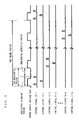
With reference to FIGS. 5 and 6, a conventional sensor and
a driving method thereof will be described. FIG. 5 is a circuit
diagram of a conventional sensor. The sensor shown in FIG. 5 has
photosensitive cells (the portions surrounded by dotted-lines)
arranged in a 2 x 2 matrix form. Each photosensitive cell includes
a photodiode 51, a transfer gate 52, a floating diffusion layer
portion 53, an amplifying transistor 54, a reset transistor 55,
and an address transistor 56, and corresponds to one of the pixels
composing an image. Note that although the following description
will assume, for simplicity, that the photosensitive cells are
arranged in a 2 x 2 matrix form, in practice, several tens to several
thousands of photosensitive cells are arranged in each of the row
and column directions.
-
A method of driving the sensor shown in FIG. 5 is as follows.
To extract signals from photosensitive cells in the first row,
first, address transistors 56a and 56b included in the
photosensitive cells in the first row are controlled to be in an
ON state by a vertical shift register 61. Then, reset transistors
55a and 55b are similarly controlled to be in an ON state by the
vertical shift register 61. This resets floating diffusion layer
portions 53a and 53b. At this stage, an amplifying transistor
54a and a load transistor 63p form a source follower circuit, and
an output from the source follower circuit appears on a vertical
signal line 62p. Similarly, an amplifying transistor 54b and a
load transistor 63q form a source follower circuit, and an output
from the source follower circuit appears on a vertical signal line
62q as well. Voltages appearing on the vertical signal lines 62p
and 62q at this stage are noise voltages which are unrelated to
signal charges accumulated in photodiodes 51a and 51b.
Subsequently, transfer gates 52a and 52b are controlled to be in
an ON state by the vertical shift register 61. By this, the signal
charges accumulated in the photodiodes 51a and 51b are transferred
to the floating diffusion layer portions 53a and 53b, and signal
voltages corresponding to the signal charges accumulated in the
photodiodes 51a and 51b appear on the vertical signal lines 62p
and 62q.
-
Clamp capacitors 64p and 64q, clamp transistors 65p and 65q,
sample/ hold transistors 66p and 66q, and sample/ hold capacitors
67p and 67q forma noise suppression circuit. The noise suppression
circuit determines the difference between a pixel output obtained
when there are signal charges in the floating diffusion layer
portions 53 (i.e., a signal output) and a pixel output obtained
when there is no signal charge (i.e., a noise output). In the
sensor shown in FIG. 5, mainly, noise caused by variations in the
threshold voltages of the amplifying transistors 54 and kTC noise
which is the thermal noise of the reset transistors 55 are generated.
When noise outputs are appearing on the vertical signal lines 62p
and 62q, the clamp transistors 65p and 65q and the sample/ hold
transistors 66p and 66q are controlled to be in an ON state through
control terminals 74 and 75, and a noise-free clamp voltage is
applied to the sample/ hold capacitors 67p and 67q from a clamp
voltage supply terminal 73. After a predetermined time has elapsed,
the clamp transistors 65p and 65q are controlled to be in an OFF
state through the control terminal 74.
-
Subsequently, a voltage equal to the sum of a noise-free
signal voltage and a noise voltage appears on each of the vertical
signal lines 62p and 62q. The vertical signal lines 62p and 62q
each change from the noise voltage to the sum of the signal voltage
and the noise voltage; the amount of the change is equal to the
noise-free signal voltage. Therefore, the voltage of each of the
clamp capacitors 64p and 64q on the sample/hold side also changes
by an amount equal to the noise-free signal voltage. In practice,
the voltage across each of the sample/ hold capacitors 67p and 67q
changes from the noise-free clamp voltage by an amount obtained
by dividing the amount of signal voltage change on the corresponding
vertical signal line 62p or 62q by a corresponding clamp capacitor
and a corresponding sample/hold capacitor. Therefore, the
voltage across each of the sample/ hold capacitors 67p and 67q is
the noise-free clamp voltage and the divided signal voltage, and
the noise portion is removed. After the sample/ hold transistors
66p and 66q are controlled to be in an OFF state, horizontal
transistors 68p and 68q are sequentially and selectively controlled
to be in an ON state by a horizontal shift register 69. By this,
signals corresponding to the signal charges accumulated in the
photodiodes 51a and 51b are sequentially outputted from an output
terminal 70.
-
Next, to extract signals from photosensitive cells in the
second row, the same operations as for the first row are performed
on the photosensitive cells in the second row. By this, signals
corresponding to signal charges accumulated in photodiodes 51c
and 51d are sequentially outputted from the output terminal 70.
-
A timing chart showing the above-described operations is
as shown in FIG. 6. In FIG. 6, the period during which signals
accumulated in photodiodes 51 for one row are finally outputted
from the output terminal 70 is called a horizontal effective period,
and the period during which the signals are outputted from the
photodiodes 51 to the vertical signal lines 62 and the noise of
the outputted signals is suppressed is called a horizontal blanking
period. The horizontal blanking period and the horizontal
effective period are together called one horizontal period. The
one horizontal period is the time actually required to read signals
for one row. The time required to read signals from the entire
sensor is called one frame period. As shown in FIG. 6, the amount
of a signal charge accumulated in the photodiode 51 is determined
by the time interval of a transfer pulse to be applied to the transfer
gate 52. The time interval of the transfer pulse is constant during
one frame period. Therefore, the photodiodes 51 have uniform
sensitivity.
-
In the sensor shown in FIG. 5, each photosensitive cell is
composed of four transistors (a transfer gate 52, an amplifying
transistor 54, a reset transistor 55, and an address transistor
56). On the other hand, in recent years, for reduction in size
of sensors, there has developed a sensor having photosensitive
cells each composed of three transistors. This newly developed
sensor has a configuration in which address transistors 56 are
removed from the sensor shown in FIG. 5 and the power supply is
shared between the photosensitive cells. In order to read signals
from this sensor, it is necessary to supply a pulsed power supply
voltage to each photosensitive cell.
-
A method of driving the sensor shown in FIG. 5 is described
in Japanese Laid-Open Patent Publication No. 9-247537, for example.
In addition, Japanese Laid-Open Patent Publication No. 2001-45375
describes a driving method by which signals from photodiodes for
one row are averagely outputted in one horizontal period.
-
However, in the sensor in which each photosensitive cell
is composed of three transistors, because the power supply is
pulse-driven, problems such as those described below may arise.
First, since the power supply is connected to all the photosensitive
cells and not only a selected photosensitive cell but the entire
sensor is driven, adverse effects are exerted on the operation
of the entire sensor. Secondly, although the power supply voltage
at a high level does not exert adverse effects on the operation
of the sensor, the power supply voltage at a low level exerts adverse
effects on the operation of a non-selected photosensitive cell.
Thirdly, pulse-driving of the power supply per se exerts various
adverse effects on the entire sensor.
-
Inparticular, in terms of the aforementioned secondproblem,
if the low-level potential of the power supply becomes too low,
this low-level potential may become equal to or lower than the
low-level potential of the reset transistors of non-selected
photosensitive cells and reach even to the gate regions of
amplifying transistors. Here, a large number of amplifying
transistors simultaneously go into operation and drive the entire
sensor. Accordingly, a great noise is superimposed during a
horizontal blanking period, and thereby signal processing becomes
difficult.
-
If the low-level potential of the power supply becomes equal
to or lower than the low-level potential of the transfer gates
of non-selected photosensitive cells, charges are injected into
photodiodes, causing variations in the amount of charge injected
into the photosensitive cells. Accordingly, variations occur in
signal charges to be read from the photodiodes and thereby a great
noise appears in a reproduced image.
-
Therefore, an object of the present invention is to provide
a method of driving a solid-state imaging device, by which a
reproduced image with low noise is read from a sensor having
photosensitive cells each composed of three transistors.
DISCLOSURE OF THE INVENTION
-
To achieve the above objects, the present invention has the
following aspects.
-
A first aspect of the present invention is directed to a
method of driving a solid-state imaging device comprising: a
photosensitive region having photosensitive cells arranged
two-dimensionally in row and column directions on a semiconductor
substrate, each photosensitive cell including a photodiode for
accumulating a signal charge obtained by converting incoming light
into electricity; a transfer transistor for transferring the signal
charge accumulated in the photodiode; a floating diffusion layer
portion for temporarily accumulating the transferred signal
charge; an amplifying transistor for amplifying the signal charge
accumulated in the floating diffusion layer portion; and a reset
transistor for resetting the signal charge accumulated in the
floating diffusion layer portion; a power supply line commonly
connected to drains of the amplifying transistors; a vertical
driver circuit for individually driving transfer transistors
arranged in a same row and reset transistors arranged in the same
row; a plurality of vertical signal lines each having commonly
connected thereto corresponding amplifying transistors arranged
in a same column; a plurality of load transistors connected to
the vertical signal lines, respectively; a noise suppression
circuit for suppressing noise of signals outputted to the vertical
signal lines; a plurality of horizontal transistors which are
arranged in the row direction, and to which outputs from the noise
suppression circuit are inputted; and a horizontal driver circuit
for allowing the horizontal transistors to sequentially and
selectively operate, and thereby sequentially outputting the
outputs from the noise suppression circuit, the method comprising
the steps of : pulse-driving the power supply line on a per horizontal
period basis; sequentially selecting different rows on a per
horizontal period basis using the horizontal driver circuit, and
allowing corresponding reset transistors and corresponding
transfer transistors included in corresponding photosensitive
cells arranged in a selected row to successively operate while
the power supply line is driven, and thereafter allowing the
corresponding reset transistors to operate while the power supply
line is not driven; and sequentially outputting outputs from the
noise suppression circuit on a per horizontal period basis using
the horizontal driver circuit, wherein a low-level potential of
the power supply line has a predetermined potential higher than
zero potential.
-
According to the method of driving the solid-state imaging
device, by making the low-level potential of the power supply line
higher than zero potential, it is possible to prevent the entire
sensor from being driven and to stabilize the potential of each
pixel. Accordingly, a reproduced image with low noise can be read.
-
In the method of driving the solid-state imaging device,
the predetermined potential may be higher than channel potentials
obtained when a low level is applied to the reset transistors.
By doing so, the amplifying transistors are prevented from
operating in the vicinity of their respective gate regions, and
thus it is possible to prevent a situation where a large number
of amplifying transistors simultaneously go into operation and
as a result the entire sensor is driven. Accordingly, it is
possible to solve a problem that a great noise is superimposed
during a horizontal blanking period, and thereby signal processing
becomes difficult.
-
Alternatively, the predetermined potential may be higher
than channel potentials obtained when a low level is applied to
the transfer transistors. By doing so, it is possible to prevent
a situation where because of the charges injected into the
photodiodes, variations in the amount of charge to be injected
occur in the photosensitive cells. Accordingly, a beautifully
reproduced image with low noise can be read without causing a great
noise to appear in the reproduced image.
-
Alternatively, the predetermined potential may be higher
than channel potentials of the photodiodes. By doing so, it is
possible to prevent the entire sensor from being driven and to
stabilize the potential of each pixel. Accordingly, a reproduced
image with low noise can be read.
-
In the method of driving the solid-state imaging device,
the photosensitive region may be formed on a p-type substrate.
By doing so, a reproduced image with low noise can be read from
a solid-state imaging device having a photosensitive region formed
on a p-type substrate.
-
Alternatively, the photosensitive region may be formed in
a p-type well on an n-type substrate. By doing so, a reproduced
image with low noise can be read from a solid-state imaging device
having a photosensitive region formed in a p-type well on an n-type
substrate.
BRIEF DESCRIPTION OF THE DRAWINGS
-
- FIG. 1 is a circuit diagram of a sensor according to an
embodiment of the present invention.
- FIGS. 2A and 2B are diagrams showing the details of a noise
suppression circuit of the sensor according to the embodiment of
the present invention.
- FIG. 3 is a timing chart showing a method of driving the
sensor according to the embodiment of the present invention.
- FIGS. 4A and 4B are a cross-sectional view and a potential
diagram of a photosensitive cell of the sensor according to the
embodiment of the present invention.
- FIG. 5 is a circuit diagram of a conventional sensor.
- FIG. 6 is a timing chart showing a method of driving the
conventional sensor.
-
BEST MODE FOR CARRYING OUT THE INVENTION
-
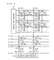
FIG. 1 is a circuit diagram of a sensor according to an
embodiment of the present invention. The sensor shown in FIG.
1 has photosensitive cells (the portions surrounded by
dotted-lines) arranged in an m × n matrix form; a power supply
line 10; a vertical shift register 11; n vertical signal lines
12-1 to 12-n; n load transistors 13-1 to 13-n; a noise suppression
circuit 14; n horizontal transistors; and a horizontal shift
register 16. Each photosensitive cell includes a photodiode 1,
a transfer gate 2, a floating diffusion layer portion 3, an
amplifying transistor 4, and a reset transistor 5. The
photosensitive cell is characterized in that it includes three
transistors (the transfer gate 2, the amplifying transistor 4,
and the reset transistor 5) and does not include an address
transistor. The values of m and n in an actual sensor are in the
order of from several tens to several thousands.
-
The m × n photosensitive cells are formed on a semiconductor
substrate. More specifically, the photosensitive cells are
formed on a p-type substrate or in a p-well on an n-type substrate.
In each photosensitive cell, the photodiode 1 converts incoming
light into electricity and accumulates therein an obtained signal
charge. The transfer gate 2 is provided between the photodiode
1 and the floating diffusion layer portion 3, and transfers the
signal charge accumulated in the photodiode 1 to the floating
diffusion layer portion 3. The floating diffusion layer portion
3 temporarily accumulates therein the signal charge transferred
from the photodiode 1. The amplifying transistor 4 amplifies the
signal charge accumulated in the floating diffusion layer portion
3. The reset transistor 5 resets the signal charge accumulated
in the floating diffusion layer portion 3.
-
In a photosensitive region where the photosensitive cells
are arranged, pairs of m signals lines 17-1 to 17-m and 18-1 to
18-m are wired in addition to the power supply line 10 and the
vertical signal lines 12-1 to 12-n. The power supply line 10 is
commonly connected to drains of the amplifying transistors 4. The
present embodiment assumes that the power supply line 10 is commonly
connected to the drains of the amplifying transistors 4 and the
reset transistors 5 included in all the photosensitive cells, and
a pulsed power supply voltage VddC is applied to all the
photosensitive cells from a power supply terminal 20 which is
present at the other end of the power supply line 10. Note that
although, in FIG. 1, all the photosensitive cells are connected
to the single power supply line 10, two or more power supply lines
may be used to supply a common power supply to the photosensitive
cells.
-
Each of the vertical signal lines 12-1 to 12-n is provided
to a corresponding column of photosensitive cells. The vertical
signal lines 12-1 to 12-n connect between corresponding amplifying
transistors 4 included in photosensitive cells and corresponding
load transistors 13-1 to 13-n, which are arranged in the same column,
and the noise suppression circuit 14. The signal lines 17-1 to
17-m and 18-1 to 18-m are output signal lines of the vertical shift
register 11, and are each provided to a corresponding row of
photosensitive cells. The signal lines 17-1 to 17-m connect
between gates of corresponding transfer gates 2 included in
photosensitive cells arranged in the same row. The signal lines
18-1 to 18-m connect between gates of corresponding reset
transistors 5 included in photosensitive cells arranged in the
same row.
-
The vertical shift register 11 operates as a vertical driver
circuit as described below. When the power supply line VddC is
at a high level, the vertical shift register 11 simultaneously
drives corresponding transfer gates 2 included in photosensitive
cells arranged in the same row. In addition, when the power supply
line VddC is at a high level, the vertical shift register 11
simultaneously drives corresponding reset transistors 5 included
in photosensitive cells arranged in the same row, at a different
timing than the drive timing of the transfer gates 2. The load
transistors 13-1 to 13-n are connected to the vertical signal lines
12-1 to 12-n, respectively, and arranged in the row direction.
The noise suppression circuit 14 is connected to the vertical signal
lines 12-1 to 12-n, and captures signals outputted from the
amplifying transistors 4 and then removes the noise component in
the captured signals. Horizontal transistors 15-1 to 15-n are
arranged in the row direction. To the horizontal transistors 15-1
to 15-n are inputted n signals outputted from the noise suppression
circuit 14, respectively. The horizontal shift register 16
operates as a horizontal driver circuit. Specifically, the
horizontal shift register 16 allows the horizontal transistors
15-1 to 15-n to sequentially and selectively operate. By doing
so, the n signals outputted from the noise suppression circuit
14 are sequentially outputted from the output terminal 21.
-
FIGS. 2A and 2B are diagrams for describing the details of
the noise suppression circuit 14. The noise suppression circuit
14 includes, as shown in FIGS. 2A, n sample/hold transistors 31-1
to 31-n; n clamp capacitors 32-1 to 32-n; n clamp transistors 33-1
to 33-n; and n sample/hold capacitors 34-1 to 34-n. The noise
suppression circuit 14 is different from the noise suppression
circuit shown in FIG. 5 in the position of the sample/hold
transistors 31-1 to 31-n, but operates substantially in the same
manner as the noise suppression circuit shown in FIG. 5. A
sample/hold control signal inputted from a control terminal 22
is applied to gates of the sample/hold transistors 31-1 to 31-n.
Similarly, a clamp control signal inputted from a control terminal
23 is applied to gates of the clamp transistors 33-1 to 33-n. These
two control signals change as shown in FIG. 2B. A period during
which both of the two control signals are at a high level serves
as a noise output period, and a period during which the sample/hold
control signal is at a high level and the clamp control signal
is at a low level serves as a signal output period.
-
With reference to a timing chart shown in FIG. 3, where
appropriate, a method of driving the sensor shown in FIG. 1 will
be described below. To drive the sensor, there are performed a
step of pulse-driving the power supply line 10 on a per horizontal
period basis; a step of reading signals for one row from the
m × n photodiodes 1 using the vertical shift register 11; and
a step of sequentially outputting the read signals for one row
using the horizontal shift register 16.
-
As shown in FIG. 3, in an initial state, a power supply voltage
VddC is at a low level. That is, in the initial state, the power
supply line 10 is not yet driven. To extract signals from the
photosensitive cells in the first row, first, the power supply
voltage VddC is controlled to be at a high level. By this, in
all the photosensitive cells, the drains of the transfer gates
2 and the reset transistors 5 are brought to a high level. Then,
while the power supply line 10 is driven, the vertical shift register
11 brings the signal line 18-1 to a high level for a predetermined
period of time. By this, the gate potentials of the reset
transistors 5a and 5b and all other reset transistors 5 included
in the photosensitive cells in the first row are brought to a high
level, and these reset transistors 5 are brought into an ON state.
At this stage, the amplifying transistors 4a and 4b and all other
amplifying transistors 4 included in the photosensitive cells in
the first row are brought into an operation state. At the same
time, noise outputs, which are generated when signal charges
accumulated in the floating diffusion layer portions 3a and 3b
and all other floating diffusion layer portions 3 included in the
photosensitive cells in the first row are reset, appear on the
vertical signal lines 12-1 to 12-n.
-
Subsequently, while the power supply line 10 is driven, the
vertical shift register 11 brings the signal line 17-1 to a high
level for a predetermined period of time. By this, the gate
potentials of the transfer gates 2a and 2b and all other transfer
gates 2 included in the photosensitive cells in the first row are
brought to a high level, and these transfer gates 2 are brought
into an ON state. At this stage, signal charges accumulated in
the photodiodes 1a and 1b and all other photodiodes 1 included
in the photosensitive cells in the first row are read into
corresponding floating diffusion layer portions 3 included in the
photosensitive cells, and then signal outputs corresponding to
the read signal charges appear on the vertical signal lines 12-1
to 12-n.
-
In this manner, on each of the vertical signal lines 12-1
to 12-n, after a noise voltage appears, the sum of a signal voltage
and the noise voltage appears. The noise suppression circuit 14
operates in the same manner as the conventional noise suppression
circuit, and suppresses the noise of the signals outputted to the
vertical signal lines 12-1 to 12-n. The n signals outputted from
the noise suppression circuit 14 are inputted to the horizontal
transistors 15-1 to 15-n, respectively.
-
After the noise suppression circuit 14 goes into operation,
the power supply voltage VddC changes to a low level. Then, while
the power supply line 10 is not driven, the vertical shift register
11 brings the signal line 18-1 to a high level for a predetermined
periodoftime. By this, signal charges accumulated in the floating
diffusion layer portions 3a and 3b and all other floating diffusion
layer portions 3 included in the photosensitive cells in the first
row are reset. The amplifying transistors 4a and 4b and all other
amplifying transistors 4 included in the photosensitive cells in
the first row remain in a non-operation state until they are selected
again.
-
The horizontal shift register 16 outputs n output signals
connected to the gates of the horizontal transistors 15-1 to 15-n.
The horizontal shift register 16 selectively brings the n output
signals to a high level, and thereby sequentially and selectively
controls the horizontal transistors 15-1 to 15-n to be in an ON
state. By this, signals corresponding to the signal charges
accumulated in the photodiodes 1a and 1b and all other photodiodes
1 in the first row are sequentially outputted from the output
terminal 21.
-
Then, to extract signals from the photosensitive cells in
the second row, the same operations as for the fist row are performed
on the photosensitive cells in the second row. By this, signals
corresponding to signal charges accumulated in the photodiodes
1c and 1d and all other photosensitive cells in the second row
are sequentially outputted from the output terminal 21.
Thereafter, the same operations are performed on photosensitive
cells from the third to the m-th rows. Note that the definitions
of a horizontal blanking period, a horizontal effective period,
one horizontal period, and one frame period shown in FIG. 3 and
the fact that the photodiodes 1 have uniform sensitivity, are the
same as those for the conventional sensor.
-
Of methods of driving a sensor, such as that described above,
the present embodiment considers a driving method which is
characterized in that the low-level potential of a power supply
voltage VddC is a predetermined potential higher than zero
potential. Specifically, there are considered a driving method
in which the low-level potential of the power supply voltage VddC
is higher than the channel potentials obtained when a low level
is applied to reset transistors 5, and a driving method in which
the low-level potential of the power supply voltage VddC is higher
than the channel potentials obtained when a low level is applied
to transfer gates 2. According to the driving methods having such
characteristics, a reproduced image having less noise than that
obtained by conventional driving methods can be obtained. The
reasons will be described below with reference to FIGS. 4A and
4B.
-
FIGS. 4A and 4B are respectively a cross-sectional view and
a potential diagram of a photosensitive cell included in the sensor
shown in FIG. 1. In FIG. 4A, the photosensitive cell is formed
on a p-type substrate. The p-type substrate, an n-type photodiode
layer 41 formed on the p-type substrate, and a p-type surface layer
42 formed on a surface of the p-type substrate, compose a photodiode
1. In addition to the photodiode 1, a floating diffusion layer
portion 3 and an n-type surface layer 45 are formed on the p-type
substrate. Upon this, by providing an electrode 43 a transfer
gate 2 is formed, and by providing an electrode 44 a reset transistor
5 is formed.
-
As described above, the power supply voltage VddC changes
in pulse form. Here, the high-level potential and low-level
potential of the power supply voltage VddC are noted as VddC_H
and VddC_L, respectively (see FIG. 4B). The actual value of VddC_H
is 2.8 V, for example. A voltage which varies within a range from
0 V to 2.8 V is applied to the gates of the reset transistors 5;
the channel potentials obtained when a low-level potential (0 V)
is applied to the gates of the reset transistors 5 are noted as
TRchL. A voltage which varies in a range from 0 V to 2.8 V is
also applied to the gates of the transfer gates 2; the channel
potentials obtained when a low-level potential (0 V) is applied
to the gates of the transfer gates 2 are noted as TRchL. With
the use of the notation, in the present embodiment, the low-level
potential VddC_L of the power supply voltage is controlled such
that the following relationship(s) holds:
RSchL < VddC_L
and/or
TRchL < VddC_L
-
The use of a low-level potential VddC_L for which the
aforementioned expression (1) holds, prevents the amplifying
transistors 4 from operating in the vicinity of their respective
gate regions. Thus, a phenomenon does not occur in which a large
number of amplifying transistors 4 simultaneously go into operation
and as a result the entire sensor is driven. Accordingly, it is
possible to solve a problem that a great noise is superimposed
during a horizontal blanking period, and thereby signal processing
becomes difficult.
-
The use of a low-level potential VddC_L for which the
aforementioned expression (2) holds, prevents a phenomenon from
occurring in which because of the charges injected into the
photodiodes 1 variations in the amount of charge to be injected
occur in the photosensitive cells. Accordingly, it is possible
to read a beautifully reproduced image without causing a great
noise to appear in the reproduced image.
-
As described above, by using a low-level potential VddC_L
of the power supply voltage for which the aforementioned
expression(s) (1) and/or (2) holds, the entire sensor is not driven
and the potential of each pixel is stabilized, and therefore it
is possible to read a beautifully reproduced image with low noise.
-
Note that, in practice, in place of the aforementioned
expressions (1) and (2), or in addition to the aforementioned
expression(s) (1) and/or (2), as the low-level potential VddC_L
of the power supply voltage, a potential higher than the channel
potentials of photodiodes may be used. In the case of using such
a potential, a reproduced image with low noise can be read from
the sensor shown in FIG. 1 as well.
-
For a sensor to which the driving method according to the
present embodiment is applicable, a sensor formed on a p-type
substrate, as shown in FIG. 4A, may be used or a sensor formed
on a p-well in an n-type substrate may be used. The driving method
according to the present embodiment is applicable to a sensor formed
by either method.
INDUSTRIAL APPLICABILITY
-
As described above, the method of driving a solid-state
imaging device according to the present invention has
characteristics in that a reproduced image with low noise can be
read, and thus can be used as a driving method by which a reproduced
image is read from various solid-state imaging devices.