EP1594191B1 - Adaptor device for electronic device - Google Patents
Adaptor device for electronic device Download PDFInfo
- Publication number
- EP1594191B1 EP1594191B1 EP04700530A EP04700530A EP1594191B1 EP 1594191 B1 EP1594191 B1 EP 1594191B1 EP 04700530 A EP04700530 A EP 04700530A EP 04700530 A EP04700530 A EP 04700530A EP 1594191 B1 EP1594191 B1 EP 1594191B1
- Authority
- EP
- European Patent Office
- Prior art keywords
- card
- adapter device
- electronic equipment
- loading
- host equipment
- Prior art date
- Legal status (The legal status is an assumption and is not a legal conclusion. Google has not performed a legal analysis and makes no representation as to the accuracy of the status listed.)
- Expired - Fee Related
Links
Images


Classifications
-
- G—PHYSICS
- G06—COMPUTING; CALCULATING OR COUNTING
- G06K—GRAPHICAL DATA READING; PRESENTATION OF DATA; RECORD CARRIERS; HANDLING RECORD CARRIERS
- G06K19/00—Record carriers for use with machines and with at least a part designed to carry digital markings
- G06K19/06—Record carriers for use with machines and with at least a part designed to carry digital markings characterised by the kind of the digital marking, e.g. shape, nature, code
- G06K19/067—Record carriers with conductive marks, printed circuits or semiconductor circuit elements, e.g. credit or identity cards also with resonating or responding marks without active components
- G06K19/07—Record carriers with conductive marks, printed circuits or semiconductor circuit elements, e.g. credit or identity cards also with resonating or responding marks without active components with integrated circuit chips
- G06K19/077—Constructional details, e.g. mounting of circuits in the carrier
- G06K19/07743—External electrical contacts
-
- H—ELECTRICITY
- H01—ELECTRIC ELEMENTS
- H01R—ELECTRICALLY-CONDUCTIVE CONNECTIONS; STRUCTURAL ASSOCIATIONS OF A PLURALITY OF MUTUALLY-INSULATED ELECTRICAL CONNECTING ELEMENTS; COUPLING DEVICES; CURRENT COLLECTORS
- H01R12/00—Structural associations of a plurality of mutually-insulated electrical connecting elements, specially adapted for printed circuits, e.g. printed circuit boards [PCB], flat or ribbon cables, or like generally planar structures, e.g. terminal strips, terminal blocks; Coupling devices specially adapted for printed circuits, flat or ribbon cables, or like generally planar structures; Terminals specially adapted for contact with, or insertion into, printed circuits, flat or ribbon cables, or like generally planar structures
- H01R12/70—Coupling devices
- H01R12/71—Coupling devices for rigid printing circuits or like structures
-
- G—PHYSICS
- G06—COMPUTING; CALCULATING OR COUNTING
- G06K—GRAPHICAL DATA READING; PRESENTATION OF DATA; RECORD CARRIERS; HANDLING RECORD CARRIERS
- G06K19/00—Record carriers for use with machines and with at least a part designed to carry digital markings
- G06K19/06—Record carriers for use with machines and with at least a part designed to carry digital markings characterised by the kind of the digital marking, e.g. shape, nature, code
- G06K19/067—Record carriers with conductive marks, printed circuits or semiconductor circuit elements, e.g. credit or identity cards also with resonating or responding marks without active components
- G06K19/07—Record carriers with conductive marks, printed circuits or semiconductor circuit elements, e.g. credit or identity cards also with resonating or responding marks without active components with integrated circuit chips
- G06K19/077—Constructional details, e.g. mounting of circuits in the carrier
- G06K19/0772—Physical layout of the record carrier
- G06K19/07732—Physical layout of the record carrier the record carrier having a housing or construction similar to well-known portable memory devices, such as SD cards, USB or memory sticks
-
- G—PHYSICS
- G06—COMPUTING; CALCULATING OR COUNTING
- G06K—GRAPHICAL DATA READING; PRESENTATION OF DATA; RECORD CARRIERS; HANDLING RECORD CARRIERS
- G06K19/00—Record carriers for use with machines and with at least a part designed to carry digital markings
- G06K19/06—Record carriers for use with machines and with at least a part designed to carry digital markings characterised by the kind of the digital marking, e.g. shape, nature, code
- G06K19/067—Record carriers with conductive marks, printed circuits or semiconductor circuit elements, e.g. credit or identity cards also with resonating or responding marks without active components
- G06K19/07—Record carriers with conductive marks, printed circuits or semiconductor circuit elements, e.g. credit or identity cards also with resonating or responding marks without active components with integrated circuit chips
- G06K19/077—Constructional details, e.g. mounting of circuits in the carrier
- G06K19/07737—Constructional details, e.g. mounting of circuits in the carrier the record carrier consisting of two or more mechanically separable parts
- G06K19/07741—Constructional details, e.g. mounting of circuits in the carrier the record carrier consisting of two or more mechanically separable parts comprising a first part operating as a regular record carrier and a second attachable part that changes the functional appearance of said record carrier, e.g. a contact-based smart card with an adapter part which, when attached to the contact card makes the contact card function as a non-contact card
-
- H—ELECTRICITY
- H01—ELECTRIC ELEMENTS
- H01R—ELECTRICALLY-CONDUCTIVE CONNECTIONS; STRUCTURAL ASSOCIATIONS OF A PLURALITY OF MUTUALLY-INSULATED ELECTRICAL CONNECTING ELEMENTS; COUPLING DEVICES; CURRENT COLLECTORS
- H01R12/00—Structural associations of a plurality of mutually-insulated electrical connecting elements, specially adapted for printed circuits, e.g. printed circuit boards [PCB], flat or ribbon cables, or like generally planar structures, e.g. terminal strips, terminal blocks; Coupling devices specially adapted for printed circuits, flat or ribbon cables, or like generally planar structures; Terminals specially adapted for contact with, or insertion into, printed circuits, flat or ribbon cables, or like generally planar structures
- H01R12/70—Coupling devices
- H01R12/71—Coupling devices for rigid printing circuits or like structures
- H01R12/72—Coupling devices for rigid printing circuits or like structures coupling with the edge of the rigid printed circuits or like structures
- H01R12/721—Coupling devices for rigid printing circuits or like structures coupling with the edge of the rigid printed circuits or like structures cooperating directly with the edge of the rigid printed circuits
-
- H—ELECTRICITY
- H01—ELECTRIC ELEMENTS
- H01R—ELECTRICALLY-CONDUCTIVE CONNECTIONS; STRUCTURAL ASSOCIATIONS OF A PLURALITY OF MUTUALLY-INSULATED ELECTRICAL CONNECTING ELEMENTS; COUPLING DEVICES; CURRENT COLLECTORS
- H01R31/00—Coupling parts supported only by co-operation with counterpart
- H01R31/06—Intermediate parts for linking two coupling parts, e.g. adapter
Definitions
- the present invention relates to an adapter device for electronic equipment which can load another electronic equipment with respect to a loading unit of an electronic equipment such as existing IC card, etc.
- substantially plate-shaped IC cards within which semiconductor integrated circuit elements are included.
- the IC card includes a substantially rectangular card body within which, e.g., flash memory is included, wherein terminal portions for electrically connecting to host equipment are provided at one short side of the card body.
- a loading portion adapted so that small-sized IC card is loaded therewithin is provided, an insertion/withdrawal opening for the small-sized IC card is provided at the rear surface side in a manner continuous to the loading portion, and terminal portions for performing electrical connection to the host equipment are provided at the front surface side.
- cut portions are provided at both corner portions of the rear surface side where insertion/withdrawal portion is provided.
- the cut portions provided at both corner portions of the rear surface side where the insertion/withdrawal portion is provided allow both corner portions of the rear surface side of the IC card to be faced to the external when the small-sized IC card is loaded with respect to the loading portion to permit user to grasp the portion faced to the external portion from the cut portions of the IC card, e.g., both side surfaces of the rear surface side to take out the IC card loaded at the loading portion from the loading portion.
- both corner portions of the rear surface side of the small-sized IC card loaded at the loading portion are only faced to the external portion from the cut portions at the time of loading of the small-sized IC card, the area that user can grasp the small-sized IC card is small.
- user takes out the small-sized IC card from the loading portion he draws out the IC card loaded at the loading portion in such a manner to grasp side surfaces opposite to each other of the rear surface side of the IC card faced to the external from the cut portions. Since the area that user grasps the IC card is narrow, it becomes difficult to draw or pull out the IC card.
- portions of the top face and/or the lower face of the IC card are used as memorandum area for memorizing the content, etc. of data that user preserves onto the IC card.
- the memorandum area is used as area where memorandum is described directly by using pen on the casing by user, and/or is used as an area where label for describing as memorandum is stuck. Namely, label that user has described as memorandum or user intends to describe as memorandum is stuck.
- the adapter device described in the pamphlet when the small-sized IC card is loaded with respect to the loading portion, the entirety of the small-sized IC card is covered by the casing except for both corner portions of the rear surface side where cut portions are provided.
- the top face of the adapter device is the portion noticed for user to the greatest degree, and is extremely important area in design. Accordingly, it is desirable that the configurations indispensable in view of function of the adapter device are provided at the lower face side if possible, and the top face can be freely designed if possible.
- US-A-5993261 discloses an adapter for connecting cards to a computing device. It has substantially identical grip recesses in the top and bottom surfaces and a cut out portion which provides a surface to help enable a user to extract the adapter from the host device. When inserted into the adapter card protrudes out of the adapter by a substantial amount.
- An object of the present invention is to provide a novel adapter device for electronic equipment which can solve problems that prior arts as described above have.
- Another object of the present invention is to provide an adapter device for electronic equipment which makes it possible to easily perform take-out operation of electronic equipment to realize improvement in operability.
- a further object of the present invention is to provide an adapter device for electronic equipment which can visually recognize memorandum area provided at an electronic equipment even at the time of loading to thereby realize improvement in operability.
- a still further object of the present invention is to provide an adapter device for electronic equipment in which design of outer appearance is caused to become satisfactory.
- the adapter device 30 is loaded at a loading portion within a host equipment 1 through an insertion opening 2 provided at the host equipment 1 in the state where there is loaded an IC card 10 in which there is included semiconductor memory used as external memory unit for host equipment 1 such as recording and/or reproducing apparatus for audio data, personal computer, digital still camera and/or digital video camera, etc.
- the adapter device 30 is formed so as to have substantially the same size as the existing IC card, and is adapted for permitting IC card 10 smaller than IC card conventionally used to be loaded at host equipment 1 having loading portion corresponding to IC card conventionally used.
- the adapter device 30 includes a casing 31 constituting the device body, wherein the IC card 10 is loaded into the casing 31.
- This IC card 10 is common to the existing IC card in the electric specification, and is different from the latter in the physical specification. In concrete terms, the IC card 10 is miniaturized so that its long side is caused to be shorter than long side of the existing IC card.
- the IC card 10 comprises, as shown in FIGS. 4 and 5 , a substantially rectangular plate-shaped card body 11 obtained by molding synthetic resin material.
- semiconductor memory elements such as flash memory, etc. having large memory capacity of 4 MB (mega bytes) or more, e.g., 4 MB, 16 MB, 32 MB, 64 MB, 128 MB, 256 MB or 1 GB, control circuit elements in which control circuit portions for controlling write operation of data such as audio data, etc. with respect to the semiconductor memory elements, or read-out operation of data such as audio data, etc. stored in the semiconductor memory elements, and plural semiconductor integrated circuit elements such as copyright protection circuit elements, etc. in the state where they are mounted on a printed wiring board.
- the card body 11 in which plural semiconductor elements are included as stated above and the printed wiring board on which these semiconductor elements are mounted is included is formed so as to have mechanical strength to such a degree that it is not bent by ordinary external force applied at the time of use, etc. thus to realize protection of included semiconductor elements such as semiconductor memory elements, etc. and the printed wiring board on which these semiconductor elements are mounted.
- the card body 11 is formed by molded body of synthetic resin.
- the IC card 10 is common to the IC card of the standard use already used in the electrical specification, but is different from the latter in the physical specification.
- the IC card 10 is adapted so that the outside configuration is miniaturized to more degree as compared to the standard IC card.
- the card body 11 is formed as rectangular shape in which length W of the short side is caused to be substantially 20 mm, length L of the long side is caused to be substantially 31 mm, and the thickness T is caused to be substantially 1.6 mm.
- the IC card of the standard size is similar to the above-described IC card 10 in the fundamental specification, but is different from the latter only in the size thereof.
- the IC card of the standard size is formed as rectangular shape in which length W of the short side is caused to be substantially 21.45 mm, length L of the long side is caused to be substantially 50 mm, and thickness T is caused to be substantially 2.8 mm.
- a terminal portion 12 in a manner extending from front surface 11a serving as insertion end into the host equipment toward bottom surface 11b.
- the terminal portion 12 there are provided plural engagement recessed portions 14 partitioned by partition walls 13 in correspondence with the number of electrodes 15.
- the respective engagement recessed portions 14 are opened in a manner extending from the front surface 11 a of the card body 11 toward the bottom surface 11b thereof so that a group of terminals provided at the loading portion side of the host equipment can be engaged thereinto.
- the plural electrodes 15 are provided in the state where they are respectively positioned at the bottom surfaces of the respective engagement recessed portions 14, and are separated from each other by the partition walls 13.
- plural respective electrodes 15 are respectively provided at the bottom surfaces of the engagement recessed portions 14 partitioned so that they are smaller than size of finger of the human being by partition walls 13, finger and/or large foreign material are prevented from directly being coming into contact with the IC card 10 at the time of handling thereof.
- the IC card 10 is securely protected from stain and/or damage, etc.
- at least electrodes 15 are used as at least input termonal for serial protocol bus state signal BS, input terminal for serial protocol data signal SDIO, input terminal for serial clock SCLK, and power supply voltage VCC terminal. It is a matter of course that transmission/reception of data to and from the host equipment may be performed by parallel interface.
- inclination surface portions 16 are formed, as shown in FIG. 5 , inclination surface portions 16 in a manner extending from the middle portion in the thickness direction of the front surface 11 a of the card body 11 toward the bottom surface 11b thereof.
- the inclination surface portion 16 functions as an insertion guide portion when the IC card 10 is inserted into the insertion/withdrawal portion 2 of the host equipment.
- inclination surface portions 17 are provided at the card body 11, in inclination surface portions 17 in a manner extending from the bottom surfaces of respective engagement recessed portions 14 toward the bottom surface 11b of the card body 11.
- a chamfering portion 18 for permitting user to easily discriminate insertion direction into the host equipment or the adapter device 30.
- a hollow portion 19 which opens the side surface 11c side of the side where the front surface 11 a and the chamfering portion 18 are provided and which is formed in a manner lower by one step with respect to the bottom surface 11b of the card body 11.
- a projected portion 20 which is continuous to the side surface 11c of the side where the chamfering portion 18 is provided and which has a summit portion of substantially the same height as the bottom surface 11b.
- an erroneous insertion preventing recessed portion 21 with respect to the insertion/withdrawal portion 2 into or from the host equipment is constituted at the inside thereof.
- the IC card 10 fails to be inserted into the host equipment from the insertion/withdrawal opening 2 in a normal state, as the result of the fact that the erroneous insertion preventing projection of the host equipment 1 comes into contact with the front surface 11a of the card body 11 in which the chamfering portion 18, the hollow portion 19 and/or the erroneous insertion preventing recessed portion 21 are provided, it is limited that the plural electrodes 15 and a group of terminals of the host equipment side are engaged with engagement recessed portions 14 partitioned by partition walls 13. Thus, the respective electrodes 15 are prevented from coming into contact with a group of terminals of the host equipment side to realize protection of these electrodes 15 and semiconductor integrated circuit elements included within the card body 11.
- a slip-off or falling-off preventing recessed portion 22 for preventing slip-off from the loading portion of the IC card 10 when the IC card 10 is loaded with respect to the loading portion of the host equipment.
- the slip-off preventing recessed portion 22 is provided in a manner to open one side surface 11c which is in parallel to insertion direction into the host equipment of the IC card 10 and the bottom surface 11b.
- the slip-off preventing piece of the loading portion side of the host equipment is engaged with the slip-off preventing recessed portion 22 only when the IC card 10 is inserted into the insertion/withdrawal portion 2 with respect to the host equipment in a normal state.
- the projection 20 constituting the above-described erroneous insertion preventing recessed portion 21 is provided in a manner continuous to one side surface 11c of the card body 11 and the front end portion of the front surface 11a side is formed so as to take substantially arc shape, when the IC card 10 is loaded with respect to the loading portion of the host equipment, the slip-off prevention piece comprised of the elastic piece, etc. which is caused to undergo elastic displacement in the short side direction of the IC card 10 to be inserted smoothly rides on the side surface 11c so that it is engaged with the slip-off preventing recessed portion 22.
- a recessed portion 23 for eject with which eject mechanism for ejecting IC card 10 provided at the loading portion side of the host equipment from the loading portion is engaged.
- the eject recessed portion 23 is provided in a manner to open the portion extending from the other side surface 11d in parallel to the insertion direction into the host equipment of the IC card 10 to the bottom surface 11b, and the eject mechanism of the loading portion side is engaged with the eject recess portion 23 only when the IC card 10 is inserted into the insertion/withdrawal opening 2 with respect to the host equipment in a normal state.
- an erroneous recording prevention switch 24 positioned in the vicinity of the terminal portion 12 and serving to prevent that data is erroneously recorded into the semiconductor memory.
- the erroneous recording prevention switch 24 can be moved in the same direction as insertion/withdrawal direction with respect to the host equipment of the IC card 10, and is connected to operation element provided on the printed wiring board within the card body 11.
- the erroneous recording preventing switch 24 is adapted so that when it is sled in one direction, recording of data can be permitted, while when it is slid in the other direction, overwrite operation of new data is inhibited.
- the IC card 10 is provided, at the rear surface 11e of the card body 11, with a discrimination recessed portion 25 for discriminating between audio IC card having copyright management function with a view to preserving audio data and general purpose IC card with a view to preserving other data such as processing data processed at the computer, etc.
- the discrimination recessed portion 25 is provided only at the audio IC card, and is not provided at the general purpose IC card. Accordingly, the IC card 10 provided with the discrimination recessed portion 25 is used for the purpose of preservation of audio data.
- the discrimination recessed portion 25 is provided at the position shifted from the center of the width direction perpendicular to the insertion direction into the host equipment in which the IC card is loaded of the card body 11 toward one side surface 11c side where the chamfering portion 18 is provided of the card body 11.
- recessed portions i.e., engagement recessed portion 14, hollow portion 19, erroneous insertion preventing recessed portion 21 slip-off prevention recessed portion 22 and eject recessed portion 23 are adapted so that the bottom surface 11b side of the card body 11 is opened and the top face 11f side of the card body 11 is closed, whereas the discrimination recessed portion 25 is continuous, i.e., is penetrated extending from the top face 11f of the card body 11 toward the bottom face 11b and its side surface is formed by curve so that smooth feel is provided.
- a memorandum area 26 At the bottom surface 11b of the card body 11, there is provided a memorandum area 26.
- indication indicating machine kind name of the IC card 10 and/or recording contents recorded with respect to the IC card 10, etc. are implemented by printing or marking, etc., and recording content is directly described as memorandum by using pen by user.
- the memorandum area 26 may be provided at the top face 11f side, and such memorandum areas may be provided on both the bottom face 11b and the top face 11f. Further, label may be stuck into the memorandum area 26.
- the IC card 10 which has been small-sized while complying with the fundamental configuration of the standard IC card as described above cannot be loaded at host equipment 1 such as recording and/or reproducing apparatus for audio data, personal computer, digital still camera or digital video camera, etc. which can exclusively load only IC card having the standard dimensions.
- the adapter device 30 permits the small-sized IC card 10 to be loaded with respect to the host equipment 1 which can exclusively load only IC card having standard dimensions. Namely, the adapter device 30 serves to permit the small-sized IC card 10 to be loaded with respect to the host equipment 1 for IC card of the standard use while maintaining compatibility with the IC card of the standard specification.
- the adapter device 30 is formed so as to take substantially the same dimensions as those of the IC card constituted by the above-described standard specification, and permits the small-sized IC card 10 to be loaded with respect to the host equipment 1 having loading portion corresponding to the IC card of the standard specification.
- the adapter device 30 includes a casing 31 constituting the device body.
- the IC card 10 is loaded within the casing 31.
- the casing 31 includes a lower case 32 formed so as to take substantially the same size as that of the standard IC card, an upper case 33 attached to the lower case 32 and attached to the front surface 31a of the insertion side into the host equipment 1 or the adapter device 30 of the lower case 32, and a cover 34 attached to the lower case 32 together with the upper case 33 and serving to hold the IC card 10.
- the casing 31 constitutes, therewithin, a loading portion 35 in which the IC card 10 is loaded.
- the lower case 32 is formed by injection-molding synthetic resin so as to have substantially the same size as that of the conventional IC card, and a relay board 36 comprised of printed wiring board having rigidity is disposed, as shown in FIG. 6 , at the front surface 31 a side of the casing 31.
- the relay board 36 is formed so as to take rectangular shape, wherein a plurality of first contacts 37 with which a group of terminals provided at the loading portion of the host equipment 1 are caused to be in contact are provided at one side of the long side, i.e., at the front surface 31a side of the casing 31 in correspondence with the number of electrodes 15 of the IC card 10, in concrete terms, ten first terminals 37 are provided in line.
- plural second contacts 38 to which a terminal plate 42 for realizing electrical connection to the electrodes 15 of the IC card 10 is electrically connected by soldering, etc. are provided in correspondence with the number of the first contacts 37.
- recessed portions 40, 40 for positioning are provided at respective short sides opposite to each other. As the result of the fact that these positioning recessed portions 40, 40 are engaged with positioning projections 41, 41 provided at the lower case 32, the relay board 36 is attached in a manner extending in the short side direction of the lower case 32 in the case where it has been caused to undergo positioning at the lower case 32.
- a terminal plate 42 for electrically connecting the terminal portion 12 of the IC card 10 loaded at the loading portion 35 and the relay board 36 in a manner adjacent to the relay board 36.
- the terminal plate 42 is constituted by fixing conductive plural terminal members by insulating resin member, and the entirety thereof is formed so as to take substantially rectangular shape.
- Plural terminal members fixed in the state electrically insulated by resin member exist by the number of first and second contacts 37, 38, wherein one end portion serves as a terminal 43 connected to the second contact 38 of the relay base 36 and the other end portion serves as a connection terminal 44 which is caused to be in pressure contact with the electrodes 15 constituting the terminal portion 12 of the IC card 10.
- the terminal 43 is positioned at the relay board 36 side, and is electrically connected to the second contact 38 of the relay board 36 by soldering, etc.
- the connection terminal 44 of the loading portion 35 side is constituted by elastic piece bent so as to take substantially L-shape.
- the connection terminal 44 is extended toward the loading portion 35 side, whereby it comes into pressure contact with the electrode 15 of the IC card 10 when the IC card 10 is loaded at the loading portion 35.
- the connection terminal 44 is electrically connected to the electrode 15 of the IC card 10, and serves to hold the IC card 10 at the loading portion 35.
- positioning holes 45, 45 are provided at one short side, and a positioning recessed portion 46 is formed at the other short side.
- positioning projections 47, 47 provided at the lower case 32 are inserted into positioning holes 45, 45, and a positioning projection 49 provided at the lower case 32 is engaged with the positioning recessed portion 46.
- the relay board 36 is attached in a manner extending in the short side direction of the lower case 32 in the state where it has been caused to undergo positioning at the lower case 32.
- a loading portion 35 in which the IC card 10 is loaded in a manner adjacent to the terminal plate 42.
- an erroneous insertion preventing projection 51 for preventing erroneous insertion of the IC card 10.
- the erroneous insertion preventing projection 51 is formed so as to take substantially L-shape, wherein the long side is extended in the insertion direction of the IC card 10.
- the erroneous insertion preventing projection 51 collides against the front surface 11a of the IC card 10 so that it is not engaged with the erroneous insertion preventing recessed portion 21.
- the erroneous insertion preventing projection 51 serves to prevent the IC card 10 from being loaded with respect to the loading portion 35.
- the relay board 36 and the terminal plate 42 which have been described above are attached to predetermined positions of the front portion of the lower case 32 as described above.
- the upper case 33 is attached to the front portion of the lower case 32 by ultrasonic welding, etc.
- the cover 34 is attached to the lower case 32 in such a manner continuous to the upper case 33.
- the cover 34 is attached to the lower case 32, it constitutes, along with the lower case 32, loading portion 35 in which the IC card 10 is loaded.
- an insertion/withdrawal opening 52 for inserting the IC card 10 into the loading portion 35 is constituted at the rear surface side opposite to the front surface 31 a of the casing 31.
- the terminal portion 53 includes plural partition walls 54 which partition the first contacts 37 provided on the above-described relay board 36, and these partition walls 54 constitute plural engagement recessed portions 55 with which a group of terminals provided at the loading portion side of the host equipment 1 are engaged.
- the front surface 31a side and the bottom face 31b side of the casing 31 are opened so that a group of terminals provided at the loading portion side of the host equipment 1 can be engaged with these engagement recessed portions 55.
- the first contacts 37 are provided at the bottom surfaces of respective engagement recessed portions 55, and are separated by the partition walls 54. As the result of the fact that the first contact 37 is provided at the bottom surface of the engagement recessed portion 55, it is prevented by the engagement recessed portion 55 that finger, etc. directly comes into contact with the first contact 37. Thus, the first contacts 37 are protected.
- respective first contacts 37 constituting the terminal portion 53 are connected in series with respective connection terminals 44 through the relay board 36 and the terminal plate 42 without providing intermediate circuits such as data converting circuit and/or amplifier circuit, etc. in the state where the electric circuit configuration has been simplified. It is a matter of course that intermediate circuits such as data converting circuit and/or amplifier circuit, etc. may be provided between the first contacts 37 and the connection terminal 44.
- inclination surface portions 61 in a manner extending from the middle portion of the thickness direction of the front surface 31a of the casing 31 toward the bottom surface 31b.
- the inclination surface portion 61 functions as an insertion guide portion in inserting the adapter device 30 into the insertion/withdrawal opening 2 of the host equipment 1.
- inclination surface portions 62 in a manner extending from the bottom surfaces of respective engagement recessed portions 55 toward the bottom surface 31b of the casing 31.
- the inclination surface portions 62 are adapted to have ability to sweep out foreign material such as dust, etc. attached to the first contact 37 toward the external portion of the engagement recessed portion 55 by a group of terminals of the loading portion side of the host equipment 1.
- a chamfering portion 56 in order that user can easily discriminate insertion direction of the host equipment 1 of the adapter device 30.
- a hollow portion 57 which opens the side surface 31c side of the side where the front surface 31a and the chamfering portion 56 are provided, and which is lower by one step with respect to the bottom surface 31b of the casing 31.
- the hollow portion 57 functions as an erroneous insertion preventing groove with respect to the host equipment 1 of the adapter device 30.
- an erroneous insertion preventing projection provided at the loading portion of the host equipment 1 side is engaged with the hollow portion 57.
- the erroneous insertion preventing groove constituted by the hollow portion 57 collides against the front surface 31a of the casing 31 so that the adapter device 30 is not loaded into the loading portion of the host equipment 1.
- a group of terminals provided at the loading portions of the host equipment 1 are prevented from being engaged with the engagement recessed portion 55 so that the first contact 37 is not damaged.
- a slip-off preventing recessed portion 58 for preventing the IC card 10 from being slipped off when the IC card 10 is loaded at the loading portion of the host equipment 1.
- the slip-off preventing recessed portion 58 is provided in a manner to open one side surface 31c in parallel to insertion direction into the host equipment of the IC card 10 and the bottom surface 31b so that the slip-off prevention piece of the loading portion side of the host equipment 1 can be engaged with the slip-off preventing recessed portion 58 only when the IC card 10 is inserted into the insertion opening of the host equipment in a normal state.
- a recessed portion 59 for eject with which an eject mechanism for ejecting, from the loading portion, the IC card 10 provided at the loading portion side of the host equipment is engaged is provided at the middle portion thereof.
- the eject recessed portion 59 is provided in such a manner that the other side surface 31d in parallel to insertion direction into the host equipment of the IC card 10 and the bottom surface 31b are opened. Only when the IC card 10 is inserted into the insertion opening of the host equipment 1 in a normal state, the eject mechanism of the loading portion side of the host equipment 1 can be engaged with the eject recessed portion 59.
- a first insertion direction indication portion 63 indicating insertion direction into the host equipment 1 of the adapter device 30 is provided by sign such as triangle, etc.
- the first insertion direction indication portion 63 is formed by printing or marking, etc. in the vicinity of the chamfering portion 56 of the upper case 33.
- the top face 31e of the casing 31 is the area noticed for user to the greatest degree.
- the configuration functionally required which is provided on the top face 31e of the casing 31 is caused to be only first insertion direction indication portion 63, thereby making it possible to freely implement design onto the top face 31e of the casing 31.
- the configurations functionally required are provided to more degree at the bottom surface 31b in dependency upon the degree that these configurations are not provided on the top face 31e of the casing 31.
- a second insertion direction indication portion 64 indicating insertion direction into the host equipment 1 of the adapter device 30 and insertion direction into the adapter device 30 of the IC card 10
- an insertion attitude indication portion 65 indicating insertion attitude into the adapter device 30 of the IC card 10.
- the second insertion direction indication portion 64 and the insertion attitude indication portion 65 are formed by printing or marking, etc.
- the second insertion direction indication portion 64 e.g., arrow indicating insertion direction into the host equipment 1 is illustrated.
- model view of the IC card 10 is illustrated.
- the IC card 10 is inserted into the adapter device 30 with the front surface 11a being as insertion end in such a manner that the bottom surface 31b of the casing 31 and the bottom surface 11b of the IC card 10 are opposed to each other.
- the insertion attitude indication portion 65 is caused to be of the configuration so that face and back and the insertion end when the IC card 10 is inserted into the adapter device 30 can be visually confirmed by user.
- the cover 34 which constitutes the top face 31e of the casing 31 along with the upper case 33 is formed by material different from that of the lower case 32 or the upper case 33, and is formed by bending steel metal having mechanical strength higher than that of the lower case 32 or the upper case 33 which is molded by, e.g., resin.
- the cover 34 is adapted so that both side edges in length direction are formed to be substantially channel-shaped in cross section, and constitutes the top face 31e of the casing 31 and is formed in such a manner to cover side walls formed in rising manner at both side edge portions in length direction of the lower case and both side edge portions in length direction of the bottom surface 31b.
- the cover 34 is fixed on the lower case 32 as the result of the fact that holding projections 34a formed at the side walls of the lower case 32 are held at holding holes 34b provided in correspondence with holding projections 34a. Because steel metal having high mechanical strength is used, the cover 34 serves to enhance holding force of the IC card 10 loaded at the loading portion 35 while realizing thin structure of the top face 31e of the casing 31, and can sufficiently protect the loaded IC card 10 from external pressure such as impact, etc.
- an insertion/withdrawal opening 52 of the IC card 10 is formed by the rear surface side of the lower case 32 which constitutes the bottom surface 31b of the casing 31 and the rear surface side of the cover 34 which constitutes the top face 31 e of the casing 31.
- the rear surface sides of the top face 31e and the bottom surface 31 b of the casing 31 there are formed, in a manner continuous to the insertion/withdrawal opening 52, cut portions 67, 68 for allowing the top face 11f and the bottom face 11b of the IC card 10 loaded at the loading portion 35 to be exposed.
- the cut portion 67 formed at the top face 31e of the casing 31 is formed at the end portion of the rear surface side of the cover 34, and the cut portion 68 formed at the bottom surface 31b of the casing 31 is formed at the end portion of the rear surface side of the lower case 32.
- These cut portions 67, 68 are formed in a manner opposite to each other so as to have ability to face the top face 11f and the bottom face 11b of the rear surface side of the IC card 10 toward the external.
- the cut portions 67, 68 serve to face the top face 11f and the bottom face 11b of the rear surface side of the IC card 10 toward the external so that user grasps the top face 11f and the bottom face 11b to have ability to easily draw out the IC card 10 from the loading portion 35.
- the cut portion 68 of the bottom surface 31b side of the casing 31 is formed so that it is greater than the cut portion 67 of the top surface 31e side.
- memorandum area 26 of the IC card 10. When the IC card 10 is loaded at the loading portion 35, the cut portion 68 serves to face the memorandum area 26 toward the external so that the memorandum area 26 can be visually recognized in the state where the IC card 10 is loaded at the adapter device 30.
- the cut portion 67 of the top face 31e side of the casing 31 and the cut portion 68 of the bottom face 31b side thereof are caused to have shapes different from each other, whereby, at the time of loading of the IC card 10 or at the time of insertion into the host equipment 1 of the adapter device 30, user can confirm face side and back side of the adapter device 30 by feeling.
- the cut portions 67, 68 are formed so that they are linearly symmetrical with center line P of width direction perpendicular to insertion direction into the host equipment of the casing 31 being as reference.
- center line P of width direction perpendicular to insertion direction into the host equipment of the casing 31 being as reference.
- user is permitted to facilitate user to grasp the upper face 11f and the bottom face 11b of the rear surface side of the IC card 10 which have been faced from the cut portions 67, 68 toward the external.
- the central area of the memorandum area 26 of the IC card 10 can be faced from cut portion 68 of the bottom face 31b side of the casing 31 toward the external.
- cut portion 67 formed at the upper face 31e of the casing 31 and cut portion 68 formed at the bottom face 31b thereof are formed so that the end surfaces take substantially circular arc and cut quantity on the center line P in width direction of the casing 31 is maximum. It is to be noted that shapes of cut portions 67, 68 are not limited to substantially circular arc shape, and are not limited particularly to rectangular shape, etc.
- the cover 34 constituting the loading portion 35 is formed by sheet metal. Accordingly, when insertion/withdrawal of the IC card is performed, IC card 10 formed by synthetic resin and cover 34 formed by sheet metal come into contact with each other so that any defect would take place at the surface of the IC card 10.
- fluorine coating may be implemented, as protective coating, to the insertion/withdrawal opening 52 side of the back side of at least loading portion 35 side of the cover 34. Moreover, fluorine coating may be implemented also to the surface side constituting the armor of the cover 34 in order to constitute a portion of armor. Further, fluorine coating may be implemented also to the peripheral portion of the insertion/withdrawal opening 52 to have ability to prevent finger, etc.
- the area where fluorine coating is implemented to the surface of the cover 34 may be provided at least at the rear surface side of the cover 34, i.e., at the peripheral portion of the insertion/withdrawal opening 52, and other areas may be changed as occasion demands in dependency upon the armor.
- the IC card 10 is inserted into the insertion/withdrawal opening 52 of the adapter device 30 in the state where the top face 11f is caused to be top face 31e side of the casing 31 with the front surface 11a where terminal portions 12 are provided of the card body 11 being as insertion end. Further, when the IC card 10 is inserted from the insertion/withdrawal opening 52 of the adapter device 30 in a normal state, erroneous insertion preventing projection 51 is engaged with erroneous insertion preventing recessed portion 21 at the IC card 10.
- connection terminal 44 faced to the loading portion 35 admits into engagement recessed portion 14 which constitutes the terminal portion 12 of the IC card 10 so that it comes into pressure contact with the first contact 37.
- the adapter device 30 and the IC card 10 are electrically connected. Namely, the electrode 15 of the IC card 10 and the first contact 37 of the adapter device 30 are electrically connected through the relay board 36 and the terminal plate 42.
- the adapter device 30 is placed in the state where the entirety of the IC card 10 is accommodated at the loading portion 35.
- the IC card 10 has the same dimensions as those of existing IC cards, resulting in the state where loading into the loading portion of the host equipment 1 can be made.
- the second insertion indication portion 64 and the insertion attitude indication portion 65 which are provided at the bottom surface 31b of the casing 31 to thereby to confirm the insertion direction or the insertion attitude of the IC card 10 thereafter to have ability to perform insertion operation into the adapter device 30 of the IC card 10. Accordingly, it is prevented that the connection terminal 44 provided at the loading portion 35 is stained by erroneous insertion of the IC card 10.
- the face side and the back side of the adapter device 30 can be confirmed by visually recognizing or feeling shapes of cut portion 67, 68 provided at the rear surface side of the casing 31.
- user confirms the face side and the back side of the adapter device 30 thereafter to perform insertion operation of the IC card 10, thereby making it possible to prevent erroneous insertion of the IC card 10.
- the memorandum area 26 provided at the rear surface side of the bottom surface 11b of the IC card 10 is faced to the outside from the cut portion 68 in the state where the IC card 10 is loaded into the adapter device 30.
- user can confirm the content described in the memorandum area 26 by visual recognition.
- the erroneous insertion preventing projection 51 provided at the loading portion 35 collides with the front surface 11a or the rear surface 11e so that the IC card 10 is not loaded into the loading portion 35.
- the IC card 10 is placed in the state where the rear surface 11e side is projected from the insertion/withdrawal opening 52. As a result, user can immediately recognize that insertion direction of the IC card is erroneous.
- the IC card 10 loaded at the loading portion 35 of the adapter device 30 can be easily drawn out from the loading portion 35 of the adapter device 30 in the state where the top face 11f and the bottom face 11b of the rear surface side of the IC card 10 exposed to the external from cut portions 67, 68 formed in a manner continuous to the insertion/withdrawal opening 52 are grasped.
- FIG. 1 in connection with a method of inserting the IC card into the host equipment 1 of the adapter device 30 in which the IC card 10 is loaded at the loading portion 35.
- the adapter device 30 is inserted into the insertion/withdrawal opening 2 of the host equipment 1 in the state where the top face 31e is positioned at the upper side with the front surface 31a where the terminal portion 53 is provided of the casing 31 being as insertion end.
- erroneous insertion preventing projection provided at the loading portion of the of the host equipment 1 is engaged with the erroneous insertion preventing groove constituted by the hollow portion 57 at the adapter device 30.
- slip-off prevention piece comprised of elastic piece provided at the loading portion of the host equipment 1 is engaged with slip-off prevention recessed portion 58. Further, as the result of the fact that a group of terminals of the loading portion of the host equipment 1 admits from engagement recessed portion 55 to the first contact 37 which constitutes the terminal portion 53, the group of terminals is placed in pressure contact state. Thus, there results the state where transmission/reception of data to and from the IC card 10 electrically connected to the adapter device 30 can be made.
- the chamfering portion 56 is provided at the front surface 31 a side of the casing 31 serving as insertion end into the host equipment 1 when user inserts the host equipment 1 into the adapter device 30, it is possible to easily discriminate insertion direction. Moreover, at the adapter device 30, since any recessed portion is not provided at the upper surface 31e, and engagement recessed portion 55, hollow portion 57, slip-off prevention recessed portion 58 and eject recessed portion 59 are provided at the bottom surface 31b side, difference between shape of the top face 31e and that of the bottom surface 31b is confirmed.
- first insertion direction indication portion 63 provided on the upper surface 31e of the casing 31, thereby making it possible to confirm insertion direction into the insertion opening 2 of the host equipment 1 of the adapter device 30.
- the erroneous insertion preventing projection provided at the loading portion of the host equipment 1 collides against the front surface 31a or the rear surface so that the adapter device 30 is not loaded at the loading portion.
- user can immediately recognize that insertion direction of the IC card 10 is erroneous.
- the adapter device 30 loaded at the host equipment 1 is ejected from the insertion/withdrawal opening 2 toward the external by eject mechanism engaged with the eject recessed portion 59 provided at the casing 31.
- the insertion direction of the IC card 10 is the same as the insertion direction into the host equipment 1 of the IC card 10, the insertion direction into the host equipment 1 of the existing IC card, and the insertion direction into the host equipment 1 of the adapter device 30.
- user can easily recognize insertion direction into the adapter device 30 of the IC card 10.
- erroneous insertion preventing projection 51 to be engaged with the erroneous insertion preventing recessed portion 21 of the IC card 10 is provided at the loading portion 35, it is possible to prevent erroneous insertion into the adapter device 30 of the IC card 10. Namely, when the IC card 10 is erroneously inserted into the adapter device 30, the outer surface side of the IC card 10 is projected from the insertion/withdrawal opening 52. From this fact, user can easily recognize that insertion of the IC card 10 is erroneous insertion.
- the cut portions 67, 68 provided at the rear surface side of the casing 31 are formed in the state where their shapes are different from each other, it is possible to confirm face side and back side. After confirmation of the face side and the back side, insertion direction and/or insertion attitude of the IC card 10 can be further confirmed by the second insertion direction indication portion 64 or the insertion attitude indication portion 65 provided at the bottom surface 31b of the casing 31.
- the adapter device 30 since user can perform operation confirmation of the IC card 10 by various means before insertion operation of the IC card 10, it is possible to prevent, in advance, erroneous insertion of the IC card 10.
- the memorandum area 26 provided at the bottom surface 11b of the IC card 10 is faced toward the external from cut portion 68 provided at the bottom surface 31b side of the casing 31.
- user can confirm description content of the memorandum area 26 even in the state where the IC card 10 is loaded at the adapter device 30.
- the rear surface side of the IC card 10 is faced toward the external.
- the top face 31e and the bottom face 31 b of the IC card 10 faced toward the external from the cut portions 67, 68 to have ability to take out the IC card 10 attached to the adapter device 30.
- the first insertion direction indicating portion 53 is only provided at the top face 31e of the casing 31, and the remaining portions are provided at the bottom surface 31b side. Accordingly, it is possible to freely perform design of the top face 3 1 e which is the plane surface noticed for user to the greatest degree.
- the IC card 1 loaded to the previously explained adapter device 30 may be IC card with image pick-up device such as CCD (Charge-Coupled Devices), etc., IC card with GPS (Global Positioning System), and/or IC card for wireless communication interface such as Bluetooth, etc. in addition to the IC card for memory, and its function is not particularly limited.
- image pick-up device such as CCD (Charge-Coupled Devices), etc.
- GPS Global Positioning System
- Bluetooth wireless communication interface
- cut portions are provided at surfaces opposite to each other of the device body in a manner opposite to each other. Accordingly, user can take out electronic equipment loaded at the loading portion, e.g., in a manner to pick up upper and lower surfaces of the rear surface side of the electronic equipment exposed from, e.g., cut portions, thus making it possible to realize improvement in operability.
Abstract
Description
- The present invention relates to an adapter device for electronic equipment which can load another electronic equipment with respect to a loading unit of an electronic equipment such as existing IC card, etc.
- This Application claims priority of Japanese Patent Application No.
2003-032829, field on February 10, 2003 - Hitherto, as an electronic equipment loaded at host equipment such as personal computer and/or digital still camera, etc., there are used substantially plate-shaped IC cards within which semiconductor integrated circuit elements are included. The IC card includes a substantially rectangular card body within which, e.g., flash memory is included, wherein terminal portions for electrically connecting to host equipment are provided at one short side of the card body.
- There are, e.g., small-sized IC cards which are common to such existing IC cards in the electric specification and are different from the latter in outer appearance. Since such small-sized IC cards are different from the existing IC cards in the physical specification, it is impossible to load such small-sized IC card with respect to loading unit of the existing IC card. In view of the above, there are adapter devices which can load small-sized IC card with respect to the loading unit of the existing IC card. As such adapter device, there is an adapter device described in the International Laid Open pamphlet No.
WO 02/059831 - At the adapter device described in this pamphlet, a loading portion adapted so that small-sized IC card is loaded therewithin is provided, an insertion/withdrawal opening for the small-sized IC card is provided at the rear surface side in a manner continuous to the loading portion, and terminal portions for performing electrical connection to the host equipment are provided at the front surface side. At the adapter device, cut portions are provided at both corner portions of the rear surface side where insertion/withdrawal portion is provided. The cut portions provided at both corner portions of the rear surface side where the insertion/withdrawal portion is provided allow both corner portions of the rear surface side of the IC card to be faced to the external when the small-sized IC card is loaded with respect to the loading portion to permit user to grasp the portion faced to the external portion from the cut portions of the IC card, e.g., both side surfaces of the rear surface side to take out the IC card loaded at the loading portion from the loading portion.
- At the adapter device described in the pamphlet, since both corner portions of the rear surface side of the small-sized IC card loaded at the loading portion are only faced to the external portion from the cut portions at the time of loading of the small-sized IC card, the area that user can grasp the small-sized IC card is small. When user takes out the small-sized IC card from the loading portion, he draws out the IC card loaded at the loading portion in such a manner to grasp side surfaces opposite to each other of the rear surface side of the IC card faced to the external from the cut portions. Since the area that user grasps the IC card is narrow, it becomes difficult to draw or pull out the IC card.
- Moreover, portions of the top face and/or the lower face of the IC card are used as memorandum area for memorizing the content, etc. of data that user preserves onto the IC card. The memorandum area is used as area where memorandum is described directly by using pen on the casing by user, and/or is used as an area where label for describing as memorandum is stuck. Namely, label that user has described as memorandum or user intends to describe as memorandum is stuck. However, at the adapter device described in the pamphlet, when the small-sized IC card is loaded with respect to the loading portion, the entirety of the small-sized IC card is covered by the casing except for both corner portions of the rear surface side where cut portions are provided. Accordingly, when the small-sized IC card is loaded at the loading portion of the adapter device, user cannot visually recognize memorandum areas provided at the top face and/or lower face of the IC card. Accordingly, in order to confirm the memorandum area of the small-sized IC card loaded at the adapter device, it is necessary for user to take out the small-sized IC card from the loading portion. It is impossible to easily perform confirmation thereof.
- Further, the top face of the adapter device is the portion noticed for user to the greatest degree, and is extremely important area in design. Accordingly, it is desirable that the configurations indispensable in view of function of the adapter device are provided at the lower face side if possible, and the top face can be freely designed if possible.
-
US-A-5993261 discloses an adapter for connecting cards to a computing device. It has substantially identical grip recesses in the top and bottom surfaces and a cut out portion which provides a surface to help enable a user to extract the adapter from the host device. When inserted into the adapter card protrudes out of the adapter by a substantial amount. - Document
WO 02/059831 A1 - An object of the present invention is to provide a novel adapter device for electronic equipment which can solve problems that prior arts as described above have.
- Another object of the present invention is to provide an adapter device for electronic equipment which makes it possible to easily perform take-out operation of electronic equipment to realize improvement in operability.
- A further object of the present invention is to provide an adapter device for electronic equipment which can visually recognize memorandum area provided at an electronic equipment even at the time of loading to thereby realize improvement in operability.
- A still further object of the present invention is to provide an adapter device for electronic equipment in which design of outer appearance is caused to become satisfactory.
- Various respective aspects of the present invention are set out in the appended claims.
- Still more further objects of the present invention and practical merits obtained by the present invention will become more apparent from the description of the embodiments which will be given below with reference to the attached drawings.
-
-
FIG. 1 is a perspective view showing the state where adapter device according to the present invention is inserted into host equipment. -
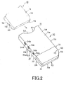
FIG. 2 is a perspective view showing, from the upper side, adapter device in which IC card is loaded. -
FIG. 3 is a perspective view showing, from the lower side, adapter device in which IC card is loaded. -
FIG. 4 is a perspective view showing, from the upper side, small-sized IC card loaded into the adapter device. -
FIG. 5 is a perspective view showing, from the lower side, small-sized IC card loaded into the adapter device. -
FIG. 6 is a perspective plan view for explaining the internal structure of the adapter device. -
FIG. 7 is a plan view for explaining cut portions provided in a manner opposite to each other at the casing rear surface side of the adapter device. - An adapter device for IC card according to the present invention will be explained with reference to the attached drawings.
- As shown in
FIG. 1 , theadapter device 30 according to the present invention is loaded at a loading portion within a host equipment 1 through aninsertion opening 2 provided at the host equipment 1 in the state where there is loaded anIC card 10 in which there is included semiconductor memory used as external memory unit for host equipment 1 such as recording and/or reproducing apparatus for audio data, personal computer, digital still camera and/or digital video camera, etc. Theadapter device 30 is formed so as to have substantially the same size as the existing IC card, and is adapted for permittingIC card 10 smaller than IC card conventionally used to be loaded at host equipment 1 having loading portion corresponding to IC card conventionally used. As shown inFIGS. 2 and3 , theadapter device 30 includes acasing 31 constituting the device body, wherein theIC card 10 is loaded into thecasing 31. - Here, the
IC card 10 to be loaded into thecasing 31 will be explained. ThisIC card 10 is common to the existing IC card in the electric specification, and is different from the latter in the physical specification. In concrete terms, theIC card 10 is miniaturized so that its long side is caused to be shorter than long side of the existing IC card. - The
IC card 10 comprises, as shown inFIGS. 4 and 5 , a substantially rectangular plate-shaped card body 11 obtained by molding synthetic resin material. As shown inFIGS. 4 and 5 , within thecard body 11, there are included semiconductor memory elements such as flash memory, etc. having large memory capacity of 4 MB (mega bytes) or more, e.g., 4 MB, 16 MB, 32 MB, 64 MB, 128 MB, 256 MB or 1 GB, control circuit elements in which control circuit portions for controlling write operation of data such as audio data, etc. with respect to the semiconductor memory elements, or read-out operation of data such as audio data, etc. stored in the semiconductor memory elements, and plural semiconductor integrated circuit elements such as copyright protection circuit elements, etc. in the state where they are mounted on a printed wiring board. - The
card body 11 in which plural semiconductor elements are included as stated above and the printed wiring board on which these semiconductor elements are mounted is included is formed so as to have mechanical strength to such a degree that it is not bent by ordinary external force applied at the time of use, etc. thus to realize protection of included semiconductor elements such as semiconductor memory elements, etc. and the printed wiring board on which these semiconductor elements are mounted. In concrete terms, thecard body 11 is formed by molded body of synthetic resin. - The
IC card 10 is common to the IC card of the standard use already used in the electrical specification, but is different from the latter in the physical specification. In concrete terms, theIC card 10 is adapted so that the outside configuration is miniaturized to more degree as compared to the standard IC card. Namely, as shown inFIG. 4 , thecard body 11 is formed as rectangular shape in which length W of the short side is caused to be substantially 20 mm, length L of the long side is caused to be substantially 31 mm, and the thickness T is caused to be substantially 1.6 mm. - It is to be noted that the IC card of the standard size is similar to the above-described
IC card 10 in the fundamental specification, but is different from the latter only in the size thereof. The IC card of the standard size is formed as rectangular shape in which length W of the short side is caused to be substantially 21.45 mm, length L of the long side is caused to be substantially 50 mm, and thickness T is caused to be substantially 2.8 mm. - At the side of one short side of the
card body 11, as shown inFIG. 5 , there is formed aterminal portion 12 in a manner extending fromfront surface 11a serving as insertion end into the host equipment towardbottom surface 11b. At theterminal portion 12, there are provided plural engagement recessedportions 14 partitioned bypartition walls 13 in correspondence with the number ofelectrodes 15. The respective engagement recessedportions 14 are opened in a manner extending from thefront surface 11 a of thecard body 11 toward thebottom surface 11b thereof so that a group of terminals provided at the loading portion side of the host equipment can be engaged thereinto. Theplural electrodes 15 are provided in the state where they are respectively positioned at the bottom surfaces of the respective engagement recessedportions 14, and are separated from each other by thepartition walls 13. Since pluralrespective electrodes 15 are respectively provided at the bottom surfaces of the engagement recessedportions 14 partitioned so that they are smaller than size of finger of the human being bypartition walls 13, finger and/or large foreign material are prevented from directly being coming into contact with theIC card 10 at the time of handling thereof. Thus, theIC card 10 is securely protected from stain and/or damage, etc. - At the
IC card 10, there are provided tenelectrodes 15 constituting theterminal portion 12. Transmission/reception of data between theIC card 10 and the host equipment to which theIC card 10 is loaded is performed by serial interface through theelectrodes 15 provided at theterminal portion 12. In concrete terms, atleast electrodes 15 are used as at least input termonal for serial protocol bus state signal BS, input terminal for serial protocol data signal SDIO, input terminal for serial clock SCLK, and power supply voltage VCC terminal. It is a matter of course that transmission/reception of data to and from the host equipment may be performed by parallel interface. - At the
front surface 11 a of thecard body 11 and the opening end of thepartition walls 13, there are formed, as shown inFIG. 5 ,inclination surface portions 16 in a manner extending from the middle portion in the thickness direction of thefront surface 11 a of thecard body 11 toward thebottom surface 11b thereof. Theinclination surface portion 16 functions as an insertion guide portion when theIC card 10 is inserted into the insertion/withdrawal portion 2 of the host equipment. Moreover, at thecard body 11, there are providedinclination surface portions 17 in a manner extending from the bottom surfaces of respective engagement recessedportions 14 toward thebottom surface 11b of thecard body 11. When theIC card 10 is loaded at the loading portion of the host equipment, theinclination surface portions 17 permit foreign material such as dust, etc. attached to theelectrodes 15 to be swept out to the external of the engagement recessedportions 14 by the group of terminals of the loading portion side. - At one corner portion of the
front surface 11a side whereterminal portion 12 is formed of thecard body 11, there is provided, as shown inFIGS. 4 and 5 , achamfering portion 18 for permitting user to easily discriminate insertion direction into the host equipment or theadapter device 30. At thebottom surface 11b of the side where thechamfering portion 18 is formed of thecard body 11, there is provided ahollow portion 19 which opens theside surface 11c side of the side where thefront surface 11 a and thechamfering portion 18 are provided and which is formed in a manner lower by one step with respect to thebottom surface 11b of thecard body 11. At thehollow portion 19, there is provided a projectedportion 20 which is continuous to theside surface 11c of the side where thechamfering portion 18 is provided and which has a summit portion of substantially the same height as thebottom surface 11b. As the result of the fact that the projectedportion 20 is provided at thehollow portion 19, an erroneous insertion preventing recessedportion 21 with respect to the insertion/withdrawal portion 2 into or from the host equipment is constituted at the inside thereof. When theIC card 10 is inserted into the insertion/withdrawal opening 2 in a normal state, erroneous insertion preventing projection provided at the loading portion of the host equipment is engaged with the erroneous insertion preventing recessedportion 21 to permit loading of theIC card 10. - When the
IC card 10 fails to be inserted into the host equipment from the insertion/withdrawal opening 2 in a normal state, as the result of the fact that the erroneous insertion preventing projection of the host equipment 1 comes into contact with thefront surface 11a of thecard body 11 in which thechamfering portion 18, thehollow portion 19 and/or the erroneous insertion preventing recessedportion 21 are provided, it is limited that theplural electrodes 15 and a group of terminals of the host equipment side are engaged with engagement recessedportions 14 partitioned bypartition walls 13. Thus, therespective electrodes 15 are prevented from coming into contact with a group of terminals of the host equipment side to realize protection of theseelectrodes 15 and semiconductor integrated circuit elements included within thecard body 11. - At the
bottom surface 11b of the side where thechamfering portion 18 is formed of thecard body 11, as shown inFIG. 5 , there is provided, in the vicinity ofhollow portion 19, a slip-off or falling-off preventing recessedportion 22 for preventing slip-off from the loading portion of theIC card 10 when theIC card 10 is loaded with respect to the loading portion of the host equipment. The slip-off preventing recessedportion 22 is provided in a manner to open oneside surface 11c which is in parallel to insertion direction into the host equipment of theIC card 10 and thebottom surface 11b. The slip-off preventing piece of the loading portion side of the host equipment is engaged with the slip-off preventing recessedportion 22 only when theIC card 10 is inserted into the insertion/withdrawal portion 2 with respect to the host equipment in a normal state. It is to be noted that, as the result of the fact that theprojection 20 constituting the above-described erroneous insertion preventing recessedportion 21 is provided in a manner continuous to oneside surface 11c of thecard body 11 and the front end portion of thefront surface 11a side is formed so as to take substantially arc shape, when theIC card 10 is loaded with respect to the loading portion of the host equipment, the slip-off prevention piece comprised of the elastic piece, etc. which is caused to undergo elastic displacement in the short side direction of theIC card 10 to be inserted smoothly rides on theside surface 11c so that it is engaged with the slip-off preventing recessedportion 22. - At the
bottom surface 11b of the side where thechamfering portion 18 is formed of thecard body 11, there is provided, at thefront surface 11a side of thecard body 11, a recessedportion 23 for eject with which eject mechanism for ejectingIC card 10 provided at the loading portion side of the host equipment from the loading portion is engaged. The eject recessedportion 23 is provided in a manner to open the portion extending from theother side surface 11d in parallel to the insertion direction into the host equipment of theIC card 10 to thebottom surface 11b, and the eject mechanism of the loading portion side is engaged with theeject recess portion 23 only when theIC card 10 is inserted into the insertion/withdrawal opening 2 with respect to the host equipment in a normal state. - At the
bottom surface 11b side of thecard body 11, there is provided an erroneousrecording prevention switch 24 positioned in the vicinity of theterminal portion 12 and serving to prevent that data is erroneously recorded into the semiconductor memory. The erroneousrecording prevention switch 24 can be moved in the same direction as insertion/withdrawal direction with respect to the host equipment of theIC card 10, and is connected to operation element provided on the printed wiring board within thecard body 11. The erroneousrecording preventing switch 24 is adapted so that when it is sled in one direction, recording of data can be permitted, while when it is slid in the other direction, overwrite operation of new data is inhibited. - Further, the
IC card 10 is provided, at therear surface 11e of thecard body 11, with a discrimination recessedportion 25 for discriminating between audio IC card having copyright management function with a view to preserving audio data and general purpose IC card with a view to preserving other data such as processing data processed at the computer, etc. The discrimination recessedportion 25 is provided only at the audio IC card, and is not provided at the general purpose IC card. Accordingly, theIC card 10 provided with the discrimination recessedportion 25 is used for the purpose of preservation of audio data. - In concrete terms, the discrimination recessed
portion 25 is provided at the position shifted from the center of the width direction perpendicular to the insertion direction into the host equipment in which the IC card is loaded of thecard body 11 toward oneside surface 11c side where thechamfering portion 18 is provided of thecard body 11. Other recessed portions, i.e., engagement recessedportion 14,hollow portion 19, erroneous insertion preventing recessedportion 21 slip-off prevention recessedportion 22 and eject recessedportion 23 are adapted so that thebottom surface 11b side of thecard body 11 is opened and thetop face 11f side of thecard body 11 is closed, whereas the discrimination recessedportion 25 is continuous, i.e., is penetrated extending from thetop face 11f of thecard body 11 toward thebottom face 11b and its side surface is formed by curve so that smooth feel is provided. - Further, at the
bottom surface 11b of thecard body 11, there is provided amemorandum area 26. Within thememorandum area 26, indication indicating machine kind name of theIC card 10 and/or recording contents recorded with respect to theIC card 10, etc. are implemented by printing or marking, etc., and recording content is directly described as memorandum by using pen by user. It is a matter of course that thememorandum area 26 may be provided at thetop face 11f side, and such memorandum areas may be provided on both thebottom face 11b and thetop face 11f. Further, label may be stuck into thememorandum area 26. - The
IC card 10 which has been small-sized while complying with the fundamental configuration of the standard IC card as described above cannot be loaded at host equipment 1 such as recording and/or reproducing apparatus for audio data, personal computer, digital still camera or digital video camera, etc. which can exclusively load only IC card having the standard dimensions. Theadapter device 30 according to the present invention permits the small-sized IC card 10 to be loaded with respect to the host equipment 1 which can exclusively load only IC card having standard dimensions. Namely, theadapter device 30 serves to permit the small-sized IC card 10 to be loaded with respect to the host equipment 1 for IC card of the standard use while maintaining compatibility with the IC card of the standard specification. Theadapter device 30 is formed so as to take substantially the same dimensions as those of the IC card constituted by the above-described standard specification, and permits the small-sized IC card 10 to be loaded with respect to the host equipment 1 having loading portion corresponding to the IC card of the standard specification. - As shown in
FIGS. 2 and3 , theadapter device 30 includes acasing 31 constituting the device body. TheIC card 10 is loaded within thecasing 31. - The
adapter device 30 which allows the small-sized IC card to be substantially equal to the IC card of the standard size in the outer appearance shape comprises, as shown inFIGS. 2 and3 , casing 31 having substantially the same size as the standard IC card as described above and formed so as to take substantially rectangular shape. Thecasing 31 includes alower case 32 formed so as to take substantially the same size as that of the standard IC card, anupper case 33 attached to thelower case 32 and attached to thefront surface 31a of the insertion side into the host equipment 1 or theadapter device 30 of thelower case 32, and acover 34 attached to thelower case 32 together with theupper case 33 and serving to hold theIC card 10. Thecasing 31 constitutes, therewithin, aloading portion 35 in which theIC card 10 is loaded. - The
lower case 32 is formed by injection-molding synthetic resin so as to have substantially the same size as that of the conventional IC card, and arelay board 36 comprised of printed wiring board having rigidity is disposed, as shown inFIG. 6 , at thefront surface 31 a side of thecasing 31. Therelay board 36 is formed so as to take rectangular shape, wherein a plurality offirst contacts 37 with which a group of terminals provided at the loading portion of the host equipment 1 are caused to be in contact are provided at one side of the long side, i.e., at thefront surface 31a side of thecasing 31 in correspondence with the number ofelectrodes 15 of theIC card 10, in concrete terms, tenfirst terminals 37 are provided in line. Moreover, at the other portion of the long side of therelay board 36, pluralsecond contacts 38 to which a terminal plate 42 for realizing electrical connection to theelectrodes 15 of theIC card 10 is electrically connected by soldering, etc. are provided in correspondence with the number of thefirst contacts 37. Atsuch relay board 36, recessedportions portions positioning projections lower case 32, therelay board 36 is attached in a manner extending in the short side direction of thelower case 32 in the case where it has been caused to undergo positioning at thelower case 32. - At the
lower case 32, there is attached a terminal plate 42 for electrically connecting theterminal portion 12 of theIC card 10 loaded at theloading portion 35 and therelay board 36 in a manner adjacent to therelay board 36. The terminal plate 42 is constituted by fixing conductive plural terminal members by insulating resin member, and the entirety thereof is formed so as to take substantially rectangular shape. Plural terminal members fixed in the state electrically insulated by resin member exist by the number of first andsecond contacts second contact 38 of therelay base 36 and the other end portion serves as aconnection terminal 44 which is caused to be in pressure contact with theelectrodes 15 constituting theterminal portion 12 of theIC card 10. In concrete terms, the terminal 43 is positioned at therelay board 36 side, and is electrically connected to thesecond contact 38 of therelay board 36 by soldering, etc. Moreover, theconnection terminal 44 of theloading portion 35 side is constituted by elastic piece bent so as to take substantially L-shape. Theconnection terminal 44 is extended toward theloading portion 35 side, whereby it comes into pressure contact with theelectrode 15 of theIC card 10 when theIC card 10 is loaded at theloading portion 35. As a result, theconnection terminal 44 is electrically connected to theelectrode 15 of theIC card 10, and serves to hold theIC card 10 at theloading portion 35. - In such terminal plate 42, positioning holes 45, 45 are provided at one short side, and a positioning recessed
portion 46 is formed at the other short side. At therelay board 36, as shown inFIG. 6 ,positioning projections lower case 32 are inserted into positioning holes 45, 45, and apositioning projection 49 provided at thelower case 32 is engaged with the positioning recessedportion 46. Further, by implementing ultrasonic soldering, etc. topositioning projections positioning projection 49, therelay board 36 is attached in a manner extending in the short side direction of thelower case 32 in the state where it has been caused to undergo positioning at thelower case 32. - Moreover, at the
lower case 32, there is provided aloading portion 35 in which theIC card 10 is loaded in a manner adjacent to the terminal plate 42. At theloading portion 35, there is provided an erroneousinsertion preventing projection 51 for preventing erroneous insertion of theIC card 10. The erroneousinsertion preventing projection 51 is formed so as to take substantially L-shape, wherein the long side is extended in the insertion direction of theIC card 10. When theIC card 10 is inserted in a normal state, the erroneousinsertion preventing projection 51 is engaged with the erroneous insertion preventing recessedportion 21 provided at thefront surface 11a of theIC card 10. Moreover, when theIC card 10 is inserted in the abnormal state, e.g., in the back state, the erroneousinsertion preventing projection 51 collides against thefront surface 11a of theIC card 10 so that it is not engaged with the erroneous insertion preventing recessedportion 21. Thus, the erroneousinsertion preventing projection 51 serves to prevent theIC card 10 from being loaded with respect to theloading portion 35. - The
relay board 36 and the terminal plate 42 which have been described above are attached to predetermined positions of the front portion of thelower case 32 as described above. Thereafter, theupper case 33 is attached to the front portion of thelower case 32 by ultrasonic welding, etc. Namely, when theupper case 33 is attached to thelower surface 32, it constitutes a parts accommodating portion which accommodates therelay board 36 and/or the terminal plate 42. Thecover 34 is attached to thelower case 32 in such a manner continuous to theupper case 33. When thecover 34 is attached to thelower case 32, it constitutes, along with thelower case 32,loading portion 35 in which theIC card 10 is loaded. As the result of the fact that thecover 34 is attached to thelower case 32, an insertion/withdrawal opening 52 for inserting theIC card 10 into theloading portion 35 is constituted at the rear surface side opposite to thefront surface 31 a of thecasing 31. - At the
front surface 31 a side of thecasing 31 constituted as the result of the fact that theupper case 33 and thecover 34 are attached to thelower case 32, as shown inFIGS. 2 and3 , there is provided aterminal portion 53 required for allowing theadapter device 30 to perform transmission/reception of data to and from the host equipment 1. Theterminal portion 53 includesplural partition walls 54 which partition thefirst contacts 37 provided on the above-describedrelay board 36, and thesepartition walls 54 constitute plural engagement recessedportions 55 with which a group of terminals provided at the loading portion side of the host equipment 1 are engaged. At these engagement recessedportions 55, thefront surface 31a side and thebottom face 31b side of thecasing 31 are opened so that a group of terminals provided at the loading portion side of the host equipment 1 can be engaged with these engagement recessedportions 55. Thefirst contacts 37 are provided at the bottom surfaces of respective engagement recessedportions 55, and are separated by thepartition walls 54. As the result of the fact that thefirst contact 37 is provided at the bottom surface of the engagement recessedportion 55, it is prevented by the engagement recessedportion 55 that finger, etc. directly comes into contact with thefirst contact 37. Thus, thefirst contacts 37 are protected. - In this example, respective
first contacts 37 constituting theterminal portion 53 are connected in series withrespective connection terminals 44 through therelay board 36 and the terminal plate 42 without providing intermediate circuits such as data converting circuit and/or amplifier circuit, etc. in the state where the electric circuit configuration has been simplified. It is a matter of course that intermediate circuits such as data converting circuit and/or amplifier circuit, etc. may be provided between thefirst contacts 37 and theconnection terminal 44. - Moreover, at the
front surface 31 a of thecasing 31 and the opening end of thepartition walls 54, as shown inFIG. 3 , there are providedinclination surface portions 61 in a manner extending from the middle portion of the thickness direction of thefront surface 31a of thecasing 31 toward thebottom surface 31b. Theinclination surface portion 61 functions as an insertion guide portion in inserting theadapter device 30 into the insertion/withdrawal opening 2 of the host equipment 1. Further, at thecasing 31, there are providedinclination surface portions 62 in a manner extending from the bottom surfaces of respective engagement recessedportions 55 toward thebottom surface 31b of thecasing 31. When theadapter device 30 is loaded with respect to the loading portion of the host equipment 1, theinclination surface portions 62 are adapted to have ability to sweep out foreign material such as dust, etc. attached to thefirst contact 37 toward the external portion of the engagement recessedportion 55 by a group of terminals of the loading portion side of the host equipment 1. - Further, at one corner portion of the
front surface 31a side whereterminal portions 53 are formed of thecasing 31, there is provided achamfering portion 56 in order that user can easily discriminate insertion direction of the host equipment 1 of theadapter device 30. Atbottom surface 31b of the side where thechamfering portion 56 is formed of thecasing 31, there is provided ahollow portion 57 which opens theside surface 31c side of the side where thefront surface 31a and thechamfering portion 56 are provided, and which is lower by one step with respect to thebottom surface 31b of thecasing 31. Thehollow portion 57 functions as an erroneous insertion preventing groove with respect to the host equipment 1 of theadapter device 30. Only when theadapter device 30 is inserted into the loading portion of the host equipment 1 in a normal state, an erroneous insertion preventing projection provided at the loading portion of the host equipment 1 side is engaged with thehollow portion 57. Namely, when theadapter device 30 is inserted into the loading portion of the host equipment 1 in the abnormal state, e.g., in back side state, the erroneous insertion preventing groove constituted by thehollow portion 57 collides against thefront surface 31a of thecasing 31 so that theadapter device 30 is not loaded into the loading portion of the host equipment 1. Thus, a group of terminals provided at the loading portions of the host equipment 1 are prevented from being engaged with the engagement recessedportion 55 so that thefirst contact 37 is not damaged. - Further, at the
bottom surface 31b of the side where thechamfering portion 56 is formed of thecasing 31, there is provided, in the vicinity of thehollow portion 57, a slip-off preventing recessedportion 58 for preventing theIC card 10 from being slipped off when theIC card 10 is loaded at the loading portion of the host equipment 1. The slip-off preventing recessedportion 58 is provided in a manner to open oneside surface 31c in parallel to insertion direction into the host equipment of theIC card 10 and thebottom surface 31b so that the slip-off prevention piece of the loading portion side of the host equipment 1 can be engaged with the slip-off preventing recessedportion 58 only when theIC card 10 is inserted into the insertion opening of the host equipment in a normal state. - Further, at the
bottom surface 31 b of theside surface 31d side of the side opposite to theside surface 31c of thecasing 31, there is provided, at the middle portion thereof, a recessedportion 59 for eject with which an eject mechanism for ejecting, from the loading portion, theIC card 10 provided at the loading portion side of the host equipment is engaged. The eject recessedportion 59 is provided in such a manner that theother side surface 31d in parallel to insertion direction into the host equipment of theIC card 10 and thebottom surface 31b are opened. Only when theIC card 10 is inserted into the insertion opening of the host equipment 1 in a normal state, the eject mechanism of the loading portion side of the host equipment 1 can be engaged with the eject recessedportion 59. - Further, as shown in
FIG. 2 , at thetop face 31e of thecasing 31, a first insertiondirection indication portion 63 indicating insertion direction into the host equipment 1 of theadapter device 30 is provided by sign such as triangle, etc. The first insertiondirection indication portion 63 is formed by printing or marking, etc. in the vicinity of thechamfering portion 56 of theupper case 33. Thetop face 31e of thecasing 31 is the area noticed for user to the greatest degree. In this example, at theadapter device 30, the configuration functionally required which is provided on thetop face 31e of thecasing 31 is caused to be only first insertiondirection indication portion 63, thereby making it possible to freely implement design onto thetop face 31e of thecasing 31. In addition, at theadapter device 30, the configurations functionally required are provided to more degree at thebottom surface 31b in dependency upon the degree that these configurations are not provided on thetop face 31e of thecasing 31. - At the
bottom surface 31b of thecasing 31, as shown inFIG. 3 , there are provided a second insertiondirection indication portion 64 indicating insertion direction into the host equipment 1 of theadapter device 30 and insertion direction into theadapter device 30 of theIC card 10, and an insertionattitude indication portion 65 indicating insertion attitude into theadapter device 30 of theIC card 10. The second insertiondirection indication portion 64 and the insertionattitude indication portion 65 are formed by printing or marking, etc. At the second insertiondirection indication portion 64, e.g., arrow indicating insertion direction into the host equipment 1 is illustrated. At the insertionattitude indication portion 65, model view of theIC card 10 is illustrated. TheIC card 10 is inserted into theadapter device 30 with thefront surface 11a being as insertion end in such a manner that thebottom surface 31b of thecasing 31 and thebottom surface 11b of theIC card 10 are opposed to each other. In view of the above, the insertionattitude indication portion 65 is caused to be of the configuration so that face and back and the insertion end when theIC card 10 is inserted into theadapter device 30 can be visually confirmed by user. Namely, when user looks at thebottom surface 31b with thebottom surface 31b of thecasing 31 being positioned at this side, user is required to insert theIC card 10 into the insertion/withdrawal opening 52 of theadapter device 30 in the state where thebottom surface 11b of theIC card 10 is positioned at this side and thefront surface 11a is caused to be insertion end. In view of the above, at the insertionattitude indication portion 65, model view of thebottom surface 11b in which thefront surface 11a of theIC card 10 is caused to be thefront surface 31a side of thecasing 31 is illustrated. - The
cover 34 which constitutes thetop face 31e of thecasing 31 along with theupper case 33 is formed by material different from that of thelower case 32 or theupper case 33, and is formed by bending steel metal having mechanical strength higher than that of thelower case 32 or theupper case 33 which is molded by, e.g., resin. Thecover 34 is adapted so that both side edges in length direction are formed to be substantially channel-shaped in cross section, and constitutes thetop face 31e of thecasing 31 and is formed in such a manner to cover side walls formed in rising manner at both side edge portions in length direction of the lower case and both side edge portions in length direction of thebottom surface 31b. Thecover 34 is fixed on thelower case 32 as the result of the fact that holdingprojections 34a formed at the side walls of thelower case 32 are held at holdingholes 34b provided in correspondence with holdingprojections 34a. Because steel metal having high mechanical strength is used, thecover 34 serves to enhance holding force of theIC card 10 loaded at theloading portion 35 while realizing thin structure of thetop face 31e of thecasing 31, and can sufficiently protect the loadedIC card 10 from external pressure such as impact, etc. - As shown in
FIG. 7 , an insertion/withdrawal opening 52 of theIC card 10 is formed by the rear surface side of thelower case 32 which constitutes thebottom surface 31b of thecasing 31 and the rear surface side of thecover 34 which constitutes thetop face 31 e of thecasing 31. At the rear surface sides of thetop face 31e and thebottom surface 31 b of thecasing 31, there are formed, in a manner continuous to the insertion/withdrawal opening 52, cutportions top face 11f and thebottom face 11b of theIC card 10 loaded at theloading portion 35 to be exposed. - The
cut portion 67 formed at thetop face 31e of thecasing 31 is formed at the end portion of the rear surface side of thecover 34, and thecut portion 68 formed at thebottom surface 31b of thecasing 31 is formed at the end portion of the rear surface side of thelower case 32. These cutportions top face 11f and thebottom face 11b of the rear surface side of theIC card 10 toward the external. When theIC card 10 is loaded at theloading portion 35, thecut portions top face 11f and thebottom face 11b of the rear surface side of theIC card 10 toward the external so that user grasps thetop face 11f and thebottom face 11b to have ability to easily draw out theIC card 10 from theloading portion 35. - The
cut portion 68 of thebottom surface 31b side of thecasing 31 is formed so that it is greater than thecut portion 67 of thetop surface 31e side. At thebottom surface 31b side of thecasing 31, there is providedmemorandum area 26 of theIC card 10. When theIC card 10 is loaded at theloading portion 35, thecut portion 68 serves to face thememorandum area 26 toward the external so that thememorandum area 26 can be visually recognized in the state where theIC card 10 is loaded at theadapter device 30. Moreover, thecut portion 67 of thetop face 31e side of thecasing 31 and thecut portion 68 of thebottom face 31b side thereof are caused to have shapes different from each other, whereby, at the time of loading of theIC card 10 or at the time of insertion into the host equipment 1 of theadapter device 30, user can confirm face side and back side of theadapter device 30 by feeling. - The
cut portions casing 31 being as reference. Thus, user is permitted to facilitate user to grasp theupper face 11f and thebottom face 11b of the rear surface side of theIC card 10 which have been faced from thecut portions memorandum area 26 of theIC card 10 can be faced fromcut portion 68 of thebottom face 31b side of thecasing 31 toward the external. - In concrete terms, cut
portion 67 formed at theupper face 31e of thecasing 31 and cutportion 68 formed at thebottom face 31b thereof are formed so that the end surfaces take substantially circular arc and cut quantity on the center line P in width direction of thecasing 31 is maximum. It is to be noted that shapes ofcut portions - In this example, the
cover 34 constituting theloading portion 35 is formed by sheet metal. Accordingly, when insertion/withdrawal of the IC card is performed,IC card 10 formed by synthetic resin and cover 34 formed by sheet metal come into contact with each other so that any defect would take place at the surface of theIC card 10. In view of the above, fluorine coating may be implemented, as protective coating, to the insertion/withdrawal opening 52 side of the back side of at least loadingportion 35 side of thecover 34. Moreover, fluorine coating may be implemented also to the surface side constituting the armor of thecover 34 in order to constitute a portion of armor. Further, fluorine coating may be implemented also to the peripheral portion of the insertion/withdrawal opening 52 to have ability to prevent finger, etc. of user from being damaged by burr formed at the end portion of thecover 34, etc. The area where fluorine coating is implemented to the surface of thecover 34 may be provided at least at the rear surface side of thecover 34, i.e., at the peripheral portion of the insertion/withdrawal opening 52, and other areas may be changed as occasion demands in dependency upon the armor. - Then, a method of inserting the
IC card 10 into theadapter device 30 will be explained. As shown inFIGS. 2 and6 , theIC card 10 is inserted into the insertion/withdrawal opening 52 of theadapter device 30 in the state where thetop face 11f is caused to betop face 31e side of thecasing 31 with thefront surface 11a whereterminal portions 12 are provided of thecard body 11 being as insertion end. Further, when theIC card 10 is inserted from the insertion/withdrawal opening 52 of theadapter device 30 in a normal state, erroneousinsertion preventing projection 51 is engaged with erroneous insertion preventing recessedportion 21 at theIC card 10. Theconnection terminal 44 faced to theloading portion 35 admits into engagement recessedportion 14 which constitutes theterminal portion 12 of theIC card 10 so that it comes into pressure contact with thefirst contact 37. Thus, there results the state where theadapter device 30 and theIC card 10 are electrically connected. Namely, theelectrode 15 of theIC card 10 and thefirst contact 37 of theadapter device 30 are electrically connected through therelay board 36 and the terminal plate 42. In the state where theIC card 10 is normally inserted into theadapter device 30, theadapter device 30 is placed in the state where the entirety of theIC card 10 is accommodated at theloading portion 35. TheIC card 10 has the same dimensions as those of existing IC cards, resulting in the state where loading into the loading portion of the host equipment 1 can be made. - When the
IC card 10 is inserted into theadapter device 30, user visually recognizes the secondinsertion indication portion 64 and the insertionattitude indication portion 65 which are provided at thebottom surface 31b of thecasing 31 to thereby to confirm the insertion direction or the insertion attitude of theIC card 10 thereafter to have ability to perform insertion operation into theadapter device 30 of theIC card 10. Accordingly, it is prevented that theconnection terminal 44 provided at theloading portion 35 is stained by erroneous insertion of theIC card 10. Moreover, the face side and the back side of theadapter device 30 can be confirmed by visually recognizing or feeling shapes ofcut portion casing 31. Thus, user confirms the face side and the back side of theadapter device 30 thereafter to perform insertion operation of theIC card 10, thereby making it possible to prevent erroneous insertion of theIC card 10. - The
memorandum area 26 provided at the rear surface side of thebottom surface 11b of theIC card 10 is faced to the outside from thecut portion 68 in the state where theIC card 10 is loaded into theadapter device 30. Thus, user can confirm the content described in thememorandum area 26 by visual recognition. - It is to be noted that when the
IC card 10 is inserted into theadapter device 30 in the back state where thebottom face 11b is upwardly positioned or in the state in opposite direction in which therear surface 11e is caused to be the insertion side, the erroneousinsertion preventing projection 51 provided at theloading portion 35 collides with thefront surface 11a or therear surface 11e so that theIC card 10 is not loaded into theloading portion 35. Thus, theIC card 10 is placed in the state where therear surface 11e side is projected from the insertion/withdrawal opening 52. As a result, user can immediately recognize that insertion direction of the IC card is erroneous. - The
IC card 10 loaded at theloading portion 35 of theadapter device 30 can be easily drawn out from theloading portion 35 of theadapter device 30 in the state where thetop face 11f and thebottom face 11b of the rear surface side of theIC card 10 exposed to the external fromcut portions - Then, explanation will be given with reference to
FIG. 1 in connection with a method of inserting the IC card into the host equipment 1 of theadapter device 30 in which theIC card 10 is loaded at theloading portion 35. Theadapter device 30 is inserted into the insertion/withdrawal opening 2 of the host equipment 1 in the state where thetop face 31e is positioned at the upper side with thefront surface 31a where theterminal portion 53 is provided of thecasing 31 being as insertion end. When theadapter device 30 is inserted in a normal state from the insertion/withdrawal opening 52, erroneous insertion preventing projection provided at the loading portion of the of the host equipment 1 is engaged with the erroneous insertion preventing groove constituted by thehollow portion 57 at theadapter device 30. Moreover, slip-off prevention piece comprised of elastic piece provided at the loading portion of the host equipment 1 is engaged with slip-off prevention recessedportion 58. Further, as the result of the fact that a group of terminals of the loading portion of the host equipment 1 admits from engagement recessedportion 55 to thefirst contact 37 which constitutes theterminal portion 53, the group of terminals is placed in pressure contact state. Thus, there results the state where transmission/reception of data to and from theIC card 10 electrically connected to theadapter device 30 can be made. - As stated above, since the
chamfering portion 56 is provided at thefront surface 31 a side of thecasing 31 serving as insertion end into the host equipment 1 when user inserts the host equipment 1 into theadapter device 30, it is possible to easily discriminate insertion direction. Moreover, at theadapter device 30, since any recessed portion is not provided at theupper surface 31e, and engagement recessedportion 55,hollow portion 57, slip-off prevention recessedportion 58 and eject recessedportion 59 are provided at thebottom surface 31b side, difference between shape of thetop face 31e and that of thebottom surface 31b is confirmed. In addition, difference between shape ofcut portion 67 and that ofcut portion 68 which are provided at the rear surface portion of thecasing 31, thereby making it possible to confirm face side and back side at the time of insertion into the host equipment 1. Further, user visually recognizes first insertiondirection indication portion 63 provided on theupper surface 31e of thecasing 31, thereby making it possible to confirm insertion direction into theinsertion opening 2 of the host equipment 1 of theadapter device 30. - In this example, when the
adapter device 30 is inserted into the host equipment 1 in the back state where thebottom surface 31b is positioned in upper direction, or in the reverse state where the rear surface is caused to be the insertion side, the erroneous insertion preventing projection provided at the loading portion of the host equipment 1 collides against thefront surface 31a or the rear surface so that theadapter device 30 is not loaded at the loading portion. Thus, user can immediately recognize that insertion direction of theIC card 10 is erroneous. - In this case, the
adapter device 30 loaded at the host equipment 1 is ejected from the insertion/withdrawal opening 2 toward the external by eject mechanism engaged with the eject recessedportion 59 provided at thecasing 31. - In the
adapter device 30 as described above, the insertion direction of theIC card 10 is the same as the insertion direction into the host equipment 1 of theIC card 10, the insertion direction into the host equipment 1 of the existing IC card, and the insertion direction into the host equipment 1 of theadapter device 30. Thus, user can easily recognize insertion direction into theadapter device 30 of theIC card 10. - Moreover, at the
adapter device 30, since erroneousinsertion preventing projection 51 to be engaged with the erroneous insertion preventing recessedportion 21 of theIC card 10 is provided at theloading portion 35, it is possible to prevent erroneous insertion into theadapter device 30 of theIC card 10. Namely, when theIC card 10 is erroneously inserted into theadapter device 30, the outer surface side of theIC card 10 is projected from the insertion/withdrawal opening 52. From this fact, user can easily recognize that insertion of theIC card 10 is erroneous insertion. - At the
adapter device 30, since thecut portions casing 31 are formed in the state where their shapes are different from each other, it is possible to confirm face side and back side. After confirmation of the face side and the back side, insertion direction and/or insertion attitude of theIC card 10 can be further confirmed by the second insertiondirection indication portion 64 or the insertionattitude indication portion 65 provided at thebottom surface 31b of thecasing 31. As described above, at theadapter device 30, since user can perform operation confirmation of theIC card 10 by various means before insertion operation of theIC card 10, it is possible to prevent, in advance, erroneous insertion of theIC card 10. - Moreover, when the
IC card 10 is loaded into theadapter device 30, thememorandum area 26 provided at thebottom surface 11b of theIC card 10 is faced toward the external fromcut portion 68 provided at thebottom surface 31b side of thecasing 31. Thus, user can confirm description content of thememorandum area 26 even in the state where theIC card 10 is loaded at theadapter device 30. - At the time of loading of the
IC card 10, at theadapter device 30, the rear surface side of theIC card 10 is faced toward the external. Thus, user easily grasps, such as picks up by finger, etc. thetop face 31e and thebottom face 31 b of theIC card 10 faced toward the external from thecut portions IC card 10 attached to theadapter device 30. - Further, at the
adapter device 30, with respect to the display portions functionally required, the first insertiondirection indicating portion 53 is only provided at thetop face 31e of thecasing 31, and the remaining portions are provided at thebottom surface 31b side. Accordingly, it is possible to freely perform design of the top face 3 1 e which is the plane surface noticed for user to the greatest degree. - The IC card 1 loaded to the previously explained
adapter device 30 may be IC card with image pick-up device such as CCD (Charge-Coupled Devices), etc., IC card with GPS (Global Positioning System), and/or IC card for wireless communication interface such as Bluetooth, etc. in addition to the IC card for memory, and its function is not particularly limited. - It is to be noted that while the invention has been described in accordance with preferred embodiments thereof illustrated in the accompanying drawings and described in the above description in detail, it should be understood by those ordinarily skilled in the art that the invention is not limited to embodiments, but various modifications, alternative constructions or equivalents can be implemented without departing from the scope of the present invention as set forth by appended claims.
- As described above, in accordance with the adapter device for electronic equipment (e.g., IC card) according to the present invention, cut portions are provided at surfaces opposite to each other of the device body in a manner opposite to each other. Accordingly, user can take out electronic equipment loaded at the loading portion, e.g., in a manner to pick up upper and lower surfaces of the rear surface side of the electronic equipment exposed from, e.g., cut portions, thus making it possible to realize improvement in operability.
Claims (3)
- An adapter device (3) for receiving electronic equipment (10) such that said electronic equipment does not substantially project out of an insertion/withdrawal opening (52) comprising:a device body (31) for loading with respect to a unit (1) in which the adapter device (3) is to be loaded;a loading portion (35) provided in the device body (31), and adapted to receive said electronic equipment (10) in which electronic equipment at least semiconductor integrated circuit elements are included, the electronic equipment (10) being provided with a first terminal portion (12);a second terminal portion (53) provided on a bottom surface and at one end of the device body said one end at one end serving as insertion end into the unit (1) (31), and adapted for performing transmission/reception of data to and from the unit (1);an insertion/withdrawal opening (52) provided, in a manner continuous to the loading portion (35), at the other end opposite to the one end of the device body;a connecting portion (42) provided at the loading portion (35), and electrically connected to the second terminal portion (53) and connected to the first terminal portion (12) of the electronic equipment (10); andcut portions (67, 68) respectively provided at surfaces opposite to each other on either side of the device body at the other end of the device body having the insertion/withdrawal opening;wherein the cut portions provided at the surfaces opposite to each other are formed so that they are opposite to each other and their dimensions are different from each other, a larger cut portion extending further towards said one end and thereby being significantly larger than a smaller cut portion such that they feel different to a user inserting the electronic equipment (10), into said adapter device; and
wherein the cut portions are linearly symmetrical about and are formed at a center line running from said one end to said other end; and
wherein the cut portion on the bottom surface is greater than the cut portion on a top surface opposite said bottom surface. - The adapter device for electronic equipment as set forth in claim 1,
wherein the second terminal portion and the connecting portion are electrically connected through a relay board disposed on the device body. - The adapter device for electronic equipment as set forth in claim 1,
wherein the loading portion is provided with an erroneous insertion preventing projection (51) engaged with an erroneous insertion preventing recessed portion (21) provided at one end side of the electronic equipment when the electronic equipment is loaded in a normal state.
Applications Claiming Priority (3)
| Application Number | Priority Date | Filing Date | Title |
|---|---|---|---|
| JP2003032829 | 2003-02-10 | ||
| JP2003032829A JP4019965B2 (en) | 2003-02-10 | 2003-02-10 | IC card adapter device |
| PCT/JP2004/000036 WO2004070889A1 (en) | 2003-02-10 | 2004-01-07 | Adaptor device for electronic device |
Publications (3)
| Publication Number | Publication Date |
|---|---|
| EP1594191A1 EP1594191A1 (en) | 2005-11-09 |
| EP1594191A4 EP1594191A4 (en) | 2006-06-14 |
| EP1594191B1 true EP1594191B1 (en) | 2009-08-12 |
Family
ID=32844351
Family Applications (1)
| Application Number | Title | Priority Date | Filing Date |
|---|---|---|---|
| EP04700530A Expired - Fee Related EP1594191B1 (en) | 2003-02-10 | 2004-01-07 | Adaptor device for electronic device |
Country Status (10)
| Country | Link |
|---|---|
| US (1) | US7118421B2 (en) |
| EP (1) | EP1594191B1 (en) |
| JP (1) | JP4019965B2 (en) |
| KR (1) | KR101016554B1 (en) |
| CN (1) | CN100448108C (en) |
| AU (1) | AU2004209776B2 (en) |
| BR (1) | BRPI0403933A (en) |
| DE (1) | DE602004022512D1 (en) |
| TW (1) | TWI276000B (en) |
| WO (1) | WO2004070889A1 (en) |
Families Citing this family (22)
| Publication number | Priority date | Publication date | Assignee | Title |
|---|---|---|---|---|
| US8397998B1 (en) * | 1999-10-23 | 2013-03-19 | Ultracard, Inc. | Data storage device, apparatus and method for using same |
| JP2006190584A (en) * | 2005-01-07 | 2006-07-20 | Nippon Telegr & Teleph Corp <Ntt> | Transceiver interface conversion adapter |
| JP2007034612A (en) | 2005-07-26 | 2007-02-08 | Sony Corp | Card tray |
| JP4597020B2 (en) | 2005-09-30 | 2010-12-15 | ホシデン株式会社 | Memory card adapter |
| TWM300918U (en) * | 2006-04-12 | 2006-11-11 | Silicon Motion Inc | Memory stick convert device |
| US7249975B1 (en) * | 2006-08-10 | 2007-07-31 | Sun-Light Electronic Technologies Inc. | Micro SD adapter structure |
| TWM324255U (en) * | 2007-02-16 | 2007-12-21 | A Data Technology Co Ltd | Portable storage device with fingerprint identification function |
| US8762640B2 (en) * | 2007-06-27 | 2014-06-24 | Sandisk Il Ltd. | Method for operating a memory interface with SIM functions |
| JP4889686B2 (en) * | 2007-12-28 | 2012-03-07 | モレックス インコーポレイテド | Adapter for card |
| US8491339B2 (en) | 2007-12-28 | 2013-07-23 | Molex Incorporated | Card adapter |
| JP4889687B2 (en) * | 2007-12-28 | 2012-03-07 | モレックス インコーポレイテド | Adapter for card |
| WO2009086530A1 (en) * | 2007-12-28 | 2009-07-09 | Molex Incorporated | Card adapter |
| KR20100030126A (en) * | 2008-09-09 | 2010-03-18 | 삼성전자주식회사 | Memory device and electronic apparatus comprising the same |
| USD642578S1 (en) * | 2009-09-30 | 2011-08-02 | Sony Corporation | Memory card adapter |
| JP5665308B2 (en) * | 2009-12-01 | 2015-02-04 | Necパーソナルコンピュータ株式会社 | Status detection system and relay connector unit |
| JP5523073B2 (en) * | 2009-12-02 | 2014-06-18 | 株式会社バンダイ | Card holder |
| US8550858B2 (en) * | 2010-04-07 | 2013-10-08 | Apple Inc. | Extensible memory card-compatible receptacle and port expansion device |
| JP5655679B2 (en) * | 2011-04-05 | 2015-01-21 | 富士通株式会社 | Card adapter and electronic device |
| US20160294087A1 (en) * | 2013-11-26 | 2016-10-06 | Hewlett Packard Enterprise Development Lp | Electrical connector adapter |
| JP6613130B2 (en) * | 2015-12-22 | 2019-11-27 | モレックス エルエルシー | Card holding member and card connector set |
| TWM542219U (en) * | 2016-12-01 | 2017-05-21 | 勁永國際股份有限公司 | Fingerprint flash drive |
| KR102392767B1 (en) * | 2018-12-26 | 2022-04-28 | 주식회사 엘지에너지솔루션 | Battery Module Having Inner Cover |
Citations (3)
| Publication number | Priority date | Publication date | Assignee | Title |
|---|---|---|---|---|
| WO1999063483A1 (en) * | 1998-05-29 | 1999-12-09 | Smartdiskette Corporation | Smart-card and memory module adapter |
| EP1022645A2 (en) * | 1999-01-21 | 2000-07-26 | Japan Solderless Terminal Mfg. Co., Ltd. | Card connection adaptor |
| DE20215181U1 (en) * | 2002-08-28 | 2003-01-09 | Carry Computer Eng Co Ltd | XD memory card adapter |
Family Cites Families (69)
| Publication number | Priority date | Publication date | Assignee | Title |
|---|---|---|---|---|
| US4908817A (en) * | 1986-11-14 | 1990-03-13 | Opticord, Inc. | Cartridge for optical data discs |
| US5184282A (en) * | 1989-02-27 | 1993-02-02 | Mips Co., Ltd. | IC card adapter |
| JPH06195524A (en) * | 1992-09-14 | 1994-07-15 | Toshiba Corp | Memory card device |
| US6665190B2 (en) * | 1992-09-16 | 2003-12-16 | James E. Clayton | Modular PC card which receives add-in PC card modules |
| US5887145A (en) * | 1993-09-01 | 1999-03-23 | Sandisk Corporation | Removable mother/daughter peripheral card |
| US7137011B1 (en) * | 1993-09-01 | 2006-11-14 | Sandisk Corporation | Removable mother/daughter peripheral card |
| US5773332A (en) * | 1993-11-12 | 1998-06-30 | Xircom, Inc. | Adaptable communications connectors |
| US6773291B1 (en) * | 1993-11-12 | 2004-08-10 | Intel Corporation | Compliant communications connectors |
| US6457647B1 (en) * | 1993-11-16 | 2002-10-01 | Canon Kabushiki Kaisha | Memory card adaptor to facilitate upgrades and the like |
| US6381622B1 (en) * | 1994-12-29 | 2002-04-30 | Via-Cyrix, Inc. | System and method of expediting bit scan instructions |
| JPH09140432A (en) * | 1995-11-21 | 1997-06-03 | Shuichi Shirota | Card holder for automatic ticket examination machine |
| FR2741976B1 (en) * | 1995-11-30 | 1998-01-16 | Gemplus Card Int | REMOVABLE PLUG-IN CARD, FORMING CHIP CARD READER FOR MICROCOMPUTER |
| US5785541A (en) * | 1996-01-31 | 1998-07-28 | Methode Electronics, Inc. | Clockspring tamper prevention and detection seal and method |
| DE29607253U1 (en) * | 1996-04-22 | 1996-07-04 | Stocko Metallwarenfab Henkels | Combi chip card reader |
| JPH1097599A (en) * | 1996-09-24 | 1998-04-14 | Hitachi Ltd | Portable terminal equipment for ic card |
| JPH1125233A (en) | 1997-02-07 | 1999-01-29 | Oki America Inc | Method and device for ic card |
| DE29704984U1 (en) | 1997-03-19 | 1997-05-07 | Stocko Metallwarenfab Henkels | Adapter for contacting card-shaped carrier elements |
| DE59803196D1 (en) * | 1997-04-18 | 2002-04-04 | Scm Microsystems Gmbh | INTERFACE DEVICE FOR CHIP CARDS |
| JP3173438B2 (en) * | 1997-06-04 | 2001-06-04 | ソニー株式会社 | Memory card and mounting device |
| JP2846301B2 (en) * | 1997-06-11 | 1999-01-13 | 松下電器産業株式会社 | Adapter card for memory card |
| US5955722A (en) * | 1997-08-14 | 1999-09-21 | A K Stamping Co. Inc. | Smart card reader |
| TW354201U (en) * | 1997-10-21 | 1999-03-01 | Hon Hai Prec Ind Co Ltd | Electronic card holder |
| JPH11144450A (en) * | 1997-11-10 | 1999-05-28 | Fujitsu Takamisawa Component Ltd | Memory card |
| DE29722142U1 (en) * | 1997-12-16 | 1998-02-12 | Stocko Metallwarenfab Henkels | Adapter for contacting chip cards |
| US6102715A (en) * | 1998-02-10 | 2000-08-15 | The Great American Gumball Corporation | Personal computer peripheral device adapter |
| US6173405B1 (en) * | 1998-05-29 | 2001-01-09 | 3Com Corporation | Secure communications card modem and method of using same |
| DE29811425U1 (en) * | 1998-06-29 | 1998-09-17 | Stocko Metallwarenfab Henkels | Contact unit for a card-shaped carrier element of electronic assemblies, in particular according to the PCMCIA standard |
| JP2957174B1 (en) * | 1998-08-27 | 1999-10-04 | 三菱電機株式会社 | IC card connector |
| US6460772B1 (en) * | 1998-09-01 | 2002-10-08 | Intertex Data Ab | PCMCIA smart card reader |
| DE29821644U1 (en) * | 1998-12-04 | 1999-02-18 | Stocko Metallwarenfab Henkels | Authentication system for PC cards |
| JP2000305662A (en) * | 1999-04-23 | 2000-11-02 | Jst Mfg Co Ltd | Adapter for card connection |
| US6353870B1 (en) * | 1999-05-11 | 2002-03-05 | Socket Communications Inc. | Closed case removable expansion card having interconnect and adapter circuitry for both I/O and removable memory |
| DE29909222U1 (en) * | 1999-05-28 | 1999-08-05 | Stocko Contact Gmbh & Co Kg | PC card chip card reader |
| US6315205B1 (en) * | 1999-07-06 | 2001-11-13 | Itt Manufacturing Enterprises, Inc. | Adaptor for smart card |
| EP1073006A1 (en) * | 1999-07-26 | 2001-01-31 | Molex Incorporated | Chip card ejector system |
| FI109447B (en) * | 1999-08-10 | 2002-07-31 | Nokia Corp | card adapter |
| US6213403B1 (en) * | 1999-09-10 | 2001-04-10 | Itt Manufacturing Enterprises, Inc. | IC card with fingerprint sensor |
| US6250965B1 (en) * | 1999-10-04 | 2001-06-26 | Wolfgang Neifer | Chip card reading apparatus |
| US6257902B1 (en) * | 1999-10-29 | 2001-07-10 | Ron-Yen Shieh | Portable compact flash card connector with a parallel (printer) port control board and a U-shaped frame |
| JP4339477B2 (en) * | 2000-01-24 | 2009-10-07 | 日本圧着端子製造株式会社 | Adapter for card connection |
| US6658516B2 (en) * | 2000-04-11 | 2003-12-02 | Li-Ho Yao | Multi-interface memory card and adapter module for the same |
| US6859369B2 (en) * | 2000-07-06 | 2005-02-22 | Onspec Electronic Inc. | Smartuniversal flash media card adapters |
| DE10038287A1 (en) * | 2000-08-05 | 2002-02-21 | Itt Mfg Enterprises Inc | Plug-in card for electronic devices |
| TW483535U (en) * | 2000-12-01 | 2002-04-11 | Jess Link Products Co Ltd | Slot device capable of being inserted with various cards for handheld computer |
| JP4763223B2 (en) * | 2001-01-26 | 2011-08-31 | ソニー株式会社 | IC card |
| US6402558B1 (en) * | 2001-03-13 | 2002-06-11 | Ritek Corporation | Memory card adapter |
| US6561851B2 (en) * | 2001-04-27 | 2003-05-13 | Sierra Wireless Inc. | Module interface for PC card |
| JP2002352212A (en) * | 2001-05-29 | 2002-12-06 | Murata Mfg Co Ltd | Cf card |
| DE60235064D1 (en) * | 2001-06-08 | 2010-03-04 | Sony Corp | FUNCTION EXPANSION MODULE |
| JP2003045574A (en) * | 2001-07-30 | 2003-02-14 | Canon Inc | Card adapter |
| US6751694B2 (en) * | 2001-08-29 | 2004-06-15 | Carry Computer Eng. Co., Ltd. | Silicon disk drive with few slots for plural disks |
| US6524137B1 (en) * | 2002-03-15 | 2003-02-25 | Carry Computer Eng. Co., Ltd. | Integral multiplex adapter card |
| US6709278B2 (en) * | 2002-03-21 | 2004-03-23 | Unication Co., Ltd. | Personal digital assistant with a foldable memory card adapter |
| US20030201322A1 (en) * | 2002-04-29 | 2003-10-30 | Mei-Ching Wu | Adapter of compact flash memory card for various types of flash memory card |
| JP3835353B2 (en) * | 2002-06-04 | 2006-10-18 | 松下電器産業株式会社 | Adapter for card connection |
| TW585323U (en) * | 2002-06-21 | 2004-04-21 | Carry Computer Eng Co Ltd | Common signal adaptor structure for storage cards |
| US6736678B2 (en) * | 2002-06-26 | 2004-05-18 | Li-Ho Yao | Memory card interface adapter |
| TWM250251U (en) * | 2002-07-02 | 2004-11-11 | Carry Computer Eng Co Ltd | Improved structure for signal adapter of memory card |
| US6776348B2 (en) * | 2002-08-12 | 2004-08-17 | Wen-Tsung Liu | Combined flash memory card driver |
| US6915956B2 (en) * | 2002-08-12 | 2005-07-12 | Carry Computer Eng. Co., Ltd. | Universal flash memory card bank structure |
| USRE42410E1 (en) * | 2002-10-15 | 2011-05-31 | Panasonic Corporation | Adapter, memory card, and memory card module |
| TWM243737U (en) * | 2002-11-28 | 2004-09-11 | Carry Computer Eng Co Ltd | Card adapter |
| JP4255711B2 (en) * | 2003-02-13 | 2009-04-15 | パナソニック株式会社 | Small card adapter and host device with small card adapter |
| US6888724B2 (en) * | 2003-03-29 | 2005-05-03 | John Shaie | Network card device having protective structure |
| JP4141362B2 (en) * | 2003-09-29 | 2008-08-27 | アルプス電気株式会社 | Card adapter |
| TWM246829U (en) * | 2003-10-21 | 2004-10-11 | Tai Sol Electronics Co Ltd | Card adapter with card insertion and adaptation function |
| JP2005129468A (en) * | 2003-10-27 | 2005-05-19 | Yamaichi Electronics Co Ltd | Adapter for ic card connection |
| CN100369057C (en) * | 2004-02-24 | 2008-02-13 | 阿尔卑斯电气株式会社 | Card adaptor |
| US6890188B1 (en) * | 2004-02-27 | 2005-05-10 | Imation Corp. | Memory card compatible with device connector and host connector standards |
-
2003
- 2003-02-10 JP JP2003032829A patent/JP4019965B2/en not_active Expired - Fee Related
-
2004
- 2004-01-07 AU AU2004209776A patent/AU2004209776B2/en not_active Ceased
- 2004-01-07 WO PCT/JP2004/000036 patent/WO2004070889A1/en active Application Filing
- 2004-01-07 KR KR1020047016019A patent/KR101016554B1/en not_active IP Right Cessation
- 2004-01-07 BR BR0403933-5A patent/BRPI0403933A/en not_active IP Right Cessation
- 2004-01-07 CN CNB2004800001140A patent/CN100448108C/en not_active Expired - Fee Related
- 2004-01-07 EP EP04700530A patent/EP1594191B1/en not_active Expired - Fee Related
- 2004-01-07 US US10/510,724 patent/US7118421B2/en not_active Expired - Fee Related
- 2004-01-07 DE DE602004022512T patent/DE602004022512D1/en not_active Expired - Lifetime
- 2004-02-04 TW TW093102529A patent/TWI276000B/en not_active IP Right Cessation
Patent Citations (3)
| Publication number | Priority date | Publication date | Assignee | Title |
|---|---|---|---|---|
| WO1999063483A1 (en) * | 1998-05-29 | 1999-12-09 | Smartdiskette Corporation | Smart-card and memory module adapter |
| EP1022645A2 (en) * | 1999-01-21 | 2000-07-26 | Japan Solderless Terminal Mfg. Co., Ltd. | Card connection adaptor |
| DE20215181U1 (en) * | 2002-08-28 | 2003-01-09 | Carry Computer Eng Co Ltd | XD memory card adapter |
Also Published As
| Publication number | Publication date |
|---|---|
| KR20050099456A (en) | 2005-10-13 |
| EP1594191A1 (en) | 2005-11-09 |
| JP2004265621A (en) | 2004-09-24 |
| US7118421B2 (en) | 2006-10-10 |
| AU2004209776A1 (en) | 2004-08-19 |
| BRPI0403933A (en) | 2005-01-04 |
| DE602004022512D1 (en) | 2009-09-24 |
| TW200416610A (en) | 2004-09-01 |
| CN1698240A (en) | 2005-11-16 |
| WO2004070889A1 (en) | 2004-08-19 |
| JP4019965B2 (en) | 2007-12-12 |
| US20050239335A1 (en) | 2005-10-27 |
| EP1594191A4 (en) | 2006-06-14 |
| TWI276000B (en) | 2007-03-11 |
| AU2004209776B2 (en) | 2009-10-15 |
| KR101016554B1 (en) | 2011-02-24 |
| CN100448108C (en) | 2008-12-31 |
Similar Documents
| Publication | Publication Date | Title |
|---|---|---|
| EP1594191B1 (en) | Adaptor device for electronic device | |
| JP4760888B2 (en) | IC card adapter device | |
| EP1553519B1 (en) | Adapter, memory card, and memory card module | |
| JP3581063B2 (en) | Switch structure of card connector | |
| US6399906B1 (en) | Switch for a card connector | |
| US7481659B2 (en) | Multiconnector memory card | |
| KR100585547B1 (en) | Card connector | |
| EP1503464B1 (en) | Connector | |
| JP2001076101A (en) | Ic card ejector mechanism | |
| EP1510965A1 (en) | Card adapter | |
| EP1538710B1 (en) | Memory card connector | |
| JP3507381B2 (en) | Card connector | |
| US6513722B1 (en) | Cartridge and memory medium comprising cartridge and plate memory | |
| KR100785209B1 (en) | Apparatus for installing and separating a memory card | |
| JPH11272830A (en) | Card type memory package and memory device using the memory package | |
| KR200314723Y1 (en) | SmartMedia TM card adapter with xD-Picture card connector | |
| JP3979011B2 (en) | Memory card mounting device and mounting system | |
| JP2002042983A (en) | Card connector | |
| JP2000298709A (en) | Memory card |
Legal Events
| Date | Code | Title | Description |
|---|---|---|---|
| PUAI | Public reference made under article 153(3) epc to a published international application that has entered the european phase |
Free format text: ORIGINAL CODE: 0009012 |
|
| 17P | Request for examination filed |
Effective date: 20041006 |
|
| AK | Designated contracting states |
Kind code of ref document: A1 Designated state(s): AT BE BG CH CY CZ DE DK EE ES FI FR GB GR HU IE IT LI LU MC NL PT RO SE SI SK TR |
|
| AX | Request for extension of the european patent |
Extension state: AL LT LV MK |
|
| DAX | Request for extension of the european patent (deleted) | ||
| RBV | Designated contracting states (corrected) |
Designated state(s): DE FR GB |
|
| A4 | Supplementary search report drawn up and despatched |
Effective date: 20060503 |
|
| RIC1 | Information provided on ipc code assigned before grant |
Ipc: G06K 19/077 20060101ALN20060426BHEP Ipc: G06K 7/00 20060101AFI20060426BHEP |
|
| 17Q | First examination report despatched |
Effective date: 20060726 |
|
| 17Q | First examination report despatched |
Effective date: 20060726 |
|
| GRAP | Despatch of communication of intention to grant a patent |
Free format text: ORIGINAL CODE: EPIDOSNIGR1 |
|
| GRAS | Grant fee paid |
Free format text: ORIGINAL CODE: EPIDOSNIGR3 |
|
| GRAA | (expected) grant |
Free format text: ORIGINAL CODE: 0009210 |
|
| AK | Designated contracting states |
Kind code of ref document: B1 Designated state(s): DE FR GB |
|
| REG | Reference to a national code |
Ref country code: GB Ref legal event code: FG4D |
|
| REF | Corresponds to: |
Ref document number: 602004022512 Country of ref document: DE Date of ref document: 20090924 Kind code of ref document: P |
|
| PLBE | No opposition filed within time limit |
Free format text: ORIGINAL CODE: 0009261 |
|
| STAA | Information on the status of an ep patent application or granted ep patent |
Free format text: STATUS: NO OPPOSITION FILED WITHIN TIME LIMIT |
|
| 26N | No opposition filed |
Effective date: 20100517 |
|
| REG | Reference to a national code |
Ref country code: GB Ref legal event code: 746 Effective date: 20120703 |
|
| REG | Reference to a national code |
Ref country code: DE Ref legal event code: R084 Ref document number: 602004022512 Country of ref document: DE Effective date: 20120614 |
|
| PGFP | Annual fee paid to national office [announced via postgrant information from national office to epo] |
Ref country code: DE Payment date: 20130122 Year of fee payment: 10 Ref country code: GB Payment date: 20130122 Year of fee payment: 10 Ref country code: FR Payment date: 20130213 Year of fee payment: 10 |
|
| REG | Reference to a national code |
Ref country code: DE Ref legal event code: R119 Ref document number: 602004022512 Country of ref document: DE |
|
| REG | Reference to a national code |
Ref country code: DE Ref legal event code: R079 Ref document number: 602004022512 Country of ref document: DE Free format text: PREVIOUS MAIN CLASS: H01R0012180000 Ipc: H01R0012500000 |
|
| GBPC | Gb: european patent ceased through non-payment of renewal fee |
Effective date: 20140107 |
|
| REG | Reference to a national code |
Ref country code: DE Ref legal event code: R079 Ref document number: 602004022512 Country of ref document: DE Free format text: PREVIOUS MAIN CLASS: H01R0012180000 Ipc: H01R0012500000 Effective date: 20140922 Ref country code: DE Ref legal event code: R119 Ref document number: 602004022512 Country of ref document: DE Effective date: 20140801 |
|
| PG25 | Lapsed in a contracting state [announced via postgrant information from national office to epo] |
Ref country code: DE Free format text: LAPSE BECAUSE OF NON-PAYMENT OF DUE FEES Effective date: 20140801 |
|
| REG | Reference to a national code |
Ref country code: FR Ref legal event code: ST Effective date: 20140930 |
|
| PG25 | Lapsed in a contracting state [announced via postgrant information from national office to epo] |
Ref country code: FR Free format text: LAPSE BECAUSE OF NON-PAYMENT OF DUE FEES Effective date: 20140131 Ref country code: GB Free format text: LAPSE BECAUSE OF NON-PAYMENT OF DUE FEES Effective date: 20140107 |