EP1593258B1 - Random access imaging sensor - Google Patents
Random access imaging sensor Download PDFInfo
- Publication number
- EP1593258B1 EP1593258B1 EP04707718A EP04707718A EP1593258B1 EP 1593258 B1 EP1593258 B1 EP 1593258B1 EP 04707718 A EP04707718 A EP 04707718A EP 04707718 A EP04707718 A EP 04707718A EP 1593258 B1 EP1593258 B1 EP 1593258B1
- Authority
- EP
- European Patent Office
- Prior art keywords
- pixel
- sensor array
- address
- pixels
- pixel sensor
- Prior art date
- Legal status (The legal status is an assumption and is not a legal conclusion. Google has not performed a legal analysis and makes no representation as to the accuracy of the status listed.)
- Expired - Lifetime
Links
- 238000003384 imaging method Methods 0.000 title description 6
- 230000010354 integration Effects 0.000 claims abstract description 43
- 239000004065 semiconductor Substances 0.000 claims description 5
- 230000000295 complement effect Effects 0.000 claims description 4
- 229910044991 metal oxide Inorganic materials 0.000 claims description 4
- 150000004706 metal oxides Chemical class 0.000 claims description 4
- 238000013507 mapping Methods 0.000 claims description 2
- 238000000034 method Methods 0.000 abstract description 14
- 238000012545 processing Methods 0.000 abstract description 8
- 238000012163 sequencing technique Methods 0.000 abstract description 4
- 239000011159 matrix material Substances 0.000 description 42
- 238000010586 diagram Methods 0.000 description 17
- 238000009792 diffusion process Methods 0.000 description 16
- 238000007667 floating Methods 0.000 description 14
- 238000005516 engineering process Methods 0.000 description 8
- 239000003990 capacitor Substances 0.000 description 5
- 230000002596 correlated effect Effects 0.000 description 4
- 230000001066 destructive effect Effects 0.000 description 4
- 230000006870 function Effects 0.000 description 4
- 230000008569 process Effects 0.000 description 4
- 238000012546 transfer Methods 0.000 description 4
- 238000003491 array Methods 0.000 description 2
- 230000000875 corresponding effect Effects 0.000 description 2
- 230000003287 optical effect Effects 0.000 description 2
- 238000005070 sampling Methods 0.000 description 2
- 230000001052 transient effect Effects 0.000 description 2
- 206010034972 Photosensitivity reaction Diseases 0.000 description 1
- 230000004075 alteration Effects 0.000 description 1
- 230000005540 biological transmission Effects 0.000 description 1
- 238000004891 communication Methods 0.000 description 1
- 230000001276 controlling effect Effects 0.000 description 1
- 238000012937 correction Methods 0.000 description 1
- 230000007812 deficiency Effects 0.000 description 1
- 230000001419 dependent effect Effects 0.000 description 1
- 238000012986 modification Methods 0.000 description 1
- 230000004048 modification Effects 0.000 description 1
- 230000003071 parasitic effect Effects 0.000 description 1
- 230000002093 peripheral effect Effects 0.000 description 1
- 230000036211 photosensitivity Effects 0.000 description 1
- 238000006862 quantum yield reaction Methods 0.000 description 1
- 230000005855 radiation Effects 0.000 description 1
- 230000009467 reduction Effects 0.000 description 1
- 230000004044 response Effects 0.000 description 1
- 238000005096 rolling process Methods 0.000 description 1
- 230000001360 synchronised effect Effects 0.000 description 1
- 230000007704 transition Effects 0.000 description 1
Images


Classifications
-
- H—ELECTRICITY
- H04—ELECTRIC COMMUNICATION TECHNIQUE
- H04N—PICTORIAL COMMUNICATION, e.g. TELEVISION
- H04N25/00—Circuitry of solid-state image sensors [SSIS]; Control thereof
- H04N25/40—Extracting pixel data from image sensors by controlling scanning circuits, e.g. by modifying the number of pixels sampled or to be sampled
- H04N25/44—Extracting pixel data from image sensors by controlling scanning circuits, e.g. by modifying the number of pixels sampled or to be sampled by partially reading an SSIS array
- H04N25/443—Extracting pixel data from image sensors by controlling scanning circuits, e.g. by modifying the number of pixels sampled or to be sampled by partially reading an SSIS array by reading pixels from selected 2D regions of the array, e.g. for windowing or digital zooming
-
- H—ELECTRICITY
- H04—ELECTRIC COMMUNICATION TECHNIQUE
- H04N—PICTORIAL COMMUNICATION, e.g. TELEVISION
- H04N25/00—Circuitry of solid-state image sensors [SSIS]; Control thereof
- H04N25/70—SSIS architectures; Circuits associated therewith
- H04N25/71—Charge-coupled device [CCD] sensors; Charge-transfer registers specially adapted for CCD sensors
- H04N25/745—Circuitry for generating timing or clock signals
Definitions
- the present invention relates to imaging technology, and more particularly, to a technique for accessing pixels in an active pixel sensor array.
- Embodiments of the invention may be used, for example, in cameras and in applications such as star tracking for satellite attitude control.
- CMOS complementary metal oxide processing
- APS active pixel sensor
- An APS is an array of photosensitive elements known as pixels, each pixel possessing simple electrometers capable of converting photoelectric charge to an electrical current that can readily be measured.
- Each of the pixels can be accessed individually through various addressing schemes.
- This technology is contrasted to that of CCD technology where each photosensitive element transfers it's charge to the next element in a"bucket brigade”fashion until the charge reaches a common electrometer for the entire CCD that is capable of converting photoelectric charge to an electrical current.
- Star tracking in the past has been accomplished by electronic imaging, typically usingCCDs.
- future celestial tracking space navigation methods impose challenging requirements.
- Future host spacecraft should be smaller, have less mass, and require less power than present host spacecraft. Therefore, a list of features desired for future star tracking navigation devices includes miniaturization, small mass, and low power consumption. Radiation hardness, high fill factor, high sampling resolution, windowing (random access to pixels within a frame and programmable integration within windows), wide dynamic range (programmable integration time), and real time pixel access are also desirable in an imaging sensor.
- U. S. Patent Application Publication No. US 2001/0040631 Al to Ewedemi et al discloses a sensor array with a memory interface. Pixel data from the sensor array is stored in a local memory. An interface is coupled to the local memory and accesses the local memory for exporting the pixel data. The interface does not access the sensor array. The data is most current at a time of transfer of the data from the sensor array to the local memory, and the data ages after the transfer. Consequently, the pixel data may not be sufficiently current for some real-time processing applications.
- WO-02/073951-A and US-6509927-B1 suffer from similar problems.
- WO-02/073951-A discloses an equipment for extracting freely definable image sections from an image sensor, that includes an image-reading unit, a memory unit, and an external electronic unit.
- Image-reading unit includes an image sensor, a driver, and a processing means that generates addresses and timing signals that control the driver.
- Image recording orders are sent from external electronic equipment to image-reading unit, and more specifically to processing means, which executes a program that interprets these orders and accesses the pixels of image sensor.
- the image recording order specifies a horizontal coordinate of a pixel and a vertical coordinate of the pixel.
- US-6509927-B1 discloses a programmably addressable image sensor having an integrated address controller for use in an electronic camera, with an image sensor array and an address controller. Pixels in image sensor array are located based on an X address and a Y address, where values XSTART and YSTART are coordinates of a pixel in image sensor array.
- the address controller can be viewed as memory-mapped, in that particular addresses output on the bus are used to address various registers within the address controller that are to be written into or read from.
- the address controller receives values for XSTART and YSTART which are loaded into the addressed registers and that are coordinates of a pixel in image sensor array.
- Such an apparatus facilitates an interface for a microprocessor to directly map individual pixels of the active pixel sensor array as if the active pixel sensor array were a memory in the microprocessor's address space, without requiring specific memory interface protocols.
- a subject of the invention is a circuit as in claim 1.
- a further subject of the invention is an Integrated circuit as in claims 5.
- a still further subject of the invention is a system as in claim 9.
- the present invention takes APS technology another step by allowing not only individual addressing of pixels, but also integration control of a single pixel or a group (window) of pixels within the whole array.
- the present invention provides for a convenient method of addressing individual or groups (windows) of pixels in the array by a microprocessor or controller so the array is mapped in memory space.
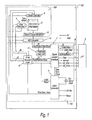
- FIG. 1 is a block diagram of an embodiment of a random access imaging sensor (RAIS) 100.
- RAIS 100 is a circuit that includes a RAIS interface 110, an analog-to-digital (A/D) converter 12 and an active pixel sensor array, i.e., sensor array 105.
- RAIS interface 110 is coupled to conventional data and address buses of an external processor, i.e., a microprocessor 3.
- RAIS interface 110 maps sensor array 105 to an address space of microprocessor 3. Thus, RAIS interface 110 is an interface between microprocessor 3 and sensor array 105.
- Sensor array 105 includes a pixel matrix 2, a row decoder 4, a column decoder 5 and a column charge amplifier 50.
- RAIS interface 110 includes an array decoder 6, an arithmetic logic unit 51, a digital control interface 7, and a clock generator 11.
- Pixel matrix 2 contains a plurality of photosites or pixels for sensing optical images. Pixel matrix 2 is shown herein as an array of 512 x 512 pixels, but pixel matrix 2 may be of any desired dimension.
- the photosensitivity of pixel matrix 2 generates an electron charge proportional to photons incident on pixel matrix 2 and a quantum yield of a photosite 25 (see FIG. 2 ). Each pixel of pixel matrix 2 can be identified by its position in a row and a column of pixel matrix 2.
- Row decoder 4 and column decoder 5 are a configuration of transistor switches that allow the charges on each pixel of pixel matrix 2 to be read out of pixel matrix 2.
- Column charge amplifier 50 amplifies the charges.
- A/D converter 12 receives the amplified charges from charge amplifier 50, converts the charges, and represents the charges as digital values.
- Individual pixels and groups or sub frames of pixels of pixel matrix 2 can be accessed at random through row decoder 4 and column decoder 5. This is accomplished by providing individual pixel reset and readout addresses for rows and columns of pixel matrix 2.
- Digital control interface 7 receives an address from microprocessor 3 and passes the address to array decoder logic 6.
- Array decoder logic 6 accesses a pixel in sensor array 105 based on the address. More specifically, array decoder logic decoder 6 converts the address into a row signal and a column signal that designate a position of a pixel in sensor array 105.
- digital control interface 7 reformats the address from microprocessor 3 for use by array decoder logic 6.
- digital control interface 7 receives two 16-bit address words from microprocessor 3, and reformats the two 16-bit address words into a 32-bit address for array decoder logic 6.
- array decoder logic decoder converts the 32-bit address into a row signal and a column signal that designate a position of a pixel in sensor array 105.
- Array decoder logic 6 drives row decoder 4 and column decoder 5, and provides proper sequencing of row decoder 4 and column decoder 5 based on output signals generated by digital control interface 7 in response to instructions from microprocessor 3.
- Clock generator 11 provides a synchronous clock signal for interfacing with microprocessor 3, and also synchronizes a logic reset, which returns all circuitry in RAIS interface 110 to a known condition.
- RAIS 100 may be implemented with sensor array 105 and RAIS interface 110 being discrete from one another, as shown in FIG. 1 , or as an integrated circuit on a single monolithic semiconductor. Also, the components ofRAIS 100 may be configured of subordinate modules that operate collectively to provide the functionality described herein.
- FIGS. 2 and 3 are schematic circuit diagrams of exemplary embodiments of an active pixel of pixel matrix 2 configured with complementary metal oxide semiconductor (CMOS) devices.
- FIG. 2 shows an active pixel sensor with a photogate over a charge collection well that controls integration time.
- FIG. 3 shows an active pixel sensor that uses a photodiode as a charge collector.
- CMOS complementary metal oxide semiconductor
- photosite 25 is a photosensitive pixel area controlled by changing a voltage applied to a photo gate 10. Photoelectric charge that is collected in photosite 25 can be metered per a discrete time interval. Control of the charge collected under photo gate 10 permits variable integration control of an optical input and is especially useful in scenes with widely varying light levels.
- FIG. 2 also shows an output gate, i.e., OG 20, that limits the charge in the pixel of the channel at photosite 25.
- a floating diffusion 21 includes a source body diode diffusion parasitic capacitance of a reset transistor 22 and a stray layout capacitance. Reset transistor 22 is switched by another transistor, namely transistor 19. Control voltages applied at a row reset bus 17 and a column reset bus 18 cause reset transistor 22 to become active.
- Transistor 19 is selected during pixel initialization to turn on reset transistor 22 and remove the charge collected on floating diffusion 21 from a previous read of pixel charge, thus resetting the pixel.
- This method of resetting the pixel is known as a destructive readout and is selectable through row reset bus 17 and column reset bus 18.
- Reset transistor 22 can affect a single pixel or any number of pixels by the selection of control voltages of row and column reset buses 17 and 18.
- Fig. 3 illustrates a photodiode charge collection pixel.
- charge is collected in a photodiode 28 and is reset in a similar method as described above.
- Transistor 19 is selected during pixel initialization to turn on reset transistor 22 and remove the charge collected on photodiode 28 from a previous read of pixel charge, thus resetting the pixel.
- This method of resetting the pixel is selectable through row reset bus 17 and column-reset bus 18.
- Reset transistor 22 can affect a single pixel or any number of pixels by the selection of control voltages of row and column reset buses 17 and 18.
- the charge collected under photo gate 10 is transferred to floating diffusion 21. This is done by changing the voltage applied on photo gate 10 to cause inversion of photosite 25. This causes the charge to be attracted to floating diffusion 21 in such a way that the charge moves across OG 20 to floating diffusion 21.
- Transistor 24 serves as a source follower to provide current gain of the signal for driving column bus 26.
- Transistor 23 is turned on by application of the RS signal at its gate. This allows current to flow through transistors 24 and 23 to transporting the signal proportional to the charge at the floating diffusion 21, to the column bus 26.
- FIG. 3 illustrates transport of charge to the column bus.
- the photodiode 28 accumulates charge and a voltage proportional to the charge on photodiode 28 is transported to column bus 26 when RS is applied to transistor 23.
- Each pixel in the pixel matrix 2 is connected to a column bus 26 in like fashion.
- RS is selected for all pixels in a row simultaneously, thereby placing charge from all pixels in that row on the column bus simultaneously.
- the voltage placed on each column bus 26 can be read out at that time through the column charge amplifiers 50, or a given pixel may not be reset and charge integration can continue until a later time when there is sufficient signal to warrant readout of that pixel.
- the sequence for each pixel is to reset the pixel, then integrate, readout the pixel to the column bus 26, and finally reset the pixel again to begin the next integration period. Multiple readouts to the column bus 26 can be accomplished without resetting the pixel allowing other pixels in a row to be readout with shorter integration times.
- RAIS 100 For illustration, the operation and structure of RAIS 100 will be described in terms of tracking a moving image sensed by sensor array 105. This is typical of a star tracking application for satellite guidance.
- Digital control interface 7 handles all communication with microprocessor 3.
- Digital control interface 7 provides digitally coded information from pixel matrix 2 to the address bus and data bus of microprocessor 3.
- digital control interface 7 includes a sixteen bit data bus 8 and a sixteen bit bi-directional address bus 9.
- Appropriate signals are generated by digital control interface 7 to prepare microprocessor 3 for receiving data.
- Such signals may include a data valid signal, which is on during data output at data bus 8, and an interrupt signal, which can be used to prepare microprocessor 3 for data transmission from pixel matrix 2.
- Array decoder logic 6 translates the commands received by digital control interface 7 and provides addressing to the row 4 and column 5 decoders that is compatible with pixel matrix 2.
- Acquisition mode is used when a new target is being acquired.
- Array decoder logic 6 starts scanning rows in sequence from the top to the bottom of pixel matrix 2. The simultaneously extracted charges are added together to yield a sum that is compared to a threshold value to determine whether a target image is represented in the selected row.
- a high pass spatial filter (not shown) resides within digital control interface 7 and acts upon the data from pixel matrix 2 to remove background or offset from the data.
- Acquisition discrimination utilizing a high pass spatial filter is known in the art. An example of such a filter is described in U.S. Patent No. 5,260,557 , entitled “Method And Apparatus For Acquisition And Tracking Of Light Sources In A Transient Event Rich Environment", which is incorporated herein in its entirety.
- a threshold is then applied to the amplitude of the data. Any pixel data that exceeds the threshold set during acquisition mode is reported to microprocessor 3. Once this pixel data has exceeded the threshold, microprocessor 3 recognizes the data as a valid target and microprocessor 3 executes the track mode for this target.
- microprocessor 3 provides a start address and an end address of a track window to RAIS interface 110.
- the start address and the end address together, designates a portion of sensor array 105.
- RAIS 100 includes a module that receives the start address and the end address, and uses the start address and the end address to present a sequence of addresses that array decoder logic 6 uses to sequentially access a plurality of pixels in the portion.
- Such a module could be a component of either array decoder logic 6 or digital control interface 7, or yet another component RAIS interface 110 in addition to array decoder logic 6 and digital control interface 7.
- array decoder logic 6 starts a row and column counter internally that causes row decoder 4 and column decoder 5 to increment from the start address to the end address for the track window.
- RAIS 100 is capable of handling multiple track windows. The pixel data from each of the row and column addresses within a valid track window are output to microprocessor 3 for data reduction.
- Pixel matrix 2 may possess excessive offset or gain non-uniformity of individual pixels or columns that interfere with the acquisition or tracking as described above. Since each pixel of pixel matrix 2 has its own amplifier, there can be gain differences in the output signal from one pixel to another. Furthermore, these amplifiers can have offsets that vary from pixel to pixel. There can also be differences of the measured signal from column to column of the pixel matrix 2 that generate artificial signals. In some implementations of pixel matrix 2 these artifacts can become large relative to the electro-optical signal that is being measured at each pixel. Arithmetic logic unit 51 corrects errors relating to offset or gain non-uniformity of pixels.
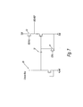
- FIG. 4 is a block diagram of arithmetic logic unit 51.
- Arithmetic logic unit 51 corrects errors relating to offset or gain non-uniformity as the data is transferred back to microprocessor 3 through digital control interface 7.
- Arithmetic logic unit 51 includes a multiplier 62, an adder 65, an accumulator 66, a data register 60, a coefficient register 61, an offset register 64, and a product register 63.
- Pixel data from pixel matrix 2 is run through arithmetic logic unit 51 before entering the digital control interface 7.
- the pixel data is buffered by data register 60.
- a coefficient value that is indexed by the pixel address is provided by microprocessor 3 for correcting the pixel gain, and is buffered in coefficient register 61.
- An offset value that is indexed by the pixel address is provided by microprocessor 3 interface for correcting the pixel offset and is buffered in offset register 64.
- Multiplier 62 takes the contents of data register 60 and the contents of coefficient register 61 and multiplies these values together producing a correction in gain that is stored in product register 63. This product is then advanced to adder 65 where the contents of offset register 64 is added to the value resident in product register 63.
- accumulator 66 The sum of these two digital numbers is then stored in accumulator 66 and scaled to a desired precision.
- the output of accumulator 66 is indicated by the expression a y,x + bx y,x. Note that the expression uses subscripts y and x which correspond to the row decoder 4 and column decoder 5 values for the pixel being read out of pixel matrix 2. In this way, the pixel data is corrected in real time as it passes through RAIS 100.
- Single pixel access is handled by the direct addressing mode.
- the digital control interface 7 receives a y (row) and an x (column) address for a single pixel from microprocessor 3.
- Array decoder logic 6 applies the x and y components of the address to row decoder 4 and column decoder 5, respectively, for this address only, and only data from the single pixel that corresponds to the address is returned to microprocessor 3 through the digital control interface 7 This method is used to control readout or integration of single pixels.
- Row decoder 4 and column decoder 5 can be used in conjunction to reset individual pixels as well.
- the RAIS 100 employs column reset 18 and row reset 17 buses (see FIG. 2 ).
- column reset 18 When column reset 18 is selected, all row reset transistors 19 in a selected column have a bias placed on the drain diffusions. This permits row reset transistors 19 to switch the bias onto the gate of reset transistors 22 in a selected row. In this way the integration time of individual photosites 25 can be controlled independently of other photosites 25 in a given row or column, thus allowing windowed integration time.
- a windowed readout is handled in array decoder logic 6 by state machine logic with a fixed integration time. Up to six windows can be provided for tracking six different targets, such as six stars. This minimizes the amount of data being processed by focusing only on specific regions of interest. Desired window addresses for each of the six windows are passed by microprocessor 3 to RAIS 100.
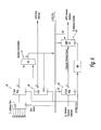
- FIG. 5 is a state diagram of array decoder logic used during windowing operations.
- "X" represents a column address
- Z1 - Z6 are states of the state machine that check the validity of the row or Y address for the window address as defined by microprocessor 3.
- windowing pixel matrix 2 has a rolling blade shutter, i.e., every pixel in a row is reset in sequence from the top to the bottom of pixel matrix 2.
- the state machine After resetting every pixel in a row and before the Y address is advanced to the next row, the state machine interrogates every pixel in that row to determine coincidence with a valid track window. After reading all pixels in a given row that coincide with the valid track window, the next row is reset and the interrogation process begins for the next row.
- the state machine advances to the TRCV state.
- the TRCV state is used to hold the state machine until the track mode has been completed for a given frame. Once the TR flag becomes valid the ADL windowing state machine advances to the next frame by returning to the IDLE state.
- T1 represents the timeout of integration time for the first state called “IDLE”.
- T8 represents the timeout of the second state called “read reset”.
- Z window coordinates are window addresses provided by microprocessor 3.
- the read reset state When the read reset state has completed resetting a row as outlined above, it begins scanning each row for coincidence with the Z window coordinates. If a row address is found that is coincident with the Z window address then column pixel data associated with the Z window address is readout.
- microprocessor 3 provides six Z window addresses or more (although only six are shown in FIG. 5 ) in the row dimension or Y, and are stored in a Y address register 40.
- a Y counter 42 increments through all row addresses.
- Each of these addresses is compared in an address comparator 41 to the Z window addresses stored in Y address register 40. If the row scanned produces a valid comparison between the two inputs of the address comparator 41 then the state machine progresses to a column readout sequence for that Z window address.
- An X address register 43 contains the valid X address for the Z track window that has been validated.
- X address register 43 loads an X address counter 44 for column decoder 5 with a preset so that X address counter 44 starts the readout of this row at the desired column and counts up to the end of the window address.
- the state machine of FIG. 5 progresses to the next Z window address and repeats the process for the next track window address contained in Y address register 40.
- FIG. 6 is a functional block diagram of the logic that scans pixel matrix 2 by row for valid track windows.
- the integration time is selected for each window rather than globally for the entire pixel matrix 2.
- additional logic is employed to control when each window is scanned, and non-destructive readouts are used to preserve the pixel charge in overlapping windows.
- an integration time is defined for each window by microprocessor 3 and is passed to RANIS 100 for setting each of six timers for integration time.
- the readout sequence for that window begins by setting row decoder 4 and column decoder 5, corresponding to the beginning pixel address of the window that has reached its terminal count.
- Each of the pixels within the defined window is then readout to a corresponding window buffer.
- the next window timer is inspected for its terminal count and the sequence will repeat.
- the entire pixel matrix 2 is reset, which defines the beginning of a new integration time or a new frame for all track windows.
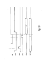
- FIGS. 7 and 8 are schematic diagrams of an exemplary output bus and correlated double sample (CDS) circuits of an active pixel sensor.
- the circuits of FIGS. 7 or 8 would be located within column amplifiers 50, shown in FIG. 1 . These are different configurations for performing CDS of an active pixel sensor.
- FIGS. 9 and 10 illustrate typical pixel timing for a pixel with a photogate present and having a column amplifier circuit topology as shown in FIGS. 7 and 8 , respectively.
- a signal designated as PG is applied to the gate of photogate 10 of pixel matrix 2, and Reset is applied to the gate of transistor 22.
- Reset is high, and the pixel is held Reset by transistor 22.
- Readout of the pixel occurs at the falling edge of PG, which corresponds with a low-level transition at photogate 10.
- Reset is dropped, turning off reset transistor 22. This allows charge to be accumulated on floating diffusion 21.
- photogate 10 is pulsed low (i.e., PG is pulsed low) allowing this charge to transfer from the pixel well or photosite 25, CDS is pulsed on. This turns on CDS transistor 31 ( FIG. 7 ).
- FIG. 8 illustrates another topology of an exemplary output bus and correlated double sample (CDS) circuit of an active pixel sensor in column amplifier 50.
- This is a differential circuit used for sampling each pixel of the selected row and column.
- a sample hold reset (SHR) transistor 34 is turned on to sample the residual floating diffusion charge. That charge is stored on a capacitor 27.
- SHR sample hold reset
- SHS sample hold signal
- RAIS 100 enables microprocessor 3 to address pixel matrix 2 from with in the memory space of microprocessor 3 as microprocessor 3 does with any other peripheral, that is, by direct memory access.
- No large-scale external logic arrays are needed to operate pixel matrix 2, as would be required with conventional CCD technology. Instead, RAIS 100 sits on data bus 8 and address bus 9, and functions similarly to a random access memory in an ordinary microprocessor application.
- images from sensor array 105 appear in a memory map that may be analyzed under software control. This makes the software architecture much less complex than it is with traditional sensor arrays.
- microprocessor 3 may be imbedded in RAIS 100 along with firmware for the desired application.
- RAIS 100 is employed for tracking a target such as a star or other body.
- Microprocessor 3 receives a scan of pixel matrix 2 for comparison to known data in a memory (not shown). Assuming that the target is a star, pixel charges of a desired star magnitude, i.e., brightness, may be identified to determine the column position of the star in a pixel image. Once this has been established a sub-frame of pixels or a "soft window” may be drawn around the star in two dimensions, i.e., in rows and columns, of photosites 25 within pixel matrix 2. Microprocessor 3 provides the start address and end address for a window to array decoder logic 6 through digital control interface 7 for read-out of the sub-frame of pixel matrix 2. After acquisition of a target, the target may be tracked across the field of view of pixel matrix 2.
- Array decoder logic 6 accepts the sub-frame addresses for track windows from digital control interface 7 and provides row and column sequencing to drive row decoder 4 and column decoder 5 for the commanded readout of pixel matrix 2 in either acquisition mode or track mode.
- RAIS 100 is but one of several ways to implement a star tracking application in the context of RAIS 100.
- different active pixel designs may require alteration to the specific circuitry and operation of the software.
- the architecture of RAIS 100 provides flexibility in applications without sacrificing compatibility with various active pixel sensors and microprocessor designs.
- RAIS 100 Since the output data of RAIS 100 is mapped into an address space of microprocessor 3 as memory, and since RAIS 100 includes array decoder logic 6 and appropriate clock references, RAIS 100 can be completely controlled by software.
- An example of software used for tracking moving images is a high level state machine referred to as software control logic (SCL), and is designed to control all the star tracker functions while allowing flexibility in readout and pixel data processing.
- SCL software control logic
- the number of tracked images is a function of the number of SCLs running in microprocessor 3 and is dependent on processing speed and power.
- FIG. 11 is a state diagram of a software state machine for a single SCL.
- the SCL consists of two modes and four states.
- the modes are acquisition mode (AM) and track mode (TM).
- the states are integration time (TI), row scan (RS), column acquisition (CA) and track (TR).
- the flags used to advance the state machine are POR, TM, IC, EX, CS, and WR.
- POR is Power on Reset and causes the state machine to start at TI state after initializing the power to the system.
- TM is Track Mode and is one of two modes as described above.
- IC is the integration time counter and is set at the beginning of TI state at a software programmable value.
- EX is a flag used in the row scan state to indicate when a row has exceeded the software programmable threshold.
- CS column scan and is a flag used to indicate when the readout of the software programmable columns is complete.
- WR is a flag used to determine when a particular target window has been readout. When this flag goes true the machine starts a new integration time for that SCL window. Upon the application of a Power on Reset (POR) the SCL returns to the TI state.
- POR Power on Reset
- the window address is composed of two 24 bit binary numbers that are proportional to the windows starting and ending pixel addresses. These addresses are repeated or updated upon entry to the TR state. This is done for the direct addressing mode, where an integration period sub-frame may be different than the single pixel readout produced by direct addressing.
- the track window or sub-frame can be any dimension from 1 x 1 up to the dimensions of pixel matrix 2, with the latter yielding a full frame output rather than window. Overlap of windows can be handled through special logic in the hardware of RAIS 100.
- Microprocessor 3 can manage a first sub-frame of sensor array 105 and a second sub-frame of sensor array 105 where the first sub-frame has a first integration time and the second sub-frame has a second integration time. Also, the first sub-frame and the second sub-frame may overlap one another.
- the present description relates to a selection of up to six subframes or track windows, it is possible to configure a window for every pixel in the array.
- the ability to select individual window integration periods allows the sensor array system to handle wide dynamic ranges over the full field of view of pixel matrix 2.
- An integration time counter (IC) resides in software and is controlled by a software programmable delay set for a desired integration period. While IC is low the machine dwells in the TI state. The next clock cycle after IC goes true the state machine advances to RS.
- RS row scan
- RAIS interface 110 progresses through columns of sensor array 105 to locate the target.
- a column counter which is software programmable to the number of columns in the array, starts counting down looking for pixel charges in excess of a new threshold set to a level appropriate for a single star.
- SFA window address
- TM mode is initiated. If no excesses occur, TM mode would not be set and the state machine returns to the TI state, but remains in the AM mode, processing another acquisition cycle. The state machine remains in AM mode until a valid TM mode is produced. If TM mode is set, the state machine returns to the TI state to begin a new integration period.
- WR Window Read counter
- TM If at this time TM is still 1, then at the completion of the TI state, the state machine advances to the TR state again for another track window readout. If, however, track was lost during the previous TR state, TM would have gone to 0 and a new acquisition sequence would begin as defined above unless the SCL had been turned off for that track window. In that case the SCL would remain in its reset condition and would not output address words.
- Each track window has its own SCL operating in identical fashion to the description above. Integration periods for each window can be commanded at once, one SCL then the next SCL and so forth. Readout of the windows in the TR state must be handled sequentially. So, if a window is being read out, the next window must not be read out until completion of its predecessor.
- overlapping window addresses these are passed to array decoder logic 6 so a flag can be set to issue non-destructive readouts at the pixels that would overlap in a given track window.
- a non-destructive readout does not reset the given pixel in pixel matrix 2 when that row is addressed.
- an integrated circuit semiconductor chip is constructed having an active pixel sensor array. Each pixel may be independently addressed and reset, driven by a single set of row and column decoders. Array logic provides sequencing instructions to the decoders to scan the array for target discrimination. There is also a capability for correcting gain and offset deficiencies at an individual pixel during readout of the sensor array.
- a digital control interface receives the digital output data from the sensor array and can be handled through direct memory accesses of a microprocessor. The integrated circuit enables the microprocessor to address the sensor array from with in the memory space of the microprocessor.
Abstract
Description
- The present invention relates to imaging technology, and more particularly, to a technique for accessing pixels in an active pixel sensor array. Embodiments of the invention may be used, for example, in cameras and in applications such as star tracking for satellite attitude control.
- A new image sensor technology is being developed as a successor to charge coupled device (CCD) technology. This new technology utilizes complementary metal oxide processing (CMOS) to construct an active pixel sensor (APS) that is responsive to light input over its field of view. An APS is an array of photosensitive elements known as pixels, each pixel possessing simple electrometers capable of converting photoelectric charge to an electrical current that can readily be measured. Each of the pixels can be accessed individually through various addressing schemes. This technology is contrasted to that of CCD technology where each photosensitive element transfers it's charge to the next element in a"bucket brigade"fashion until the charge reaches a common electrometer for the entire CCD that is capable of converting photoelectric charge to an electrical current.
- Star tracking in the past has been accomplished by electronic imaging, typically usingCCDs. However, future celestial tracking space navigation methods impose challenging requirements. Future host spacecraft should be smaller, have less mass, and require less power than present host spacecraft. Therefore, a list of features desired for future star tracking navigation devices includes miniaturization, small mass, and low power consumption. Radiation hardness, high fill factor, high sampling resolution, windowing (random access to pixels within a frame and programmable integration within windows), wide dynamic range (programmable integration time), and real time pixel access are also desirable in an imaging sensor.
- U. S. Patent Application Publication No.
US 2001/0040631 Al to Ewedemi et al . discloses a sensor array with a memory interface. Pixel data from the sensor array is stored in a local memory. An interface is coupled to the local memory and accesses the local memory for exporting the pixel data. The interface does not access the sensor array. The data is most current at a time of transfer of the data from the sensor array to the local memory, and the data ages after the transfer. Consequently, the pixel data may not be sufficiently current for some real-time processing applications. -
WO-02/073951-A US-6509927-B1 suffer from similar problems.WO-02/073951-A -
US-6509927-B1 discloses a programmably addressable image sensor having an integrated address controller for use in an electronic camera, with an image sensor array and an address controller. Pixels in image sensor array are located based on an X address and a Y address, where values XSTART and YSTART are coordinates of a pixel in image sensor array. The address controller can be viewed as memory-mapped, in that particular addresses output on the bus are used to address various registers within the address controller that are to be written into or read from. The address controller receives values for XSTART and YSTART which are loaded into the addressed registers and that are coordinates of a pixel in image sensor array. - There is a need for an apparatus that provides immediate access to data from an active pixel sensor array. Such an apparatus facilitates an interface for a microprocessor to directly map individual pixels of the active pixel sensor array as if the active pixel sensor array were a memory in the microprocessor's address space, without requiring specific memory interface protocols.
- A subject of the invention is a circuit as in
claim 1. A further subject of the invention is an Integrated circuit as inclaims 5. A still further subject of the invention is a system as inclaim 9. - The present invention takes APS technology another step by allowing not only individual addressing of pixels, but also integration control of a single pixel or a group (window) of pixels within the whole array. The present invention provides for a convenient method of addressing individual or groups (windows) of pixels in the array by a microprocessor or controller so the array is mapped in memory space.
-
-
FIG. 1 is a block diagram of a random access imaging sensor in accordance with the present invention, shown as having a separate interface between an active pixel sensor array and a microprocessor. -
FIG. 2 is a schematic circuit diagram of an active pixel sensor, for a pixel in the sensor array ofFIG. 1 , with a photogate over a charge collection well that controls integration time. -
FIG. 3 is a schematic circuit diagram of an active pixel sensor, for a pixel in the sensor array ofFIG. 1 , that uses a photodiode as a charge collector. -
FIG. 4 is a block diagram of an arithmetic logic unit for correcting errors relating to offset or gain non-uniformity. -
FIG. 5 is a state diagram of array decoder logic used during windowing operations in accordance with the present invention. -
FIG. 6 is a block diagram of logic used during windowing operations in the accordance with present invention. -
FIG. 7 is a schematic circuit diagram of an embodiment of output bus and correlated double sample circuitry of an active pixel sensor. -
FIG. 8 is a schematic circuit diagram of another embodiment of output bus and correlated double sample circuitry of an active pixel sensor. -
FIGS. 9 and10 are read reset timing diagrams for a pixel in accordance with the present invention. -
FIG. 11 is a state diagram of a software state machine for tracking moving images, as may be employed by a microprocessor application in accordance with the present invention. -
FIG. 1 is a block diagram of an embodiment of a random access imaging sensor (RAIS) 100. RAIS 100 is a circuit that includes aRAIS interface 110, an analog-to-digital (A/D)converter 12 and an active pixel sensor array, i.e.,sensor array 105.RAIS interface 110 is coupled to conventional data and address buses of an external processor, i.e., a microprocessor 3. -
RAIS interface 110maps sensor array 105 to an address space of microprocessor 3. Thus,RAIS interface 110 is an interface between microprocessor 3 andsensor array 105. -
Sensor array 105 includes a pixel matrix 2, a row decoder 4, acolumn decoder 5 and acolumn charge amplifier 50.RAIS interface 110 includes anarray decoder 6, anarithmetic logic unit 51, adigital control interface 7, and aclock generator 11. - Pixel matrix 2 contains a plurality of photosites or pixels for sensing optical images. Pixel matrix 2 is shown herein as an array of 512 x 512 pixels, but pixel matrix 2 may be of any desired dimension. The photosensitivity of pixel matrix 2 generates an electron charge proportional to photons incident on pixel matrix 2 and a quantum yield of a photosite 25 (see
FIG. 2 ). Each pixel of pixel matrix 2 can be identified by its position in a row and a column of pixel matrix 2. - Row decoder 4 and
column decoder 5 are a configuration of transistor switches that allow the charges on each pixel of pixel matrix 2 to be read out of pixel matrix 2.Column charge amplifier 50 amplifies the charges. A/D converter 12 receives the amplified charges fromcharge amplifier 50, converts the charges, and represents the charges as digital values. Individual pixels and groups or sub frames of pixels of pixel matrix 2 can be accessed at random through row decoder 4 andcolumn decoder 5. This is accomplished by providing individual pixel reset and readout addresses for rows and columns of pixel matrix 2. -
Digital control interface 7 receives an address from microprocessor 3 and passes the address toarray decoder logic 6.Array decoder logic 6 accesses a pixel insensor array 105 based on the address. More specifically, arraydecoder logic decoder 6 converts the address into a row signal and a column signal that designate a position of a pixel insensor array 105. - If necessary,
digital control interface 7 reformats the address from microprocessor 3 for use byarray decoder logic 6. For example, in the embodiment ofRAIS 100 shown inFIG. 1 ,digital control interface 7 receives two 16-bit address words from microprocessor 3, and reformats the two 16-bit address words into a 32-bit address forarray decoder logic 6. In this example, array decoder logic decoder converts the 32-bit address into a row signal and a column signal that designate a position of a pixel insensor array 105. -
Array decoder logic 6 drives row decoder 4 andcolumn decoder 5, and provides proper sequencing of row decoder 4 andcolumn decoder 5 based on output signals generated bydigital control interface 7 in response to instructions from microprocessor 3.Clock generator 11 provides a synchronous clock signal for interfacing with microprocessor 3, and also synchronizes a logic reset, which returns all circuitry inRAIS interface 110 to a known condition. -
RAIS 100 may be implemented withsensor array 105 andRAIS interface 110 being discrete from one another, as shown inFIG. 1 , or as an integrated circuit on a single monolithic semiconductor. Also, thecomponents ofRAIS 100 may be configured of subordinate modules that operate collectively to provide the functionality described herein. -
FIGS. 2 and3 are schematic circuit diagrams of exemplary embodiments of an active pixel of pixel matrix 2 configured with complementary metal oxide semiconductor (CMOS) devices.FIG. 2 shows an active pixel sensor with a photogate over a charge collection well that controls integration time.FIG. 3 shows an active pixel sensor that uses a photodiode as a charge collector. - Referring to
FIG. 2 ,photosite 25 is a photosensitive pixel area controlled by changing a voltage applied to aphoto gate 10. Photoelectric charge that is collected inphotosite 25 can be metered per a discrete time interval. Control of the charge collected underphoto gate 10 permits variable integration control of an optical input and is especially useful in scenes with widely varying light levels. -
FIG. 2 also shows an output gate, i.e.,OG 20, that limits the charge in the pixel of the channel atphotosite 25. A floatingdiffusion 21 includes a source body diode diffusion parasitic capacitance of areset transistor 22 and a stray layout capacitance.Reset transistor 22 is switched by another transistor, namelytransistor 19. Control voltages applied at a rowreset bus 17 and acolumn reset bus 18cause reset transistor 22 to become active. -
Transistor 19 is selected during pixel initialization to turn onreset transistor 22 and remove the charge collected on floatingdiffusion 21 from a previous read of pixel charge, thus resetting the pixel. This method of resetting the pixel is known as a destructive readout and is selectable through row resetbus 17 and column resetbus 18.Reset transistor 22 can affect a single pixel or any number of pixels by the selection of control voltages of row and column resetbuses -
Fig. 3 illustrates a photodiode charge collection pixel. Here charge is collected in aphotodiode 28 and is reset in a similar method as described above.Transistor 19 is selected during pixel initialization to turn onreset transistor 22 and remove the charge collected onphotodiode 28 from a previous read of pixel charge, thus resetting the pixel. This method of resetting the pixel is selectable through row resetbus 17 and column-reset bus 18.Reset transistor 22 can affect a single pixel or any number of pixels by the selection of control voltages of row and column resetbuses - Referring again to
Fig. 2 , during a readout operation of a pixel, the charge collected underphoto gate 10 is transferred to floatingdiffusion 21. This is done by changing the voltage applied onphoto gate 10 to cause inversion ofphotosite 25. This causes the charge to be attracted to floatingdiffusion 21 in such a way that the charge moves acrossOG 20 to floatingdiffusion 21. - Once the charge is resident at floating
diffusion 21 the charge can then be transferred tocolumn bus 26.Transistor 24 serves as a source follower to provide current gain of the signal for drivingcolumn bus 26.Transistor 23 is turned on by application of the RS signal at its gate. This allows current to flow throughtransistors diffusion 21, to thecolumn bus 26. - In a similar fashion,
Fig. 3 illustrates transport of charge to the column bus. Here thephotodiode 28 accumulates charge and a voltage proportional to the charge onphotodiode 28 is transported tocolumn bus 26 when RS is applied totransistor 23. - Each pixel in the pixel matrix 2 is connected to a
column bus 26 in like fashion. RS is selected for all pixels in a row simultaneously, thereby placing charge from all pixels in that row on the column bus simultaneously. The voltage placed on eachcolumn bus 26 can be read out at that time through thecolumn charge amplifiers 50, or a given pixel may not be reset and charge integration can continue until a later time when there is sufficient signal to warrant readout of that pixel. In other words, the sequence for each pixel is to reset the pixel, then integrate, readout the pixel to thecolumn bus 26, and finally reset the pixel again to begin the next integration period. Multiple readouts to thecolumn bus 26 can be accomplished without resetting the pixel allowing other pixels in a row to be readout with shorter integration times. - For illustration, the operation and structure of
RAIS 100 will be described in terms of tracking a moving image sensed bysensor array 105. This is typical of a star tracking application for satellite guidance. -
Digital control interface 7 handles all communication with microprocessor 3.Digital control interface 7 provides digitally coded information from pixel matrix 2 to the address bus and data bus of microprocessor 3. For the exemplary embodiment shown inFIG. 1 ,digital control interface 7 includes a sixteenbit data bus 8 and a sixteen bitbi-directional address bus 9. Appropriate signals are generated bydigital control interface 7 to prepare microprocessor 3 for receiving data. Such signals may include a data valid signal, which is on during data output atdata bus 8, and an interrupt signal, which can be used to prepare microprocessor 3 for data transmission from pixel matrix 2. -
Array decoder logic 6 translates the commands received bydigital control interface 7 and provides addressing to the row 4 andcolumn 5 decoders that is compatible with pixel matrix 2.Array decoder logic 6, when employed for moving target applications, operates in three basic modes, i.e., acquisition mode, tracking mode, and direct addressing mode. - Acquisition mode is used when a new target is being acquired.
Array decoder logic 6 starts scanning rows in sequence from the top to the bottom of pixel matrix 2. The simultaneously extracted charges are added together to yield a sum that is compared to a threshold value to determine whether a target image is represented in the selected row. - Alternatively a high pass spatial filter (not shown) resides within
digital control interface 7 and acts upon the data from pixel matrix 2 to remove background or offset from the data. Acquisition discrimination utilizing a high pass spatial filter is known in the art. An example of such a filter is described inU.S. Patent No. 5,260,557 , entitled "Method And Apparatus For Acquisition And Tracking Of Light Sources In A Transient Event Rich Environment", which is incorporated herein in its entirety. A threshold is then applied to the amplitude of the data. Any pixel data that exceeds the threshold set during acquisition mode is reported to microprocessor 3. Once this pixel data has exceeded the threshold, microprocessor 3 recognizes the data as a valid target and microprocessor 3 executes the track mode for this target. - In the track mode, microprocessor 3 provides a start address and an end address of a track window to
RAIS interface 110. The start address and the end address, together, designates a portion ofsensor array 105.RAIS 100 includes a module that receives the start address and the end address, and uses the start address and the end address to present a sequence of addresses thatarray decoder logic 6 uses to sequentially access a plurality of pixels in the portion. Such a module could be a component of eitherarray decoder logic 6 ordigital control interface 7, or yet anothercomponent RAIS interface 110 in addition toarray decoder logic 6 anddigital control interface 7. Nevertheless,array decoder logic 6 starts a row and column counter internally that causes row decoder 4 andcolumn decoder 5 to increment from the start address to the end address for the track window.RAIS 100 is capable of handling multiple track windows. The pixel data from each of the row and column addresses within a valid track window are output to microprocessor 3 for data reduction. - Pixel matrix 2 may possess excessive offset or gain non-uniformity of individual pixels or columns that interfere with the acquisition or tracking as described above. Since each pixel of pixel matrix 2 has its own amplifier, there can be gain differences in the output signal from one pixel to another. Furthermore, these amplifiers can have offsets that vary from pixel to pixel. There can also be differences of the measured signal from column to column of the pixel matrix 2 that generate artificial signals. In some implementations of pixel matrix 2 these artifacts can become large relative to the electro-optical signal that is being measured at each pixel.
Arithmetic logic unit 51 corrects errors relating to offset or gain non-uniformity of pixels. -
FIG. 4 is a block diagram ofarithmetic logic unit 51.Arithmetic logic unit 51 corrects errors relating to offset or gain non-uniformity as the data is transferred back to microprocessor 3 throughdigital control interface 7.Arithmetic logic unit 51 includes amultiplier 62, anadder 65, anaccumulator 66, adata register 60, acoefficient register 61, an offset register 64, and aproduct register 63. - Pixel data from pixel matrix 2 is run through
arithmetic logic unit 51 before entering thedigital control interface 7. The pixel data is buffered by data register 60. A coefficient value that is indexed by the pixel address is provided by microprocessor 3 for correcting the pixel gain, and is buffered incoefficient register 61. An offset value that is indexed by the pixel address is provided by microprocessor 3 interface for correcting the pixel offset and is buffered in offset register 64.Multiplier 62 takes the contents of data register 60 and the contents ofcoefficient register 61 and multiplies these values together producing a correction in gain that is stored inproduct register 63. This product is then advanced to adder 65 where the contents of offset register 64 is added to the value resident inproduct register 63. The sum of these two digital numbers is then stored inaccumulator 66 and scaled to a desired precision. The output ofaccumulator 66 is indicated by the expression ay,x + bxy,x. Note that the expression uses subscripts y and x which correspond to the row decoder 4 andcolumn decoder 5 values for the pixel being read out of pixel matrix 2. In this way, the pixel data is corrected in real time as it passes throughRAIS 100. - Single pixel access is handled by the direct addressing mode. Here the
digital control interface 7 receives a y (row) and an x (column) address for a single pixel from microprocessor 3.Array decoder logic 6 applies the x and y components of the address to row decoder 4 andcolumn decoder 5, respectively, for this address only, and only data from the single pixel that corresponds to the address is returned to microprocessor 3 through the digital control interface 7This method is used to control readout or integration of single pixels. - Row decoder 4 and
column decoder 5 can be used in conjunction to reset individual pixels as well. To perform the Reset function, theRAIS 100 employs column reset 18 and row reset 17 buses (seeFIG. 2 ). When column reset 18 is selected, all rowreset transistors 19 in a selected column have a bias placed on the drain diffusions. This permits row resettransistors 19 to switch the bias onto the gate ofreset transistors 22 in a selected row. In this way the integration time ofindividual photosites 25 can be controlled independently ofother photosites 25 in a given row or column, thus allowing windowed integration time. - In one embodiment of the present invention a windowed readout is handled in
array decoder logic 6 by state machine logic with a fixed integration time. Up to six windows can be provided for tracking six different targets, such as six stars. This minimizes the amount of data being processed by focusing only on specific regions of interest. Desired window addresses for each of the six windows are passed by microprocessor 3 toRAIS 100. -
FIG. 5 is a state diagram of array decoder logic used during windowing operations. "X" represents a column address, and Z1 - Z6 are states of the state machine that check the validity of the row or Y address for the window address as defined by microprocessor 3. For this configuration of windowing pixel matrix 2 has a rolling blade shutter, i.e., every pixel in a row is reset in sequence from the top to the bottom of pixel matrix 2. After resetting every pixel in a row and before the Y address is advanced to the next row, the state machine interrogates every pixel in that row to determine coincidence with a valid track window. After reading all pixels in a given row that coincide with the valid track window, the next row is reset and the interrogation process begins for the next row. Once the last row in the array is reached the state machine advances to the TRCV state. The TRCV state is used to hold the state machine until the track mode has been completed for a given frame. Once the TR flag becomes valid the ADL windowing state machine advances to the next frame by returning to the IDLE state. - Other flags of interest are the SOR (Start of Read) flag used to indicate the validity of the readout process of the array. T1 represents the timeout of integration time for the first state called "IDLE". T8 represents the timeout of the second state called "read reset".
- In the read reset state, the state machine starts scanning for readout of valid track windows. Z window coordinates are window addresses provided by microprocessor 3. When the read reset state has completed resetting a row as outlined above, it begins scanning each row for coincidence with the Z window coordinates. If a row address is found that is coincident with the Z window address then column pixel data associated with the Z window address is readout. In the exemplary embodiment shown in
FIG. 5 , there are six Z window addresses, Z1-Z6, that can be scanned. Each Z window address is scanned for coincident column address one row at a time. In this manner when windows overlap in column space, the overlapping columns will be read out, repeating the process for each that fall in the Z window address. That is, microprocessor 3 provides six Z window addresses or more (although only six are shown inFIG. 5 ) in the row dimension or Y, and are stored in aY address register 40. A Y counter 42 then increments through all row addresses. Each of these addresses is compared in anaddress comparator 41 to the Z window addresses stored inY address register 40. If the row scanned produces a valid comparison between the two inputs of theaddress comparator 41 then the state machine progresses to a column readout sequence for that Z window address. An X address register 43 contains the valid X address for the Z track window that has been validated. X address register 43 loads anX address counter 44 forcolumn decoder 5 with a preset so that X address counter 44 starts the readout of this row at the desired column and counts up to the end of the window address. The state machine ofFIG. 5 progresses to the next Z window address and repeats the process for the next track window address contained inY address register 40. -
FIG. 6 is a functional block diagram of the logic that scans pixel matrix 2 by row for valid track windows. - In another embodiment of the present invention the integration time is selected for each window rather than globally for the entire pixel matrix 2. When doing this, additional logic is employed to control when each window is scanned, and non-destructive readouts are used to preserve the pixel charge in overlapping windows. Under this condition, an integration time is defined for each window by microprocessor 3 and is passed to RANIS 100 for setting each of six timers for integration time. When one of the six timers has reached its terminal count, the readout sequence for that window begins by setting row decoder 4 and
column decoder 5, corresponding to the beginning pixel address of the window that has reached its terminal count. Each of the pixels within the defined window is then readout to a corresponding window buffer. At the end of this sequence the next window timer is inspected for its terminal count and the sequence will repeat. When all predefined windows have completed readout, the entire pixel matrix 2 is reset, which defines the beginning of a new integration time or a new frame for all track windows. -
FIGS. 7 and8 are schematic diagrams of an exemplary output bus and correlated double sample (CDS) circuits of an active pixel sensor. The circuits ofFIGS. 7 or8 would be located withincolumn amplifiers 50, shown inFIG. 1 . These are different configurations for performing CDS of an active pixel sensor. -
FIGS. 9 and10 illustrate typical pixel timing for a pixel with a photogate present and having a column amplifier circuit topology as shown inFIGS. 7 and8 , respectively. - Referring to
FIG. 9 andFIG. 2 , a signal designated as PG is applied to the gate ofphotogate 10 of pixel matrix 2, and Reset is applied to the gate oftransistor 22. During integration of the pixel, Reset is high, and the pixel is held Reset bytransistor 22. Readout of the pixel occurs at the falling edge of PG, which corresponds with a low-level transition atphotogate 10. Just prior to readout of the pixel, Reset is dropped, turning offreset transistor 22. This allows charge to be accumulated on floatingdiffusion 21. Just beforephotogate 10 is pulsed low (i.e., PG is pulsed low) allowing this charge to transfer from the pixel well orphotosite 25, CDS is pulsed on. This turns on CDS transistor 31 (FIG. 7 ). When this happens, the residual charge (after resetting) on the floatingdiffusion 21 is sampled by capacitor 32 (FIG. 7 ). Whencapacitor 32 is released by turning off the CDS pulse (FIG. 9 ),capacitor 32 has been charged to the equivalent level of floatingdiffusion 21. Next the charge is transferred fromphotosite 25 to floatingdiffusion 21 by pulsingphotogate 10 low. This places the charge on floatingdiffusion 21 of each pixel and this charge will then be ready for reading out throughtransistor 33 of eachcolumn amplifier 50.Photogate 10 can be selected by row and column discriminators within row decoder 4 andcolumn decoder 5. This allows windowed integration time. If no such selection of columns is made within a row then the entire row will be sampled in this manner, in parallel to each of thecolumn amplifiers 50. -
FIG. 8 illustrates another topology of an exemplary output bus and correlated double sample (CDS) circuit of an active pixel sensor incolumn amplifier 50. This is a differential circuit used for sampling each pixel of the selected row and column. Here a sample hold reset (SHR)transistor 34 is turned on to sample the residual floating diffusion charge. That charge is stored on acapacitor 27. When the signal charge for the selected row and column pixel is transferred from the photosite 25 (FIG. 2 ) to the floating diffusion 21 (FIG. 2 ), a sample hold signal (SHS) 35 transistor is turned on and the charge is stored on acapacitor 28. During the readout period each of the selected column amplifiers are read out to a differential amplifier that is shared by the selection ofcolumn output transistors - Referring again to
FIG. 1 ,RAIS 100 enables microprocessor 3 to address pixel matrix 2 from with in the memory space of microprocessor 3 as microprocessor 3 does with any other peripheral, that is, by direct memory access. No large-scale external logic arrays are needed to operate pixel matrix 2, as would be required with conventional CCD technology. Instead,RAIS 100 sits ondata bus 8 andaddress bus 9, and functions similarly to a random access memory in an ordinary microprocessor application. Thus, images fromsensor array 105 appear in a memory map that may be analyzed under software control. This makes the software architecture much less complex than it is with traditional sensor arrays. - If a more specialized application is desired, microprocessor 3 may be imbedded in
RAIS 100 along with firmware for the desired application. - In a "star tracker" application,
RAIS 100 is employed for tracking a target such as a star or other body. Microprocessor 3 receives a scan of pixel matrix 2 for comparison to known data in a memory (not shown). Assuming that the target is a star, pixel charges of a desired star magnitude, i.e., brightness, may be identified to determine the column position of the star in a pixel image. Once this has been established a sub-frame of pixels or a "soft window" may be drawn around the star in two dimensions, i.e., in rows and columns, ofphotosites 25 within pixel matrix 2. Microprocessor 3 provides the start address and end address for a window toarray decoder logic 6 throughdigital control interface 7 for read-out of the sub-frame of pixel matrix 2. After acquisition of a target, the target may be tracked across the field of view of pixel matrix 2. -
Array decoder logic 6 accepts the sub-frame addresses for track windows fromdigital control interface 7 and provides row and column sequencing to drive row decoder 4 andcolumn decoder 5 for the commanded readout of pixel matrix 2 in either acquisition mode or track mode. - The above description is but one of several ways to implement a star tracking application in the context of
RAIS 100. In addition, different active pixel designs may require alteration to the specific circuitry and operation of the software. The architecture ofRAIS 100 provides flexibility in applications without sacrificing compatibility with various active pixel sensors and microprocessor designs. - Since the output data of
RAIS 100 is mapped into an address space of microprocessor 3 as memory, and sinceRAIS 100 includesarray decoder logic 6 and appropriate clock references,RAIS 100 can be completely controlled by software. An example of software used for tracking moving images is a high level state machine referred to as software control logic (SCL), and is designed to control all the star tracker functions while allowing flexibility in readout and pixel data processing. The number of tracked images is a function of the number of SCLs running in microprocessor 3 and is dependent on processing speed and power. -
FIG. 11 is a state diagram of a software state machine for a single SCL. The SCL consists of two modes and four states. The modes are acquisition mode (AM) and track mode (TM). The states are integration time (TI), row scan (RS), column acquisition (CA) and track (TR). The flags used to advance the state machine are POR, TM, IC, EX, CS, and WR. POR is Power on Reset and causes the state machine to start at TI state after initializing the power to the system. TM is Track Mode and is one of two modes as described above. IC is the integration time counter and is set at the beginning of TI state at a software programmable value. EX is a flag used in the row scan state to indicate when a row has exceeded the software programmable threshold. CS is column scan and is a flag used to indicate when the readout of the software programmable columns is complete. WR is a flag used to determine when a particular target window has been readout. When this flag goes true the machine starts a new integration time for that SCL window. Upon the application of a Power on Reset (POR) the SCL returns to the TI state. - In the TI state, and more particularly every time the SCL enters the TI state, two address words are output from the tracking algorithm to update the window coordinates for pixel matrix 2. The window address is composed of two 24 bit binary numbers that are proportional to the windows starting and ending pixel addresses. These addresses are repeated or updated upon entry to the TR state. This is done for the direct addressing mode, where an integration period sub-frame may be different than the single pixel readout produced by direct addressing. The track window or sub-frame can be any dimension from 1 x 1 up to the dimensions of pixel matrix 2, with the latter yielding a full frame output rather than window. Overlap of windows can be handled through special logic in the hardware of
RAIS 100. - If, for example, a star is being tracked and it traverses into a window with a different integration time, that star would be lost. In this case, the software will work off alternate integration periods to continue tracking through the window. This is a special case and will not occur when the star tracker is tracking only stars. This is because prior knowledge of the location of the star being tracked will not allow it to traverse into a different window of a star being tracked with a different integration time.
- Microprocessor 3 can manage a first sub-frame of
sensor array 105 and a second sub-frame ofsensor array 105 where the first sub-frame has a first integration time and the second sub-frame has a second integration time. Also, the first sub-frame and the second sub-frame may overlap one another. - Although the present description relates to a selection of up to six subframes or track windows, it is possible to configure a window for every pixel in the array. The ability to select individual window integration periods allows the sensor array system to handle wide dynamic ranges over the full field of view of pixel matrix 2.
- An integration time counter (IC) resides in software and is controlled by a software programmable delay set for a desired integration period. While IC is low the machine dwells in the TI state. The next clock cycle after IC goes true the state machine advances to RS.
- In the RS state, Acquisition Mode (AM) is operational.
RAIS interface 110 scans throughsensor array 105 to locate a row that includes a target, or a portion of the target. In the RS state, only the row address is given todigital control interface 7.Array decoder logic 6 enables all columns of that row, and all pixels within the row are summed together. The data is then compared to a programmable threshold set to a level commensurate with a target signal compatible with the co-addition of all the columns of a row and only flagged if the data exceeds this threshold. If the during the row scan (RS) the threshold is exceeded (EX=1), the row number is stored and the SCL state machine repeats the row scan to eliminate the possibility of transient events. If EX remains set to one, then the SCL state machine advances to the CA state at the completion of the row scan (RS=1). Upon termination of the row scan counter, the RS flag goes true and if no signal exceeded (EX=0) the threshold in the entire scan, the state machine returns to TI to begin a new integration period. - In the CA state,
RAIS interface 110 progresses through columns ofsensor array 105 to locate the target. Upon entering the CA state, a column counter, which is software programmable to the number of columns in the array, starts counting down looking for pixel charges in excess of a new threshold set to a level appropriate for a single star. After mapping the columns with excesses in a given row, a window address (SFA) is produced and TM mode is initiated. If no excesses occur, TM mode would not be set and the state machine returns to the TI state, but remains in the AM mode, processing another acquisition cycle. The state machine remains in AM mode until a valid TM mode is produced. If TM mode is set, the state machine returns to the TI state to begin a new integration period. This is found by the Boolean expression:
CS is defined as a flag for controlling the state machine. This flag goes true when the last column of a row has been scanned. TI is executed and a readout of the window is begun upon entering the TR state. TI is the state where the integration time is set for a new frame. So after CA a new TI is executed and since CA found a valid star now the track mode TR, is entered. The track window address is passed todigital control interface 7 for interpretation byarray decoder logic 6. Upon termination of a Window Read counter (WR) the SFA is incremented and the state machine advances to the TI state for a new integration period. If at this time TM is still 1, then at the completion of the TI state, the state machine advances to the TR state again for another track window readout. If, however, track was lost during the previous TR state, TM would have gone to 0 and a new acquisition sequence would begin as defined above unless the SCL had been turned off for that track window. In that case the SCL would remain in its reset condition and would not output address words. Each track window has its own SCL operating in identical fashion to the description above. Integration periods for each window can be commanded at once, one SCL then the next SCL and so forth. Readout of the windows in the TR state must be handled sequentially. So, if a window is being read out, the next window must not be read out until completion of its predecessor. In the case of overlapping window addresses, these are passed toarray decoder logic 6 so a flag can be set to issue non-destructive readouts at the pixels that would overlap in a given track window. A non-destructive readout does not reset the given pixel in pixel matrix 2 when that row is addressed. - Thus, an integrated circuit semiconductor chip is constructed having an active pixel sensor array. Each pixel may be independently addressed and reset, driven by a single set of row and column decoders. Array logic provides sequencing instructions to the decoders to scan the array for target discrimination. There is also a capability for correcting gain and offset deficiencies at an individual pixel during readout of the sensor array. A digital control interface receives the digital output data from the sensor array and can be handled through direct memory accesses of a microprocessor. The integrated circuit enables the microprocessor to address the sensor array from with in the memory space of the microprocessor.
- While herein are described several embodiments in accordance with the present invention, it is to be clearly understood that the same are susceptible to numerous changes apparent to one skilled in the art. Therefore, the invention is not to be regarded as being limited to the details shown and described herein, but is intend to encompass all changes and modifications that fall within the scope of the appended claims.
Claims (17)
- Circuit (100) comprising:a decoder (6), characterized in that said decoder (6) comprises:means for receiving a memory address from a processor through an address bus within a memory address space of a processor, andmeans for converting said memory address into a row address and a column address that designate a position of a pixel in an active pixel sensor array (2);a first sub-circuit (4) for converting said row address into a row signal that drives a row of said pixel sensor array (2) within which said pixel is located; anda second sub-circuit (5) for converting said column address into a column signal that drives a column of said active pixel sensor array (2) within which said pixel is located.
- Circuit as in claim 1, characterized in that it further comprises:■ a first module (7) for receiving a start address and an end address that designates a portion of said active pixel sensor array, wherein said module uses said start address and said end address to present a sequence of addresses that said decoder uses to sequentially access a plurality of pixels in said portion; or■ a second module (51) for correcting for a condition selected from the group consisting of: an offset of said pixel, and a gain of said pixel.
- Circuit as in claim 1, characterized in that said pixel is one of a plurality of pixels in said active pixel sensor array, and said circuit provides a signal to simultaneously extract charges from said plurality of pixels; preferably
said plurality of pixels forming a row of pixels in said active pixel sensor array (2). - Circuit as in claim 1, characterized in that said pixel is one of a plurality of pixels in said active pixel sensor array, and in that said circuit provides a signal to simultaneously extract charges from said plurality of pixels; preferably
said charges being added together to yield a sum; more preferably
said circuit further comprising a module for comparing said sum to a threshold value to determine whether a target image is represented by said plurality of pixels. - Integrated circuit comprising a circuit as in claim 1, and an active pixel sensor array (2).
- Integrated circuit as in claim 5, characterized in that it further comprises:■ a first module (7) for receiving a start address and an end address that designates a portion of said active pixel sensor array, wherein said module uses said start address and said end address to present a sequence of addresses that said decoder uses to sequentially access a plurality of pixels in said portion;■ a second module (51) for correcting for a condition selected from the group consisting of: an offset of said pixel, and a gain of said pixel;■ a converter (12) for representing a charge read from said pixel as a digital value; or■ an amplifier (50) for amplifying a charge read from said pixel.
- Integrated circuit as in claim 5, characterized in that:■ said active pixel sensor array (2) is configured of complementary metal oxide semiconductor (CMOS) devices;■■ said pixel comprises an electron well and a gate to control integration time over said electron well; or■ said pixel comprises a photodiode to collect a charge.
- Integrated circuit as in claim 5, characterized in that said active pixel sensor array (2) senses an image, and wherein said integrated circuit (100) is employed for tracking a target in said image; preferably said target is a star.
- System comprising a circuit as in claim 1, characterized in that it further comprises:■ an active pixel sensor array (2);■ a converter (12) for representing a charge read from said pixel as a digital value; and■ a microprocessor (3) for providing said memory address and receiving said digital value,■ said memory address space being a memory address space of said microprocessor, and said decoder (6) mapping said active pixel sensor array (2) to said memory address space.
- System as in claim 9, characterized in that:• said active pixel sensor array (2) is configured of complementary metal oxide semiconductor (CMOS) devices;• or• said microprocessor (3) provides a start address and an end address that designates a portion of said active pixel sensor array, and said system further comprises said first module (7) as in claim 3, that uses said start address and said end address to present a sequence of addresses to said decoder to access pixels in said portion;
- System as in claim 9, characterized in that:• said microprocessor controlling an integration time for a window that includes said pixel;• said microprocessor controls an integration time on a group of pixels of said active pixel sensor array (2); or• said microprocessor addressing a sub-frame of view region of said active pixel sensor array (2).
- System as in claim 9, characterized in that it further comprises:■ said second module (51) as in claim 3, to correct for a condition selected from the group consisting of an offset of said pixel and a gain of said pixel; or■ an amplifier (50) for amplifying a charge read from said pixel.
- System as in claim 9, characterized in that said active pixel sensor array (2) senses an image, and said system is employed for tracking a target in said image; preferably said target is a star.
- System as in claim 9, characterized in that said microprocessor (3) manages a first sub-frame of said active pixel sensor array (2) and a second sub-frame of said active pixel sensor array.
- System as in claim 14, wherein:• said first sub-frame having a first integration time and said second sub-frame having a second integration time, or• said first and second sub-frame of view regions overlap one another.
- Circuit as in claim 1, characterized in that said decoder (6) maps said active pixel sensor array to said memory address space.
- Circuit as in claim 1, characterized in that said decoder (6) employs said row address and said column address to access said pixel.
Applications Claiming Priority (3)
| Application Number | Priority Date | Filing Date | Title |
|---|---|---|---|
| US44443603P | 2003-02-03 | 2003-02-03 | |
| US444436P | 2003-02-03 | ||
| PCT/US2004/002963 WO2004071069A2 (en) | 2003-02-03 | 2004-02-03 | Random access imaging sensor |
Publications (2)
| Publication Number | Publication Date |
|---|---|
| EP1593258A2 EP1593258A2 (en) | 2005-11-09 |
| EP1593258B1 true EP1593258B1 (en) | 2009-04-22 |
Family
ID=32850857
Family Applications (1)
| Application Number | Title | Priority Date | Filing Date |
|---|---|---|---|
| EP04707718A Expired - Lifetime EP1593258B1 (en) | 2003-02-03 | 2004-02-03 | Random access imaging sensor |
Country Status (6)
| Country | Link |
|---|---|
| US (1) | US7223954B2 (en) |
| EP (1) | EP1593258B1 (en) |
| AT (1) | ATE429779T1 (en) |
| DE (1) | DE602004020737D1 (en) |
| DK (1) | DK1593258T3 (en) |
| WO (1) | WO2004071069A2 (en) |
Families Citing this family (33)
| Publication number | Priority date | Publication date | Assignee | Title |
|---|---|---|---|---|
| JP2005312025A (en) * | 2004-04-21 | 2005-11-04 | Magnachip Semiconductor Ltd | Cmos image sensor capable of conducting high-speed analog signal processing |
| TWI237998B (en) * | 2004-06-09 | 2005-08-11 | Via Tech Inc | Operation of imaging-sensing unit and imaging-sensing device with the same |
| US7795577B2 (en) * | 2004-08-25 | 2010-09-14 | Richard Ian Olsen | Lens frame and optical focus assembly for imager module |
| US7916180B2 (en) * | 2004-08-25 | 2011-03-29 | Protarius Filo Ag, L.L.C. | Simultaneous multiple field of view digital cameras |
| US8124929B2 (en) * | 2004-08-25 | 2012-02-28 | Protarius Filo Ag, L.L.C. | Imager module optical focus and assembly method |
| EP1812968B1 (en) | 2004-08-25 | 2019-01-16 | Callahan Cellular L.L.C. | Apparatus for multiple camera devices and method of operating same |
| US7564019B2 (en) | 2005-08-25 | 2009-07-21 | Richard Ian Olsen | Large dynamic range cameras |
| US20070102622A1 (en) * | 2005-07-01 | 2007-05-10 | Olsen Richard I | Apparatus for multiple camera devices and method of operating same |
| US7964835B2 (en) | 2005-08-25 | 2011-06-21 | Protarius Filo Ag, L.L.C. | Digital cameras with direct luminance and chrominance detection |
| US20070258006A1 (en) * | 2005-08-25 | 2007-11-08 | Olsen Richard I | Solid state camera optics frame and assembly |
| US7566855B2 (en) * | 2005-08-25 | 2009-07-28 | Richard Ian Olsen | Digital camera with integrated infrared (IR) response |
| US7582857B2 (en) * | 2006-04-18 | 2009-09-01 | The Trustees Of The University Of Pennsylvania | Sensor and polarimetric filters for real-time extraction of polarimetric information at the focal plane |
| JP4582205B2 (en) * | 2008-06-12 | 2010-11-17 | トヨタ自動車株式会社 | Electric vehicle |
| FR2939919A1 (en) | 2008-12-16 | 2010-06-18 | New Imaging Technologies Sas | MATRIX SENSOR |
| WO2012004928A1 (en) * | 2010-07-08 | 2012-01-12 | パナソニック株式会社 | Image capture device |
| FR2978558B1 (en) * | 2011-07-29 | 2013-07-26 | St Microelectronics Grenoble 2 | METHOD FOR REAL TIME CONTROL OF MATRIX IMAGING DEVICE AND ASSOCIATED DEVICE |
| EP2557391A1 (en) | 2011-08-12 | 2013-02-13 | Leica Geosystems AG | Measuring device for determining the spatial location of a measuring aid |
| GB201117319D0 (en) | 2011-10-06 | 2011-11-16 | Isis Innovation | Active pixel image sensor |
| US9264597B2 (en) * | 2011-11-10 | 2016-02-16 | Altasens, Inc. | Sensor state map for managing operational states of an image sensor |
| FR2997258B1 (en) * | 2012-10-18 | 2016-10-07 | Centre Nat D'etudes Spatiales (Cnes) | DETECTION AND MEASUREMENT SYSTEM COMPRISING AN OPTICAL SENSOR, AND METHODS OF DETECTION AND MEASUREMENT THEREFOR |
| US10515284B2 (en) | 2014-09-30 | 2019-12-24 | Qualcomm Incorporated | Single-processor computer vision hardware control and application execution |
| US9923004B2 (en) | 2014-09-30 | 2018-03-20 | Qualcomm Incorporated | Hardware acceleration of computer vision feature detection |
| US9940533B2 (en) | 2014-09-30 | 2018-04-10 | Qualcomm Incorporated | Scanning window for isolating pixel values in hardware for computer vision operations |
| US20170132466A1 (en) | 2014-09-30 | 2017-05-11 | Qualcomm Incorporated | Low-power iris scan initialization |
| US9838635B2 (en) | 2014-09-30 | 2017-12-05 | Qualcomm Incorporated | Feature computation in a sensor element array |
| US9554100B2 (en) | 2014-09-30 | 2017-01-24 | Qualcomm Incorporated | Low-power always-on face detection, tracking, recognition and/or analysis using events-based vision sensor |
| US10728450B2 (en) | 2014-09-30 | 2020-07-28 | Qualcomm Incorporated | Event based computer vision computation |
| US9762834B2 (en) | 2014-09-30 | 2017-09-12 | Qualcomm Incorporated | Configurable hardware for computing computer vision features |
| US9986179B2 (en) | 2014-09-30 | 2018-05-29 | Qualcomm Incorporated | Sensor architecture using frame-based and event-based hybrid scheme |
| US9704056B2 (en) | 2015-04-02 | 2017-07-11 | Qualcomm Incorporated | Computing hierarchical computations for computer vision calculations |
| US10984235B2 (en) | 2016-12-16 | 2021-04-20 | Qualcomm Incorporated | Low power data generation for iris-related detection and authentication |
| US10614332B2 (en) | 2016-12-16 | 2020-04-07 | Qualcomm Incorportaed | Light source modulation for iris size adjustment |
| US10484624B2 (en) | 2017-07-10 | 2019-11-19 | Semiconductor Components Industries, Llc | Imaging sensors with per-pixel control |
Family Cites Families (13)
| Publication number | Priority date | Publication date | Assignee | Title |
|---|---|---|---|---|
| DE3744128A1 (en) | 1987-12-24 | 1989-07-13 | Heering W Prof Dr | Method and circuit arrangement for programmed triggering of CCD and photodiode matrix arrays |
| US5262871A (en) * | 1989-11-13 | 1993-11-16 | Rutgers, The State University | Multiple resolution image sensor |
| US5296852A (en) * | 1991-02-27 | 1994-03-22 | Rathi Rajendra P | Method and apparatus for monitoring traffic flow |
| US5260557A (en) | 1992-01-31 | 1993-11-09 | Hughes Aircraft Company | Method and apparatus for acquisition and tracking of light sources in a transient event rich environment |
| US6570617B2 (en) * | 1994-01-28 | 2003-05-27 | California Institute Of Technology | CMOS active pixel sensor type imaging system on a chip |
| US5841126A (en) | 1994-01-28 | 1998-11-24 | California Institute Of Technology | CMOS active pixel sensor type imaging system on a chip |
| US6509927B1 (en) * | 1994-12-16 | 2003-01-21 | Hyundai Electronics America Inc. | Programmably addressable image sensor |
| EP1715439A3 (en) * | 1998-11-02 | 2007-10-10 | Datalogic S.P.A. | Device for the acquisition and automatic processing of data obtained from optical codes |
| WO2001038825A1 (en) | 1999-11-23 | 2001-05-31 | California Institute To Technology | Dynamically re-configurable cmos imagers for an active vision system |
| US6985181B2 (en) | 2000-05-09 | 2006-01-10 | Pixim, Inc. | CMOS sensor array with a memory interface |
| JP2003535511A (en) * | 2000-06-01 | 2003-11-25 | アトメル・コーポレイション | Dual mode CMOS integrated imager |
| US6825936B2 (en) * | 2000-08-23 | 2004-11-30 | Lmi Technologies, Inc. | High speed camera based sensors |
| WO2002073951A1 (en) | 2001-03-09 | 2002-09-19 | Fastcom Technology Sa | Device for the extraction of freely-definable image segments from an image sensor |
-
2004
- 2004-02-03 WO PCT/US2004/002963 patent/WO2004071069A2/en active Search and Examination
- 2004-02-03 DE DE602004020737T patent/DE602004020737D1/en not_active Expired - Lifetime
- 2004-02-03 EP EP04707718A patent/EP1593258B1/en not_active Expired - Lifetime
- 2004-02-03 AT AT04707718T patent/ATE429779T1/en not_active IP Right Cessation
- 2004-02-03 US US10/770,642 patent/US7223954B2/en active Active
- 2004-02-03 DK DK04707718T patent/DK1593258T3/en active
Also Published As
| Publication number | Publication date |
|---|---|
| WO2004071069A3 (en) | 2005-03-24 |
| EP1593258A2 (en) | 2005-11-09 |
| DK1593258T3 (en) | 2009-07-27 |
| US20040155175A1 (en) | 2004-08-12 |
| WO2004071069A2 (en) | 2004-08-19 |
| ATE429779T1 (en) | 2009-05-15 |
| US7223954B2 (en) | 2007-05-29 |
| DE602004020737D1 (en) | 2009-06-04 |
Similar Documents
| Publication | Publication Date | Title |
|---|---|---|
| EP1593258B1 (en) | Random access imaging sensor | |
| US7733401B2 (en) | Image capturing apparatus | |
| US9899447B2 (en) | Solid-state imaging device, method for driving the same, and imaging device | |
| EP1177680B1 (en) | Image sensor | |
| US7605855B2 (en) | Dual sensitivity image sensor | |
| US7924337B2 (en) | Dual panel pixel readout in an imager | |
| CN101841664B (en) | Solid-state image capturing apparatus, driving method thereof and electronic apparatus | |
| US9398239B2 (en) | Solid-state imaging device having an enlarged dynamic range, and electronic system | |
| US7154548B2 (en) | Multiplexed and pipelined column buffer for use with an array of photo sensors | |
| KR19990023618A (en) | Solid-state image sensor and driving method thereof | |
| KR101966991B1 (en) | Image pickup unit and image-pickup and display system | |
| EP2760198B1 (en) | Advanced region of interest function for image sensors | |
| US6950131B1 (en) | Simultaneous access and reset system for an active pixel sensor | |
| KR100314801B1 (en) | Apparatus for panning and scaling window in image sensor | |
| WO2001035637A1 (en) | Photosensor system and drive control method thereof | |
| EP2760199B1 (en) | Automatic region of interest function for image sensors | |
| JPH10209868A (en) | A/d converting device | |
| CN106252371A (en) | A kind of radioscopic image sensor and the method for correction image disruption | |
| CN106206637A (en) | A kind of radioscopic image sensor and the method for correction image disruption | |
| US7379101B2 (en) | Photosensor system and drive control method for the same | |
| EP3445039B1 (en) | Detection circuit for photo sensor with stacked substrates | |
| EP1772011B1 (en) | Cmos image sensor | |
| JP4339151B2 (en) | Photoelectric conversion device | |
| JPH022792A (en) | Infrared image pickup element and its driving method | |
| Leach et al. | Noise and readout performance of a multiple-readout CCD controller |
Legal Events
| Date | Code | Title | Description |
|---|---|---|---|
| PUAI | Public reference made under article 153(3) epc to a published international application that has entered the european phase |
Free format text: ORIGINAL CODE: 0009012 |
|
| AK | Designated contracting states |
Kind code of ref document: A2 Designated state(s): AT BE BG CH CY CZ DE DK EE ES FI FR GB GR HU IE IT LI LU MC NL PT RO SE SI SK TR |
|
| AX | Request for extension of the european patent |
Extension state: AL LT LV MK |
|
| 17P | Request for examination filed |
Effective date: 20050902 |
|
| DAX | Request for extension of the european patent (deleted) | ||
| GRAP | Despatch of communication of intention to grant a patent |
Free format text: ORIGINAL CODE: EPIDOSNIGR1 |
|
| GRAS | Grant fee paid |
Free format text: ORIGINAL CODE: EPIDOSNIGR3 |
|
| GRAA | (expected) grant |
Free format text: ORIGINAL CODE: 0009210 |
|
| AK | Designated contracting states |
Kind code of ref document: B1 Designated state(s): AT BE BG CH CY CZ DE DK EE ES FI FR GB GR HU IE IT LI LU MC NL PT RO SE SI SK TR |
|
| REG | Reference to a national code |
Ref country code: GB Ref legal event code: FG4D |
|
| REG | Reference to a national code |
Ref country code: CH Ref legal event code: EP |
|
| REG | Reference to a national code |
Ref country code: IE Ref legal event code: FG4D |
|
| REF | Corresponds to: |
Ref document number: 602004020737 Country of ref document: DE Date of ref document: 20090604 Kind code of ref document: P |
|
| REG | Reference to a national code |
Ref country code: DK Ref legal event code: T3 |
|
| NLV1 | Nl: lapsed or annulled due to failure to fulfill the requirements of art. 29p and 29m of the patents act | ||
| PG25 | Lapsed in a contracting state [announced via postgrant information from national office to epo] |
Ref country code: ES Free format text: LAPSE BECAUSE OF FAILURE TO SUBMIT A TRANSLATION OF THE DESCRIPTION OR TO PAY THE FEE WITHIN THE PRESCRIBED TIME-LIMIT Effective date: 20090802 Ref country code: PT Free format text: LAPSE BECAUSE OF FAILURE TO SUBMIT A TRANSLATION OF THE DESCRIPTION OR TO PAY THE FEE WITHIN THE PRESCRIBED TIME-LIMIT Effective date: 20090822 Ref country code: FI Free format text: LAPSE BECAUSE OF FAILURE TO SUBMIT A TRANSLATION OF THE DESCRIPTION OR TO PAY THE FEE WITHIN THE PRESCRIBED TIME-LIMIT Effective date: 20090422 Ref country code: AT Free format text: LAPSE BECAUSE OF FAILURE TO SUBMIT A TRANSLATION OF THE DESCRIPTION OR TO PAY THE FEE WITHIN THE PRESCRIBED TIME-LIMIT Effective date: 20090422 |
|
| PG25 | Lapsed in a contracting state [announced via postgrant information from national office to epo] |
Ref country code: SI Free format text: LAPSE BECAUSE OF FAILURE TO SUBMIT A TRANSLATION OF THE DESCRIPTION OR TO PAY THE FEE WITHIN THE PRESCRIBED TIME-LIMIT Effective date: 20090422 Ref country code: SE Free format text: LAPSE BECAUSE OF FAILURE TO SUBMIT A TRANSLATION OF THE DESCRIPTION OR TO PAY THE FEE WITHIN THE PRESCRIBED TIME-LIMIT Effective date: 20090722 Ref country code: NL Free format text: LAPSE BECAUSE OF FAILURE TO SUBMIT A TRANSLATION OF THE DESCRIPTION OR TO PAY THE FEE WITHIN THE PRESCRIBED TIME-LIMIT Effective date: 20090422 |
|
| PG25 | Lapsed in a contracting state [announced via postgrant information from national office to epo] |
Ref country code: EE Free format text: LAPSE BECAUSE OF FAILURE TO SUBMIT A TRANSLATION OF THE DESCRIPTION OR TO PAY THE FEE WITHIN THE PRESCRIBED TIME-LIMIT Effective date: 20090422 Ref country code: CZ Free format text: LAPSE BECAUSE OF FAILURE TO SUBMIT A TRANSLATION OF THE DESCRIPTION OR TO PAY THE FEE WITHIN THE PRESCRIBED TIME-LIMIT Effective date: 20090422 Ref country code: RO Free format text: LAPSE BECAUSE OF FAILURE TO SUBMIT A TRANSLATION OF THE DESCRIPTION OR TO PAY THE FEE WITHIN THE PRESCRIBED TIME-LIMIT Effective date: 20090422 |
|
| PG25 | Lapsed in a contracting state [announced via postgrant information from national office to epo] |
Ref country code: SK Free format text: LAPSE BECAUSE OF FAILURE TO SUBMIT A TRANSLATION OF THE DESCRIPTION OR TO PAY THE FEE WITHIN THE PRESCRIBED TIME-LIMIT Effective date: 20090422 |
|
| PLBE | No opposition filed within time limit |
Free format text: ORIGINAL CODE: 0009261 |
|
| STAA | Information on the status of an ep patent application or granted ep patent |
Free format text: STATUS: NO OPPOSITION FILED WITHIN TIME LIMIT |
|
| 26N | No opposition filed |
Effective date: 20100125 |
|
| PG25 | Lapsed in a contracting state [announced via postgrant information from national office to epo] |
Ref country code: BG Free format text: LAPSE BECAUSE OF FAILURE TO SUBMIT A TRANSLATION OF THE DESCRIPTION OR TO PAY THE FEE WITHIN THE PRESCRIBED TIME-LIMIT Effective date: 20090722 |
|
| REG | Reference to a national code |
Ref country code: CH Ref legal event code: PL |
|
| PG25 | Lapsed in a contracting state [announced via postgrant information from national office to epo] |
Ref country code: LI Free format text: LAPSE BECAUSE OF NON-PAYMENT OF DUE FEES Effective date: 20100228 Ref country code: GR Free format text: LAPSE BECAUSE OF FAILURE TO SUBMIT A TRANSLATION OF THE DESCRIPTION OR TO PAY THE FEE WITHIN THE PRESCRIBED TIME-LIMIT Effective date: 20090723 Ref country code: CH Free format text: LAPSE BECAUSE OF NON-PAYMENT OF DUE FEES Effective date: 20100228 Ref country code: MC Free format text: LAPSE BECAUSE OF NON-PAYMENT OF DUE FEES Effective date: 20100301 |
|
| PG25 | Lapsed in a contracting state [announced via postgrant information from national office to epo] |
Ref country code: IE Free format text: LAPSE BECAUSE OF NON-PAYMENT OF DUE FEES Effective date: 20100203 |
|
| PGFP | Annual fee paid to national office [announced via postgrant information from national office to epo] |
Ref country code: IT Payment date: 20120223 Year of fee payment: 9 |
|
| PG25 | Lapsed in a contracting state [announced via postgrant information from national office to epo] |
Ref country code: CY Free format text: LAPSE BECAUSE OF FAILURE TO SUBMIT A TRANSLATION OF THE DESCRIPTION OR TO PAY THE FEE WITHIN THE PRESCRIBED TIME-LIMIT Effective date: 20090422 |
|
| PG25 | Lapsed in a contracting state [announced via postgrant information from national office to epo] |
Ref country code: HU Free format text: LAPSE BECAUSE OF FAILURE TO SUBMIT A TRANSLATION OF THE DESCRIPTION OR TO PAY THE FEE WITHIN THE PRESCRIBED TIME-LIMIT Effective date: 20091023 Ref country code: LU Free format text: LAPSE BECAUSE OF NON-PAYMENT OF DUE FEES Effective date: 20100203 |
|
| PG25 | Lapsed in a contracting state [announced via postgrant information from national office to epo] |
Ref country code: TR Free format text: LAPSE BECAUSE OF FAILURE TO SUBMIT A TRANSLATION OF THE DESCRIPTION OR TO PAY THE FEE WITHIN THE PRESCRIBED TIME-LIMIT Effective date: 20090422 |
|
| PGFP | Annual fee paid to national office [announced via postgrant information from national office to epo] |
Ref country code: DK Payment date: 20130225 Year of fee payment: 10 Ref country code: DE Payment date: 20130227 Year of fee payment: 10 |
|
| PGFP | Annual fee paid to national office [announced via postgrant information from national office to epo] |
Ref country code: BE Payment date: 20130227 Year of fee payment: 10 |
|
| PGFP | Annual fee paid to national office [announced via postgrant information from national office to epo] |
Ref country code: FR Payment date: 20140211 Year of fee payment: 11 |
|
| PGFP | Annual fee paid to national office [announced via postgrant information from national office to epo] |
Ref country code: GB Payment date: 20140129 Year of fee payment: 11 |
|
| BERE | Be: lapsed |
Owner name: GOODRICH CORP. Effective date: 20140228 |
|
| REG | Reference to a national code |
Ref country code: DE Ref legal event code: R119 Ref document number: 602004020737 Country of ref document: DE |
|
| REG | Reference to a national code |
Ref country code: DK Ref legal event code: EBP Effective date: 20140228 |
|
| REG | Reference to a national code |
Ref country code: DE Ref legal event code: R119 Ref document number: 602004020737 Country of ref document: DE Effective date: 20140902 |
|
| PG25 | Lapsed in a contracting state [announced via postgrant information from national office to epo] |
Ref country code: DK Free format text: LAPSE BECAUSE OF NON-PAYMENT OF DUE FEES Effective date: 20140228 Ref country code: DE Free format text: LAPSE BECAUSE OF NON-PAYMENT OF DUE FEES Effective date: 20140902 Ref country code: BE Free format text: LAPSE BECAUSE OF NON-PAYMENT OF DUE FEES Effective date: 20140228 |
|
| GBPC | Gb: european patent ceased through non-payment of renewal fee |
Effective date: 20150203 |
|
| REG | Reference to a national code |
Ref country code: FR Ref legal event code: ST Effective date: 20151030 |
|
| PG25 | Lapsed in a contracting state [announced via postgrant information from national office to epo] |
Ref country code: GB Free format text: LAPSE BECAUSE OF NON-PAYMENT OF DUE FEES Effective date: 20150203 |
|
| PG25 | Lapsed in a contracting state [announced via postgrant information from national office to epo] |
Ref country code: FR Free format text: LAPSE BECAUSE OF NON-PAYMENT OF DUE FEES Effective date: 20150302 |
|
| PG25 | Lapsed in a contracting state [announced via postgrant information from national office to epo] |
Ref country code: IT Free format text: LAPSE BECAUSE OF NON-PAYMENT OF DUE FEES Effective date: 20140203 |