EP1591780B1 - Sensor for detecting fluids, and detection device comprising this sensor - Google Patents
Sensor for detecting fluids, and detection device comprising this sensor Download PDFInfo
- Publication number
- EP1591780B1 EP1591780B1 EP05009247.7A EP05009247A EP1591780B1 EP 1591780 B1 EP1591780 B1 EP 1591780B1 EP 05009247 A EP05009247 A EP 05009247A EP 1591780 B1 EP1591780 B1 EP 1591780B1
- Authority
- EP
- European Patent Office
- Prior art keywords
- detection unit
- sensor
- unit according
- cover
- carrier
- Prior art date
- Legal status (The legal status is an assumption and is not a legal conclusion. Google has not performed a legal analysis and makes no representation as to the accuracy of the status listed.)
- Active
Links
Images
Classifications
-
- G—PHYSICS
- G01—MEASURING; TESTING
- G01N—INVESTIGATING OR ANALYSING MATERIALS BY DETERMINING THEIR CHEMICAL OR PHYSICAL PROPERTIES
- G01N27/00—Investigating or analysing materials by the use of electric, electrochemical, or magnetic means
- G01N27/26—Investigating or analysing materials by the use of electric, electrochemical, or magnetic means by investigating electrochemical variables; by using electrolysis or electrophoresis
- G01N27/403—Cells and electrode assemblies
Landscapes
- Chemical & Material Sciences (AREA)
- Life Sciences & Earth Sciences (AREA)
- Health & Medical Sciences (AREA)
- Biochemistry (AREA)
- General Physics & Mathematics (AREA)
- Electrochemistry (AREA)
- Physics & Mathematics (AREA)
- Analytical Chemistry (AREA)
- Molecular Biology (AREA)
- General Health & Medical Sciences (AREA)
- Chemical Kinetics & Catalysis (AREA)
- Immunology (AREA)
- Pathology (AREA)
- Investigating Or Analyzing Materials By The Use Of Electric Means (AREA)
- Investigating Or Analysing Biological Materials (AREA)
- Automatic Analysis And Handling Materials Therefor (AREA)
- Apparatus Associated With Microorganisms And Enzymes (AREA)
Description
Die vorliegende Erfindung bezieht sich auf einen Sensor mit einem elektrochemischen Sensorarray insbesondere in Form eines Elektrodenareals und auf eine Vorrichtung zur Anwendung in der chemischen oder der biochemischen Analytik. Der Sensor lässt sich zusammen mit Kontaktelementen und geeigneten Fluidverbindungen als Detektionseinheit nutzen, mit der als Teil einer Detektionsvorrichtung Bestandteile von Analyseflüssigkeiten elektrochemisch detektiert werden können. Der Sensor ist im Vergleich zu bekannten Sensoren dieser Art wesentlich kostengünstiger herstellbar. Sowohl die elektrischen als auch die fluidischen Verbindungen lassen sich sehr leicht herstellen und wieder lösen, sodass er auch als austauschbares Einwegelement in diagnostischen Analysegeräten eingesetzt werden kann. Auch ist seine Handhabung sehr bequem.The present invention relates to a sensor having an electrochemical sensor array, in particular in the form of an electrode area, and to a device for use in chemical or biochemical analysis. The sensor can be used together with contact elements and suitable fluid connections as a detection unit with which components of analysis fluids can be detected electrochemically as part of a detection device. The sensor is much cheaper to produce compared to known sensors of this type. Both the electrical and the fluidic connections are very easy to produce and loosen, so that it can also be used as an exchangeable disposable element in diagnostic analyzers. Also, its handling is very convenient.
Die Mikrosystemtechnik und Mikrosensorik hat in den letzten 20 Jahren eine Fülle von biochemischen Chipsensoren entwickelt, die zu einem beträchtlichen Fortschritt in der miniaturisierten Analytik geführt haben. Insbesondere sind hier die auf optischen und elektrochemischen Prinzipien basierende Chipsensoren zu nennen, die mit Technologien aus der Halbleiterfertigung hergestellt werden. Die Verwendung von portablen Geräten für chemische und biochemische Analysen mit solchen Einwegsensoren erfordert einen flexiblen Wechsel des Sensorelements und ggf. zugehöriger Reagenzien. Dabei haben die optischen Systeme produktionstechnische Umsetzung und Markteinführung bereits erfolgreich durchlaufen, aber die meisten elektrischen Systeme sind bisher nicht über das Labormusterniveau hinausgekommen. Während optisch-chemische oder optisch-biochemische Sensorsysteme und optische Biochips kontaktlos mit Lichtstrahlen ausgelesen werden können, muss bei elektrochemisch basierten Chip-Systemen auf dem sehr kleinen Raum einer Chipoberfläche die notwendige elektrische Ankopplung zu entsprechenden Messinstrumenten und die fluidische Ankopplung für die Zuführung von Proben und Flüssigkeit bzw. Reagenzien gleichzeitig realisiert werden.Microsystems technology and microsensors have developed a wealth of biochemical chip sensors over the last 20 years, which has led to significant advances in miniaturized analytics. In particular, here are the based on optical and electrochemical principles chip sensors mentioned that are manufactured with technologies from semiconductor manufacturing. The use of portable devices for chemical and biochemical analyzes with such disposable sensors requires a flexible change of the sensor element and possibly associated reagents. The optical systems have already successfully passed through production technology implementation and market introduction, but most electrical systems have not yet surpassed the laboratory model level. While optical-chemical or optical-biochemical sensor systems and optical biochips can be read contactlessly with light beams, in electrochemically based chip systems in the very small space of a chip surface the necessary electrical coupling to corresponding measuring instruments and the fluidic coupling for the supply of samples and Liquid or reagents are realized simultaneously.
Aus
Bei Einsatz planarer elektrochemischer Sensoren, wie z.B. elektrochemischer Sensoren und Feldeffekt-Transistoren in Siliziumtechnologie oder auch elektrochemischer Sensoren auf polymeren Trägern oder solchen aus Glas, erfordert ein ggf. erforderlich werdender Austausch die gleichzeitige Herstellung bzw. Lösung dieser elektrischen und fluidischen Kontakte. Die elektrische Ankopplung wird in der Regel durch kostenaufwendige Kontaktierung mittels Bonddrähten von den elektrischen Ableitflächen auf den Sensoren oder Chips zu den Leiterbahnen auf konventionellen Leiterplatten bzw. zu den Leiterbahnen auf speziellen Trägem wie Glas oder Polymeren realisiert. Aus dem
Ein anderes System offenbart die eine Diagnoseeinrichtung betreffende Patentanmeldung der Firma Siemens
Die nötige elektrische Verdrahtung und Verpackung des Sensors ist im Detail in der
Ähnlich aufgebaut sind auch die Chipsensoren mit fluidischen Systemen und Ableitkontakten in diagnostischen Modulen im System der Firma Nanogen, San Diego USA, (siehe die
In der bereits erwähnten
Die bisher vorgeschlagenen chemisch-biochemische Analysesysteme mit elektrochemischen Sensoren sind aufgrund der vorstehend erläuterten Baustrukturen bei den zu erwartenden, für die Si-Technologie relativ geringen Stückzahlen nur unter vergleichsweise hohen Fertigungskosten zu realisieren. Sie sind im allgemeinen zu teuer, um als Einzelanalysen-Komponenten oder gar Einwegmaterialien eingesetzt zu werden.The previously proposed chemical-biochemical analysis systems with electrochemical sensors are due to the above-described building structures in the expected, for the Si technology relatively low volumes to realize only with relatively high production costs. They are generally too expensive to be used as single analysis components or even disposable materials.
Aufgabe der Erfindung ist es, eine Detektionseinheit für die Detektion von Inhaltsstoffen von Flüssigkeiten bereitzustellen, deren elektrochemischer Sensor wesentlich kostengünstiger herzustellen ist als bisherige Sensoren. Seine elektrischen Zu- und Ableitkontakte sollen dabei leicht lösbar sein, um ihn leicht handhaben und ggf. auch als Einmalkomponente in einem Analysesystem einsetzen zu können. Die Detektionseinheit soll so ausgestaltet sein, dass sie zusammen mit dem genannten Sensor Inhaltsstoffe von Flüssigkeiten elektrochemisch detektieren kann.The object of the invention is to provide a detection unit for the detection of ingredients of liquids whose electrochemical sensor is much cheaper to produce than previous sensors. His electrical supply and Ableitkontakte should be easily solvable in order to handle it easily and possibly to use as a one-time component in an analysis system can. The detection unit should be designed so that it can electrochemically detect ingredients of liquids together with said sensor.
Die Aufgabe wird durch die Bereitstellung einer Detektionseinheit nach Anspruch 1 gelöst. Der Sensor dieser Einheit ist in der Lage, Inhaltsstoffe von Flüssigkeiten mit Hilfe eines Elektroden-Sensorarrays zu detektieren. Er weist ein Trägerelement und ein darauf angeordnetes, planares oder im Wesentlichen planares Sensorelement auf, auf dessen Oberfläche sich das Sensor-Array befindet. Die Elektroden des Sensor-Arrays sind über elektrisch leitende Verbindungen mit ebenfalls auf der Oberfläche des Sensorelements befindlichen Ableitflächen verbunden, aber ansonsten ohne elektrische Verbindung zum Trägerelement. Das Sensorelement ist in Siliciumtechnologie gefertigt. Günstig ist es, ein Silizium-Chip zu verwenden. Das Trägerelement kann ein billiger, unstrukturierter und kontaktloser Träger sein.The object is achieved by the provision of a detection unit according to claim 1. The sensor of this unit is able to detect ingredients of liquids with the aid of an electrode sensor array. It has a carrier element and a planar or essentially planar sensor element arranged thereon, on the surface of which the sensor array is located. The electrodes of the sensor array are connected via electrically conductive connections with also located on the surface of the sensor element Ableitflächen, but otherwise without electrical connection to the carrier element. The sensor element is manufactured in silicon technology. It is favorable to use a silicon chip. The carrier element may be a cheaper, unstructured and contactless carrier.
Vorzugsweise bilden dünne, elektrisch leitende Metallschichten auf dem Sensorelement sowohl die Elektroden als auch die Ableitflächen. Sie können in Dünnschichttechnologie gefertigt sein, z.B. eingelegt in die Chipfläche oder aufgesputtert oder aufgedampft. Auch die elektrisch leitenden Verbindungen oder Kontakte können in dieser Technologie hergestellt sein. Dabei können alle drei für die Elektrik benötigten Teile integral gefertigt werden. Sie befinden sich dann in der Regel auf einer horizontalen Ebene.Preferably, thin, electrically conductive metal layers on the sensor element form both the electrodes and the deflection surfaces. They can be manufactured using thin-film technology, for example inserted into the chip surface or sputtered or vapor-deposited. Also, the electrically conductive connections or contacts may be made in this technology. All three parts required for the electrical system can be used be made integral. They are then usually on a horizontal plane.
Die elektrische Verbindung zwischen Elektrode und Ableitfläche kann frei auf der Oberfläche des Sensorelements liegen. Vorteilhaft ist es jedoch, sie gegen die Oberfläche des Sensorelements zu isolieren. Dies kann beispielsweise durch Aufbringen eines anorganischen, anorganisch-organischen oder organischen isolierenden Materials, z.B. von Siliziumoxid oder einem Silicium-Oxynitrid oder einem Kunststoff wie z.B. einem Lack, erfolgen. Stattdessen kann die elektrisch leitende Verbindung zwischen Elektroden und Ableitflächen in halbleiterüblicher Technologie z.B. über CMOS-Schaltungen hergestellt werden. Dabei erfolgt die elektrische Verbindung von den Elektroden in das Siliziummaterial hinein durch eine isolierende Zwischenschicht zu chipüblichen Strukturen wie z.B. Transistorschaltungen in CMOS-Technologie, die z.B. als aktive Meßschaltungen für jede Arrayelektrode arbeiten können. Von diesen integrierten Strukturen wird wieder eine elektrische Durchführung an die Oberfläche zu den Ableitflächen eingerichtet. Die fluidische und die elektrische Ankopplung ist damit für beide Sensortypen identisch.The electrical connection between the electrode and the discharge surface can lie freely on the surface of the sensor element. However, it is advantageous to isolate them against the surface of the sensor element. This can be done for example by applying an inorganic, inorganic-organic or organic insulating material, for example of silicon oxide or a silicon oxynitride or a plastic such as a paint. Instead, the electrically conductive connection between electrodes and Ableitflächen can be prepared in semiconductor-standard technology, for example via CMOS circuits. The electrical Connection from the electrodes into the silicon material through an insulating interlayer to on-chip structures such as transistor circuits in CMOS technology, for example, can work as active measuring circuits for each array electrode. From these integrated structures, an electrical feedthrough to the surface to the discharge surfaces is established again. The fluidic and electrical coupling is thus identical for both sensor types.
In beispielhaften Ausgestaltungen, z.B. wenn klassische Si-Dünnfilmtechnologie für seine Herstellung eingesetzt wird, kann das Sensorelement Abmessungen im Bereich von etwa 3x3 mm bis 10×10 mm aufweisen. Davon werden üblicherweise ca. 1 x3 mm für das Elektrodenareal (Elektrodenarray) verwendet. Die Form der metallischen Ableitflächen kann beliebig gewählt werden; sie können z.B. kreisförmig oder rechteckig sein. Ihre Dimensionen liegen üblicherweise im Bereich von ca. 0,1 mm2 bis 2mm2, vorzugsweise bis 1mm2. Es soll aber betont werden, dass dies alles nur Beispiele sind; die Größe des Sensors und seiner Bestandteile kann natürlich entsprechend der vorgesehenen Verwendungsart frei gewählt werden.In exemplary embodiments, eg when classical Si thin film technology is used for its fabrication, the sensor element may have dimensions in the range of about 3x3 mm to 10x10 mm. Of these, about 1 x 3 mm are usually used for the electrode area (electrode array). The shape of the metallic Ableitflächen can be chosen arbitrarily; they can be circular or rectangular, for example. Their dimensions are usually in the range of about 0.1 mm 2 to 2mm 2 , preferably to 1mm 2 . It should be emphasized, however, that these are all examples; The size of the sensor and its components can of course be chosen freely according to the intended use.
Die Anzahl der im Sensor-Array vorhandenen Elektroden kann entsprechend dem vorgesehenen Zweck frei gewählt werden. Günstig ist es, mehrere gleichsinnige Elektroden vorzusehen, um mehrere Untersuchungen (sei es zur Detektion verschiedener Substanzen, sei es zur Untersuchung verschiedener Proben auf dieselbe Substanz) gleichzeitig bzw. parallel vornehmen zu können. Die für elektrochemische Sensoren üblichen Hilfselektroden, z.B. Gegen- und/oder Referenzelektroden, können ebenfalls auf den Sensoren angeordnet werden.The number of electrodes present in the sensor array can be freely selected according to the intended purpose. It is advantageous to provide a plurality of electrodes in the same direction in order to be able to carry out a plurality of examinations (whether for the detection of different substances or for the examination of different samples for the same substance) simultaneously or in parallel. The auxiliary electrodes customary for electrochemical sensors, e.g. Counter and / or reference electrodes can also be placed on the sensors.
Der Sensor ist mit der Abdeckung kombiniert, mit der zusammen er die Detektionseinheit bildet, die in Verbindung mit einem Analysengerät als Detektionsvorrichtung Inhaltsstoffe von Flüssigkeiten, insbesondere von solchen biologischer Herkunft, detektieren kann.The sensor is combined with the cover, with which it forms the detection unit, which can detect in combination with an analyzer as a detection device ingredients of liquids, especially those of biological origin.
Die Abdeckung ist so ausgestaltet, dass sie zusammen mit dem Sensor einen oder ggf. mehrere Hohlräume über dem Teil der Oberfläche des Sensorelements bildet, auf dem sich die Fläche oder zumindest eine Teilfläche einer oder mehrerer Elektroden (letzterer Fall z.B. für die Untersuchung eines Fluids auf mehrere Inhaltsstoffe) befindet. Mindestens ein Flüssigkeitskanal in der Abdeckung schafft eine Flüssigkeitsverbindung von mindestens einem der Hohlräume durch die Abdeckung hindurch. Dieser Flüssigkeitskanal kann mit Vorrichtungen zum Zuführen und Absaugen von Flüssigkeiten in den jeweiligen Hohlraum verbunden werden oder kann mit einem Septum verschlossen sein, das sich mit einer Hohlnadel durchstechen lässt, um Flüssigkeit einzuführen oder abzuziehen. Alternativ können zwei Flüssigkeitsverbindungen pro Hohlraum vorgesehen sein, von denen eine als Zufluss und eine als Abfluss fungiert. Der Sensor kann mit der Abdeckung zusammen dann als Durchfluss-Messzelle genutzt werden.The cover is designed such that it forms together with the sensor one or possibly more cavities over the part of the surface of the sensor element on which the surface or at least a partial surface of one or more electrodes (the latter case eg for the examination of a fluid on several ingredients). At least one fluid channel in the cover provides fluid communication of at least one of the cavities through the cover. This liquid channel can be connected to devices for supplying and suction of liquids in the respective cavity or can with a Closed septum, which can be pierced with a hollow needle to introduce or withdraw liquid. Alternatively, two fluid connections can be provided per cavity, one of which acts as an inflow and one as an outflow. The sensor can then be used together with the cover as a flow measuring cell.
Zusätzlich kann auch ein größerer Hohlraum in der Abdeckung als Sammelgefäß für nicht mehr benötigte Meß- und/oder Probenflüssigkeiten ausgebildet sein und ggf. mit Druck-Ausgleichsöffnungen nach außen versehen werden.In addition, a larger cavity in the cover can be designed as a collecting vessel for no longer required measuring and / or sample liquids and possibly provided with pressure equalization openings to the outside.
In einer anderen Ausbildung können Hohlräume und Kanäle wahlweise auch in dem Sensorträger mit Verbindung zu Hohlräumen und oder Kanälen in der Abdeckung angeordnet werden.In another embodiment, cavities and channels can optionally also be arranged in the sensor carrier with connection to cavities and or channels in the cover.
Auf dem Sensor selbst ist in der Regel nur das Elektrodenareal (Sensor-Array) für den Kontakt mit Flüssigkeit vorgesehen. Die elektrische Verbindung zwischen den Elektroden und den Ableitflächen sollte dagegen davon freigehalten werden. Entweder auf dem Sensor und/oder auf der Abdeckung sind deshalb in bevorzugter Weise Dichtungselemente vorgesehen. Insbesondere dann, wenn der Sensor als Einwegmaterial, die Abdeckung aber wiederholt verwendet werden sollen, ist es wünschenswert, den Sensor von allen nicht unbedingt notwendigen Komponenten freizuhalten und diese ggf. in die Abdeckung zu integrieren. Deshalb ist es bevorzugt, dass die Dichtungselemente an der Abdeckung angebracht sind. Es kann sich dabei beispielsweise um O-Ringe oder Dichtfolien handeln. In ganz bevorzugter, aber nicht zwingender Weise sind der Hohlraum und die Dichtungselemente so gestaltet, dass die Flüssigkeit nur die Elekrodenoberfläche berühren kann, aber keine sonstigen Sensorelement-Oberflächen. Die Dichtungselemente setzen dann bevorzugt auf den Randbereichen der Elektrodenflächen oder dicht daneben auf.As a rule, only the electrode area (sensor array) for contact with liquid is provided on the sensor itself. The electrical connection between the electrodes and the Ableitflächen should, however, be kept free of it. Either on the sensor and / or on the cover sealing elements are therefore provided in a preferred manner. In particular, when the sensor is to be used as a disposable material, but the cover repeatedly, it is desirable to keep the sensor of all components not essential and possibly integrate this in the cover. Therefore, it is preferable that the seal members are attached to the cover. These may be, for example, O-rings or sealing foils. Most preferably, but not necessarily, the cavity and the sealing elements are designed so that the liquid can only touch the electrode surface, but no other sensor element surfaces. The sealing elements then preferably set on the edge regions of the electrode surfaces or close to it.
Die Abdeckung weist außerdem elektrische Kontaktelemente zur Herstellung lösbarer elektrischer Verbindungen auf, die mechanisch auf die Ableitflächen des Sensors aufgesetzt werden können. Über diese elektrischen Kontaktelemente können die Elektroden auf der Oberfläche des Sensorelements von außen abgefühlt werden. Die Zahl der Kontaktelemente entspricht in der Regel der Zahl der Ableitflächen und damit der Elektroden.The cover also has electrical contact elements for the production of detachable electrical connections, which can be mechanically placed on the discharge surfaces of the sensor. About these electrical contact elements, the electrodes can be sensed on the surface of the sensor element from the outside. The number of contact elements usually corresponds to the number of Ableitflächen and thus the electrodes.
Die Abdeckung sollte so ausgestaltet sein, dass ihre Verbindung mit dem Sensor wieder gelöst werden kann. Zu diesem Zweck kann sie beispielsweise eine Klapp-, Hebel- oder Klickvorrichtung umfassen, mit der sie mit dem Sensor verbunden und von ihm getrennt werden kann. Diese kann mit dem Träger verbunden sein oder integraler Bestandteil des Trägers sein. Alternativ wird sie ausschließlich durch Druckkräfte auf dem Sensor gehalten.The cover should be designed so that its connection to the sensor can be released again. For this purpose, it can, for example, a folding, Lever or click device include, with which it can be connected to the sensor and disconnected from it. This may be associated with the carrier or be an integral part of the carrier. Alternatively, it is held solely by pressure forces on the sensor.
Die elektrischen Kontaktelemente bestehen im einfachsten Fall aus einem Metallstift, der mechanisch auf die Kontaktfläche gedrückt wird und der reversibel beliebig oft wieder gelöst werden kann. Dadurch wird die sonst übliche fest installierte Kontaktierung z.B. Bondung der metallischen Ableitflächen auf den Chips zu Leiterbahnen auf Chipträgern bzw. Substraten überflüssig. Vorteilhaft ist auch die Verwendung von gefederten Nadelkontakten, die in verschiedenen Ausführungen z.B. mit Durchmessern von 0,8mm erhältlich sind, als Kontaktelement. Ebenso können einfache Federkontakte, wie sie in Miniatursteckern Verwendung finden, zur direkten elektrischen Kontaktierung angewendet werden.The electrical contact elements consist in the simplest case of a metal pin which is mechanically pressed onto the contact surface and can be reversibly as often as desired dissolved again. As a result, the otherwise permanently installed contacting, e.g. Bonding of the metallic Ableitflächen on the chips to tracks on chip carriers or substrates superfluous. Also advantageous is the use of spring-loaded needle contacts, which are available in various designs, e.g. Available with diameters of 0.8mm, as a contact element. Likewise, simple spring contacts, such as those used in miniature connectors, can be used for direct electrical contacting.
In einer besonderen Ausgestaltung der Erfindung finden folienartige elektrisch leitende Kunststoffe oder auch elastische Kunststoffe mit metallisch leitenden Strukturen als reversible Mikrokontakte Verwendung.In a particular embodiment of the invention are film-like electrically conductive plastics or elastic plastics with metallic conductive structures as reversible micro-contacts use.
In allen diesen Fällen können die Kontaktelemente gegebenenfalls zusammen oder in Gruppen von einem isolierenden Halter gehalten werden.In all these cases, the contact elements may optionally be held together or in groups by an insulating holder.
Auf Wunsch können die elektrischen Kontaktelemente oder ein Teil oder eine Gruppe davon auch zusammen mit dem bzw. den Flüssigkeitskanälen der lösbaren Abdeckung in einer gemeinsamen mechanischen Halterung angeordnet sein.If desired, the electrical contact elements or a part or a group thereof can also be arranged together with the liquid channel (s) of the detachable cover in a common mechanical holder.
In einer alternativen grundlegenden Ausgestaltung der Erfindung ist das Abdeckungselement bereits Bestandteil des Sensors und mit diesem fest verbunden. Es bildet mit einer entsprechenden Oberfläche des Sensorelements den Hohlraum, in dem sich die Fläche oder eine Teilfläche mindestens einer der Elektroden, aber keine Ableitfläche befindet. Der Hohlraum kommuniziert mit einer Befüllungsöffnung für Flüssigkeiten. Bezüglich der Zahl und Anordnung des oder der Hohlräume und des darunter liegenden Elektrodenareals gilt das gleiche, was oben für den bzw. die Hohlräume aus Sensor und lösbarer Abdeckung gesagt wurde. In vergleichbarer Weise kann auch zusätzlich eine Flüssigkeits-Ableitung im Abdeckungselement vorgesehen sein, um die Kombination aus Sensor und fest installiertem Abdeckungselement nach Art einer Durchflusszelle betreiben zu können.In an alternative basic embodiment of the invention, the cover element is already part of the sensor and firmly connected thereto. It forms with a corresponding surface of the sensor element, the cavity in which the surface or a partial surface of at least one of the electrodes, but no Ableitfläche is. The cavity communicates with a filling opening for liquids. With regard to the number and arrangement of the cavity or cavities and the electrode area underneath, the same applies to what has been said above for the cavity (s) of sensor and detachable cover. In a comparable manner, a liquid discharge can also be provided in the cover element in order to be able to operate the combination of sensor and permanently installed cover element in the manner of a flow cell.
Das Abdeckungselement ist auf dem Trägerelement und/oder auf dem Sensorelement befestigt, beispielsweise durch Klebeverbindungen oder Heißsiegeln oder elastische Dichtungen. Durch diese Befestigung ist insbesondere der Hohlraum über den Elektroden gegen die restliche Sensorfläche abgedichtet und sind somit die elektrischen Ableitflächen vor Kurzschlüssen geschützt. Im Bereich der Ableitfläche(n) weist das Abdeckungselement eine Aussparung auf, so dass die Ableitflächen von oben offen zugänglich sind.The cover element is fastened on the carrier element and / or on the sensor element, for example by adhesive bonds or heat seals or elastic seals. As a result of this attachment, in particular the cavity above the electrodes is sealed against the remaining sensor surface, and thus the electrical discharge surfaces are protected against short-circuits. In the region of the discharge surface (s), the cover element has a recess, so that the discharge surfaces are openly accessible from above.
Nachteil dieser Ausgestaltung ist, dass der Aufwand zur Herstellung des Sensors höher ist, indem ein zusätzliches Teil, z.B. in konventioneller Spritzguss-Technologie gefertigt und montiert werden muss. Sie besitzt aber besondere Vorteile. So können innerhalb des Abdeckungselements Strukturen vorgesehen sein, die die Anzahl der erforderlichen Arbeitsschritte für die Detektion senkt und das Vorhalten von standardisierten Messlösungen und/oder die jeweils frische Herstellung wenig stabiler Lösungen überflüssig macht. So kann zwischen der oder einigen oder jeder Befüllungsöffnung und dem Hohlraum ein Befüllungskanal vorgesehen sein, der Vorratsnischen zur Aufnahme von Vorratsreagenzien aufweisen kann.Disadvantage of this embodiment is that the effort for the production of the sensor is higher by an additional part, e.g. must be manufactured and assembled using conventional injection molding technology. But it has special advantages. Thus, structures can be provided within the cover element, which reduces the number of required steps for detection and makes the provision of standardized measurement solutions and / or the respectively fresh production of less stable solutions superfluous. Thus, between the or some or each filling opening and the cavity, a filling channel may be provided which may have storage niches for receiving supply reagents.
Die Vorratsreagenzien können flüssig sein. Alternativ sind sie, fest und können beim Befüllungsvorgang aufgelöst und in den Hohlraum über den Elektroden transportiert werden. Hier oder vorher können chemische oder biochemische Reaktionen, die für den analytischen Vorgang, z.B. ein biochemisches Assay, notwendig sind, stattfinden. Optional sind Befüllungsöffnungen, Befüllungskanäle und Hohlräume für flüssige und/oder feste Reagenzien mehrfach in der Abdeckung vorhanden.The stock reagents can be liquid. Alternatively, they are solid and can be dissolved during the filling process and transported into the cavity above the electrodes. Here or before, chemical or biochemical reactions that may be required for the analytical process, e.g. a biochemical assay, necessary to take place. Optionally, filling openings, filling channels and cavities for liquid and / or solid reagents are present in the cover several times.
Die Bereitstellung von baugleichen Sensoren mit verschiedenen Reagenzien im Einwegelement ermöglicht die kosteneffektive Bestimmung verschiedener Zielsubstanzen, wie sie vor allem in der biochemischen Analytik mit ihrer großen Zahl von molekularen Alternativen und Affinitätsbindungen gefordert ist.The provision of identical sensors with different reagents in the disposable element enables the cost-effective determination of various target substances, as required especially in biochemical analysis with its large number of molecular alternatives and affinity binding.
Die Hohlräume können typischer Weise z.B. Volumina zwischen 1-100µl haben, während die Befüllungskanäle in der Regel Durchmesser zwischen 0,1 - 0,5mm haben. Probenvolumina und Flüssigkeitsportionen sind auf diese Dimensionen bezogen typischerweise 1 - 500µl groß. Die übrigen Dimensionen entsprechen den Werten, die für die oben beschriebene Kombination von Sensor und lösbarer Abdeckung angegeben sind.The cavities may typically have volumes between 1-100μl, for example, while the fill channels typically have diameters between 0.1-0.5mm. Sample volumes and liquid portions are typically 1-500μl in terms of these dimensions. The remaining dimensions correspond to the values given for the sensor and detachable cover combination described above.
Wenn die Vorratsreagenzien flüssig sind, können Gase zu ihrem Transport verwendet werden. Alternativ kann eine elastische Membran in der Abdeckung über dem oder den Hohlräumen angebracht sein, die für einen hydraulischen Transport von in den Vorratsnischen gelagerten Flüssigkeiten verwendet werden kann. Wenn die Vorratsreagenzien fest sind, können sie beim Befüllen der Kanäle aufgelöst werden. Vor allem für derartige Fälle ist die erwähnte alternative grundlegende Ausgestaltung mit Flüssigkeits-Ableitung für den Hohlraum über einer/mehreren/allen Elektroden bzw. Teilbereichen dieser Elektroden , aber ggf. auch anderen, zusätzlichen Hohlräumen bzw. Kanälen günstig, um so in einfacher Weise Reaktions-, Spül- und Messschritte vornehmen zu können.If the stock reagents are liquid, gases may be used to transport them. Alternatively, an elastic membrane may be mounted in the cover over the cavity or cavities which may be used for hydraulic transport of liquids stored in the storage niches. If the stock reagents are solid, they can be dissolved when filling the channels. Especially for such cases, the aforementioned alternative basic design with liquid discharge for the cavity over one / more / all electrodes or portions of these electrodes, but possibly also other, additional cavities or channels low, so in a simple way reaction , Rinsing and measuring steps.
Wird ein Sensor gemäß der alternativen Ausgestaltung der Erfindung eingesetzt, ist das einzig zwingend erforderliche zusätzliche Element für die gesamte Detektionseinheit im obigen Sinne ein elektrisches Kontaktelement pro Ableitfläche des Sensors, das mechanisch auf diese aufgesetzt werden kann. Die Flüssigkeitszu- und Abführung muss nicht im selben Element untergebracht sein, das diese(s) Kontaktelement(e) hält. Es ist aber möglich, einen Träger hierfür vorzusehen, der außerdem die entsprechende Anzahl von Durchflusskanälen aufweist, die für die Versorgung des bzw. der die Messzelle(n) bildenden Hohlraums/Hohlräume notwendig sind. Diese Durchflusskanäle sind in bevorzugter Weise mit Dichtungselementen versehen, um z.B. beim Zusammendrücken der genannten Teile eine lösbare, aber dichte Verbindung zwischen Durchflusskanal und Befüllungsöffnung zu gewährleisten. Alternativ können sie beispielsweise als Schlauch ausgestaltet sein, der auf die Befüllungsöffnung der Abdeckung aufgesteckt werden kann oder umgekehrt.If a sensor is used according to the alternative embodiment of the invention, the only absolutely necessary additional element for the entire detection unit in the above sense is an electrical contact element per discharge surface of the sensor, which can be mechanically placed on this. The liquid inlet and outlet must not be housed in the same element holding this contact element (s). However, it is possible to provide a carrier for this, which also has the appropriate number of flow channels, which are necessary for the supply of the or the measuring cell (s) forming cavity / cavities. These flow channels are preferably provided with sealing elements, e.g. to ensure a releasable, but tight connection between the flow channel and filling opening during compression of said parts. Alternatively, they may for example be designed as a hose which can be plugged onto the filling opening of the cover or vice versa.
Auch bei dieser Ausgestaltung der Erfindung können die oben angeführten optionalen Ausführungen realisiert sein, z.B. eine oder mehrere Halterungen für die elektrischen Kontaktelemente und/oder den/die Durchflusskanäle, das Vorsehen einer Klapp-, Hebel- oder Klickvorrichtung oder dergleichen.Also in this embodiment of the invention, the above-mentioned optional embodiments can be realized, for example, one or more holders for the electrical contact elements and / or the / the flow channels, the provision of a folding, lever or click device or the like.
Die beigefügten Figuren zeigen beispielhafte Ausgestaltungen der Erfindung, wobei
-
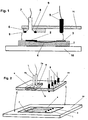
Fig. 1 : den Schnitt durch ein Sensor-Array mit mechanischem Element zur Herstellung lösbarer elektrischer Kontakte in Kombination mit einer lösbaren Abdeckung zur Befüllung mit Flüssigkeiten zeigt, -
Fig. 2 : die Draufsicht auf ein Sensor-Array auf einem Trägerelement und ein zugehöriges mechanisches Element zur gleichzeitigen Herstellung elektrischer Kontakte neben einer Abdeckung zur Befüllung mit Flüssigkeiten zeigt, und -
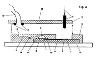
Fig. 3 : den Schnitt durch ein Sensor-Array mit einer fest fixierten Abdeckung und ein zugehöriges mechanisches Element zur gleichzeitigen Herstellung elektrischer Kontakte neben der Befüllung mit Flüssigkeiten zeigt.
-
Fig. 1 Figure 1 shows the section through a sensor array with mechanical element for the production of detachable electrical contacts in combination with a detachable cover for filling with liquids, -
Fig. 2 FIG. 2 shows the plan view of a sensor array on a carrier element and an associated mechanical element for the simultaneous production of electrical contacts next to a cover for filling with liquids, and FIG -
Fig. 3 Fig. 1 shows the section through a sensor array with a fixed fixed cover and an associated mechanical element for the simultaneous production of electrical contacts in addition to the filling with liquids.
Mit der erfindungsgemäßen Kombination aus Sensor und Abdeckung lässt sich ein System schaffen, das insbesondere den raschen Austausch der vor allem in der biochemischen Analytik als Einwegelemente benötigten elektrochemischen Sensor-Arrays ermöglicht. Durch Herstellung lösbarer elektrischer Verbindungen direkt auf dem Sensorelement selbst können bisher notwendige fest installierte elektrische Verbindungen zwischen dem Sensorelement und dem Träger, wie man es von Si-Chips auf Leiterkarten oder anderen Leiterbahnen, z.B. in Form von Bondverbindungen, kennt, entfallen und damit erheblicher technologischer Aufwand eingespart werden, wobei gleichzeitig auch die Realisierung der Zu- und Ableitung zu bzw. von den Elektroden extrem einfach gestaltet ist. Erfindungsgemäß lässt sich ein Sensorelement in einfacher Dünnfilm- Chiptechnik realisieren, was außer den besonders geeigneten Si-Chips auch die Verwendung einfacher und kostengünstiger Materialien (z.B. Glas, Keramik, Kunststoff, Papier, Pappe, Leiterkarten, flexible Gewebe enthaltende Träger u.a.) anstelle bisher benutzter aufwendiger Leiterkarten oder Leiterbahnen auf sogenanntem Flextape oder Scheckkarten-Technologie ermöglicht.With the combination of sensor and cover according to the invention, a system can be created which in particular enables the rapid exchange of the electrochemical sensor arrays, which are required as disposable elements, above all in biochemical analysis. By making detachable electrical connections directly on the sensor element itself, previously required fixed electrical connections between the sensor element and the carrier, as can be obtained from Si chips on printed circuit boards or other printed conductors, e.g. in the form of bonds, knows, eliminated and thus considerable technological effort can be saved, while also the realization of the supply and discharge to or from the electrodes is extremely simple. According to the invention, a sensor element can be realized in a simple thin-film chip technology, which in addition to the particularly suitable Si chips, the use of simple and inexpensive materials (eg glass, ceramic, plastic, paper, cardboard, circuit boards, flexible fabric-containing carrier, etc.) instead of previously used elaborate printed circuit boards or tracks on so-called Flextape or check card technology allows.
Das Problem aller elektrochemischen Sensorelemente ist, einen Flüssigkeitstransport für die Probenzufuhr gleichzeitig in engster Nachbarschaft zu elektrischen Kontakten und auf einem vergleichsweise kleinen Si-Chip realisieren zu müssen. Eine Lösung beider Probleme wird erfindungsgemäß durch abgedichtete Abdeckungen über aktiven Teilen des Sensorarrays in Kombination mit einer reversiblen elektrischen Kontaktierung direkt auf der Sensorfläche selbst bewirkt.The problem of all electrochemical sensor elements is to realize a liquid transport for the sample supply simultaneously in close proximity to electrical contacts and on a comparatively small Si chip. A solution to both problems is achieved by sealed covers over active parts of the sensor array in combination with a reversible electrical contact directly on the sensor surface itself.
Bei der Erfindung wird mit Hilfe der Abdeckung ein Hohlraum über den elektrochemischen aktiven Chipelementen, den elektrochemische Sensoren, realisiert, der als Messzelle dient. Mittels Abdichtung an geeigneter Stelle wird die Flüssigkeits-und Probenzufuhr nur auf die sensorischen Elemente begrenzt, während die zum Zweck der Kontaktierung offenen elektrischen Kontaktflächen des Chips geschützt sind. Dies wird entweder durch die mit einer Abdichtung versehene Abdeckung selbst oder eine dichtende Klebung der Abdeckung und ein mit Abdichtungen versehenes zusätzliches Element zur Flüssigkeitszufuhr ermöglicht. Durch Aussparungen in dieser Abdeckung wird eine direkte elektrische Kontaktierung der elektrischen Ableitflächen auf dem Sensor-Array mittels mechanischer Elemente ermöglicht.In the invention, with the help of the cover, a cavity over the electrochemical active chip elements, the electrochemical sensors, realized, which serves as a measuring cell. By means of sealing at a suitable location, the liquid and sample supply is limited only to the sensory elements, while the open for the purpose of contacting electrical contact surfaces of the chip are protected. This is made possible either by the sealed cover itself or by a sealing adherence of the cover and by a sealed additional fluid supply element. Through recesses in this cover, a direct electrical contacting of the electrical discharge surfaces on the sensor array is made possible by means of mechanical elements.
Eine weitere vorteilhafte Anwendungsmöglichkeit der Erfindung ist die oben beschriebene Ausbildung weiterer Hohlräume in der Abdeckung, die mittels Kanälen verbunden sind. Dabei können die Hohlräume zur Aufnahme von festen und / oder flüssigen Reagenzien benutzt werden. Über eine oder mehrere Öffnungen in der Abdeckung wird die Flüssigkeitszufuhr genutzt, um Reagenzien aufzulösen und in der Abdeckung zum elektrochemischen Sensor-Array zu transportieren und auf diese Weise chemische oder biochemische Reaktionen zu steuern. Die Öffnungen können auch mit einem Septum bedeckt sein, das mit einer Hohlnadel zum Einbringen von Flüssigkeiten und Proben durchstochen wird.Another advantageous application of the invention is the above-described formation of further cavities in the cover, which are connected by means of channels. The cavities can be used to hold solid and / or liquid reagents. Through one or more openings in the cover, the liquid supply is used to dissolve reagents and transport in the cover to the electrochemical sensor array and thus control chemical or biochemical reactions. The openings may also be covered with a septum which is pierced with a hollow needle for introducing fluids and samples.
Eine andere vorteilhafte Anwendungsmöglichkeit der Erfindung ist die Nutzung der Abdeckung zum pneumatischen Transport von Flüssigkeiten. Dazu werden bevorratete Flüssigkeiten und/oder Reagenzien in der Abdeckung durch Einbringen von Gasen in die Einfüllöffnung im Hohlraum- und Kanalsystem der Abdeckung transportiert.Another advantageous application of the invention is the use of the cover for the pneumatic transport of liquids. For this purpose, stored liquids and / or reagents are transported in the cover by introducing gases into the filling opening in the cavity and channel system of the cover.
Eine weitere vorteilhafte Anwendungsmöglichkeit der Erfindung ist die Nutzung der Abdeckung zum hydraulischen Transport von Flüssigkeiten. Dazu wird ein größerer Hohlraum in der verschlossenen Abdeckung mit einer elastischen Membran bedeckt. Durch mechanischen Druck von außen auf diese Membran werden in diesem Hohlraum bevorratete Flüssigkeiten und/oder Reagenzien über entsprechende Kanäle bzw. Hohlräume in der Abdeckung transportiert. Dabei werden ggf. Öffnungen durch die Abdeckung zum Druckausgleich im fluidischen System angebracht. In den Ausgestaltungen mit Abdeckungen können verbrauchte und nicht weiter benötigte Flüssigkeiten, z.B. nach Wasch- und Rektionsschritten im Durchfluss wieder entnommen oder in der Abdeckung selbst aufbewahrt werden. Dazu können in der Abdeckung spezielle Hohlräume ausgebildet und über Kanäle befüllbar als Abfallreservoir genutzt werden.Another advantageous application of the invention is the use of the cover for the hydraulic transport of liquids. For this purpose, a larger cavity in the closed cover is covered with an elastic membrane. By mechanical pressure from outside on this membrane stored liquids and / or reagents are transported through corresponding channels or cavities in the cover in this cavity. In this case, openings are optionally provided through the cover for pressure equalization in the fluidic system. In the embodiments with covers used and no longer needed liquids, for example, after washing and Rektionsschritten in the flow again removed or stored in the cover itself. For this purpose, special cavities can be formed in the cover and filled via channels can be used as a waste reservoir.
Durch die Erfindung wird das Problem reversibler elektrischer Kontaktierung ohne Bondung gelöst. Mittels verschiedener Arten von Nadel- oder Federkontakten, wie sie üblicherweise für Prüfzwecke in der Halbleitetechnologie verwendet werden, werden die Ableitflächen auf dem Chip direkt und reversibel kontaktiert. Die Lage und Größe dieser Ableitflächen auf dem Chip und ihr Abstand zur Abdeckung mit den Flüssigkeiten kann durch das Chipdesign angepasst werden. Die Kontakte werden den Arrays entsprechend einzeln oder in Gruppen verwendet und sind isoliert mechanisch miteinander verbunden.The invention solves the problem of reversible electrical contacting without bonding. By means of various types of needle or spring contacts, as they are commonly used for testing purposes in the semiconductor technology, the Ableitflächen on the chip are contacted directly and reversibly. The location and size of these on-chip drain surfaces and their distance to the liquid cover can be adjusted by the chip design. The contacts are used according to the arrays individually or in groups and are isolated mechanically interconnected.
Die erfindungsgemäße Kombination von fluidischer und elektrischer Chip-Ankopplung erlaubt einen einfachen Wechsel von elektrochemischen Sensor-Arrays und macht ihre Nutzung als Einwegsensoren, auch Disposibles genannt, möglich.The inventive combination of fluidic and electrical chip coupling allows a simple change of electrochemical sensor arrays and makes their use as disposable sensors, also called Disposibles possible.
Weitere Einzelheiten und Vorteile der Erfindung ergeben sich aus der nachfolgenden Beschreibung von Ausführungsbeispielen anhand der beigefügten Figuren.Further details and advantages of the invention will become apparent from the following description of embodiments with reference to the accompanying figures.
In
Mit 5 ist ein mechanisch bewegliches, elektrisches Kontaktelement zur Herstellung lösbarer elektrischer Verbindungen bezeichnet. Wesentlich ist erfindungsgemäß die Kombination dieser lösbaren elektrischen Kontakte auf dem Chip selbst mit einer gleichzeitigen Ankopplung von fluidischen Elementen. Die fluidische Ankopplung zu den als sensorische Elemente wirkenden Elektroden 2 wird in dieser Ausführung durch die Abdeckung 6 erreicht, die über einen Befüllungskanal 7 mit einem Hohlraum 8 über verbunden ist.5 denotes a mechanically movable, electrical contact element for producing detachable electrical connections. It is essential according to the invention, the combination of these detachable electrical contacts on the chip itself with a simultaneous coupling of fluidic elements. The fluidic coupling to the
Der Schutz der elektrischen Kontakte vor Flüssigkeit wird durch Anpressen des Dichtungselementes 9 an den Chip realisiert. Das Dichtungselement 9 kann z.B. ein O-Ring oder eine Dichtungsfolie sein.The protection of the electrical contacts from liquid is realized by pressing the
Das mechanische elektrische Kontaktelementes 5 wird mit dem fluidischen Element, bestehend aus den Teilen 6 - 9, mechanisch durch einen Träger 11 miteinander verbunden. 11 kann Teil einer einfachen Klapp- oder Hebel- oder Klickvorrichtung sein. Durch die Kopplung elektrischer und fluidischer Kontaktierung und die einfache Lösbarkeit vom Sensor-Array ist eine handhabungsfreundliche Auswechslung des Einwegchips zu realisieren. Die kosteneffektive erfindungsgemäße Anwendungslösung benötigt als Einwegteil nun nur noch einen billigen Träger, z.B. einen Polymerträger mit einem aufgeklebten Si-Chip. Die bisher benötigten teuren Leiterplatten und aufwendigen Bondprozesse zur elektrischen Chipkontaktierung können entfallen. Dies ist besonders von Vorteil für die Si-Chips in billiger Dünnfilmtechnologie, wo selbst eine Vergrößerung der benötigten Chipfläche zur Anpassung an die vorgeschlagene Lösung nur einen Bruchteil der eingesparten Material- und Montagekosten ausmacht.The mechanical
In
Die Hohlräume haben typische Volumina zwischen 1-100µl, während die Befüllungskanäle, z.B. als Stahlröhrchen ausgeführt und im Träger 11 befestigt, in der Regel Durchmesser zwischen 0,1 - 1 mm haben. Probenvolumina und Flüssigkeitsportionen sind auf diese Dimensionen bezogen typischerweise 1 - 500µl groß.The voids have typical volumes between 1-100μl, while the filling channels, e.g. designed as a steel tube and fixed in the
Eine andere Ausgestaltung ist in
Die Herstellung lösbarer elektrischer Verbindungen wird mit analogen mechanischen Elementen 5 erreicht, die den in
Die Hohlräume haben typische Volumina zwischen 1-100µl, während die Befüllungskanäle in der Regel Durchmesser zwischen 0,1 - 0,5mm haben. Probenvolumina und Flüssigkeitsportionen sind auf diese Dimensionen bezogen typischerweise 1 - 500µl groß. Die übrigen Materialien und Dimensionen entsprechen den Werten, die für
Auch bei dieser Ausbildung wird die gleichzeitige und kombinierte Ankopplung von Befüllungselementen und die Herstellung lösbarer elektrischer Verbindungen erfindungsgemäß dadurch realisiert, dass das Befüllungselement 16 und das Kontaktelement 5 zur Herstellung lösbarer elektrischer Verbindungen mechanisch fest miteinander verbunden werden. Dazu wird der Träger 11 z.B. als klappenförmiger Deckel oder hebelartige Vorrichtung ausgestaltet.Also in this embodiment, the simultaneous and combined coupling of filling elements and the production of detachable electrical connections according to the invention is realized in that the filling
Es ist somit eine Einrichtung geschaffen, die die kosteneffektive Ausgestaltung und die einfache Handhabung elektrochemischer Sensor-Arrays als Einmalartikel in der chemischen und der biochemischen Analytik ermöglicht. Dadurch ist insbesondere die dezentrale Anwendung dieser Sensoren und ihr Einsatz in der vor Ort Analytik auch durch wenig ausgebildetes Bedienpersonal möglich.Thus, a device is provided which enables the cost effective design and ease of handling of electrochemical sensor arrays as disposables in chemical and biochemical analytics. As a result, in particular the decentralized application of these sensors and their use in on-site analytics is possible even by less trained operating personnel.
Claims (29)
- Detection unit for the detection of liquid ingredients having a sensor, comprising:- a carrier element (10)- a sensor element (1), prepared in silicon technology, on the carrier element (10),- a sensor array which is disposed on the sensor element's surface and comprises one or more electrodes (2), each of the electrodes being in electrical contact with associated deflection surfaces (3), which are also situated on the surface of the sensor element (1) but are otherwise not in electrical connection with the carrier element (10), whereinthe electrodes (2) and the deflection surfaces (3) are laid into the sensor element's surface or are deposited on top thereof as a thin metallic layer, characterized in that the detection unit further comprises a cover, wherein the sensor and the cover together form a hollow space (8) above that part of the sensor element where there is the surface or a part of a surface of one or more of the said electrodes exposed, wherein the cover has at least one fluid channel for feeding or withdrawing liquid into the hollow space commonly formed by the sensor and the cover.
- Detection unit according to claim 1, characterized in that the electrical contacts (4) are realized between the electrodes (2) and the deflection surfaces (3) in the same horizontal level as those on the surface of the sensor element (1).
- Detection unit according to claim 1, characterized in that also the electrical contacts (4) between electrodes (2) and deflection surfaces (3) are laid into the sensor element's surface or are deposited ontop thereof as a thin metallic layer, respectively, such that all of the said structures (2, 3, 4) are manufactured together or consecutively and integrally.
- Detection unit according to any of the preceding claims, characterized in that the electrical contacts (4) between the electrodes (2) and the deflection surfaces (3) are covered in the direction to the surface of the sensor element (1) by an insulating material.
- Detection unit according to claim 4, characterized in that the insulation is present as a thin layer on the electrical contacts (4).
- Detection unit according to claim 4 or 5, characterized in that the insulating material in the direction to the surface of the sensor element (1) is an inorganic oxide, e.g., SiO2, or a nitride, or an oxynitride, e.g. silicon-oxynitride, or it is an organic or inorganic-organic plastic material.
- Detection unit according to claim 1, wherein the electrical contacts (4) are embedded as integrated circuits in the sensor element.
- Detection unit according to any of the preceding claims, wherein the cover has the form of a covering element (6) firmly attached to the sensor, comprising at least one filling aperture (12).
- Detection unit according to claim 8, wherein the hollow space (8) is sealed from other parts of the sensor through sealing elements (15).
- Detection unit according to claim 8 or 9, characterized in that the covering element (6) is fastened to the carrier element (10) and/or to the sensor element (1), especially by adhesive joints, and includes a recess in the area of the deflection surfaces (3), such that the deflection surfaces (3) are exposed.
- Detection unit according to any of claims 8 to 10, characterized in that each of the filling apertures (12) is connected to the hollow space (8) via a fluid channel (13), while the or one or each of the fluid channels (13) is optionally equipped with one or more supply niches (14) for the incorporation of storage reagents.
- Detection unit according to any of claims 8 to 11, wherein the covering element has at least one feeding channel (12, 13) and at least one draining channel.
- Detection unit according to any of claims 1 to 7, wherein the cover is provided as a detachable cover which has at least one fluid channel (7) for feeding purposes and at least one contact element (5), wherein each of the contact elements (5) is situated such that it contacts a corresponding deflection surface upon connection of the sensor and the cover.
- Detection unit according to claim 12, characterized in that the contact elements (5) are pin contacts or spring contacts, or in that the contact elements (5) are provided as rigid contacts.
- Detection unit according to claim 13 or 14, characterized in that the cover has at least one feeding channel and at least one discharge channel (7a, 7b).
- Detection unit according to any of claims 13 to 15, characterized in that a sealing element (9) is present either on the sensor and/or on the cover, the sealing element ensuring a liquid-tight sealing of the hollow space, optionally together with other sealing elements.
- Detection unit according to claim 16, wherein the sealing element is an O-ring or a sealing film.
- Detection unit according to any of claims 13 to 17, characterized in that the cover comprises a carrier through which the fluid channel(s) (7, 7a, 7b) pass and which carries the remaining of the said components.
- Detection unit according to any of claims 13 to 18, characterized in that the cover comprises a hinge device, a lever device or a clicking device, by which it can be connected to the sensor and be separated therefrom.
- Detection unit according to claim 19, characterized in that the hinge device, lever device or clicking device is connected to the carrier (11).
- Detection unit according to any of claims 18 or 20, characterized in that the carrier of the cover includes a recess (8) which is part of the hollow space (8).
- Detection unit according to any of claims 13 to 20, characterized in that the cover comprises at least one covering element (6), through which the fluid channel(s) (7, 7a, 7b) pass and which includes a recess (8) in the direction to the sensor, wherein the contact elements (5) are spaced apart from the covering element (6).
- Detection unit according to any of claims 13 to 21, characterized in that the fluid channel(s) (7, 7a, 7b) are sealed by a septum which can be punctured with a hollow needle.
- Detection unit according to any of claims 8 to 11 and- at least one contact element (5), wherein each of the contact elements (5) is arranged in such a manner that it may contact a corresponding deflection surface (3) of the sensor.
- Detection unit according to claim 24, wherein the contact elements (5) are fastened to a carrier (18) which further includes at least one flow channel (16), such that upon connecting the sensor and the carrier (18) each of the contact elements (5) may contact a corresponding deflection surface and each flow channel (16) communicates with a fluid channel (12, 13).
- Detection unit according to claim 25, wherein each flow channel (16) includes at its lower end at least one sealing element (17) for a detachable sealing connection between the flow channel (16) and the fluid channel (12, 13).
- Detection unit according to any of claims 25 or 26, characterized in that the carrier (18) comprises a hinge device, a lever device or a clicking device, by which it can be connected to the sensor and can be separated therefrom.
- Detection unit according to any of claims 25 to 27, characterized in that each of the flow channels (16) is sealed with a septum which can be punctured with a hollow needle.
- Detection unit according to any of claims 24 to 28, characterized in that the contact elements (5) are pin contacts or spring contacts or in that the contact elements (5) are provided as rigid (fixed) contacts.
Applications Claiming Priority (2)
| Application Number | Priority Date | Filing Date | Title |
|---|---|---|---|
| DE102004020829 | 2004-04-28 | ||
| DE102004020829A DE102004020829B4 (en) | 2004-04-28 | 2004-04-28 | Sensor for the detection of ingredients of liquids, in particular biological materials, and detection device containing this sensor |
Publications (3)
| Publication Number | Publication Date |
|---|---|
| EP1591780A2 EP1591780A2 (en) | 2005-11-02 |
| EP1591780A3 EP1591780A3 (en) | 2012-01-25 |
| EP1591780B1 true EP1591780B1 (en) | 2013-11-13 |
Family
ID=34935837
Family Applications (1)
| Application Number | Title | Priority Date | Filing Date |
|---|---|---|---|
| EP05009247.7A Active EP1591780B1 (en) | 2004-04-28 | 2005-04-27 | Sensor for detecting fluids, and detection device comprising this sensor |
Country Status (3)
| Country | Link |
|---|---|
| US (1) | US7367221B2 (en) |
| EP (1) | EP1591780B1 (en) |
| DE (1) | DE102004020829B4 (en) |
Families Citing this family (11)
| Publication number | Priority date | Publication date | Assignee | Title |
|---|---|---|---|---|
| EA201201363A1 (en) | 2006-11-21 | 2013-08-30 | Медимейт Холдинг Б.В. | ION SENSOR FOR FLUID ENVIRONMENT AND METHOD FOR ITS MANUFACTURE |
| CA2685361C (en) * | 2007-05-18 | 2014-05-06 | Medimate Holding B.V. | Test chip with plug for measuring the concentration of an analyte in a liquid, housing for test chip and socket for plug |
| US8623183B2 (en) * | 2008-04-18 | 2014-01-07 | Kyushu Institute Of Technology | Electrode module |
| DE102009043228A1 (en) * | 2009-02-04 | 2010-09-02 | Siemens Aktiengesellschaft | Arrangement and method for the electrochemical measurement of biochemical reactions and method of production of the assembly |
| DE102012216497A1 (en) | 2012-09-17 | 2014-03-20 | Robert Bosch Gmbh | Electronic sensor device for detecting chemical or biological species, microfluidic device with such a sensor device and method for producing the sensor device and method for producing the microfluidic device |
| PL3129774T3 (en) * | 2014-04-07 | 2018-11-30 | Tubitak | An electrochemical sensor array apparatus |
| EP3199240A1 (en) * | 2016-01-26 | 2017-08-02 | ThinXXS Microtechnology AG | Microfluidic flow cell with integrated electrode and method for producing the same |
| US10895561B2 (en) | 2017-12-15 | 2021-01-19 | Industrial Technology Research Institute | Embedded sensor module and sensing device |
| EP3562285A1 (en) * | 2018-04-25 | 2019-10-30 | Siemens Aktiengesellschaft | Connection of electrical components |
| EP4110525A4 (en) | 2020-02-27 | 2024-03-13 | Illumina Inc | Fluidic flow channel over active surface of a die |
| US11788918B2 (en) | 2020-06-18 | 2023-10-17 | Trevillyan Labs, Llc | Fluid detection fabric |
Citations (1)
| Publication number | Priority date | Publication date | Assignee | Title |
|---|---|---|---|---|
| US5063081A (en) * | 1988-11-14 | 1991-11-05 | I-Stat Corporation | Method of manufacturing a plurality of uniform microfabricated sensing devices having an immobilized ligand receptor |
Family Cites Families (8)
| Publication number | Priority date | Publication date | Assignee | Title |
|---|---|---|---|---|
| US5096669A (en) * | 1988-09-15 | 1992-03-17 | I-Stat Corporation | Disposable sensing device for real time fluid analysis |
| US6287517B1 (en) * | 1993-11-01 | 2001-09-11 | Nanogen, Inc. | Laminated assembly for active bioelectronic devices |
| US6123820A (en) * | 1998-06-05 | 2000-09-26 | Grupo Ch-Werfen, S.A. | Sensor cartridges |
| DE19916921A1 (en) * | 1999-04-14 | 2000-10-19 | Fraunhofer Ges Forschung | Electrical sensor array |
| US6662439B1 (en) * | 1999-10-04 | 2003-12-16 | Roche Diagnostics Corporation | Laser defined features for patterned laminates and electrodes |
| DE10111458B4 (en) * | 2001-03-09 | 2008-09-11 | Siemens Ag | analyzer |
| DE10111457B4 (en) | 2001-03-09 | 2006-12-14 | Siemens Ag | diagnostic device |
| US7267751B2 (en) * | 2002-08-20 | 2007-09-11 | Nanogen, Inc. | Programmable multiplexed active biologic array |
-
2004
- 2004-04-28 DE DE102004020829A patent/DE102004020829B4/en not_active Expired - Lifetime
-
2005
- 2005-04-27 EP EP05009247.7A patent/EP1591780B1/en active Active
- 2005-04-28 US US11/119,298 patent/US7367221B2/en active Active
Patent Citations (1)
| Publication number | Priority date | Publication date | Assignee | Title |
|---|---|---|---|---|
| US5063081A (en) * | 1988-11-14 | 1991-11-05 | I-Stat Corporation | Method of manufacturing a plurality of uniform microfabricated sensing devices having an immobilized ligand receptor |
Also Published As
| Publication number | Publication date |
|---|---|
| US20050268701A1 (en) | 2005-12-08 |
| US7367221B2 (en) | 2008-05-06 |
| DE102004020829B4 (en) | 2006-05-18 |
| EP1591780A2 (en) | 2005-11-02 |
| EP1591780A3 (en) | 2012-01-25 |
| DE102004020829A1 (en) | 2005-12-01 |
Similar Documents
| Publication | Publication Date | Title |
|---|---|---|
| EP1591780B1 (en) | Sensor for detecting fluids, and detection device comprising this sensor | |
| EP2394156B1 (en) | Arrangement and method for electrochemically measuring biochemical reactions and method for producing the arrangement | |
| DE10111458B4 (en) | analyzer | |
| EP1740932B1 (en) | Measuring cell and method for producing such a measuring cell | |
| DE19920811B4 (en) | Device for carrying out tests on cell cultures | |
| EP0938383B1 (en) | Device for carrying out research on cell specimens and similar material | |
| DE60018473T2 (en) | DEVICE AND METHOD FOR CARRYING OUT ELECTRICAL MEASUREMENTS AT OBJECTS | |
| EP1654065B1 (en) | Flow cell consisting of layers and connection means | |
| EP1003035B1 (en) | Measuring device | |
| DE19602861C2 (en) | Sampling system for analytes contained in carrier liquids and method for its production | |
| EP2708876B1 (en) | Method for producing a sensor device for detecting chemical or biological species and method for producing a microfluidic device with such a sensor device. | |
| DE102007044889B4 (en) | Diagnostic Test System | |
| EP1035918A1 (en) | Device for measuring physiological parameters | |
| CN101568828A (en) | Ion sensor for fluid and method for its manufacture | |
| DE102009023430A1 (en) | Apparatus and method for controlling fluid flows in lab-on-a-chip systems and method of manufacturing the apparatus | |
| DE102005017364B4 (en) | Analyzer with replaceable test field carrier | |
| EP3710164B1 (en) | Sensor cassette | |
| WO1999020999A1 (en) | Method for measuring modifiable variables and device for implementing said method | |
| EP2243024B1 (en) | Apparatus and method for the detection of liquids or substances from liquids | |
| WO2017129340A1 (en) | Microfluidic flow cell comprising an integrated electrode, and method for manufacturing same | |
| DE102017205978B4 (en) | Microfluidic system for cultivating or analyzing living cells or biomolecules and a process for its production | |
| EP2550525B1 (en) | Measurement device comprising a resonator and a sheet carrier | |
| DE10123803C1 (en) | Continuous flow analysis cell, e.g. for detecting glucose, has analysis chamber to which containment which can be filled with reagent is connected by narrow metering channel | |
| DE102021210044A1 (en) | Measurement system, specimen, electrode device and method for measuring a variety of analytes | |
| DE10022772C1 (en) | Flow measuring system, used in medical diagnostics, chemical analysis or in biochemical analysis, comprises integrated chemical or biosensor element with plate-like support, channel-like hollow chamber and container |
Legal Events
| Date | Code | Title | Description |
|---|---|---|---|
| PUAI | Public reference made under article 153(3) epc to a published international application that has entered the european phase |
Free format text: ORIGINAL CODE: 0009012 |
|
| AK | Designated contracting states |
Kind code of ref document: A2 Designated state(s): AT BE BG CH CY CZ DE DK EE ES FI FR GB GR HU IE IS IT LI LT LU MC NL PL PT RO SE SI SK TR |
|
| AX | Request for extension of the european patent |
Extension state: AL BA HR LV MK YU |
|
| PUAL | Search report despatched |
Free format text: ORIGINAL CODE: 0009013 |
|
| AK | Designated contracting states |
Kind code of ref document: A3 Designated state(s): AT BE BG CH CY CZ DE DK EE ES FI FR GB GR HU IE IS IT LI LT LU MC NL PL PT RO SE SI SK TR |
|
| AX | Request for extension of the european patent |
Extension state: AL BA HR LV MK YU |
|
| RIC1 | Information provided on ipc code assigned before grant |
Ipc: G01N 27/403 20060101AFI20111222BHEP |
|
| 17P | Request for examination filed |
Effective date: 20120723 |
|
| 17Q | First examination report despatched |
Effective date: 20120824 |
|
| AKX | Designation fees paid |
Designated state(s): DE FR GB |
|
| GRAP | Despatch of communication of intention to grant a patent |
Free format text: ORIGINAL CODE: EPIDOSNIGR1 |
|
| GRAP | Despatch of communication of intention to grant a patent |
Free format text: ORIGINAL CODE: EPIDOSNIGR1 |
|
| INTG | Intention to grant announced |
Effective date: 20130528 |
|
| GRAS | Grant fee paid |
Free format text: ORIGINAL CODE: EPIDOSNIGR3 |
|
| GRAA | (expected) grant |
Free format text: ORIGINAL CODE: 0009210 |
|
| AK | Designated contracting states |
Kind code of ref document: B1 Designated state(s): DE FR GB |
|
| REG | Reference to a national code |
Ref country code: GB Ref legal event code: FG4D Free format text: NOT ENGLISH |
|
| REG | Reference to a national code |
Ref country code: DE Ref legal event code: R096 Ref document number: 502005014066 Country of ref document: DE Effective date: 20140109 |
|
| REG | Reference to a national code |
Ref country code: DE Ref legal event code: R097 Ref document number: 502005014066 Country of ref document: DE |
|
| PLBE | No opposition filed within time limit |
Free format text: ORIGINAL CODE: 0009261 |
|
| STAA | Information on the status of an ep patent application or granted ep patent |
Free format text: STATUS: NO OPPOSITION FILED WITHIN TIME LIMIT |
|
| 26N | No opposition filed |
Effective date: 20140814 |
|
| REG | Reference to a national code |
Ref country code: DE Ref legal event code: R097 Ref document number: 502005014066 Country of ref document: DE Effective date: 20140814 |
|
| REG | Reference to a national code |
Ref country code: FR Ref legal event code: PLFP Year of fee payment: 12 |
|
| REG | Reference to a national code |
Ref country code: FR Ref legal event code: PLFP Year of fee payment: 13 |
|
| REG | Reference to a national code |
Ref country code: FR Ref legal event code: PLFP Year of fee payment: 14 |
|
| REG | Reference to a national code |
Ref country code: DE Ref legal event code: R082 Ref document number: 502005014066 Country of ref document: DE Representative=s name: STREHL SCHUEBEL-HOPF & PARTNER MBB PATENTANWAE, DE |
|
| P01 | Opt-out of the competence of the unified patent court (upc) registered |
Effective date: 20230524 |
|
| PGFP | Annual fee paid to national office [announced via postgrant information from national office to epo] |
Ref country code: FR Payment date: 20230417 Year of fee payment: 19 Ref country code: DE Payment date: 20230418 Year of fee payment: 19 |
|
| PGFP | Annual fee paid to national office [announced via postgrant information from national office to epo] |
Ref country code: GB Payment date: 20230420 Year of fee payment: 19 |