EP1576210B1 - A substrate for epitaxy and a method of preparing the same - Google Patents
A substrate for epitaxy and a method of preparing the same Download PDFInfo
- Publication number
- EP1576210B1 EP1576210B1 EP03778843A EP03778843A EP1576210B1 EP 1576210 B1 EP1576210 B1 EP 1576210B1 EP 03778843 A EP03778843 A EP 03778843A EP 03778843 A EP03778843 A EP 03778843A EP 1576210 B1 EP1576210 B1 EP 1576210B1
- Authority
- EP
- European Patent Office
- Prior art keywords
- substrate
- layer
- nitride
- gallium
- opto
- Prior art date
- Legal status (The legal status is an assumption and is not a legal conclusion. Google has not performed a legal analysis and makes no representation as to the accuracy of the status listed.)
- Expired - Lifetime
Links
- 239000000758 substrate Substances 0.000 title claims abstract description 116
- 238000000034 method Methods 0.000 title claims description 108
- 238000000407 epitaxy Methods 0.000 title abstract description 12
- 150000004767 nitrides Chemical class 0.000 claims abstract description 121
- 238000000927 vapour-phase epitaxy Methods 0.000 claims abstract description 22
- 238000002488 metal-organic chemical vapour deposition Methods 0.000 claims abstract description 13
- QGZKDVFQNNGYKY-UHFFFAOYSA-N Ammonia Chemical compound N QGZKDVFQNNGYKY-UHFFFAOYSA-N 0.000 claims description 100
- 229910052733 gallium Inorganic materials 0.000 claims description 85
- GYHNNYVSQQEPJS-UHFFFAOYSA-N Gallium Chemical compound [Ga] GYHNNYVSQQEPJS-UHFFFAOYSA-N 0.000 claims description 83
- 229910052782 aluminium Inorganic materials 0.000 claims description 80
- XAGFODPZIPBFFR-UHFFFAOYSA-N aluminium Chemical compound [Al] XAGFODPZIPBFFR-UHFFFAOYSA-N 0.000 claims description 75
- 238000002425 crystallisation Methods 0.000 claims description 56
- 230000008025 crystallization Effects 0.000 claims description 56
- 229910021529 ammonia Inorganic materials 0.000 claims description 45
- 239000013078 crystal Substances 0.000 claims description 40
- 239000002904 solvent Substances 0.000 claims description 34
- 229910052783 alkali metal Inorganic materials 0.000 claims description 23
- 150000001340 alkali metals Chemical class 0.000 claims description 23
- 238000000137 annealing Methods 0.000 claims description 12
- IJGRMHOSHXDMSA-UHFFFAOYSA-N Atomic nitrogen Chemical compound N#N IJGRMHOSHXDMSA-UHFFFAOYSA-N 0.000 claims description 10
- 229910052739 hydrogen Inorganic materials 0.000 claims description 9
- 239000001257 hydrogen Substances 0.000 claims description 9
- 239000012535 impurity Substances 0.000 claims description 7
- 150000002500 ions Chemical class 0.000 claims description 7
- CURLTUGMZLYLDI-UHFFFAOYSA-N Carbon dioxide Chemical compound O=C=O CURLTUGMZLYLDI-UHFFFAOYSA-N 0.000 claims description 6
- 229910052760 oxygen Inorganic materials 0.000 claims description 6
- UFHFLCQGNIYNRP-UHFFFAOYSA-N Hydrogen Chemical compound [H][H] UFHFLCQGNIYNRP-UHFFFAOYSA-N 0.000 claims description 5
- QVGXLLKOCUKJST-UHFFFAOYSA-N atomic oxygen Chemical compound [O] QVGXLLKOCUKJST-UHFFFAOYSA-N 0.000 claims description 5
- 229910052757 nitrogen Inorganic materials 0.000 claims description 5
- 239000001301 oxygen Substances 0.000 claims description 5
- 239000012298 atmosphere Substances 0.000 claims description 4
- 150000002431 hydrogen Chemical class 0.000 claims description 4
- 238000005498 polishing Methods 0.000 claims description 4
- 239000001569 carbon dioxide Substances 0.000 claims description 3
- 229910002092 carbon dioxide Inorganic materials 0.000 claims description 3
- 238000010894 electron beam technology Methods 0.000 claims description 3
- 238000002604 ultrasonography Methods 0.000 claims description 3
- XLYOFNOQVPJJNP-UHFFFAOYSA-N water Substances O XLYOFNOQVPJJNP-UHFFFAOYSA-N 0.000 claims description 3
- 239000011261 inert gas Substances 0.000 claims description 2
- 239000000463 material Substances 0.000 claims description 2
- 238000002248 hydride vapour-phase epitaxy Methods 0.000 abstract description 26
- 239000007792 gaseous phase Substances 0.000 abstract description 16
- 238000001451 molecular beam epitaxy Methods 0.000 abstract description 10
- 239000010410 layer Substances 0.000 description 101
- 238000004090 dissolution Methods 0.000 description 43
- JMASRVWKEDWRBT-UHFFFAOYSA-N Gallium nitride Chemical compound [Ga]#N JMASRVWKEDWRBT-UHFFFAOYSA-N 0.000 description 23
- 239000000126 substance Substances 0.000 description 19
- 229910002601 GaN Inorganic materials 0.000 description 17
- 150000001875 compounds Chemical class 0.000 description 11
- 239000002019 doping agent Substances 0.000 description 10
- 229910001413 alkali metal ion Inorganic materials 0.000 description 9
- 238000006243 chemical reaction Methods 0.000 description 9
- 239000000203 mixture Substances 0.000 description 7
- 229910000069 nitrogen hydride Inorganic materials 0.000 description 7
- 229910002704 AlGaN Inorganic materials 0.000 description 6
- 150000002259 gallium compounds Chemical class 0.000 description 6
- 239000002243 precursor Substances 0.000 description 6
- 230000001105 regulatory effect Effects 0.000 description 6
- 235000012431 wafers Nutrition 0.000 description 6
- 229910021055 KNH2 Inorganic materials 0.000 description 5
- 230000003247 decreasing effect Effects 0.000 description 5
- -1 gallium nitrides Chemical class 0.000 description 5
- 230000036961 partial effect Effects 0.000 description 5
- 150000001408 amides Chemical class 0.000 description 4
- 150000001540 azides Chemical class 0.000 description 4
- 238000001816 cooling Methods 0.000 description 4
- 150000004820 halides Chemical class 0.000 description 4
- 150000004678 hydrides Chemical class 0.000 description 4
- 239000011777 magnesium Substances 0.000 description 4
- 230000005693 optoelectronics Effects 0.000 description 4
- 239000004065 semiconductor Substances 0.000 description 4
- 229910052710 silicon Inorganic materials 0.000 description 4
- 230000002269 spontaneous effect Effects 0.000 description 4
- QGZKDVFQNNGYKY-UHFFFAOYSA-O Ammonium Chemical compound [NH4+] QGZKDVFQNNGYKY-UHFFFAOYSA-O 0.000 description 3
- 239000000956 alloy Substances 0.000 description 3
- 229910045601 alloy Inorganic materials 0.000 description 3
- 150000002258 gallium Chemical class 0.000 description 3
- 150000003949 imides Chemical class 0.000 description 3
- 238000009434 installation Methods 0.000 description 3
- 229910052749 magnesium Inorganic materials 0.000 description 3
- 238000001953 recrystallisation Methods 0.000 description 3
- 238000010956 selective crystallization Methods 0.000 description 3
- 229910052717 sulfur Inorganic materials 0.000 description 3
- DGAQECJNVWCQMB-PUAWFVPOSA-M Ilexoside XXIX Chemical compound C[C@@H]1CC[C@@]2(CC[C@@]3(C(=CC[C@H]4[C@]3(CC[C@@H]5[C@@]4(CC[C@@H](C5(C)C)OS(=O)(=O)[O-])C)C)[C@@H]2[C@]1(C)O)C)C(=O)O[C@H]6[C@@H]([C@H]([C@@H]([C@H](O6)CO)O)O)O.[Na+] DGAQECJNVWCQMB-PUAWFVPOSA-M 0.000 description 2
- FYYHWMGAXLPEAU-UHFFFAOYSA-N Magnesium Chemical compound [Mg] FYYHWMGAXLPEAU-UHFFFAOYSA-N 0.000 description 2
- VYPSYNLAJGMNEJ-UHFFFAOYSA-N Silicium dioxide Chemical compound O=[Si]=O VYPSYNLAJGMNEJ-UHFFFAOYSA-N 0.000 description 2
- XUIMIQQOPSSXEZ-UHFFFAOYSA-N Silicon Chemical compound [Si] XUIMIQQOPSSXEZ-UHFFFAOYSA-N 0.000 description 2
- 239000000370 acceptor Substances 0.000 description 2
- AZDRQVAHHNSJOQ-UHFFFAOYSA-N alumane Chemical class [AlH3] AZDRQVAHHNSJOQ-UHFFFAOYSA-N 0.000 description 2
- 230000015572 biosynthetic process Effects 0.000 description 2
- 229910052804 chromium Inorganic materials 0.000 description 2
- 239000011651 chromium Substances 0.000 description 2
- 238000000151 deposition Methods 0.000 description 2
- 230000008021 deposition Effects 0.000 description 2
- 238000009792 diffusion process Methods 0.000 description 2
- 238000007716 flux method Methods 0.000 description 2
- 229910052736 halogen Inorganic materials 0.000 description 2
- 150000002367 halogens Chemical class 0.000 description 2
- 229910052748 manganese Inorganic materials 0.000 description 2
- 239000011572 manganese Substances 0.000 description 2
- 229910052751 metal Inorganic materials 0.000 description 2
- 239000002184 metal Substances 0.000 description 2
- 229910052698 phosphorus Inorganic materials 0.000 description 2
- 239000011241 protective layer Substances 0.000 description 2
- 238000011160 research Methods 0.000 description 2
- 230000002441 reversible effect Effects 0.000 description 2
- 229910052594 sapphire Inorganic materials 0.000 description 2
- 239000010980 sapphire Substances 0.000 description 2
- 239000010703 silicon Substances 0.000 description 2
- 239000011734 sodium Substances 0.000 description 2
- 229910001415 sodium ion Inorganic materials 0.000 description 2
- 230000003313 weakening effect Effects 0.000 description 2
- 229910052725 zinc Inorganic materials 0.000 description 2
- 239000011701 zinc Substances 0.000 description 2
- 101150061900 Ambn gene Proteins 0.000 description 1
- VEXZGXHMUGYJMC-UHFFFAOYSA-M Chloride anion Chemical compound [Cl-] VEXZGXHMUGYJMC-UHFFFAOYSA-M 0.000 description 1
- ZAMOUSCENKQFHK-UHFFFAOYSA-N Chlorine atom Chemical compound [Cl] ZAMOUSCENKQFHK-UHFFFAOYSA-N 0.000 description 1
- VYZAMTAEIAYCRO-UHFFFAOYSA-N Chromium Chemical compound [Cr] VYZAMTAEIAYCRO-UHFFFAOYSA-N 0.000 description 1
- JDMUPRLRUUMCTL-VIFPVBQESA-N D-pantetheine 4'-phosphate Chemical compound OP(=O)(O)OCC(C)(C)[C@@H](O)C(=O)NCCC(=O)NCCS JDMUPRLRUUMCTL-VIFPVBQESA-N 0.000 description 1
- 229910005267 GaCl3 Inorganic materials 0.000 description 1
- 229910001218 Gallium arsenide Inorganic materials 0.000 description 1
- PWHULOQIROXLJO-UHFFFAOYSA-N Manganese Chemical compound [Mn] PWHULOQIROXLJO-UHFFFAOYSA-N 0.000 description 1
- 229910018954 NaNH2 Inorganic materials 0.000 description 1
- 208000012868 Overgrowth Diseases 0.000 description 1
- 229910021295 PNCl2 Inorganic materials 0.000 description 1
- OAICVXFJPJFONN-UHFFFAOYSA-N Phosphorus Chemical group [P] OAICVXFJPJFONN-UHFFFAOYSA-N 0.000 description 1
- ZLMJMSJWJFRBEC-UHFFFAOYSA-N Potassium Chemical compound [K] ZLMJMSJWJFRBEC-UHFFFAOYSA-N 0.000 description 1
- 229910000831 Steel Inorganic materials 0.000 description 1
- NINIDFKCEFEMDL-UHFFFAOYSA-N Sulfur Chemical compound [S] NINIDFKCEFEMDL-UHFFFAOYSA-N 0.000 description 1
- HCHKCACWOHOZIP-UHFFFAOYSA-N Zinc Chemical compound [Zn] HCHKCACWOHOZIP-UHFFFAOYSA-N 0.000 description 1
- 239000003513 alkali Substances 0.000 description 1
- 150000001339 alkali metal compounds Chemical class 0.000 description 1
- PNEYBMLMFCGWSK-UHFFFAOYSA-N aluminium oxide Inorganic materials [O-2].[O-2].[O-2].[Al+3].[Al+3] PNEYBMLMFCGWSK-UHFFFAOYSA-N 0.000 description 1
- 239000002585 base Substances 0.000 description 1
- 230000000903 blocking effect Effects 0.000 description 1
- 229910052793 cadmium Inorganic materials 0.000 description 1
- BDOSMKKIYDKNTQ-UHFFFAOYSA-N cadmium atom Chemical compound [Cd] BDOSMKKIYDKNTQ-UHFFFAOYSA-N 0.000 description 1
- 239000000969 carrier Substances 0.000 description 1
- 239000012159 carrier gas Substances 0.000 description 1
- 239000003153 chemical reaction reagent Substances 0.000 description 1
- 238000005229 chemical vapour deposition Methods 0.000 description 1
- 239000000460 chlorine Substances 0.000 description 1
- 229910052801 chlorine Inorganic materials 0.000 description 1
- 239000002131 composite material Substances 0.000 description 1
- 238000010924 continuous production Methods 0.000 description 1
- 230000001276 controlling effect Effects 0.000 description 1
- 238000005260 corrosion Methods 0.000 description 1
- 230000007797 corrosion Effects 0.000 description 1
- 238000010586 diagram Methods 0.000 description 1
- 229910003460 diamond Inorganic materials 0.000 description 1
- 239000010432 diamond Substances 0.000 description 1
- 238000009826 distribution Methods 0.000 description 1
- 230000001747 exhibiting effect Effects 0.000 description 1
- UPWPDUACHOATKO-UHFFFAOYSA-K gallium trichloride Chemical compound Cl[Ga](Cl)Cl UPWPDUACHOATKO-UHFFFAOYSA-K 0.000 description 1
- 238000010438 heat treatment Methods 0.000 description 1
- OAKJQQAXSVQMHS-UHFFFAOYSA-N hydrazine Substances NN OAKJQQAXSVQMHS-UHFFFAOYSA-N 0.000 description 1
- 238000011065 in-situ storage Methods 0.000 description 1
- 229910052738 indium Inorganic materials 0.000 description 1
- APFVFJFRJDLVQX-UHFFFAOYSA-N indium atom Chemical compound [In] APFVFJFRJDLVQX-UHFFFAOYSA-N 0.000 description 1
- 230000002427 irreversible effect Effects 0.000 description 1
- 238000005184 irreversible process Methods 0.000 description 1
- 239000003446 ligand Substances 0.000 description 1
- 238000005259 measurement Methods 0.000 description 1
- 229910003465 moissanite Inorganic materials 0.000 description 1
- 239000012299 nitrogen atmosphere Substances 0.000 description 1
- 125000004433 nitrogen atom Chemical group N* 0.000 description 1
- 238000010899 nucleation Methods 0.000 description 1
- 230000006911 nucleation Effects 0.000 description 1
- 230000003287 optical effect Effects 0.000 description 1
- 230000000704 physical effect Effects 0.000 description 1
- 230000010287 polarization Effects 0.000 description 1
- 238000007517 polishing process Methods 0.000 description 1
- 229910052700 potassium Inorganic materials 0.000 description 1
- 239000011591 potassium Substances 0.000 description 1
- FEMRXDWBWXQOGV-UHFFFAOYSA-N potassium amide Chemical class [NH2-].[K+] FEMRXDWBWXQOGV-UHFFFAOYSA-N 0.000 description 1
- 229910001414 potassium ion Inorganic materials 0.000 description 1
- 230000001681 protective effect Effects 0.000 description 1
- 230000000630 rising effect Effects 0.000 description 1
- 229910010271 silicon carbide Inorganic materials 0.000 description 1
- 239000000377 silicon dioxide Substances 0.000 description 1
- 239000002002 slurry Substances 0.000 description 1
- 229910052708 sodium Inorganic materials 0.000 description 1
- ODZPKZBBUMBTMG-UHFFFAOYSA-N sodium amide Chemical compound [NH2-].[Na+] ODZPKZBBUMBTMG-UHFFFAOYSA-N 0.000 description 1
- 239000007787 solid Substances 0.000 description 1
- 239000010959 steel Substances 0.000 description 1
- 239000011593 sulfur Substances 0.000 description 1
- JBQYATWDVHIOAR-UHFFFAOYSA-N tellanylidenegermanium Chemical group [Te]=[Ge] JBQYATWDVHIOAR-UHFFFAOYSA-N 0.000 description 1
Images


Classifications
-
- C—CHEMISTRY; METALLURGY
- C30—CRYSTAL GROWTH
- C30B—SINGLE-CRYSTAL GROWTH; UNIDIRECTIONAL SOLIDIFICATION OF EUTECTIC MATERIAL OR UNIDIRECTIONAL DEMIXING OF EUTECTOID MATERIAL; REFINING BY ZONE-MELTING OF MATERIAL; PRODUCTION OF A HOMOGENEOUS POLYCRYSTALLINE MATERIAL WITH DEFINED STRUCTURE; SINGLE CRYSTALS OR HOMOGENEOUS POLYCRYSTALLINE MATERIAL WITH DEFINED STRUCTURE; AFTER-TREATMENT OF SINGLE CRYSTALS OR A HOMOGENEOUS POLYCRYSTALLINE MATERIAL WITH DEFINED STRUCTURE; APPARATUS THEREFOR
- C30B25/00—Single-crystal growth by chemical reaction of reactive gases, e.g. chemical vapour-deposition growth
- C30B25/02—Epitaxial-layer growth
-
- H—ELECTRICITY
- H01—ELECTRIC ELEMENTS
- H01L—SEMICONDUCTOR DEVICES NOT COVERED BY CLASS H10
- H01L21/00—Processes or apparatus adapted for the manufacture or treatment of semiconductor or solid state devices or of parts thereof
- H01L21/02—Manufacture or treatment of semiconductor devices or of parts thereof
- H01L21/04—Manufacture or treatment of semiconductor devices or of parts thereof the devices having at least one potential-jump barrier or surface barrier, e.g. PN junction, depletion layer or carrier concentration layer
- H01L21/18—Manufacture or treatment of semiconductor devices or of parts thereof the devices having at least one potential-jump barrier or surface barrier, e.g. PN junction, depletion layer or carrier concentration layer the devices having semiconductor bodies comprising elements of Group IV of the Periodic System or AIIIBV compounds with or without impurities, e.g. doping materials
- H01L21/20—Deposition of semiconductor materials on a substrate, e.g. epitaxial growth solid phase epitaxy
-
- C—CHEMISTRY; METALLURGY
- C30—CRYSTAL GROWTH
- C30B—SINGLE-CRYSTAL GROWTH; UNIDIRECTIONAL SOLIDIFICATION OF EUTECTIC MATERIAL OR UNIDIRECTIONAL DEMIXING OF EUTECTOID MATERIAL; REFINING BY ZONE-MELTING OF MATERIAL; PRODUCTION OF A HOMOGENEOUS POLYCRYSTALLINE MATERIAL WITH DEFINED STRUCTURE; SINGLE CRYSTALS OR HOMOGENEOUS POLYCRYSTALLINE MATERIAL WITH DEFINED STRUCTURE; AFTER-TREATMENT OF SINGLE CRYSTALS OR A HOMOGENEOUS POLYCRYSTALLINE MATERIAL WITH DEFINED STRUCTURE; APPARATUS THEREFOR
- C30B25/00—Single-crystal growth by chemical reaction of reactive gases, e.g. chemical vapour-deposition growth
- C30B25/02—Epitaxial-layer growth
- C30B25/18—Epitaxial-layer growth characterised by the substrate
-
- C—CHEMISTRY; METALLURGY
- C30—CRYSTAL GROWTH
- C30B—SINGLE-CRYSTAL GROWTH; UNIDIRECTIONAL SOLIDIFICATION OF EUTECTIC MATERIAL OR UNIDIRECTIONAL DEMIXING OF EUTECTOID MATERIAL; REFINING BY ZONE-MELTING OF MATERIAL; PRODUCTION OF A HOMOGENEOUS POLYCRYSTALLINE MATERIAL WITH DEFINED STRUCTURE; SINGLE CRYSTALS OR HOMOGENEOUS POLYCRYSTALLINE MATERIAL WITH DEFINED STRUCTURE; AFTER-TREATMENT OF SINGLE CRYSTALS OR A HOMOGENEOUS POLYCRYSTALLINE MATERIAL WITH DEFINED STRUCTURE; APPARATUS THEREFOR
- C30B29/00—Single crystals or homogeneous polycrystalline material with defined structure characterised by the material or by their shape
- C30B29/10—Inorganic compounds or compositions
- C30B29/40—AIIIBV compounds wherein A is B, Al, Ga, In or Tl and B is N, P, As, Sb or Bi
- C30B29/403—AIII-nitrides
- C30B29/406—Gallium nitride
-
- H—ELECTRICITY
- H01—ELECTRIC ELEMENTS
- H01L—SEMICONDUCTOR DEVICES NOT COVERED BY CLASS H10
- H01L21/00—Processes or apparatus adapted for the manufacture or treatment of semiconductor or solid state devices or of parts thereof
- H01L21/02—Manufacture or treatment of semiconductor devices or of parts thereof
- H01L21/02104—Forming layers
- H01L21/02365—Forming inorganic semiconducting materials on a substrate
- H01L21/02367—Substrates
- H01L21/0237—Materials
- H01L21/02387—Group 13/15 materials
- H01L21/02389—Nitrides
-
- H—ELECTRICITY
- H01—ELECTRIC ELEMENTS
- H01L—SEMICONDUCTOR DEVICES NOT COVERED BY CLASS H10
- H01L21/00—Processes or apparatus adapted for the manufacture or treatment of semiconductor or solid state devices or of parts thereof
- H01L21/02—Manufacture or treatment of semiconductor devices or of parts thereof
- H01L21/02104—Forming layers
- H01L21/02365—Forming inorganic semiconducting materials on a substrate
- H01L21/02436—Intermediate layers between substrates and deposited layers
- H01L21/02439—Materials
- H01L21/02441—Group 14 semiconducting materials
- H01L21/0245—Silicon, silicon germanium, germanium
-
- H—ELECTRICITY
- H01—ELECTRIC ELEMENTS
- H01L—SEMICONDUCTOR DEVICES NOT COVERED BY CLASS H10
- H01L21/00—Processes or apparatus adapted for the manufacture or treatment of semiconductor or solid state devices or of parts thereof
- H01L21/02—Manufacture or treatment of semiconductor devices or of parts thereof
- H01L21/02104—Forming layers
- H01L21/02365—Forming inorganic semiconducting materials on a substrate
- H01L21/02436—Intermediate layers between substrates and deposited layers
- H01L21/02439—Materials
- H01L21/02455—Group 13/15 materials
- H01L21/02458—Nitrides
-
- H—ELECTRICITY
- H01—ELECTRIC ELEMENTS
- H01L—SEMICONDUCTOR DEVICES NOT COVERED BY CLASS H10
- H01L21/00—Processes or apparatus adapted for the manufacture or treatment of semiconductor or solid state devices or of parts thereof
- H01L21/02—Manufacture or treatment of semiconductor devices or of parts thereof
- H01L21/02104—Forming layers
- H01L21/02365—Forming inorganic semiconducting materials on a substrate
- H01L21/02436—Intermediate layers between substrates and deposited layers
- H01L21/02516—Crystal orientation
-
- H—ELECTRICITY
- H01—ELECTRIC ELEMENTS
- H01L—SEMICONDUCTOR DEVICES NOT COVERED BY CLASS H10
- H01L21/00—Processes or apparatus adapted for the manufacture or treatment of semiconductor or solid state devices or of parts thereof
- H01L21/02—Manufacture or treatment of semiconductor devices or of parts thereof
- H01L21/02104—Forming layers
- H01L21/02365—Forming inorganic semiconducting materials on a substrate
- H01L21/02518—Deposited layers
- H01L21/02521—Materials
- H01L21/02538—Group 13/15 materials
- H01L21/0254—Nitrides
-
- H—ELECTRICITY
- H01—ELECTRIC ELEMENTS
- H01L—SEMICONDUCTOR DEVICES NOT COVERED BY CLASS H10
- H01L21/00—Processes or apparatus adapted for the manufacture or treatment of semiconductor or solid state devices or of parts thereof
- H01L21/02—Manufacture or treatment of semiconductor devices or of parts thereof
- H01L21/02104—Forming layers
- H01L21/02365—Forming inorganic semiconducting materials on a substrate
- H01L21/02518—Deposited layers
- H01L21/0257—Doping during depositing
- H01L21/02573—Conductivity type
- H01L21/02576—N-type
-
- H—ELECTRICITY
- H01—ELECTRIC ELEMENTS
- H01L—SEMICONDUCTOR DEVICES NOT COVERED BY CLASS H10
- H01L21/00—Processes or apparatus adapted for the manufacture or treatment of semiconductor or solid state devices or of parts thereof
- H01L21/02—Manufacture or treatment of semiconductor devices or of parts thereof
- H01L21/02104—Forming layers
- H01L21/02365—Forming inorganic semiconducting materials on a substrate
- H01L21/02518—Deposited layers
- H01L21/0257—Doping during depositing
- H01L21/02573—Conductivity type
- H01L21/02579—P-type
-
- H—ELECTRICITY
- H01—ELECTRIC ELEMENTS
- H01L—SEMICONDUCTOR DEVICES NOT COVERED BY CLASS H10
- H01L21/00—Processes or apparatus adapted for the manufacture or treatment of semiconductor or solid state devices or of parts thereof
- H01L21/02—Manufacture or treatment of semiconductor devices or of parts thereof
- H01L21/02104—Forming layers
- H01L21/02365—Forming inorganic semiconducting materials on a substrate
- H01L21/02518—Deposited layers
- H01L21/0257—Doping during depositing
- H01L21/02573—Conductivity type
- H01L21/02581—Transition metal or rare earth elements
-
- H—ELECTRICITY
- H01—ELECTRIC ELEMENTS
- H01L—SEMICONDUCTOR DEVICES NOT COVERED BY CLASS H10
- H01L21/00—Processes or apparatus adapted for the manufacture or treatment of semiconductor or solid state devices or of parts thereof
- H01L21/02—Manufacture or treatment of semiconductor devices or of parts thereof
- H01L21/02104—Forming layers
- H01L21/02365—Forming inorganic semiconducting materials on a substrate
- H01L21/02612—Formation types
- H01L21/02617—Deposition types
- H01L21/0262—Reduction or decomposition of gaseous compounds, e.g. CVD
-
- H—ELECTRICITY
- H01—ELECTRIC ELEMENTS
- H01L—SEMICONDUCTOR DEVICES NOT COVERED BY CLASS H10
- H01L21/00—Processes or apparatus adapted for the manufacture or treatment of semiconductor or solid state devices or of parts thereof
- H01L21/02—Manufacture or treatment of semiconductor devices or of parts thereof
- H01L21/02104—Forming layers
- H01L21/02365—Forming inorganic semiconducting materials on a substrate
- H01L21/02612—Formation types
- H01L21/02617—Deposition types
- H01L21/02623—Liquid deposition
- H01L21/02628—Liquid deposition using solutions
-
- H—ELECTRICITY
- H01—ELECTRIC ELEMENTS
- H01L—SEMICONDUCTOR DEVICES NOT COVERED BY CLASS H10
- H01L21/00—Processes or apparatus adapted for the manufacture or treatment of semiconductor or solid state devices or of parts thereof
- H01L21/02—Manufacture or treatment of semiconductor devices or of parts thereof
- H01L21/02104—Forming layers
- H01L21/02365—Forming inorganic semiconducting materials on a substrate
- H01L21/02612—Formation types
- H01L21/02617—Deposition types
- H01L21/02636—Selective deposition, e.g. simultaneous growth of mono- and non-monocrystalline semiconductor materials
-
- Y—GENERAL TAGGING OF NEW TECHNOLOGICAL DEVELOPMENTS; GENERAL TAGGING OF CROSS-SECTIONAL TECHNOLOGIES SPANNING OVER SEVERAL SECTIONS OF THE IPC; TECHNICAL SUBJECTS COVERED BY FORMER USPC CROSS-REFERENCE ART COLLECTIONS [XRACs] AND DIGESTS
- Y10—TECHNICAL SUBJECTS COVERED BY FORMER USPC
- Y10T—TECHNICAL SUBJECTS COVERED BY FORMER US CLASSIFICATION
- Y10T428/00—Stock material or miscellaneous articles
- Y10T428/26—Web or sheet containing structurally defined element or component, the element or component having a specified physical dimension
- Y10T428/266—Web or sheet containing structurally defined element or component, the element or component having a specified physical dimension of base or substrate
Definitions
- This invention is related to a substrate for epitaxy used to make opto-electric devices such as LED and LD or electric devices such as MOSFET.
- the currently used substrates for a vapor phase epitaxy typically include Sapphire, SiC, GaAs and Si and the resulting epitaxy layers grown on the substrate have been still in the unfavorably high dislocation density of 10 9 /cm 2 . Therefore, there have been proposed an application of ELOG-type structures to the substrate, which allows to decrease the dislocation density down to 10 6 /cm 2 , but that density is still too high to ensure the correct functioning of many electronic and opto-electronic devices, particularly high power semiconductor lasers. Further, there is another problem that the resulting substrates have a decreased epitaxy face area because of the ELOG structure. Accordingly, we have proposed the other processes for obtaining mono-crystalline gallium-containing nitrides, For example, Polish patent application No.
- P-347918 where there is proposed a method of obtaining bulk mono-crystalline nitrides, represented by gallium nitride, through their re-crystallization from supercritical ammonia-containing solution.
- a characteristic feature of the bulk mono-crystalline gallium nitrides obtained using the afore-mentioned supercritical ammonia-containing solution is their low dislocation density (in the case of the bulk GaN: 10 4 /cm 2 ). It is, however, obtained at a low growth rate, in fact many times lower than the growth rate used in the growth methods from the gaseous phase.
- A-axis direction growth of GaN is 4 times or more faster than that of C-axis direction in a supercritical ammono method containing at least one alkali metals and get a mono-crystal nitride substrate having a diameter of 25,4 mm (1 inch) or more provided with a good quality such as C-axis orientation perpendicular to the C-plane extending at least 30 ⁇ m, preferably 50 ⁇ m or more. This is also quite different from the ELOG-type substrate.
- an GaN layer is grown by means of HVPE on a mono-crystal nitride substrate made by the supercritical ammono method to have a thickness of 100 ⁇ m or more, preferably 150 ⁇ m or more and is sliced off from the mono-crystal nitride substrate, the resulting HVPE GaN have a dislocation density of 5 ⁇ 10 5 /cm 2 or less, preferably of 10 5 /cm 2 , more preferably 10 4 /cm 2 or less and one of the surface substantially consists of Ga-polar face and is better than any ELOG GaN substrate.
- the object of this invention is to provide a substrate for epitaxy as set forth in claim 1 and a method as set forth in claim 3 of preparing a substrate based on the new bulk mono-crystal of nitride.
- a substrate used for opto-electric or electrical devices which comprises a layer of nitride grown by means of vapor phase epitaxy growth wherein both main surfaces of the nitride substrate are substantially consisting of non N-polar face and N-polar face respectively and the dislocation density of the substrate is 5 ⁇ 10 5 /cm 2 or less.
- the present invention we can get an excellent vapor epitaxy layer grown on Ga or Al-polar face of a mono-crystal substrate of Al x Ga 1-x N wherein 0 ⁇ x ⁇ 1 if the substrate can be prepared by means of a method of using a supercritical ammono solution and the resulting substrate comprising the layer B) is very useful for making opto-electric or electrical devices by the vapor phase epitaxy growth.
- the characteristic of the substrate according to the present invention is in that there is substantially no tilting which means substantially no inclination of C-axis of nitride mono-crystal and also there is substantially no twisting of crystal which means substantially no twist of lattice of mono-crystal. Therefore, our substrate has not such distortion, so that polarization light can pass through the crystal like sapphire, which is quite different from HVPE GaN substrate..
- the layer A) of bulk mono-crystal nitride includes gallium-containing nitride and aluminum-containing nitride and is represented by the general formula of Al x Ga 1-x N wherein 0 ⁇ x ⁇ 1.
- the layer A) is normally provided as an AlN or GaN mono-crystalline substrate which can be made by supercritical ammono methods described in WO02/101120 and WO02/101124 and FR 2796657 .
- the layer B) of nitride grown by means of vapor phase epitaxy growth is represented by the general formula of Al x Ga 1-x-y In y N, where 0 ⁇ x ⁇ 1, 0 ⁇ y ⁇ 1, 0 ⁇ x+y ⁇ 1.
- the layer B) can be made on a substrate having the layer A) by means of MOCVD(Metal Organic Chemical Vapor Epitaxy), HVPE(Hydride or Halide Vapor Phase Epitaxy) or MBE (Molecular Beam Epitaxy) which methods are well-known to public and the layer B) includes GaN, AlGaN, InGaN and AlGaInN compound semiconductor layers.
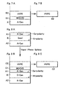
- the layer B) may be composed of at least two layers and the first layer B1) may be prepared on a substrate having the layer A) by means of MOCVD or MBE and the second layer B2) may be prepared on the first layer B1) by means of HVPE as shown in Fig.7A .
- a substrate having a thickness of 100 to 300 ⁇ m or more can be obtained from a portion of the layer B2) in the combination layers of A) the layer of bulk mono-crystal nitride containing at least one element of alkali metals (Group I, IUPAC 1989), B1) the layer of nitride grown by means of MOCVD or MBE and B2) the layer of gallium-containing nitride grown by means of HVPE.
- the resulting template can consist of substantially complete Ga-polar face area at one of sides of the substrate, that is, more than 95%, preferably more than 99 % of Ga-polar face.
- a template type substrate may comprise the layer A) of bulk mono-crystal nitride prepared on a seed having the layer B) by crystallization of nitride in a supercritical ammonium solution containing at least one element of alkali metals.
- the template type substrate may further comprise a layer C) of gallium-containing nitride grown by means of vapor phase epitaxy growth wherein the layer A) of bulk mono-crystal nitride containing at least one element of alkali metals (Group I, IUPAC 1989) is prepared on both of N-polar face and non N-polar face such as Ga-polar face or Al-polar face of the seed layer B) as layers A1) and A2) as shown in Fig.8A and the layer C) is combined at non N-polar face of the layer A2) and N-polar face of the layer C).
- the layer A) of bulk mono-crystal nitride containing at least one element of alkali metals Group I, IUPAC 1989
- the layer C) of the gallium-containing nitride may be prepared on a substrate of the layer A2) by means of MOCVD, HVPE or MBE.
- the layer C) can be composed of at least two layers and the first layer C1) is prepared on a substrate of the layer A2) by means of MOCVD or MBE and the second layer C2) can be prepared on the first layer C1) by means of HVPE as shown in Fig.8B .
- the first layer C1) can protect the surface of the substrate A) not to be interfered by a HVPE process for the layer C2) and also can avoid diffusion of Alkali metals from the substrate A) to the layer C2).
- the layer C1) is preferably prepared at a temperature lower than a formation temperature of mono-crystal thereof.
- a substrate having a thickness of 100 to 300 ⁇ m or more which is sliced off from a portion of the layer C2) in the combination layers of A1) the layer of bulk mono-crystal nitride containing at least one element of alkali metals (Group I, IUPAC 1989), B) the layer of nitride grown by vapor phase epitaxy growth, A2) the layer of bulk mono-crystal nitride containing at least one element of alkali metals (Group I, IUPAC 1989), C1) the layer grwon by means of MOCVD or MBE and C2) the layer of gallium-containing nitride grown by means of HVPE.
- the HVPE substrate contains chloride and has a main surface substantially consisting of Ga-polar face as mentioned above.
- a substrate having a dislocation density of 10 6 /cm 2 or less as well as the value of FWHM of the X-ray rocking curve from (0002) plane less than 80 arcsec, preferably 10 6 /cm 2 or less, more preferably 10 4 /cm 2 or less.
- a template type substrate as shown in Fig.9 wherein the layer A) is a hexagonal shaped substrate having a pair of C-plane surfaces with edge periphery of M-plane having a diameter of 1 inch or more, which is prepared from a substrate made by A-axis direction growth of bulk mono-crystal nitride in a supercritical ammonium solution containing at least one element of alkali metals. It is suprising that the substrate has a dislocation density of 10 4 /cm 2 or less.
- the substrate according to the present invention is characterized in that even if the gallium-containing nitride layer B) or C) and layers B1) and B2) or C1) and C2) contain at least one element of alkali metals, the content is less than that of the layer A) prepared by crystallization of nitride in a supercritical ammonium solution containing at least one element of alkali metals. Because the content of Alkali metals is caused by diffusion from the layer A) during the process of forming layer B) or C) and layers B1) and B2) or C1) and C2). In this case, the layer B), B1), C) or C1) may be prepared by MOCVD and preferably has a thickness of 0.1 to 3 ⁇ m.
- the layer C) obtained by the growth method from the gaseous phase is also represented by the general formula of Al x Ga 1-x-y In y N, where 0 ⁇ x ⁇ 1, 0 ⁇ y ⁇ 1, 0 ⁇ x+y ⁇ 1 as shown in the definition of the layer B). Therefore, in a preferred embodiment of the present invention, the layer B) or C) may be combination of double layers AlGaN and GaN. In case of the first layer B1) or C1) of AlGaN formed at a lower temperature than that of mono-crystal, the second layer B2) or C2) of GaN will be improving in a quality of crystalline.
- the layer B), B2), C) or C2) is a gallium-containing nitride containing silicon (Si) or oxygen (O) as donor dopants or a gallium-containing nitride containing magnesium (Mg) or zinc (Zn) as acceptor dopants because of vapor phase epitaxy growth.
- concentration of dopants preferably ranges between 10 16 /cm 3 and 10 21 /cm 3 .
- a process of preparing a substrate for opto-electric or electrical devices which comprises steps of:
- the step (b) preferably comprises (b1) forming a layer B1) or C1) of nitride by means of vapor phase epitaxy growth on A1 or Ga-polar face of the layer A) and (b2) forming a layer B2) or C2) of nitride by means of vapor phase epitaxy growth on the layer B1) or C1).
- the layer B2) or C2) is sliced off from the substrate A) to get a substrate having a thickness of 100 ⁇ m or more and a main surface substantially consisting of A1 or Ga-polar face.
- a good substrate can make a further good substrate, so that the substrate according to the present invention is used for making a further substrate.
- the process further comprises (d) forming a new layer D) of nitride by means of vapor phase epitaxy growth on A1 or Ga-polar face of the layer B), C), B2) or C2), which will be slicd off from the substrate B), C), B2) or C2) to get a substrate having a thickness of 100 ⁇ m or more and a main surface substantially consisting of A1 or Ga-polar face.
- a further step of (c) polishing one of the faces of the layer B) to get a substrate for vapor phase epitaxy in order to get a good surface property for further epitaxy growth in order to get a substrate having a thickness of 100 ⁇ m or more, preferably 150 ⁇ m or more and a main surface substantially consisting of A1 or Ga-polar face, it is needed to get the layer B), B2), C), C2) or D) having a thickness of 100 ⁇ m or more, preferably 150 ⁇ m or more and slice off one or more portions of the layer B), B2), C), C2) or D).
- the resulting substrate may be subjected to an annealing treatment in an atmosphere that does not contain hydrogen at a temperature between approx. 600 and 1050°C, thus producing material with better crystalline quality than before the annealing.
- the step of annealing is preferably carried out in the atmosphere of inert gas with an addition of oxygen between 10 and 30 vol.% and the step of annealing can be carried out in a single step or in multiple steps until the desired level of impurities (such as hydrogen and/or ammonia or ions formed from the impurities formed during the crystallization and/or annealing process) is reached.
- impurities such as hydrogen and/or ammonia or ions formed from the impurities formed during the crystallization and/or annealing process
- This invention is based on an ammono-basic growth of the crystal and allows to obtain mono-crystalline gallium or aluminum-containing nitride selectively deposited on the seed's surface by way of creating chemical transport in a supercritical ammonia-containing solvent containing one or more mineralizers affecting its ammono-basic nature.
- This process is characterized in that it allows to obtain bulk mono-crystalline template-type substrate with a layer of high structural quality, in which on the gallium or aluminum-containing nitride layer obtained by the growth method from the gaseous phase a gallium or aluminum-containing nitride layer was deposited thanks to the fact that in the autoclave a supercritical ammonia-containing solution and alkali metal ions are created.
- the feedstock is dissolved, followed by selective crystallization of the gallium or aluminum-containing nitride from the solution on the seed surface at a higher temperature and/or lower pressure than that of the process of dissolving the feedstock containing gallium in the supercritical solvent.
- the second embodiment of this invention concerns the process of crystallization of the bulk mono-crystalline gallium or aluminum-containing nitride, characterized in that it allows to obtain a bulk mono-crystalline template-type substrate with a high structural quality layer, in which on the gallium or aluminum-containing nitride layer obtained by the growth method from the gaseous phase, a gallium or aluminum-containing nitride layer with high structural quality was deposited, and consists in conducting a dissolution in supercritical ammonia-containing solution and alkali metal ions, creating supercritical solution with a negative temperature coefficient of gallium nitride solubility and, at least in the autoclave zone in which the seed was placed, creating a zone where supercritical solution is supersaturated with respect to the seed, and regulating the concentration by appropriately increasing the temperature and/or lowering the pressure in order to ensure that no spontaneous crystallization can occur, and achieve a
- the dissolution zone and the crystallization zone it is advisable to control the supersaturation of the supercritical solution with respect to the seed by regulating the temperature of dissolution and the temperature of crystallization. Moreover, temperature management would be facilitated if the temperature in the crystallization zone is set between 300 and o 600°C, and the difference between the temperature in the dissolution zone and the crystallization zone in the autoclave is maintained below 150°C, preferably under 100°C.
- the supersaturation of the supercritical solution with respect to the seed can be regulated by placing one or more baffles in the autoclave to separate the dissolution zone (with low temperature) from the crystallization zone (with high temperature) and controlling the rate of the convection flow between those zones. Moreover, if the two zones are created in the autoclave: the dissolution zone and the crystallization zone, with an appropriate difference in temperature, the supersaturation of the supercritical solution with respect to the seed can be regulated by using the gallium or aluminum-containing feedstock, introduced in the form of crystalline GaN, whose total surface exceeds the total surface of the seed.
- ions of alkali metals are introduced in the form of alkali metals and/or alkali metal compounds and/or their mixtures, particularly those not containing elements of Group XVII (halogens).
- Such ions of alkali metals may include one or more types selected from Li + , Na + , and K + . It is preferable to apply them in the form of alkali metals and their amides and azides in the molar ratio to ammonia between 1:200 and 1:2.
- the feedstock dissolved in the supercritical solution is gallium or aluminum-containing nitride or a gallium precursor, which may form gallium compounds soluble in the supercritical solvent.
- the feedstock can be gallium or aluminum-containing nitride which undergoes a reversible process of dissolution in the supercritical ammonia-containing solvent. It can be also merged with metallic gallium which undergoes an irreversible reaction in the supercritical solvent.
- gallium or aluminum-containing nitride in the form of gallium nitride facilitates the control over the crystallization process.
- the seeds of mono-crystalline GaN although the following can also be used: GaN obtained through the HVPE method or the flux method, the seeds obtained through the high-pressure method, the seeds with A (11 2 0), M (1 1 00), or R (1 1 02) surfaces cut out from the bulk mono-crystal obtained from supercritical ammono method.
- the C (0001) surface having N-polarity For the purposes of the crystallization it is also possible to use the C (0001) surface having N-polarity.
- the processes of dissolution and crystallization are usually carried out at in parallel, and they are concurrently spatially separated in the autoclave.
- the supercritical ammonia-containing solvent is obtained in the autoclave, which contains ions of alkali metals.
- This solvent dissolves the gallium or aluminum-containing feedstock, and crystallization of gallium or aluminum-containing nitride is carried out from the supercritical solution on the surface of seed in the conditions of a higher temperature and/or lower pressure than that for the process of dissolution of the feedstock.
- the process of dissolving the gallium or aluminum-containing feedstock be supplemented with a separate process of transferring the supercritical solution to a place with higher temperature and/or lower pressure.
- the gallium or aluminum-containing feedstock is placed in the dissolution zone with low temperature while the seed is placed in the crystallization zone with high temperature.
- the difference in temperature between the dissolution zone and the crystallization zone should be set in such a way as to ensure chemical transport through the supercritical solution, which occurs mainly through the process of convection.
- the difference in temperature between the dissolution zone and the crystallization zone exceeds 1°C, preferably between 5 and 150°C, and most preferably below 100°C.
- the nitride obtained in this invention has the formula of Al x Ga 1-x-y In y N, where 0 ⁇ x ⁇ 1, 0 ⁇ y ⁇ 1, 0 ⁇ x+y ⁇ 1.
- the supercritical solvent is defined as follows: it contains NH 3 and/or its derivatives and a mineralizer in the form of alkali metal ions, or at least sodium or potassium ions.
- the feedstock consists primarily of gallium or aluminum-containing nitride or its precursors selected out of the group including: azides, imides, amido-imides, amides, hydrides, gallium or aluminum-containing metallic compounds and alloys, as well as metallic gallium. The definition of a precursor can be found further in this document.
- the seed contains at least a crystalline layer of gallium or aluminum-containing nitride or other elements of Group XIII (IUPAC 1989). It is preferable that the surface dislocation density of that layer be lower than 10 6 /cm 2 .
- crystallization of gallium or aluminum-containing nitride can occur in the temperature between 100 and 800°C, preferably between 300 and 600°C, and most preferably between 400 and 550°C.
- the pressure can range between 10 and 1000 MPa, preferably between 100 and 550MPa, and most preferably between 150 and 300MPa.
- the concentration of alkali metal ions in the supercritical solvent is regulated in such a way as to ensure proper solubility properties of the feedstock and the gallium or aluminum-containing nitride, and the molar ratio of alkali metal ions to other species in the supercritical solvent is controlled in the range from 1:200 to 1:2, preferably between 1:100 and 1:5, and most preferably between 1:20 and 1:8.
- the growth of a mono-crystalline gallium or aluminum-containing nitride is obtained by chemical transport in the supercritical solvent containing one or more mineralizers affecting its ammono-basic nature.
- this is the technique of ammono-basic crystallization, and the terms used in this invention should be understood in accordance with the following definitions:
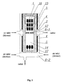
- the dissolution zone 13 of a 600cm 3 high pressure autoclave 1 having the inner diameter of 40mm and length of 480mm, was charged with 53.0g of feedstock in the form of metallic gallium (6N).
- the crystallization zone 14 of the same autoclave was charged with a seed crystal in the form of a gallium nitride wafer (having the diameter of about 1 inch and the mass of 2.0g) obtained by means of A-axis direction growth in the supercritical ammono method as shown in Fig.9 .
- the seed is made of the wafer having a length (L), an A-axis direction growth (W) from both sides of A-plane and edge periphery of M-planes)
- the temperature of the dissolution zone was increased to 500°C (at 1°C/min), the temperature of the crystallization zone was slowly increased to 550°C (at 0.1°C/min, Fig. 6 ), with the pressure inside the autoclave reaching about 280MPa.
- the autoclave was kept under those conditions (the second step of the process) for the subsequent 20 days ( Fig.6 ).
- partial dissolution of the feedstock i.e. polycrystalline GaN
- crystallization of gallium nitride on the HVPE seed took place in the crystallization zone.
- the gallium nitride crystallized on both sides of the seed in the form of mono-crystalline layers with the total thickness of about 2mm.
- the step of removing impurities from bulk mono-crystalline nitride by a process of rinsing in the environment of supercritical ammonia-containing solvent, water or carbon dioxide or being subjected to the action of gaseous hydrogen, nitrogen or ammonia.
- the step of rinsing may be carried out with aid of the application of ultrasounds or the exposure to an electron beam.
- the resulting template type substrate is very useful for the epitaxy substrate from gaseous phase such as MOCVD, MBE and HVPE, resulting in possibility of making good opto-electric devices such as Laser Diode and large-output LED and good electric devices such as MOSFET.
Abstract
Description
- This invention is related to a substrate for epitaxy used to make opto-electric devices such as LED and LD or electric devices such as MOSFET.
- The currently used substrates for a vapor phase epitaxy typically include Sapphire, SiC, GaAs and Si and the resulting epitaxy layers grown on the substrate have been still in the unfavorably high dislocation density of 109/cm2. Therefore, there have been proposed an application of ELOG-type structures to the substrate, which allows to decrease the dislocation density down to 106/cm2, but that density is still too high to ensure the correct functioning of many electronic and opto-electronic devices, particularly high power semiconductor lasers. Further, there is another problem that the resulting substrates have a decreased epitaxy face area because of the ELOG structure. Accordingly, we have proposed the other processes for obtaining mono-crystalline gallium-containing nitrides, For example, Polish patent application No.
P-347918 - 1) The inventors of this invention have further discovered from their sharp researches that it is possible to significantly lower the dislocation density of the gaseous or vapor phase epitaxy layer without the ELOG structure if such a gaseous phase growth process is carried out on the surface of a substrate of bulk mono-crystalline gallium-containing nitride made by means of crystallization from supercritical ammonia-containing solution, and also to keep all the main surface of the substrate as the complete Ga-polar face for further epitaxy process of making opto-electric or electric devices. This is quite different from the ELOG-type substrate.
- Furthermore, 2) the inventors have discovered that A-axis direction growth of GaN is 4 times or more faster than that of C-axis direction in a supercritical ammono method containing at least one alkali metals and get a mono-crystal nitride substrate having a diameter of 25,4 mm (1 inch) or more provided with a good quality such as C-axis orientation perpendicular to the C-plane extending at least 30µm, preferably 50µm or more. This is also quite different from the ELOG-type substrate.
- According to the above findings 1) and 2) of the inventors, if an GaN layer is grown by means of HVPE on a mono-crystal nitride substrate made by the supercritical ammono method to have a thickness of 100 µm or more, preferably 150 µm or more and is sliced off from the mono-crystal nitride substrate, the resulting HVPE GaN have a dislocation density of 5×10⁵/cm2 or less, preferably of 105/cm2, more preferably 104/cm2 or less and one of the surface substantially consists of Ga-polar face and is better than any ELOG GaN substrate.
- Therefore, the object of this invention is to provide a substrate for epitaxy as set forth in
claim 1 and a method as set forth inclaim 3 of preparing a substrate based on the new bulk mono-crystal of nitride. - According to a first aspect of the present invention, there is provided a substrate used for opto-electric or electrical devices which comprises a layer of nitride grown by means of vapor phase epitaxy growth wherein both main surfaces of the nitride substrate are substantially consisting of non N-polar face and N-polar face respectively and the dislocation density of the substrate is 5×10⁵/cm2 or less.
- According to the present invention, we can get an excellent vapor epitaxy layer grown on Ga or Al-polar face of a mono-crystal substrate of AlxGa1-xN wherein 0≤x≤1 if the substrate can be prepared by means of a method of using a supercritical ammono solution and the resulting substrate comprising the layer B) is very useful for making opto-electric or electrical devices by the vapor phase epitaxy growth.
- The characteristic of the substrate according to the present invention, is in that there is substantially no tilting which means substantially no inclination of C-axis of nitride mono-crystal and also there is substantially no twisting of crystal which means substantially no twist of lattice of mono-crystal. Therefore, our substrate has not such distortion, so that polarization light can pass through the crystal like sapphire, which is quite different from HVPE GaN substrate..
- In the present invention, the layer A) of bulk mono-crystal nitride includes gallium-containing nitride and aluminum-containing nitride and is represented by the general formula of AlxGa1-xN wherein 0≤x≤1. The layer A) is normally provided as an AlN or GaN mono-crystalline substrate which can be made by supercritical ammono methods described in
WO02/101120 WO02/101124 FR 2796657 - In the present invention, the layer B) of nitride grown by means of vapor phase epitaxy growth is represented by the general formula of AlxGa1-x-yInyN, where 0≤x≤1, 0≤y<1, 0≤x+y≤1. The layer B) can be made on a substrate having the layer A) by means of MOCVD(Metal Organic Chemical Vapor Epitaxy), HVPE(Hydride or Halide Vapor Phase Epitaxy) or MBE (Molecular Beam Epitaxy) which methods are well-known to public and the layer B) includes GaN, AlGaN, InGaN and AlGaInN compound semiconductor layers.
- In a preferred embodiment of the present invention, the layer B) may be composed of at least two layers and the first layer B1) may be prepared on a substrate having the layer A) by means of MOCVD or MBE and the second layer B2) may be prepared on the first layer B1) by means of HVPE as shown in
Fig.7A . - According to the present invention, as shown in
Fig.7B , a substrate having a thickness of 100 to 300µm or more can be obtained from a portion of the layer B2) in the combination layers of A) the layer of bulk mono-crystal nitride containing at least one element of alkali metals (Group I, IUPAC 1989), B1) the layer of nitride grown by means of MOCVD or MBE and B2) the layer of gallium-containing nitride grown by means of HVPE. The resulting template can consist of substantially complete Ga-polar face area at one of sides of the substrate, that is, more than 95%, preferably more than 99 % of Ga-polar face. In comparison with HVPE GaN substrate made by the ELOG method having less than 90 % of Ga-polar face area because of some of N-polar face area on the same surface, there is obtained a substrate having an excellent quality as to the dislocation density and FWHM of the X-ray rocking curve as well as the complete Ga-polar face. - According to a second aspect of the present invention, a template type substrate may comprise the layer A) of bulk mono-crystal nitride prepared on a seed having the layer B) by crystallization of nitride in a supercritical ammonium solution containing at least one element of alkali metals. In this case, the template type substrate may further comprise a layer C) of gallium-containing nitride grown by means of vapor phase epitaxy growth wherein the layer A) of bulk mono-crystal nitride containing at least one element of alkali metals (Group I, IUPAC 1989) is prepared on both of N-polar face and non N-polar face such as Ga-polar face or Al-polar face of the seed layer B) as layers A1) and A2) as shown in
Fig.8A and the layer C) is combined at non N-polar face of the layer A2) and N-polar face of the layer C). Therefore, the layer C) of the gallium-containing nitride may be prepared on a substrate of the layer A2) by means of MOCVD, HVPE or MBE. In a preferred embodiment, the layer C) can be composed of at least two layers and the first layer C1) is prepared on a substrate of the layer A2) by means of MOCVD or MBE and the second layer C2) can be prepared on the first layer C1) by means of HVPE as shown inFig.8B . According to this invention, the first layer C1) can protect the surface of the substrate A) not to be interfered by a HVPE process for the layer C2) and also can avoid diffusion of Alkali metals from the substrate A) to the layer C2). The layer C1) is preferably prepared at a temperature lower than a formation temperature of mono-crystal thereof. - In this case, as shown in
Fig.8C , there can be obtained a substrate having a thickness of 100 to 300µm or more which is sliced off from a portion of the layer C2) in the combination layers of A1) the layer of bulk mono-crystal nitride containing at least one element of alkali metals (Group I, IUPAC 1989), B) the layer of nitride grown by vapor phase epitaxy growth, A2) the layer of bulk mono-crystal nitride containing at least one element of alkali metals (Group I, IUPAC 1989), C1) the layer grwon by means of MOCVD or MBE and C2) the layer of gallium-containing nitride grown by means of HVPE. The HVPE substrate contains chloride and has a main surface substantially consisting of Ga-polar face as mentioned above. - According to this invention, there can be obtained a substrate having a dislocation density of 106/cm2 or less as well as the value of FWHM of the X-ray rocking curve from (0002) plane less than 80 arcsec, preferably 106/cm2 or less, more preferably 104/cm2 or less.
- In the supercritical ammono process, we have discovered that A-axis growth is faster 4 times or more than that of C-axis growth and A-axis growth in the supercritical ammono method makes a dislocation density decreased too much in comparison with C-axis growth in the same supercritical ammono method. Therefore, according to the new aspect of the invention, we can get a template type substrate as shown in
Fig.9 wherein the layer A) is a hexagonal shaped substrate having a pair of C-plane surfaces with edge periphery of M-plane having a diameter of 1 inch or more, which is prepared from a substrate made by A-axis direction growth of bulk mono-crystal nitride in a supercritical ammonium solution containing at least one element of alkali metals. It is suprising that the substrate has a dislocation density of 104/cm2 or less. - The substrate according to the present invention is characterized in that even if the gallium-containing nitride layer B) or C) and layers B1) and B2) or C1) and C2) contain at least one element of alkali metals, the content is less than that of the layer A) prepared by crystallization of nitride in a supercritical ammonium solution containing at least one element of alkali metals. Because the content of Alkali metals is caused by diffusion from the layer A) during the process of forming layer B) or C) and layers B1) and B2) or C1) and C2). In this case, the layer B), B1), C) or C1) may be prepared by MOCVD and preferably has a thickness of 0.1 to 3 µm.
- In case of the substrate according to the present invention, the layer C) obtained by the growth method from the gaseous phase is also represented by the general formula of AlxGa1-x-yInyN, where 0≤x≤1, 0≤y<1, 0≤x+y≤1 as shown in the definition of the layer B). Therefore, in a preferred embodiment of the present invention, the layer B) or C) may be combination of double layers AlGaN and GaN. In case of the first layer B1) or C1) of AlGaN formed at a lower temperature than that of mono-crystal, the second layer B2) or C2) of GaN will be improving in a quality of crystalline.
- In case of the template type substrate according to the present invention, the layer B), B2), C) or C2) is a gallium-containing nitride containing silicon (Si) or oxygen (O) as donor dopants or a gallium-containing nitride containing magnesium (Mg) or zinc (Zn) as acceptor dopants because of vapor phase epitaxy growth. The concentration of dopants preferably ranges between 1016/cm3 and 1021/cm3.
- According to a third aspect of the present invention, there is provided a process of preparing a substrate for opto-electric or electrical devices which comprises steps of:
- (a) preparing a layer A) of bulk mono-crystal nitride containing at least one element of alkali metals (Group I, IUPAC 1989) to have a thichness for substrate by crystallization of gallium or aluminum-containing nitride on a seed from a super-critical ammonia-containing solution; (b) forming a layer B) or C) of nitride by means of vapor phase epitaxy growth on Al or Ga-polar face of the layer A);
- and (c) slicing the layer B) or C) off from the substrate A) to get a substrate having a thickness of 100 µm or more and a main surface substantially consisting of A1 or Ga-polar face.
- As shown in
Figs.7A and 7B and Figs.8A to 8C , in a preferred process of preparing a substrate for opto-electric or electrical devices, the step (b) preferably comprises (b1) forming a layer B1) or C1) of nitride by means of vapor phase epitaxy growth on A1 or Ga-polar face of the layer A) and (b2) forming a layer B2) or C2) of nitride by means of vapor phase epitaxy growth on the layer B1) or C1). In this case, the layer B2) or C2) is sliced off from the substrate A) to get a substrate having a thickness of 100 µm or more and a main surface substantially consisting of A1 or Ga-polar face. - According to a fourth aspect of the present invention, a good substrate can make a further good substrate, so that the substrate according to the present invention is used for making a further substrate. In this case, the process further comprises (d) forming a new layer D) of nitride by means of vapor phase epitaxy growth on A1 or Ga-polar face of the layer B), C), B2) or C2), which will be slicd off from the substrate B), C), B2) or C2) to get a substrate having a thickness of 100 µm or more and a main surface substantially consisting of A1 or Ga-polar face.
- In a preferred embodiment of the present invention, it may be needed a further step of (c) polishing one of the faces of the layer B) to get a substrate for vapor phase epitaxy in order to get a good surface property for further epitaxy growth. Further, in order to get a substrate having a thickness of 100 µm or more, preferably 150µm or more and a main surface substantially consisting of A1 or Ga-polar face, it is needed to get the layer B), B2), C), C2) or D) having a thickness of 100µm or more, preferably 150µm or more and slice off one or more portions of the layer B), B2), C), C2) or D).
- The resulting substrate may be subjected to an annealing treatment in an atmosphere that does not contain hydrogen at a temperature between approx. 600 and 1050°C, thus producing material with better crystalline quality than before the annealing. The step of annealing is preferably carried out in the atmosphere of inert gas with an addition of oxygen between 10 and 30 vol.% and the step of annealing can be carried out in a single step or in multiple steps until the desired level of impurities (such as hydrogen and/or ammonia or ions formed from the impurities formed during the crystallization and/or annealing process) is reached.
- Further, it is sometimes needed to remove impurities from bulk mono-crystalline nitride by a process of rinsing in the environment of supercritical ammonia-containing solvent, water or carbon dioxide or being subjected to the action of gaseous hydrogen, nitrogen or ammonia. In this case, it is preferable to carry out the step of rinsing with aid of the application of ultrasounds or the exposure to an electron beam.
- The invention is illustrated in the enclosed figures:
-
Fig.1 is a graph showing the change in time of the temperature in the autoclave where p=const and shows the relation between the changes in the temperature and the dissolution and crystallization processes in the case of this invention; -
Fig.2 is a graph showing the change in time of the pressure in the autoclave where T=const and illustrates the relation between the changes in the pressure and the processes of dissolution and crystallization in the case of this invention; -
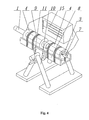
Fig.3 is a vertical sectional view of the autoclave and the set of furnaces used for carrying out this invention; -
Fig.4 is a perspective view of the apparatus used for obtaining bulk mono-crystalline gallium nitride; -
Fig.5 is a graph showing the relationship between the solubility of GaN in the supercritical ammonia which contains potassium amides (with Mineralizer: NH3=0.07) and the pressure, where T=400°C and T=500°C; finally, -
Fig.6 is a graph showing the change in time of the temperature in the autoclave for the purposes of this Example. -
Fig.7A and 7B are schematic sectional views of the first embodiment of the template type substrate according to the present invention. -
Fig.8A, 8B and 8C are schematic sectional views of the second embodiment of the template type substrate according to the present invention. -
Fig.9 is a schematic plane view showing a process of making A-axis direction growth seed. - This invention is based on an ammono-basic growth of the crystal and allows to obtain mono-crystalline gallium or aluminum-containing nitride selectively deposited on the seed's surface by way of creating chemical transport in a supercritical ammonia-containing solvent containing one or more mineralizers affecting its ammono-basic nature.
- This process is characterized in that it allows to obtain bulk mono-crystalline template-type substrate with a layer of high structural quality, in which on the gallium or aluminum-containing nitride layer obtained by the growth method from the gaseous phase a gallium or aluminum-containing nitride layer was deposited thanks to the fact that in the autoclave a supercritical ammonia-containing solution and alkali metal ions are created. In the autoclave the feedstock is dissolved, followed by selective crystallization of the gallium or aluminum-containing nitride from the solution on the seed surface at a higher temperature and/or lower pressure than that of the process of dissolving the feedstock containing gallium in the supercritical solvent.
- The objective of the first embodiment is to perform a selective crystallization on the seed surface during the second process - crystallization. Therefore, the second embodiment of this invention concerns the process of crystallization of the bulk mono-crystalline gallium or aluminum-containing nitride, characterized in that it allows to obtain a bulk mono-crystalline template-type substrate with a high structural quality layer, in which on the gallium or aluminum-containing nitride layer obtained by the growth method from the gaseous phase, a gallium or aluminum-containing nitride layer with high structural quality was deposited, and consists in conducting a dissolution in supercritical ammonia-containing solution and alkali metal ions, creating supercritical solution with a negative temperature coefficient of gallium nitride solubility and, at least in the autoclave zone in which the seed was placed, creating a zone where supercritical solution is supersaturated with respect to the seed, and regulating the concentration by appropriately increasing the temperature and/or lowering the pressure in order to ensure that no spontaneous crystallization can occur, and achieve a selective growth of the gallium or aluminum-containing nitride crystal solely on the surface of the seed placed in the autoclave.
- Although in the second embodiment two zones are created simultaneously in the autoclave: the dissolution zone and the crystallization zone, it is advisable to control the supersaturation of the supercritical solution with respect to the seed by regulating the temperature of dissolution and the temperature of crystallization. Moreover, temperature management would be facilitated if the temperature in the crystallization zone is set between 300 and o 600°C, and the difference between the temperature in the dissolution zone and the crystallization zone in the autoclave is maintained below 150°C, preferably under 100°C. The supersaturation of the supercritical solution with respect to the seed can be regulated by placing one or more baffles in the autoclave to separate the dissolution zone (with low temperature) from the crystallization zone (with high temperature) and controlling the rate of the convection flow between those zones. Moreover, if the two zones are created in the autoclave: the dissolution zone and the crystallization zone, with an appropriate difference in temperature, the supersaturation of the supercritical solution with respect to the seed can be regulated by using the gallium or aluminum-containing feedstock, introduced in the form of crystalline GaN, whose total surface exceeds the total surface of the seed.
- In the first embodiment ions of alkali metals are introduced in the form of alkali metals and/or alkali metal compounds and/or their mixtures, particularly those not containing elements of Group XVII (halogens). Such ions of alkali metals may include one or more types selected from Li+, Na+, and K+. It is preferable to apply them in the form of alkali metals and their amides and azides in the molar ratio to ammonia between 1:200 and 1:2. The feedstock dissolved in the supercritical solution is gallium or aluminum-containing nitride or a gallium precursor, which may form gallium compounds soluble in the supercritical solvent.
- Although the process described in this invention is based on the reactions in a clear ammono-basic environment, application of feedstock in the form of GaN obtained by the HVPE method or another chemical method is also allowed, provided that chlorine or other elements of Group XVII do not negatively affect the environment in which the reaction occurs.
- The feedstock can be gallium or aluminum-containing nitride which undergoes a reversible process of dissolution in the supercritical ammonia-containing solvent. It can be also merged with metallic gallium which undergoes an irreversible reaction in the supercritical solvent.
The use of gallium or aluminum-containing nitride in the form of gallium nitride facilitates the control over the crystallization process. It is preferable to use the seeds of mono-crystalline GaN, although the following can also be used: GaN obtained through the HVPE method or the flux method, the seeds obtained through the high-pressure method, the seeds with A (112 0), M (11 00), or R (11 02) surfaces cut out from the bulk mono-crystal obtained from supercritical ammono method. For the purposes of the crystallization it is also possible to use the C (0001) surface having N-polarity. - In this invention, the processes of dissolution and crystallization are usually carried out at in parallel, and they are concurrently spatially separated in the autoclave. In other words, the supercritical ammonia-containing solvent is obtained in the autoclave, which contains ions of alkali metals. This solvent dissolves the gallium or aluminum-containing feedstock, and crystallization of gallium or aluminum-containing nitride is carried out from the supercritical solution on the surface of seed in the conditions of a higher temperature and/or lower pressure than that for the process of dissolution of the feedstock.
- In the first embodiment it is recommended that the process of dissolving the gallium or aluminum-containing feedstock be supplemented with a separate process of transferring the supercritical solution to a place with higher temperature and/or lower pressure. In this case, in the autoclave at least two zones are formed with different temperature, and the gallium or aluminum-containing feedstock is placed in the dissolution zone with low temperature while the seed is placed in the crystallization zone with high temperature. The difference in temperature between the dissolution zone and the crystallization zone should be set in such a way as to ensure chemical transport through the supercritical solution, which occurs mainly through the process of convection. The difference in temperature between the dissolution zone and the crystallization zone exceeds 1°C, preferably between 5 and 150°C, and most preferably below 100°C.
Preferably, the nitride obtained in this invention has the formula of AlxGa1-x-yInyN, where 0≤x≤1, 0≤y<1, 0≤x+y≤1. The supercritical solvent is defined as follows: it contains NH3 and/or its derivatives and a mineralizer in the form of alkali metal ions, or at least sodium or potassium ions. The feedstock consists primarily of gallium or aluminum-containing nitride or its precursors selected out of the group including: azides, imides, amido-imides, amides, hydrides, gallium or aluminum-containing metallic compounds and alloys, as well as metallic gallium. The definition of a precursor can be found further in this document.
In this invention, the seed contains at least a crystalline layer of gallium or aluminum-containing nitride or other elements of Group XIII (IUPAC 1989). It is preferable that the surface dislocation density of that layer be lower than 106/cm2 .
In this invention, crystallization of gallium or aluminum-containing nitride can occur in the temperature between 100 and 800°C, preferably between 300 and 600°C, and most preferably between 400 and 550°C. During crystallization of the gallium or aluminum-containing nitride the pressure can range between 10 and 1000 MPa, preferably between 100 and 550MPa, and most preferably between 150 and 300MPa.
The concentration of alkali metal ions in the supercritical solvent is regulated in such a way as to ensure proper solubility properties of the feedstock and the gallium or aluminum-containing nitride, and the molar ratio of alkali metal ions to other species in the supercritical solvent is controlled in the range from 1:200 to 1:2, preferably between 1:100 and 1:5, and most preferably between 1:20 and 1:8.
In this invention, the growth of a mono-crystalline gallium or aluminum-containing nitride is obtained by chemical transport in the supercritical solvent containing one or more mineralizers affecting its ammono-basic nature. Thus, this is the technique of ammono-basic crystallization, and the terms used in this invention should be understood in accordance with the following definitions: - Group XIII element(s) nitride means a nitride of Group XIII element(s), i.e. aluminum, gallium and indium either alone or in any combination. Gallium-containing nitride is the most preferred such nitride.
- Gallium- or aluminum-containing nitride means a nitride of gallium (or: aluminum) and optionally other element(s) of Group XIII (according to IUPAC, 1989). It includes, but is not restricted to, the binary compound - GaN (or A1N), a ternary compound - AlGaN, InGaN or a quaternary compound AlInGaN, preferably containing a substantial portion of gallium, anyhow at the level higher than dopant content. The composition of other elements with respect to gallium (aluminum) may be modified in its structure insofar as it does not collide with the ammono-basic nature of the crystallization technique. (The mentioned formulas are only intended to give the components of the nitrides. They are not intended to indicate their relative amounts.)
- Bulk mono-crystal of gallium- or aluminum-containing nitride means a mono-crystalline substrate in the form of gallium or aluminum-containing nitride, on which opto-electronic devices may be obtained, such as: light-emitting diodes (LED) or laser diodes (LD) by the MOCVD-method or by the methods of epitaxy growth such as the HVPE method.
- C-, A- or M-plane refers to C-, A- or M-plane surfaces of hexagonal Group XIII element nitride crystals.
- Precursor of gallium- or aluminum-containing nitride is a substance or a mixture containing at least gallium (aluminum), which may also contain alkali metals, elements of Group XIII (according to IUPAC 1989), nitrogen and/or hydrogen, and metallic gallium, its alloys or metallic compounds, hydrides, amides, imides, amido-imides and azides, which may form gallium compounds soluble in the supercritical ammonia-containing solvent as defined below.
- Gallium- or aluminum-containing feedstock is gallium- or aluminum-containing nitride or its precursor. Feedstock can be in the form of: GaN (AlN) obtained by any method, e.g. flux methods, HNP method, HVPE method, or polycrystalline GaN (AlN) obtained in situ from metallic gallium (aluminum) as the result of a chemical reaction in the supercritical ammonia-containing solvent.
- Supercritical ammonia-containing solvent is a supercritical solvent consisting at least of ammonia, which contains one or more types of ions of alkali metals, used for dissolution of gallium- or aluminum-containing feedstock. The supercritical ammonia-containing solvent may also contain derivatives of ammonia and/or their mixtures, in particular - hydrazine.
- Mineralizer is a substance delivering one or more types of ions of alkali metals to the supercritical ammonia-containing solvent, supporting dissolution of gallium- or aluminum-containing nitride.
- Substances containing oxygen-free species causing the weakening of ammono-basic nature of the supercritical solution are selected from the group which includes:
- a) compounds AmBn, where A means H+ and/or metal, preferably alkali, NH4 +, Si, S, P, whereas B means halogens, S, P, and n and m mean corresponding stoichiometric coefficients not lower than 1 and/or
- b) groups of species such as:
- S4N4, S2N2, SN, S4N2, S11N2, P3N5, P4N6, PN,
- PN2 - 1 PN3 4-, PN4 7-, PN-, PN2-,
- PNCl2, P(NH)2NH2, P4S10, NP (SNH4)2, NPSNH4SH, NP(SH)2, PNS, Sulfur or silicon species built in the crystalline lattice of the gallium-containing nitride serve as donors; magnesium, zinc or cadmium are acceptors; dopants such as manganese or chromium in the crystalline gallium nitride lattice provide it with magnetic properties; whereas phosphor atoms are isoelectronic with respect to nitrogen atoms, and thus they make the energy gap narrower than that in the pure gallium-containing nitride. Those species do not only cause the weakening of ammono-basic nature of the supercritical solvent, but they also modify optical, electrical and magnetic properties of the gallium-containing nitride.
- Dissolution of the gallium-containing feedstock is a reversible or irreversible process of formation, through the feedstock, of gallium compounds soluble in the supercritical solvent, for example gallium complexes. Gallium complexes are chemical complex compounds, in which centrally placed gallium atom is surrounded by NH3-type ligands or their derivatives, such as NH2-, NH2-. Analogical definition for dissolution of the aluminum-containing feedstock applies.
- Supercritical ammonia-containing solution means a solution obtained as a result of dissolution of the gallium- or aluminum-containing feedstock in the supercritical ammonia-containing solvent.
- Solubility: Our experiences show that equilibrium may be achieved between the solid, which is gallium- or aluminum-containing nitride, and the supercritical solution at sufficiently high temperature and pressure. Therefore, solubility of gallium- or aluminum-containing nitride may be defined as the equilibrium concentration of soluble gallium (aluminum) compounds obtained in the above mentioned process of dissolution of gallium- or aluminum-containing nitride. In this process, the equilibrium concentration, i.e. solubility, may be controlled by modifying the composition of the solvent, temperature and/or pressure.
- Negative temperature coefficient of solubility (negative TCS) means that the solubility of the respective compound is a monotonically decreasing function of temperature if all the other parameters are kept constant. Similarly,positive pressure coefficient of solubility (positive PCS) means that, if all the other parameters are kept constant, the solubility is a monotonically increasing function of pressure. In our research we have shown that the solubility of gallium- or aluminum-containing nitride in supercritical ammonia-containing solvent possesses a negative temperature coefficient and a positive pressure coefficient in temperature ranging at least from 300°C to 550°C and pressure from 100 to 550 MPa. This means that in accordance to
Fig. 1 , after dissolution of feedstock in an autoclave kept for 8 days at thetemperature 400°C (i.e. after dissolution step) re-crystallization of gallium nitride may be achieved by increasing the temperature inside the autoclave to 500°C, while keeping constant pressure of 200 MPa (crystallization step). On the other hand, as shown inFig. 2 , after dissolution of a feedstock at increased pressure in an autoclave kept for 2 days at the level of 350 MPa (i.e. after dissolution step), re-crystallization of gallium nitride is achieved by means of reducing the pressure to 200 MPa while keeping constant temperature of 500°C (crystallization step). - Supersaturation: If concentration of soluble gallium (aluminum) compounds in the supercritical ammonia-containing solution is higher than solubility of gallium- or aluminum-containing nitride in specific physico-chemical conditions, then the supersaturation of the supercritical ammonia-containing solution with respect to gallium- or aluminum-containing nitride in those conditions can be defined as the difference between the actual concentration and the solubility. While dissolving gallium- or aluminum-containing nitride in a closed system it is possible to obtain the supersaturation state, for example, by increasing temperature or decreasing pressure.
- Chemical transport of gallium- or aluminum-containing nitride in the supercritical ammonia-containing solution is a continuous process involving dissolution in the supercritical solution of the gallium- or aluminum-containing feedstock, transport of soluble gallium compounds through the supercritical solution, as well as crystallization of the gallium- or aluminum-containing nitride from the supersaturated supercritical solution. Generally, the chemical transport can be caused by the difference in temperature, difference in pressure, difference in concentration, or other chemical or physical differences between the feedstock being dissolved and the crystallization product. Due to the process according to the invention, it is possible to obtain bulk mono-crystalline gallium- or aluminum-containing nitride as a result of the chemical transport in the conditions of temperature difference, yet it is necessary to maintain higher temperature in the crystallization zone than in the dissolution zone. According to the invention, the chemical transport is preferably caused by convection.
- Seed as it has already been mentioned, is crucial for obtaining desired bulk gallium- or aluminum-containing nitride mono-crystals in a process according to the present invention. In view of the fact that the quality of the seed is crucial for the crystalline quality of the bulk gallium- or aluminum-containing nitride mono-crystals obtained by the process according to the present invention, the seed selected for the process should have possibly high quality. Various structures or wafers having a modified surface can also be used. For example a structure having a number of surfaces spaced adequately far from each other, arranged on a primary substrate and susceptible to the lateral overgrowth of crystalline nitrides may be used as a seed. Moreover, a seed having a homoepitaxial surface, exhibiting n-type electrical conductivity, for example doped with Si, may be used. Such seeds can be produced using processes for gallium-containing nitride crystal growth from gaseous phase, such as HVPE or MOCVD, or else MBE. Doping with Si during the growth process at the level of 1016 to 1021/cm3 ensures n-type electric conductivity. Moreover, a composite seed may be used and in such seed directly on a primary substrate or on a buffer layer made for example of A1N - a layer made of GaN doped with Si may be deposited. Furthermore, for a particular future use, bulk mono-crystals can be grown by the process according to the present invention on homo-seeds having a defined orientation with respect to hexagonal wurzite type crystallographic lattice of the specific Group XIII element(s) nitride, such as C-plane, A-plane or M-plane of the respective nitride.
- Spontaneous crystallization from the supersaturated supercritical ammonia-containing solution means any undesirable process of nucleation and growth of the gallium- or aluminum-containing nitride crystals taking place at any site within the autoclave except on the surface of the seed. The definition also includes growth on the surface of the seed, in which the grown crystal has the orientation different from that of the seed.
- Selective crystallization on the seed means the process of crystallization taking place on the surface of the seed in the absence of spontaneous crystallization, but also when spontaneous crystallization occurs in negligible degree. This process is indispensable to obtain bulk mono-crystal and, at the same time, it is one of the elements of this invention.
- Temperature and pressure of the reaction: In the examples presented in the specification, temperature profile inside the autoclave was measured with use of an empty autoclave, thus without supercritical ammonia-containing solution. Therefore, these are not real temperatures of the process carried out in supercritical conditions. Pressure was measured directly or calculated on the basis of physico-chemical data of ammonia-containing solvent for the assumed temperature of the process and autoclave volume.
- MOCVD Method (Metallo-Organic Chemical Vapor Deposition) means the process of deposition of epitaxial layers from a gaseous phase, in which ammonia and metallo-organic gallium compounds are used as substrates in the case of gallium nitride.
- HVPE Method (Halide Vapor Phase Epitaxy) means the process of deposition of epitaxial layers from a gaseous phase, in which metallic halides and ammonia are used as reagents in the case of nitrides.
- Autoclave means a closed pressurized reactor, which has a reaction chamber where the ammonobasic process according to the present invention is carried out.
- The
dissolution zone 13 of a 600cm3high pressure autoclave 1, having the inner diameter of 40mm and length of 480mm, was charged with 53.0g of feedstock in the form of metallic gallium (6N). Thecrystallization zone 14 of the same autoclave was charged with a seed crystal in the form of a gallium nitride wafer (having the diameter of about 1 inch and the mass of 2.0g) obtained by means of A-axis direction growth in the supercritical ammono method as shown inFig.9 . (the seed is made of the wafer having a length (L), an A-axis direction growth (W) from both sides of A-plane and edge periphery of M-planes) - As the mineralizer, 12.0g of 4N metallic sodium as well as 19.5g of 4N metallic potassium were put into the autoclave. Next, the autoclave was filled with 255.0g of ammonia (5N), tightly closed and put into a set of
furnaces 4. The temperature of thedissolution zone 13 was raised to 450°C (at 1°C/min,Fig. 6 ), while the crystallization zone was not heated and its temperature did not exceed 250°C. In this way, supercritical ammonia-containing solution was obtained with the following molar ratio: KNH2 : NH3 = 0.035; NaNH2 : NH3 = 0.035. This temperature distribution was maintained in the autoclave for 4 days (Fig. 6 ), during which partial dissolution of gallium and a complete reaction of undissolved gallium to polycrystalline GaN took place. - Next, the temperature of the dissolution zone was increased to 500°C (at 1°C/min), the temperature of the crystallization zone was slowly increased to 550°C (at 0.1°C/min,
Fig. 6 ), with the pressure inside the autoclave reaching about 280MPa. The autoclave was kept under those conditions (the second step of the process) for the subsequent 20 days (Fig.6 ). As a result of the process, partial dissolution of the feedstock (i.e. polycrystalline GaN) was observed in the dissolution zone and crystallization of gallium nitride on the HVPE seed took place in the crystallization zone. The gallium nitride crystallized on both sides of the seed in the form of mono-crystalline layers with the total thickness of about 2mm. - Crystals obtained in a similar way were subjected to the following processes in order to use them as substrates:
- 1) The 5mm mono-crystalline layer deposited on the seed with HVPE-GaN was placed in the furnace and subjected to annealing for between 1 to 5 hours in the nitrogen atmosphere containing low amounts of oxygen and in the temperature between 600°C and 900°C.
- 2) The sample was then placed on a wire saw made by the Takatori Corp. The sample was situated at an angle below 1 degree in order to give it the proper off-angle with respect to the principal axis of the crystal. Then, the sample was sliced into 5 wafers using a wire saw, thus obtaining samples with the off-angle of between 0.05 and 0.2 degrees.
- 3) The samples were then placed in the furnace and again subjected to annealing for between 1 and 5 hours in the nitrogen temperature containing low amounts of oxygen and in the temperature between 600°C and 900°C. (Thus prepared samples are called: GaN substrates)
- 4) GaN substrates were then mounted on worktables, placed into a polishing machine manufactured by Logitech Ltd. and polished consecutively on both sides. In the polishing process diamond tools as well as silica, or alumina slurries (with pH from 3 to 6 or else from 9 to 11) were used. The roughness of the obtained surfaces was lower than 10Å.
- 5) A protective GaN or AlGaN layer (several-micron thick) was then added to the surface of the GaN substrate using the HVPE or MOCVD method, thus obtaining the template-type substrate.
- 6) Alternatively, on the GaN substrate with the aforedescribed protective layer, or on the GaN substrate without the protective layer, a 3mm-thick GaN layer was created using the HVPE method in the below specified conditions. After slicing and polishing in accordance with the aforedescribed methods a 0.5mm-thick template-type substrate was obtained for use in opto-electronic devices. The conditions of the HVPE process were as follows: reaction temperature: 1050°C, reaction pressure: atmospheric (0.1 Mpa), partial ammonia pressure: 0.03 MPa, partial pressure GaCl3: 100 Pa, hydrogen carrier gas.
- 7) In place of GaN or AlGaN, another protect layer composed of SiC or ZnO may be formed on the GaN substrate and further a 3mm-thick GaN layer can be formed using the HVPE method.
- If necessary, there may be carried out the step of removing impurities from bulk mono-crystalline nitride by a process of rinsing in the environment of supercritical ammonia-containing solvent, water or carbon dioxide or being subjected to the action of gaseous hydrogen, nitrogen or ammonia. In this case, it is preferable that the step of rinsing may be carried out with aid of the application of ultrasounds or the exposure to an electron beam.
- The resulting template type substrate is very useful for the epitaxy substrate from gaseous phase such as MOCVD, MBE and HVPE, resulting in possibility of making good opto-electric devices such as Laser Diode and large-output LED and good electric devices such as MOSFET.
The afore-mentioned process and the apparatus allow to obtain bulk mono-crystalline gallium or aluminum-containing nitride. The bulk mono-crystal has low dislocation density (in the case of bulk GaN: 104/cm2). It is important that bulk mono-crystalline GaN may have the diameter of over 1 inch and, at the same time, thickness of 3mm (preferably 5mm). Slicing it with a wire saw into wafers allows to obtain 0.5mm thick bulk mono-crystalline substrates. Bulk mono-crystalline substrates can be later used as seeds. In order to improve their n-type electrical conductivity it is preferable to increase the concentration of n-type carriers by Si doping during the growth from the gaseous phase.
If gallium or aluminum-containing nitride is deposited using the growth method from the gaseous phase, it would be preferable for the gallium or aluminum-containing nitride, obtained in supercritical ammonia, to have the form of AlxGa1-xN (0≤x≤1) or to use bulk mono-crystalline AlxGa1-xN (0≤x≤1) deposited on GaN. By Si doping of gallium or aluminum-containing nitride during the growth from the gaseous phase it is possible to obtain AlxGa1-x-yInyN (0≤x≤1, 0≤y<1, 0≤x+y≤1) with n-type electrical conductivity, and since it was crystallized on gallium or aluminum-containing nitride obtained in supercritical ammonia in the conditions of growth from the gaseous phase it is possible to use it to create template-type substrate with high crystalline quality and the dislocation density below 105/cm2.
A preferable embodiment of this invention
The process according to this invention allows to separate the process of dissolving the feedstock from the process of transferring the supercritical solution to a higher temperature and/or lower pressure, wherein crystallization of gallium or aluminum-containing nitride occurs on the surface of the seed. Moreover, the process comprises a step of simultaneous creation of at least two zones with different temperature in the autoclave, whereas the gallium or aluminum-containing feedstock is placed in the dissolution zone with a lower temperature and the seed being placed in the crystallization zone with a higher temperature. The difference in temperature between the dissolution zone and the crystallization zone is controlled in such a way as to ensure chemical transport through the supercritical solution by way of convection, with the difference in temperature between the dissolution zone and the crystallization zone exceeding 1°C. The gallium or aluminum-containing nitride obtained in the supercritical ammonia has the form of AlxGa1-xN, where 0≤x<1, while the gallium or aluminum-containing nitride obtained from the gaseous phase has the form of AlxGa1-x-yInyN, where 0≤x≤1, 0≤y<1, 0≤x+y≤1, and may contain donor-type, acceptor-type or magnetic-type dopants. Ammonia, containing alkali metal ions and/or its derivatives may serve as the supercritical solvent. The feedstock mainly consists of gallium or aluminum-containing nitride or its precursors selected from the group consisting of azides, imides, amido-imides, amides, hydrides, metallic compounds and gallium or aluminum-containing alloys, as well as metallic gallium. The seed contains at least a crystalline layer of gallium or aluminum-containing nitride or other elements of Group XIII (according to IUPAC, 1989).
Crystallization of gallium or aluminum-containing nitride occurs at the temperature from 100 to 800°C and under pressure from 10 to 1000MPa, while the concentration of alkali metal ions in the supercritical solvent is controlled in such a way as to ensure proper solubility of the feedstock and gallium or aluminum-containing nitride. The molar ratio of alkali metal ions to other species in the supercritical solvent is controlled in the range from 1:200 to 1:2.
The performed measurements showed that the best obtained bulk mono-crystalline GaN can have a dislocation density below 104/cm2 with simultaneous half width of the X-ray rocking curve from (0002) plane below 60 arcsec, which guarantees the proper quality and life of semiconductor devices. At the same time, due to the electrical conductivity of the substrate, n-type pad electrode can be deposited on it.
GaN shows good solubility in the supercritical NH3 provided that alkali metals or their compounds, such as KNH2, are introduced into it. The diagram in
where the partial derivatives (∂Sm/∂T)p,x, (∂Sm/∂p)T,x, (∂Sm/∂x)T,p specify the behavior of Sm with changes in particular parameters. In this description those derivatives are called "coefficients" (e.g., (∂Sm/∂T)p,x is referred to as "the temperature coefficient of solubility (TCS)").
The apparatus used for obtaining bulk mono-crystals is shown in
Thus obtained bulk mono-crystalline gallium nitride can have the surface dislocation density below 105/cm2 and the half width of the X-ray rocking curve from the (0002) plane below 60 arcsec (for Cu Kα1) below 60 arcsec. After slicing it into wafers with a wire saw with an off-angle between 0.05 and 0.2 degree with respect to the principal axis of the crystal, in those conditions it is possible to add to them, using the HVPE method, 3mm of GaN with n-type electrical conductivity by maintaining the growth rate of 30µm/h for 100 hours.
Thus obtained bulk mono-crystalline GaN with the width of 5mm is sliced for 25 hours with a wire saw into 0.5mm thick wafers. In this manner, it is possible to obtain at least 4 substrates. Those substrates, apart from the high crystalline quality, also have electrical conductivity, so they can be used as substrates for opto-electronic devices made on the basis of semi-conductors, such as laser diodes.
Claims (13)
- A substrate used for opto-electric or electrical devices which comprises a layer of nitride grown by means of vapor phase epitaxy growth wherein both main surfaces of the nitride substrate are substantially consisting of non N-polar face and N-polar face respectively and the dislocation density of the substrate is 5×10⁵/cm2 or less, wherein the substrate has a thickness of 100µm or more and at the same time has a diameter of 25,4 mm (1 inch) or more.
- A substrate according to claim 1, wherein the substrate has a thickness of 150µm or more.
- A process of preparing a substrate for opto-electric or electrical devices which comprises steps of:(a) preparing a layer A) of bulk mono-crystal nitride containing at least one element of alkali metals (Group I, IUPAC 1989) to have a thickness for substrate by crystallization of gallium or aluminum-containing nitride on a seed from a super-critical ammonia-containing solution; (b) forming a layer B) or C) of nitride by means of vapor phase epitaxy growth on Al or Ga-polar face of the layer A);and (c) slicing the layer B) or C) off from the substrate A) to get a substrate having a thickness of 100µm or more and a main surface substantially consisting of Al or Ga-polar face.
- A process of preparing a substrate for opto-electric or electrical devices according to claim 3, wherein the step (b) comprises (b1) forming a layer B1) or C1) of nitride by means of vapor phase epitaxy growth on Al or Ga-polar face of the layer A) and (b2) forming a layer B2) or C2) of nitride by means of vapor phase epitaxy growth on the layer B1) or C1); and (c) slicing the layer B2) or C2) off from the substrate A) to get a substrate having a thickness of 100µm or more and a main surface substantially consisting of A1 or Ga-polar face.
- A process of preparing a substrate for opto-electric or electrical devices according to claim 3 or 4, which further comprises (d) forming a layer D) of nitride by means of vapor phase epitaxy growth on A1 or Ga-polar face of the layer B) , C) , B2) or C2).
- A process of preparing a substrate for opto-electric or electrical devices according to claim 5, which further comprises (e) slicing the layer D) off from the substrate B), C), B2) or C2) to get a substrate having a thickness of 100µm or more and a main surface substantially consisting of Al or Ga-polar face.
- A process of preparing a substrate for opto-electric or electrical devices, according to any one of claims 3 to 6, wherein the layer B), B1), C) or C1) is prepared by MOCVD and has a thickness of 0.1 to 3µm.
- A process of preparing a substrate for opto-electric or electrical devices according to claim 7, which comprises further step of polishing one of the faces of the layer B), B2), C) or C2) to get a substrate for vapor phase epitaxy.
- A process of preparing a substrate for opto-electric or electrical devices according to any one of claims 3 to 8, which comprises further step of annealing the substrate B), B2), C) or C2) in the atmosphere that does not contain hydrogen at temperature between approx. 600 and 1050°C, thus producing material with better crystalline quality than before the annealing.
- A process of preparing a substrate for opto-electric or electrical devices according to claim 9, wherein the step of annealing is carried out in the atmosphere of inert gas with an addition of oxygen between 10 and 30 vol.%.
- A process of preparing a substrate for opto-electric or electrical devices according to claim 9, wherein the step of annealing is carried out in a single step or in multiple steps until the desired level of impurities (such as hydrogen and/or ammonia or ions formed from the impurities formed during the crystallization and/or annealing process) is reached.
- A process of preparing a substrate for opto-electric or electrical devices according to any one of claims 3 to 11, which comprises further step of removing impurities from bulk mono-crystalline nitride by a process of rinsing in the environment of supercritical ammonia-containing solvent, water or carbon dioxide or being subjected to the action of gaseous hydrogen, nitrogen or ammonia.
- A process of preparing a substrate for opto-electric or electrical devices according to claim 12, wherein the step of rinsing is carried out with aid of the application of ultrasounds or the exposure to an electron beam.
Applications Claiming Priority (9)
| Application Number | Priority Date | Filing Date | Title |
|---|---|---|---|
| PL35770802 | 2002-12-11 | ||
| PL35770702 | 2002-12-11 | ||
| PL35770902 | 2002-12-11 | ||
| PL357707A PL225424B1 (en) | 2002-12-11 | 2002-12-11 | Method of fabrication of eptaxial layer standardized substrate (template type substrates) from voluminal mono-crystalline nitride containing gallium with surface suitable for epitaxy featuring required electric properties |
| PL357709A PL225425B1 (en) | 2002-12-11 | 2002-12-11 | Method of fabrication of epitaxial layer standardized complex substrate (template type substrates) from voluminal mono-crystalline nitride containing gallium featuring increased heat resistance |
| PL02357708A PL357708A1 (en) | 2002-12-11 | 2002-12-11 | Method of fabrication of epitaxial layer standardized substrate (template type substrates) from voluminal mono-crystalline aluminium nitride and nitride containing gallium for epitaxy of layers with high aluminium content as well as devices requiring efficient heat abstraction |
| PL35769602 | 2002-12-11 | ||
| PL357696A PL225423B1 (en) | 2002-12-11 | 2002-12-11 | Method of producing substrate standardized with epitaxial layer (template type substrates) from voluminal mono-crystalline nitride containing gallium with surface of high structural quality |
| PCT/JP2003/015906 WO2004053210A1 (en) | 2002-12-11 | 2003-12-11 | A substrate for epitaxy and a method of preparing the same |
Publications (2)
| Publication Number | Publication Date |
|---|---|
| EP1576210A1 EP1576210A1 (en) | 2005-09-21 |
| EP1576210B1 true EP1576210B1 (en) | 2010-02-10 |
Family
ID=32512483
Family Applications (2)
| Application Number | Title | Priority Date | Filing Date |
|---|---|---|---|
| EP03778843A Expired - Lifetime EP1576210B1 (en) | 2002-12-11 | 2003-12-11 | A substrate for epitaxy and a method of preparing the same |
| EP03778842A Expired - Lifetime EP1581675B1 (en) | 2002-12-11 | 2003-12-11 | A template type substrate and a method of preparing the same |
Family Applications After (1)
| Application Number | Title | Priority Date | Filing Date |
|---|---|---|---|
| EP03778842A Expired - Lifetime EP1581675B1 (en) | 2002-12-11 | 2003-12-11 | A template type substrate and a method of preparing the same |
Country Status (11)
| Country | Link |
|---|---|
| US (3) | US7387677B2 (en) |
| EP (2) | EP1576210B1 (en) |
| JP (2) | JP4558502B2 (en) |
| KR (2) | KR100789889B1 (en) |
| AT (2) | ATE457372T1 (en) |
| AU (2) | AU2003285769A1 (en) |
| DE (2) | DE60329713D1 (en) |
| HK (1) | HK1083030A1 (en) |
| PL (2) | PL224992B1 (en) |
| TW (2) | TWI334229B (en) |
| WO (2) | WO2004053209A1 (en) |
Cited By (4)
| Publication number | Priority date | Publication date | Assignee | Title |
|---|---|---|---|---|
| CN103243389A (en) * | 2012-02-08 | 2013-08-14 | 丰田合成株式会社 | Method for producing a group III nitride semiconductor single crystal and method for producing a GaN substrate |
| US9028611B2 (en) | 2009-12-25 | 2015-05-12 | Toyoda Gosei Co., Ltd. | Method for producing group III nitride semiconductor |
| US9153439B2 (en) | 2013-06-11 | 2015-10-06 | Toyoda Gosei Co., Ltd | Method for etching a group III nitride semiconductor, method for producing a group III nitride semiconductor crystal, and method for producing a GaN substrate |
| US9691610B2 (en) | 2013-06-07 | 2017-06-27 | Toyoda Gosei Co., Ltd | Method for producing a group III nitride semiconductor crystal and method for producing a GaN substrate |
Families Citing this family (74)
| Publication number | Priority date | Publication date | Assignee | Title |
|---|---|---|---|---|
| CA2449714C (en) * | 2001-06-06 | 2011-08-16 | Ammono Sp. Z O.O. | Process and apparatus for obtaining bulk monocrystalline gallium-containing nitride |
| US7057211B2 (en) * | 2001-10-26 | 2006-06-06 | Ammono Sp. Zo.O | Nitride semiconductor laser device and manufacturing method thereof |
| US20060005763A1 (en) * | 2001-12-24 | 2006-01-12 | Crystal Is, Inc. | Method and apparatus for producing large, single-crystals of aluminum nitride |
| US8545629B2 (en) | 2001-12-24 | 2013-10-01 | Crystal Is, Inc. | Method and apparatus for producing large, single-crystals of aluminum nitride |
| US7638346B2 (en) * | 2001-12-24 | 2009-12-29 | Crystal Is, Inc. | Nitride semiconductor heterostructures and related methods |
| AU2002354467A1 (en) * | 2002-05-17 | 2003-12-02 | Ammono Sp.Zo.O. | Light emitting element structure having nitride bulk single crystal layer |
| US20060138431A1 (en) * | 2002-05-17 | 2006-06-29 | Robert Dwilinski | Light emitting device structure having nitride bulk single crystal layer |
| US7811380B2 (en) * | 2002-12-11 | 2010-10-12 | Ammono Sp. Z O.O. | Process for obtaining bulk mono-crystalline gallium-containing nitride |
| TWI334229B (en) * | 2002-12-11 | 2010-12-01 | Ammono Sp Zoo | A template type substrate and a method of preparing the same |
| US7351994B2 (en) * | 2004-01-21 | 2008-04-01 | Taiwan Semiconductor Manufacturing Company | Noble high-k device |
| JP5014804B2 (en) | 2004-06-11 | 2012-08-29 | アンモノ・スプウカ・ジ・オグラニチョノン・オドポヴィエドニアウノシツィオン | Bulk single crystal gallium-containing nitride and its use |
| PL371405A1 (en) * | 2004-11-26 | 2006-05-29 | Ammono Sp.Z O.O. | Method for manufacture of volumetric monocrystals by their growth on crystal nucleus |
| US7772601B2 (en) * | 2005-02-04 | 2010-08-10 | Seoul Opto Device Co., Ltd. | Light emitting device having a plurality of light emitting cells and method of fabricating the same |
| JP4563230B2 (en) | 2005-03-28 | 2010-10-13 | 昭和電工株式会社 | Method for manufacturing AlGaN substrate |
| US20060288929A1 (en) * | 2005-06-10 | 2006-12-28 | Crystal Is, Inc. | Polar surface preparation of nitride substrates |
| JP4277826B2 (en) * | 2005-06-23 | 2009-06-10 | 住友電気工業株式会社 | Nitride crystal, nitride crystal substrate, nitride crystal substrate with epi layer, and semiconductor device and method for manufacturing the same |
| WO2007006001A2 (en) * | 2005-07-06 | 2007-01-11 | International Rectifier Corporation | Iii-nitride enhancement mode devices |
| US20070069225A1 (en) * | 2005-09-27 | 2007-03-29 | Lumileds Lighting U.S., Llc | III-V light emitting device |
| EP1775356A3 (en) * | 2005-10-14 | 2009-12-16 | Ricoh Company, Ltd. | Crystal growth apparatus and manufacturing method of group III nitride crystal |
| CN101415864B (en) * | 2005-11-28 | 2014-01-08 | 晶体公司 | Large aluminum nitride crystals with reduced defects and methods of making them |
| WO2007065018A2 (en) * | 2005-12-02 | 2007-06-07 | Crystal Is, Inc. | Doped aluminum nitride crystals and methods of making them |
| JP2009530798A (en) | 2006-01-05 | 2009-08-27 | イルミテックス, インコーポレイテッド | Independent optical device for directing light from an LED |
| JP2007277074A (en) * | 2006-01-10 | 2007-10-25 | Ngk Insulators Ltd | Manufacturing method of alminum nitride single crystal and aluminum nitride single crystal |
| KR100714629B1 (en) * | 2006-03-17 | 2007-05-07 | 삼성전기주식회사 | Nitride semiconductor single crystal substrate, and methods of fabricating the same and a vertical nitride semiconductor light emitting diode using the same |
| KR101155061B1 (en) * | 2006-03-22 | 2012-06-11 | 삼성코닝정밀소재 주식회사 | Nitride semiconductor wafer and preparation thereof |
| US9034103B2 (en) * | 2006-03-30 | 2015-05-19 | Crystal Is, Inc. | Aluminum nitride bulk crystals having high transparency to ultraviolet light and methods of forming them |
| US8012257B2 (en) * | 2006-03-30 | 2011-09-06 | Crystal Is, Inc. | Methods for controllable doping of aluminum nitride bulk crystals |
| US7755172B2 (en) * | 2006-06-21 | 2010-07-13 | The Regents Of The University Of California | Opto-electronic and electronic devices using N-face or M-plane GaN substrate prepared with ammonothermal growth |
| US8764903B2 (en) | 2009-05-05 | 2014-07-01 | Sixpoint Materials, Inc. | Growth reactor for gallium-nitride crystals using ammonia and hydrogen chloride |
| CN101437987A (en) * | 2006-04-07 | 2009-05-20 | 加利福尼亚大学董事会 | Growing large surface area gallium nitride crystals |
| WO2008042351A2 (en) | 2006-10-02 | 2008-04-10 | Illumitex, Inc. | Led system and method |
| WO2008047637A1 (en) | 2006-10-16 | 2008-04-24 | Mitsubishi Chemical Corporation | Process for producing nitride semiconductor, crystal growth rate enhancement agent, nitride single crystal, wafer and device |
| JP2008160025A (en) * | 2006-12-26 | 2008-07-10 | Sharp Corp | Nitride semiconductor light-emitting device |
| JP5125098B2 (en) * | 2006-12-26 | 2013-01-23 | 信越半導体株式会社 | Manufacturing method of nitride semiconductor free-standing substrate |
| CN107059116B (en) | 2007-01-17 | 2019-12-31 | 晶体公司 | Defect reduction in seeded aluminum nitride crystal growth |
| US9771666B2 (en) | 2007-01-17 | 2017-09-26 | Crystal Is, Inc. | Defect reduction in seeded aluminum nitride crystal growth |
| US8080833B2 (en) | 2007-01-26 | 2011-12-20 | Crystal Is, Inc. | Thick pseudomorphic nitride epitaxial layers |
| CN101652832B (en) * | 2007-01-26 | 2011-06-22 | 晶体公司 | Thick pseudomorphic nitride epitaxial layers |
| US8269251B2 (en) | 2007-05-17 | 2012-09-18 | Mitsubishi Chemical Corporation | Method for producing group III nitride semiconductor crystal, group III nitride semiconductor substrate, and semiconductor light-emitting device |
| US8088220B2 (en) * | 2007-05-24 | 2012-01-03 | Crystal Is, Inc. | Deep-eutectic melt growth of nitride crystals |
| JP5751513B2 (en) * | 2007-09-19 | 2015-07-22 | ザ リージェンツ オブ ザ ユニバーシティ オブ カリフォルニア | Bulk crystal of gallium nitride and its growth method |
| WO2009100358A1 (en) | 2008-02-08 | 2009-08-13 | Illumitex, Inc. | System and method for emitter layer shaping |
| EP2245218B1 (en) * | 2008-02-25 | 2019-06-19 | SixPoint Materials, Inc. | Method for producing group iii nitride wafers and group iii nitride wafers |
| JP2011523931A (en) * | 2008-05-28 | 2011-08-25 | ザ リージェンツ オブ ザ ユニバーシティ オブ カリフォルニア | Hexagonal wurtzite type epitaxial layer with low concentration alkali metal and method for its formation |
| WO2009149299A1 (en) * | 2008-06-04 | 2009-12-10 | Sixpoint Materials | Methods for producing improved crystallinty group iii-nitride crystals from initial group iii-nitride seed by ammonothermal growth |
| JP5631746B2 (en) * | 2008-06-04 | 2014-11-26 | シックスポイント マテリアルズ, インコーポレイテッド | High pressure vessel for growing group III nitride crystals, and method for growing group III nitride crystals using high pressure vessels and group III nitride crystals |
| EP2286007B1 (en) | 2008-06-12 | 2018-04-04 | SixPoint Materials, Inc. | Method for testing gallium nitride wafers and method for producing gallium nitride wafers |
| JP5177084B2 (en) * | 2008-08-06 | 2013-04-03 | 住友電気工業株式会社 | Wavelength conversion element and method of manufacturing wavelength conversion element |
| WO2010045567A1 (en) * | 2008-10-16 | 2010-04-22 | Sixpoint Materials, Inc. | Reactor design for growing group iii nitride crystals and method of growing group iii nitride crystals |
| US20110203514A1 (en) * | 2008-11-07 | 2011-08-25 | The Regents Of The University Of California | Novel vessel designs and relative placements of the source material and seed crystals with respect to the vessel for the ammonothermal growth of group-iii nitride crystals |
| WO2010060034A1 (en) * | 2008-11-24 | 2010-05-27 | Sixpoint Materials, Inc. | METHODS FOR PRODUCING GaN NUTRIENT FOR AMMONOTHERMAL GROWTH |
| JP4867981B2 (en) * | 2008-12-04 | 2012-02-01 | 住友電気工業株式会社 | GaN crystal growth method |
| TW201034256A (en) | 2008-12-11 | 2010-09-16 | Illumitex Inc | Systems and methods for packaging light-emitting diode devices |
| US20100314551A1 (en) * | 2009-06-11 | 2010-12-16 | Bettles Timothy J | In-line Fluid Treatment by UV Radiation |
| US8585253B2 (en) | 2009-08-20 | 2013-11-19 | Illumitex, Inc. | System and method for color mixing lens array |
| US8449128B2 (en) | 2009-08-20 | 2013-05-28 | Illumitex, Inc. | System and method for a lens and phosphor layer |
| US20120251428A1 (en) * | 2010-03-04 | 2012-10-04 | Satoru Morioka | Crystal growing apparatus, method for manufacturing nitride compound semiconductor crystal, and nitride compound semiconductor crystal |
| PL224995B1 (en) | 2010-04-06 | 2017-02-28 | Inst Wysokich Ciśnień Polskiej Akademii Nauk | Substrate for epitaxial growth |
| CN105951177B (en) | 2010-06-30 | 2018-11-02 | 晶体公司 | Use the growth for the bulk aluminum nitride single crystal that thermal gradient controls |
| US9082948B2 (en) | 2011-02-03 | 2015-07-14 | Soitec | Methods of fabricating semiconductor structures using thermal spray processes, and semiconductor structures fabricated using such methods |
| US9142412B2 (en) | 2011-02-03 | 2015-09-22 | Soitec | Semiconductor devices including substrate layers and overlying semiconductor layers having closely matching coefficients of thermal expansion, and related methods |
| US8436363B2 (en) | 2011-02-03 | 2013-05-07 | Soitec | Metallic carrier for layer transfer and methods for forming the same |
| US8962359B2 (en) | 2011-07-19 | 2015-02-24 | Crystal Is, Inc. | Photon extraction from nitride ultraviolet light-emitting devices |
| US8960657B2 (en) | 2011-10-05 | 2015-02-24 | Sunedison, Inc. | Systems and methods for connecting an ingot to a wire saw |
| JP5888208B2 (en) * | 2011-11-18 | 2016-03-16 | 三菱化学株式会社 | Method for producing nitride crystal |
| JP5754391B2 (en) * | 2012-02-08 | 2015-07-29 | 豊田合成株式会社 | Group III nitride semiconductor crystal manufacturing method |
| JP2014027092A (en) * | 2012-07-26 | 2014-02-06 | Sharp Corp | Semiconductor light-emitting element |
| JP6137197B2 (en) | 2012-12-17 | 2017-05-31 | 三菱化学株式会社 | Gallium nitride substrate and method of manufacturing nitride semiconductor crystal |
| WO2014151264A1 (en) | 2013-03-15 | 2014-09-25 | Crystal Is, Inc. | Planar contacts to pseudomorphic electronic and optoelectronic devices |
| WO2015006712A2 (en) | 2013-07-11 | 2015-01-15 | Sixpoint Materials, Inc. | An electronic device using group iii nitride semiconductor and its fabrication method and an epitaxial multi-layer wafer for making it |
| JP2015115343A (en) * | 2013-12-09 | 2015-06-22 | シャープ株式会社 | Method of manufacturing nitride semiconductor element |
| JP6264990B2 (en) * | 2014-03-26 | 2018-01-24 | 日亜化学工業株式会社 | Manufacturing method of nitride semiconductor substrate |
| CN108023001B (en) * | 2017-11-30 | 2020-03-10 | 武汉大学 | Etching barrier layer structure, epitaxial wafer comprising same and manufacturing method of epitaxial wafer |
| US11087975B1 (en) * | 2018-07-02 | 2021-08-10 | United States Of America As Represented By The Secretary Of The Air Force | Method for fabrication of orientation-patterned templates on common substrates |
Family Cites Families (136)
| Publication number | Priority date | Publication date | Assignee | Title |
|---|---|---|---|---|
| US3922703A (en) * | 1974-04-03 | 1975-11-25 | Rca Corp | Electroluminescent semiconductor device |
| FR2514566A1 (en) * | 1982-02-02 | 1983-04-15 | Bagratishvili Givi | SEMICONDUCTOR LIGHT EMITTING DEVICE BASED ON GALLIUM NITRIDE AND METHOD OF MANUFACTURING THE SAME |
| JPS6065798A (en) | 1983-09-19 | 1985-04-15 | Toyota Central Res & Dev Lab Inc | Growing of gallium nitride single crystal |
| CN1014535B (en) | 1988-12-30 | 1991-10-30 | 中国科学院物理研究所 | Utilize the method for improved mineralizer growth potassium titanium oxide phosphate monocrystalline |
| US5096860A (en) | 1990-05-25 | 1992-03-17 | Alcan International Limited | Process for producing unagglomerated single crystals of aluminum nitride |
| KR920004181B1 (en) | 1990-09-13 | 1992-05-30 | 한국과학기술연구원 | Process for the production of cubic horon nitride |
| US5190738A (en) | 1991-06-17 | 1993-03-02 | Alcan International Limited | Process for producing unagglomerated single crystals of aluminum nitride |
| US5306662A (en) | 1991-11-08 | 1994-04-26 | Nichia Chemical Industries, Ltd. | Method of manufacturing P-type compound semiconductor |
| US5456204A (en) | 1993-05-28 | 1995-10-10 | Alfa Quartz, C.A. | Filtering flow guide for hydrothermal crystal growth |
| GB9412849D0 (en) * | 1993-08-02 | 1994-08-17 | Marketing Store Ltd | Package |
| PL173917B1 (en) | 1993-08-10 | 1998-05-29 | Ct Badan Wysokocisnieniowych P | Method of obtaining a crystalline lamellar structure |
| CA2169927A1 (en) | 1993-09-17 | 1995-03-23 | Kevin Brown | Pre-rinse for phosphating metal surfaces |
| US5679152A (en) | 1994-01-27 | 1997-10-21 | Advanced Technology Materials, Inc. | Method of making a single crystals Ga*N article |
| JP3293035B2 (en) | 1994-04-08 | 2002-06-17 | 株式会社ジャパンエナジー | Gallium nitride-based compound semiconductor crystal growth method and gallium nitride-based compound semiconductor device |
| US5599520A (en) | 1994-11-03 | 1997-02-04 | Garces; Juan M. | Synthesis of crystalline porous solids in ammonia |
| US5777350A (en) | 1994-12-02 | 1998-07-07 | Nichia Chemical Industries, Ltd. | Nitride semiconductor light-emitting device |
| US5670798A (en) | 1995-03-29 | 1997-09-23 | North Carolina State University | Integrated heterostructures of Group III-V nitride semiconductor materials including epitaxial ohmic contact non-nitride buffer layer and methods of fabricating same |
| US5679965A (en) | 1995-03-29 | 1997-10-21 | North Carolina State University | Integrated heterostructures of Group III-V nitride semiconductor materials including epitaxial ohmic contact, non-nitride buffer layer and methods of fabricating same |
| JP3728332B2 (en) | 1995-04-24 | 2005-12-21 | シャープ株式会社 | Compound semiconductor light emitting device |
| DE19680872B4 (en) | 1995-08-31 | 2009-01-08 | Kabushiki Kaisha Toshiba, Kawasaki | Method for producing a light-emitting element |
| EP0852416B1 (en) | 1995-09-18 | 2002-07-10 | Hitachi, Ltd. | Semiconductor material, method of producing the semiconductor material, and semiconductor device |
| AU7346396A (en) | 1995-10-13 | 1997-04-30 | Centrum Badan Wysokocisnieniowych | Method of manufacturing epitaxial layers of gan or ga(a1,in)n on single crystal gan and mixed ga(a1,in)n substrates |
| JP3563869B2 (en) * | 1996-03-25 | 2004-09-08 | トヨタ自動車株式会社 | Engine output control device |
| CN1065289C (en) | 1996-07-22 | 2001-05-02 | 中国科学院物理研究所 | Water heating growth method for preparing adulterated vanadate single crystal |
| JP3179346B2 (en) | 1996-08-27 | 2001-06-25 | 松下電子工業株式会社 | Method for producing gallium nitride crystal |
| JPH1084161A (en) | 1996-09-06 | 1998-03-31 | Sumitomo Electric Ind Ltd | Semiconductor laser and its manufacturing method |
| US6031858A (en) | 1996-09-09 | 2000-02-29 | Kabushiki Kaisha Toshiba | Semiconductor laser and method of fabricating same |
| WO1998019375A1 (en) | 1996-10-30 | 1998-05-07 | Hitachi, Ltd. | Optical information processor and semiconductor light emitting device suitable for the same |
| JPH111399A (en) * | 1996-12-05 | 1999-01-06 | Lg Electron Inc | Production of gallium nitride semiconductor single crystal substrate and gallium nitride diode produced by using the substrate |
| CN100530719C (en) | 1997-01-09 | 2009-08-19 | 日亚化学工业株式会社 | Nitride semiconductor device |
| US6677619B1 (en) | 1997-01-09 | 2004-01-13 | Nichia Chemical Industries, Ltd. | Nitride semiconductor device |
| US5868837A (en) | 1997-01-17 | 1999-02-09 | Cornell Research Foundation, Inc. | Low temperature method of preparing GaN single crystals |
| PL184902B1 (en) | 1997-04-04 | 2003-01-31 | Centrum Badan Wysokocisnieniowych Pan | Method of removing roughness and strongly defective areas from surface of gan and ga1-x-y-alxinyn crystals and epitaxial layers |
| JP3491492B2 (en) | 1997-04-09 | 2004-01-26 | 松下電器産業株式会社 | Method for producing gallium nitride crystal |
| WO1998047170A1 (en) | 1997-04-11 | 1998-10-22 | Nichia Chemical Industries, Ltd. | Method of growing nitride semiconductors, nitride semiconductor substrate and nitride semiconductor device |
| US5888389A (en) | 1997-04-24 | 1999-03-30 | Hydroprocessing, L.L.C. | Apparatus for oxidizing undigested wastewater sludges |
| PL183687B1 (en) | 1997-06-06 | 2002-06-28 | Centrum Badan | Method of obtaining semiconductive compounds of a3-b5 group and electric conductivity of p and n type |
| US6270569B1 (en) | 1997-06-11 | 2001-08-07 | Hitachi Cable Ltd. | Method of fabricating nitride crystal, mixture, liquid phase growth method, nitride crystal, nitride crystal powders, and vapor phase growth method |
| GB2333521B (en) | 1997-06-11 | 2000-04-26 | Hitachi Cable | Nitride crystal growth method |
| TW519551B (en) | 1997-06-11 | 2003-02-01 | Hitachi Cable | Methods of fabricating nitride crystals and nitride crystals obtained therefrom |
| US6593589B1 (en) | 1998-01-30 | 2003-07-15 | The University Of New Mexico | Semiconductor nitride structures |
| US6249534B1 (en) | 1998-04-06 | 2001-06-19 | Matsushita Electronics Corporation | Nitride semiconductor laser device |
| JPH11340576A (en) | 1998-05-28 | 1999-12-10 | Sumitomo Electric Ind Ltd | Gallium nitride based semiconductor device |
| TW428331B (en) | 1998-05-28 | 2001-04-01 | Sumitomo Electric Industries | Gallium nitride single crystal substrate and method of producing the same |
| JP4005701B2 (en) * | 1998-06-24 | 2007-11-14 | シャープ株式会社 | Method of forming nitrogen compound semiconductor film and nitrogen compound semiconductor element |
| JP2000031533A (en) | 1998-07-14 | 2000-01-28 | Toshiba Corp | Semiconductor light emitting element |
| TW413956B (en) | 1998-07-28 | 2000-12-01 | Sumitomo Electric Industries | Fluorescent substrate LED |
| US6335546B1 (en) * | 1998-07-31 | 2002-01-01 | Sharp Kabushiki Kaisha | Nitride semiconductor structure, method for producing a nitride semiconductor structure, and light emitting device |
| JP2000091637A (en) | 1998-09-07 | 2000-03-31 | Rohm Co Ltd | Manufacture of semiconductor light emitting element |
| US6423984B1 (en) | 1998-09-10 | 2002-07-23 | Toyoda Gosei Co., Ltd. | Light-emitting semiconductor device using gallium nitride compound semiconductor |
| US6252261B1 (en) | 1998-09-30 | 2001-06-26 | Nec Corporation | GaN crystal film, a group III element nitride semiconductor wafer and a manufacturing process therefor |
| JP3592553B2 (en) * | 1998-10-15 | 2004-11-24 | 株式会社東芝 | Gallium nitride based semiconductor device |
| EP1003227B1 (en) * | 1998-11-06 | 2010-01-13 | Panasonic Corporation | Semiconductor device |
| TW498102B (en) | 1998-12-28 | 2002-08-11 | Futaba Denshi Kogyo Kk | A process for preparing GaN fluorescent substance |
| US20020096674A1 (en) * | 1999-01-08 | 2002-07-25 | Cho Hak Dong | Nucleation layer growth and lift-up of process for GaN wafer |
| US6372041B1 (en) * | 1999-01-08 | 2002-04-16 | Gan Semiconductor Inc. | Method and apparatus for single crystal gallium nitride (GaN) bulk synthesis |
| JP2000216494A (en) | 1999-01-20 | 2000-08-04 | Sanyo Electric Co Ltd | Semiconductor light emitting element and its manufacture |
| EP1024524A2 (en) | 1999-01-27 | 2000-08-02 | Matsushita Electric Industrial Co., Ltd. | Deposition of dielectric layers using supercritical CO2 |
| US6177057B1 (en) | 1999-02-09 | 2001-01-23 | The United States Of America As Represented By The Secretary Of The Navy | Process for preparing bulk cubic gallium nitride |
| JP3399392B2 (en) * | 1999-02-19 | 2003-04-21 | 株式会社村田製作所 | Semiconductor light emitting device and method of manufacturing the same |
| KR100683877B1 (en) | 1999-03-04 | 2007-02-15 | 니치아 카가쿠 고교 가부시키가이샤 | Nitride Semiconductor Laser Element |
| JP3957918B2 (en) | 1999-05-17 | 2007-08-15 | 独立行政法人科学技術振興機構 | Method for growing gallium nitride single crystal |
| US6592663B1 (en) | 1999-06-09 | 2003-07-15 | Ricoh Company Ltd. | Production of a GaN bulk crystal substrate and a semiconductor device formed on a GaN bulk crystal substrate |
| EP1065299A3 (en) | 1999-06-30 | 2006-02-15 | Sumitomo Electric Industries, Ltd. | Group III-V nitride semiconductor growth method and vapor phase growth apparatus |
| JP4329229B2 (en) | 1999-06-30 | 2009-09-09 | 住友電気工業株式会社 | III-V nitride semiconductor growth method and vapor phase growth apparatus |
| FR2796657B1 (en) | 1999-07-20 | 2001-10-26 | Thomson Csf | PROCESS FOR THE SYNTHESIS OF SOLID MONOCRYSTALLINE MATERIALS IN NITRIDES OF ELEMENTS OF COLUMN III OF THE TABLE OF THE PERIODIC CLASSIFICATION |
| JP3968920B2 (en) | 1999-08-10 | 2007-08-29 | 双葉電子工業株式会社 | Phosphor |
| JP4646359B2 (en) | 1999-09-09 | 2011-03-09 | シャープ株式会社 | Manufacturing method of nitride semiconductor light emitting device |
| JP2001085737A (en) | 1999-09-10 | 2001-03-30 | Sharp Corp | Nitride semiconductor light-emitting element |
| US6265322B1 (en) | 1999-09-21 | 2001-07-24 | Agere Systems Guardian Corp. | Selective growth process for group III-nitride-based semiconductors |
| JP4145437B2 (en) | 1999-09-28 | 2008-09-03 | 住友電気工業株式会社 | Single crystal GaN crystal growth method, single crystal GaN substrate manufacturing method, and single crystal GaN substrate |
| CN1113988C (en) | 1999-09-29 | 2003-07-09 | 中国科学院物理研究所 | Hot liquid method for growing monocrystal of gallium nitride |
| US6398867B1 (en) | 1999-10-06 | 2002-06-04 | General Electric Company | Crystalline gallium nitride and method for forming crystalline gallium nitride |
| EP1104031B1 (en) | 1999-11-15 | 2012-04-11 | Panasonic Corporation | Nitride semiconductor laser diode and method of fabricating the same |
| US6653663B2 (en) | 1999-12-06 | 2003-11-25 | Matsushita Electric Industrial Co., Ltd. | Nitride semiconductor device |
| JP2001168385A (en) | 1999-12-06 | 2001-06-22 | Toyoda Gosei Co Ltd | Iii nitride compound semiconductor element and iii nitride compound semiconductor light emitting element |
| JP2001185718A (en) * | 1999-12-24 | 2001-07-06 | Hitachi Cable Ltd | Method of manufacturing epitaxial wafer for high electron mobility transistor using gallium nitride-based compound semiconductor |
| US7315599B1 (en) | 1999-12-29 | 2008-01-01 | Intel Corporation | Skew correction circuit |
| US6355497B1 (en) * | 2000-01-18 | 2002-03-12 | Xerox Corporation | Removable large area, low defect density films for led and laser diode growth |
| JP3335974B2 (en) | 2000-01-24 | 2002-10-21 | 星和電機株式会社 | Gallium nitride based semiconductor light emitting device and method of manufacturing the same |
| JP4429459B2 (en) | 2000-03-03 | 2010-03-10 | 古河電気工業株式会社 | Method for producing high-resistance GaN crystal layer |
| US20010015437A1 (en) | 2000-01-25 | 2001-08-23 | Hirotatsu Ishii | GaN field-effect transistor, inverter device, and production processes therefor |
| US6596079B1 (en) | 2000-03-13 | 2003-07-22 | Advanced Technology Materials, Inc. | III-V nitride substrate boule and method of making and using the same |
| US6447604B1 (en) | 2000-03-13 | 2002-09-10 | Advanced Technology Materials, Inc. | Method for achieving improved epitaxy quality (surface texture and defect density) on free-standing (aluminum, indium, gallium) nitride ((al,in,ga)n) substrates for opto-electronic and electronic devices |
| JP3946427B2 (en) | 2000-03-29 | 2007-07-18 | 株式会社東芝 | Epitaxial growth substrate manufacturing method and semiconductor device manufacturing method using this epitaxial growth substrate |
| US6657232B2 (en) * | 2000-04-17 | 2003-12-02 | Virginia Commonwealth University | Defect reduction in GaN and related materials |
| JP2001339121A (en) | 2000-05-29 | 2001-12-07 | Sharp Corp | Nitride semiconductor light emitting device and optical device including the same |
| GB2363518A (en) * | 2000-06-17 | 2001-12-19 | Sharp Kk | A method of growing a nitride layer on a GaN substrate |
| US6693935B2 (en) | 2000-06-20 | 2004-02-17 | Sony Corporation | Semiconductor laser |
| JP2002016285A (en) | 2000-06-27 | 2002-01-18 | National Institute Of Advanced Industrial & Technology | Semiconductor light-emitting element |
| US6586762B2 (en) | 2000-07-07 | 2003-07-01 | Nichia Corporation | Nitride semiconductor device with improved lifetime and high output power |
| JP3968968B2 (en) | 2000-07-10 | 2007-08-29 | 住友電気工業株式会社 | Manufacturing method of single crystal GaN substrate |
| EP1176120A1 (en) | 2000-07-28 | 2002-01-30 | Japan Pionics Co., Ltd. | Process for purifying ammonia |
| JP4190711B2 (en) * | 2000-08-31 | 2008-12-03 | 株式会社リコー | Crystal manufacturing method and crystal manufacturing apparatus for group III nitride crystal |
| JP4154558B2 (en) | 2000-09-01 | 2008-09-24 | 日本電気株式会社 | Semiconductor device |
| WO2002021604A1 (en) | 2000-09-08 | 2002-03-14 | Sharp Kabushiki Kaisha | Nitride semiconductor light-emitting device and optical device including the same |
| JP4416297B2 (en) | 2000-09-08 | 2010-02-17 | シャープ株式会社 | Nitride semiconductor light emitting element, and light emitting device and optical pickup device using the same |
| JP2002094189A (en) | 2000-09-14 | 2002-03-29 | Sharp Corp | Nitride semiconductor laser device and optical instrument using it |
| JP2002134416A (en) | 2000-10-19 | 2002-05-10 | Ricoh Co Ltd | Method for eptaxially growing and producing p-type iii nitride, and semiconductor element |
| US6936488B2 (en) | 2000-10-23 | 2005-08-30 | General Electric Company | Homoepitaxial gallium-nitride-based light emitting device and method for producing |
| US7053413B2 (en) | 2000-10-23 | 2006-05-30 | General Electric Company | Homoepitaxial gallium-nitride-based light emitting device and method for producing |
| JP4063520B2 (en) | 2000-11-30 | 2008-03-19 | 日本碍子株式会社 | Semiconductor light emitting device |
| AU2002219978A1 (en) | 2000-11-30 | 2002-06-11 | Kyma Technologies, Inc. | Method and apparatus for producing miiin columns and miiin materials grown thereon |
| JP4003413B2 (en) | 2000-12-11 | 2007-11-07 | 日亜化学工業株式会社 | Method for producing group 13 nitride crystal |
| JP3785566B2 (en) | 2001-03-19 | 2006-06-14 | 株式会社日鉱マテリアルズ | GaN compound semiconductor crystal manufacturing method |
| US6806508B2 (en) | 2001-04-20 | 2004-10-19 | General Electic Company | Homoepitaxial gallium nitride based photodetector and method of producing |
| JP4633962B2 (en) | 2001-05-18 | 2011-02-16 | 日亜化学工業株式会社 | Manufacturing method of nitride semiconductor substrate |
| US6734530B2 (en) | 2001-06-06 | 2004-05-11 | Matsushita Electric Industries Co., Ltd. | GaN-based compound semiconductor EPI-wafer and semiconductor element using the same |
| CA2449714C (en) | 2001-06-06 | 2011-08-16 | Ammono Sp. Z O.O. | Process and apparatus for obtaining bulk monocrystalline gallium-containing nitride |
| PL350375A1 (en) | 2001-10-26 | 2003-05-05 | Ammono Sp Z Oo | Epitaxial layer substrate |
| PL207400B1 (en) | 2001-06-06 | 2010-12-31 | Ammono Społka Z Ograniczoną Odpowiedzialnością | Method of and apparatus for obtaining voluminous, gallium containing, monocrystalline nitride |
| US6488767B1 (en) * | 2001-06-08 | 2002-12-03 | Advanced Technology Materials, Inc. | High surface quality GaN wafer and method of fabricating same |
| JP2002009392A (en) | 2001-06-22 | 2002-01-11 | Matsushita Electric Ind Co Ltd | Semiconductor light-emitting element and manufacturing method thereof |
| US6562466B2 (en) | 2001-07-02 | 2003-05-13 | Essilor International Compagnie Generale D'optique | Process for transferring a coating onto a surface of a lens blank |
| RU2312176C2 (en) * | 2001-10-26 | 2007-12-10 | АММОНО Сп. з о.о | Epitaxy-destined support (embodiments) |
| US7057211B2 (en) | 2001-10-26 | 2006-06-06 | Ammono Sp. Zo.O | Nitride semiconductor laser device and manufacturing method thereof |
| US6949140B2 (en) | 2001-12-05 | 2005-09-27 | Ricoh Company, Ltd. | Crystal growth method, crystal growth apparatus, group-III nitride crystal and group-III nitride semiconductor device |
| US7097707B2 (en) | 2001-12-31 | 2006-08-29 | Cree, Inc. | GaN boule grown from liquid melt using GaN seed wafers |
| US20030209191A1 (en) | 2002-05-13 | 2003-11-13 | Purdy Andrew P. | Ammonothermal process for bulk synthesis and growth of cubic GaN |
| EP1514958B1 (en) | 2002-05-17 | 2014-05-14 | Ammono S.A. | Apparatus for obtaining a bulk single crystal using supercritical ammonia |
| US20060138431A1 (en) | 2002-05-17 | 2006-06-29 | Robert Dwilinski | Light emitting device structure having nitride bulk single crystal layer |
| AU2002354467A1 (en) | 2002-05-17 | 2003-12-02 | Ammono Sp.Zo.O. | Light emitting element structure having nitride bulk single crystal layer |
| WO2004003261A1 (en) | 2002-06-26 | 2004-01-08 | Ammono Sp. Z O.O. | Process for obtaining of bulk monocrystallline gallium-containing nitride |
| KR20050054482A (en) | 2002-06-26 | 2005-06-10 | 암모노 에스피. 제트오. 오. | Nitride semiconductor laser device and a method for improving its performance |
| US7099073B2 (en) * | 2002-09-27 | 2006-08-29 | Lucent Technologies Inc. | Optical frequency-converters based on group III-nitrides |
| TWI334229B (en) * | 2002-12-11 | 2010-12-01 | Ammono Sp Zoo | A template type substrate and a method of preparing the same |
| US7811380B2 (en) | 2002-12-11 | 2010-10-12 | Ammono Sp. Z O.O. | Process for obtaining bulk mono-crystalline gallium-containing nitride |
| PL225430B1 (en) | 2002-12-11 | 2017-04-28 | Ammono Spółka Z Ograniczoną Odpowiedzialnością | Process for obtaining bulk-crystalline gallium-containing nitride |
| TW200502445A (en) | 2003-04-03 | 2005-01-16 | Mitsubishi Chem Corp | The single crystal of zing oxide |
| JP5014804B2 (en) | 2004-06-11 | 2012-08-29 | アンモノ・スプウカ・ジ・オグラニチョノン・オドポヴィエドニアウノシツィオン | Bulk single crystal gallium-containing nitride and its use |
| KR100848379B1 (en) | 2004-06-11 | 2008-07-25 | 암모노 에스피. 제트오. 오. | High electron mobility transistorhemt made of layers of group ?? element nitrides and manufacturing method thereof |
| PL371405A1 (en) | 2004-11-26 | 2006-05-29 | Ammono Sp.Z O.O. | Method for manufacture of volumetric monocrystals by their growth on crystal nucleus |
| US7704324B2 (en) | 2005-01-25 | 2010-04-27 | General Electric Company | Apparatus for processing materials in supercritical fluids and methods thereof |
| CN101437987A (en) | 2006-04-07 | 2009-05-20 | 加利福尼亚大学董事会 | Growing large surface area gallium nitride crystals |
| EP2092093A4 (en) | 2006-10-25 | 2017-06-14 | The Regents of The University of California | Method for growing group iii-nitride crystals in a mixture of supercritical ammonia and nitrogen, and group iii-nitride crystals grown thereby |
| JP5751513B2 (en) | 2007-09-19 | 2015-07-22 | ザ リージェンツ オブ ザ ユニバーシティ オブ カリフォルニア | Bulk crystal of gallium nitride and its growth method |
-
2003
- 2003-12-11 TW TW092135277A patent/TWI334229B/en active
- 2003-12-11 KR KR1020057010733A patent/KR100789889B1/en active IP Right Grant
- 2003-12-11 PL PL379546A patent/PL224992B1/en unknown
- 2003-12-11 AT AT03778843T patent/ATE457372T1/en not_active IP Right Cessation
- 2003-12-11 PL PL379545A patent/PL224991B1/en unknown
- 2003-12-11 DE DE60329713T patent/DE60329713D1/en not_active Expired - Lifetime
- 2003-12-11 JP JP2004558482A patent/JP4558502B2/en not_active Expired - Lifetime
- 2003-12-11 DE DE60331245T patent/DE60331245D1/en not_active Expired - Lifetime
- 2003-12-11 KR KR1020057010670A patent/KR101060073B1/en active IP Right Grant
- 2003-12-11 WO PCT/JP2003/015905 patent/WO2004053209A1/en active Application Filing
- 2003-12-11 AU AU2003285769A patent/AU2003285769A1/en not_active Abandoned
- 2003-12-11 JP JP2004558483A patent/JP4860927B2/en not_active Expired - Lifetime
- 2003-12-11 WO PCT/JP2003/015906 patent/WO2004053210A1/en active Application Filing
- 2003-12-11 EP EP03778843A patent/EP1576210B1/en not_active Expired - Lifetime
- 2003-12-11 US US10/538,407 patent/US7387677B2/en active Active
- 2003-12-11 EP EP03778842A patent/EP1581675B1/en not_active Expired - Lifetime
- 2003-12-11 TW TW092135267A patent/TWI352434B/en active
- 2003-12-11 AT AT03778842T patent/ATE445722T1/en not_active IP Right Cessation
- 2003-12-11 US US10/538,654 patent/US7410539B2/en active Active
- 2003-12-11 AU AU2003285768A patent/AU2003285768A1/en not_active Abandoned
-
2006
- 2006-02-20 HK HK06102217A patent/HK1083030A1/en not_active IP Right Cessation
-
2008
- 2008-06-16 US US12/213,212 patent/US8110848B2/en active Active
Cited By (6)
| Publication number | Priority date | Publication date | Assignee | Title |
|---|---|---|---|---|
| US9028611B2 (en) | 2009-12-25 | 2015-05-12 | Toyoda Gosei Co., Ltd. | Method for producing group III nitride semiconductor |
| CN103243389A (en) * | 2012-02-08 | 2013-08-14 | 丰田合成株式会社 | Method for producing a group III nitride semiconductor single crystal and method for producing a GaN substrate |
| CN103243389B (en) * | 2012-02-08 | 2016-06-08 | 丰田合成株式会社 | Manufacture the method for group III nitride semiconductor monocrystalline and manufacture the method for GaN substrate |
| US9567693B2 (en) | 2012-02-08 | 2017-02-14 | Toyoda Gosei Co., Ltd. | Method for producing a group III nitride semiconductor single crystal and method for producing a GaN substrate |
| US9691610B2 (en) | 2013-06-07 | 2017-06-27 | Toyoda Gosei Co., Ltd | Method for producing a group III nitride semiconductor crystal and method for producing a GaN substrate |
| US9153439B2 (en) | 2013-06-11 | 2015-10-06 | Toyoda Gosei Co., Ltd | Method for etching a group III nitride semiconductor, method for producing a group III nitride semiconductor crystal, and method for producing a GaN substrate |
Also Published As
Similar Documents
| Publication | Publication Date | Title |
|---|---|---|
| EP1576210B1 (en) | A substrate for epitaxy and a method of preparing the same | |
| US7811380B2 (en) | Process for obtaining bulk mono-crystalline gallium-containing nitride | |
| US7364619B2 (en) | Process for obtaining of bulk monocrystalline gallium-containing nitride | |
| US7314517B2 (en) | Process for obtaining bulk mono-crystalline gallium-containing nitride | |
| US20080303032A1 (en) | Bulk Mono-Crystalline Gallium-Containing Nitride and Its Application | |
| RU2004116073A (en) | SUPPORT FOR EPITAXIA | |
| CN100415946C (en) | A substrate for epitaxy and a method of preparing the same | |
| PL225424B1 (en) | Method of fabrication of eptaxial layer standardized substrate (template type substrates) from voluminal mono-crystalline nitride containing gallium with surface suitable for epitaxy featuring required electric properties |
Legal Events
| Date | Code | Title | Description |
|---|---|---|---|
| PUAI | Public reference made under article 153(3) epc to a published international application that has entered the european phase |
Free format text: ORIGINAL CODE: 0009012 |
|
| 17P | Request for examination filed |
Effective date: 20050705 |
|
| AK | Designated contracting states |
Kind code of ref document: A1 Designated state(s): AT BE BG CH CY CZ DE DK EE ES FI FR GB GR HU IE IT LI LU MC NL PT RO SE SI SK TR |
|
| AX | Request for extension of the european patent |
Extension state: AL LT LV MK |
|
| DAX | Request for extension of the european patent (deleted) | ||
| 17Q | First examination report despatched |
Effective date: 20071008 |
|
| GRAP | Despatch of communication of intention to grant a patent |
Free format text: ORIGINAL CODE: EPIDOSNIGR1 |
|
| GRAS | Grant fee paid |
Free format text: ORIGINAL CODE: EPIDOSNIGR3 |
|
| GRAA | (expected) grant |
Free format text: ORIGINAL CODE: 0009210 |
|
| AK | Designated contracting states |
Kind code of ref document: B1 Designated state(s): AT BE BG CH CY CZ DE DK EE ES FI FR GB GR HU IE IT LI LU MC NL PT RO SE SI SK TR |
|
| REG | Reference to a national code |
Ref country code: GB Ref legal event code: FG4D |
|
| REG | Reference to a national code |
Ref country code: CH Ref legal event code: EP |
|
| REG | Reference to a national code |
Ref country code: IE Ref legal event code: FG4D |
|
| REF | Corresponds to: |
Ref document number: 60331245 Country of ref document: DE Date of ref document: 20100325 Kind code of ref document: P |
|
| REG | Reference to a national code |
Ref country code: NL Ref legal event code: VDEP Effective date: 20100210 |
|
| PG25 | Lapsed in a contracting state [announced via postgrant information from national office to epo] |
Ref country code: PT Free format text: LAPSE BECAUSE OF FAILURE TO SUBMIT A TRANSLATION OF THE DESCRIPTION OR TO PAY THE FEE WITHIN THE PRESCRIBED TIME-LIMIT Effective date: 20100611 Ref country code: ES Free format text: LAPSE BECAUSE OF FAILURE TO SUBMIT A TRANSLATION OF THE DESCRIPTION OR TO PAY THE FEE WITHIN THE PRESCRIBED TIME-LIMIT Effective date: 20100521 |
|
| PG25 | Lapsed in a contracting state [announced via postgrant information from national office to epo] |
Ref country code: FI Free format text: LAPSE BECAUSE OF FAILURE TO SUBMIT A TRANSLATION OF THE DESCRIPTION OR TO PAY THE FEE WITHIN THE PRESCRIBED TIME-LIMIT Effective date: 20100210 Ref country code: AT Free format text: LAPSE BECAUSE OF FAILURE TO SUBMIT A TRANSLATION OF THE DESCRIPTION OR TO PAY THE FEE WITHIN THE PRESCRIBED TIME-LIMIT Effective date: 20100210 Ref country code: SI Free format text: LAPSE BECAUSE OF FAILURE TO SUBMIT A TRANSLATION OF THE DESCRIPTION OR TO PAY THE FEE WITHIN THE PRESCRIBED TIME-LIMIT Effective date: 20100210 |
|
| PG25 | Lapsed in a contracting state [announced via postgrant information from national office to epo] |
Ref country code: SE Free format text: LAPSE BECAUSE OF FAILURE TO SUBMIT A TRANSLATION OF THE DESCRIPTION OR TO PAY THE FEE WITHIN THE PRESCRIBED TIME-LIMIT Effective date: 20100210 Ref country code: NL Free format text: LAPSE BECAUSE OF FAILURE TO SUBMIT A TRANSLATION OF THE DESCRIPTION OR TO PAY THE FEE WITHIN THE PRESCRIBED TIME-LIMIT Effective date: 20100210 Ref country code: GR Free format text: LAPSE BECAUSE OF FAILURE TO SUBMIT A TRANSLATION OF THE DESCRIPTION OR TO PAY THE FEE WITHIN THE PRESCRIBED TIME-LIMIT Effective date: 20100511 Ref country code: EE Free format text: LAPSE BECAUSE OF FAILURE TO SUBMIT A TRANSLATION OF THE DESCRIPTION OR TO PAY THE FEE WITHIN THE PRESCRIBED TIME-LIMIT Effective date: 20100210 Ref country code: CY Free format text: LAPSE BECAUSE OF FAILURE TO SUBMIT A TRANSLATION OF THE DESCRIPTION OR TO PAY THE FEE WITHIN THE PRESCRIBED TIME-LIMIT Effective date: 20100210 Ref country code: BE Free format text: LAPSE BECAUSE OF FAILURE TO SUBMIT A TRANSLATION OF THE DESCRIPTION OR TO PAY THE FEE WITHIN THE PRESCRIBED TIME-LIMIT Effective date: 20100210 Ref country code: RO Free format text: LAPSE BECAUSE OF FAILURE TO SUBMIT A TRANSLATION OF THE DESCRIPTION OR TO PAY THE FEE WITHIN THE PRESCRIBED TIME-LIMIT Effective date: 20100210 |
|
| PG25 | Lapsed in a contracting state [announced via postgrant information from national office to epo] |
Ref country code: BG Free format text: LAPSE BECAUSE OF FAILURE TO SUBMIT A TRANSLATION OF THE DESCRIPTION OR TO PAY THE FEE WITHIN THE PRESCRIBED TIME-LIMIT Effective date: 20100510 Ref country code: CZ Free format text: LAPSE BECAUSE OF FAILURE TO SUBMIT A TRANSLATION OF THE DESCRIPTION OR TO PAY THE FEE WITHIN THE PRESCRIBED TIME-LIMIT Effective date: 20100210 Ref country code: SK Free format text: LAPSE BECAUSE OF FAILURE TO SUBMIT A TRANSLATION OF THE DESCRIPTION OR TO PAY THE FEE WITHIN THE PRESCRIBED TIME-LIMIT Effective date: 20100210 |
|
| PLBE | No opposition filed within time limit |
Free format text: ORIGINAL CODE: 0009261 |
|
| STAA | Information on the status of an ep patent application or granted ep patent |
Free format text: STATUS: NO OPPOSITION FILED WITHIN TIME LIMIT |
|
| 26N | No opposition filed |
Effective date: 20101111 |
|
| PG25 | Lapsed in a contracting state [announced via postgrant information from national office to epo] |
Ref country code: DK Free format text: LAPSE BECAUSE OF FAILURE TO SUBMIT A TRANSLATION OF THE DESCRIPTION OR TO PAY THE FEE WITHIN THE PRESCRIBED TIME-LIMIT Effective date: 20100210 |
|
| PG25 | Lapsed in a contracting state [announced via postgrant information from national office to epo] |
Ref country code: IT Free format text: LAPSE BECAUSE OF FAILURE TO SUBMIT A TRANSLATION OF THE DESCRIPTION OR TO PAY THE FEE WITHIN THE PRESCRIBED TIME-LIMIT Effective date: 20100210 |
|
| PG25 | Lapsed in a contracting state [announced via postgrant information from national office to epo] |
Ref country code: MC Free format text: LAPSE BECAUSE OF NON-PAYMENT OF DUE FEES Effective date: 20101231 |
|
| REG | Reference to a national code |
Ref country code: CH Ref legal event code: PL |
|
| PG25 | Lapsed in a contracting state [announced via postgrant information from national office to epo] |
Ref country code: IE Free format text: LAPSE BECAUSE OF NON-PAYMENT OF DUE FEES Effective date: 20101211 Ref country code: LI Free format text: LAPSE BECAUSE OF NON-PAYMENT OF DUE FEES Effective date: 20101231 Ref country code: CH Free format text: LAPSE BECAUSE OF NON-PAYMENT OF DUE FEES Effective date: 20101231 |
|
| PG25 | Lapsed in a contracting state [announced via postgrant information from national office to epo] |
Ref country code: HU Free format text: LAPSE BECAUSE OF FAILURE TO SUBMIT A TRANSLATION OF THE DESCRIPTION OR TO PAY THE FEE WITHIN THE PRESCRIBED TIME-LIMIT Effective date: 20100811 Ref country code: LU Free format text: LAPSE BECAUSE OF NON-PAYMENT OF DUE FEES Effective date: 20101211 |
|
| PG25 | Lapsed in a contracting state [announced via postgrant information from national office to epo] |
Ref country code: TR Free format text: LAPSE BECAUSE OF FAILURE TO SUBMIT A TRANSLATION OF THE DESCRIPTION OR TO PAY THE FEE WITHIN THE PRESCRIBED TIME-LIMIT Effective date: 20100210 |
|
| REG | Reference to a national code |
Ref country code: FR Ref legal event code: PLFP Year of fee payment: 13 |
|
| REG | Reference to a national code |
Ref country code: FR Ref legal event code: PLFP Year of fee payment: 14 |
|
| REG | Reference to a national code |
Ref country code: FR Ref legal event code: PLFP Year of fee payment: 15 |
|
| PGFP | Annual fee paid to national office [announced via postgrant information from national office to epo] |
Ref country code: FR Payment date: 20171212 Year of fee payment: 15 |
|
| PGFP | Annual fee paid to national office [announced via postgrant information from national office to epo] |
Ref country code: GB Payment date: 20171213 Year of fee payment: 15 |
|
| GBPC | Gb: european patent ceased through non-payment of renewal fee |
Effective date: 20181211 |
|
| PG25 | Lapsed in a contracting state [announced via postgrant information from national office to epo] |
Ref country code: FR Free format text: LAPSE BECAUSE OF NON-PAYMENT OF DUE FEES Effective date: 20181231 |
|
| PG25 | Lapsed in a contracting state [announced via postgrant information from national office to epo] |
Ref country code: GB Free format text: LAPSE BECAUSE OF NON-PAYMENT OF DUE FEES Effective date: 20181211 |
|
| PGFP | Annual fee paid to national office [announced via postgrant information from national office to epo] |
Ref country code: DE Payment date: 20211222 Year of fee payment: 19 |
|
| REG | Reference to a national code |
Ref country code: DE Ref legal event code: R119 Ref document number: 60331245 Country of ref document: DE |
|
| PG25 | Lapsed in a contracting state [announced via postgrant information from national office to epo] |
Ref country code: DE Free format text: LAPSE BECAUSE OF NON-PAYMENT OF DUE FEES Effective date: 20230701 |