EP1569263A2 - Method for joining two wafers and wafer assembly - Google Patents
Method for joining two wafers and wafer assembly Download PDFInfo
- Publication number
- EP1569263A2 EP1569263A2 EP05002608A EP05002608A EP1569263A2 EP 1569263 A2 EP1569263 A2 EP 1569263A2 EP 05002608 A EP05002608 A EP 05002608A EP 05002608 A EP05002608 A EP 05002608A EP 1569263 A2 EP1569263 A2 EP 1569263A2
- Authority
- EP
- European Patent Office
- Prior art keywords
- wafers
- wafer
- laser
- contact region
- laser beam
- Prior art date
- Legal status (The legal status is an assumption and is not a legal conclusion. Google has not performed a legal analysis and makes no representation as to the accuracy of the status listed.)
- Granted
Links
Images
Classifications
-
- H—ELECTRICITY
- H01—ELECTRIC ELEMENTS
- H01L—SEMICONDUCTOR DEVICES NOT COVERED BY CLASS H10
- H01L21/00—Processes or apparatus adapted for the manufacture or treatment of semiconductor or solid state devices or of parts thereof
- H01L21/02—Manufacture or treatment of semiconductor devices or of parts thereof
- H01L21/04—Manufacture or treatment of semiconductor devices or of parts thereof the devices having at least one potential-jump barrier or surface barrier, e.g. PN junction, depletion layer or carrier concentration layer
- H01L21/18—Manufacture or treatment of semiconductor devices or of parts thereof the devices having at least one potential-jump barrier or surface barrier, e.g. PN junction, depletion layer or carrier concentration layer the devices having semiconductor bodies comprising elements of Group IV of the Periodic System or AIIIBV compounds with or without impurities, e.g. doping materials
- H01L21/20—Deposition of semiconductor materials on a substrate, e.g. epitaxial growth solid phase epitaxy
- H01L21/2003—Deposition of semiconductor materials on a substrate, e.g. epitaxial growth solid phase epitaxy characterised by the substrate
- H01L21/2007—Bonding of semiconductor wafers to insulating substrates or to semiconducting substrates using an intermediate insulating layer
-
- H—ELECTRICITY
- H01—ELECTRIC ELEMENTS
- H01L—SEMICONDUCTOR DEVICES NOT COVERED BY CLASS H10
- H01L2224/00—Indexing scheme for arrangements for connecting or disconnecting semiconductor or solid-state bodies and methods related thereto as covered by H01L24/00
- H01L2224/80—Methods for connecting semiconductor or other solid state bodies using means for bonding being attached to, or being formed on, the surface to be connected
- H01L2224/81—Methods for connecting semiconductor or other solid state bodies using means for bonding being attached to, or being formed on, the surface to be connected using a bump connector
- H01L2224/812—Applying energy for connecting
- H01L2224/8122—Applying energy for connecting with energy being in the form of electromagnetic radiation
- H01L2224/81224—Applying energy for connecting with energy being in the form of electromagnetic radiation using a laser
-
- H—ELECTRICITY
- H01—ELECTRIC ELEMENTS
- H01L—SEMICONDUCTOR DEVICES NOT COVERED BY CLASS H10
- H01L2224/00—Indexing scheme for arrangements for connecting or disconnecting semiconductor or solid-state bodies and methods related thereto as covered by H01L24/00
- H01L2224/80—Methods for connecting semiconductor or other solid state bodies using means for bonding being attached to, or being formed on, the surface to be connected
- H01L2224/83—Methods for connecting semiconductor or other solid state bodies using means for bonding being attached to, or being formed on, the surface to be connected using a layer connector
- H01L2224/832—Applying energy for connecting
- H01L2224/8322—Applying energy for connecting with energy being in the form of electromagnetic radiation
- H01L2224/83224—Applying energy for connecting with energy being in the form of electromagnetic radiation using a laser
-
- H—ELECTRICITY
- H01—ELECTRIC ELEMENTS
- H01L—SEMICONDUCTOR DEVICES NOT COVERED BY CLASS H10
- H01L2924/00—Indexing scheme for arrangements or methods for connecting or disconnecting semiconductor or solid-state bodies as covered by H01L24/00
- H01L2924/01—Chemical elements
- H01L2924/01079—Gold [Au]
-
- H—ELECTRICITY
- H01—ELECTRIC ELEMENTS
- H01L—SEMICONDUCTOR DEVICES NOT COVERED BY CLASS H10
- H01L2924/00—Indexing scheme for arrangements or methods for connecting or disconnecting semiconductor or solid-state bodies as covered by H01L24/00
- H01L2924/013—Alloys
- H01L2924/0132—Binary Alloys
- H01L2924/01322—Eutectic Alloys, i.e. obtained by a liquid transforming into two solid phases
-
- H—ELECTRICITY
- H01—ELECTRIC ELEMENTS
- H01L—SEMICONDUCTOR DEVICES NOT COVERED BY CLASS H10
- H01L2924/00—Indexing scheme for arrangements or methods for connecting or disconnecting semiconductor or solid-state bodies as covered by H01L24/00
- H01L2924/10—Details of semiconductor or other solid state devices to be connected
- H01L2924/11—Device type
- H01L2924/12—Passive devices, e.g. 2 terminal devices
- H01L2924/1204—Optical Diode
- H01L2924/12041—LED
-
- H—ELECTRICITY
- H01—ELECTRIC ELEMENTS
- H01L—SEMICONDUCTOR DEVICES NOT COVERED BY CLASS H10
- H01L33/00—Semiconductor devices with at least one potential-jump barrier or surface barrier specially adapted for light emission; Processes or apparatus specially adapted for the manufacture or treatment thereof or of parts thereof; Details thereof
- H01L33/005—Processes
- H01L33/0093—Wafer bonding; Removal of the growth substrate
Definitions
- the invention relates to a method for connecting two wafers. Moreover, the invention relates to a wafer arrangement.
- US Pat. No. 6,284,998 B1 discloses a method for soldering an electronic component onto a dielectric substrate.
- at least two connection points made of metal, which are each covered with soldering paste are provided on a surface of the substrate.
- the connections of the electronic component are brought into contact with the connection locations on the substrate.
- the beam of a diode laser is then directed so long through the, the connection points opposite side of the substrate on each one of the metallic connection points until the solder paste melts on the connection point.
- the wavelength of the laser beam is chosen so that the laser energy is absorbed mainly by the junction and not by the dielectric substrate. After cooling the connection point there is a solder connection between the connection point and the connection of the electronic component.
- the document DE 103 03 978 A1 describes a method for producing a semiconductor device, wherein a are each on thin-film semiconductor body and carrier solders applied. Thin-film semiconductor body and carrier become then under increased pressure, at a temperature above that Melting point of the solders involved, joined together.
- the object of the present invention is to provide a method for connecting two wafers as simply as possible. It is another object of the invention to provide a wafer arrangement.
- a method for connecting two wafers is given. For this purpose, a contact area between the two wafers formed by the two wafers are superimposed. The connection between the wafers takes place through a local and heating the contact area of the two for a limited time Wafers take place.
- Local heating in this context means that is a significant warming of the wafer in one direction parallel or perpendicular to the contact area, preferably in both directions, remains limited. After cooling, both are Wafers then at their contact area, at the place of local heating, mechanically interconnected.
- two wafers are provided.
- a material On at least one of the wafer surfaces is applied a material.
- the material on the Whole wafer surface can be applied distributed, or the Material is applied in places to selected areas of the wafer surface Applied, or the material will over the entire Wafer surface spread applied and then removed from selected areas, for example etched away.
- a contact area is established between the wafers, by overlaying the wafers that the applied material is between the wafers located. Through a local and temporary heating of the material in the contact area then creates a mechanical Connection between the wafers, mediated by the material between the wafers.
- the material may, for example, suitably chosen so be that material by local heating first melts and on cooling to form a eutectic solidified with the wafer material.
- the materials do not necessarily have to be on the whole Wafer surface can be applied, but also in places, on selected areas of the wafer surface, applied become.
- the two wafers are subsequently superimposed in such a way that the materials are between the wafers are located.
- the materials are then produced in this way Contact area between the wafers limited in time and place heated so that the two different materials connect in the area of heating. This can be, for example This is done by melting the two materials and mix the materials in the melt. Also an increased mobility of the particles due to the Heating is conceivable, so that by particle diffusion Mixing of the materials takes place.
- solders are soldered.
- solders Preferably find the following solders in the process Application: Au, AuSn, Pd, In, Pt.
- solder layer is then a mechanical connection between the wafers.
- the contact area between the wafers is locally heated by means of at least one laser beam.
- the wavelength of the laser and at least one of the wafers are adapted to each other so that at least one of Wafer for the laser beam at least partially transparent is. That means that at most a slight absorption the energy of the laser beam in the wafer takes place.
- the laser beam is then passed through at least one wafer focused on the contact area between the wafers.
- the laser beam is, in a particularly preferred embodiment, in the vast majority of the material or the Materials absorbed at the contact area between the wafers. This can be done, for example, by the materials At the contact area for the laser beam mostly not transparent and absorb the energy of the laser beam. This ensures that the contact area is heated is locally limited around the area, on the focus of the laser beam is directed.
- the performance the laser is preferably sufficiently high to choose so that after cooling a mechanical connection of the two Wafer at the contact area is done.
- the laser can thereby be operated in continuous operation.
- the method is a Laser in pulsed operation appropriate.
- pulse duration and pulse spacing can be the Removal of heat generated at the contact surface optimally be set. So it can be done with a laser Pulse operation the local limit of heating especially be easily reached. Also the desired time limit Heating is on a pulse-powered laser given the limited pulse duration.
- the laser beam is continuously guided over the entire contact area between the wafers. In this way, all areas of the contact area are heated locally and over the entire contact area of both wafers a flat, mechanical connection between the two wafers is produced.
- the local heating of the contact region can be effected in chronological order by a single laser beam or, if a plurality of laser beams are used, at several local regions of the contact region simultaneously.
- the laser is guided over selected regions of the contact region, so that a connection between the two wafers is produced only in these selected regions.
- a connection between both wafers is achieved in selected locations of the contact area, while other areas of the contact area between the wafers remain without a connection made by direct heating.
- the shape, arrangement, number and size of the connection areas and the connection-free areas can be formed depending on the requirements of the product. That is, the shape, arrangement, number and size of connection areas and connection-free areas can be adapted for example to the required temperature resistance, the preferred mechanical stability, the operation of the device, or even the desired cost of the product.
- connection of both wafers at the contact area pointwise.
- To The laser beam is only on individual, predetermined locations focused on the contact area. In these places it comes thereby to a connection between the two wafers.
- there the individual connection points can be advantageous to the Nodes of a regular network can be arranged. Number of connection points and configuration of the network can be adapted to the requirements of the product.
- At least one of the wafers is a semiconductor material.
- At least one of the wafers contains one of the wafers following semiconductor materials: silicon, germanium, gallium arsenide, InP, GaP.
- the method contains at least one of the wafers of at least one of the following metals: Mo, Cu, CuW. Also, at least one of the wafers in another Embodiment of the method contain ceramic materials.
- At least one of the wafers has a plurality of individual layers, wherein at least one of the individual layers is epitaxially applied Layer is.
- the epitaxially deposited layer preferably one of the following Semiconductor materials: GaInN, AlGaAs, AlGaInP, GaP, InP, InGaAs, InGaAsP, GaN, AlGaInN.
- At least a single layer of the wafer is an electronic one or microelectronic device.
- the electronic component is an optoelectronic component forms, for example, a light emitting diode, a semiconductor laser or a detector (e.g., photodiode).
- the invention relates to a wafer arrangement in which two superimposed wafers on selected areas of their Contact area are interconnected.
- This compound may be, for example, a material, or mediates two different materials between the wafers become.
- the wafer arrangement is based on the idea that the connection of both wafers not over the entire contact area both wafers flat, but the two Wafers only at selected points of their contact area with each other are connected. Thereby, the materials that the Communicate between the wafers, either throughout Be applied contact area, or only in those places of the contact area, which is a connection between located on the wafers.
- the two are Wafer at its contact point pointwise, at connection points, connected with each other.
- the sum of the areas the contact area at which the two wafers together are small compared to the sum of the areas of the Contact area where no connection between the two Wafern exists.
- the described Wafer assembly includes at least one of the wafers especially temperature-sensitive layer. It means that the maximum temperature to which this layer without damage can be heated is smaller than, for example the temperature at which the materials are at the contact area connect with each other. In this case, a warming would the entire wafer assembly to the temperature at which the materials combine, the temperature sensitive Damage layer.
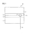
- Figure 1 illustrates a process for producing an AlGaInP Thin-film light-emitting diode 10.
- solder layers 13, 14 may be the surfaces completely cover the respective wafer 11, 12 or applied only to certain areas of the wafer surfaces become. For the described method, it is natural irrelevant which of the soldering metals on which of the two Wafer is applied.
- the laser beam 16 for example a Nd: YAG laser, becomes then at a wavelength through the carrier wafer 11 irradiated, in which the carrier wafer 11 for the laser beam 16 is permeable.
- the laser beam 16 the contact area 15 is focused between the two wafers.
- the power of the laser is selected so that the two solder layers 13, 14 melt locally around the focus of the laser, so that the two solders connect with each other and after cooling and solidification of the locally heated portion 17, a local solder joint between the two wafers 11 and 12 exists.
- the laser can be operated both in continuous operation, as well as pulsed.
- the wavelength of the laser beam to adapt to the carrier wafer is at least partially transparent to the laser beam.
- the epitaxial disc can have a Laser diode layer or a detector layer included.
- the specified method for soldering temperature-sensitive components suitable because the heating not the entire wafer arrangement, but only one locally limited area 17.
- the wafer arrangement After joining the two wafers 11, 12, the wafer arrangement to individual components - for example, individual LED chips - to be isolated. This can be, for example done by sawing or breaking the arrangement.
- the finished one Component can be electrically from the side of the carrier wafer 11 ago be contacted.
- the solders 13, 14 are preferred then electrically conductive.
- Figure 2 shows a schematic plan view of the contact area 15 between two wafers.
- the two wafers are only on selected connection regions 21 of the contact region 15th soldered together.
- connection areas 21 find also connection-free areas 22 of the contact area 15, where no connection between the two wafers consists.
- soldering metals either only at the connection areas 21 on the wafer, or the Solders distributed over the entire contact area 15 to apply to the wafer surfaces.
- connection areas 21 and the connection-free areas 22 can thereby, depending on the requirements of the wafer arrangement adapted become.
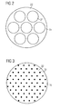
- FIG. 3 shows a plan view of the contact region 15 of FIG Wafer arrangement described here.
- the connection points 31 are at the Nodes of a regular network arranged.
- the connection-free Area 32 takes a much larger area of the contact area 15 as the total area of the connection points 31 is.
- soldering metals either only at the connection points 31 on the wafers, or the soldering metals over the entire contact area 15 on the wafer surfaces applied.
- connection points 31 are doing the requirements of the wafer arrangement and the requirements of adjusted the manufactured component. After separating The Waferanordung can in this embodiment components resulting from the side of the carrier wafer 11 Her only pointwise electrically contacted.
- the temperature load is particularly low, this wafer arrangement
- at least one of the wafers is a temperature-sensitive component includes. Because with pointwise connection of the two wafers finds only a few places in the wafer arrangement a lower Temperature entry into the wafer instead of and the total temperature entry is very low.
- connection point 31 or per connection area 21 exactly one component results. This means, It is possible that, for example, bodies where the wafer assembly is to be isolated (for example, predetermined breaking points or sawing channels), the wafers 11, 12 not with each other get connected. Only where components are created should then find a connection of the two wafers 11, 12th instead of.
Landscapes
- Engineering & Computer Science (AREA)
- Physics & Mathematics (AREA)
- Condensed Matter Physics & Semiconductors (AREA)
- General Physics & Mathematics (AREA)
- Manufacturing & Machinery (AREA)
- Computer Hardware Design (AREA)
- Microelectronics & Electronic Packaging (AREA)
- Power Engineering (AREA)
- Wire Bonding (AREA)
- Recrystallisation Techniques (AREA)
Abstract
Description
Diese Patentanmeldung beansprucht die Priorität der deutschen Patentanmeldungen 102004009625.2-11 und 102004012013.7-33, deren Offenbarungsgehalt hiermit durch Rückbezug aufgenommen wird.This patent application claims the priority of the German Patent Applications 102004009625.2-11 and 102004012013.7-33, the contents of which are hereby incorporated by reference becomes.
Die Erfindung betrifft ein Verfahren zum Verbinden zweier Wafer. Darüber hinaus betrifft die Erfindung eine Waferanordnung.The invention relates to a method for connecting two wafers. Moreover, the invention relates to a wafer arrangement.
Aus der Druckschrift US 6 284 998 B1 ist ein Verfahren zum
Auflöten eines elektronischen Bauelements auf ein dielektrisches
Substrat bekannt. Auf einer Oberfläche des Substrats
sind dazu mindestens zwei Anschlussstellen aus Metall vorgegeben,
die jeweils mit Lötpaste bedeckt werden. Im Folgenden
werden die Anschlüsse des elektronischen Bauelements mit den
Anschlussstellen auf dem Substrat in Kontakt gebracht. Der
Strahl eines Diodenlasers wird dann so lange durch die, den
Anschlussstellen gegenüberliegende Seite des Substrats auf
jeweils eine der metallischen Anschlussstellen gerichtet, bis
die Lötpaste auf der Anschlussstelle schmilzt. Die Wellenlänge
des Laserstrahls wird dabei so gewählt, dass die Laserenergie
hauptsächlich von der Anschlussstelle und nicht vom
dielektrischen Substrat absorbiert wird.
Nach Abkühlen der Anschlussstelle besteht eine Lötverbindung
zwischen der Anschlussstelle und dem Anschluss des elektronischen
Bauelements.US Pat. No. 6,284,998 B1 discloses a method for soldering an electronic component onto a dielectric substrate. For this purpose, at least two connection points made of metal, which are each covered with soldering paste, are provided on a surface of the substrate. In the following, the connections of the electronic component are brought into contact with the connection locations on the substrate. The beam of a diode laser is then directed so long through the, the connection points opposite side of the substrate on each one of the metallic connection points until the solder paste melts on the connection point. The wavelength of the laser beam is chosen so that the laser energy is absorbed mainly by the junction and not by the dielectric substrate.
After cooling the connection point there is a solder connection between the connection point and the connection of the electronic component.
Die Druckschrift DE 103 03 978 A1 beschreibt ein Verfahren zur Herstellung eines Halbleiterbauelements, bei dem ein werden jeweils auf Dünnfilmhalbleiterkörper und Träger Lötmetalle aufgebracht. Dünnfilmhalbleiterkörper und Träger werden dann unter erhöhtem Druck, bei einer Temperatur, die über dem Schmelzpunkt der beteiligten Lötmetalle liegt, zusammengefügt.The document DE 103 03 978 A1 describes a method for producing a semiconductor device, wherein a are each on thin-film semiconductor body and carrier solders applied. Thin-film semiconductor body and carrier become then under increased pressure, at a temperature above that Melting point of the solders involved, joined together.
Aufgabe der vorliegenden Erfindung ist es, ein Verfahren zum
möglichst einfachen Verbinden zweier Wafer anzugeben.
Ferner ist es Aufgabe der Erfindung, eine Waferanordnung anzugeben.The object of the present invention is to provide a method for connecting two wafers as simply as possible.
It is another object of the invention to provide a wafer arrangement.
Diese Aufgaben werden gelöst durch ein Verfahren zum Verbinden zweier Wafer nach Patentanspruch 1 und ferner durch die Waferanordnung nach Patentanspruch 30. Vorteilhafte Ausgestaltungen der Erfindung sind Gegenstand von Unteransprüchen.These objects are achieved by a method of joining two wafers according to claim 1 and further by the Wafer arrangement according to claim 30. Advantageous embodiments The invention are the subject of subclaims.
Es wird ein Verfahren für das Verbinden zweier Wafer angegeben. Dazu wird zwischen den beiden Wafern ein Kontaktbereich gebildet, indem die beiden Wafer übereinander gelegt werden. Die Verbindung zwischen den Wafern findet durch ein örtlich und zeitlich begrenztes Erhitzen des Kontaktbereichs der beiden Wafer statt.A method for connecting two wafers is given. For this purpose, a contact area between the two wafers formed by the two wafers are superimposed. The connection between the wafers takes place through a local and heating the contact area of the two for a limited time Wafers take place.
Örtlich begrenztes Erhitzen bedeutet in diesem Zusammenhang, dass eine nennenswerte Erwärmung der Wafer in einer Richtung parallel oder senkrecht zum Kontaktbereich, vorzugsweise in beide Richtungen, begrenzt bleibt. Nach Abkühlung sind beide Wafer dann an ihrem Kontaktbereich, am Ort der lokalen Erhitzung, mechanisch miteinander verbunden.Local heating in this context means that is a significant warming of the wafer in one direction parallel or perpendicular to the contact area, preferably in both directions, remains limited. After cooling, both are Wafers then at their contact area, at the place of local heating, mechanically interconnected.
In einer Ausführungsform des Verfahrens werden zwei Wafer bereitgestellt. Auf wenigstens eine der Waferoberflächen wird ein Material aufgebracht. Dabei kann das Material über die gesamte Waferoberfläche verteilt aufgebracht werden, oder das Material wird stellenweise auf ausgewählte Bereiche der Waferoberfläche aufgebracht, oder das Material wird über die gesamte Waferoberfläche verteilt aufgebracht und anschließend von ausgewählten Bereichen entfernt, beispielsweise weggeätzt. Anschließend wird ein Kontaktbereich zwischen den Wafern'hergestellt, indem die Wafer so übereinandergelegt werden, dass sich das aufgebrachte Material zwischen den Wafern befindet. Durch eine lokale und zeitlich begrenzte Erhitzung des Materials im Kontaktbereich entsteht dann eine mechanische Verbindung zwischen den Wafern, vermittelt durch das Material zwischen den Wafern.In one embodiment of the method, two wafers are provided. On at least one of the wafer surfaces is applied a material. Here, the material on the Whole wafer surface can be applied distributed, or the Material is applied in places to selected areas of the wafer surface Applied, or the material will over the entire Wafer surface spread applied and then removed from selected areas, for example etched away. Subsequently, a contact area is established between the wafers, by overlaying the wafers that the applied material is between the wafers located. Through a local and temporary heating of the material in the contact area then creates a mechanical Connection between the wafers, mediated by the material between the wafers.
Dabei kann das Material beispielsweise geeignet so gewählt werden, dass das Material durch das lokale Erhitzen zunächst aufschmilzt und beim Abkühlen unter Ausbildung eines Eutektikums mit dem Wafer-Material erstarrt.The material may, for example, suitably chosen so be that material by local heating first melts and on cooling to form a eutectic solidified with the wafer material.
In einer weiteren Ausführungsform des Verfahrens werden auf die Oberflächen beider Wafer Materialien aufgebracht. Dabei unterscheidet sich das Material, das auf den ersten Wafer aufgebracht wird, vom Material, das auf den zweiten Wafer aufgebracht wird.In a further embodiment of the method are on the surfaces of both wafer materials applied. there the material that differs on the first wafer differs is applied from the material on the second wafer is applied.
Die Materialien müssen dabei nicht unbedingt auf die gesamte Waferoberfläche aufgebracht werden, sondern können auch stellenweise, auf ausgewählte Bereiche der Waferoberfläche, aufgebracht werden.The materials do not necessarily have to be on the whole Wafer surface can be applied, but also in places, on selected areas of the wafer surface, applied become.
Die beiden Wafer werden nachfolgend in solcher Weise übereinandergelegt, dass sich die Materialien zwischen den Wafern befinden. Die Materialien werden dann im so hergestellten Kontaktbereich zwischen den Wafern örtlich und zeitlich begrenzt erhitzt, so dass sich die beiden verschiedenen Materialen im Bereich der Erwärmung verbinden. Dies kann beispielsweise dadurch geschehen, dass die beiden Materialen aufschmelzen und sich die Materialen in der Schmelze durchmischen. Auch eine erhöhte Mobilität der Teilchen aufgrund der Erwärmung ist denkbar, so dass durch Teilchendiffusion eine Durchmischung der Materialen stattfindet.The two wafers are subsequently superimposed in such a way that the materials are between the wafers are located. The materials are then produced in this way Contact area between the wafers limited in time and place heated so that the two different materials connect in the area of heating. This can be, for example This is done by melting the two materials and mix the materials in the melt. Also an increased mobility of the particles due to the Heating is conceivable, so that by particle diffusion Mixing of the materials takes place.
In jedem Fall entsteht nach dem örtlich und zeitlich begrenzten Erhitzen des Kontaktbereichs eine mechanische Verbindung zwischen den Wafern, vermittelt durch die Materialien zwischen den Wafern.In any case arises after the locally and temporally limited Heating the contact area a mechanical connection between the wafers, mediated by the materials between the wafers.
In einer bevorzugten Ausführungsform der Erfindung handelt es sich bei den Materialien, die auf die Waferoberflächen am Kontaktbereich aufgebracht werden, um Lote.In a preferred embodiment of the invention is with the materials that are on the wafer surfaces at Contact area can be applied to solders.
In einer besonders bevorzugten Ausführungsform handelt es sich bei den Loten um Lötmetalle. Bevorzugt finden dabei die folgenden Lötmetalle im Verfahren Anwendung: Au, AuSn, Pd, In, Pt.In a particularly preferred embodiment it is the solders are soldered. Preferably find the following solders in the process Application: Au, AuSn, Pd, In, Pt.
Beim lokalen Erhitzen des Kontaktbereichs schmelzen diese Lötmetalle auf und vermischen sich. Nach Abkühlen und Erstarren der Lotschicht besteht dann eine mechanische Verbindung zwischen den Wafern.Upon local heating of the contact area, they melt Solders on and mix. After cooling and solidification The solder layer is then a mechanical connection between the wafers.
In einer bevorzugten Ausführungsform des Verfahrens zum Verbinden
zweier Wafer wird der Kontaktbereich zwischen den Wafern
mittels wenigstens eines Laserstrahls lokal erhitzt.
Für das Prinzip des Verfahrens ist es dabei unerheblich, ob
ein einzelner Laserstrahl in zeitlicher Abfolge, Stelle für
Stelle, oder etwa eine Vielzahl von Laserstrahlen gleichzeitig
an unterschiedlichen Stellen des Kontaktbereichs zum Einsatz
kommen.In a preferred embodiment of the method for connecting two wafers, the contact area between the wafers is locally heated by means of at least one laser beam.
For the principle of the method, it is irrelevant whether a single laser beam in time sequence, position by point, or about a plurality of laser beams are used simultaneously at different locations of the contact area.
Die Wellenlänge des Lasers und mindestens einer der Wafer sind dabei so aneinander angepasst, dass wenigstens einer der Wafer für den Laserstrahl zumindest teilweise durchlässig ist. Das heißt, dass allenfalls eine geringfügige Absorption der Energie des Laserstrahls im Wafer stattfindet.The wavelength of the laser and at least one of the wafers are adapted to each other so that at least one of Wafer for the laser beam at least partially transparent is. That means that at most a slight absorption the energy of the laser beam in the wafer takes place.
Der Laserstrahl wird dann durch wenigstens einen den Wafer hindurch auf den Kontaktbereich zwischen den Wafern fokussiert.The laser beam is then passed through at least one wafer focused on the contact area between the wafers.
Der Laserstrahl wird, in einer besonders bevorzugten Ausführungsform, im überwiegenden Maße von dem Material oder den Materialien am Kontaktbereich zwischen den Wafern absorbiert. Dies kann zum Beispiel dadurch geschehen, dass die Materialien am Kontaktbereich für den Laserstrahl überwiegend nicht transparent sind und die Energie des Laserstrahls absorbieren. Dadurch ist gewährleistet, dass der Kontaktbereich erhitzt wird und zwar lokal begrenzt um den Bereich herum, auf den der Fokus des Laserstrahls gerichtet ist. Die Leistung des Lasers ist dabei vorzugsweise ausreichend hoch zu wählen, so dass nach Abkühlung eine mechanische Verbindung der beiden Wafer am Kontaktbereich erfolgt ist.The laser beam is, in a particularly preferred embodiment, in the vast majority of the material or the Materials absorbed at the contact area between the wafers. This can be done, for example, by the materials At the contact area for the laser beam mostly not transparent and absorb the energy of the laser beam. This ensures that the contact area is heated is locally limited around the area, on the focus of the laser beam is directed. The performance the laser is preferably sufficiently high to choose so that after cooling a mechanical connection of the two Wafer at the contact area is done.
In einer Ausführungsform des Verfahrens kann der Laser dabei im Dauerbetrieb betrieben werden.In one embodiment of the method, the laser can thereby be operated in continuous operation.
Für eine bevorzugte Ausführungsform des Verfahrens ist ein Laser im gepulsten Betrieb zweckmäßig. Durch eine entsprechende Wahl von Impulsdauer und Impulsabstand kann dabei der Abtransport der an der Kontaktfläche entstehenden Wärme optimal eingestellt werden. Es kann also mit einem Laser im Pulsbetrieb die örtliche Begrenzung der Erhitzung besonders leicht erreicht werden. Auch die gewünschte zeitliche Begrenzung der Erhitzung ist bei einem pulsbetriebenen Laser durch die begrenzte Impulsdauer gegeben. Zum Erzeugen der Laserstrahlen kommt dabei in einer möglichen Ausführungsform des Verfahrens ein Nd:YAG Laser zum Einsatz.For a preferred embodiment of the method is a Laser in pulsed operation appropriate. By an appropriate Choice of pulse duration and pulse spacing can be the Removal of heat generated at the contact surface optimally be set. So it can be done with a laser Pulse operation the local limit of heating especially be easily reached. Also the desired time limit Heating is on a pulse-powered laser given the limited pulse duration. For generating the laser beams comes in a possible embodiment of the Procedure a Nd: YAG laser used.
In einer weitern Ausführungsform des beschriebenen Verfahrens
wird der Laserstrahl kontinuierlich über den gesamten Kontaktbereich
zwischen den wafern geführt.
Auf diese Weise werden alle Bereiche des Kontaktbereichs örtlich
begrenzt erhitzt und es entsteht über den gesamten Kontaktbereich
beider Wafer eine flächige, mechanische Verbindung
zwischen den beiden Wafern. Die lokalen Erhitzungen des
Kontaktbereichs, können dabei in zeitlicher Abfolge durch einen
einzelnen Laserstrahl erfolgen oder, bei Verwendung einer
Vielzahl von Laserstrahlen, an mehreren lokalen Bereichen des
Kontaktbereichs gleichzeitig.In another embodiment of the described method, the laser beam is continuously guided over the entire contact area between the wafers.
In this way, all areas of the contact area are heated locally and over the entire contact area of both wafers a flat, mechanical connection between the two wafers is produced. The local heating of the contact region can be effected in chronological order by a single laser beam or, if a plurality of laser beams are used, at several local regions of the contact region simultaneously.
In einer anderen Ausführungsform des Verfahrens wird der Laser
über ausgewählte Bereiche des Kontaktbereichs geführt, so
dass nur in diesen ausgewählten Bereichen eine Verbindung
zwischen den beiden Wafern hergestellt wird. Es wird dabei
also eine Verbindung zwischen beiden Wafern in ausgewählten
Stellen des Kontaktbereichs erreicht, während andere Bereiche
des Kontaktbereichs zwischen den Wafern ohne durch direkte
Erwärmung hergestellte Verbindung bleiben. Dabei können Form,
Anordnung, Anzahl und Größe der Verbindungsbereiche und der
verbindungsfreien Bereiche je nach den Erfordernissen des
Produkts ausgebildet sein.
Das heißt, Form, Anordnung, Anzahl und Größe von Verbindungsbereichen
und verbindungsfreien Bereichen können beispielsweise
der erforderlichen Temperaturbeständigkeit, der bevorzugten
mechanischen Stabilität, der Funktionsweise des Bauelements,
oder auch den gewünschten Kosten des Produkts angepasst
werden.In another embodiment of the method, the laser is guided over selected regions of the contact region, so that a connection between the two wafers is produced only in these selected regions. Thus, a connection between both wafers is achieved in selected locations of the contact area, while other areas of the contact area between the wafers remain without a connection made by direct heating. In this case, the shape, arrangement, number and size of the connection areas and the connection-free areas can be formed depending on the requirements of the product.
That is, the shape, arrangement, number and size of connection areas and connection-free areas can be adapted for example to the required temperature resistance, the preferred mechanical stability, the operation of the device, or even the desired cost of the product.
Auch in dieser Ausführungsform des Verfahrens ist es natürlich möglich, einen einzelnen Laserstrahl oder eine Vielzahl von Laserstrahlen einzusetzen.Also in this embodiment of the method it is natural possible, a single laser beam or a variety of laser beams.
In einer weitern Ausführungsform des Verfahrens erfolgt die Verbindung beider Wafer am Kontaktbereich punktweise. Dazu wird der Laserstrahl nur auf einzelne, vorgegebene Stellen des Kontaktbereichs fokussiert. An diesen Stellen kommt es dabei zu einer Verbindung zwischen den beiden Wafern. Dabei können die einzelnen Verbindungspunkte vorteilhaft an den Knotenpunkten eines regelmäßigen Netzwerks angeordnet werden. Anzahl der Verbindungspunkte und Ausgestaltung des Netzwerks können dabei an die Erfordernisse des Produkts angepasst werden.In a further embodiment of the method, the Connection of both wafers at the contact area pointwise. To The laser beam is only on individual, predetermined locations focused on the contact area. In these places it comes thereby to a connection between the two wafers. there the individual connection points can be advantageous to the Nodes of a regular network can be arranged. Number of connection points and configuration of the network can be adapted to the requirements of the product.
Auch in dieser Ausführungsform ist es möglich einen Laserstrahl in zeitlicher Abfolge oder eine Vielzahl von Lasern gleichzeitig einzusetzen. Insbesondere ist es hier möglich, dass die Zahl der Laserstrahlen der Zahl der gewünschten Verbindungspunkte entspricht.Also in this embodiment, it is possible a laser beam in chronological order or a variety of lasers use at the same time. In particular, it is possible here that the number of laser beams is the number of desired connection points equivalent.
In einer besonders bevorzugten Ausführungsform des Verfahrens wird nur auf solche Bereiche des Kontaktbereichs Material aufgebracht, die danach vom Laserstrahl bestrahlt werden. Beispielsweise wird für den Fall einer punktweisen Verbindung beider Wafer nur an diesen Punkten vorher Material aufgebracht. In a particularly preferred embodiment of the method only applies to such areas of the contact area material applied, which are then irradiated by the laser beam. For example, in the case of a point-to-point connection both wafers applied material only at these points before.
Bei einer Ausführungsform des beschriebenen Verfahrens enthält wenigstens einer der Wafer ein Halbleitermaterial.In one embodiment of the method described at least one of the wafers is a semiconductor material.
In einer weitern Ausführungsform des Verfahrens zum Verbinden zweier Wafer, enthält wenigstens einer der Wafer eines der folgenden Halbleitermaterialien: Silizium, Germanium, Galliumarsenid, InP, GaP.In a further embodiment of the method for joining of two wafers, at least one of the wafers contains one of the wafers following semiconductor materials: silicon, germanium, gallium arsenide, InP, GaP.
In einer Ausführungsform des Verfahrens enthält wenigstens einer der Wafer wenigstens eines der folgenden Metalle: Mo, Cu, CuW. Auch kann wenigstens einer der Wafer in einer weiteren Ausführungsform des Verfahrens keramische Materialen enthalten.In one embodiment of the method contains at least one of the wafers of at least one of the following metals: Mo, Cu, CuW. Also, at least one of the wafers in another Embodiment of the method contain ceramic materials.
In einer Ausführungsform des Verfahrens umfasst wenigstens einer der Wafer eine Mehrzahl von Einzelschichten, wobei wenigstens eine der Einzelschichten eine epitaktisch aufgebrachte Schicht ist.In one embodiment of the method, at least one of the wafers has a plurality of individual layers, wherein at least one of the individual layers is epitaxially applied Layer is.
In einer weiteren Ausführungsform des Verfahrens enthält die epitaktisch aufgebrachte Schicht vorzugsweise eines der folgenden Halbleitermaterialen: GaInN, AlGaAs, AlGaInP, GaP, InP, InGaAs, InGaAsP, GaN, AlGaInN.In a further embodiment of the method, the epitaxially deposited layer preferably one of the following Semiconductor materials: GaInN, AlGaAs, AlGaInP, GaP, InP, InGaAs, InGaAsP, GaN, AlGaInN.
Dabei bildet in einer bevorzugten Ausführungsform des Verfahrens wenigstens eine Einzelschicht des Wafers ein elektronisches oder mikroelektronisches Bauelement.It forms in a preferred embodiment of the method at least a single layer of the wafer is an electronic one or microelectronic device.
Hierbei sind Ausführungsformen besonders bevorzugt, bei denen das elektronische Bauelement ein optoelektronisches Bauelement bildet, beispielsweise eine Leuchtdiode, einen Halbleiterlaser oder einen Detektor (z.B. Photodiode). In this case, embodiments are particularly preferred in which the electronic component is an optoelectronic component forms, for example, a light emitting diode, a semiconductor laser or a detector (e.g., photodiode).
Weiter betrifft die Erfindung eine Waferanordnung, bei der zwei übereinanderliegende Wafer an ausgewählten Bereichen ihres Kontaktbereichs miteinander verbunden sind.Furthermore, the invention relates to a wafer arrangement in which two superimposed wafers on selected areas of their Contact area are interconnected.
Diese Verbindung kann beispielsweise durch ein Material, oder zwei verschiedene Materialen zwischen den Wafer vermittelt werden.This compound may be, for example, a material, or mediates two different materials between the wafers become.
Der Waferanordnung liegt dabei die Idee zugrunde, dass sich die Verbindung beider Wafer nicht über den gesamten Kontaktbereich beider Wafer flächig erstreckt, sondern die beiden Wafer nur an ausgewählten Stellen ihres Kontaktbereichs miteinander verbunden sind. Dabei können die Materialen, die die Verbindung zwischen den Wafern vermitteln, entweder im gesamten Kontaktbereich aufgebracht sein, oder nur an jenen Stellen des Kontaktbereichs, an denen sich eine Verbindung zwischen den Wafern befindet.The wafer arrangement is based on the idea that the connection of both wafers not over the entire contact area both wafers flat, but the two Wafers only at selected points of their contact area with each other are connected. Thereby, the materials that the Communicate between the wafers, either throughout Be applied contact area, or only in those places of the contact area, which is a connection between located on the wafers.
Bei einer Ausführungsform der Waferanordnung sind die beiden Wafer an ihrem Kontaktbereich punktweise, an Verbindungspunkten, miteinander verbunden. Hierbei ist die Summe der Flächen des Kontaktbereichs, an denen die beiden Wafer miteinander verbunden sind, klein gegenüber der Summe der Flächen des Kontaktbereichs, in denen keine Verbindung zwischen den beiden Wafern besteht.In one embodiment of the wafer arrangement, the two are Wafer at its contact point pointwise, at connection points, connected with each other. Here is the sum of the areas the contact area at which the two wafers together are small compared to the sum of the areas of the Contact area where no connection between the two Wafern exists.
In einer bevorzugten Ausführungsform der Waferanordnung sind die Verbindungspunkte dabei an den Knoten eines regelmäßigen Netzwerks angeordnet.In a preferred embodiment of the wafer arrangement the connection points thereby to the nodes of a regular Network arranged.
In einer besonders bevorzugten Ausführungsform der beschriebenen Waferanordnung beinhaltet zumindest einer der Wafer eine besonders temperaturempfindliche Schicht. Das heißt, dass die maximale Temperatur, auf welche diese Schicht ohne Beschädigung erwärmt werden kann, kleiner ist als beispielsweise die Temperatur, bei der sich die Materialien am Kontaktbereich miteinander verbinden. In diesem Fall würde ein Erwärmen der gesamten Waferanordnung auf die Temperatur, bei der sich die Materialien verbinden, die temperaturempfindliche Schicht beschädigen.In a particularly preferred embodiment of the described Wafer assembly includes at least one of the wafers especially temperature-sensitive layer. It means that the maximum temperature to which this layer without damage can be heated is smaller than, for example the temperature at which the materials are at the contact area connect with each other. In this case, a warming would the entire wafer assembly to the temperature at which the materials combine, the temperature sensitive Damage layer.
Im folgenden werden das hier beschriebene Verfahren zum Verbinden
zweier Wafer und die beschriebene Waferanordnung anhand
von Ausführungsbeispielen und den dazugehörigen Figuren
näher erläutert:
Figur 1 erläutert ein Verfahren zur Herstellung einer AlGaInP
Dünnfilmleuchtdiode 10. Dazu werden beispielsweise ein GaAs
Träger-Wafer 11 und eine Epitaxiescheibe 12 mit einer AlGaInP
Leuchtdiodenschicht, die auf ein GaAs-Substrat epitaktisch
aufgebracht ist, bereitgestellt. Figure 1 illustrates a process for producing an AlGaInP
Thin-film light-emitting
Auf den Träger-Wafer 11 wird auf der Oberseite beispielsweise
eine AuSn-Lotschicht 13 aufgebracht. Auf die Epitaxiescheibe
12 wird auf die Unterseite beispielsweise eine Au-Lotschicht
14 aufgebracht. Die Lotschichten 13, 14 können die Oberflächen
der jeweiligen Wafer 11, 12 dabei komplett bedecken oder
nur auf bestimmte Bereiche der Wafer-Oberflächen aufgebracht
werden. Für das beschriebene Verfahren ist es dabei natürlich
unerheblich, welches der Lötmetalle auf welchen der beiden
Wafer aufgebracht wird.On the
Dann wird durch das Übereinanderlegen der beiden Wafer ein
Kontaktbereich 15 erzeugt, so dass sich die Lötmetallschichten
13, 14 zwischen den beiden Wafern 11, 12 befinden und
einander berühren.Then, by superposing the two
Der Laserstrahl 16, beispielsweise eines Nd:YAG Lasers, wird
daraufhin bei einer Wellenlänge durch den Träger-Wafer 11
eingestrahlt, bei welcher der Träger-Wafer 11 für den Laserstrahl
16 durchlässig ist. Dabei wird der Laserstrahl 16 auf
den Kontaktbereich 15 zwischen den beiden Wafern fokussiert.
Es ist darüber hinaus aber auch möglich, dass der Laserstrahl
16 durch die Epitaxiescheibe 12 hindurch auf die Kontaktschicht
15 fokussiert wird.The
Die Leistung des Lasers ist dafür so gewählt, dass die beiden
Lotschichten 13, 14 lokal um den Fokus des Lasers herum aufschmelzen,
so dass sich die beiden Lote miteinander verbinden
und nach Abkühlung und Erstarrung des lokal erhitzen Bereichs
17 eine lokale Lötverbindung zwischen den beiden Wafern 11
und 12 besteht.
Der Laser kann dabei sowohl im Dauerbetrieb, als auch gepulst
betrieben werden. The power of the laser is selected so that the two
The laser can be operated both in continuous operation, as well as pulsed.
Wird der Laserstrahl dabei kontinuierlich über den gesamten
Kontaktbereich 15 geführt, so entsteht eine flächige Lötverbindung
zwischen den beiden Wafern 11, 12.If the laser beam is continuously over the
Es versteht sich, dass neben dem genannten GaAs Wafer auch noch andere Träger-Wafer in Betracht kommen. Möglich ist beispielsweise auch die Verwendung von Wafern, die Germanium oder Silizium beinhalten. Gegebenenfalls ist dann die Wellenlänge des Laserstrahls so anzupassen, dass der Träger-Wafer für den Laserstrahl zumindest teilweise transparent ist.It is understood that in addition to the aforementioned GaAs wafer also still other carrier wafers come into consideration. Possible, for example also the use of wafers, the germanium or Include silicon. Optionally, then the wavelength of the laser beam to adapt to the carrier wafer is at least partially transparent to the laser beam.
Auch bei der Wahl der Epitaxiescheibe gibt es zahlreiche Möglichkeiten.
So kann die Epitaxiescheibe beispielsweise eine
Laserdiodenschicht oder eine Detektorschicht enthalten. Insbesondere
ist das angegebene Verfahren für das Verlöten von
temperaturempfindlichen Bauelementen geeignet, da die Erwärmung
nicht die gesamte Waferanordnung, sondern nur einen örtlich
begrenzten Bereich 17 betrifft.Also in the choice of epitaxial disc there are numerous possibilities.
For example, the epitaxial disc can have a
Laser diode layer or a detector layer included. Especially
is the specified method for soldering
temperature-sensitive components suitable because the heating
not the entire wafer arrangement, but only one locally
limited
Auch ist das beschriebene Verfahren hinsichtlich der Wahl der Lötmetalle nicht eingeschränkt. Da im beschriebenen Verfahren die Wärmebelastung lokal auf den Kontaktbereich zwischen den Wafern beschränkt ist, sind insbesondere Kombinationen von Lötmetallen denkbar, die sich erst bei viel höheren Temperaturen als die angegebnen Au und AuSn Lote verbinden.Also, the method described in terms of the choice of Solders not restricted. As described in the procedure the heat load locally on the contact area between the Wafern is limited, in particular combinations of Solders are conceivable, which are only at much higher temperatures as the specified Au and AuSn join Lote.
Nach dem Verbinden der beiden Wafer 11, 12 kann die Waferanordnung
zu einzelnen Bauelementen - beispielsweise einzelnen
Leuchtdiodenchips - vereinzelt werden. Dies kann zum Beispiel
mittels Sägen oder Brechen der Anordnung erfolgen. Das fertige
Bauelement kann von der Seite des Träger-Wafers 11 her elektrisch
kontaktiert werden. Bevorzugt sind die Lote 13, 14
dann elektrisch leitend. After joining the two
Figur 2 zeigt eine schematische Draufsicht auf den Kontaktbereich
15 zwischen zwei Wafern. Die beiden Wafer sind nur an
ausgewählten Verbindungsbereichen 21 des Kontaktbereichs 15
miteinander verlötet. Neben den Verbindungsbereichen 21 finden
sich auch verbindungsfreie Bereiche 22 des Kontaktbereichs
15, an denen keine Verbindung zwischen den beiden Wafern
besteht.Figure 2 shows a schematic plan view of the
Dabei ist es möglich, die Lötmetalle entweder nur an den Verbindungsbereichen
21 auf die Wafer aufzubringen, oder die
Lötmetalle über den gesamten Kontaktbereich 15 verteilt auf
den Waferoberflächen aufzubringen.It is possible, the soldering metals either only at the
Form, Größe, Anzahl und Anordnung der ausgewählten Verbindungsbereiche
21 und der verbindungsfreien Bereiche 22 können
dabei, je nach den Erfordernissen der Waferanordnung, angepasst
werden.Shape, size, number and arrangement of the selected
Figur 3 zeigt eine Draufsicht auf den Kontaktbereich 15 der
hier beschriebenen Waferanordnung. Dabei sind die beiden Wafer
an Verbindungspunkten 31 des Kontaktbereichs 15 miteinander
verbunden. Die Verbindungspunkte 31 sind dabei an den
Knoten eines regelmäßigen Netzwerks angeordnet. Der verbindungsfreie
Bereich 32 nimmt dabei eine weitaus größere Fläche
des Kontaktbereichs 15 ein, als die Gesamtfläche der Verbindungspunkte
31 beträgt.FIG. 3 shows a plan view of the
Dabei ist es möglich die Lötmetalle entweder nur an den Verbindungspunkten
31 auf die Wafer aufzubringen, oder die Lötmetalle
über den gesamten Kontaktbereich 15 auf den Waferoberflächen
aufzubringen. It is possible, the soldering metals either only at the connection points
31 on the wafers, or the soldering metals
over the
Anzahl und Anordnung der Verbindungspunkte 31 werden dabei an
die Erfordernisse der Waferanordnung und die Anforderungen an
das herzustellende Bauelement angepasst. Nach dem Vereinzeln
der Waferanordung können in diesem Ausführungsbeispiel Bauelemente
resultieren, die von der Seite des Träger-Wafers 11
her nur punktweise elektrisch kontaktiert sind.Number and arrangement of the connection points 31 are doing
the requirements of the wafer arrangement and the requirements of
adjusted the manufactured component. After separating
The Waferanordung can in this embodiment components
resulting from the side of the
Da bei einer punktweisen Verbindung beider Wafer, die Temperaturbelastung besonders gering ist, ist diese Waferanordnung beispielsweise dann besonders geeignet, wenn zumindest einer der Wafer ein temperaturempfindliches Bauteil beinhaltet. Denn bei punktweisen Verbinden der beiden Wafer findet nur an wenigen Stellen der Waferanordnung ein geringer Temperatureintrag in die Wafer statt und der insgesamte Temperatureintrag ist dabei sehr gering.As with a pointwise connection of both wafers, the temperature load is particularly low, this wafer arrangement For example, then particularly suitable if at least one of the wafers is a temperature-sensitive component includes. Because with pointwise connection of the two wafers finds only a few places in the wafer arrangement a lower Temperature entry into the wafer instead of and the total temperature entry is very low.
Auch ist es in den beiden letztgenannten Ausführungsbeispielen
möglich, dass pro Verbindungspunkt 31 oder pro Verbindungsbereich
21 genau ein Bauelement resultiert. Das heißt,
es ist möglich, dass beispielsweise Stellen, an denen die Waferanordnung
vereinzelt werden soll (beispielsweise Sollbruchstellen
oder Sägekanäle), die Wafer 11, 12 nicht miteinander
verbunden werden. Nur dort, wo Bauelemente entstehen
sollen, findet dann ein Verbinden der beiden Wafer 11, 12
statt.It is also in the two last-mentioned embodiments
possible that per
Die Erfindung ist nicht durch die Beschreibung anhand der Ausführungsbeispiele beschränkt. Vielmehr umfasst die Erfindung jedes neue Merkmal sowie jede Kombination von Merkmalen, was insbesondere jede Kombination von Merkmalen in den Patentansprüchen beinhaltet, auch wenn dieses Merkmal oder diese Kombination selbst nicht explizit in den Patentansprüchen oder Ausführungsbeispielen angegeben ist.The invention is not by the description based on the Embodiments limited. Rather, the invention includes every new feature and every combination of features, which in particular any combination of features in the claims includes, even if this feature or this Combination itself not explicitly in the claims or embodiments is given.
Claims (34)
bei dem durch Übereinanderlegen der beiden Wafer ein Kontaktbereich (15) zwischen den Wafern (11,12) gebildet wird und bei dem der Kontaktbereich (15) örtlich und zeitlich begrenzt erhitzt wird.Method for connecting two wafers (11, 12),
in which, by superimposing the two wafers, a contact region (15) is formed between the wafers (11, 12) and in which the contact region (15) is heated locally and for a limited time.
mit folgenden Schritten:
with the following steps:
bei dem das Material (13,14) so beschaffen ist, dass nach Erhitzen und Abkühlen des Materials (13,14) eine mechanische Verbindung zwischen den Wafern (11,12) hergestellt ist.Method according to claim 2,
in which the material (13, 14) is such that, after heating and cooling of the material (13, 14), a mechanical connection between the wafers (11, 12) is produced.
bei dem nach Erhitzen und Abkühlen des Materials (13,14) eine Legierung des Materials (13,14) mit wenigstens einem der Wafer (11,12) besteht:Method according to claim 2,
in which, after the material (13, 14) has been heated and cooled, an alloy of the material (13, 14) with at least one of the wafers (11, 12) is formed:
bei dem Materialien (13,14) auf beide Wafer (11,12) aufgebracht werden, wobei sich das Material (13), das auf den ersten Wafer aufgebracht wird, vom Material (14), das auf den zweiten Wafer aufgebracht wird, unterscheidet. Method according to one of claims 1 or 2,
in which materials (13, 14) are applied to both wafers (11, 12), wherein the material (13) applied to the first wafer differs from the material (14) applied to the second wafer ,
bei dem sich die unterschiedlichen Materialien (13,14) bei Erwärmung durchmischen und nach Abkühlung eine mechanische Verbindung zwischen den Wafern (11,12) herstellen.Method according to claim 5,
in which the different materials (13,14) mix when heated and produce a mechanical connection between the wafers (11,12) after cooling.
bei dem es sich bei den Materialien (13,14) um Lote handelt.Method according to one of claims 2 to 6,
in which the materials (13, 14) are solders.
bei dem die Lote aus den folgenden Materialien (13,14) ausgewählt werden: Au, AuSn, Pd, In, Pt.Method according to claim 7,
in which the solders are selected from the following materials (13, 14): Au, AuSn, Pd, In, Pt.
bei dem die lokale Erhitzung des Kontaktbereichs mittels wenigstens eines Laserstrahls (16) vorgenommen wird.Method according to one of claims 1 to 8,
in which the local heating of the contact region is carried out by means of at least one laser beam (16).
bei dem die Wellenlänge des Laserstrahls (16) und wenigstens einer der Wafer (11,12) so aneinander angepasst sind, dass der Wafer (11,12) für den Laser zumindest teilweise durchlässig ist.Method according to claim 9,
in which the wavelength of the laser beam (16) and at least one of the wafers (11, 12) are adapted to one another in such a way that the wafer (11, 12) for the laser is at least partially transmissive.
bei dem der Laserstrahl (16) durch wenigstens einen der Wafer (11,12) hindurch läuft und auf den Kontaktbereich (15) fokussiert wird.Method according to one of claims 9 or 10,
in which the laser beam (16) passes through at least one of the wafers (11, 12) and is focused onto the contact region (15).
bei dem die Leistung des Lasers so gewählt wird, dass am Kontaktbereich (15) eine mechanische Verbindung zwischen den beiden Wafern entsteht. Method according to one of claims 9 to 11,
in which the power of the laser is chosen such that a mechanical connection between the two wafers is created at the contact region (15).
bei dem der Laser im Dauerbetrieb betrieben wird.Method according to one of claims 9 to 12,
in which the laser is operated in continuous operation.
bei dem der Laser im Pulsbetrieb betrieben wird.Method according to one of claims 9 to 12,
in which the laser is operated in pulsed mode.
bei dem als Laser ein Nd:YAG Laser zum Einsatz kommt.Method according to one of claims 9 to 14,
using a laser as an Nd: YAG laser.
bei dem der Laserstrahl (16) kontinuierlich über den gesamten Kontaktbereich (15) geführt wird.Method according to one of claims 1 to 15,
in which the laser beam (16) is continuously guided over the entire contact area (15).
bei dem der Laserstrahl (16) über ausgewählte Bereiche des Kontaktbereichs (15) geführt wird.Method according to one of claims 1 to 15,
in which the laser beam (16) is guided over selected regions of the contact region (15).
bei dem der Laserstrahl (16) punktweise auf Bereiche des Kontaktbereichs (15) fokussiert wird, so dass Verbindungspunkte (31) zwischen den Wafern entstehen.Method according to claim 17,
in which the laser beam (16) is focused point by point on areas of the contact area (15), so that connecting points (31) are created between the wafers.
bei dem die Verbindungspunkte (31) an den Knoten eines regelmäßigen Netzwerks angeordnet werden.Method according to claim 18,
in which the connection points (31) are arranged at the nodes of a regular network.
bei dem die Zahl der Laserstrahlen (16) der Zahl der Verbindungspunkte (31) entspricht.Method according to one of claims 18 or 19,
in which the number of laser beams (16) corresponds to the number of connection points (31).
bei dem nur an den Bereichen des Kontaktbereichs (15) ein Material aufgebracht ist, die vom Laserstrahl (16) bestrahlt werden.Method according to one of claims 17 to 20,
in which only at the areas of the contact region (15) a material is applied, which are irradiated by the laser beam (16).
bei dem wenigstens einer der Wafer (11,12) wenigstens ein Halbleitermaterial enthält.Method according to one of claims 1 to 21,
in which at least one of the wafers (11, 12) contains at least one semiconductor material.
bei dem wenigstens einer der Wafer (11,12) mindestens eines der folgenden Halbleitermaterialien enthält: Silizium, Germanium, Galliumarsenid, InP, GaP.Method according to claim 22,
in which at least one of the wafers (11, 12) contains at least one of the following semiconductor materials: silicon, germanium, gallium arsenide, InP, GaP.
bei dem wenigstens einer der Wafer (11,12) eine Mehrzahl von Einzelschichten umfasst.Method according to one of claims 1 to 21,
wherein at least one of the wafers (11, 12) comprises a plurality of individual layers.
bei dem wenigstens eine der Einzelschichten eine epitaktisch aufgebrachte Schicht ist.Method according to claim 24,
in which at least one of the individual layers is an epitaxially applied layer.
bei dem die epitaktisch aufgebrachte Schicht wenigstens eines der folgenden Halbleitermaterialien enthält: GaInN, AlGaAs, AlGaInP, GaP, InP, InGaAs, InGaAsP, GaN, AlGaInN.Method according to claim 25,
in which the epitaxially deposited layer contains at least one of the following semiconductor materials: GaInN, AlGaAs, AlGaInP, GaP, InP, InGaAs, InGaAsP, GaN, AlGaInN.
bei dem wenigstens eine Einzelschicht des Wafers Teil eines optoelektronisches Bauelement ist.Method according to one of claims 23 to 26,
in which at least one single layer of the wafer is part of an optoelectronic component.
bei dem das optoelektronische Bauelement eine Leuchtdiode ist. Method according to claim 27,
in which the optoelectronic component is a light-emitting diode.
bei dem das optoelektronische Bauelement ein Halbleiterlaser ist.Method according to claim 27,
in which the optoelectronic component is a semiconductor laser.
bei dem das optoelektronische Bauelement ein Detektor ist.Method according to claim 27,
in which the optoelectronic component is a detector.
mit zwei übereinanderliegenden Wafern, zwischen denen sich ein Kontaktbereich (15) befindet, wobei die Wafer an ausgewählten Verbindungsbereichen (21) ihres Kontaktbereichs (15) miteinander verbunden sind.Wafer assembly,
with two superimposed wafers, between which a contact region (15) is located, wherein the wafers are connected to one another at selected connection regions (21) of their contact region (15).
bei der die beiden Wafer an ihrem Kontaktbereich (15) an Verbindungspunkten (31) miteinander verbunden sind.Wafer arrangement according to claim 31,
in which the two wafers are connected to one another at their contact region (15) at connection points (31).
bei der die Verbindungspunkte (31) an den Knoten eines regelmäßigen Netzwerks angeordnet sind.Wafer arrangement according to claim 32,
wherein the connection points (31) are arranged at the nodes of a regular network.
bei der mindestens einer der Wafer (11,12) wenigstens eine besonders temperaturempfindliche Schicht beinhaltet.Wafer arrangement according to one of claims 30 to 33,
in which at least one of the wafers (11, 12) contains at least one particularly temperature-sensitive layer.
Applications Claiming Priority (4)
| Application Number | Priority Date | Filing Date | Title |
|---|---|---|---|
| DE102004009625 | 2004-02-27 | ||
| DE102004009625 | 2004-02-27 | ||
| DE102004012013A DE102004012013B4 (en) | 2004-02-27 | 2004-03-11 | wafer assembly |
| DE102004012013 | 2004-03-11 |
Publications (3)
| Publication Number | Publication Date |
|---|---|
| EP1569263A2 true EP1569263A2 (en) | 2005-08-31 |
| EP1569263A3 EP1569263A3 (en) | 2009-05-06 |
| EP1569263B1 EP1569263B1 (en) | 2011-11-23 |
Family
ID=34751394
Family Applications (1)
| Application Number | Title | Priority Date | Filing Date |
|---|---|---|---|
| EP05002608A Expired - Fee Related EP1569263B1 (en) | 2004-02-27 | 2005-02-08 | Method for joining two wafers |
Country Status (3)
| Country | Link |
|---|---|
| US (2) | US7872210B2 (en) |
| EP (1) | EP1569263B1 (en) |
| JP (1) | JP2005244241A (en) |
Families Citing this family (2)
| Publication number | Priority date | Publication date | Assignee | Title |
|---|---|---|---|---|
| EP1569263B1 (en) * | 2004-02-27 | 2011-11-23 | OSRAM Opto Semiconductors GmbH | Method for joining two wafers |
| US10046408B2 (en) | 2015-05-28 | 2018-08-14 | Osram Opto Semiconductors Gmbh | Device comprising a connecting component and method for producing a connecting component |
Citations (16)
| Publication number | Priority date | Publication date | Assignee | Title |
|---|---|---|---|---|
| EP0232935A1 (en) * | 1986-01-30 | 1987-08-19 | Koninklijke Philips Electronics N.V. | Method of manufacturing a semiconductor device |
| GB2244374A (en) * | 1990-05-22 | 1991-11-27 | Stc Plc | Radiation beam bonding of semiconductor device contacts |
| EP0539741A1 (en) * | 1991-09-30 | 1993-05-05 | Canon Kabushiki Kaisha | Anodic bonding process with light irradiation |
| DE4219132A1 (en) * | 1992-06-11 | 1993-12-16 | Suess Kg Karl | Bonded silicon@ wafer-glass or silicon@-silicon@ joint prodn. - comprises using laser light radiation to initially fix materials at spot(s) and/or lines and conventional high temp. bonding for pressure and acceleration sensors or micro-system elements |
| US5460318A (en) * | 1994-06-01 | 1995-10-24 | Gte Laboratories Incorporated | Diebonding geometry for packaging optoelectronics |
| US5481082A (en) * | 1993-07-19 | 1996-01-02 | Mitsubishi Denki Kabushiki Kaisha | Apparatus and method for die bonding semiconductor element |
| US5500540A (en) * | 1994-04-15 | 1996-03-19 | Photonics Research Incorporated | Wafer scale optoelectronic package |
| EP0758145A2 (en) * | 1995-08-08 | 1997-02-12 | Taiyo Yuden Co., Ltd. | Method of manufacturing circuit module |
| DE19646476A1 (en) * | 1996-11-11 | 1998-05-14 | Fraunhofer Ges Forschung | Structure forming thermal connection for several components |
| US20010014514A1 (en) * | 1998-11-10 | 2001-08-16 | Joseph E Geusic | Low temperature silicon wafer bond process with bulk material bond strength |
| WO2002019439A1 (en) * | 2000-08-31 | 2002-03-07 | Osram Opto Semiconductors Gmbh | Method for producing a radiation-emitting semiconductor chip based on iii-v nitride semiconductor material, and a corresponding radiation-emitting semiconductor chip |
| US20020088979A1 (en) * | 1999-07-23 | 2002-07-11 | Hiroji Kawai | Semiconductor laminated substrate, semiconductor crystal substrate and semiconductor device and method of manufacturing the same |
| WO2003094224A1 (en) * | 2002-04-30 | 2003-11-13 | S.O.I.Tec Silicon On Insulator Technologies | Process for manufacturing substrates with detachment of a temporary support, and associated substrate |
| EP1369912A2 (en) * | 2002-06-03 | 2003-12-10 | Robert Bosch Gmbh | Method of mounting a Flip chip using a laser beam |
| US20040033638A1 (en) * | 2000-10-17 | 2004-02-19 | Stefan Bader | Method for fabricating a semiconductor component based on GaN |
| WO2004015756A1 (en) * | 2002-08-09 | 2004-02-19 | Sumitomo Electric Industries, Ltd. | Submount and semiconductor device |
Family Cites Families (49)
| Publication number | Priority date | Publication date | Assignee | Title |
|---|---|---|---|---|
| US3942244A (en) * | 1967-11-24 | 1976-03-09 | Semikron Gesellschaft Fur Gleichrichterbau Und Elektronik M.B.H. | Semiconductor element |
| US3939556A (en) * | 1971-11-04 | 1976-02-24 | Commissariat A L'energie Atomique | Liquid crystal cell |
| US3933556A (en) * | 1974-01-10 | 1976-01-20 | American Optical Corporation | Fiber optic image shape converter and method of making the same |
| US4772935A (en) * | 1984-12-19 | 1988-09-20 | Fairchild Semiconductor Corporation | Die bonding process |
| FR2576147B1 (en) * | 1985-01-17 | 1987-11-27 | Flicstein Jean | METHOD FOR DEPOSITING AND CRYSTALLIZING A THIN FILM OF ORGANIC MATERIAL USING AN ENERGY BEAM |
| US5037780A (en) * | 1989-02-02 | 1991-08-06 | Matsushita Electric Industrial Co., Ltd. | Method for attaching semiconductors to a transparent substrate using a light-curable resin |
| US6952301B2 (en) * | 1995-06-19 | 2005-10-04 | Reflectivity, Inc | Spatial light modulators with light blocking and absorbing areas |
| US6277696B1 (en) * | 1995-06-27 | 2001-08-21 | Hewlett-Packard Company | Surface emitting laser using two wafer bonded mirrors |
| JPH09193249A (en) * | 1995-08-15 | 1997-07-29 | Dainippon Ink & Chem Inc | Disk bonding method and apparatus |
| US5724376A (en) * | 1995-11-30 | 1998-03-03 | Hewlett-Packard Company | Transparent substrate vertical cavity surface emitting lasers fabricated by semiconductor wafer bonding |
| FR2748851B1 (en) * | 1996-05-15 | 1998-08-07 | Commissariat Energie Atomique | PROCESS FOR PRODUCING A THIN FILM OF SEMICONDUCTOR MATERIAL |
| DE19639438A1 (en) * | 1996-09-25 | 1998-04-02 | Siemens Ag | Semiconductor body with solder material layer |
| US6096155A (en) * | 1996-09-27 | 2000-08-01 | Digital Optics Corporation | Method of dicing wafer level integrated multiple optical elements |
| US6235141B1 (en) * | 1996-09-27 | 2001-05-22 | Digital Optics Corporation | Method of mass producing and packaging integrated optical subsystems |
| TW371364B (en) * | 1998-01-23 | 1999-10-01 | United Microelectronics Corp | Method for making buried diffusion junction |
| JP4085459B2 (en) * | 1998-03-02 | 2008-05-14 | セイコーエプソン株式会社 | Manufacturing method of three-dimensional device |
| JP4126749B2 (en) * | 1998-04-22 | 2008-07-30 | ソニー株式会社 | Manufacturing method of semiconductor device |
| JP2000003875A (en) * | 1998-06-12 | 2000-01-07 | Semiconductor Energy Lab Co Ltd | Semiconductor device and manufacture thereof |
| EP0964608A3 (en) | 1998-06-12 | 2001-09-05 | Ford Motor Company | Method for laser soldering |
| EP0981159A1 (en) | 1998-08-18 | 2000-02-23 | Siemens Building Technologies AG | Method for making microconnections, micrelectronic system, and infrared sensor manufactured using the method |
| US6214427B1 (en) * | 1998-08-28 | 2001-04-10 | General Electric Company | Method of making an electronic device having a single crystal substrate formed by solid state crystal conversion |
| US6328796B1 (en) * | 1999-02-01 | 2001-12-11 | The United States Of America As Represented By The Secretary Of The Navy | Single-crystal material on non-single-crystalline substrate |
| US6320206B1 (en) * | 1999-02-05 | 2001-11-20 | Lumileds Lighting, U.S., Llc | Light emitting devices having wafer bonded aluminum gallium indium nitride structures and mirror stacks |
| US6280523B1 (en) * | 1999-02-05 | 2001-08-28 | Lumileds Lighting, U.S., Llc | Thickness tailoring of wafer bonded AlxGayInzN structures by laser melting |
| US6406636B1 (en) * | 1999-06-02 | 2002-06-18 | Megasense, Inc. | Methods for wafer to wafer bonding using microstructures |
| US6576870B2 (en) * | 2000-11-13 | 2003-06-10 | Hannstar Display Corp. | Apparatus with double laser beams for cutting two bonded glass substrates and method thereof |
| US6594446B2 (en) * | 2000-12-04 | 2003-07-15 | Vortek Industries Ltd. | Heat-treating methods and systems |
| US6746889B1 (en) * | 2001-03-27 | 2004-06-08 | Emcore Corporation | Optoelectronic device with improved light extraction |
| JP2002359426A (en) * | 2001-06-01 | 2002-12-13 | Hitachi Ltd | Optical module and optical communication system |
| US6784462B2 (en) * | 2001-12-13 | 2004-08-31 | Rensselaer Polytechnic Institute | Light-emitting diode with planar omni-directional reflector |
| US6667225B2 (en) * | 2001-12-17 | 2003-12-23 | Intel Corporation | Wafer-bonding using solder and method of making the same |
| US6869820B2 (en) * | 2002-01-30 | 2005-03-22 | United Epitaxy Co., Ltd. | High efficiency light emitting diode and method of making the same |
| DE10303978A1 (en) | 2002-01-31 | 2003-11-27 | Osram Opto Semiconductors Gmbh | Semiconductor component used as a light emitting diode, especially an illuminating diode or laser diode, comprises a thin film semiconductor body arranged on a support containing germanium |
| US6762072B2 (en) * | 2002-03-06 | 2004-07-13 | Robert Bosch Gmbh | SI wafer-cap wafer bonding method using local laser energy, device produced by the method, and system used in the method |
| US6939778B2 (en) * | 2002-04-18 | 2005-09-06 | The Regents Of The University Of Michigan | Method of joining an insulator element to a substrate |
| US6767749B2 (en) * | 2002-04-22 | 2004-07-27 | The United States Of America As Represented By The Secretary Of The Navy | Method for making piezoelectric resonator and surface acoustic wave device using hydrogen implant layer splitting |
| AU2002307578A1 (en) * | 2002-04-30 | 2003-12-02 | Agency For Science Technology And Research | A method of wafer/substrate bonding |
| US20040016995A1 (en) * | 2002-07-25 | 2004-01-29 | Kuo Shun Meen | MEMS control chip integration |
| US6822326B2 (en) * | 2002-09-25 | 2004-11-23 | Ziptronix | Wafer bonding hermetic encapsulation |
| US6872983B2 (en) * | 2002-11-11 | 2005-03-29 | Finisar Corporation | High speed optical transceiver package using heterogeneous integration |
| JP4115859B2 (en) * | 2003-02-28 | 2008-07-09 | 株式会社日立製作所 | Anodic bonding method and electronic device |
| TWI222759B (en) * | 2003-07-03 | 2004-10-21 | Epitech Corp Ltd | Light emitting diode and method for manufacturing the same |
| US7186629B2 (en) * | 2003-11-19 | 2007-03-06 | Advanced Materials Sciences, Inc. | Protecting thin semiconductor wafers during back-grinding in high-volume production |
| TWI234211B (en) * | 2003-12-26 | 2005-06-11 | Advanced Semiconductor Eng | Method for forming an underfilling layer on a bumped wafer |
| US20060194690A1 (en) * | 2004-02-23 | 2006-08-31 | Hideyuki Osuzu | Alumina-based ceramic material and production method thereof |
| EP1569263B1 (en) * | 2004-02-27 | 2011-11-23 | OSRAM Opto Semiconductors GmbH | Method for joining two wafers |
| US7319048B2 (en) * | 2004-09-03 | 2008-01-15 | Intel Corporation | Electronic assemblies having a low processing temperature |
| US7244630B2 (en) * | 2005-04-05 | 2007-07-17 | Philips Lumileds Lighting Company, Llc | A1InGaP LED having reduced temperature dependence |
| DE102005048196B4 (en) * | 2005-07-29 | 2023-01-26 | OSRAM Opto Semiconductors Gesellschaft mit beschränkter Haftung | Radiation-emitting semiconductor chip |
-
2005
- 2005-02-08 EP EP05002608A patent/EP1569263B1/en not_active Expired - Fee Related
- 2005-02-25 JP JP2005051965A patent/JP2005244241A/en not_active Withdrawn
- 2005-02-28 US US11/068,291 patent/US7872210B2/en not_active Expired - Fee Related
-
2010
- 2010-12-13 US US12/966,555 patent/US8471385B2/en active Active
Patent Citations (16)
| Publication number | Priority date | Publication date | Assignee | Title |
|---|---|---|---|---|
| EP0232935A1 (en) * | 1986-01-30 | 1987-08-19 | Koninklijke Philips Electronics N.V. | Method of manufacturing a semiconductor device |
| GB2244374A (en) * | 1990-05-22 | 1991-11-27 | Stc Plc | Radiation beam bonding of semiconductor device contacts |
| EP0539741A1 (en) * | 1991-09-30 | 1993-05-05 | Canon Kabushiki Kaisha | Anodic bonding process with light irradiation |
| DE4219132A1 (en) * | 1992-06-11 | 1993-12-16 | Suess Kg Karl | Bonded silicon@ wafer-glass or silicon@-silicon@ joint prodn. - comprises using laser light radiation to initially fix materials at spot(s) and/or lines and conventional high temp. bonding for pressure and acceleration sensors or micro-system elements |
| US5481082A (en) * | 1993-07-19 | 1996-01-02 | Mitsubishi Denki Kabushiki Kaisha | Apparatus and method for die bonding semiconductor element |
| US5500540A (en) * | 1994-04-15 | 1996-03-19 | Photonics Research Incorporated | Wafer scale optoelectronic package |
| US5460318A (en) * | 1994-06-01 | 1995-10-24 | Gte Laboratories Incorporated | Diebonding geometry for packaging optoelectronics |
| EP0758145A2 (en) * | 1995-08-08 | 1997-02-12 | Taiyo Yuden Co., Ltd. | Method of manufacturing circuit module |
| DE19646476A1 (en) * | 1996-11-11 | 1998-05-14 | Fraunhofer Ges Forschung | Structure forming thermal connection for several components |
| US20010014514A1 (en) * | 1998-11-10 | 2001-08-16 | Joseph E Geusic | Low temperature silicon wafer bond process with bulk material bond strength |
| US20020088979A1 (en) * | 1999-07-23 | 2002-07-11 | Hiroji Kawai | Semiconductor laminated substrate, semiconductor crystal substrate and semiconductor device and method of manufacturing the same |
| WO2002019439A1 (en) * | 2000-08-31 | 2002-03-07 | Osram Opto Semiconductors Gmbh | Method for producing a radiation-emitting semiconductor chip based on iii-v nitride semiconductor material, and a corresponding radiation-emitting semiconductor chip |
| US20040033638A1 (en) * | 2000-10-17 | 2004-02-19 | Stefan Bader | Method for fabricating a semiconductor component based on GaN |
| WO2003094224A1 (en) * | 2002-04-30 | 2003-11-13 | S.O.I.Tec Silicon On Insulator Technologies | Process for manufacturing substrates with detachment of a temporary support, and associated substrate |
| EP1369912A2 (en) * | 2002-06-03 | 2003-12-10 | Robert Bosch Gmbh | Method of mounting a Flip chip using a laser beam |
| WO2004015756A1 (en) * | 2002-08-09 | 2004-02-19 | Sumitomo Electric Industries, Ltd. | Submount and semiconductor device |
Also Published As
| Publication number | Publication date |
|---|---|
| US20050211678A1 (en) | 2005-09-29 |
| US8471385B2 (en) | 2013-06-25 |
| US20110079911A1 (en) | 2011-04-07 |
| EP1569263B1 (en) | 2011-11-23 |
| EP1569263A3 (en) | 2009-05-06 |
| US7872210B2 (en) | 2011-01-18 |
| JP2005244241A (en) | 2005-09-08 |
Similar Documents
| Publication | Publication Date | Title |
|---|---|---|
| EP1470573B1 (en) | Method for producing a semiconductor element | |
| EP0766354B1 (en) | Laser diode construction element with heat sink | |
| EP1588414B1 (en) | Method for the separation of a semiconductor layer by laser pulses | |
| EP1717854B1 (en) | Semiconductor device with a plurality of soldering layers and process therefor | |
| EP1601026B1 (en) | Optoelectronic semiconductor device and method for its production | |
| EP1118127A1 (en) | Process for producing a thermoelectric converter | |
| EP2013917A1 (en) | Radiation-emitting semiconductor body with carrier substrate and method for the production thereof | |
| DE112013006065B4 (en) | Method for producing semiconductor laser elements and semiconductor laser element | |
| DE19536434C2 (en) | Method of manufacturing a semiconductor laser device | |
| DE60101217T2 (en) | QUANTUMCASCADE LASER AND ITS MANUFACTURING PROCESS | |
| EP2721646A1 (en) | Method for electrically connecting several solar cells and photovoltaic module | |
| DE60114338T2 (en) | Production method for optical semiconductor module | |
| EP1569263B1 (en) | Method for joining two wafers | |
| DE1816204A1 (en) | Semiconductor laser | |
| DE10203795B4 (en) | Method for manufacturing a semiconductor component | |
| EP2091116B1 (en) | Method for manufacturing a semiconductor laser and semiconductor laser | |
| EP1588409A1 (en) | Thin-film semiconductor component and production method for said component | |
| DE102004012013B4 (en) | wafer assembly | |
| DE3931551C2 (en) | Method of making a substrate | |
| DE10252577B4 (en) | Method for producing a solder joint by capillary solder flow | |
| DE102018204376B4 (en) | Silicon carbide devices and methods of making the same | |
| WO2018077954A1 (en) | Method for producing a semiconductor laser and semiconductor laser | |
| DE2610539A1 (en) | SEMICONDUCTOR COMPONENT WITH ELECTRICAL CONTACTS AND METHOD FOR MAKING SUCH CONTACTS | |
| DE112019006646T5 (en) | Semiconductor laser device | |
| DE102004016697B4 (en) | A method for producing semiconductor chips, comprising a connection method comprising soldering with a solder, and semiconductor chip |
Legal Events
| Date | Code | Title | Description |
|---|---|---|---|
| PUAI | Public reference made under article 153(3) epc to a published international application that has entered the european phase |
Free format text: ORIGINAL CODE: 0009012 |
|
| AK | Designated contracting states |
Kind code of ref document: A2 Designated state(s): AT BE BG CH CY CZ DE DK EE ES FI FR GB GR HU IE IS IT LI LT LU MC NL PL PT RO SE SI SK TR |
|
| AX | Request for extension of the european patent |
Extension state: AL BA HR LV MK YU |
|
| RAP1 | Party data changed (applicant data changed or rights of an application transferred) |
Owner name: OSRAM OPTO SEMICONDUCTORS GMBH |
|
| RAP1 | Party data changed (applicant data changed or rights of an application transferred) |
Owner name: OSRAM OPTO SEMICONDUCTORS GMBH |
|
| PUAL | Search report despatched |
Free format text: ORIGINAL CODE: 0009013 |
|
| AK | Designated contracting states |
Kind code of ref document: A3 Designated state(s): AT BE BG CH CY CZ DE DK EE ES FI FR GB GR HU IE IS IT LI LT LU MC NL PL PT RO SE SI SK TR |
|
| AX | Request for extension of the european patent |
Extension state: AL BA HR LV MK YU |
|
| 17P | Request for examination filed |
Effective date: 20090924 |
|
| 17Q | First examination report despatched |
Effective date: 20091104 |
|
| AKX | Designation fees paid |
Designated state(s): DE FR GB |
|
| RBV | Designated contracting states (corrected) |
Designated state(s): DE FR GB |
|
| GRAP | Despatch of communication of intention to grant a patent |
Free format text: ORIGINAL CODE: EPIDOSNIGR1 |
|
| GRAC | Information related to communication of intention to grant a patent modified |
Free format text: ORIGINAL CODE: EPIDOSCIGR1 |
|
| GRAC | Information related to communication of intention to grant a patent modified |
Free format text: ORIGINAL CODE: EPIDOSCIGR1 |
|
| RTI1 | Title (correction) |
Free format text: METHOD FOR JOINING TWO WAFERS |
|
| GRAA | (expected) grant |
Free format text: ORIGINAL CODE: 0009210 |
|
| GRAS | Grant fee paid |
Free format text: ORIGINAL CODE: EPIDOSNIGR3 |
|
| AK | Designated contracting states |
Kind code of ref document: B1 Designated state(s): DE FR GB |
|
| REG | Reference to a national code |
Ref country code: GB Ref legal event code: FG4D Free format text: NOT ENGLISH |
|
| REG | Reference to a national code |
Ref country code: DE Ref legal event code: R096 Ref document number: 502005012161 Country of ref document: DE Effective date: 20120119 |
|
| PLBE | No opposition filed within time limit |
Free format text: ORIGINAL CODE: 0009261 |
|
| STAA | Information on the status of an ep patent application or granted ep patent |
Free format text: STATUS: NO OPPOSITION FILED WITHIN TIME LIMIT |
|
| 26N | No opposition filed |
Effective date: 20120824 |
|
| REG | Reference to a national code |
Ref country code: DE Ref legal event code: R097 Ref document number: 502005012161 Country of ref document: DE Effective date: 20120824 |
|
| REG | Reference to a national code |
Ref country code: FR Ref legal event code: PLFP Year of fee payment: 12 |
|
| REG | Reference to a national code |
Ref country code: FR Ref legal event code: PLFP Year of fee payment: 13 |
|
| REG | Reference to a national code |
Ref country code: FR Ref legal event code: PLFP Year of fee payment: 14 |
|
| PGFP | Annual fee paid to national office [announced via postgrant information from national office to epo] |
Ref country code: GB Payment date: 20180216 Year of fee payment: 14 Ref country code: DE Payment date: 20180219 Year of fee payment: 14 |
|
| PGFP | Annual fee paid to national office [announced via postgrant information from national office to epo] |
Ref country code: FR Payment date: 20180223 Year of fee payment: 14 |
|
| REG | Reference to a national code |
Ref country code: DE Ref legal event code: R119 Ref document number: 502005012161 Country of ref document: DE |
|
| GBPC | Gb: european patent ceased through non-payment of renewal fee |
Effective date: 20190208 |
|
| PG25 | Lapsed in a contracting state [announced via postgrant information from national office to epo] |
Ref country code: GB Free format text: LAPSE BECAUSE OF NON-PAYMENT OF DUE FEES Effective date: 20190208 Ref country code: DE Free format text: LAPSE BECAUSE OF NON-PAYMENT OF DUE FEES Effective date: 20190903 |
|
| PG25 | Lapsed in a contracting state [announced via postgrant information from national office to epo] |
Ref country code: FR Free format text: LAPSE BECAUSE OF NON-PAYMENT OF DUE FEES Effective date: 20190228 |