EP1560288A2 - Molded component for beam path of radar apparatus - Google Patents
Molded component for beam path of radar apparatus Download PDFInfo
- Publication number
- EP1560288A2 EP1560288A2 EP05001731A EP05001731A EP1560288A2 EP 1560288 A2 EP1560288 A2 EP 1560288A2 EP 05001731 A EP05001731 A EP 05001731A EP 05001731 A EP05001731 A EP 05001731A EP 1560288 A2 EP1560288 A2 EP 1560288A2
- Authority
- EP
- European Patent Office
- Prior art keywords
- tin
- radar apparatus
- molded component
- beam path
- layer
- Prior art date
- Legal status (The legal status is an assumption and is not a legal conclusion. Google has not performed a legal analysis and makes no representation as to the accuracy of the status listed.)
- Granted
Links
Images

Classifications
-
- H—ELECTRICITY
- H01—ELECTRIC ELEMENTS
- H01Q—ANTENNAS, i.e. RADIO AERIALS
- H01Q1/00—Details of, or arrangements associated with, antennas
- H01Q1/44—Details of, or arrangements associated with, antennas using equipment having another main function to serve additionally as an antenna, e.g. means for giving an antenna an aesthetic aspect
-
- B—PERFORMING OPERATIONS; TRANSPORTING
- B60—VEHICLES IN GENERAL
- B60R—VEHICLES, VEHICLE FITTINGS, OR VEHICLE PARTS, NOT OTHERWISE PROVIDED FOR
- B60R11/00—Arrangements for holding or mounting articles, not otherwise provided for
- B60R11/02—Arrangements for holding or mounting articles, not otherwise provided for for radio sets, television sets, telephones, or the like; Arrangement of controls thereof
-
- G—PHYSICS
- G01—MEASURING; TESTING
- G01S—RADIO DIRECTION-FINDING; RADIO NAVIGATION; DETERMINING DISTANCE OR VELOCITY BY USE OF RADIO WAVES; LOCATING OR PRESENCE-DETECTING BY USE OF THE REFLECTION OR RERADIATION OF RADIO WAVES; ANALOGOUS ARRANGEMENTS USING OTHER WAVES
- G01S7/00—Details of systems according to groups G01S13/00, G01S15/00, G01S17/00
- G01S7/02—Details of systems according to groups G01S13/00, G01S15/00, G01S17/00 of systems according to group G01S13/00
- G01S7/03—Details of HF subsystems specially adapted therefor, e.g. common to transmitter and receiver
-
- H—ELECTRICITY
- H01—ELECTRIC ELEMENTS
- H01Q—ANTENNAS, i.e. RADIO AERIALS
- H01Q1/00—Details of, or arrangements associated with, antennas
- H01Q1/27—Adaptation for use in or on movable bodies
- H01Q1/32—Adaptation for use in or on road or rail vehicles
- H01Q1/3208—Adaptation for use in or on road or rail vehicles characterised by the application wherein the antenna is used
- H01Q1/3233—Adaptation for use in or on road or rail vehicles characterised by the application wherein the antenna is used particular used as part of a sensor or in a security system, e.g. for automotive radar, navigation systems
-
- H—ELECTRICITY
- H01—ELECTRIC ELEMENTS
- H01Q—ANTENNAS, i.e. RADIO AERIALS
- H01Q1/00—Details of, or arrangements associated with, antennas
- H01Q1/27—Adaptation for use in or on movable bodies
- H01Q1/32—Adaptation for use in or on road or rail vehicles
- H01Q1/325—Adaptation for use in or on road or rail vehicles characterised by the location of the antenna on the vehicle
- H01Q1/3283—Adaptation for use in or on road or rail vehicles characterised by the location of the antenna on the vehicle side-mounted antennas, e.g. bumper-mounted, door-mounted
-
- H—ELECTRICITY
- H01—ELECTRIC ELEMENTS
- H01Q—ANTENNAS, i.e. RADIO AERIALS
- H01Q1/00—Details of, or arrangements associated with, antennas
- H01Q1/42—Housings not intimately mechanically associated with radiating elements, e.g. radome
-
- G—PHYSICS
- G01—MEASURING; TESTING
- G01S—RADIO DIRECTION-FINDING; RADIO NAVIGATION; DETERMINING DISTANCE OR VELOCITY BY USE OF RADIO WAVES; LOCATING OR PRESENCE-DETECTING BY USE OF THE REFLECTION OR RERADIATION OF RADIO WAVES; ANALOGOUS ARRANGEMENTS USING OTHER WAVES
- G01S13/00—Systems using the reflection or reradiation of radio waves, e.g. radar systems; Analogous systems using reflection or reradiation of waves whose nature or wavelength is irrelevant or unspecified
- G01S13/88—Radar or analogous systems specially adapted for specific applications
- G01S13/93—Radar or analogous systems specially adapted for specific applications for anti-collision purposes
- G01S13/931—Radar or analogous systems specially adapted for specific applications for anti-collision purposes of land vehicles
- G01S2013/9327—Sensor installation details
- G01S2013/93271—Sensor installation details in the front of the vehicles
Definitions
- the present invention relates to a molded component for protecting a radar apparatus, especially to a molded component for the beam path of a radar apparatus disposed behind the front grill of an automobile.
- antennas that transmit and receive radio waves in communication devices, radar devices, and the like have rarely been restricted in terms of the design of their bodies and peripheral structures, since their functions have been given priority.
- a rod antenna whose shape is exposed is used for automobile radio antennas and the like.
- the antenna is hopefully hidden depending on the location in which the antenna is attached.
- the antenna is preferably disposed in a central position at the front of the automobile in order to make the most of its performance.
- the antenna is likely to be installed near the front grill of automobile, it is preferable that it not be possible to view the antenna from the outside in terms of design.
- An auto cruise system involves technology for controlling the distance between vehicles by accelerating or decelerating one's own vehicle, in which a sensor mounted in the front of the vehicle measures the distance and a relative speed between a vehicle in front and one's own vehicle, and the throttle and brakes are controlled based on this information.
- the auto cruise system has recently attracted attention as one of the core technologies of the intelligent transportation system (ITS) for easing traffic congestion and decreasing traffic accidents.
- ITS intelligent transportation system
- a radio transmitter-receiver device such as a millimeter-wave radar is used as a sensor for the auto cruise system.
- a radar apparatus 100 mounted in an automobile is usually disposed behind a front grill 101.
- An emblem 102 of an automobile manufacturer or a specific decoration is disposed on the front grill 101.
- Millimeter waves from the radar apparatus are radiated forward via the front grill and the emblem, and reflections from an object return to the radar apparatus via the front grill and the emblem.
- a radio transmitter-receiver device is generally disposed behind the back surface of the front grill of a vehicle.
- the front grill is metal plated, so that it is difficult to transmit radio waves satisfactorily through the highly conductive metal.
- front grills have a structure where air holes for taking in air are disposed, and front grills do not have uniform thicknesses. Therefore, when radio waves pass in and out through such a front grill, there is a difference in a radio transmission speed between the thin portion and the thick portion of the front grill, so that it is difficult to obtain good radar sensitivity.
- a window portion that is capable of transmitting radio waves is disposed in a portion of the front grill that corresponds to the portion where the radio transmitter-receiver device is disposed.
- radio waves can pass in and out through the window portion.
- the appearance of the front grill loses continuity and the appearance of the vehicle may be spoiled, since the internal portions of the vehicle, such as the radio transmitter-receiver device and the engine area, are viewed.
- a radio transmission cover as disclosed in JP Patent Publication (Kokai) No. 2000-159039 A into the window portion of the front grill, for example.
- the radio transmission cover as disclosed in JP Patent Publication (Kokai) No. 2000-159039 A is formed by laminating a plurality of resin layers formed with concavity and convexity. This covering component can provide an impression by a metal layer deposited with concavity and convexity between the resin layers such that the fin member of the front grill continuously exists in the radio transmission cover.
- Indium is used as a metal deposited in such a radio transmission cover.
- indium is not deposited on the surface of the deposit member in a uniform film manner, but deposited in a minute insular manner.
- the surface of the deposit member has a minute mixture of a deposit portion where indium is deposited in a minute insular manner and a non-deposit portion where nothing is deposited.
- radio waves can pass in and out through the non-deposit portion and the surface of the deposit member can be recognized upon viewing as a member that has metallic luster, since the deposit portion has indium deposited in a minute insular manner.
- indium is an expensive metallic material
- the increased material cost when the deposition is performed using indium is problematic.
- JP Patent Publication (Kokai) No. 2003-252137A discloses a method for manufacturing a radio transmission cover in order to enable processing of a metallic film using various metallic materials in addition to indium, and to provide a method for manufacturing a radio transmission cover in which radio waves pass in and out satisfactorily.
- the method comprises a first step for forming a cover base member in a planar table manner, a second step for forming the metallic film on one surface of the cover base member such that the shape of the metallic film corresponds to the shape of the aforementioned fin portion, a third step for forming a bright portion in an insular manner by physically or chemically removing a part of the metallic film, and a fourth step for forming a transparent resin layer on the upper layer of a plane where the bright portion of the cover base member is formed.
- the radio transmission cover is disposed on the front grill of a vehicle, the front grill having a reticular fin portion, and a radio transmitter-receiver device is disposed on the back surface side thereof.
- JP Patent Publication (Kokai) No. 2000-159039 A and JP Patent Publication (Kokai) No. 2000-49522 A disclose a thin metallic layer comprising indium deposited on a metal portion area that can be viewed from the outside at a plastic-plated member for the beam path of a radar apparatus.
- a stable protective layer so as not to allow the indium bright film layer to undergo exfoliation or be damaged by an external force, or to be corroded by an external environmental stress such as water or polluted air.
- indium is a very soft metallic material with a value of 1.2 in the Mohs hardness scale; indium corrodes under the aforementioned environmental stress since it is basically a metallic material; it is necessary to ensure the reliability of durability by securing the film thickness with certainty such that the bright-effect design of indium can be obtained without thickening the indium film layer more than is necessary since a radio transmission loss occurs as a conductivity loss based on the fact that indium is basically a metallic material; and the indium layer melts due to the heat of molten resin when successively conducting secondary formation of the lining resin on a resin-molded component in which a film is formed on the surface of a base body in advance, since the melting point of indium is 156 °C, which is extremely low, for example.
- JP Patent Publication (Kokai) No. 2000-344032 A discloses a ceramic film comprising silicon dioxide disposed as a protective layer for preventing exfoliation and ensuring anticorrosion of an indium film.
- indium film is suitable for a film of an emblem or the like as it shows a metallic color, it poses problems in that it readily experiences exfoliation and lacks durability and abrasion resistance. Also, indium film may corrode, since it is basically a metal. Thus, when a ceramic film comprising silicon dioxide is disposed, the durability is improved and the film, or a paint, can be protected. However, the ceramic film comprising silicon dioxide is colorless, so that the appearance of a metallic color, for example, cannot be provided.
- a molded component that offers stable effects as a product over a long period of time, which is a molded component providing a low level of radio transmission loss for the beam path of a radar apparatus. It is also an object of the present invention to provide a molded component that shows a bright color for the beam path of a radar apparatus.
- the present invention is an invention of a molded component for the beam path of a radar apparatus.
- the molded component comprises a base body composed of a resin layer, and a bright decoration layer on the surface of the base body, the bright decoration layer being composed of tin and/or a tin alloy.
- the bright decoration layer composed of tin and/or a tin alloy
- hardness and abrasion resistance can be improved as compared with the indium layer of the prior art.
- radio transmittance can be improved as compared with the indium layer.
- the aforementioned tin and/or a tin alloy is tin (Sn) alone or an alloy of tin (Sn) and one or more elements selected from indium (In), gallium (Ga), antimony (Sb), and bismuth (Bi).
- the bright decoration layer comprising the aforementioned tin and/or a tin alloy can include a plurality of layers.
- the bright decoration layer comprising the aforementioned tin and/or a tin alloy can include an Sn-alone layer and an Sn-alloy layer.
- Methods for forming the bright decoration layer comprising the aforementioned tin and/or a tin alloy are not limited.
- methods include vacuum film forming methods such as a vacuum deposition method, an ion plating method, and a sputtering method, for example; vapor growth methods such as thermal CVD, plasma CVD, photo CVD, and MOCVD, for example; the LB (Langmuir-Blodgett) method, electroless deposition, the sol-gel method; and the like.
- each layer that forms the bright decoration layer comprising the aforementioned tin and/or tin alloy has a thickness of 1 nm to 500 nm. Further preferably, the thickness is 10 nm to 100 nm.
- the aforementioned base body is formed by a transparent resin that resulting in low radio transmission loss or a transparent resin resulting in low dielectric loss.
- the molded component for the beam path of a radar apparatus according to the present invention can further include a non-transparent resin layer for enhancing the tone of color.
- a molded component for the beam path of a radar apparatus with low radio transmission loss and improved hardness and abrasion resistance can be provided.
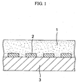
- Fig. 1 shows an example of a cross section of the surface of the molded component for the beam path of a radar apparatus according to the present invention.
- a base body 1 comprising a transparent resin layer
- a bright decoration layer 2 comprising tin and/or a tin alloy is disposed using a deposition method, for example, and a non-transparent resin layer 3 for enhancing the tone of color is formed.
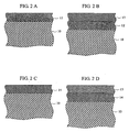
- Fig. 2 shows another example of a cross section of the surface of the molded component for the beam path of a radar apparatus according to the present invention.
- Fig. 2A shows a second example of the present invention.
- the molded component of the example comprises a base body 10 and a bright decoration layer 12 disposed thereon, the bright decoration layer being composed of tin.
- Fig. 2B shows a third example of the present invention.
- the bright decoration layer has a multilayered structure.
- the molded component comprises a base body 10, a first bright decoration layer 12 composed of tin disposed thereon, and a second bright decoration layer 13 composed of tin and/or a tin alloy disposed thereon.
- a multilayered structure for the bright decoration layer an appearance that shows a metallic color and a rainbow-like interference color can be obtained.
- Fig. 2C shows a fourth example of the present invention.
- the molded component of the example comprises a base body 10 and a bright decoration layer 14 composed of a tin alloy disposed thereon.
- Fig. 2D shows a fifth example of the present invention.
- the molded component of the example comprises a base body 10, a first bright decoration layer 14 composed of a tin alloy disposed thereon, and a second bright decoration layer 15 composed of tin disposed thereon.
- the bright decoration layers 12 and 15 composed of tin, and bright decoration layers 13 and 14 composed of a tin alloy, may be formed by a vacuum deposition method.
- each layer used to form the bright decoration layer has a thickness of 1 nm to 500 nm. Further preferably, the thickness is 10 nm to 100 nm.
- a desired color can be expressed by suitably selecting the material types that constitute the bright decoration layers 12 and 15 composed of tin, and bright decoration layers 13 and 14 composed of a tin alloy, and by suitably selecting the thickness of the layers.
- the base body 10 is composed of a material that is provides low radio transmission loss and is superior in terms of dielectric properties. Relative permittivity ⁇ ' and dielectric loss tan ⁇ , for example, provide an indication of the dielectric property.
- the base body 10 is composed of a transparent resin, preferably polycarbonate.
- a test piece composed of a polycarbonate film base body (base) whose thickness was 3.5 mm was prepared (comparative example 1).
- Bright film pieces were obtained by vacuum depositing tin on the polycarbonate film base bodies whose thicknesses were 3.5 mm such that the thicknesses of tin were 10 nm, 30 nm, and 50 nm (example).
- Bright film pieces were obtained by vacuum depositing indium instead of tin such that the thicknesses of indium were 10 nm, 30 nm, and 50 nm (comparative example 2).
- the tin-deposit pieces in the example had an appearance featuring a bright-silver effect that was equivalent to that of the indium-deposit pieces in comparative example 2.
- Table 1 shows these test pieces.
- Materials Film-forming method Film thickness Appearance Comparative example 1 Polycarbonate t 3.5 Transparent Example Polycarbonate t 3.5 Tin Vacuum deposition 10 nm Bright silver effect with slight transparency 30 nm Bright silver effect 50 nm Bright silver effect Comparative example 2
- radio transmission loss was measured at 76 GHz, which was frequency applied to millimeter-wave radars for automobiles.
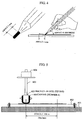
- Fig. 4 shows a pencil-scratch test method. As shown by the figure, the surface of a bright film was scratched using a pencil whose lead length was about 3 mm. The pencil was moved forward as much as 1 cm at a constant speed such that the angle of inclination of the pencil was about 45 degrees, the pencil being grabbed by a right hand and pressed as hard as possible onto the surface of the bright film without breaking the lead. Pencils with hardness ranging from high to low were used and the darkness scale of the pencils that caused exfoliation of the bright film was recorded. The evaluation was carried out on the basis of 9H in the darkness scale for the hardest pencil and 6B in the darkness scale for the softest pencil.
- FIG. 5 shows a plane abrasion test method.
- a sample 802 was fixed on a sample stage 801 and the surface of the sample 802 was rubbed by a friction block 803.
- a weight 806 was disposed on the friction block 803 via a support 805. Force provided to the tip of the friction block 803 was 9.8 N.
- the radius of a sphere at the tip of the friction block 803 was 10 mm and the surface thereof was covered with canvas (number 6) 804.
- the stroke width of the friction block 803 was 100 mm and the movement speed was 50 strokes per minute.
- the number of strokes was measured when the film on the surface of the sample started to experience exfoliation. The exfoliation of the film was determined by visual observation.
- Table 2 shows the measurement results.
- Example 10 0.5 30 0.7 Exfoliation by HB, no exfoliation by B Exfoliation at 40 to 50 strokes 50 0.8
- Comparative example 2 10 0.7 30 0.8 Exfoliation by 5B, no exfoliation by 6B Exfoliation at 3 to 5 strokes 50 0.8
- a tin-film component according to the present invention obtains a design featuring bright-silver effect equivalent to that of an indium-film component of the prior art and performance of millimeter-wave transmission loss, and provides a strong film layer that overcomes the problems of the indium-film component. Therefore, the component can be provided by a simpler material arrangement than in the case of a bright decoration component composed of the indium-film component of the prior art. The simpler material arrangement leads to productivity improvement, and materials can be obtained at a low price. Also, by using low-price tin materials, components can be provided at a low price, since indium-film components are considerably expensive.
- the molded component for the beam path of a radar apparatus with low radio transmission loss and improved hardness and abrasion resistance comprises a base body 1 composed of a resin layer, and a bright decoration layer 2 disposed on the surface of the base body, the bright decoration layer being composed of tin and/or a tin alloy.
Landscapes
- Engineering & Computer Science (AREA)
- Remote Sensing (AREA)
- Radar, Positioning & Navigation (AREA)
- Computer Security & Cryptography (AREA)
- Mechanical Engineering (AREA)
- Computer Networks & Wireless Communication (AREA)
- Physics & Mathematics (AREA)
- General Physics & Mathematics (AREA)
- Radar Systems Or Details Thereof (AREA)
- Support Of Aerials (AREA)
- Waveguide Connection Structure (AREA)
- Details Of Aerials (AREA)
Abstract
Description
- The present invention relates to a molded component for protecting a radar apparatus, especially to a molded component for the beam path of a radar apparatus disposed behind the front grill of an automobile.
- In general, antennas that transmit and receive radio waves in communication devices, radar devices, and the like have rarely been restricted in terms of the design of their bodies and peripheral structures, since their functions have been given priority. For example, a rod antenna whose shape is exposed is used for automobile radio antennas and the like. There may be a case where the antenna is hopefully hidden depending on the location in which the antenna is attached. For example, in a radar system or the like that measures obstacles in front of an automobile and the distance between automobiles, the antenna is preferably disposed in a central position at the front of the automobile in order to make the most of its performance. In this case, although the antenna is likely to be installed near the front grill of automobile, it is preferable that it not be possible to view the antenna from the outside in terms of design.
- An auto cruise system involves technology for controlling the distance between vehicles by accelerating or decelerating one's own vehicle, in which a sensor mounted in the front of the vehicle measures the distance and a relative speed between a vehicle in front and one's own vehicle, and the throttle and brakes are controlled based on this information. The auto cruise system has recently attracted attention as one of the core technologies of the intelligent transportation system (ITS) for easing traffic congestion and decreasing traffic accidents. In general, a radio transmitter-receiver device such as a millimeter-wave radar is used as a sensor for the auto cruise system.
- As shown in Fig. 6, a
radar apparatus 100 mounted in an automobile is usually disposed behind afront grill 101. Anemblem 102 of an automobile manufacturer or a specific decoration is disposed on thefront grill 101. Millimeter waves from the radar apparatus are radiated forward via the front grill and the emblem, and reflections from an object return to the radar apparatus via the front grill and the emblem. - Therefore, it is preferable to use materials and paints that provide low radio transmission loss and a predetermined appearance for the front grill and the emblem, especially where the beam path of a radar apparatus is arrayed.
- In this manner, a radio transmitter-receiver device is generally disposed behind the back surface of the front grill of a vehicle. However, there are many cases where the front grill is metal plated, so that it is difficult to transmit radio waves satisfactorily through the highly conductive metal. Also, front grills have a structure where air holes for taking in air are disposed, and front grills do not have uniform thicknesses. Therefore, when radio waves pass in and out through such a front grill, there is a difference in a radio transmission speed between the thin portion and the thick portion of the front grill, so that it is difficult to obtain good radar sensitivity.
- On account of these reasons, in general, a window portion that is capable of transmitting radio waves is disposed in a portion of the front grill that corresponds to the portion where the radio transmitter-receiver device is disposed. When the window portion is disposed in the front grill, radio waves can pass in and out through the window portion. However, by including a window portion, the appearance of the front grill loses continuity and the appearance of the vehicle may be spoiled, since the internal portions of the vehicle, such as the radio transmitter-receiver device and the engine area, are viewed.
- Therefore, conventionally, unity is provided between the window portion and the front grill body by inserting a radio transmission cover as disclosed in JP Patent Publication (Kokai) No. 2000-159039 A into the window portion of the front grill, for example. The radio transmission cover as disclosed in JP Patent Publication (Kokai) No. 2000-159039 A is formed by laminating a plurality of resin layers formed with concavity and convexity. This covering component can provide an impression by a metal layer deposited with concavity and convexity between the resin layers such that the fin member of the front grill continuously exists in the radio transmission cover.
- Indium is used as a metal deposited in such a radio transmission cover. When depositing indium on a deposit member, indium is not deposited on the surface of the deposit member in a uniform film manner, but deposited in a minute insular manner. In other words, when indium is deposited on the deposit member, the surface of the deposit member has a minute mixture of a deposit portion where indium is deposited in a minute insular manner and a non-deposit portion where nothing is deposited. In this case, radio waves can pass in and out through the non-deposit portion and the surface of the deposit member can be recognized upon viewing as a member that has metallic luster, since the deposit portion has indium deposited in a minute insular manner.
- However, as indium is an expensive metallic material, the increased material cost when the deposition is performed using indium is problematic. Moreover, it is difficult to form the deposited portion and the non-deposited portion in a well-balanced manner. For example, there is a case where radio waves do not pass in and out satisfactorily when the deposit portions are formed extremely closely together.
- JP Patent Publication (Kokai) No. 2003-252137A discloses a method for manufacturing a radio transmission cover in order to enable processing of a metallic film using various metallic materials in addition to indium, and to provide a method for manufacturing a radio transmission cover in which radio waves pass in and out satisfactorily. The method comprises a first step for forming a cover base member in a planar table manner, a second step for forming the metallic film on one surface of the cover base member such that the shape of the metallic film corresponds to the shape of the aforementioned fin portion, a third step for forming a bright portion in an insular manner by physically or chemically removing a part of the metallic film, and a fourth step for forming a transparent resin layer on the upper layer of a plane where the bright portion of the cover base member is formed. The radio transmission cover is disposed on the front grill of a vehicle, the front grill having a reticular fin portion, and a radio transmitter-receiver device is disposed on the back surface side thereof.
- JP Patent Publication (Kokai) No. 2000-159039 A and JP Patent Publication (Kokai) No. 2000-49522 A disclose a thin metallic layer comprising indium deposited on a metal portion area that can be viewed from the outside at a plastic-plated member for the beam path of a radar apparatus. However, it is necessary to ensure a bright design and the reliability of durability for radio transmittance by forming a stable protective layer so as not to allow the indium bright film layer to undergo exfoliation or be damaged by an external force, or to be corroded by an external environmental stress such as water or polluted air.
- This is due to the following facts: indium is a very soft metallic material with a value of 1.2 in the Mohs hardness scale; indium corrodes under the aforementioned environmental stress since it is basically a metallic material; it is necessary to ensure the reliability of durability by securing the film thickness with certainty such that the bright-effect design of indium can be obtained without thickening the indium film layer more than is necessary since a radio transmission loss occurs as a conductivity loss based on the fact that indium is basically a metallic material; and the indium layer melts due to the heat of molten resin when successively conducting secondary formation of the lining resin on a resin-molded component in which a film is formed on the surface of a base body in advance, since the melting point of indium is 156 °C, which is extremely low, for example.
- JP Patent Publication (Kokai) No. 2000-344032 A discloses a ceramic film comprising silicon dioxide disposed as a protective layer for preventing exfoliation and ensuring anticorrosion of an indium film.
- Although indium film is suitable for a film of an emblem or the like as it shows a metallic color, it poses problems in that it readily experiences exfoliation and lacks durability and abrasion resistance. Also, indium film may corrode, since it is basically a metal. Thus, when a ceramic film comprising silicon dioxide is disposed, the durability is improved and the film, or a paint, can be protected. However, the ceramic film comprising silicon dioxide is colorless, so that the appearance of a metallic color, for example, cannot be provided.
- In view of the aforementioned problems in the prior art, it is an object of the present invention to provide a molded component that offers stable effects as a product over a long period of time, which is a molded component providing a low level of radio transmission loss for the beam path of a radar apparatus. It is also an object of the present invention to provide a molded component that shows a bright color for the beam path of a radar apparatus.
- The inventors found that the aforementioned object could be achieved by using a specific metal for a bright decoration layer and arrived at the present invention.
- The present invention is an invention of a molded component for the beam path of a radar apparatus. The molded component comprises a base body composed of a resin layer, and a bright decoration layer on the surface of the base body, the bright decoration layer being composed of tin and/or a tin alloy. By using the bright decoration layer composed of tin and/or a tin alloy, hardness and abrasion resistance can be improved as compared with the indium layer of the prior art. Also, radio transmittance can be improved as compared with the indium layer.
- Preferably, the aforementioned tin and/or a tin alloy is tin (Sn) alone or an alloy of tin (Sn) and one or more elements selected from indium (In), gallium (Ga), antimony (Sb), and bismuth (Bi).
- The bright decoration layer comprising the aforementioned tin and/or a tin alloy can include a plurality of layers. For example, the bright decoration layer comprising the aforementioned tin and/or a tin alloy can include an Sn-alone layer and an Sn-alloy layer.
- Methods for forming the bright decoration layer comprising the aforementioned tin and/or a tin alloy are not limited. Specifically, methods include vacuum film forming methods such as a vacuum deposition method, an ion plating method, and a sputtering method, for example; vapor growth methods such as thermal CVD, plasma CVD, photo CVD, and MOCVD, for example; the LB (Langmuir-Blodgett) method, electroless deposition, the sol-gel method; and the like.
- Preferably, each layer that forms the bright decoration layer comprising the aforementioned tin and/or tin alloy has a thickness of 1 nm to 500 nm. Further preferably, the thickness is 10 nm to 100 nm.
- Preferably, the aforementioned base body is formed by a transparent resin that resulting in low radio transmission loss or a transparent resin resulting in low dielectric loss.
- The molded component for the beam path of a radar apparatus according to the present invention can further include a non-transparent resin layer for enhancing the tone of color.
- According to the present invention, a molded component for the beam path of a radar apparatus with low radio transmission loss and improved hardness and abrasion resistance can be provided.
-
- Fig. 1 shows a cross section of the surface area of the molded component for the beam path of a radar apparatus according to the present invention.
- Fig. 2 shows another cross section of the surface area of the molded component for the beam path of a radar apparatus according to the present invention.
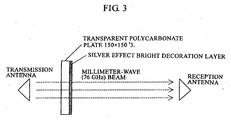
- Fig. 3 shows an illustration describing a test method of radio properties.
- Fig. 4 shows an illustration of a test method of hardness.
- Fig. 5 shows an illustration of a test method of abrasion resistance.
- Fig. 6 shows a conceptual diagram of an automobile on which a radar apparatus is disposed.
-
- Fig. 1 shows an example of a cross section of the surface of the molded component for the beam path of a radar apparatus according to the present invention. On the surface of a
base body 1 comprising a transparent resin layer, abright decoration layer 2 comprising tin and/or a tin alloy is disposed using a deposition method, for example, and anon-transparent resin layer 3 for enhancing the tone of color is formed. - Fig. 2 shows another example of a cross section of the surface of the molded component for the beam path of a radar apparatus according to the present invention. Fig. 2A shows a second example of the present invention. The molded component of the example comprises a
base body 10 and abright decoration layer 12 disposed thereon, the bright decoration layer being composed of tin. - Fig. 2B shows a third example of the present invention. In the molded component of the example, the bright decoration layer has a multilayered structure. The molded component comprises a
base body 10, a firstbright decoration layer 12 composed of tin disposed thereon, and a secondbright decoration layer 13 composed of tin and/or a tin alloy disposed thereon. By employing a multilayered structure for the bright decoration layer, an appearance that shows a metallic color and a rainbow-like interference color can be obtained. - Fig. 2C shows a fourth example of the present invention. The molded component of the example comprises a
base body 10 and abright decoration layer 14 composed of a tin alloy disposed thereon. Fig. 2D shows a fifth example of the present invention. The molded component of the example comprises abase body 10, a firstbright decoration layer 14 composed of a tin alloy disposed thereon, and a secondbright decoration layer 15 composed of tin disposed thereon. - The bright decoration layers 12 and 15 composed of tin, and bright decoration layers 13 and 14 composed of a tin alloy, may be formed by a vacuum deposition method. Preferably, each layer used to form the bright decoration layer has a thickness of 1 nm to 500 nm. Further preferably, the thickness is 10 nm to 100 nm.
- A desired color can be expressed by suitably selecting the material types that constitute the bright decoration layers 12 and 15 composed of tin, and bright decoration layers 13 and 14 composed of a tin alloy, and by suitably selecting the thickness of the layers.
- The
base body 10 is composed of a material that is provides low radio transmission loss and is superior in terms of dielectric properties. Relative permittivity ε' and dielectric loss tan δ, for example, provide an indication of the dielectric property. Thebase body 10 is composed of a transparent resin, preferably polycarbonate. - In the following, an example and comparative examples of the present invention are described.
- A test piece composed of a polycarbonate film base body (base) whose thickness was 3.5 mm was prepared (comparative example 1). Bright film pieces were obtained by vacuum depositing tin on the polycarbonate film base bodies whose thicknesses were 3.5 mm such that the thicknesses of tin were 10 nm, 30 nm, and 50 nm (example). Bright film pieces were obtained by vacuum depositing indium instead of tin such that the thicknesses of indium were 10 nm, 30 nm, and 50 nm (comparative example 2). The tin-deposit pieces in the example had an appearance featuring a bright-silver effect that was equivalent to that of the indium-deposit pieces in comparative example 2.
- Table 1 shows these test pieces.
Materials Film-forming method Film thickness Appearance Comparative example 1 Polycarbonate t 3.5 Transparent Example Polycarbonate t 3.5 Tin Vacuum deposition 10 nm Bright silver effect with slight transparency 30 nm Bright silver effect 50 nm Bright silver effect Comparative example 2 Polycarbonate t 3.5 Indium Vacuum deposition 10 nm Bright silver effect with slight transparency 30 nm Bright silver effect 50 nm Bright silver effect - As shown in Fig. 3, radio transmission loss was measured at 76 GHz, which was frequency applied to millimeter-wave radars for automobiles.
- A hardness test carried out by the inventors is described with reference to Fig. 4. Fig. 4 shows a pencil-scratch test method. As shown by the figure, the surface of a bright film was scratched using a pencil whose lead length was about 3 mm. The pencil was moved forward as much as 1 cm at a constant speed such that the angle of inclination of the pencil was about 45 degrees, the pencil being grabbed by a right hand and pressed as hard as possible onto the surface of the bright film without breaking the lead. Pencils with hardness ranging from high to low were used and the darkness scale of the pencils that caused exfoliation of the bright film was recorded.
The evaluation was carried out on the basis of 9H in the darkness scale for the hardest pencil and 6B in the darkness scale for the softest pencil. - An abrasion resistance test carried out by the inventors is described with reference to Fig. 5. Fig. 5 shows a plane abrasion test method. As shown by the figure, a
sample 802 was fixed on asample stage 801 and the surface of thesample 802 was rubbed by afriction block 803. Aweight 806 was disposed on thefriction block 803 via asupport 805. Force provided to the tip of thefriction block 803 was 9.8 N. The radius of a sphere at the tip of thefriction block 803 was 10 mm and the surface thereof was covered with canvas (number 6) 804. - The stroke width of the
friction block 803 was 100 mm and the movement speed was 50 strokes per minute. The number of strokes was measured when the film on the surface of the sample started to experience exfoliation. The exfoliation of the film was determined by visual observation. - Table 2 shows the measurement results.
Bright layer thickness (nm) Film component performance Millimeter-wave transmission loss Pencil hardness Abrasion resistance Example 10 0.5 30 0.7 Exfoliation by HB, no exfoliation by B Exfoliation at 40 to 50 strokes 50 0.8 Comparative example 2 10 0.7 30 0.8 Exfoliation by 5B, no exfoliation by 6B Exfoliation at 3 to 5 strokes 50 0.8 - As Table 2 indicates, a tin-film component according to the present invention obtains a design featuring bright-silver effect equivalent to that of an indium-film component of the prior art and performance of millimeter-wave transmission loss, and provides a strong film layer that overcomes the problems of the indium-film component. Therefore, the component can be provided by a simpler material arrangement than in the case of a bright decoration component composed of the indium-film component of the prior art. The simpler material arrangement leads to productivity improvement, and materials can be obtained at a low price. Also, by using low-price tin materials, components can be provided at a low price, since indium-film components are considerably expensive.
- A molded component for the beam path of a radar apparatus with low radio transmission loss and improved hardness and abrasion resistance is provided. The molded component for the beam path of the radar apparatus comprises a
base body 1 composed of a resin layer, and abright decoration layer 2 disposed on the surface of the base body, the bright decoration layer being composed of tin and/or a tin alloy.
Claims (10)
- A molded component for the beam path of a radar apparatus, comprising a base body composed of a resin layer, and a bright decoration layer disposed on the surface of said base body, said bright decoration layer comprising tin and/or a tin alloy.
- The molded component for the beam path of a radar apparatus according to claim 1, wherein the tin and/or a tin alloy comprises tin (Sn) alone or an alloy of tin (Sn) and one or more elements selected from indium (In), gallium (Ga), antimony (Sb), and bismuth (Bi).
- The molded component for the beam path of a radar apparatus according to claim 1 or 2, wherein said bright decoration layer comprising the tin and/or a tin alloy includes a plurality of layers.
- The molded component for the beam path of a radar apparatus according to any one of claims 1 to 3, wherein said bright decoration layer comprising the tin and/or a tin alloy includes an Sn-alone layer and an Sn-alloy layer.
- The molded component for the beam path of a radar apparatus according to any one of claims 1 to 4, wherein said bright decoration layer comprising the tin and/or a tin alloy is formed by vacuum deposition.
- The molded component for the beam path of a radar apparatus according to any one of claims 1 to 5, wherein each layer that forms said bright decoration layer comprising the tin and/or a tin alloy has a thickness of 1 nm to 500 nm.
- The molded component for the beam path of a radar apparatus according to any one of claims 1 to 5, wherein each layer that forms said bright decoration layer comprising the tin and/or a tin alloy has a thickness of 10 nm to 100 nm.
- The molded component for the beam path of a radar apparatus according to any one of claims 1 to 7, wherein said base body is formed by a transparent resin resulting in low radio transmission loss.
- The molded component for the beam path of a radar apparatus according to any one of claims 1 to 7, wherein said base body is formed by a transparent resin resulting in low dielectric loss.
- The molded component for the beam path of a radar apparatus according to any one of claims 1 to 9, further comprising a non-transparent resin layer for enhancing tone of color.
Applications Claiming Priority (2)
| Application Number | Priority Date | Filing Date | Title |
|---|---|---|---|
| JP2004025793 | 2004-02-02 | ||
| JP2004025793A JP2005212745A (en) | 2004-02-02 | 2004-02-02 | Molded product for use in radar device beam passage |
Publications (3)
| Publication Number | Publication Date |
|---|---|
| EP1560288A2 true EP1560288A2 (en) | 2005-08-03 |
| EP1560288A3 EP1560288A3 (en) | 2006-03-01 |
| EP1560288B1 EP1560288B1 (en) | 2008-07-23 |
Family
ID=34650890
Family Applications (1)
| Application Number | Title | Priority Date | Filing Date |
|---|---|---|---|
| EP05001731A Expired - Fee Related EP1560288B1 (en) | 2004-02-02 | 2005-01-27 | Molded component for beam path of radar apparatus |
Country Status (5)
| Country | Link |
|---|---|
| US (1) | US7468704B2 (en) |
| EP (1) | EP1560288B1 (en) |
| JP (1) | JP2005212745A (en) |
| CN (1) | CN100550514C (en) |
| DE (1) | DE602005008288D1 (en) |
Cited By (9)
| Publication number | Priority date | Publication date | Assignee | Title |
|---|---|---|---|---|
| EP1705749A1 (en) * | 2005-03-25 | 2006-09-27 | Toyota Jidosha Kabushiki Kaisha | Molded article for use in the beam path of a radar device |
| WO2012066417A1 (en) | 2010-11-15 | 2012-05-24 | Zanini Auto Grup, Sa | Decorative radome for automotive vehicular applications |
| WO2018010762A1 (en) | 2016-07-11 | 2018-01-18 | Zanini Auto Grup, S.A. | Radome for vehicles |
| EP3425730A1 (en) | 2017-07-05 | 2019-01-09 | Zanini Auto Grup, S.A. | Radome for vehicles |
| WO2020078916A2 (en) | 2018-10-15 | 2020-04-23 | Motherson Innovations Company Ltd. | Decorative radome and method of producing the same |
| WO2021018422A1 (en) | 2019-07-29 | 2021-02-04 | Motherson Innovations Company Ltd. | First surface or second surface decorative radome |
| FR3105608A1 (en) * | 2019-12-24 | 2021-06-25 | Compagnie Plastic Omnium Se | Motor vehicle radome comprising a decorative pattern |
| EP4142048A2 (en) | 2021-08-30 | 2023-03-01 | Motherson Innovations Company Ltd. | Decorative pvd coated items and radomes and methods of making same |
| US11827158B2 (en) | 2016-06-09 | 2023-11-28 | Zanini Auto Grup, S.A. | Radome for vehicles |
Families Citing this family (22)
| Publication number | Priority date | Publication date | Assignee | Title |
|---|---|---|---|---|
| JP2005212745A (en) * | 2004-02-02 | 2005-08-11 | Toyota Motor Corp | Molded product for use in radar device beam passage |
| JP2005249773A (en) * | 2004-02-02 | 2005-09-15 | Toyota Motor Corp | Molding for inside of beam path in radar system |
| JP2006005515A (en) * | 2004-06-16 | 2006-01-05 | Altia Hashimoto Co Ltd | Transparent device for radio wave or the like |
| JP4657070B2 (en) * | 2005-09-27 | 2011-03-23 | 豊田合成株式会社 | Radar device cover and manufacturing method thereof |
| JP2007130876A (en) * | 2005-11-10 | 2007-05-31 | Toyoda Gosei Co Ltd | Transparent ornament |
| JP2007240358A (en) * | 2006-03-09 | 2007-09-20 | Honda Motor Co Ltd | Exterior component for vehicle |
| JP2008080712A (en) * | 2006-09-28 | 2008-04-10 | Toyoda Gosei Co Ltd | Resin product which has metal film having brightness and discontinuous structure |
| US20110236672A1 (en) | 2008-12-01 | 2011-09-29 | Toyota Jidosha Kabushiki Kaisha | Decorative film and method for forming the same |
| JP4881984B2 (en) * | 2009-08-28 | 2012-02-22 | 株式会社ファルテック | Manufacturing method of radome |
| JP5747708B2 (en) * | 2011-07-21 | 2015-07-15 | トヨタ自動車株式会社 | Decorative coating |
| DE102011122346A1 (en) * | 2011-12-23 | 2013-06-27 | Valeo Schalter Und Sensoren Gmbh | Radar device for a motor vehicle, holder for a radar device and method for producing an absorption element for a radar device |
| JP2014145678A (en) * | 2013-01-29 | 2014-08-14 | Toyota Motor Corp | Decorative film |
| DE102013221055A1 (en) * | 2013-10-17 | 2015-04-23 | Robert Bosch Gmbh | Combination of radar sensor and cowling for a motor vehicle |
| JP6450671B2 (en) * | 2015-11-16 | 2019-01-09 | 豊田合成株式会社 | Decorative body and manufacturing method thereof |
| JP6872336B2 (en) * | 2016-09-27 | 2021-05-19 | 株式会社ファルテック | Radar cover |
| WO2018105644A1 (en) * | 2016-12-09 | 2018-06-14 | 株式会社ファルテック | Radar cover and manufacturing method for radar cover |
| WO2019064330A1 (en) * | 2017-09-26 | 2019-04-04 | 河西工業株式会社 | Exterior decorative component and method for manufacturing exterior decorative component |
| JP2020067291A (en) * | 2018-10-22 | 2020-04-30 | 豊田合成株式会社 | On-vehicle sensor cover |
| EP3956943A1 (en) | 2019-04-18 | 2022-02-23 | SRG Global, LLC | Stepped radar cover and method of manufacture |
| US20220276377A1 (en) * | 2019-07-05 | 2022-09-01 | Nitto Denko Corporation | Antireflection material and use thereof |
| JP7131506B2 (en) * | 2019-08-13 | 2022-09-06 | 豊田合成株式会社 | In-vehicle sensor cover |
| DE102021203582A1 (en) * | 2021-04-12 | 2022-10-13 | Magna Exteriors Gmbh | Method for manufacturing components of an outer skin of a vehicle |
Citations (5)
| Publication number | Priority date | Publication date | Assignee | Title |
|---|---|---|---|---|
| US3396400A (en) * | 1965-03-30 | 1968-08-06 | Goodyear Aerospace Corp | Radar transparent covering |
| US4241129A (en) * | 1978-12-15 | 1980-12-23 | The Dow Chemical Company | Delamination resistant multilayer metal/polymer composites |
| US6184842B1 (en) * | 1998-05-02 | 2001-02-06 | Daimlerchrysler | Process for manufacturing a radome for a range warning radar |
| US6328358B1 (en) * | 1998-09-24 | 2001-12-11 | Daimlerchrysler Ag | Cover part located within the beam path of a radar |
| US20020171579A1 (en) * | 2001-04-20 | 2002-11-21 | Thales | Vehicle radar concealment device bearing a pattern, and method for making such a device |
Family Cites Families (38)
| Publication number | Priority date | Publication date | Assignee | Title |
|---|---|---|---|---|
| US3154432A (en) * | 1961-06-15 | 1964-10-27 | Gen Electric | Coated polycarbonate resin recording sheet |
| US3255035A (en) * | 1961-11-15 | 1966-06-07 | Nat Res Corp | Tin oxide coating |
| US4419570A (en) * | 1980-03-03 | 1983-12-06 | Societa Italiana Vetro - Siv - S.P.A. | Heating glass pane |
| US4837135A (en) * | 1987-08-13 | 1989-06-06 | E. I. Du Pont De Nemours And Company | Electron beam recording film |
| KR930011749B1 (en) * | 1989-11-15 | 1993-12-20 | 신닛뽄세이테쓰 가부시키가이샤 | Resin coated steel for draw wiping can and draw wiping can |
| DE69427506T2 (en) * | 1993-08-20 | 2001-10-04 | Asahi Glass Co Ltd | Window antenna for an automobile |
| JPH08103982A (en) * | 1994-10-05 | 1996-04-23 | Dainippon Printing Co Ltd | Lustrous decorative sheet |
| US5911899A (en) * | 1995-06-15 | 1999-06-15 | Mitsui Chemicals, Inc. | Corrosion-proof transparent heater panels and preparation process thereof |
| US6224976B1 (en) * | 1996-08-14 | 2001-05-01 | Asahi Kogaku Kogyo Kabushiki Kaisha | Adhesive transparent resin and a composite including the same |
| JPH1081837A (en) * | 1996-09-05 | 1998-03-31 | Nisshin Steel Co Ltd | High-weather-resistant metallic pigment |
| JP4672818B2 (en) * | 1996-12-23 | 2011-04-20 | ノボ ノルディスク アクティーゼルスカブ | Drug container made of linear olefin polymer for storing liquid drug |
| JPH10193549A (en) * | 1997-01-08 | 1998-07-28 | Hashimoto Forming Ind Co Ltd | Decoration trim exhibiting metallic lustrous color, its manufacture and laminated film used for the method |
| JP3243789B2 (en) * | 1997-03-31 | 2002-01-07 | 日本板硝子株式会社 | Radio wave absorbing panel |
| JPH10278582A (en) * | 1997-04-07 | 1998-10-20 | Nitsusen Kagaku Kk | Visor for automobile |
| US6413630B1 (en) * | 1997-05-15 | 2002-07-02 | 3M Innovative Properties Company | Decorative film |
| CA2279737C (en) * | 1998-08-06 | 2004-04-27 | Naoya Haruta | Decorative film for use in platics molding, process for preparing the same and injection-molded part by use of the same |
| US6335479B1 (en) * | 1998-10-13 | 2002-01-01 | Dai Nippon Printing Co., Ltd. | Protective sheet for solar battery module, method of fabricating the same and solar battery module |
| JP3671126B2 (en) * | 1999-03-19 | 2005-07-13 | Tdk株式会社 | Optical information medium and manufacturing method thereof |
| JP2000344032A (en) | 1999-06-08 | 2000-12-12 | Nissan Motor Co Ltd | Grill cover structure |
| EP1072905A1 (en) * | 1999-07-22 | 2001-01-31 | Yasuhiro Koike | Refractive index distribution type light transmitting device |
| JP3646858B2 (en) * | 1999-08-09 | 2005-05-11 | 株式会社ジェイエスピー | MULTILAYER POLYPROPYLENE RESIN FOAM MOLDED BODY, PROCESS FOR PRODUCING THE SAME, AND CONTAINER |
| US6620493B2 (en) * | 2000-03-07 | 2003-09-16 | Fukuvi Chemcial Industry Co Ltd | Reflection-reducing film |
| TW525195B (en) * | 2000-03-28 | 2003-03-21 | Toyo Boseki | Transparent conductive film, transparent conductive sheet and touch panel |
| DE10026454C1 (en) * | 2000-05-27 | 2001-12-20 | Daimler Chrysler Ag | Radome for a distance warning radar (AWR) |
| US7314659B2 (en) * | 2000-07-21 | 2008-01-01 | Target Technology Company, Llc | Metal alloys for the reflective or semi-reflective layer of an optical storage medium |
| JP3755809B2 (en) * | 2000-10-27 | 2006-03-15 | 本田技研工業株式会社 | Radio wave permeable exterior part and manufacturing method thereof |
| JP4099946B2 (en) * | 2001-01-11 | 2008-06-11 | 株式会社ファルテック | Method for producing molded product exhibiting metallic brilliant color |
| JP4467816B2 (en) * | 2001-02-27 | 2010-05-26 | 株式会社日立製作所 | Low dielectric loss tangent resin composition, curable film, cured product, electrical component using the same, and production method thereof |
| US6465102B1 (en) * | 2001-03-22 | 2002-10-15 | General Electric Company | Formed decorative article |
| US6726964B1 (en) * | 2001-07-11 | 2004-04-27 | G. Alan Thompson | Ultrasonic process for autocatalytic deposition of metal on microparticulate |
| JP4006994B2 (en) * | 2001-12-18 | 2007-11-14 | 株式会社リコー | Three-dimensional structure processing method, three-dimensional product manufacturing method, and three-dimensional structure |
| JP3951740B2 (en) * | 2002-02-26 | 2007-08-01 | 豊田合成株式会社 | Manufacturing method of radio wave transmission cover |
| JP4022819B2 (en) * | 2002-12-26 | 2007-12-19 | 豊田合成株式会社 | Radio wave transmission cover |
| US20040174596A1 (en) * | 2003-03-05 | 2004-09-09 | Ricoh Optical Industries Co., Ltd. | Polarization optical device and manufacturing method therefor |
| JP2005041914A (en) * | 2003-07-23 | 2005-02-17 | Hitachi Ltd | Resin composition containing rubber component and film and electric part using the same |
| JP2005212745A (en) * | 2004-02-02 | 2005-08-11 | Toyota Motor Corp | Molded product for use in radar device beam passage |
| EP1688188B1 (en) * | 2005-02-02 | 2012-04-11 | Toyo Kohan Co., Ltd. | Metal plate coated with polyester resin, and can using the same |
| JP4667923B2 (en) * | 2005-03-25 | 2011-04-13 | トヨタ自動車株式会社 | Brightening molded parts for radar device beam path |
-
2004
- 2004-02-02 JP JP2004025793A patent/JP2005212745A/en active Pending
-
2005
- 2005-01-26 US US11/042,113 patent/US7468704B2/en not_active Expired - Fee Related
- 2005-01-27 DE DE602005008288T patent/DE602005008288D1/en active Active
- 2005-01-27 EP EP05001731A patent/EP1560288B1/en not_active Expired - Fee Related
- 2005-02-01 CN CNB2005100052384A patent/CN100550514C/en not_active Expired - Fee Related
Patent Citations (5)
| Publication number | Priority date | Publication date | Assignee | Title |
|---|---|---|---|---|
| US3396400A (en) * | 1965-03-30 | 1968-08-06 | Goodyear Aerospace Corp | Radar transparent covering |
| US4241129A (en) * | 1978-12-15 | 1980-12-23 | The Dow Chemical Company | Delamination resistant multilayer metal/polymer composites |
| US6184842B1 (en) * | 1998-05-02 | 2001-02-06 | Daimlerchrysler | Process for manufacturing a radome for a range warning radar |
| US6328358B1 (en) * | 1998-09-24 | 2001-12-11 | Daimlerchrysler Ag | Cover part located within the beam path of a radar |
| US20020171579A1 (en) * | 2001-04-20 | 2002-11-21 | Thales | Vehicle radar concealment device bearing a pattern, and method for making such a device |
Cited By (12)
| Publication number | Priority date | Publication date | Assignee | Title |
|---|---|---|---|---|
| EP1705749A1 (en) * | 2005-03-25 | 2006-09-27 | Toyota Jidosha Kabushiki Kaisha | Molded article for use in the beam path of a radar device |
| US7619575B2 (en) | 2005-03-25 | 2009-11-17 | Toyota Jidosha Kabushiki Kaisha | Metallically gross layer decorative molded article for use in the beam path of a radar device |
| WO2012066417A1 (en) | 2010-11-15 | 2012-05-24 | Zanini Auto Grup, Sa | Decorative radome for automotive vehicular applications |
| US9114760B2 (en) | 2010-11-15 | 2015-08-25 | Zanini Auto Grup, Sa | Decorative radome for automotive vehicular applications |
| US11827158B2 (en) | 2016-06-09 | 2023-11-28 | Zanini Auto Grup, S.A. | Radome for vehicles |
| WO2018010762A1 (en) | 2016-07-11 | 2018-01-18 | Zanini Auto Grup, S.A. | Radome for vehicles |
| EP3425730A1 (en) | 2017-07-05 | 2019-01-09 | Zanini Auto Grup, S.A. | Radome for vehicles |
| WO2020078916A2 (en) | 2018-10-15 | 2020-04-23 | Motherson Innovations Company Ltd. | Decorative radome and method of producing the same |
| WO2021018422A1 (en) | 2019-07-29 | 2021-02-04 | Motherson Innovations Company Ltd. | First surface or second surface decorative radome |
| FR3105608A1 (en) * | 2019-12-24 | 2021-06-25 | Compagnie Plastic Omnium Se | Motor vehicle radome comprising a decorative pattern |
| WO2021130295A1 (en) * | 2019-12-24 | 2021-07-01 | Compagnie Plastic Omnium Se | Radome for motor vehicle comprising a decorative pattern |
| EP4142048A2 (en) | 2021-08-30 | 2023-03-01 | Motherson Innovations Company Ltd. | Decorative pvd coated items and radomes and methods of making same |
Also Published As
| Publication number | Publication date |
|---|---|
| US20050168374A1 (en) | 2005-08-04 |
| EP1560288A3 (en) | 2006-03-01 |
| CN1652399A (en) | 2005-08-10 |
| JP2005212745A (en) | 2005-08-11 |
| CN100550514C (en) | 2009-10-14 |
| US7468704B2 (en) | 2008-12-23 |
| DE602005008288D1 (en) | 2008-09-04 |
| EP1560288B1 (en) | 2008-07-23 |
Similar Documents
| Publication | Publication Date | Title |
|---|---|---|
| US7468704B2 (en) | Molded component for beam path of radar apparatus | |
| US9114760B2 (en) | Decorative radome for automotive vehicular applications | |
| US7619575B2 (en) | Metallically gross layer decorative molded article for use in the beam path of a radar device | |
| CN106908884B (en) | Radio wave-transparent layer having metallic luster | |
| US7256746B2 (en) | Molded component for beam path of radar apparatus | |
| US11827158B2 (en) | Radome for vehicles | |
| US7824782B2 (en) | Molded article located in the beam path of radar device, and method of manufacturing the same | |
| US10873129B2 (en) | Radome for vehicles | |
| JP5210919B2 (en) | Vehicle exterior member and front grill | |
| US11128037B2 (en) | Radome for vehicles | |
| JP6671718B2 (en) | Method for producing millimeter-wave permeable resin member having metal film formed on resin substrate and millimeter wave permeable resin member | |
| CN112004666A (en) | Electromagnetic wave transmitting metallic luster article |
Legal Events
| Date | Code | Title | Description |
|---|---|---|---|
| PUAI | Public reference made under article 153(3) epc to a published international application that has entered the european phase |
Free format text: ORIGINAL CODE: 0009012 |
|
| 17P | Request for examination filed |
Effective date: 20050127 |
|
| AK | Designated contracting states |
Kind code of ref document: A2 Designated state(s): AT BE BG CH CY CZ DE DK EE ES FI FR GB GR HU IE IS IT LI LT LU MC NL PL PT RO SE SI SK TR |
|
| AX | Request for extension of the european patent |
Extension state: AL BA HR LV MK YU |
|
| PUAL | Search report despatched |
Free format text: ORIGINAL CODE: 0009013 |
|
| AK | Designated contracting states |
Kind code of ref document: A3 Designated state(s): AT BE BG CH CY CZ DE DK EE ES FI FR GB GR HU IE IS IT LI LT LU MC NL PL PT RO SE SI SK TR |
|
| AX | Request for extension of the european patent |
Extension state: AL BA HR LV MK YU |
|
| AKX | Designation fees paid |
Designated state(s): DE FR GB IT |
|
| GRAP | Despatch of communication of intention to grant a patent |
Free format text: ORIGINAL CODE: EPIDOSNIGR1 |
|
| GRAS | Grant fee paid |
Free format text: ORIGINAL CODE: EPIDOSNIGR3 |
|
| GRAA | (expected) grant |
Free format text: ORIGINAL CODE: 0009210 |
|
| AK | Designated contracting states |
Kind code of ref document: B1 Designated state(s): DE FR GB IT |
|
| REG | Reference to a national code |
Ref country code: GB Ref legal event code: FG4D |
|
| REF | Corresponds to: |
Ref document number: 602005008288 Country of ref document: DE Date of ref document: 20080904 Kind code of ref document: P |
|
| PLBE | No opposition filed within time limit |
Free format text: ORIGINAL CODE: 0009261 |
|
| STAA | Information on the status of an ep patent application or granted ep patent |
Free format text: STATUS: NO OPPOSITION FILED WITHIN TIME LIMIT |
|
| 26N | No opposition filed |
Effective date: 20090424 |
|
| PGFP | Annual fee paid to national office [announced via postgrant information from national office to epo] |
Ref country code: IT Payment date: 20120117 Year of fee payment: 8 |
|
| REG | Reference to a national code |
Ref country code: GB Ref legal event code: 746 Effective date: 20121012 |
|
| REG | Reference to a national code |
Ref country code: DE Ref legal event code: R084 Ref document number: 602005008288 Country of ref document: DE Effective date: 20121015 |
|
| PGFP | Annual fee paid to national office [announced via postgrant information from national office to epo] |
Ref country code: GB Payment date: 20130123 Year of fee payment: 9 Ref country code: FR Payment date: 20130204 Year of fee payment: 9 Ref country code: DE Payment date: 20130123 Year of fee payment: 9 |
|
| REG | Reference to a national code |
Ref country code: DE Ref legal event code: R119 Ref document number: 602005008288 Country of ref document: DE |
|
| GBPC | Gb: european patent ceased through non-payment of renewal fee |
Effective date: 20140127 |
|
| PG25 | Lapsed in a contracting state [announced via postgrant information from national office to epo] |
Ref country code: DE Free format text: LAPSE BECAUSE OF NON-PAYMENT OF DUE FEES Effective date: 20140801 |
|
| REG | Reference to a national code |
Ref country code: FR Ref legal event code: ST Effective date: 20140930 |
|
| REG | Reference to a national code |
Ref country code: DE Ref legal event code: R119 Ref document number: 602005008288 Country of ref document: DE Effective date: 20140801 |
|
| PG25 | Lapsed in a contracting state [announced via postgrant information from national office to epo] |
Ref country code: GB Free format text: LAPSE BECAUSE OF NON-PAYMENT OF DUE FEES Effective date: 20140127 Ref country code: FR Free format text: LAPSE BECAUSE OF NON-PAYMENT OF DUE FEES Effective date: 20140131 |
|
| PG25 | Lapsed in a contracting state [announced via postgrant information from national office to epo] |
Ref country code: IT Free format text: LAPSE BECAUSE OF NON-PAYMENT OF DUE FEES Effective date: 20140127 |