EP1557863A2 - Antistatic film, spacer using it and picture display unit - Google Patents
Antistatic film, spacer using it and picture display unit Download PDFInfo
- Publication number
- EP1557863A2 EP1557863A2 EP05001204A EP05001204A EP1557863A2 EP 1557863 A2 EP1557863 A2 EP 1557863A2 EP 05001204 A EP05001204 A EP 05001204A EP 05001204 A EP05001204 A EP 05001204A EP 1557863 A2 EP1557863 A2 EP 1557863A2
- Authority
- EP
- European Patent Office
- Prior art keywords
- film
- antistatic film
- aluminum
- nitride
- oxide
- Prior art date
- Legal status (The legal status is an assumption and is not a legal conclusion. Google has not performed a legal analysis and makes no representation as to the accuracy of the status listed.)
- Granted
Links
Images


Classifications
-
- C—CHEMISTRY; METALLURGY
- C23—COATING METALLIC MATERIAL; COATING MATERIAL WITH METALLIC MATERIAL; CHEMICAL SURFACE TREATMENT; DIFFUSION TREATMENT OF METALLIC MATERIAL; COATING BY VACUUM EVAPORATION, BY SPUTTERING, BY ION IMPLANTATION OR BY CHEMICAL VAPOUR DEPOSITION, IN GENERAL; INHIBITING CORROSION OF METALLIC MATERIAL OR INCRUSTATION IN GENERAL
- C23C—COATING METALLIC MATERIAL; COATING MATERIAL WITH METALLIC MATERIAL; SURFACE TREATMENT OF METALLIC MATERIAL BY DIFFUSION INTO THE SURFACE, BY CHEMICAL CONVERSION OR SUBSTITUTION; COATING BY VACUUM EVAPORATION, BY SPUTTERING, BY ION IMPLANTATION OR BY CHEMICAL VAPOUR DEPOSITION, IN GENERAL
- C23C14/00—Coating by vacuum evaporation, by sputtering or by ion implantation of the coating forming material
- C23C14/22—Coating by vacuum evaporation, by sputtering or by ion implantation of the coating forming material characterised by the process of coating
- C23C14/34—Sputtering
- C23C14/3407—Cathode assembly for sputtering apparatus, e.g. Target
- C23C14/3414—Metallurgical or chemical aspects of target preparation, e.g. casting, powder metallurgy
-
- H—ELECTRICITY
- H01—ELECTRIC ELEMENTS
- H01J—ELECTRIC DISCHARGE TUBES OR DISCHARGE LAMPS
- H01J31/00—Cathode ray tubes; Electron beam tubes
- H01J31/02—Cathode ray tubes; Electron beam tubes having one or more output electrodes which may be impacted selectively by the ray or beam, and onto, from, or over which the ray or beam may be deflected or de-focused
-
- C—CHEMISTRY; METALLURGY
- C09—DYES; PAINTS; POLISHES; NATURAL RESINS; ADHESIVES; COMPOSITIONS NOT OTHERWISE PROVIDED FOR; APPLICATIONS OF MATERIALS NOT OTHERWISE PROVIDED FOR
- C09K—MATERIALS FOR MISCELLANEOUS APPLICATIONS, NOT PROVIDED FOR ELSEWHERE
- C09K3/00—Materials not provided for elsewhere
- C09K3/16—Anti-static materials
-
- C—CHEMISTRY; METALLURGY
- C23—COATING METALLIC MATERIAL; COATING MATERIAL WITH METALLIC MATERIAL; CHEMICAL SURFACE TREATMENT; DIFFUSION TREATMENT OF METALLIC MATERIAL; COATING BY VACUUM EVAPORATION, BY SPUTTERING, BY ION IMPLANTATION OR BY CHEMICAL VAPOUR DEPOSITION, IN GENERAL; INHIBITING CORROSION OF METALLIC MATERIAL OR INCRUSTATION IN GENERAL
- C23C—COATING METALLIC MATERIAL; COATING MATERIAL WITH METALLIC MATERIAL; SURFACE TREATMENT OF METALLIC MATERIAL BY DIFFUSION INTO THE SURFACE, BY CHEMICAL CONVERSION OR SUBSTITUTION; COATING BY VACUUM EVAPORATION, BY SPUTTERING, BY ION IMPLANTATION OR BY CHEMICAL VAPOUR DEPOSITION, IN GENERAL
- C23C14/00—Coating by vacuum evaporation, by sputtering or by ion implantation of the coating forming material
- C23C14/0021—Reactive sputtering or evaporation
- C23C14/0036—Reactive sputtering
-
- C—CHEMISTRY; METALLURGY
- C23—COATING METALLIC MATERIAL; COATING MATERIAL WITH METALLIC MATERIAL; CHEMICAL SURFACE TREATMENT; DIFFUSION TREATMENT OF METALLIC MATERIAL; COATING BY VACUUM EVAPORATION, BY SPUTTERING, BY ION IMPLANTATION OR BY CHEMICAL VAPOUR DEPOSITION, IN GENERAL; INHIBITING CORROSION OF METALLIC MATERIAL OR INCRUSTATION IN GENERAL
- C23C—COATING METALLIC MATERIAL; COATING MATERIAL WITH METALLIC MATERIAL; SURFACE TREATMENT OF METALLIC MATERIAL BY DIFFUSION INTO THE SURFACE, BY CHEMICAL CONVERSION OR SUBSTITUTION; COATING BY VACUUM EVAPORATION, BY SPUTTERING, BY ION IMPLANTATION OR BY CHEMICAL VAPOUR DEPOSITION, IN GENERAL
- C23C14/00—Coating by vacuum evaporation, by sputtering or by ion implantation of the coating forming material
- C23C14/06—Coating by vacuum evaporation, by sputtering or by ion implantation of the coating forming material characterised by the coating material
- C23C14/0688—Cermets, e.g. mixtures of metal and one or more of carbides, nitrides, oxides or borides
-
- H—ELECTRICITY
- H01—ELECTRIC ELEMENTS
- H01J—ELECTRIC DISCHARGE TUBES OR DISCHARGE LAMPS
- H01J29/00—Details of cathode-ray tubes or of electron-beam tubes of the types covered by group H01J31/00
- H01J29/02—Electrodes; Screens; Mounting, supporting, spacing or insulating thereof
-
- H—ELECTRICITY
- H01—ELECTRIC ELEMENTS
- H01J—ELECTRIC DISCHARGE TUBES OR DISCHARGE LAMPS
- H01J29/00—Details of cathode-ray tubes or of electron-beam tubes of the types covered by group H01J31/00
- H01J29/02—Electrodes; Screens; Mounting, supporting, spacing or insulating thereof
- H01J29/028—Mounting or supporting arrangements for flat panel cathode ray tubes, e.g. spacers particularly relating to electrodes
-
- H—ELECTRICITY
- H01—ELECTRIC ELEMENTS
- H01J—ELECTRIC DISCHARGE TUBES OR DISCHARGE LAMPS
- H01J29/00—Details of cathode-ray tubes or of electron-beam tubes of the types covered by group H01J31/00
- H01J29/86—Vessels; Containers; Vacuum locks
- H01J29/864—Spacers between faceplate and backplate of flat panel cathode ray tubes
-
- H—ELECTRICITY
- H01—ELECTRIC ELEMENTS
- H01J—ELECTRIC DISCHARGE TUBES OR DISCHARGE LAMPS
- H01J9/00—Apparatus or processes specially adapted for the manufacture, installation, removal, maintenance of electric discharge tubes, discharge lamps, or parts thereof; Recovery of material from discharge tubes or lamps
- H01J9/24—Manufacture or joining of vessels, leading-in conductors or bases
- H01J9/241—Manufacture or joining of vessels, leading-in conductors or bases the vessel being for a flat panel display
- H01J9/242—Spacers between faceplate and backplate
-
- H—ELECTRICITY
- H01—ELECTRIC ELEMENTS
- H01J—ELECTRIC DISCHARGE TUBES OR DISCHARGE LAMPS
- H01J2329/00—Electron emission display panels, e.g. field emission display panels
- H01J2329/86—Vessels
- H01J2329/8625—Spacing members
- H01J2329/864—Spacing members characterised by the material
-
- H—ELECTRICITY
- H01—ELECTRIC ELEMENTS
- H01J—ELECTRIC DISCHARGE TUBES OR DISCHARGE LAMPS
- H01J2329/00—Electron emission display panels, e.g. field emission display panels
- H01J2329/86—Vessels
- H01J2329/8625—Spacing members
- H01J2329/8645—Spacing members with coatings on the lateral surfaces thereof
-
- H—ELECTRICITY
- H01—ELECTRIC ELEMENTS
- H01J—ELECTRIC DISCHARGE TUBES OR DISCHARGE LAMPS
- H01J2329/00—Electron emission display panels, e.g. field emission display panels
- H01J2329/86—Vessels
- H01J2329/8625—Spacing members
- H01J2329/865—Connection of the spacing members to the substrates or electrodes
- H01J2329/8655—Conductive or resistive layers
-
- Y—GENERAL TAGGING OF NEW TECHNOLOGICAL DEVELOPMENTS; GENERAL TAGGING OF CROSS-SECTIONAL TECHNOLOGIES SPANNING OVER SEVERAL SECTIONS OF THE IPC; TECHNICAL SUBJECTS COVERED BY FORMER USPC CROSS-REFERENCE ART COLLECTIONS [XRACs] AND DIGESTS
- Y10—TECHNICAL SUBJECTS COVERED BY FORMER USPC
- Y10T—TECHNICAL SUBJECTS COVERED BY FORMER US CLASSIFICATION
- Y10T428/00—Stock material or miscellaneous articles
- Y10T428/25—Web or sheet containing structurally defined element or component and including a second component containing structurally defined particles
Definitions
- the present invention relates to an antistatic film installed in an airtight vessel containing an electron source of an electron-generating device such as a picture display unit, to a spacer using it, and to the picture display unit.
- a flat display unit using an electron-emitting device has, as shown in Japanese Patent Application Laid-Open No. H10-284286, a spacer called as the spacer or a rib installed therein, which is a structural support resistant to ambient pressure for keeping the inside of the unit into a high vacuum.
- FIG. 7 is a cross-sectional schematic view of an image-forming apparatus using many electron-emitting devices.
- Reference numeral 101 denotes a rear plate
- reference numeral 102 a sidewall and reference numeral 103 a faceplate
- an airtight vessel is formed by the rear plate 101, the side wall 102 and the face plate 103.
- a spacer 107b that is a structural support resistant to ambient pressure in the airtight vessel has a low-resistivity film 110 thereon, and is connected to wiring 109 through an electroconductive frit 108.
- An electron-emitting device 104 is formed on a rear plate 101, and a phosphor 105 and a metal back 106 are formed on a face plate.
- Objects of providing a metal back 106 are to improve a utilization factor of light by mirror-reflecting a light emitted from a phosphor 105; to protect the phosphor 105 from the collision of negative ions; to work as an electrode for applying an electron beam-accelerating voltage; and to work as a conducting path for electrons after having excited the phosphor 105.
- a spacer 107a shows the electrostatically charged state of the spacer, and shows a state in which electrostatic charge (positive electrostatic charge in the drawing) is caused by collision of one part of electrons emitted from an electron source around it.
- the spacer 107a shows the electrostatically charged state of the spacer when having no antistatic film 112 installed thereon, and thus, the thickness of a low-resistivity film is drawn more thickly than the low-resistivity film 110 contacting with the antistatic film 112 of the spacer 107b, for convenience in illustration.
- Japanese Patent Application Laid-Open No. H10-284283 proposes a spacer coated with an electrostatic charge-mitigating film containing aluminum nitride or aluminum oxide, and noble metals such as gold, palladium and platinum, by binary simultaneous sputtering with the use of an aluminum target and a noble metal target, and of a mixed gas of argon and nitrogen or oxygen as a gas for forming a film.
- the distribution of resistivity is also formed due to the temperature characteristic of the resistivity of the antistatic film.
- the variation of resistivity leads to the variation in the diselectrification function.
- the instability of a display image results from temperature distribution in a panel plane, which is caused by a temperature difference between a face plate and a rear plate.
- a conventional method of forming an antistatic film containing a plurality of elements by sputtering simultaneously a plurality of different material targets might cause variation in the resistivity of an antistatic film depending on each film-forming batch even when film-forming conditions (background, sputtering pressure, gas flow rate and target electrification power) are uniformized.
- target electrification powers supplied to different material targets are required to be adjusted to each, which is complicated, and the operation is not always highly reproducible.
- cross contamination can not be avoided, which is a phenomenon that a more powerfully electrified target material deposits on the surface of a less powerfully electrified target material.
- An object of the present invention is to provide an antistatic film having superior controllability for a resistivity value, stability and reproducibility, and the adequate temperature characteristics of resistance.
- the present invention provides an antistatic film having a structure comprising a plurality of conductor particles with particle diameters of 0.5 to 10 nm dispersed in a medium containing a nitride.
- the present invention provides an antistatic film having a structure comprising a plurality of conductor particles with particle diameters of 0.5 to 10 nm dispersed in a medium containing an oxide.
- the present invention provides an antistatic film having a structure comprising a plurality of conductor particles with particle diameters of 0.5 to 10 nm dispersed in a medium containing a nitride and an oxide.
- the present invention provides an antistatic film having a structure comprising a plurality of semiconductor particles with particle diameters of 0.5 to 10 nm dispersed in a medium containing a nitride.
- the present invention provides an antistatic film having a structure comprising a plurality of semiconductor particles with particle diameters of 0.5 to 10 nm dispersed in a medium containing an oxide.
- the present invention provides an antistatic film having a structure of dispersing a plurality of semiconductive particles with particle diameters of 0.5 to 10 nm in a medium containing a nitride and an oxide.
- media which it was described above, it points at the part except for the particles which have the particle diameters of 0.5 to 10nm dispersed in a film and which exists.
- the present invention provides an electron-generating device with an electron source in an airtight vessel, comprising any of the above described antistatic films in the airtight vessel.
- the present invention provides a picture display unit provided with an airtight vessel having a first substrate with an electron source arranged thereon, and a second substrate with an image display member arranged thereon so as to face the electron source, and a spacer arranged between the first and second substrates in the above described airtight vessel, wherein the spacer has any of the above described antistatic films arranged on the surface.
- the present invention provides a spacer arranged between a first substrate and a second substrate in a picture display unit provided with an airtight vessel having the first substrate with an electron source arranged thereon and the second substrate having an image display member arranged thereon so as to face the electron source, wherein the spacer has any of the above described antistatic films on the surface.
- the present invention provides an antistatic film having a structure comprising a plurality of conductor particles with particle diameters of 0.5 to 10 nm dispersed in a medium containing a nitride.
- the present invention provides an antistatic film having a structure comprising a plurality of conductor particles with particle diameters of 0.5 to 10 nm dispersed in a medium containing an oxide.
- the present invention provides an antistatic film having a structure comprising a plurality of conductor particles with particle diameters of 0.5 to 10 nm dispersed in a medium containing a nitride and an oxide.
- the conductor particle is preferably a noble metal particle.
- the conductor particle is preferably a platinum particle
- the nitride is preferably aluminum nitride.
- the conductor particle is preferably a platinum particle, and the oxide is preferably aluminum oxide.
- the conductor particle is preferably a platinum particle
- a nitride is preferably aluminum nitride
- the oxide is preferably aluminum oxide.
- the conductor particle is preferably a gold particle
- the nitride is preferably aluminum nitride.
- the conductive particle is preferably a gold particle, and the oxide is preferably aluminum oxide.
- the conductor particle is preferably a gold particle
- the nitride is preferably aluminum nitride
- the oxide is preferably aluminum oxide.
- the conductor particle is preferably a silver particle
- the nitride is preferably aluminum nitride.
- the conductor particle is preferably a silver particle, and the oxide is preferably aluminum oxide.
- the conductor particle is preferably a silver particle
- the nitride is preferably aluminum nitride
- the oxide is preferably aluminum oxide.
- the content of the conductor is preferably 0.1 to 10 atomic%.
- the present invention provides an antistatic film having a structure comprising a plurality of semiconductor particles with particle diameters of 0.5 to 10 nm dispersed in a medium containing a nitride.
- the present invention provides an antistatic film having a structure comprising a plurality of semiconductor particles with particle diameters of 0.5 to 10 nm dispersed in a medium containing an oxide.
- the present invention provides an antistatic film having a structure of dispersing a plurality of semiconductive particles with particle diameters of 0.5 to 10 nm in a medium containing a nitride and an oxide.
- the semiconductor particle is preferably a germanium particle
- the nitride is preferably silicon nitride.
- the semiconductor particle is preferably a germanium particle, and the oxide is preferably silicon oxide.
- the conductor particle is preferably a germanium particle
- the nitride is preferably silicon nitride
- the oxide is preferably silicon oxide.
- the content of the semiconductor is preferably 0.1 to 10 atomic%.
- the present invention provides an electron-generating device with an electron source in an airtight vessel, comprising any of the above described antistatic films in the airtight vessel.
- the present invention provides a picture display unit provided with an airtight vessel having a first substrate with an electron source arranged thereon, and a second substrate with an image display member arranged thereon so as to face the electron source, and a spacer arranged between the first and second substrates in the above described airtight vessel, wherein the spacer has any of the above described antistatic films arranged on the surface.
- the present invention provides a spacer arranged between a first substrate and a second substrate in a picture display unit provided with an airtight vessel having the first substrate with an electron source arranged thereon and the second substrate having an image display member arranged thereon so as to face the electron source, wherein the spacer has any of the above described antistatic films on the surface.
- the above described antistatic film according to the present invention has little change of resistivity due to temperature, and when the antistatic film is provided particularly on the surface of the spacer of the picture display unit, it has the effect of reducing the instability of a display image, which originates from a temperature distribution in an airtight vessel caused by a temperature difference between the above described first and second substrates.
- the present invention provides a mixture target of aluminum and platinum including 95 wt.% or more aluminum and platinum, which is used for forming an antistatic film containing aluminum and platinum by a sputtering technique.
- the present invention provides a mixture target of aluminum nitride and platinum including 95 wt.% or more aluminum and platinum, which is used for forming an antistatic film containing aluminum and platinum by a sputtering technique.
- the present invention provides a method for manufacturing an antistatic film containing aluminum and platinum, comprising sputtering the mixture target in an atmosphere containing only nitrogen.
- the present invention provides a method for manufacturing an antistatic film containing aluminum and platinum, comprising sputtering the mixture target in an atmosphere containing only oxygen.
- the present invention provides a method for manufacturing an antistatic film containing aluminum and platinum, comprising sputtering the mixture target in an atmosphere containing nitrogen and oxygen.
- a target according to the present invention can be preferably used as a target particularly of a PVD (Physical Vapor Deposition) apparatus such as an electron beam evaporation apparatus and a sputtering apparatus.
- a PVD (Physical Vapor Deposition) apparatus such as an electron beam evaporation apparatus and a sputtering apparatus.
- the PVD (Physical Vapor Deposition) apparatus employs a target according to the present invention as the target thereof, it can produce a resistive film having high reproducibility, superior controllability of a resistivity value, and temperature characteristics of the resistance.
- a method for manufacturing an antistatic film according to the present invention has the effect comprising the variation of the resistivity less and the reproducibility of the film characteristic (resistivity) higher than those with binary simultaneous sputtering.
- an antistatic film according to the present invention is a resistive film as shown in FIG. 1 that is a schematic view showing the cross-sectional shape observed with a TEM (a transmission electron microscope), having a structure comprising a plurality of particles 1 with an average particle diameter of 0.5 to 10 nm dispersed in a medium 2.
- the average particle diameter is obtained by measuring the diameters of 20 particles in a cross-sectional shape as shown in FIG. 1 and calculating the average.
- the particles have an average particle diameter of 0.5 nm or larger, preferably 1 nm or larger, a resistive film including them can be judged to have adequate temperature characteristics of resistance. Specifically, the resistive film can be judged to have little variation of resistance due to a temperature change. Accordingly, when the spacer having the resistive film as an antistatic film is used in a picture display unit, the spacer can reduce the disarray of a display image caused by it.
- the above described average particle diameter is 10 nm or smaller, and preferably 9 nm or smaller from the viewpoint comprising a resistivity of the resistive film equal to or higher than 1 ⁇ 10 6 ⁇ cm.
- the above described resistive film contains an electron source, is arranged in an airtight vessel having temperature change, and is preferably applied to the resistive film for preventing electrostatic charge in the airtight vessel, namely, to an antistatic film.
- a first embodiment shows a resistive film having a structure comprising a plurality of conductor particles with particle diameters of 0.5 to 10 nm dispersed in a medium containing a nitride.
- a second embodiment shows a resistive film having a structure comprising a plurality of conductor particles with particle diameters of 0.5 to 10 nm dispersed in a medium containing an oxide.
- a third embodiment shows a resistive film having a structure comprising a plurality of conductor particles with particle diameters of 0.5 to 10 nm dispersed in a medium containing a nitride and an oxide.
- the conductor is preferably a metal such as platinum, gold, silver, and among the metals, particularly preferably is platinum or gold from the viewpoint of stability and controllability for a resistivity value.
- the above described nitride is preferably aluminum nitride, germanium nitride, silicon nitride and magnesium nitride, and among them, particularly preferably is aluminum nitride from the viewpoint of stability and controllability for a resistivity value.
- the above described oxide is preferably aluminum oxide, germanium oxide, silicon oxide and magnesium oxide, and among them, particularly preferably is aluminum oxide from the viewpoint of stability and controllability for a resistivity value.
- the above described medium containing a nitride and an oxide particularly preferably is aluminum nitride/oxide from the viewpoint of stability and controllability for a resistivity value, and the adequate temperature characteristics of resistance.
- a fourth embodiment shows a resistive film having a structure comprising a plurality of semiconductor particles with particle diameters of 0.5 to 10 nm dispersed in a medium containing a nitride.
- a fifth embodiment shows a resistive film having a structure comprising a plurality of semiconductor particles with particle diameters of 0.5 to 10 nm dispersed in a medium containing an oxide.
- the sixth embodiment shows a resistive film having a structure comprising a plurality of semiconductive particles with particle diameters of 0.5 to 10 nm dispersed in a medium containing a nitride and an oxide.
- the above semiconductor is preferably germanium, silicon and the like, and among the semiconductors, is particularly preferably germanium from the viewpoint of stability and controllability for a resistivity value.
- the above described nitride is preferably aluminum nitride, germanium nitride, silicon nitride and magnesium nitride, and among them, particularly preferably is silicon nitride from the viewpoint of stability and controllability for a resistivity value.
- the above described oxide is preferably aluminum oxide, germanium oxide, silicon oxide and magnesium oxide, and among them, particularly preferably is silicon oxide from the viewpoint of stability and controllability for a resistivity value.
- the above described medium containing a nitride and an oxide particularly preferably is silicon nitride/oxide from the viewpoint of stability and controllability for a resistivity value, and the adequate temperature characteristics of resistance.
- the above described resistive film is preferably formed (1) with a sputtering technique by using a mixture target containing at least a component composing a conductor particle or a semiconductor particle and a component to be nitrided or oxidized for composing a nitride or an oxide, and (2) in a sputtering atmosphere containing nitrogen gas with a nitrogen partial pressure of 70% or higher, or oxygen gas with an oxygen partial pressure of 70% or higher.
- the atmosphere may be a mixed gas atmosphere if the partial pressure is in the above described range.
- the mixed gas atmosphere is particularly preferably the atmosphere of the gas of nitrogen mixed with oxygen, and in this case, the partial pressure of nitrogen and oxygen is preferably controlled to 70% or more in total.
- the particle diameter can be appropriately varied in the range of 0.5 to 10 nm by changing the component and the ratio in the composition of a mixing target, and a gas sort, a sputtering pressure and an electrification power during film formation by sputtering, in the above described conditions (1) and (2), so that a resistive film can be obtained so as to acquire the resistance controlled to a preferable range for an electron generating device to which the resistive film is applied.
- FIG. 3 shows the configuration of a high-frequency sputtering apparatus used in the present embodiment.
- a substrate 201 is put on a film-forming tray 202, and is charged into a preliminary exhaust hood 203.
- the preliminary exhaust hood is exhausted to a vacuum degree of 5 ⁇ 10 -4 [Pa] or lower with a vacuum pump 204, and then the film-forming tray 202 is moved to a film-forming chamber 206 by a conveyance roller 205.
- the film-forming chamber 206 is evacuated to a vacuum of 2 ⁇ 10 -5 [Pa] or less.
- the specified quantity of a nitrogen gas, an oxygen gas, the mixed gas of argon and nitrogen, the mixed gas of argon and oxygen, or the mixed gas of nitrogen and oxygen is passed into the film-forming chamber through a gas introduction pipe 207.
- An orifice (not shown) is adjusted so that the total pressure of a sputtering gas becomes a predetermined pressure.
- a predetermined power is applied to a high-frequency power source 208.
- a film-forming tray 202 is transported by a transporting roller 205 at the rate of 5 mm/min in the direction of an arrow in the drawing so as to cross directly under.
- a mixture target 209 after sputtering discharge has started.
- the distance between the substrate and the mixture target is set to 200 mm.
- the high voltage of direct current applied to the mixture target 209 is adjusted by a high-frequency power source 208 so that the variation originating from the transportation of the substrate can be reduced.
- the direction of transporting the substrate is not limited to one direction, but one-return transportation or a plurality of return transportation is acceptable.
- a film may be formed on the whole surface by rotating the substrate directly under the target.
- a resistive film can be formed on a substrate.
- a resistive film is to be formed on both sides of a substrate, the film is formed on a surface (a first surface), then a film-forming tray 202 is returned to a preliminary exhaust hood 203, and the substrate 201 is taken out. Subsequently, the substrate 201 is reversed, and the above described resistive film is formed on a back surface (a second surface) similarly to the top surface (the first surface).
- the resistive film to be formed on each surface of the top surface (a first surface) and the back surface (a second surface) may be a single-layered film with a desired film thickness, or a multilayer film consisting of a plurality of layers, which is produced by using a plurality of targets each having a different composition concentration ratio of the mixture from others.
- the weight of each powder of the above described components is measured in accordance with various composition concentration ratios, and the powders are mixed.
- the powders of Pt and Al, or Pt and AlN are mixed.
- a mixing device is not limited in particular, but a ball mill may be used.
- the powders are mixed in a non-oxidative atmosphere of nitrogen gas, Ar gas or the like. After the powders have been mixed, they may be classified by a sieve or the like as needed.
- the mixed powder is calcined in an inert atmosphere of nitrogen gas, Ar gas or the like, or in a vacuum. Alternatively, it may be calcined in a reducing atmosphere of hydrogen or the like.
- the mixed powder is preferably heated to 800 to 1,500°C, for calcination.
- a pulverizing device is not limited in particular, but a ball mill may be used.
- the solid material is pulverized in a non-oxidative atmosphere of nitrogen gas, Ar gas or the like. After the solid material has been pulverized, the product may be classified with a sieve or the like as needed.
- the mixed powder obtained through pulverization is pressure-baked in an inert atmosphere of nitrogen gas, Ar gas or the like, or in a vacuum, and a sintered compact is thereby obtained.
- the mixed powder may be pressure-baked in a reducing gas atmosphere of hydrogen or the like.
- Hot pressing is preferably used for pressure baking.
- the sintered compact is formed so as to have a predetermined plate thickness and shape for being sputtered, then is preferably heated to 800 to 1,500°C under the pressure of 1 to 2 MPa, which is a baking step, and becomes a mixture-sintered target.
- the weight of each raw material of the above described components is measured in accordance with various composition concentration ratios, and the raw materials are mixed.
- the raw materials of Pt and Al, or Pt and AlN are mixed, and melt in a melting furnace.
- a melting method for the raw materials is not limited in particular, but in order to prevent the contamination of atmospheric impurities, the raw materials are desirably melt in a vacuum.
- the solid material obtained through the above described steps is pressure-baked in an inert atmosphere of Ar gas or the like, or in a vacuum, and a Pt-Al or Pt-AlN mixture-melting alloy is thereby obtained.
- the solid material may be pressure-baked in a reducing gas atmosphere of hydrogen or the like.
- Hot pressing is preferably used for pressure baking.
- the mixture-melting alloy is formed so as to have a predetermined plate thickness and shape for being, sputtered, and becomes a mixture-melted alloy target.
- an aluminum-platinum mixture target containing 95 wt.% or more aluminum and platinum, or an aluminum nitride -platinum mixture target containing 95 wt.% or more aluminum and platinum can be formed.
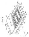
- FIG. 2 is a perspective view of a display panel in a picture display unit according to the present embodiment, in which one part of the panel is cut in order to show an inner structure.
- reference numeral 915 denotes a rear plate, reference numeral 916 a side wall, and reference numeral 917 a face plate.
- the rear plate 915, the side wall 916 and the face plate 917 forms an airtight vessel for keeping the inside of the display panel into a vacuum.
- the sealing is achieved, for example, by applying frit glass to the joining areas and baking it at 400 to 500°C for 10 minutes or longer in atmospheric air or a nitrogenous atmosphere. A method for evacuating the inside of an airtight vessel to a vacuum will be described later.
- a spacer 920 is provided so as to make the airtight vessel an ambient-pressure resistant structure.
- a substrate having an antistatic film is used, which is produced by using the above described mixture targets having various composition concentration ratios in forming films.
- a substrate 911 is fixed on a rear plate 915, while having N ⁇ M pieces of surface conduction electron-emitting devices 912 formed thereon.
- the above described N ⁇ M pieces of surface conduction electron-emitting devices are simple-matrix-wired by M lines of row-directional wiring 913 and N lines of column-directional wiring 914.
- the part composed by the substrate 911, the surface conduction electron-emitting devices 912, the row-directional wiring 913 and the column-directional wiring 914 is called an electron source substrate.
- a fluorescent screen 918 is formed on the undersurface of a faceplate 917.
- a metal back 919 which is well known in the field of CRT, is arranged on the surface of the rear plate side of the fluorescent screen 918.
- Dx1 to Dxm, Dy1 to Dyn and Hv are terminals for electric connection having an airtight structure, which is arranged for electrically connecting the display panel to a not-shown electric circuit.
- Terminals D ⁇ 1 to Dxm are electrically connected to the row-directional wiring 913 of the surface conduction electron-emitting devices, terminals Dy1 to Dyn to the column-directional wiring 914 of the surface conduction electron-emitting devices, and Hv to a metal back (a metallic membrane) of a face plate 919.
- the airtight vessel In order to evacuate the inside of an airtight vessel to a vacuum, the airtight vessel is assembled, a not-shown exhaust pipe is connected with a vacuum pump, and the inside of the airtight vessel is evacuated to a vacuum of 10 -5 [Pa] or lower. Afterwards, the exhaust pipe is sealed. Then, in order to keep the vacuum in the airtight vessel, a getter film (not shown) is formed just before or after sealing, on a predetermined position in the airtight vessel.
- the getter film is formed by heating and evaporating a getter material containing, for instance, Ba as a main component with a heater or high-frequency heating, and by the adsorption effect of the getter film, the inside of the airtight vessel is kept to a vacuum of 1 ⁇ 10 -3 to 1 ⁇ 10 -5 [Pa].
- each surface conduction electron-emitting device 912 when electric voltage is applied to each surface conduction electron-emitting device 912 through terminals outside a vessel, Dx1 to Dxm and Dy1 to Dyn, electrons are emitted from each surface conduction electron-emitting device 912. Concurrently with it, a high pressure of several hundreds [V] to several thousands [V] is applied to a metal back (metal membrane) 919 through the terminals outside the vessel Hv to accelerate the above described emitted electrons and make them collide with the inner surface of a face plate 917. Thereby, each phosphor of each color composing a phosphor layer 918 is activated to emit light, and images are displayed.
- voltage applied to the surface conduction electron-emitting device 912 according to the present invention is around 12 to 16 [V]
- a distance d between a metal back (a metal membrane) 919 and the surface conduction electron-emitting device 912 is around 0.1 to 8 [mm]
- voltage between the metal back (the metal membrane) 919 and the surface conduction electron-emitting device 912 is about 0.1 [kV] to 12 [kV].
- the spacer can be used not only for the picture display unit, but also as a light-emitting source substituted for a light-emitting diode of an optical printer constituted by a photosensitive drum and a light-emitting diode.
- the spacer can be applied to not only a line-shaped light-emitting source but also a two-dimensional light-emitting source.
- a usable body to be irradiated with electron can be not only a material directly emitting light such as a phosphor, but also a member on which a latent image is formed by the electrostatic charge of electrons.
- the present invention can be applied to an electron-generating device, even when a material other than an image-forming member such as a phosphor is used as a body to be irradiated with the electrons emitted from an electron source, like in an electron microscope.
- a spacer substrate was prepared by forming a resistive film according to the present invention as an antistatic film on a glass substrate, and was used as a spacer in a picture display unit using the surface conduction electron-emitting device, which is the present embodiment.
- the evaluation was carried out by placing a display device in an adequately bright room, and making the 50 subjects of adult men and women visually observe a display image at a place 1m apart from the panel face.
- the performance of a resistive film according to the present invention was evaluated by installing a spacer provided with the resistive film in a display device, and measuring the deviation of an electron beam ⁇ L in an image affected by the spacer.
- atomic% indicates the proportion of the number of atoms of monoatoms
- a Pt/Al weight ratio is calculated by (atomic% of Pt ⁇ atomic weight of Pt)/(atomic% of Al ⁇ atomic weight of Al).
- the raw materials of Pt and Al were weighed out so as to have the composition ratio of 5 atomic% Pt to 95 atomic% Al, and then were mixed.
- the mixed materials were melted in a vacuum melting furnace to produce an alloy.
- the alloy was cooled, and then was forge-rolled to further uniformize the component distribution.
- the melted alloy was pressure-baked in a vacuum, and was molded so as to acquire a predetermined plate thickness and shape suitable for a sputtering target, and the product became a Pt-Al-melted alloy mixture target.
- the density of the Pt-Al-melted alloy was 3.6 g/cm 3 .
- a Pt-Al-melted alloy was installed as the target of a high-frequency sputtering apparatus shown in FIG. 3, the flow rate of N 2 was set to 100 sccm, and a Pt-Al mixture-nitrided film was formed with varied total pressures.
- the obtained Pt-Al mixture-nitrided film had the resistivity shown in FIG. 4.
- Pt-Al mixture-nitrided film was analyzed with the use of an RBS (Rutherford backscattering Spectrometory) method, and had the composition shown in Table 2.
- the density of the Pt-Al mixture-nitrided film was 3.5 g/cm 3 .
- Example 2 Similarly to the Example 1, a Pt-Al mixture-nitrided film was formed, and had resistivity shown in FIG. 4.
- Pt-Al mixture-nitrided film was analyzed with the use of an RBS (Rutherford backscattering Spectrometory) method, and had a composition shown in Table 1.
- the density of the Pt-Al mixture-nitrided film was 3.0 g/cm 3 .
- the powders of Pt and AlN were weighed out so as to have the composition ratio of 5 atomic% Pt to 95 atomic% AlN, and then were mixed.
- the powders were mixed with a ball mill in a non-oxidization atmosphere of nitrogen gas. After having been mixed, the powders were classified with a sieve to acquire a further uniformized granular form. Thus mixed powder was calcined in a vacuum.
- the mixed powder obtained through pulverization was pressure-baked in a vacuum to provide a sintered compact.
- a hot pressing process of heating the mixed powder to 1,500°C at the pressure of 2 MPa was employed.
- the sintered compact was formed so as to acquire a predetermined plate thickness and shape suitable for a sputtering target, and thus a Pt-AlN mixture sintered target was obtained.
- the Pt-AlN sintered compact had the density of 2.4 g/cm 3 .
- the N 2 flow rate was set to 100 sccm, and a Pt-AlN mixture-nitrided film was formed with varied total pressures. Then, the obtained film had resistivity shown in FIG. 5.
- Pt-AlN mixture-nitrided film was analyzed with the use of an RBS (Rutherford backscattering Spectrometory) method, and was proved to have the composition shown in Table 3.
- the Pt-AlN mixture-nitrided film had the density of 3.2 g/cm 3 .
- Example 3 instead of metallic aluminum, aluminum nitride was used as a raw material, and the raw materials were weighed out so as to have the composition ratio of 3 atomic% Pt to 97 atomic% AlN, then, were mixed, calcinated, pulverized, and pressure-baked. Thus, a Pt-AlN mixture sintered target was obtained.
- the Pt-AlN sintered compact had the density of 2.0 g/cm 3 .
- Example 2 Similarly to the Example 1, a N 2 flow rate was set to 100 sccm, and a Pt-AlN mixture-nitrided film was formed with varied total pressures. Then, the obtained film had resistivity shown in FIG. 5.
- Pt-AlN mixture-nitrided film was analyzed with the use of an RBS (Rutherford backscattering) method, and was proved to have the composition shown in Table 3.
- the Pt-AlN mixture-nitrided film had the density of 2.8 g/cm 3 .
- a glass substrate was introduced into a film-forming chamber, and a film was formed on it. Sputtering time was 30 minutes.
- resistive film had the film thickness of 200 nm, and the resistivity of 2 ⁇ 10 9 ⁇ cm.
- Pt-Al mixture-nitrided film was subjected to the measurement of the average particle diameter of platinum particles dispersed in the medium of aluminum nitride through a TEM (transmission electron microscope), and showed the diameter of 0.4 nm.
- a glass substrate was introduced into a film-forming chamber, and the film was formed on it. After the sputtering time of 25 minutes, a resistive film having the thickness of 200 nm was obtained. The obtained resistive film had the resistivity of 1 ⁇ 10 9 ⁇ cm.
- Pt-Al mixture-nitrided film was subjected to the measurement of the average particle diameter of platinum particles dispersed in the medium of aluminum nitride through a TEM (transmission electron microscope), and showed the average particle diameter of 0.5 nm.
- a glass substrate was introduced into a film-forming chamber, and the film was formed on it. After the sputtering time of 20 minutes, a resistive film having the thickness of 200 nm was obtained. The obtained resistive film had the resistivity of 8 ⁇ 10 8 ⁇ cm.
- Pt-Al mixture-nitrided film was subjected to the measurement of the average particle diameter of platinum particles dispersed in the medium of aluminum nitride through a TEM (transmission electron microscope), and showed the average particle diameter of 0.6 nm.
- a glass substrate was introduced into a film-forming chamber, and the film was formed on it. After the sputtering time of 30 minutes, a resistive film having the thickness of 200 nm was obtained. The obtained resistive film had the resistivity of 1 ⁇ 10 4 ⁇ cm.
- Pt-Al mixture-nitrided film was subjected to the measurement of the average particle diameter of platinum particles dispersed in the medium of aluminum nitride through a TEM (transmission electron microscope), and showed the average particle diameter of 9 nm.
- a glass substrate was introduced into a film-forming chamber, and the film was formed on it. After the sputtering time of 25 minutes, a resistive film having the thickness of 200 nm was obtained. The obtained resistive film had the resistivity of 1 ⁇ 10 4 ⁇ cm.
- Pt-Al mixture-nitrided film was subjected to the measurement of the average particle diameter of platinum particles dispersed in the medium of aluminum nitride through a TEM (transmission electron microscope), and showed the average particle diameter of 10 nm.
- a glass substrate was introduced into a film-forming chamber, and the film was formed on it. After the sputtering time of 20 minutes, a resistive film having the thickness of 200 nm was obtained. The obtained resistive film had the resistivity of 1x10 0 ⁇ cm.
- Pt-Al mixture-nitrided film was subjected to the measurement of the average particle diameter of platinum particles dispersed in the medium of aluminum nitride through a TEM (transmission electron microscope), and showed the average particle diameter of 11 nm.
- a sputtering pressure was set to 1.0 Pa, and an electrification power to 2,400 W.
- the resistive film had the resistivity of 1 ⁇ 10 11 ⁇ cm.
- Pt-Al mixture-nitrided film was subjected to the measurement of the average particle diameter of platinum particles dispersed in the medium of aluminum nitride through a TEM (transmission electron microscope), and showed the average particle diameter of 0.8 nm.
- a sputtering pressure was set to 0.5 Pa, and an electrification power to 2,400 W.
- the resistive film had the resistivity of 1 ⁇ 10 11 ⁇ cm.
- Pt-Al mixture-nitrided film was subjected to the measurement of the average particle diameter of platinum particles dispersed in the medium of aluminum nitride through a TEM (transmission electron microscope), and showed the average particle diameter of 1 nm.
- a sputtering pressure was set to 0.3 Pa, and an electrification power to 2,400 W.
- the resistive film had the resistivity of 8 ⁇ 10 10 ⁇ cm.
- Pt-Al mixture-nitrided film was subjected to the measurement of the average particle diameter of platinum particles dispersed in the medium of aluminum nitride through a TEM (transmission electron microscope), and showed the diameter of 2 nm.
- a sputtering pressure was set to 1.0 Pa, and an electrification power to 2,400 W.
- the resistive film had the resistivity of 1 ⁇ 10 4 ⁇ cm.
- Pt-Al mixture-nitrided film was subjected to the measurement of the average particle diameter of platinum particles dispersed in the medium of aluminum nitride through a TEM (transmission electron microscope), and showed the average particle diameter of 9 nm.
- a sputtering pressure was set to 0.5 Pa, and an electrification power to 2,400 W.
- the resistive film had the resistivity of 1 ⁇ 10 4 ⁇ cm.
- Pt-Al mixture-nitrided film was subjected to the measurement of the average particle diameter of platinum particles dispersed in the medium of aluminum nitride through a TEM (transmission electron microscope), and showed the average particle diameter of 10 nm.
- a sputtering pressure was set to 0.3 Pa, and an electrification power to 2,400 W.
- the resistive film had the resistivity of 1 ⁇ 10 2 ⁇ cm.
- Pt-Al mixture-nitrided film was subjected to the measurement of the average particle diameter of platinum particles dispersed in the medium of aluminum nitride through a TEM (transmission electron microscope), and showed the average particle diameter of 11 nm.
- a glass substrate was introduced into a film-forming chamber, and the film was formed on it. After the sputtering time of 70 minutes, a resistive film having the thickness of 200 nm was obtained. The obtained resistive film had the resistivity of 5 ⁇ 10 11 ⁇ cm.
- Pt-Al mixture-oxidized film was subjected to the measurement of the average particle diameter of platinum particles dispersed in the medium of aluminum oxide through a TEM (transmission electron microscope), and showed the average particle diameter of 0.4 nm.
- a glass substrate was introduced into a film-forming chamber, and the film was formed on it. After the sputtering time of 65 minutes, a resistive film having the film thickness of 200 nm was obtained. The obtained resistive film had the resistivity of 1 ⁇ 10 11 ⁇ cm.
- Pt-Al mixture-oxidized film was subjected to the measurement of the average particle diameter of platinum particles dispersed in the medium of aluminum oxide through a TEM (transmission electron microscope), and showed the average particle diameter of 0.5 nm.
- a glass substrate was introduced into a film-forming chamber, and the film was formed on it. After the sputtering time of 60 minutes, a resistive film having the film thickness of 200 nm was obtained. The obtained resistive film had the resistivity of 1 ⁇ 10 11 ⁇ cm.
- Pt-Al mixture-oxidized film was subjected to the measurement of the average particle diameter of platinum particles dispersed in the medium of aluminum oxide through a TEM (transmission electron microscope), and showed the average particle diameter of 0.6 nm.
- a glass substrate was introduced into a film-forming chamber, and the film was formed on it. After the sputtering time of 70 minutes, a resistive film having the thickness of 200 nm was obtained. The obtained resistive film had the resistivity of 1 ⁇ 10 8 ⁇ cm.
- Pt-Al mixture-oxidized film was subjected to the measurement of the average particle diameter of platinum particles dispersed in the medium of aluminum oxide through a TEM (transmission electron microscope), and showed the diameter of 8 nm.
- a glass substrate was introduced into a film-forming chamber, and the film was formed on it. After the sputtering time of 65 minutes, a resistive film having the film thickness of 200 nm was obtained. The obtained resistive film had the resistivity of 1 ⁇ 10 7 ⁇ cm.
- Pt-Al mixture-oxidized film was subjected to the measurement of the average particle diameter of platinum particles dispersed in the medium of aluminum oxide through a TEM (transmission electron microscope), and showed the average particle diameter of 9 nm.
- a glass substrate was introduced into a film-forming chamber, and the film was formed on it. After the sputtering time of 60 minutes, a resistive film having the film thickness of 200 nm was obtained. The obtained resistive film had the resistivity of 1 ⁇ 10 6 ⁇ cm.
- Pt-Al mixture-oxidized film was subjected to the measurement of the average particle diameter of platinum particles dispersed in the medium of aluminum oxide through a TEM (transmission electron microscope), and showed the average particle diameter of 10 nm.
- a film was formed with the use of a Pt-Al mixture target having the composition ratio of 2 atomic% Pt to 98 atomic% Al, and the diameter of 8 inches.
- a sputtering pressure was set to 1.0 Pa, and an electrification power to 2,400 W.
- a resistive film having the film thickness of 200 nm was obtained.
- the obtained resistive film had the resistivity of 2 ⁇ 10 12 ⁇ cm.
- Pt-Al mixture-nitrided/oxidized film was subjected to the measurement of the average particle diameter of platinum particles dispersed in the medium of aluminum nitride and aluminum oxide through a TEM (transmission electron microscope), and showed the average particle diameter of 0.4 nm.
- a film was formed with the use of a Pt-Al mixture target having the composition ratio of 2 atomic% Pt to 98 atomic% Al, and the diameter of 8 inches.
- a sputtering pressure was set to 0.5 Pa, and an electrification power to 2,400 W.
- a resistive film having the thickness of 200 nm was obtained.
- the obtained resistive film had the resistivity of 1 ⁇ 10 11 ⁇ cm.
- Pt-Al mixture-nitrided/oxidized film was subjected to the measurement of the average particle diameter of platinum particles dispersed in the medium of aluminum nitride and aluminum oxide through a TEM (transmission electron microscope), and showed the average particle diameter of 0.5 nm.
- a film was formed with the use of a Pt-Al mixture target having the composition ratio of 2 atomic% Pt to 98 atomic% Al, and the diameter of 8 inches.
- a sputtering pressure was set to 0.3 Pa, and an electrification power to 2,400 W.
- the sputtering time was 25 minutes. Then, a resistive film having the film thickness of 200 nm was obtained. The obtained resistive film had the resistivity of 1 ⁇ 10 11 ⁇ cm.
- Pt-Al mixture-nitrided/oxidized film was subjected to the measurement of the average particle diameter of platinum particles dispersed in the medium of aluminum nitride and aluminum oxide through a TEM (transmission electron microscope), and showed the average particle diameter of 0.6 nm.
- a film was formed with the use of a Pt-Al mixture target having the composition ratio of 30 atomic% Pt to 70 atomic% Al, and the diameter of 8 inches.
- a sputtering pressure was set to 1.0 Pa, and an electrification power to 2,400 W.
- a resistive film having the film thickness of 200 nm was obtained.
- the obtained resistive film had the resistivity of 1 ⁇ 10 5 ⁇ cm.
- Pt-Al mixture-nitrided/oxidized film was subjected to the measurement of the average particle diameter of platinum particles dispersed in the medium of aluminum nitride and aluminum oxide through a TEM (transmission electron microscope), and showed the average particle diameter of 9 nm.
- a film was formed with the use of a Pt-Al mixture target having the composition ratio of 30 atomic% Pt to 70 atomic% Al, and the diameter of 8 inches.
- a sputtering pressure was set to 0.5 Pa, and an electrification power to 2,400 W.
- a resistive film having the thickness of 200 nm was obtained.
- the obtained resistive film had the resistivity of 1 ⁇ 10 4 ⁇ cm.
- Pt-Al mixture-nitrided/oxidized film was subjected to the measurement of the average particle diameter of platinum particles dispersed in the medium of aluminum nitride and aluminum oxide through a TEM (transmission electron microscope), and showed the average particle diameter of 10 nm.
- a film was formed with the use of a Pt-Al mixture target having the composition ratio of 30 atomic% Pt to 70 atomic% Al, and the diameter of 8 inches.
- a sputtering pressure was set to 0.3 Pa, and an electrification power to 2,400 W.
- a resistive film having the thickness of 200 nm was obtained.
- the obtained resistive film had the resistivity of 5 ⁇ 10 3 ⁇ cm.
- Pt-Al mixture-nitrided/oxidized film was subjected to the measurement of the average particle diameter of platinum particles dispersed in the medium of aluminum nitride and aluminum oxide through a TEM (transmission electron microscope), and showed the average particle diameter of 11 nm.
- a spacer substrate was prepared by forming each resistive film shown in the above described samples 5 to 28 as an antistatic film on a glass substrate, and was used as a spacer in a picture display unit using the surface conduction electron-emitting device, which is the present embodiment.
- the influence of the spacer on an image was evaluated by measuring the deviation of an electron beam ⁇ L.
- a film was formed with the use of a Pt-Ge mixture target prepared so as to have an adjusted composition ratio and the diameter of 8 inches.
- the following 4 kinds of gas types were used in order to form the film: a nitrogen/Ar mixed gas, nitrogen gas, oxygen gas and an oxygen/nitrogen mixed gas.
- a sputtering pressure was set to 0.3 Pa to 1.5 Pa, and an electrification power to 2,400 W.
- a sputtering time of period was appropriately adjusted so that film thickness can be 200 nm.
- a spacer substrate was prepared by forming each resistive film on a glass substrate, and was used as a spacer in a picture display unit using a surface conduction electron-emitting device, which is the present embodiment.
- the influence of the spacer on an image was evaluated by measuring the deviation of an electron beam ⁇ L.
- a film was formed with the use of a Pt-Si mixture target prepared so as to have an adjusted composition ratio and the diameter of 8 inches.
- the following 4 kinds of gas types were used in order to form the film: a nitrogen/Ar mixed gas, nitrogen gas, oxygen gas and an oxygen/nitrogen mixed gas.
- a sputtering pressure was set to 0.3 to 1.5 Pa, and an electrification power to 2,400 W.
- a sputtering time of period was appropriately adjusted so that film thickness can be 200 nm.
- a spacer substrate was prepared by forming each resistive film on a glass substrate, and was used as a spacer in a picture display unit using the surface conduction electron-emitting device, which is the present embodiment.
- the influence of the spacer on an image was evaluated by measuring the deviation of an electron beam ⁇ L.
- a film was formed with the use of a Pt-Mg mixture target prepared so as to have an adjusted composition ratio and the diameter of 8 inches.
- the following 4 kinds of gas types were used in order to form the film: a nitrogen/Ar mixed gas, nitrogen gas, oxygen gas and an oxygen/nitrogen mixed gas.
- a sputtering pressure was set to 0.3 to 1.5 Pa, and an electrification power to 2,400 W.
- a sputtering time of period was appropriately adjusted so that film thickness can be 200 nm.
- a spacer substrate was prepared by forming each resistive film on a glass substrate, and was used as a spacer in a picture display unit using the surface conduction electron-emitting device, which is the present embodiment.
- the influence of the spacer on an image was evaluated by measuring the deviation of an electron beam ⁇ L.
- a film was formed with the use of an Au-Al mixture target having a composition ratio adjusted so as to comprise gold for a particle material, and aluminum nitride, aluminum oxide or aluminum nitride/oxide for a medium, and having the diameter of 8 inches.
- the following 4 kinds of gas types were used in order to form the film: a nitrogen/Ar mixed gas, nitrogen gas, oxygen gas and an oxygen/nitrogen mixed gas.
- a sputtering pressure was set to 0.3 to 1.5 Pa, and an electrification power to 2,400 W.
- a sputtering time of period was appropriately adjusted so that film thickness can be 200 nm.
- a spacer substrate was prepared by forming each resistive film on a glass substrate, and was used as a spacer in a picture display unit using the surface conduction electron-emitting device, which is the present embodiment.
- the influence of the spacer on an image was evaluated by measuring the deviation of an electron beam ⁇ L.
- a film was formed with the use of an Au-Ge mixture target having a composition ratio adjusted so as to comprise gold for a particle material, and germanium nitride, germanium oxide or germanium nitride/oxide for a medium, and having the diameter of 8 inches.
- the following 4 kinds of gas types were used in order to form the film: a nitrogen/Ar mixed gas, nitrogen gas, oxygen gas and an oxygen/nitrogen mixed gas.
- a sputtering pressure was set to 0.3 to 1.5 Pa, and an electrification power to 2,400 W.
- a sputtering time of period was appropriately adjusted so that film thickness can be 200 nm.
- a spacer substrate was prepared by forming each resistive film on a glass substrate, and was used as a spacer in a picture display unit using the surface conduction electron-emitting device, which is the present embodiment.
- the influence of the spacer on an image was evaluated by measuring the deviation of an electron beam ⁇ L.
- a film was formed with the use of an Au-Si mixture target having a composition ratio adjusted so as to comprise gold for a particle material, and silicon nitride, silicon oxide or silicon nitride/oxide for a medium, and having the diameter of 8 inches.
- the following 4 kinds of gas types were used in order to form the film: a nitrogen/Ar mixed gas, nitrogen gas, oxygen gas and an oxygen/nitrogen mixed gas.
- a sputtering pressure was set to 0.3 to 1.5 Pa, and an electrification power to 2,400 W.
- a sputtering time of period was appropriately adjusted so that film thickness can be 200 nm.
- a spacer substrate was prepared by forming each resistive film on a glass substrate, and was used as a spacer in a picture display unit using the surface conduction electron-emitting device, which is the present embodiment.
- the influence of the spacer on an image was evaluated by measuring the deviation of an electron beam ⁇ L.
- a film was formed with the use of an Au-Mg mixture target having a composition ratio adjusted so as to comprise gold for a particle material, and magnesium nitride, magnesium oxide or magnesium nitride/oxide for a medium, and having the diameter of 8 inches.
- the following 4 kinds of gas types were used in order to form the film: a nitrogen/Ar mixed gas, nitrogen gas, oxygen gas and an oxygen/nitrogen mixed gas.
- a sputtering pressure was set to 0.3 to 1.5 Pa, and an electrification power to 2,400 W.
- a sputtering time of period was appropriately adjusted so that film thickness can be 200 nm.
- a spacer substrate was prepared by forming each resistive film on a glass substrate, and was used as a spacer in a picture display unit using the surface conduction electron-emitting device, which is the present embodiment.
- the influence of the spacer on an image was evaluated by measuring the deviation of an electron beam ⁇ L.
- a film was formed with the use of an Ag-Al mixture target having a composition ratio adjusted so as to comprise silver for a particle material, and aluminum nitride, aluminum oxide or aluminum nitride/oxide for a medium, and having the diameter of 8 inches.
- the following 4 kinds of gas types were used in order to form the film: a nitrogen/Ar mixed gas, nitrogen gas, oxygen gas and an oxygen/nitrogen mixed gas.
- a sputtering pressure was set to 0.3 to 1.5 Pa, and an electrification power to 2,400 W.
- a sputtering time of period was appropriately adjusted so that film thickness can be 200 nm.
- a spacer substrate was prepared by forming each resistive film on a glass substrate, and was used as a spacer in a picture display unit using the surface conduction electron-emitting device, which is the present embodiment.
- the influence of the spacer on an image was evaluated by measuring the deviation of an electron beam ⁇ L.
- a film was formed with the use of an Ag-Ge mixture target having a composition ratio adjusted so as to comprise silver for a particle material, and germanium nitride, germanium oxide or germanium nitride/oxide for a medium, and having the diameter of 8 inches.
- the following 4 kinds of gas types were used in order to form the film: a nitrogen/Ar mixed gas, nitrogen gas, oxygen gas and an oxygen/nitrogen mixed gas.
- a sputtering pressure was set to 0.3 to 1.5 Pa, and an electrification power to 2,400 W.
- a sputtering time of period was appropriately adjusted so that film thickness can be 200 nm.
- a spacer substrate was prepared by forming each resistive film on a glass substrate, and was used as a spacer in a picture display unit using the surface conduction electron-emitting device, which is the present embodiment.
- the influence of the spacer on an image was evaluated by measuring the deviation of an electron beam ⁇ L.
- a film was formed with the use of an Ag-Si mixture target having a composition ratio adjusted so as to comprise silver for a particle material, and silicon nitride, silicon oxide or silicon nitride/oxide for a medium, and having the diameter of 8 inches.
- the following 4 kinds of gas types were used in order to form the film: a nitrogen/Ar mixed gas, nitrogen gas, oxygen gas and an oxygen/nitrogen mixed gas.
- a sputtering pressure was set to 0.3 to 1.5 Pa, and an electrification power to 2,400 W.
- a sputtering time of period was appropriately adjusted so that film thickness can be 200 nm.
- a spacer substrate was prepared by forming each resistive film on a glass substrate, and was used as a spacer in a picture display unit using the surface conduction electron-emitting device, which is the present embodiment.
- the influence of the spacer on an image was evaluated by measuring the deviation of an electron beam ⁇ L.
- a film was formed with the use of an Ag-Mg mixture target having a composition ratio adjusted so as to comprise silver for a particle material, and magnesium nitride, magnesium oxide or magnesium nitride/oxide for a medium, and having the diameter of 8 inches.
- the following 4 kinds of gas types were used in order to form the film: a nitrogen/Ar mixed gas, nitrogen gas, oxygen gas and an oxygen/nitrogen mixed gas.
- a sputtering pressure was set to 0.3 to 1.5 Pa, and an electrification power to 2,400 W.
- a sputtering time of period was appropriately adjusted so that film thickness can be 200 nm.
- a spacer substrate was prepared by forming each resistive film on a glass substrate, and was used as a spacer in a picture display unit using the surface conduction electron-emitting device, which is the present embodiment.
- the influence of the spacer on an image was evaluated by measuring the deviation of an electron beam ⁇ L.
- a film was formed with the use of a Ge-Al mixture target having a composition ratio adjusted so as to comprise germanium for a particle material, and aluminum nitride, aluminum oxide or aluminum nitride/oxide for a medium, and having the diameter of 8 inches.
- the following 4 kinds of gas types were used in order to form the film: a nitrogen/Ar mixed gas, nitrogen gas, oxygen gas and an oxygen/nitrogen mixed gas.
- a sputtering pressure was set to 0.3 to 1.5 Pa, and an electrification power to 2,400 W.
- a sputtering time of period was appropriately adjusted so that film thickness can be 200 nm.
- a spacer substrate was prepared by forming each resistive film on a glass substrate, and was used as a spacer in a picture display unit using the surface conduction electron-emitting device, which is the present embodiment.
- the influence of the spacer on an image was evaluated by measuring the deviation of an electron beam ⁇ L.
- a film was formed with the use of a Ge-Si mixture target having a composition ratio adjusted so as to comprise germanium for a particle material, and silicon nitride, silicon oxide or silicon nitride/oxide for a medium, and having the diameter of 8 inches.
- the following 4 kinds of gas types were used in order to form the film: a nitrogen/Ar mixed gas, nitrogen gas, oxygen gas and an oxygen/nitrogen mixed gas.
- a sputtering pressure was set to 0.3 to 1.5 Pa, and an electrification power to 2,400 W.
- a sputtering time of period was appropriately adjusted so that film thickness can be 200 nm.
- a spacer substrate was prepared by forming each resistive film on a glass substrate, and was used as a spacer in a picture display unit using the surface conduction electron-emitting device, which is the present embodiment.
- the influence of the spacer on an image was evaluated by measuring the deviation of an electron beam ⁇ L.
- a film was formed with the use of a Ge-Mg mixture target having a composition ratio adjusted so as to comprise germanium for a particle material, and magnesium nitride, magnesium oxide or magnesium nitride/oxide for a medium, and having the diameter of 8 inches.
- the following 4 kinds of gas types were used in order to form the film: a nitrogen/Ar mixed gas, nitrogen gas, oxygen gas and an oxygen/nitrogen mixed gas.
- a sputtering pressure was set to 0.3 to 1.5 Pa, and an electrification power to 2,400 W.
- a sputtering time of period was appropriately adjusted so that film thickness can be 200 nm.
- a spacer substrate was prepared by forming each resistive film on a glass substrate, and was used as a spacer in a picture display unit using the surface conduction electron-emitting device, which is the present embodiment.
- the influence of the spacer on an image was evaluated by measuring the deviation of an electron beam ⁇ L.
- a film was formed with the use of a Si-Al mixture target having a composition ratio adjusted so as to comprise silicon for a particle material, and aluminum nitride, aluminum oxide or aluminum nitride/oxide for a medium, and having the diameter of 8 inches.
- the following 4 kinds of gas types were used in order to form the film: a nitrogen/Ar mixed gas, nitrogen gas, oxygen gas and an oxygen/nitrogen mixed gas.
- a sputtering pressure was set to 0.3 to 1.5 Pa, and an electrification power to 2,400 W.
- a sputtering time of period was appropriately adjusted so that film thickness can be 200 nm.
- a spacer substrate was prepared by forming each resistive film on a glass substrate, and was used as a spacer in a picture display unit using the surface conduction electron-emitting device, which is the present embodiment.
- the influence of the spacer on an image was evaluated by measuring the deviation of an electron beam ⁇ L.
- a film was formed with the use of an Si-Ge mixture target having a composition ratio adjusted so as to comprise silicon for a particle material, and germanium nitride, germanium oxide or germanium nitride/oxide for a medium, and having the diameter of 8 inches.
- the following 4 kinds of gas types were used in order to form the film: a nitrogen/Ar mixed gas, nitrogen gas, oxygen gas and an oxygen/nitrogen mixed gas.
- a sputtering pressure was set to 0.3 to 1.5 Pa, and an electrification power to 2,400 W.
- a sputtering time of period was appropriately adjusted so that film thickness can be 200 nm.
- a spacer substrate was prepared by forming each resistive film on a glass substrate, and was used as a spacer in a picture display unit using the surface conduction electron-emitting device, which is the present embodiment.
- the influence of the spacer on an image was evaluated by measuring the deviation of an electron beam ⁇ L.
- a film was formed with the use of a Si-Mg mixture target having a composition ratio adjusted so as to comprise silicon for a particle material, and magnesium nitride, magnesium oxide or magnesium nitride/oxide for a medium, and having the diameter of 8 inches.
- the following 4 kinds of gas types were used in order to form the film: a nitrogen/Ar mixed gas, nitrogen gas, oxygen gas and an oxygen/nitrogen mixed gas.
- a sputtering pressure was set to 0.3 to 1.5 Pa, and an electrification power to 2,400 W.
- a sputtering time of period was appropriately adjusted so that film thickness can be 200 nm.
- a spacer substrate was prepared by forming each resistive film on a glass substrate, and was used as a spacer in a picture display unit using the surface conduction electron-emitting device, which is the present embodiment.
- the influence of the spacer on an image was evaluated by measuring the deviation of an electron beam ⁇ L.
- the present invention can provide the resistive film which is superior controllability for a resistivity value, stability and reproducibility, has adequate temperature characteristics of resistance, and is suitable for an antistatic film.
- the present invention can provide a picture display unit having the effect of reducing the instability of a display image, which originates from a temperature distribution in an airtight vessel caused by a temperature difference between a pair of substrates that compose the airtight vessel, and having superior display performance.
- An antistatic film installed in an airtight vessel containing an electron source of an electron-generating device such as a picture display unit has a structure comprising an image of conductor particles with particle diameters of 0.5 to 10 nm dispersed in a medium containing a nitride; and thereby improves controllability for a resistivity value, stability and reproducibility, and the adequate temperature characteristics of resistance.
Abstract
Description
- The present invention relates to an antistatic film installed in an airtight vessel containing an electron source of an electron-generating device such as a picture display unit, to a spacer using it, and to the picture display unit.
- A flat display unit using an electron-emitting device has, as shown in Japanese Patent Application Laid-Open No. H10-284286, a spacer called as the spacer or a rib installed therein, which is a structural support resistant to ambient pressure for keeping the inside of the unit into a high vacuum.
- FIG. 7 is a cross-sectional schematic view of an image-forming apparatus using many electron-emitting devices.
Reference numeral 101 denotes a rear plate, reference numeral 102 a sidewall and reference numeral 103 a faceplate, and an airtight vessel is formed by therear plate 101, theside wall 102 and theface plate 103. Aspacer 107b that is a structural support resistant to ambient pressure in the airtight vessel has a low-resistivity film 110 thereon, and is connected to wiring 109 through anelectroconductive frit 108. - An electron-
emitting device 104 is formed on arear plate 101, and aphosphor 105 and ametal back 106 are formed on a face plate. Objects of providing ametal back 106 are to improve a utilization factor of light by mirror-reflecting a light emitted from aphosphor 105; to protect thephosphor 105 from the collision of negative ions; to work as an electrode for applying an electron beam-accelerating voltage; and to work as a conducting path for electrons after having excited thephosphor 105. - A
spacer 107a shows the electrostatically charged state of the spacer, and shows a state in which electrostatic charge (positive electrostatic charge in the drawing) is caused by collision of one part of electrons emitted from an electron source around it. Here, thespacer 107a shows the electrostatically charged state of the spacer when having noantistatic film 112 installed thereon, and thus, the thickness of a low-resistivity film is drawn more thickly than the low-resistivity film 110 contacting with theantistatic film 112 of thespacer 107b, for convenience in illustration. - When a
spacer 107a is positively charged with electricity as described above, electrons emitted from an electron-emitting device 104 that is an electron source are drawn to a spacer side, for example, like anelectron trajectory 111a, and consequently impair the quality of a displayed image. - In order to solve the problem, there is a proposition of arranging an
antistatic film 112 on aspacer 107b, eliminating the charge by passing a micro electrical current through the surface, and thereby making electrons draw a predetermined trajectory such as anelectron trajectory 111b, without being drawn to the spacer. There is also a proposition, as shown in Japanese Patent Application Laid-Open No. 2001-143620, of providing unevenness on the surface of a spacer glass substrate to make an effective secondary emission coefficient less than that with a flat spacer surface, and to effectively inhibit the electrostatic charge of the spacer surface. - Furthermore, Japanese Patent Application Laid-Open No. H10-284283 proposes a spacer coated with an electrostatic charge-mitigating film containing aluminum nitride or aluminum oxide, and noble metals such as gold, palladium and platinum, by binary simultaneous sputtering with the use of an aluminum target and a noble metal target, and of a mixed gas of argon and nitrogen or oxygen as a gas for forming a film.
- However, it has become clear that the spacers shown in the above described conventional examples cause variation in the performance of the function for eliminating electrostatic charge.
- In particular, when a temperature distribution is formed in the spacer, the distribution of resistivity is also formed due to the temperature characteristic of the resistivity of the antistatic film. The variation of resistivity leads to the variation in the diselectrification function.
- Specifically, in a flat display panel, the instability of a display image results from temperature distribution in a panel plane, which is caused by a temperature difference between a face plate and a rear plate.
- In addition, a conventional method of forming an antistatic film containing a plurality of elements by sputtering simultaneously a plurality of different material targets (for example, binary sputtering with the use of two materials) might cause variation in the resistivity of an antistatic film depending on each film-forming batch even when film-forming conditions (background, sputtering pressure, gas flow rate and target electrification power) are uniformized.
- In order to uniformize resistivity, target electrification powers supplied to different material targets are required to be adjusted to each, which is complicated, and the operation is not always highly reproducible. In particular, in binary sputtering, when there is a large difference between target electrification powers, so-called cross contamination can not be avoided, which is a phenomenon that a more powerfully electrified target material deposits on the surface of a less powerfully electrified target material.
- An object of the present invention is to provide an antistatic film having superior controllability for a resistivity value, stability and reproducibility, and the adequate temperature characteristics of resistance.
- The present invention provides an antistatic film having a structure comprising a plurality of conductor particles with particle diameters of 0.5 to 10 nm dispersed in a medium containing a nitride.
- In addition, the present invention provides an antistatic film having a structure comprising a plurality of conductor particles with particle diameters of 0.5 to 10 nm dispersed in a medium containing an oxide.
- In addition, the present invention provides an antistatic film having a structure comprising a plurality of conductor particles with particle diameters of 0.5 to 10 nm dispersed in a medium containing a nitride and an oxide.
- In addition, the present invention provides an antistatic film having a structure comprising a plurality of semiconductor particles with particle diameters of 0.5 to 10 nm dispersed in a medium containing a nitride.
- In addition, the present invention provides an antistatic film having a structure comprising a plurality of semiconductor particles with particle diameters of 0.5 to 10 nm dispersed in a medium containing an oxide.
- In addition, the present invention provides an antistatic film having a structure of dispersing a plurality of semiconductive particles with particle diameters of 0.5 to 10 nm in a medium containing a nitride and an oxide.
As for media,which it was described above, it points at the part except for the particles which have the particle diameters of 0.5 to 10nm dispersed in a film and which exists. - In addition, the present invention provides an electron-generating device with an electron source in an airtight vessel, comprising any of the above described antistatic films in the airtight vessel.
- In addition, the present invention provides a picture display unit provided with an airtight vessel having a first substrate with an electron source arranged thereon, and a second substrate with an image display member arranged thereon so as to face the electron source, and a spacer arranged between the first and second substrates in the above described airtight vessel, wherein the spacer has any of the above described antistatic films arranged on the surface.
- In addition, the present invention provides a spacer arranged between a first substrate and a second substrate in a picture display unit provided with an airtight vessel having the first substrate with an electron source arranged thereon and the second substrate having an image display member arranged thereon so as to face the electron source, wherein the spacer has any of the above described antistatic films on the surface.
-
- FIG. 1 is a schematic view showing the cross-sectional shape of an antistatic film according to the present invention, observed with a TEM (a transmission electron microscope);
- FIG. 2 is a perspective view showing a picture display unit according to the present invention, of which one part of the display panel is cut;
- FIG. 3 is a block diagram of a high-frequency sputtering apparatus arranging a target according to the present invention therein, which is used for imparting an antistatic film to a spacer substrate;
- FIG. 4 is a figure showing a relation between the resistivity of a Pt-Al mixture-nitride film according to the present invention and the total pressure of a sputtering gas;
- FIG. 5 is a figure showing a relation between the resistivity of a Pt-AlN mixture-nitride film according to the present invention and the total pressure of a sputtering gas;
- FIG. 6 is a figure showing the variation of the resistivity of a Pt-Al mixture-nitride film according to the present invention;
- FIG. 7 is a cross-sectional schematic view of an image-forming apparatus using an electron-emitting device, for describing the mechanism of an electrostatic charge in a spacer according to the present invention; and
- FIG. 8 is a view explaining the deviation of an electron beam ΔL which appears as the disarray of a display image due to the influence of a spacer according to the present invention.
-
- The present invention provides an antistatic film having a structure comprising a plurality of conductor particles with particle diameters of 0.5 to 10 nm dispersed in a medium containing a nitride.
- In addition, the present invention provides an antistatic film having a structure comprising a plurality of conductor particles with particle diameters of 0.5 to 10 nm dispersed in a medium containing an oxide.
- In addition, the present invention provides an antistatic film having a structure comprising a plurality of conductor particles with particle diameters of 0.5 to 10 nm dispersed in a medium containing a nitride and an oxide.
- In addition, the conductor particle is preferably a noble metal particle.
- In addition, the conductor particle is preferably a platinum particle, and the nitride is preferably aluminum nitride.
- In addition, the conductor particle is preferably a platinum particle, and the oxide is preferably aluminum oxide.
- In addition, the conductor particle is preferably a platinum particle, a nitride is preferably aluminum nitride, and the oxide is preferably aluminum oxide.
- In addition, the conductor particle is preferably a gold particle, and the nitride is preferably aluminum nitride.
- In addition, the conductive particle is preferably a gold particle, and the oxide is preferably aluminum oxide.
- In addition, the conductor particle is preferably a gold particle, the nitride is preferably aluminum nitride, and the oxide is preferably aluminum oxide.
- In addition, the conductor particle is preferably a silver particle, and the nitride is preferably aluminum nitride.
- In addition, the conductor particle is preferably a silver particle, and the oxide is preferably aluminum oxide.
- In addition, the conductor particle is preferably a silver particle, the nitride is preferably aluminum nitride, and the oxide is preferably aluminum oxide.
- In addition, the content of the conductor is preferably 0.1 to 10 atomic%.
- In addition, the present invention provides an antistatic film having a structure comprising a plurality of semiconductor particles with particle diameters of 0.5 to 10 nm dispersed in a medium containing a nitride.
- In addition, the present invention provides an antistatic film having a structure comprising a plurality of semiconductor particles with particle diameters of 0.5 to 10 nm dispersed in a medium containing an oxide.
- In addition, the present invention provides an antistatic film having a structure of dispersing a plurality of semiconductive particles with particle diameters of 0.5 to 10 nm in a medium containing a nitride and an oxide.
- In addition, the semiconductor particle is preferably a germanium particle, and the nitride is preferably silicon nitride.
- In addition, the semiconductor particle is preferably a germanium particle, and the oxide is preferably silicon oxide.
- In addition, the conductor particle is preferably a germanium particle, the nitride is preferably silicon nitride, and the oxide is preferably silicon oxide.
- In addition, the content of the semiconductor is preferably 0.1 to 10 atomic%.
- In addition, any of the above described antistatic films includes the particle with a diameter of 1.0 to 9.0 nm, and has a resistivity of ρ = 1×10⁴ to 1×10¹¹ Ωcm.
- In addition, the present invention provides an electron-generating device with an electron source in an airtight vessel, comprising any of the above described antistatic films in the airtight vessel.
- In addition, the present invention provides a picture display unit provided with an airtight vessel having a first substrate with an electron source arranged thereon, and a second substrate with an image display member arranged thereon so as to face the electron source, and a spacer arranged between the first and second substrates in the above described airtight vessel, wherein the spacer has any of the above described antistatic films arranged on the surface.
- In addition, the present invention provides a spacer arranged between a first substrate and a second substrate in a picture display unit provided with an airtight vessel having the first substrate with an electron source arranged thereon and the second substrate having an image display member arranged thereon so as to face the electron source, wherein the spacer has any of the above described antistatic films on the surface.
- The above described antistatic film according to the present invention has little change of resistivity due to temperature, and when the antistatic film is provided particularly on the surface of the spacer of the picture display unit, it has the effect of reducing the instability of a display image, which originates from a temperature distribution in an airtight vessel caused by a temperature difference between the above described first and second substrates.
- Furthermore, the present invention provides a mixture target of aluminum and platinum including 95 wt.% or more aluminum and platinum, which is used for forming an antistatic film containing aluminum and platinum by a sputtering technique.
- In addition, the present invention provides a mixture target of aluminum nitride and platinum including 95 wt.% or more aluminum and platinum, which is used for forming an antistatic film containing aluminum and platinum by a sputtering technique.
- Furthermore, the present invention provides a method for manufacturing an antistatic film containing aluminum and platinum, comprising sputtering the mixture target in an atmosphere containing only nitrogen.
- In addition, the present invention provides a method for manufacturing an antistatic film containing aluminum and platinum, comprising sputtering the mixture target in an atmosphere containing only oxygen.
- In addition, the present invention provides a method for manufacturing an antistatic film containing aluminum and platinum, comprising sputtering the mixture target in an atmosphere containing nitrogen and oxygen.
- A target according to the present invention, as described above, can be preferably used as a target particularly of a PVD (Physical Vapor Deposition) apparatus such as an electron beam evaporation apparatus and a sputtering apparatus. When the PVD (Physical Vapor Deposition) apparatus employs a target according to the present invention as the target thereof, it can produce a resistive film having high reproducibility, superior controllability of a resistivity value, and temperature characteristics of the resistance.
- In addition, a method for manufacturing an antistatic film according to the present invention has the effect comprising the variation of the resistivity less and the reproducibility of the film characteristic (resistivity) higher than those with binary simultaneous sputtering.
- First of all, an antistatic film according to the present invention is a resistive film as shown in FIG. 1 that is a schematic view showing the cross-sectional shape observed with a TEM (a transmission electron microscope), having a structure comprising a plurality of
particles 1 with an average particle diameter of 0.5 to 10 nm dispersed in amedium 2. Here, the average particle diameter is obtained by measuring the diameters of 20 particles in a cross-sectional shape as shown in FIG. 1 and calculating the average. - If the particles have an average particle diameter of 0.5 nm or larger, preferably 1 nm or larger, a resistive film including them can be judged to have adequate temperature characteristics of resistance. Specifically, the resistive film can be judged to have little variation of resistance due to a temperature change. Accordingly, when the spacer having the resistive film as an antistatic film is used in a picture display unit, the spacer can reduce the disarray of a display image caused by it. In addition, the above described average particle diameter is 10 nm or smaller, and preferably 9 nm or smaller from the viewpoint comprising a resistivity of the resistive film equal to or higher than 1×10⁶ Ωcm.
- As described above, the above described resistive film contains an electron source, is arranged in an airtight vessel having temperature change, and is preferably applied to the resistive film for preventing electrostatic charge in the airtight vessel, namely, to an antistatic film.
- Embodiments according to the present invention will be now described below.
- At first, a first embodiment shows a resistive film having a structure comprising a plurality of conductor particles with particle diameters of 0.5 to 10 nm dispersed in a medium containing a nitride.
- A second embodiment shows a resistive film having a structure comprising a plurality of conductor particles with particle diameters of 0.5 to 10 nm dispersed in a medium containing an oxide.
- A third embodiment shows a resistive film having a structure comprising a plurality of conductor particles with particle diameters of 0.5 to 10 nm dispersed in a medium containing a nitride and an oxide.
- In each embodiment described above, the conductor is preferably a metal such as platinum, gold, silver, and among the metals, particularly preferably is platinum or gold from the viewpoint of stability and controllability for a resistivity value. In addition, the above described nitride is preferably aluminum nitride, germanium nitride, silicon nitride and magnesium nitride, and among them, particularly preferably is aluminum nitride from the viewpoint of stability and controllability for a resistivity value. In addition, the above described oxide is preferably aluminum oxide, germanium oxide, silicon oxide and magnesium oxide, and among them, particularly preferably is aluminum oxide from the viewpoint of stability and controllability for a resistivity value.
In addition, the above described medium containing a nitride and an oxide, particularly preferably is aluminum nitride/oxide from the viewpoint of stability and controllability for a resistivity value, and the adequate temperature characteristics of resistance. - Subsequently, a fourth embodiment shows a resistive film having a structure comprising a plurality of semiconductor particles with particle diameters of 0.5 to 10 nm dispersed in a medium containing a nitride.
- A fifth embodiment shows a resistive film having a structure comprising a plurality of semiconductor particles with particle diameters of 0.5 to 10 nm dispersed in a medium containing an oxide.
- The sixth embodiment shows a resistive film having a structure comprising a plurality of semiconductive particles with particle diameters of 0.5 to 10 nm dispersed in a medium containing a nitride and an oxide.
- In the fourth, fifth and sixth embodiments described above, the above semiconductor is preferably germanium, silicon and the like, and among the semiconductors, is particularly preferably germanium from the viewpoint of stability and controllability for a resistivity value. In addition, the above described nitride is preferably aluminum nitride, germanium nitride, silicon nitride and magnesium nitride, and among them, particularly preferably is silicon nitride from the viewpoint of stability and controllability for a resistivity value. In addition, the above described oxide is preferably aluminum oxide, germanium oxide, silicon oxide and magnesium oxide, and among them, particularly preferably is silicon oxide from the viewpoint of stability and controllability for a resistivity value. In addition, the above described medium containing a nitride and an oxide, particularly preferably is silicon nitride/oxide from the viewpoint of stability and controllability for a resistivity value, and the adequate temperature characteristics of resistance.
- In addition, when the resistive film of each of above described first to sixth embodiments is applied to an antistatic film on the surface of a spacer arranged between first and second substrates particularly of a picture display unit provided with an airtight vessel having the first substrate with an electron source arranged thereon and the second substrate with an image display member arranged so as to face the above described electron source, among electron-generating devices, the above each resistive film has the resistivity preferably of ρ = 1×10⁴ to 1×10¹¹ Ωcm, and has a conductor or semiconductor content preferably of 0.1 to 10 atomic%.
- Subsequently, a method for obtaining the above described resistive film will be described.
- The above described resistive film is preferably formed (1) with a sputtering technique by using a mixture target containing at least a component composing a conductor particle or a semiconductor particle and a component to be nitrided or oxidized for composing a nitride or an oxide, and (2) in a sputtering atmosphere containing nitrogen gas with a nitrogen partial pressure of 70% or higher, or oxygen gas with an oxygen partial pressure of 70% or higher. As a matter of course, the atmosphere may be a mixed gas atmosphere if the partial pressure is in the above described range. In addition, the mixed gas atmosphere is particularly preferably the atmosphere of the gas of nitrogen mixed with oxygen, and in this case, the partial pressure of nitrogen and oxygen is preferably controlled to 70% or more in total.
- The particle diameter can be appropriately varied in the range of 0.5 to 10 nm by changing the component and the ratio in the composition of a mixing target, and a gas sort, a sputtering pressure and an electrification power during film formation by sputtering, in the above described conditions (1) and (2), so that a resistive film can be obtained so as to acquire the resistance controlled to a preferable range for an electron generating device to which the resistive film is applied.
- Subsequently, a sputtering apparatus used for forming the resistive film according to the above described embodiments will be described.
- FIG. 3 shows the configuration of a high-frequency sputtering apparatus used in the present embodiment.
- The summary of the process of forming the above described resistive film by using it will be now described. At first, a
substrate 201 is put on a film-formingtray 202, and is charged into apreliminary exhaust hood 203. The preliminary exhaust hood is exhausted to a vacuum degree of 5×10⁻⁴ [Pa] or lower with avacuum pump 204, and then the film-formingtray 202 is moved to a film-formingchamber 206 by aconveyance roller 205. Then, the film-formingchamber 206 is evacuated to a vacuum of 2×10⁻⁵ [Pa] or less. After the vacuum has been confirmed to have reached the above described value, the specified quantity of a nitrogen gas, an oxygen gas, the mixed gas of argon and nitrogen, the mixed gas of argon and oxygen, or the mixed gas of nitrogen and oxygen is passed into the film-forming chamber through agas introduction pipe 207. An orifice (not shown) is adjusted so that the total pressure of a sputtering gas becomes a predetermined pressure. After an atmosphere (the total pressure of a sputtering gas, a gas flow rate) has become stable, a predetermined power is applied to a high-frequency power source 208. In order to form a resistive film all over the surface of asubstrate 201, a film-formingtray 202 is transported by a transportingroller 205 at the rate of 5 mm/min in the direction of an arrow in the drawing so as to cross directly under.amixture target 209, after sputtering discharge has started. The distance between the substrate and the mixture target is set to 200 mm. - Here, the high voltage of direct current applied to the
mixture target 209 is adjusted by a high-frequency power source 208 so that the variation originating from the transportation of the substrate can be reduced. - The direction of transporting the substrate is not limited to one direction, but one-return transportation or a plurality of return transportation is acceptable. In addition, in some configurations of the apparatus, a film may be formed on the whole surface by rotating the substrate directly under the target.
- Through the above described steps, a resistive film can be formed on a substrate.
- In addition, when a resistive film is to be formed on both sides of a substrate, the film is formed on a surface (a first surface), then a film-forming
tray 202 is returned to apreliminary exhaust hood 203, and thesubstrate 201 is taken out. Subsequently, thesubstrate 201 is reversed, and the above described resistive film is formed on a back surface (a second surface) similarly to the top surface (the first surface). - The resistive film to be formed on each surface of the top surface (a first surface) and the back surface (a second surface) may be a single-layered film with a desired film thickness, or a multilayer film consisting of a plurality of layers, which is produced by using a plurality of targets each having a different composition concentration ratio of the mixture from others.
- Subsequently, a mixture target used in the above described sputtering apparatus will be described.
- Here, a method for producing the above described mixture-sintered target will be described.
- At first, the weight of each powder of the above described components is measured in accordance with various composition concentration ratios, and the powders are mixed. For instance, the powders of Pt and Al, or Pt and AlN are mixed. A mixing device is not limited in particular, but a ball mill may be used. The powders are mixed in a non-oxidative atmosphere of nitrogen gas, Ar gas or the like. After the powders have been mixed, they may be classified by a sieve or the like as needed.
- The mixed powder is calcined in an inert atmosphere of nitrogen gas, Ar gas or the like, or in a vacuum. Alternatively, it may be calcined in a reducing atmosphere of hydrogen or the like. The mixed powder is preferably heated to 800 to 1,500°C, for calcination.
- Thus formed solid material is pulverized. A pulverizing device is not limited in particular, but a ball mill may be used. The solid material is pulverized in a non-oxidative atmosphere of nitrogen gas, Ar gas or the like. After the solid material has been pulverized, the product may be classified with a sieve or the like as needed.
- The mixed powder obtained through pulverization is pressure-baked in an inert atmosphere of nitrogen gas, Ar gas or the like, or in a vacuum, and a sintered compact is thereby obtained. The mixed powder may be pressure-baked in a reducing gas atmosphere of hydrogen or the like. Hot pressing is preferably used for pressure baking. The sintered compact is formed so as to have a predetermined plate thickness and shape for being sputtered, then is preferably heated to 800 to 1,500°C under the pressure of 1 to 2 MPa, which is a baking step, and becomes a mixture-sintered target.
- Here, a method for producing a mixture-melted alloy target will be described.
- At first, the weight of each raw material of the above described components is measured in accordance with various composition concentration ratios, and the raw materials are mixed. For instance, the raw materials of Pt and Al, or Pt and AlN are mixed, and melt in a melting furnace. A melting method for the raw materials is not limited in particular, but in order to prevent the contamination of atmospheric impurities, the raw materials are desirably melt in a vacuum.
- The above described melted mixture is cooled while the condition is adjusted not so as to cause the segregation of components.
- Thus produced solid material is forge-rolled while being heated. A void (a cavity) produced during cooling is filled, and melting irregularity and density irregularity are uniformized.
- The solid material obtained through the above described steps is pressure-baked in an inert atmosphere of Ar gas or the like, or in a vacuum, and a Pt-Al or Pt-AlN mixture-melting alloy is thereby obtained. The solid material may be pressure-baked in a reducing gas atmosphere of hydrogen or the like. Hot pressing is preferably used for pressure baking. The mixture-melting alloy is formed so as to have a predetermined plate thickness and shape for being, sputtered, and becomes a mixture-melted alloy target.
- In the same way as described above, an aluminum-platinum mixture target containing 95 wt.% or more aluminum and platinum, or an aluminum nitride -platinum mixture target containing 95 wt.% or more aluminum and platinum can be formed.
- In the next place, the whole configuration of a picture display unit will be described, in which a substrate having the above described resistive film formed thereon as a spacer, and the spacer is inserted into the picture display unit.
- FIG. 2 is a perspective view of a display panel in a picture display unit according to the present embodiment, in which one part of the panel is cut in order to show an inner structure.
- In the figure,
reference numeral 915 denotes a rear plate, reference numeral 916 a side wall, and reference numeral 917 a face plate. Therear plate 915, theside wall 916 and theface plate 917 forms an airtight vessel for keeping the inside of the display panel into a vacuum. When the airtight vessel is assembled, joining areas between members need to be sealed in order to make the joining areas retain adequate strength and airtightness. The sealing is achieved, for example, by applying frit glass to the joining areas and baking it at 400 to 500°C for 10 minutes or longer in atmospheric air or a nitrogenous atmosphere. A method for evacuating the inside of an airtight vessel to a vacuum will be described later. - In addition, the inside of the above described airtight vessel is kept in a vacuum of about 10-4 [Pa], so that for the purpose of preventing the destruction of the airtight vessel due to an ambient pressure or unexpected shock, a
spacer 920 is provided so as to make the airtight vessel an ambient-pressure resistant structure. As the spacer, a substrate having an antistatic film is used, which is produced by using the above described mixture targets having various composition concentration ratios in forming films. - A
substrate 911 is fixed on arear plate 915, while having N×M pieces of surface conduction electron-emittingdevices 912 formed thereon. Here, N and M are positive integers of 2 or more and are appropriately set in accordance with an objective display pixel number. For instance, in a display device for displaying a high definition picture, those numbers are preferably N = 3,000 and M = 1,000 or more. In the present embodiment, the numbers are set to N = 3,072 and M = 1,024. - The above described N×M pieces of surface conduction electron-emitting devices are simple-matrix-wired by M lines of row-
directional wiring 913 and N lines of column-directional wiring 914. The part composed by thesubstrate 911, the surface conduction electron-emittingdevices 912, the row-directional wiring 913 and the column-directional wiring 914 is called an electron source substrate. - In addition, a
fluorescent screen 918 is formed on the undersurface of afaceplate 917. In addition, a metal back 919, which is well known in the field of CRT, is arranged on the surface of the rear plate side of thefluorescent screen 918. - Dx1 to Dxm, Dy1 to Dyn and Hv are terminals for electric connection having an airtight structure, which is arranged for electrically connecting the display panel to a not-shown electric circuit.
- Terminals D×1 to Dxm are electrically connected to the row-
directional wiring 913 of the surface conduction electron-emitting devices, terminals Dy1 to Dyn to the column-directional wiring 914 of the surface conduction electron-emitting devices, and Hv to a metal back (a metallic membrane) of aface plate 919. - In order to evacuate the inside of an airtight vessel to a vacuum, the airtight vessel is assembled, a not-shown exhaust pipe is connected with a vacuum pump, and the inside of the airtight vessel is evacuated to a vacuum of 10-5 [Pa] or lower. Afterwards, the exhaust pipe is sealed. Then, in order to keep the vacuum in the airtight vessel, a getter film (not shown) is formed just before or after sealing, on a predetermined position in the airtight vessel. The getter film is formed by heating and evaporating a getter material containing, for instance, Ba as a main component with a heater or high-frequency heating, and by the adsorption effect of the getter film, the inside of the airtight vessel is kept to a vacuum of 1×10⁻³ to 1×10⁻⁵ [Pa].
- In the above described picture display unit using a display panel, when electric voltage is applied to each surface conduction electron-emitting
device 912 through terminals outside a vessel, Dx1 to Dxm and Dy1 to Dyn, electrons are emitted from each surface conduction electron-emittingdevice 912. Concurrently with it, a high pressure of several hundreds [V] to several thousands [V] is applied to a metal back (metal membrane) 919 through the terminals outside the vessel Hv to accelerate the above described emitted electrons and make them collide with the inner surface of aface plate 917. Thereby, each phosphor of each color composing aphosphor layer 918 is activated to emit light, and images are displayed. - Normally, voltage applied to the surface conduction electron-emitting
device 912 according to the present invention is around 12 to 16 [V], a distance d between a metal back (a metal membrane) 919 and the surface conduction electron-emittingdevice 912 is around 0.1 to 8 [mm], and voltage between the metal back (the metal membrane) 919 and the surface conduction electron-emittingdevice 912 is about 0.1 [kV] to 12 [kV]. - A picture display unit and a spacer having a resistance film (an antistatic film) formed on the surface, which is used as a support structure therein, have been described above. However, according to the concept of the present invention, the spacer can be used not only for the picture display unit, but also as a light-emitting source substituted for a light-emitting diode of an optical printer constituted by a photosensitive drum and a light-emitting diode. In addition, if, at this time, the above described m lines of row-directional wiring and the n lines of column-directional wiring are appropriately selected, the spacer can be applied to not only a line-shaped light-emitting source but also a two-dimensional light-emitting source. In the above case, a usable body to be irradiated with electron can be not only a material directly emitting light such as a phosphor, but also a member on which a latent image is formed by the electrostatic charge of electrons. In addition, according to the concept of the present invention, the present invention can be applied to an electron-generating device, even when a material other than an image-forming member such as a phosphor is used as a body to be irradiated with the electrons emitted from an electron source, like in an electron microscope.
- A spacer substrate was prepared by forming a resistive film according to the present invention as an antistatic film on a glass substrate, and was used as a spacer in a picture display unit using the surface conduction electron-emitting device, which is the present embodiment.
- When the diselectrification capability of the
spacer 801 is insufficient, as shown in FIG. 8, the trajectory of a beam is disturbed and the position of the lighting pixel which should be displayed at regular intervals moves. When a distance L between theoriginal positions 802 of beams is defined as 1L, the deviation of a difference between the original position and theposition 803 of a beam moved by a spacer is shown in ΔL. - The evaluation was carried out by placing a display device in an adequately bright room, and making the 50 subjects of adult men and women visually observe a display image at a place 1m apart from the panel face.
- The observation result for the disarray of a display image due to the deviation of an electron beam was divided into 3 evaluation stages of "invisible" "visible but not annoying" and "visible and annoying", and a relationship between the stage and the deviation of the beam ΔL was determined. When the majority of the subjects answered "invisible", the deviation ΔL was 0 - 0.01L; when they answered "visible but not annoying", the deviation ΔL was 0.01 - 0.03L; and when they answered "visible", the deviation ΔL was 0.01L or more. The result is shown in Table 1.
- The performance of a resistive film according to the present invention was evaluated by installing a spacer provided with the resistive film in a display device, and measuring the deviation of an electron beam ΔL in an image affected by the spacer.
Visual evaluation Deviation of electron beam ΔL Deviation of electron beam [%] Evaluation Invisible 0 - 0.01 L 0-1% o ○ Visible but not annoying 0.01 - 0.03 L 1-3% ○ Visible and annoying 0.03L or more 3% or more × - Specific examples according to the present invention will be described below. Here, atomic% indicates the proportion of the number of atoms of monoatoms, and a Pt/Al weight ratio is calculated by
- The raw materials of Pt and Al were weighed out so as to have the composition ratio of 5 atomic% Pt to 95 atomic% Al, and then were mixed. The mixed materials were melted in a vacuum melting furnace to produce an alloy. The alloy was cooled, and then was forge-rolled to further uniformize the component distribution. The melted alloy was pressure-baked in a vacuum, and was molded so as to acquire a predetermined plate thickness and shape suitable for a sputtering target, and the product became a Pt-Al-melted alloy mixture target. The density of the Pt-Al-melted alloy was 3.6 g/cm3.
- A Pt-Al-melted alloy was installed as the target of a high-frequency sputtering apparatus shown in FIG. 3, the flow rate of N2 was set to 100 sccm, and a Pt-Al mixture-nitrided film was formed with varied total pressures. The obtained Pt-Al mixture-nitrided film had the resistivity shown in FIG. 4.
- Thus produced Pt-Al mixture-nitrided film was analyzed with the use of an RBS (Rutherford backscattering Spectrometory) method, and had the composition shown in Table 2. In addition, the density of the Pt-Al mixture-nitrided film was 3.5 g/cm3.
Film type Pt content (atomic%) Concentration measured with RBS analysis (atomic%) Film density (g/cm3) N O Al Pt Pt-Al-N Pt = 3 49.8 0.3 49.1 0.8 3.0 Pt = 5 50.0 0.4 47.1 2.5 3.5 - Similarly to the Example 1, raw materials were weighed out so as to have the composition ratio of 3 atomic% Pt to 97 atomic% Al, then, were mixed, melted, cooled, forge-rolled and pressure-baked. Thus, a Pt-Al-melted alloy mixture target was obtained. The density of the Pt-Al-melted alloy was 3.2 g/cm3.
- Similarly to the Example 1, a Pt-Al mixture-nitrided film was formed, and had resistivity shown in FIG. 4.
- Thus produced Pt-Al mixture-nitrided film was analyzed with the use of an RBS (Rutherford backscattering Spectrometory) method, and had a composition shown in Table 1. In addition, the density of the Pt-Al mixture-nitrided film was 3.0 g/cm3.
- Instead of metallic aluminum, aluminum nitride was used as a raw material.
- The powders of Pt and AlN were weighed out so as to have the composition ratio of 5 atomic% Pt to 95 atomic% AlN, and then were mixed. The powders were mixed with a ball mill in a non-oxidization atmosphere of nitrogen gas. After having been mixed, the powders were classified with a sieve to acquire a further uniformized granular form. Thus mixed powder was calcined in a vacuum.
- Thus formed solid material was pulverized with the use of a ball mill in the non-oxidation atmosphere of nitrogen gas. After having been pulverized, the powders were classified with a sieve to acquire a further uniformized granular form.
- The mixed powder obtained through pulverization was pressure-baked in a vacuum to provide a sintered compact. For the pressure-baking, a hot pressing process of heating the mixed powder to 1,500°C at the pressure of 2 MPa was employed. The sintered compact was formed so as to acquire a predetermined plate thickness and shape suitable for a sputtering target, and thus a Pt-AlN mixture sintered target was obtained. The Pt-AlN sintered compact had the density of 2.4 g/cm3.
- Similarly to the Example 1, the N2 flow rate was set to 100 sccm, and a Pt-AlN mixture-nitrided film was formed with varied total pressures. Then, the obtained film had resistivity shown in FIG. 5.
- Thus produced Pt-AlN mixture-nitrided film was analyzed with the use of an RBS (Rutherford backscattering Spectrometory) method, and was proved to have the composition shown in Table 3. In addition, the Pt-AlN mixture-nitrided film had the density of 3.2 g/cm3.
Film type Pt content (atomic%) Concentration measured with RBS analysis (atomic%) Film density (g/cm3) N O Al Pt Pt-Al-N Pt = 3 45.6 8.5 45.0 0.9 2.8 Pt = 5 45.7 9.0 43.0 2.3 3.2 - Similarly to the Example 3, instead of metallic aluminum, aluminum nitride was used as a raw material, and the raw materials were weighed out so as to have the composition ratio of 3 atomic% Pt to 97 atomic% AlN, then, were mixed, calcinated, pulverized, and pressure-baked. Thus, a Pt-AlN mixture sintered target was obtained. The Pt-AlN sintered compact had the density of 2.0 g/cm3.
- Similarly to the Example 1, a N2 flow rate was set to 100 sccm, and a Pt-AlN mixture-nitrided film was formed with varied total pressures. Then, the obtained film had resistivity shown in FIG. 5.
- Thus produced Pt-AlN mixture-nitrided film was analyzed with the use of an RBS (Rutherford backscattering) method, and was proved to have the composition shown in Table 3. In addition, the Pt-AlN mixture-nitrided film had the density of 2.8 g/cm3.
- The targets made of elemental Pt and elemental Al were separately prepared. Similarly to the Example 1, a Pt target and an Al target were each installed as the target of a high-frequency sputtering apparatus. Under the conditions of the total pressure of 0.2 Pa and the N2 flow rate of 100 sccm, the power for electrifying each target was adjusted. The film was formed so as to acquire the same Pt content (Pt = 2.5 atomic%) as the formed film with the use of the Pt = 5 atomic% Pt-Al target.
- The films were repeatedly formed under thus adjusted equal conditions, but the produced Pt-Al mixture-nitrided film had varied resistivities as are shown in FIG. 6.
- The targets made of elemental Pt and elemental Al were separately prepared. Similarly to the Example 1, a Pt target and an Al target were each installed as the target of a high-frequency sputtering apparatus. Under the conditions of the total pressure of 0.2 Pa and the N2 flow rate of 100 sccm, the power for electrifying each target was adjusted. The conditions were adjusted so that the film could acquire the same Pt content (Pt = 0.8 atomic%) as the formed film with the use of a Pt = 3 atomic% Pt-Al target.
- The films were repeatedly formed under thus adjusted equal conditions, but the produced Pt-Al mixture-nitrided film had the variation of resistivities as shown in FIG. 6.
- As a target used for a high-frequency sputtering apparatus shown in FIG. 2, a Pt-Al mixture target having the composition ratio of 2 atomic% Pt to 98 atomic% Al and the diameter of 8 inches produced in the manner of Example 1 was installed. Under the nitrogen/argon mixed gas flow rate of N2 = 70 sccm and Ar = 30 sccm and the sputtering pressure of 1.0 Pa, the above described Pt-Al mixture target was sputtered with the high-frequency electrification power of 2,400 W.
- A glass substrate was introduced into a film-forming chamber, and a film was formed on it. Sputtering time was 30 minutes. Thus obtained resistive film had the film thickness of 200 nm, and the resistivity of 2×10⁹ Ωcm.
- Thus produced Pt-Al mixture-nitrided film was subjected to the measurement of the average particle diameter of platinum particles dispersed in the medium of aluminum nitride through a TEM (transmission electron microscope), and showed the diameter of 0.4 nm.
- A Pt-Al mixture target was set which had the composition ratio of 2 atomic% Pt to 98 atomic% Al, and the diameter of 8 inches. Under the nitrogen/argon mixed gas flow rate of N2=70 sccm and Ar=30 sccm and the sputtering pressure of 0.5 Pa, the above described Pt-Al mixture target was sputtered with the high-frequency electrification power of 2,400 W.
- A glass substrate was introduced into a film-forming chamber, and the film was formed on it. After the sputtering time of 25 minutes, a resistive film having the thickness of 200 nm was obtained. The obtained resistive film had the resistivity of 1×10⁹ Ωcm.
- Thus produced Pt-Al mixture-nitrided film was subjected to the measurement of the average particle diameter of platinum particles dispersed in the medium of aluminum nitride through a TEM (transmission electron microscope), and showed the average particle diameter of 0.5 nm.
- A Pt-Al mixture target was set which had the composition ratio of 2 atomic% Pt to 98 atomic% Al, and the diameter of 8 inches. Under the nitrogen/argon mixed gas flow rate of N2=70 sccm and Ar=30 sccm and the sputtering pressure of 0.3 Pa, the above described Pt-Al mixture target was sputtered with the high-frequency electrification power of 2,400 W.
- A glass substrate was introduced into a film-forming chamber, and the film was formed on it. After the sputtering time of 20 minutes, a resistive film having the thickness of 200 nm was obtained. The obtained resistive film had the resistivity of 8×10⁸ Ωcm.
- Thus produced Pt-Al mixture-nitrided film was subjected to the measurement of the average particle diameter of platinum particles dispersed in the medium of aluminum nitride through a TEM (transmission electron microscope), and showed the average particle diameter of 0.6 nm.
- A Pt-Al mixture target was set which had the composition ratio of 30 atomic% Pt to 70 atomic% Al, and the diameter of 8 inches. Under the nitrogen/argon mixed gas flow rate of N2=70 sccm and Ar=30 sccm and the sputtering pressure of 1.0 Pa, the above described Pt-Al mixture target was sputtered with the high-frequency electrification power of 2,400 W.
- A glass substrate was introduced into a film-forming chamber, and the film was formed on it. After the sputtering time of 30 minutes, a resistive film having the thickness of 200 nm was obtained. The obtained resistive film had the resistivity of 1×10⁴ Ωcm.
- Thus produced Pt-Al mixture-nitrided film was subjected to the measurement of the average particle diameter of platinum particles dispersed in the medium of aluminum nitride through a TEM (transmission electron microscope), and showed the average particle diameter of 9 nm.
- A Pt-Al mixture target was set which had the composition ratio of 30 atomic% Pt to 70 atomic% Al, and the diameter of 8 inches. Under the nitrogen/argon mixed gas flow rate of N2=70 sccm and Ar=30 sccm and the sputtering pressure of 0.5 Pa, the above described Pt-Al mixture target was sputtered with the high-frequency electrification power of 2,400 W.
- A glass substrate was introduced into a film-forming chamber, and the film was formed on it. After the sputtering time of 25 minutes, a resistive film having the thickness of 200 nm was obtained. The obtained resistive film had the resistivity of 1×10⁴ Ωcm.
- Thus produced Pt-Al mixture-nitrided film was subjected to the measurement of the average particle diameter of platinum particles dispersed in the medium of aluminum nitride through a TEM (transmission electron microscope), and showed the average particle diameter of 10 nm.
- A Pt-Al mixture target was set which had the composition ratio of 30 atomic% Pt to 70 atomic% Al, and the diameter of 8 inches. Under the nitrogen/argon mixed gas flow rate of N2=70 sccm and Ar=30 sccm and the sputtering pressure of 0.3 Pa, the above described Pt-Al mixture target was sputtered with the high-frequency electrification power of 2,400 W.
- A glass substrate was introduced into a film-forming chamber, and the film was formed on it. After the sputtering time of 20 minutes, a resistive film having the thickness of 200 nm was obtained. The obtained resistive film had the resistivity of 1x100 Ωcm.
- Thus produced Pt-Al mixture-nitrided film was subjected to the measurement of the average particle diameter of platinum particles dispersed in the medium of aluminum nitride through a TEM (transmission electron microscope), and showed the average particle diameter of 11 nm.
- A film was formed with the use of a Pt-Al mixture target having the composition ratio of 2 atomic% Pt to 98 atomic% Al and the diameter of 8 inches, at the nitrogen-gas flow rate of N2=100 sccm. A sputtering pressure was set to 1.0 Pa, and an electrification power to 2,400 W.
- After the sputtering time of 70 minutes, a resistive film having the thickness of 200 nm was obtained. The resistive film had the resistivity of 1×10¹¹ Ωcm.
- Thus produced Pt-Al mixture-nitrided film was subjected to the measurement of the average particle diameter of platinum particles dispersed in the medium of aluminum nitride through a TEM (transmission electron microscope), and showed the average particle diameter of 0.8 nm.
- A film was formed with the use of a Pt-Al mixture target having the composition ratio of 2 atomic% Pt to 98 atomic% Al and the diameter of 8 inches, at the nitrogen-gas flow rate of N2=100 sccm. A sputtering pressure was set to 0.5 Pa, and an electrification power to 2,400 W.
- After the sputtering time of 65 minutes, a resistive film having the film thickness of 200 nm was obtained. The resistive film had the resistivity of 1×10¹¹ Ωcm.
- Thus produced Pt-Al mixture-nitrided film was subjected to the measurement of the average particle diameter of platinum particles dispersed in the medium of aluminum nitride through a TEM (transmission electron microscope), and showed the average particle diameter of 1 nm.
- A film was formed with the use of a Pt-Al mixture target having the composition ratio of 2 atomic% Pt to 98 atomic% Al and the diameter of 8 inches, at the nitrogen-gas flow rate of N2=100 sccm. A sputtering pressure was set to 0.3 Pa, and an electrification power to 2,400 W.
- After the sputtering time of 60 minutes, a resistive film having the film thickness of 200 nm was obtained. The resistive film had the resistivity of 8×10¹⁰ Ωcm.
- Thus produced Pt-Al mixture-nitrided film was subjected to the measurement of the average particle diameter of platinum particles dispersed in the medium of aluminum nitride through a TEM (transmission electron microscope), and showed the diameter of 2 nm.
- A film was formed with the use of a Pt-Al mixture target having the composition ratio of 30 atomic% Pt to 70 atomic% Al and the diameter of 8 inches, at the nitrogen-gas flow rate of N2=100 sccm. A sputtering pressure was set to 1.0 Pa, and an electrification power to 2,400 W.
- After the sputtering time of 70 minutes, a resistive film having the thickness of 200 nm was obtained. The resistive film had the resistivity of 1×10⁴ Ωcm.
- Thus produced Pt-Al mixture-nitrided film was subjected to the measurement of the average particle diameter of platinum particles dispersed in the medium of aluminum nitride through a TEM (transmission electron microscope), and showed the average particle diameter of 9 nm.
- A film was formed with the use of a Pt-Al mixture target having the composition ratio of 30 atomic% Pt to 70 atomic% Al and the diameter of 8 inches, at the nitrogen-gas flow rate of N2=100 sccm. A sputtering pressure was set to 0.5 Pa, and an electrification power to 2,400 W.
- After the sputtering time of 65 minutes, a resistive film having the film thickness of 200 nm was obtained. The resistive film had the resistivity of 1×10⁴ Ωcm.
- Thus produced Pt-Al mixture-nitrided film was subjected to the measurement of the average particle diameter of platinum particles dispersed in the medium of aluminum nitride through a TEM (transmission electron microscope), and showed the average particle diameter of 10 nm.
- A film was formed with the use of a Pt-Al mixture target having the composition ratio of 30 atomic% Pt to 70 atomic% Al and the diameter of 8 inches, at the nitrogen-gas flow rate of N2=100 sccm. A sputtering pressure was set to 0.3 Pa, and an electrification power to 2,400 W.
- After the sputtering time of 60 minutes, a resistive film having the film thickness of 200 nm was obtained. The resistive film had the resistivity of 1×10² Ωcm.
- Thus produced Pt-Al mixture-nitrided film was subjected to the measurement of the average particle diameter of platinum particles dispersed in the medium of aluminum nitride through a TEM (transmission electron microscope), and showed the average particle diameter of 11 nm.
- A Pt-Al mixture target was set which had the composition ratio of 2 atomic% Pt to 98 atomic% Al, and the diameter of 8 inches. Under the oxygen gas flow rate of O2=100 sccm and the sputtering pressure of 1.0 Pa, the above described Pt-Al mixture target was sputtered with the high-frequency electrification power of 2,400 W.
- A glass substrate was introduced into a film-forming chamber, and the film was formed on it. After the sputtering time of 70 minutes, a resistive film having the thickness of 200 nm was obtained. The obtained resistive film had the resistivity of 5×10¹¹ Ωcm.
- Thus produced Pt-Al mixture-oxidized film was subjected to the measurement of the average particle diameter of platinum particles dispersed in the medium of aluminum oxide through a TEM (transmission electron microscope), and showed the average particle diameter of 0.4 nm.
- A Pt-Al mixture target was set which had the composition ratio of 2 atomic% Pt to 98 atomic% Al, and the diameter of 8 inches. Under the oxygen gas flow rate of O2=100 sccm and the sputtering pressure of 0.5 Pa, the above described Pt-Al mixture target was sputtered with the high-frequency electrification power of 2,400 W.
- A glass substrate was introduced into a film-forming chamber, and the film was formed on it. After the sputtering time of 65 minutes, a resistive film having the film thickness of 200 nm was obtained. The obtained resistive film had the resistivity of 1×10¹¹ Ωcm.
- Thus produced Pt-Al mixture-oxidized film was subjected to the measurement of the average particle diameter of platinum particles dispersed in the medium of aluminum oxide through a TEM (transmission electron microscope), and showed the average particle diameter of 0.5 nm.
- A Pt-Al mixture target was set which had the composition ratio of 2 atomic% Pt to 98 atomic% Al, and the diameter of 8 inches. Under the oxygen gas flow rate of O2=100 sccm and the sputtering pressure of 0.3 Pa, the above described Pt-Al mixture target was sputtered with the high-frequency electrification power of 2,400 W.
- A glass substrate was introduced into a film-forming chamber, and the film was formed on it. After the sputtering time of 60 minutes, a resistive film having the film thickness of 200 nm was obtained. The obtained resistive film had the resistivity of 1×10¹¹ Ωcm.
- Thus produced Pt-Al mixture-oxidized film was subjected to the measurement of the average particle diameter of platinum particles dispersed in the medium of aluminum oxide through a TEM (transmission electron microscope), and showed the average particle diameter of 0.6 nm.
- A Pt-Al mixture target was set which had the composition ratio of 30 atomic% Pt to 70 atomic% Al, and the diameter of 8 inches. Under the oxygen gas flow rate of O2=100 sccm and the sputtering pressure of 1.0 Pa, the above described Pt-Al mixture target was sputtered with the high-frequency electrification power of 2,400 W.
- A glass substrate was introduced into a film-forming chamber, and the film was formed on it. After the sputtering time of 70 minutes, a resistive film having the thickness of 200 nm was obtained. The obtained resistive film had the resistivity of 1×10⁸ Ωcm.
- Thus produced Pt-Al mixture-oxidized film was subjected to the measurement of the average particle diameter of platinum particles dispersed in the medium of aluminum oxide through a TEM (transmission electron microscope), and showed the diameter of 8 nm.
- A Pt-Al mixture target was set which had the composition ratio of 30 atomic% Pt to 70 atomic% Al, and the diameter of 8 inches. Under the oxygen gas flow rate of O2=100 sccm and the sputtering pressure of 0.5 Pa, the above described Pt-Al mixture target was sputtered with the high-frequency electrification power of 2,400 W.
- A glass substrate was introduced into a film-forming chamber, and the film was formed on it. After the sputtering time of 65 minutes, a resistive film having the film thickness of 200 nm was obtained. The obtained resistive film had the resistivity of 1×10⁷ Ωcm.
- Thus produced Pt-Al mixture-oxidized film was subjected to the measurement of the average particle diameter of platinum particles dispersed in the medium of aluminum oxide through a TEM (transmission electron microscope), and showed the average particle diameter of 9 nm.
- A Pt-Al mixture target was set which had the composition ratio of 30 atomic% Pt to 70 atomic% Al, and the diameter of 8 inches. Under the oxygen gas flow rate of O2=100 sccm and the sputtering pressure of 0.3 Pa, the above described Pt-Al mixture target was sputtered with the high-frequency electrification power of 2,400 W.
- A glass substrate was introduced into a film-forming chamber, and the film was formed on it. After the sputtering time of 60 minutes, a resistive film having the film thickness of 200 nm was obtained. The obtained resistive film had the resistivity of 1×10⁶ Ωcm.
- Thus produced Pt-Al mixture-oxidized film was subjected to the measurement of the average particle diameter of platinum particles dispersed in the medium of aluminum oxide through a TEM (transmission electron microscope), and showed the average particle diameter of 10 nm.
- A film was formed with the use of a Pt-Al mixture target having the composition ratio of 2 atomic% Pt to 98 atomic% Al, and the diameter of 8 inches. The film was formed at the oxygen/nitrogen mixed gas flow rate of O2=2 sccm and N2=98 sccm. A sputtering pressure was set to 1.0 Pa, and an electrification power to 2,400 W.
- After the sputtering time of 35 minutes, a resistive film having the film thickness of 200 nm was obtained. The obtained resistive film had the resistivity of 2×10¹² Ωcm.
- Thus produced Pt-Al mixture-nitrided/oxidized film was subjected to the measurement of the average particle diameter of platinum particles dispersed in the medium of aluminum nitride and aluminum oxide through a TEM (transmission electron microscope), and showed the average particle diameter of 0.4 nm.
- A film was formed with the use of a Pt-Al mixture target having the composition ratio of 2 atomic% Pt to 98 atomic% Al, and the diameter of 8 inches. The film was formed at the oxygen/nitrogen mixed gas flow rate of O2=2 sccm and N2=98 sccm. A sputtering pressure was set to 0.5 Pa, and an electrification power to 2,400 W.
- After the sputtering time of 30 minutes, a resistive film having the thickness of 200 nm was obtained. The obtained resistive film had the resistivity of 1×10¹¹ Ωcm.
- Thus produced Pt-Al mixture-nitrided/oxidized film was subjected to the measurement of the average particle diameter of platinum particles dispersed in the medium of aluminum nitride and aluminum oxide through a TEM (transmission electron microscope), and showed the average particle diameter of 0.5 nm.
- A film was formed with the use of a Pt-Al mixture target having the composition ratio of 2 atomic% Pt to 98 atomic% Al, and the diameter of 8 inches. The film was formed at the oxygen/nitrogen mixed gas flow rate of O2=2 sccm and N2=98 sccm. A sputtering pressure was set to 0.3 Pa, and an electrification power to 2,400 W.
- The sputtering time was 25 minutes. Then, a resistive film having the film thickness of 200 nm was obtained. The obtained resistive film had the resistivity of 1×10¹¹ Ωcm.
- Thus produced Pt-Al mixture-nitrided/oxidized film was subjected to the measurement of the average particle diameter of platinum particles dispersed in the medium of aluminum nitride and aluminum oxide through a TEM (transmission electron microscope), and showed the average particle diameter of 0.6 nm.
- A film was formed with the use of a Pt-Al mixture target having the composition ratio of 30 atomic% Pt to 70 atomic% Al, and the diameter of 8 inches. The film was formed at the oxygen/nitrogen mixed gas flow rate of O2=2 sccm and N2=98 sccm. A sputtering pressure was set to 1.0 Pa, and an electrification power to 2,400 W.
- After the sputtering time of 35 minutes, a resistive film having the film thickness of 200 nm was obtained. The obtained resistive film had the resistivity of 1×10⁵ Ωcm.
- Thus produced Pt-Al mixture-nitrided/oxidized film was subjected to the measurement of the average particle diameter of platinum particles dispersed in the medium of aluminum nitride and aluminum oxide through a TEM (transmission electron microscope), and showed the average particle diameter of 9 nm.
- A film was formed with the use of a Pt-Al mixture target having the composition ratio of 30 atomic% Pt to 70 atomic% Al, and the diameter of 8 inches. The film was formed at the oxygen/nitrogen mixed gas flow rate of O2=2 sccm and N2=98 sccm. A sputtering pressure was set to 0.5 Pa, and an electrification power to 2,400 W.
- After the sputtering time of 30 minutes, a resistive film having the thickness of 200 nm was obtained. The obtained resistive film had the resistivity of 1×10⁴ Ωcm.
- Thus produced Pt-Al mixture-nitrided/oxidized film was subjected to the measurement of the average particle diameter of platinum particles dispersed in the medium of aluminum nitride and aluminum oxide through a TEM (transmission electron microscope), and showed the average particle diameter of 10 nm.
- A film was formed with the use of a Pt-Al mixture target having the composition ratio of 30 atomic% Pt to 70 atomic% Al, and the diameter of 8 inches. The film was formed at the oxygen/nitrogen mixed gas flow rate of O2=2 sccm and N2=98 sccm. A sputtering pressure was set to 0.3 Pa, and an electrification power to 2,400 W.
- After the sputtering time of 25 minutes, a resistive film having the thickness of 200 nm was obtained. The obtained resistive film had the resistivity of 5×10³ Ωcm.
- Thus produced Pt-Al mixture-nitrided/oxidized film was subjected to the measurement of the average particle diameter of platinum particles dispersed in the medium of aluminum nitride and aluminum oxide through a TEM (transmission electron microscope), and showed the average particle diameter of 11 nm.
- A spacer substrate was prepared by forming each resistive film shown in the above described
samples 5 to 28 as an antistatic film on a glass substrate, and was used as a spacer in a picture display unit using the surface conduction electron-emitting device, which is the present embodiment. The influence of the spacer on an image was evaluated by measuring the deviation of an electron beam ΔL. - A spacer provided with a resistive film having a resistivity ρ of 1×10⁴ to 1×10¹¹ Ωcm and containing platinum particles with diameters in a range of 0.5 to 10 nm, showed the deviation of an electron beam ΔL of 3% or less (0.03L or less) and an adequate display image.
- A spacer provided with a resistive film having a resistivity ρ of 1×10⁴ to 1×10¹¹ Ωcm and containing platinum particles with diameters in a range of 1 to 9 nm, showed the deviation of an electron beam ΔL of 1% or less (0.01L or less) and a particularly adequate display image.
- The results are shown in Table 4.

- A film was formed with the use of a Pt-Ge mixture target prepared so as to have an adjusted composition ratio and the diameter of 8 inches.
- The following 4 kinds of gas types were used in order to form the film: a nitrogen/Ar mixed gas, nitrogen gas, oxygen gas and an oxygen/nitrogen mixed gas. A sputtering pressure was set to 0.3 Pa to 1.5 Pa, and an electrification power to 2,400 W.
- A sputtering time of period was appropriately adjusted so that film thickness can be 200 nm.
- The resistivities of these resistive films were measured. In addition, by using a TEM (transmission electron microscope), an average particle diameter of platinum particles in a medium was determined.
- A spacer substrate was prepared by forming each resistive film on a glass substrate, and was used as a spacer in a picture display unit using a surface conduction electron-emitting device, which is the present embodiment. The influence of the spacer on an image was evaluated by measuring the deviation of an electron beam ΔL.
- A spacer provided with a resistive film having a resistivity ρ of 1×10⁴ to 1×10¹¹ Ωcm and containing platinum particles with diameters in a range of 0.5 to 10 nm, showed the deviation of an electron beam ΔL of 3% or less (0.03L or less) and an adequate display image.
- A spacer provided with a resistive film having a resistivity ρ of 1×10⁴ to 1×10¹¹ Ωcm and containing platinum particles with diameters in a range of 1 to 9 nm, showed the deviation of an electron beam ΔL of 1% or less (0.01L or less) and a particularly adequate display image.
- The results are shown in Table 5.
Film type Gas type Resistivity [Ωcm] Average particle diameter [nm] Image evaluation Example 29 Pt-Ge-N N2/Ar 2.E+09 0.4 × 1.E+09 0.5 ○ 5.E+04 9 o ○ Pt-Ge-N N2 1.E+11 0.5 ○ 8.E+10 1 o ○ 8.E+04 10 ○ Pt-Ge-O O2 1.E+14 0.3 × 1.E+08 9 o ○ 1.E+07 10 ○ Pt-Ge-N-O N2/O2 1.E+11 0.6 ○ 1.E+04 10 ○ 5.E+03 11 × - A film was formed with the use of a Pt-Si mixture target prepared so as to have an adjusted composition ratio and the diameter of 8 inches.
- The following 4 kinds of gas types were used in order to form the film: a nitrogen/Ar mixed gas, nitrogen gas, oxygen gas and an oxygen/nitrogen mixed gas. A sputtering pressure was set to 0.3 to 1.5 Pa, and an electrification power to 2,400 W.
- A sputtering time of period was appropriately adjusted so that film thickness can be 200 nm.
- The resistivities of these resistive films were measured. In addition, by using a TEM (transmission electron microscope), an average particle diameter of platinum particles in a medium was determined.
- A spacer substrate was prepared by forming each resistive film on a glass substrate, and was used as a spacer in a picture display unit using the surface conduction electron-emitting device, which is the present embodiment.
- The influence of the spacer on an image was evaluated by measuring the deviation of an electron beam ΔL.
- A spacer provided with a resistive film having a resistivity ρ of 1×10⁴ to 1×10¹¹ Ωcm and containing platinum particles with diameters in a range of 0.5 to 10 nm, showed the deviation of an electron beam ΔL of 3% or less (0.03L or less) and an adequate display image.
- A spacer provided with a resistive film having a resistivity ρ of 1×10⁴ to 1×10¹¹ Ωcm and containing platinum particles with diameters in a range of 1 to 9 nm, showed the deviation of an electron beam ΔL of 1% or less (0.01L or less) and a particularly adequate display image.
- The results are shown in Table 6.
Film type Gas type Resistivity [Ωcm] Average particle diameter [nm] Image evaluation Example 30 Pt-Si-N N2/Ar 1.E+09 0.4 × 5.E+08 0.5 ○ 3.E+04 9 o ○ Pt-Si-N N2 1.E+11 0.5 ○ 4.E+10 1 o ○ 4.E+04 10 ○ Pt-Si-O O2 1.E+14 0.4 × 1.E+08 9 o ○ 1.E+07 10 ○ Pt-Si-N-O N2/O2 5.E+11 0.4 × 1.E+04 10 ○ 3.E+03 11 × - A film was formed with the use of a Pt-Mg mixture target prepared so as to have an adjusted composition ratio and the diameter of 8 inches.
- The following 4 kinds of gas types were used in order to form the film: a nitrogen/Ar mixed gas, nitrogen gas, oxygen gas and an oxygen/nitrogen mixed gas. A sputtering pressure was set to 0.3 to 1.5 Pa, and an electrification power to 2,400 W.
- A sputtering time of period was appropriately adjusted so that film thickness can be 200 nm.
- The resistivities of these resistive films were measured. In addition, by using a TEM (transmission electron microscope), an average particle diameter of platinum particles in a medium was determined.
- A spacer substrate was prepared by forming each resistive film on a glass substrate, and was used as a spacer in a picture display unit using the surface conduction electron-emitting device, which is the present embodiment.
- The influence of the spacer on an image was evaluated by measuring the deviation of an electron beam ΔL.
- A spacer provided with a resistive film having a resistivity ρ of 1×10⁴ to 1×10¹¹ Ωcm and containing platinum particles with diameters in a range of 0.5 to 10 nm, showed the deviation of an electron beam ΔL of 3% or less (0.03L or less) and an adequate display image.
- A spacer provided with a resistive film having a resistivity ρ of 1×10⁴ to 1×10¹¹ Ωcm and containing platinum particles with diameters in a range of 1 to 9 nm, showed the deviation of an electron beam ΔL of 1% or less (0.01L or less) and a particularly adequate display image.
- The results are shown in Table 7.
Film type Gas type Resistivity [Ωcm] Average particle diameter [nm] Image evaluation Example 31 Pt-Mg-N N2/Ar 1.E+11 0.3 × 5.E+10 0.8 ○ 1.E+04 8 o ○ Pt-Mg-N N2 1.E+11 0.5 ○ 4.E+10 1 o ○ 1.E+04 10 ○ Pt-Mg-O O2 1.E+14 0.2 × 1.E+08 4 o ○ 1.E+07 5 o ○ Pt-Mg-N-O N2/O2 6.E+05 8 o ○ 1.E+09 10 ○ 3.E+03 12 × - A film was formed with the use of an Au-Al mixture target having a composition ratio adjusted so as to comprise gold for a particle material, and aluminum nitride, aluminum oxide or aluminum nitride/oxide for a medium, and having the diameter of 8 inches.
- The following 4 kinds of gas types were used in order to form the film: a nitrogen/Ar mixed gas, nitrogen gas, oxygen gas and an oxygen/nitrogen mixed gas. A sputtering pressure was set to 0.3 to 1.5 Pa, and an electrification power to 2,400 W.
- A sputtering time of period was appropriately adjusted so that film thickness can be 200 nm.
- The resistivities of these resistive films were measured. In addition, by using a TEM (transmission electron microscope), an average particle diameter of gold particles in a medium was determined.
- A spacer substrate was prepared by forming each resistive film on a glass substrate, and was used as a spacer in a picture display unit using the surface conduction electron-emitting device, which is the present embodiment.
- The influence of the spacer on an image was evaluated by measuring the deviation of an electron beam ΔL.
- A spacer provided with a resistive film having a resistivity ρ of 1×10⁴ to 1×10¹¹ Ωcm and containing gold particles with diameters in a range of 0.5 to 10 nm, showed the deviation of an electron beam ΔL of 3% or less (0.03L or less) and an adequate display image.
- A spacer provided with a resistive film having a resistivity ρ of 1×10⁴ to 1×10¹¹ Ωcm and containing gold particles with diameters in a range of 1 to 9 nm, showed the deviation of an electron beam ΔL of 1% or less (0.01L or less) and a particularly adequate display image.
- The results are shown in Table 8.
Film type Gas type Resistivity [Ωcm] Average particle diameter [nm] Image evaluation Example 32 Au-Al-N N2/Ar 1.E+11 0.5 ○ 1.E+09 1 o ○ 6.E+01 11 × Au-Al-N N2 1.E+11 0.6 ○ 1.E+04 9 o ○ 9.E+02 12 × Au-Al-O O2 1.E+14 0.4 × 1.E+08 11 × 1.E+07 12 × Au-Al-N-O N2/O2 1.E+12 0.4 × 1.E+04 10 ○ 6.E+03 13 × - A film was formed with the use of an Au-Ge mixture target having a composition ratio adjusted so as to comprise gold for a particle material, and germanium nitride, germanium oxide or germanium nitride/oxide for a medium, and having the diameter of 8 inches.
- The following 4 kinds of gas types were used in order to form the film: a nitrogen/Ar mixed gas, nitrogen gas, oxygen gas and an oxygen/nitrogen mixed gas. A sputtering pressure was set to 0.3 to 1.5 Pa, and an electrification power to 2,400 W.
- A sputtering time of period was appropriately adjusted so that film thickness can be 200 nm.
- The resistivities of these resistive films were measured. In addition, by using a TEM (transmission electron microscope), an average particle diameter of gold particles in a medium was determined.
- A spacer substrate was prepared by forming each resistive film on a glass substrate, and was used as a spacer in a picture display unit using the surface conduction electron-emitting device, which is the present embodiment.
- The influence of the spacer on an image was evaluated by measuring the deviation of an electron beam ΔL.
- A spacer provided with a resistive film having a resistivity ρ of 1×10⁴ to 1×10¹¹ Ωcm and containing gold particles with diameters in a range of 0.5 to 10 nm, showed the deviation of an electron beam ΔL of 3% or less (0.03L or less) and an adequate display image.
- A spacer provided with a resistive film having a resistivity ρ of 1×10⁴ to 1×10¹¹ Ωcm and containing gold particles with diameters in a range of 1 to 9 nm, showed the deviation of an electron beam ΔL of 1% or less (0.01L or less) and a particularly adequate display image.
- The results are shown in Table 9.
Film type Gas type Resistivity [Ωcm] Average particle diameter [nm] Image evaluation Example 33 Au-Ge-N N2/Ar 2.E+09 0.5 ○ 1.E+09 1 o ○ 6.E+01 11 × Au-Ge-N N2 1.E+11 0.5 ○ 1.E+04 9 o ○ 9.E+02 12 × Au-Ge-O O2 1.E+14 0.4 × 1.E+08 11 × 1.E+07 12 × Au-Ge-N-O N2/O2 1.E+11 0.7 ○ 1.E+04 10 ○ 6.E+03 13 × - A film was formed with the use of an Au-Si mixture target having a composition ratio adjusted so as to comprise gold for a particle material, and silicon nitride, silicon oxide or silicon nitride/oxide for a medium, and having the diameter of 8 inches.
- The following 4 kinds of gas types were used in order to form the film: a nitrogen/Ar mixed gas, nitrogen gas, oxygen gas and an oxygen/nitrogen mixed gas. A sputtering pressure was set to 0.3 to 1.5 Pa, and an electrification power to 2,400 W.
- A sputtering time of period was appropriately adjusted so that film thickness can be 200 nm.
- The resistivities of these resistive films were measured. In addition, by using a TEM (transmission electron microscope), an average particle diameter of gold particles in a medium was determined.
- A spacer substrate was prepared by forming each resistive film on a glass substrate, and was used as a spacer in a picture display unit using the surface conduction electron-emitting device, which is the present embodiment.
- The influence of the spacer on an image was evaluated by measuring the deviation of an electron beam ΔL.
- A spacer provided with a resistive film having a resistivity ρ of 1×10⁴ to 1×10¹¹ Ωcm and containing gold particles with diameters in a range of 0.5 to 10 nm, showed the deviation of an electron beam ΔL of 3% or less (0.03L or less) and an adequate display image.
- A spacer provided with a resistive film having a resistivity ρ of 1×10⁴ to 1×10¹¹ Ωcm and containing gold particles with diameters in a range of 1 to 9 nm, showed the deviation of an electron beam ΔL of 1% or less (0.01L or less) and a particularly adequate display image.
- The results are shown in Table 10.
Film type Gas type Resistivity [Ωcm] Average particle diameter [nm] Image evaluation Example 34 Au-Si-N N2/Ar 1.E+09 0.5 ○ 6.E+08 1 o ○ 3.E+01 11 × Au-Si-N N2 1.E+11 0.5 ○ 1.E+04 9 o ○ 4.E+01 12 × Au-Si-O O2 1.E+14 0.4 × 1.E+08 7 o ○ 1.E+07 8 o ○ Au-Si-N-O N2/O2 1.E+11 0.7 ○ 1.E+05 8 o ○ 1.E+04 10 ○ - A film was formed with the use of an Au-Mg mixture target having a composition ratio adjusted so as to comprise gold for a particle material, and magnesium nitride, magnesium oxide or magnesium nitride/oxide for a medium, and having the diameter of 8 inches.
- The following 4 kinds of gas types were used in order to form the film: a nitrogen/Ar mixed gas, nitrogen gas, oxygen gas and an oxygen/nitrogen mixed gas. A sputtering pressure was set to 0.3 to 1.5 Pa, and an electrification power to 2,400 W.
- A sputtering time of period was appropriately adjusted so that film thickness can be 200 nm.
- The resistivities of these resistive films were measured. In addition, by using a TEM (transmission electron microscope), an average particle diameter of gold particles in a medium was determined.
- A spacer substrate was prepared by forming each resistive film on a glass substrate, and was used as a spacer in a picture display unit using the surface conduction electron-emitting device, which is the present embodiment.
- The influence of the spacer on an image was evaluated by measuring the deviation of an electron beam ΔL.
- A spacer provided with a resistive film having a resistivity ρ of 1×10⁴ to 1×10¹¹ Ωcm and containing gold particles with diameters in a range of 0.5 to 10 nm, showed the deviation of an electron beam ΔL of 3% or less (0.03L or less) and an adequate display image.
- A spacer provided with a resistive film having a resistivity ρ of 1×10⁴ to 1×10¹¹ Ωcm and containing gold particles with diameters in a range of 1 to 9 nm, showed the deviation of an electron beam ΔL of 1% or less (0.01L or less) and a particularly adequate display image.
- The results are shown in Table 11.
Film type Gas type Resistivity [Ωcm] Average particle diameter [nm] Image evaluation Example 35 Au-Mg-N N2/Ar 1.E+11 0.4 × 6.E+10 1 o ○ 1.E+04 10 ○ Au-Mg-N N2 1.E+11 0.5 O 4.E+10 0.7 ○ 2.E+01 12 × Au-Mg-O O2 1.E+14<< 0,2 × 1.E+08 5 o ○ 1.E+07 6 o ○ Au-Mg-N-O N2/O2 7.E+05 9 o ○ 1.E+04 10 ○ 3.E+03 14 × - A film was formed with the use of an Ag-Al mixture target having a composition ratio adjusted so as to comprise silver for a particle material, and aluminum nitride, aluminum oxide or aluminum nitride/oxide for a medium, and having the diameter of 8 inches.
- The following 4 kinds of gas types were used in order to form the film: a nitrogen/Ar mixed gas, nitrogen gas, oxygen gas and an oxygen/nitrogen mixed gas. A sputtering pressure was set to 0.3 to 1.5 Pa, and an electrification power to 2,400 W.
- A sputtering time of period was appropriately adjusted so that film thickness can be 200 nm.
- The resistivities of these resistive films were measured. In addition, by using a TEM (transmission electron microscope), an average particle diameter of silver particles in a medium was determined.
- A spacer substrate was prepared by forming each resistive film on a glass substrate, and was used as a spacer in a picture display unit using the surface conduction electron-emitting device, which is the present embodiment.
- The influence of the spacer on an image was evaluated by measuring the deviation of an electron beam ΔL.
- A spacer provided with a resistive film having a resistivity ρ of 1×10⁴ to 1×10¹¹ Ωcm and containing silver particles with diameters in a range of 0.5 to 10 nm, showed the deviation of an electron beam ΔL of 3% or less (0.03L or less) and an adequate display image.
- A spacer provided with a resistive film having a resistivity ρ of 1×10⁴ to 1×10¹¹ Ωcm and containing silver particles with diameters in a range of 1 to 9 nm, showed the deviation of an electron beam ΔL of 1% or less (0.01L or less) and a particularly adequate display image.
- The results are shown in Table 12.
Film type Gas type Resistivity [Ωcm] Average particle diameter [nm] Image Example 36 Ag-Al-N N2/Ar 2.E+11 0.4 × 2.E+09 0.7 ○ 1.E+02 13 × Ag-Al-N N2 1.E+11 0.5 ○ 2.E+10 1 o ○ 2.E+03 14 × Ag-Al-O O2 1.E+14 0.4 × 2.E+08 13 × 2.E+07 14 × Ag-Al-N-O N2/O2 2.E+12 0.4 × 2.E+04 9 o ○ 1.E+09 10 ○ - A film was formed with the use of an Ag-Ge mixture target having a composition ratio adjusted so as to comprise silver for a particle material, and germanium nitride, germanium oxide or germanium nitride/oxide for a medium, and having the diameter of 8 inches.
- The following 4 kinds of gas types were used in order to form the film: a nitrogen/Ar mixed gas, nitrogen gas, oxygen gas and an oxygen/nitrogen mixed gas. A sputtering pressure was set to 0.3 to 1.5 Pa, and an electrification power to 2,400 W.
- A sputtering time of period was appropriately adjusted so that film thickness can be 200 nm.
- The resistivities of these resistive films were measured. In addition, by using a TEM (transmission electron microscope), an average particle diameter of silver particles in a medium was determined.
- A spacer substrate was prepared by forming each resistive film on a glass substrate, and was used as a spacer in a picture display unit using the surface conduction electron-emitting device, which is the present embodiment.
- The influence of the spacer on an image was evaluated by measuring the deviation of an electron beam ΔL.
- A spacer provided with a resistive film having a resistivity ρ of 1×10⁴ to 1×10¹¹ Ωcm and containing silver particles with diameters in a range of 0.5 to 10 nm, showed the deviation of an electron beam ΔL of 3% or less (0.03L or less) and an adequate display image.
- A spacer provided with a resistive film having a resistivity ρ of 1×10⁴ to 1×10¹¹ Ωcm and containing silver particles with diameters in a range of 1 to 9 nm, showed the deviation of an electron beam ΔL of 1% or less (0.01L or less) and a particularly adequate display image.
- The results are shown in Table 13.
Film type Gas type Resistivity [Ωcm] Average particle diameter [nm] Image valuation Example 37 Ag-Ge-N N2/Ar 4.E+09 0.6 ○ 2.E+09 1 o ○ 1.E+02 13 × Ag-Ge-N N2 1.E+11 0.5 ○ 5.E+04 9 o ○ 2.E+03 14 × Ag-Ge-O O2 1.E+14 0.4 × 2.E+08 13 × 2.E+07 14 × Ag-Ge-N-O N2/O2 1.E+11 0.9 O 1.E+04 10 ○ 1.E+03 16 × - A film was formed with the use of an Ag-Si mixture target having a composition ratio adjusted so as to comprise silver for a particle material, and silicon nitride, silicon oxide or silicon nitride/oxide for a medium, and having the diameter of 8 inches.
- The following 4 kinds of gas types were used in order to form the film: a nitrogen/Ar mixed gas, nitrogen gas, oxygen gas and an oxygen/nitrogen mixed gas. A sputtering pressure was set to 0.3 to 1.5 Pa, and an electrification power to 2,400 W.
- A sputtering time of period was appropriately adjusted so that film thickness can be 200 nm.
- The resistivities of these resistive films were measured. In addition, by using a TEM (transmission electron microscope), an average particle diameter of silver particles in a medium was determined.
- A spacer substrate was prepared by forming each resistive film on a glass substrate, and was used as a spacer in a picture display unit using the surface conduction electron-emitting device, which is the present embodiment.
- The influence of the spacer on an image was evaluated by measuring the deviation of an electron beam ΔL.
- A spacer provided with a resistive film having a resistivity ρ of 1×10⁴ to 1×10¹¹ Ωcm and containing silver particles with diameters in a range of 0.5 to 10 nm, showed the deviation of an electron beam ΔL of 3% or less (0.03L or less) and an adequate display image.
- A spacer provided with a resistive film having a resistivity ρ of 1×10⁴ to 1×10¹¹ Ωcm and containing silver particles with diameters in a range of 1 to 9 nm, showed the deviation of an electron beam ΔL of 1% or less (0.01L or less) and a particularly adequate display image.
- The results are shown in Table 14.
Film type Gas type Resistivity[Ωcm] Average particle diameter [nm] Image evaluation Example 38 Ag-Si-N N2/Ar 2.E+09 0.6 ○ 1.E+09 0.7 ○ 6.E+01 13 × Ag-Si-N N2 1:E+11 0.5 ○ 8.E+10 1 o ○ 8.E+01 14 × Ag-Si-O O2 1.E+14<< 0.7 × 2.E+08 8 o ○ 2.E+07 9 o ○ Ag-Si-N-O N2/O2 1.E+11 0.9 ○ 1.E+04 10 ○ 2.E+04 11 × - A film was formed with the use of an Ag-Mg mixture target having a composition ratio adjusted so as to comprise silver for a particle material, and magnesium nitride, magnesium oxide or magnesium nitride/oxide for a medium, and having the diameter of 8 inches.
- The following 4 kinds of gas types were used in order to form the film: a nitrogen/Ar mixed gas, nitrogen gas, oxygen gas and an oxygen/nitrogen mixed gas. A sputtering pressure was set to 0.3 to 1.5 Pa, and an electrification power to 2,400 W.
- A sputtering time of period was appropriately adjusted so that film thickness can be 200 nm.
- The resistivities of these resistive films were measured. In addition, by using a TEM (transmission electron microscope), an average particle diameter of silver particles in a medium was determined.
- A spacer substrate was prepared by forming each resistive film on a glass substrate, and was used as a spacer in a picture display unit using the surface conduction electron-emitting device, which is the present embodiment.
- The influence of the spacer on an image was evaluated by measuring the deviation of an electron beam ΔL.
- A spacer provided with a resistive film having a resistivity ρ of 1×10⁴ to 1×10¹¹ Ωcm and containing silver particles with diameters in a range of 0.5 to 10 nm, showed the deviation of an electron beam ΔL of 3% or less (0.03L or less) and an adequate display image.
- A spacer provided with a resistive film having a resistivity ρ of 1×10⁴ to 1×10¹¹ Ωcm and containing silver particles with diameters in a range of 1 to 9 nm, showed the deviation of an electron beam ΔL of 1% or less (0.01L or less) and a particularly adequate display image.
- The results are shown in Table 15.
Film type Gas type Resistivity [Ωcm] Average particle diameter [nm] Image evaluation Example 39 Ag-Mg-N N2/Ar 2.E+11 0.4 × 1.E+11 1 o ○ 1.E+04 12 × Ag-Mg-N N2 1.E+11 0.5 ○ 8.E+10 0.9 ○ 4.E+01 14 × Ag-Mg-O O2 1.E+14<< 0.3 × 2.E+08 6 o ○ 2.E+07 7 o ○ Ag-Mg-N-O N2/O2 1.E+06 9 o ○ 1.E+04 10 ○ 6.E+03 17 × - A film was formed with the use of a Ge-Al mixture target having a composition ratio adjusted so as to comprise germanium for a particle material, and aluminum nitride, aluminum oxide or aluminum nitride/oxide for a medium, and having the diameter of 8 inches.
- The following 4 kinds of gas types were used in order to form the film: a nitrogen/Ar mixed gas, nitrogen gas, oxygen gas and an oxygen/nitrogen mixed gas. A sputtering pressure was set to 0.3 to 1.5 Pa, and an electrification power to 2,400 W.
- A sputtering time of period was appropriately adjusted so that film thickness can be 200 nm.
- The resistivities of these resistive films were measured. In addition, by using a TEM (transmission electron microscope), an average particle diameter of germanium particles in a medium was determined.
- A spacer substrate was prepared by forming each resistive film on a glass substrate, and was used as a spacer in a picture display unit using the surface conduction electron-emitting device, which is the present embodiment.
- The influence of the spacer on an image was evaluated by measuring the deviation of an electron beam ΔL.
- A spacer provided with a resistive film having a resistivity ρ of 1×10⁴ to 1×10¹¹ Ωcm and containing germanium particles with diameters in a range of 0.5 to 10 nm, showed the deviation of an electron beam ΔL of 3% or less (0.03L or less) and an adequate display image.
- A spacer provided with a resistive film having a resistivity ρ of 1×10⁴ to 1×10¹¹ Ωcm and containing germanium particles with diameters in a range of 1 to 9 nm, showed the deviation of an electron beam ΔL of 1% or less (0.01L or less) and a particularly adequate display image.
- The results are shown in Table 16.
Film type Gas type Resistivity [Ωcm] Average particle diameter [nm] Image evaluation Example 40 Ge-Al-N N2/Ar 4.E+11 0.7 ○ 4.E+09 1 o ○ 2.E+02 16 × Ge-Al-N N2 1.E+11 0.5 ○ 4.E+04 9 o ○ 3.E+03 17 × Ge-Al-O O2 1.E+14<< 0.9 × 4.E+08 16 × 4.E+07 17 × Ge-Al-N-O N2/O2 1.E+11 1 o ○ 1.E+04 10 ○ 2.E+04 12 × - A film was formed with the use of a Ge-Si mixture target having a composition ratio adjusted so as to comprise germanium for a particle material, and silicon nitride, silicon oxide or silicon nitride/oxide for a medium, and having the diameter of 8 inches.
- The following 4 kinds of gas types were used in order to form the film: a nitrogen/Ar mixed gas, nitrogen gas, oxygen gas and an oxygen/nitrogen mixed gas. A sputtering pressure was set to 0.3 to 1.5 Pa, and an electrification power to 2,400 W.
- A sputtering time of period was appropriately adjusted so that film thickness can be 200 nm.
- The resistivities of these resistive films were measured. In addition, by using a TEM (transmission electron microscope), an average particle diameter of germanium particles in a medium was determined.
- A spacer substrate was prepared by forming each resistive film on a glass substrate, and was used as a spacer in a picture display unit using the surface conduction electron-emitting device, which is the present embodiment.
- The influence of the spacer on an image was evaluated by measuring the deviation of an electron beam ΔL.
- A spacer provided with a resistive film having a resistivity ρ of 1×10⁴ to 1×10¹¹ Ωcm and containing germanium particles with diameters in a range of 0.5 to 10 nm, showed the deviation of an electron beam ΔL of 3% or less (0.03L or less) and an adequate display image.
- A spacer provided with a resistive film having a resistivity ρ of 1×10⁴ to 1×10¹¹ Ωcm and containing germanium particles with diameters in a range of 1 to 9 nm, showed the deviation of an electron beam ΔL of 1% or less (0.01L or less) and a particularly adequate display image.
- The results are shown in Table 17.
Film type Gas type Resistivity [Ωcm] Average particle diameter [nm] Image evaluation Example 41 Ge-Si-N N2/Ar 4.E+09 0.7 ○ 2.E+09 0.9 ○ 1.E+02 16 × Ge-Si-N N2 1.E+11 0.5 ○ 2.E+11 1 o ○ 2.E+02 17 × Ge-Si-O O2 1.E+14 0.4 × 4.E+08 9 o ○ 4.E+07 11 × Ge-Si-N-O N2/O2 1.E+11 1 o ○ 1.E+04 10 ○ 4.E+04 13 × - A film was formed with the use of a Ge-Mg mixture target having a composition ratio adjusted so as to comprise germanium for a particle material, and magnesium nitride, magnesium oxide or magnesium nitride/oxide for a medium, and having the diameter of 8 inches.
- The following 4 kinds of gas types were used in order to form the film: a nitrogen/Ar mixed gas, nitrogen gas, oxygen gas and an oxygen/nitrogen mixed gas. A sputtering pressure was set to 0.3 to 1.5 Pa, and an electrification power to 2,400 W.
- A sputtering time of period was appropriately adjusted so that film thickness can be 200 nm.
- The resistivities of these resistive films were measured. In addition, by using a TEM (transmission electron microscope), an average particle diameter of germanium particles in a medium was determined.
- A spacer substrate was prepared by forming each resistive film on a glass substrate, and was used as a spacer in a picture display unit using the surface conduction electron-emitting device, which is the present embodiment.
- The influence of the spacer on an image was evaluated by measuring the deviation of an electron beam ΔL.
- A spacer provided with a resistive film having a resistivity ρ of 1×10⁴ to 1×10¹¹ Ωcm and containing germanium particles with diameters in a range of 0.5 to 10 nm, showed the deviation of an electron beam ΔL of 3% or less (0.03L or less) and an adequate display image.
- A spacer provided with a resistive film having a resistivity ρ of 1×10⁴ to 1×10¹¹ Ωcm and containing germanium particles with diameters in a range of 1 to 9 nm, showed the deviation of an electron beam ΔL of 1% or less (0.01L or less) and a particularly adequate display image.
- The results are shown in Table 18.
Film type Gas type Resistivity [Ωcm] Average article diameter [nm] Image evaluation Example 42 Ge-Mg-N N2/Ar 1.E+11 0.5 ○ 2.E+10 1 o ○ 2.E+04 14 × Ge-Mg-N N2 1.E+11 0.5 ○ 2.E+11 1 o ○ 8.E+01 17 × Ge-Mg-O O2 1.E+14<< 0.3 × 4.E+08 7 o ○ 4.E+07 9 o ○ Ge-Mg-N-O N2/O2 2.E+06 10 ○ 2.E+04 10 ○ 1.E+02 20 × - A film was formed with the use of a Si-Al mixture target having a composition ratio adjusted so as to comprise silicon for a particle material, and aluminum nitride, aluminum oxide or aluminum nitride/oxide for a medium, and having the diameter of 8 inches.
- The following 4 kinds of gas types were used in order to form the film: a nitrogen/Ar mixed gas, nitrogen gas, oxygen gas and an oxygen/nitrogen mixed gas. A sputtering pressure was set to 0.3 to 1.5 Pa, and an electrification power to 2,400 W.
- A sputtering time of period was appropriately adjusted so that film thickness can be 200 nm.
- The resistivities of these resistive films were measured. In addition, by using a TEM (transmission electron microscope), an average particle diameter of silicon particles in a medium was determined.
- A spacer substrate was prepared by forming each resistive film on a glass substrate, and was used as a spacer in a picture display unit using the surface conduction electron-emitting device, which is the present embodiment.
- The influence of the spacer on an image was evaluated by measuring the deviation of an electron beam ΔL.
- A spacer provided with a resistive film having a resistivity ρ of 1×10⁴ to 1×10¹¹ Ωcm and containing silicon particles with diameters in a range of 0.5 to 10 nm, showed the deviation of an electron beam ΔL of 3% or less (0.03L or less) and an adequate display image.
- A spacer provided with a resistive film having a resistivity ρ of 1×10⁴ to 1×10¹¹ Ωcm and containing silicon particles with diameters in a range of 1 to 9 nm, showed the deviation of an electron beam ΔL of 1% or less (0.01L or less) and a particularly adequate display image.
- The results are shown in Table 19.
Film type Gas type Resistivity [Ωcm] Average particle diameter [nm] image evaluation Example 43 Si-Al-N N2/Ar 1.E+11 0.8 ○ 9.E+09 1 o ○ 5.E+02 19 × Si-Al-N N2 1.E+11 0.5 ○ 9.E+04 9 o ○ 7.E+03 21 × Si-Al-O O2 1.E+19 0.4 × 9.E+08 19 × 9.E+07 21 × Si-Al-N-0 N2/O2 1.E+11 1 o ○ 1.E+04 10 ○ 5.E+04 14 × - A film was formed with the use of an Si-Ge mixture target having a composition ratio adjusted so as to comprise silicon for a particle material, and germanium nitride, germanium oxide or germanium nitride/oxide for a medium, and having the diameter of 8 inches.
- The following 4 kinds of gas types were used in order to form the film: a nitrogen/Ar mixed gas, nitrogen gas, oxygen gas and an oxygen/nitrogen mixed gas. A sputtering pressure was set to 0.3 to 1.5 Pa, and an electrification power to 2,400 W.
- A sputtering time of period was appropriately adjusted so that film thickness can be 200 nm.
- The resistivities of these resistive films were measured. In addition, by using a TEM (transmission electron microscope), an average particle diameter of silicon particles in a medium was determined.
- A spacer substrate was prepared by forming each resistive film on a glass substrate, and was used as a spacer in a picture display unit using the surface conduction electron-emitting device, which is the present embodiment.
- The influence of the spacer on an image was evaluated by measuring the deviation of an electron beam ΔL.
- A spacer provided with a resistive film having a resistivity ρ of 1×10⁴ to 1×10¹¹ Ωcm and containing silicon particles with diameters in a range of 0.5 to 10 nm, showed the deviation of an electron beam ΔL of 3% or less (0.03L or less) and an adequate display image.
- A spacer provided with a resistive film having a resistivity ρ of 1×10⁴ to 1×10¹¹ Ωcm and containing silicon particles with diameters in a range of 1 to 9 nm, showed the deviation of an electron beam ΔL of 1% or less (0.01L or less) and a particularly adequate display image.
- The results are shown in Table 20.
Film type Gas type Resistivity [Ωcm] Average particle diameter [nm] Image evaluation Example 44 Si-Ge-N N2/Ar 2.E+10 0.8 ○ 9.E+09 1 o ○ 5.E+02 19 × Si-Ge-N N2 5.E+11 0.1 × 1.E+11 0.5 ○ 7.E+03 21 × Si-Ge-O O2 1.E+14 0.4 × 9.E+08 19 × 9.E+07 21 × Si-Ge-N-O N2/O2 9.E+10 9 o ○ 1.E+04 10 ○ 5.E+03 23 × - A film was formed with the use of a Si-Mg mixture target having a composition ratio adjusted so as to comprise silicon for a particle material, and magnesium nitride, magnesium oxide or magnesium nitride/oxide for a medium, and having the diameter of 8 inches.
- The following 4 kinds of gas types were used in order to form the film: a nitrogen/Ar mixed gas, nitrogen gas, oxygen gas and an oxygen/nitrogen mixed gas. A sputtering pressure was set to 0.3 to 1.5 Pa, and an electrification power to 2,400 W.
- A sputtering time of period was appropriately adjusted so that film thickness can be 200 nm.
- The resistivities of these resistive films were measured. In addition, by using a TEM (transmission electron microscope), an average particle diameter of silicon particles in a medium was determined.
- A spacer substrate was prepared by forming each resistive film on a glass substrate, and was used as a spacer in a picture display unit using the surface conduction electron-emitting device, which is the present embodiment.
- The influence of the spacer on an image was evaluated by measuring the deviation of an electron beam ΔL.
- A spacer provided with a resistive film having a resistivity ρ of 1×10⁴ to 1×10¹¹ Ωcm and containing silicon particles with diameters in a range of 0.5 to 10 nm, showed the deviation of an electron beam ΔL of 3% or less (0.03L or less) and an adequate display image.
- A spacer provided with a resistive film having a resistivity ρ of 1×10⁴ to 1×10¹¹ Ωcm and containing silicon particles with diameters in a range of 1 to 9 nm, showed the deviation of an electron beam ΔL of 1% or less (0.01L or less) and a particularly adequate display image.
- The results are shown in Table 21.
Film type Gas type Resistivity [Ωcm] Average particle diameter [nm] Image evaluation Example 45 Si-Mg-N N2/Ar 2.E+10 0.6 ○ 9.E+09 2 o ○ 5.E+04 17 × Si-Mg-N N2 1.E+11 0.5 ○ 4.E+11 1 o ○ 2.E+02 21 × Si-Mg-O O2 1.E+14<< 0.4 × 9.E+08 8 o ○ 9.E+07 10 ○ Si-Mg-N-O N2/O2 6.E+06 9 o ○ 1.E+04 10 ○ 1.E+00 24 × - As described above, the present invention can provide the resistive film which is superior controllability for a resistivity value, stability and reproducibility, has adequate temperature characteristics of resistance, and is suitable for an antistatic film.
- In addition, the present invention can provide a picture display unit having the effect of reducing the instability of a display image, which originates from a temperature distribution in an airtight vessel caused by a temperature difference between a pair of substrates that compose the airtight vessel, and having superior display performance.
- An antistatic film installed in an airtight vessel containing an electron source of an electron-generating device such as a picture display unit has a structure comprising an image of conductor particles with particle diameters of 0.5 to 10 nm dispersed in a medium containing a nitride; and thereby improves controllability for a resistivity value, stability and reproducibility, and the adequate temperature characteristics of resistance.
Claims (40)
- An antistatic film having a structure comprising a plurality of conductor particles with particle diameters of 0.5 to 10 nm dispersed in a medium containing a nitride.
- An antistatic film having a structure comprising a plurality of conductor particles with particle diameters of 0.5 to 10 nm dispersed in a medium containing an oxide.
- An antistatic film having a structure comprising a plurality of conductor particles with particle diameters of 0.5 to 10 nm dispersed in a medium containing a nitride and an oxide.
- The antistatic film according to claim 1, wherein the conductor particle is a platinum particle, and the nitride is aluminum nitride.
- The antistatic film according to claim 2, wherein the conductor particle is a platinum particle, and the oxide is aluminum oxide.
- The antistatic film according to claim 3, wherein the conductor particle is a platinum particle, the nitride is aluminum nitride, and the oxide is aluminum oxide.
- An antistatic film according to claim 1, wherein the conductor particle is a gold particle, and the nitride is aluminum nitride.
- An antistatic film according to claim 2, wherein the conductor particle is a gold particle, and the oxide is aluminum oxide.
- An antistatic film according to claim 3, wherein the conductor particle is a gold particle, the nitride is aluminum nitride, and the oxide is aluminum oxide.
- The antistatic film according to claim 1, wherein the conductor particle is a silver particle, and the nitride is aluminum nitride.
- The antistatic film according to claim 2, wherein the conductor particle is a silver particle, and the oxide is aluminum oxide.
- The antistatic film according to claim 3, wherein the conductor particle is a silver particle, the nitride is aluminum nitride, and the oxide is aluminum oxide.
- The antistatic film according to any one of claims 1 to 12, wherein the content of the conductor is 0.1 to 10 atomic%.
- An antistatic film having a structure comprising a plurality of semiconductor particles with particle diameters of 0.5 to 10 nm dispersed in a medium containing a nitride.
- An antistatic film having a structure comprising a plurality of semiconductor particles with particle diameters of 0.5 to 10 nm dispersed in a medium containing an oxide.
- An antistatic film having a structure comprising a plurality of semiconductor particles with particle diameters of 0.5 to 10 nm dispersed in a medium containing a nitride and an oxide.
- The antistatic film according to claim 14, wherein the semiconductor particle is a germanium particle, and the nitride is silicon nitride.
- The antistatic film according to claim 15, wherein the semiconductor particle is a germanium particle, and the oxide is silicon oxide.
- The antistatic film according to claim 16, wherein the semiconductor particle is a germanium particle, the nitride is silicon nitride, and the oxide is silicon oxide.
- The antistatic film according to any one of claims 14 to 19, wherein the content of the semiconductor is 0.1 to 10 atomic%.
- The antistatic film according to any one of claims 1 to 20, wherein the particle diameter is 1.0 to 9.0 nm.
- The antistatic film according to any one of claims 1 to 21, wherein the resistivity is ρ = 1×10⁴ to 1×10¹¹ Ω cm.
- An electron-generating device with an electron source in an airtight vessel, comprising the antistatic film according to any one of claims 1 to 22, in the airtight vessel.
- A picture display unit provided with an airtight vessel having a first substrate with an electron source arranged thereon, and a second substrate with an image display member arranged thereon so as to face the electron source, and a spacer arranged between the first and second substrates in the airtight vessel, wherein the spacer has the antistatic film according to any one of claims 1 to 22, arranged on the surface.
- A spacer arranged between a first substrate and a second substrate in a picture display unit provided with an airtight vessel having the first substrate with an electron source arranged thereon and the second substrate having an image display member arranged thereon so as to face the electron source, wherein the spacer has the antistatic film according to any one of claims 1 to 22 on the surface.
- A mixture target of aluminum and platinum including 95 wt.% or more aluminum and platinum, which is used for forming an antistatic film containing aluminum and platinum by a sputtering technique.
- A mixture target of aluminum nitride and platinum including 95 wt.% or more aluminum and platinum, which is used for forming an antistatic film containing aluminum and platinum by a sputtering technique.
- A method for manufacturing an antistatic film containing aluminum and platinum, comprising sputtering the mixture target according to claim 26 or 27 in an atmosphere containing only nitrogen.
- A method for manufacturing an antistatic film containing aluminum and platinum, comprising sputtering the mixture target according to claim 26 in an atmosphere containing only oxygen.
- A method for manufacturing an antistatic film containing aluminum and platinum, comprising sputtering the mixture target according to claim 26 in an atmosphere containing nitrogen and oxygen.
- A mixture target of aluminum and gold including 95 wt.% or more aluminum and gold, which is used for forming an antistatic film containing aluminum and gold by a sputtering technique.
- A mixture target of aluminum nitride and gold including 95 wt.% or more aluminum and gold, which is used for forming an antistatic film containing aluminum and gold by a sputtering technique.
- A method for manufacturing an antistatic film containing aluminum and gold, comprising sputtering the mixture target according to claim 31 or 32 in an atmosphere containing only nitrogen.
- A method for manufacturing an antistatic film containing aluminum and gold, comprising sputtering the mixture target according to claim 31 in an atmosphere containing only oxygen.
- A method for manufacturing an antistatic film containing aluminum and gold, comprising sputtering the mixture target according to claim 31 in an atmosphere containing nitrogen and oxygen.
- A mixture target of aluminum and silver including 95 wt.% or more aluminum and silver, which is used for forming an antistatic film containing aluminum and silver by a sputtering technique.
- A mixture target of aluminum nitride and silver including 95 wt.% or more aluminum and silver, which is used for forming an antistatic film containing aluminum and silver by a sputtering technique.
- A method for manufacturing an antistatic film containing aluminum and silver, comprising sputtering the mixture target according to claim 36 or 37 in an atmosphere containing only nitrogen.
- A method for manufacturing an antistatic film containing aluminum and silver, comprising sputtering the mixture target according to claim 36 in an atmosphere containing only oxygen.
- A method for manufacturing an antistatic film containing aluminum and silver, comprising sputtering the mixture target according to claim 36 in an atmosphere containing nitrogen and oxygen.
Priority Applications (1)
| Application Number | Priority Date | Filing Date | Title |
|---|---|---|---|
| EP08162367A EP1998355A3 (en) | 2004-01-22 | 2005-01-21 | Antistatic film, spacer using it and picture display unit |
Applications Claiming Priority (2)
| Application Number | Priority Date | Filing Date | Title |
|---|---|---|---|
| JP2004014469 | 2004-01-22 | ||
| JP2004014469 | 2004-01-22 |
Related Child Applications (2)
| Application Number | Title | Priority Date | Filing Date |
|---|---|---|---|
| EP08162367A Division EP1998355A3 (en) | 2004-01-22 | 2005-01-21 | Antistatic film, spacer using it and picture display unit |
| EP08162367.0 Division-Into | 2008-08-14 |
Publications (3)
| Publication Number | Publication Date |
|---|---|
| EP1557863A2 true EP1557863A2 (en) | 2005-07-27 |
| EP1557863A3 EP1557863A3 (en) | 2007-09-12 |
| EP1557863B1 EP1557863B1 (en) | 2011-12-21 |
Family
ID=34631930
Family Applications (2)
| Application Number | Title | Priority Date | Filing Date |
|---|---|---|---|
| EP05001204A Not-in-force EP1557863B1 (en) | 2004-01-22 | 2005-01-21 | Antistatic film, spacer using it and picture display unit |
| EP08162367A Withdrawn EP1998355A3 (en) | 2004-01-22 | 2005-01-21 | Antistatic film, spacer using it and picture display unit |
Family Applications After (1)
| Application Number | Title | Priority Date | Filing Date |
|---|---|---|---|
| EP08162367A Withdrawn EP1998355A3 (en) | 2004-01-22 | 2005-01-21 | Antistatic film, spacer using it and picture display unit |
Country Status (4)
| Country | Link |
|---|---|
| US (1) | US8004173B2 (en) |
| EP (2) | EP1557863B1 (en) |
| KR (3) | KR100744334B1 (en) |
| CN (3) | CN1668162A (en) |
Cited By (3)
| Publication number | Priority date | Publication date | Assignee | Title |
|---|---|---|---|---|
| EP1780758A1 (en) * | 2005-10-31 | 2007-05-02 | Samsung SDI Co., Ltd. | Electron emission display |
| WO2007147832A1 (en) * | 2006-06-21 | 2007-12-27 | Agc Flat Glass Europe Sa | Substrate with antimicrobial properties |
| US7808168B2 (en) | 2007-04-23 | 2010-10-05 | Canon Kabushiki Kaisha | Spacer, manufacturing method thereof, image display apparatus using the spacer, and manufacturing method thereof |
Families Citing this family (7)
| Publication number | Priority date | Publication date | Assignee | Title |
|---|---|---|---|---|
| JP4920925B2 (en) * | 2005-07-25 | 2012-04-18 | キヤノン株式会社 | ELECTRON EMITTING ELEMENT, ELECTRON SOURCE USING SAME, IMAGE DISPLAY DEVICE, INFORMATION DISPLAY REPRODUCING DEVICE, AND ITS MANUFACTURING METHOD |
| JP2008027853A (en) * | 2006-07-25 | 2008-02-07 | Canon Inc | Electron emitting element, electron source, image display device, and method of manufacturing them |
| JP2008293960A (en) * | 2007-04-23 | 2008-12-04 | Canon Inc | Conductive member and spacer using the same and image display device |
| JP2009277458A (en) * | 2008-05-14 | 2009-11-26 | Canon Inc | Electron emitter and image display apparatus |
| JP2010067387A (en) * | 2008-09-09 | 2010-03-25 | Canon Inc | Electron source, and image display apparatus |
| US8957394B2 (en) * | 2011-11-29 | 2015-02-17 | Kla-Tencor Corporation | Compact high-voltage electron gun |
| US9885108B2 (en) * | 2012-08-07 | 2018-02-06 | Semiconductor Energy Laboratory Co., Ltd. | Method for forming sputtering target |
Citations (2)
| Publication number | Priority date | Publication date | Assignee | Title |
|---|---|---|---|---|
| EP1203788A1 (en) | 1999-05-12 | 2002-05-08 | Kureha Kagaku Kogyo Kabushiki Kaisha | Semiconductive polyvinylidene fluoride resin composition |
| US20030048067A1 (en) | 2001-09-10 | 2003-03-13 | Lee Ji-Won | Composition for forming coating layer and flat monitor panel for display device having coating layer prepared from the same |
Family Cites Families (29)
| Publication number | Priority date | Publication date | Assignee | Title |
|---|---|---|---|---|
| US5270263A (en) | 1991-12-20 | 1993-12-14 | Micron Technology, Inc. | Process for depositing aluminum nitride (AlN) using nitrogen plasma sputtering |
| JPH05323102A (en) * | 1992-05-21 | 1993-12-07 | Matsushita Electric Ind Co Ltd | Antireflection-antistatic film and its production |
| EP0855451A4 (en) | 1995-10-12 | 1999-10-06 | Toshiba Kk | Wiring film, sputter target for forming the wiring film and electronic component using the same |
| JPH10188352A (en) | 1996-12-26 | 1998-07-21 | Sony Disc Technol:Kk | Information recording medium |
| JP3302293B2 (en) * | 1997-04-07 | 2002-07-15 | キヤノン株式会社 | Image forming device |
| JP3230729B2 (en) * | 1997-04-07 | 2001-11-19 | キヤノン株式会社 | Electron beam apparatus, electron source and image forming apparatus using the same |
| JP3762031B2 (en) * | 1997-04-07 | 2006-03-29 | キヤノン株式会社 | Antistatic film, antistatic substrate and display device |
| JP3762032B2 (en) * | 1997-04-07 | 2006-03-29 | キヤノン株式会社 | Method for forming antistatic film and method for manufacturing image display device |
| US20030052000A1 (en) | 1997-07-11 | 2003-03-20 | Vladimir Segal | Fine grain size material, sputtering target, methods of forming, and micro-arc reduction method |
| JP2000113997A (en) * | 1998-10-02 | 2000-04-21 | Canon Inc | Antistatic film, member, electron beam device using this member, and image forming device |
| US5827630A (en) * | 1997-11-13 | 1998-10-27 | Eastman Kodak Company | Imaging element comprising an electrically-conductive layer containing metal antimonate and non-conductive metal-containing colloidal particles and a transparent magnetic recording layer |
| JP3689598B2 (en) * | 1998-09-21 | 2005-08-31 | キヤノン株式会社 | Spacer manufacturing method and image forming apparatus manufacturing method using the spacer |
| JP4115050B2 (en) * | 1998-10-07 | 2008-07-09 | キヤノン株式会社 | Electron beam apparatus and spacer manufacturing method |
| JP3507394B2 (en) * | 1999-02-24 | 2004-03-15 | キヤノン株式会社 | Spacer for electron beam device, method for manufacturing the same, and image forming apparatus |
| JP3135897B2 (en) | 1999-02-25 | 2001-02-19 | キヤノン株式会社 | Method of manufacturing spacer for electron beam device and method of manufacturing electron beam device |
| JP3854794B2 (en) | 1999-02-25 | 2006-12-06 | キヤノン株式会社 | Manufacturing method of spacer for electron beam apparatus and manufacturing method of electron beam apparatus |
| JP2001068042A (en) * | 1999-08-26 | 2001-03-16 | Nippon Sheet Glass Co Ltd | Spacer for electron beam excitation display |
| AU4515201A (en) * | 1999-12-03 | 2001-06-18 | N.V. Bekaert S.A. | Improved sputtering target and methods of making and using same |
| US20010047838A1 (en) | 2000-03-28 | 2001-12-06 | Segal Vladimir M. | Methods of forming aluminum-comprising physical vapor deposition targets; sputtered films; and target constructions |
| US6632589B2 (en) * | 2000-04-21 | 2003-10-14 | Fuji Photo Film Co., Ltd. | Lithographic printing process |
| JP3548498B2 (en) * | 2000-05-08 | 2004-07-28 | キヤノン株式会社 | Electron source forming substrate, electron source using the substrate, and image display device |
| JP2002038053A (en) | 2000-07-25 | 2002-02-06 | Sumitomo Metal Mining Co Ltd | Coating fluid for forming transparent conductive layer |
| JP2002080828A (en) * | 2000-09-11 | 2002-03-22 | Toshiba Corp | Antistatic dispersion and antistatic film and image display |
| JP4865169B2 (en) | 2000-09-19 | 2012-02-01 | キヤノン株式会社 | Manufacturing method of spacer |
| GB0116688D0 (en) * | 2001-07-07 | 2001-08-29 | Trikon Holdings Ltd | Method of depositing aluminium nitride |
| JP3862572B2 (en) | 2002-01-30 | 2006-12-27 | キヤノン株式会社 | Electron beam equipment |
| JP2004055298A (en) | 2002-07-18 | 2004-02-19 | Catalysts & Chem Ind Co Ltd | Coating solution for forming transparent conductive film and substrate with transparent conductive coat, and display device |
| JP3975855B2 (en) * | 2002-07-31 | 2007-09-12 | 宇部興産株式会社 | Production method of antistatic film |
| JP3970223B2 (en) | 2003-08-12 | 2007-09-05 | キヤノン株式会社 | Image forming apparatus |
-
2005
- 2005-01-21 CN CNA200510005621XA patent/CN1668162A/en active Pending
- 2005-01-21 CN CNA2007101994654A patent/CN101220459A/en active Pending
- 2005-01-21 KR KR1020050005713A patent/KR100744334B1/en not_active IP Right Cessation
- 2005-01-21 CN CNA2008101459781A patent/CN101340770A/en active Pending
- 2005-01-21 EP EP05001204A patent/EP1557863B1/en not_active Not-in-force
- 2005-01-21 US US11/038,159 patent/US8004173B2/en not_active Expired - Fee Related
- 2005-01-21 EP EP08162367A patent/EP1998355A3/en not_active Withdrawn
-
2006
- 2006-11-22 KR KR1020060115563A patent/KR100781001B1/en not_active IP Right Cessation
-
2007
- 2007-08-02 KR KR1020070077722A patent/KR100847410B1/en not_active IP Right Cessation
Patent Citations (2)
| Publication number | Priority date | Publication date | Assignee | Title |
|---|---|---|---|---|
| EP1203788A1 (en) | 1999-05-12 | 2002-05-08 | Kureha Kagaku Kogyo Kabushiki Kaisha | Semiconductive polyvinylidene fluoride resin composition |
| US20030048067A1 (en) | 2001-09-10 | 2003-03-13 | Lee Ji-Won | Composition for forming coating layer and flat monitor panel for display device having coating layer prepared from the same |
Cited By (3)
| Publication number | Priority date | Publication date | Assignee | Title |
|---|---|---|---|---|
| EP1780758A1 (en) * | 2005-10-31 | 2007-05-02 | Samsung SDI Co., Ltd. | Electron emission display |
| WO2007147832A1 (en) * | 2006-06-21 | 2007-12-27 | Agc Flat Glass Europe Sa | Substrate with antimicrobial properties |
| US7808168B2 (en) | 2007-04-23 | 2010-10-05 | Canon Kabushiki Kaisha | Spacer, manufacturing method thereof, image display apparatus using the spacer, and manufacturing method thereof |
Also Published As
| Publication number | Publication date |
|---|---|
| KR100744334B1 (en) | 2007-07-30 |
| KR20060131702A (en) | 2006-12-20 |
| KR100781001B1 (en) | 2007-11-30 |
| KR20050076757A (en) | 2005-07-27 |
| EP1998355A3 (en) | 2009-02-25 |
| EP1557863A3 (en) | 2007-09-12 |
| EP1998355A2 (en) | 2008-12-03 |
| US8004173B2 (en) | 2011-08-23 |
| EP1557863B1 (en) | 2011-12-21 |
| CN101340770A (en) | 2009-01-07 |
| KR20070089768A (en) | 2007-09-03 |
| CN1668162A (en) | 2005-09-14 |
| CN101220459A (en) | 2008-07-16 |
| US20050227062A1 (en) | 2005-10-13 |
| KR100847410B1 (en) | 2008-07-18 |
Similar Documents
| Publication | Publication Date | Title |
|---|---|---|
| EP1557863A2 (en) | Antistatic film, spacer using it and picture display unit | |
| US6638399B2 (en) | Deposition of smooth aluminum films | |
| JP3970223B2 (en) | Image forming apparatus | |
| JP4027373B2 (en) | Spacer and image display device | |
| JP3944211B2 (en) | Image display device | |
| JP4448109B2 (en) | Antistatic film, spacer and image display device using the same | |
| US20080124998A1 (en) | Sintered body and film forming method using the same | |
| JP4343717B2 (en) | Method for manufacturing support structure of airtight container and method for manufacturing image display device | |
| US6144145A (en) | High performance field emitter and method of producing the same | |
| US20100231114A1 (en) | Conductive member, spacer made of the conductive member, and image display apparatus | |
| JPH10284286A (en) | Antistatic film, method for forming the same, and image display device | |
| US20080129186A1 (en) | Image display device and spacer | |
| US20050104505A1 (en) | Image display apparatus and method of manufacturing the same |
Legal Events
| Date | Code | Title | Description |
|---|---|---|---|
| PUAI | Public reference made under article 153(3) epc to a published international application that has entered the european phase |
Free format text: ORIGINAL CODE: 0009012 |
|
| AK | Designated contracting states |
Kind code of ref document: A2 Designated state(s): AT BE BG CH CY CZ DE DK EE ES FI FR GB GR HU IE IS IT LI LT LU MC NL PL PT RO SE SI SK TR |
|
| AX | Request for extension of the european patent |
Extension state: AL BA HR LV MK YU |
|
| RIC1 | Information provided on ipc code assigned before grant |
Ipc: H01J 31/12 20060101AFI20050512BHEP Ipc: H01J 29/02 20060101ALI20061006BHEP |
|
| PUAL | Search report despatched |
Free format text: ORIGINAL CODE: 0009013 |
|
| AK | Designated contracting states |
Kind code of ref document: A3 Designated state(s): AT BE BG CH CY CZ DE DK EE ES FI FR GB GR HU IE IS IT LI LT LU MC NL PL PT RO SE SI SK TR |
|
| AX | Request for extension of the european patent |
Extension state: AL BA HR LV MK YU |
|
| RIC1 | Information provided on ipc code assigned before grant |
Ipc: C23C 14/34 20060101ALI20070803BHEP Ipc: H01J 31/12 20060101AFI20050512BHEP Ipc: H01J 29/02 20060101ALI20070803BHEP |
|
| 17P | Request for examination filed |
Effective date: 20080312 |
|
| AKX | Designation fees paid |
Designated state(s): DE FR GB IT NL |
|
| 17Q | First examination report despatched |
Effective date: 20080516 |
|
| GRAP | Despatch of communication of intention to grant a patent |
Free format text: ORIGINAL CODE: EPIDOSNIGR1 |
|
| GRAS | Grant fee paid |
Free format text: ORIGINAL CODE: EPIDOSNIGR3 |
|
| GRAA | (expected) grant |
Free format text: ORIGINAL CODE: 0009210 |
|
| AK | Designated contracting states |
Kind code of ref document: B1 Designated state(s): DE FR GB IT NL |
|
| REG | Reference to a national code |
Ref country code: GB Ref legal event code: FG4D |
|
| REG | Reference to a national code |
Ref country code: DE Ref legal event code: R096 Ref document number: 602005031717 Country of ref document: DE Effective date: 20120308 |
|
| REG | Reference to a national code |
Ref country code: NL Ref legal event code: VDEP Effective date: 20111221 |
|
| PG25 | Lapsed in a contracting state [announced via postgrant information from national office to epo] |
Ref country code: NL Free format text: LAPSE BECAUSE OF FAILURE TO SUBMIT A TRANSLATION OF THE DESCRIPTION OR TO PAY THE FEE WITHIN THE PRESCRIBED TIME-LIMIT Effective date: 20111221 |
|
| PLBE | No opposition filed within time limit |
Free format text: ORIGINAL CODE: 0009261 |
|
| STAA | Information on the status of an ep patent application or granted ep patent |
Free format text: STATUS: NO OPPOSITION FILED WITHIN TIME LIMIT |
|
| REG | Reference to a national code |
Ref country code: FR Ref legal event code: ST Effective date: 20121019 |
|
| 26N | No opposition filed |
Effective date: 20120924 |
|
| GBPC | Gb: european patent ceased through non-payment of renewal fee |
Effective date: 20120321 |
|
| PG25 | Lapsed in a contracting state [announced via postgrant information from national office to epo] |
Ref country code: IT Free format text: LAPSE BECAUSE OF FAILURE TO SUBMIT A TRANSLATION OF THE DESCRIPTION OR TO PAY THE FEE WITHIN THE PRESCRIBED TIME-LIMIT Effective date: 20111221 |
|
| REG | Reference to a national code |
Ref country code: DE Ref legal event code: R097 Ref document number: 602005031717 Country of ref document: DE Effective date: 20120924 |
|
| PG25 | Lapsed in a contracting state [announced via postgrant information from national office to epo] |
Ref country code: FR Free format text: LAPSE BECAUSE OF NON-PAYMENT OF DUE FEES Effective date: 20120221 Ref country code: GB Free format text: LAPSE BECAUSE OF NON-PAYMENT OF DUE FEES Effective date: 20120321 |
|
| PGFP | Annual fee paid to national office [announced via postgrant information from national office to epo] |
Ref country code: DE Payment date: 20130131 Year of fee payment: 9 |
|
| REG | Reference to a national code |
Ref country code: DE Ref legal event code: R119 Ref document number: 602005031717 Country of ref document: DE |
|
| REG | Reference to a national code |
Ref country code: DE Ref legal event code: R119 Ref document number: 602005031717 Country of ref document: DE Effective date: 20140801 |
|
| PG25 | Lapsed in a contracting state [announced via postgrant information from national office to epo] |
Ref country code: DE Free format text: LAPSE BECAUSE OF NON-PAYMENT OF DUE FEES Effective date: 20140801 |