EP1533962A1 - Method and arrangement for suppressing interferences in the useful frequency band of an analog output signal - Google Patents
Method and arrangement for suppressing interferences in the useful frequency band of an analog output signal Download PDFInfo
- Publication number
- EP1533962A1 EP1533962A1 EP03026763A EP03026763A EP1533962A1 EP 1533962 A1 EP1533962 A1 EP 1533962A1 EP 03026763 A EP03026763 A EP 03026763A EP 03026763 A EP03026763 A EP 03026763A EP 1533962 A1 EP1533962 A1 EP 1533962A1
- Authority
- EP
- European Patent Office
- Prior art keywords
- npl
- parallelized
- data
- data signal
- signal
- Prior art date
- Legal status (The legal status is an assumption and is not a legal conclusion. Google has not performed a legal analysis and makes no representation as to the accuracy of the status listed.)
- Granted
Links
Images


Classifications
-
- H—ELECTRICITY
- H04—ELECTRIC COMMUNICATION TECHNIQUE
- H04L—TRANSMISSION OF DIGITAL INFORMATION, e.g. TELEGRAPHIC COMMUNICATION
- H04L25/00—Baseband systems
- H04L25/02—Details ; arrangements for supplying electrical power along data transmission lines
- H04L25/08—Modifications for reducing interference; Modifications for reducing effects due to line faults ; Receiver end arrangements for detecting or overcoming line faults
Definitions
- the invention relates to a method and an arrangement for Suppression of interference signals in a useful signal frequency range an analogue output signal.
- NpL 16 form each other parallel transmitted digital data signals D0 to D15, the parallelized data signal DS.
- the individual data signals D0 to D15 are for example by a digital Signal processing device DSV formed and get over a line bus structure LBS to a demultiplexer DEMUX, with the help of a serial digital data signal DOUT the individual data signals D0 to D15 is formed.
- the demultiplexer DEMUX is used as a parallel-to-serial converter PSW uses the one with a clock frequency fDATA supplied individual data signals D0 to D15 in the serial Data signal DOUT with a clock frequency fCLK transformed.
- the serial Data signal DOUT is passed to a digital-to-analog converter DAW, the analog output signal AOUT in one forms frequency range covered by frequencies fout.
- the divider ratio denoted by the abbreviation NpL is therefore ultimately determined by the number of digital individual data signals D0 to D15 of the parallelized data signal DS.
- FIG. 8 shows a frequency spectrum of the analog in relation to FIG Output signal AOUT.
- fOUT / fCLK plotted while vertical to the analog output signal AOUT assigned level values P are shown.
- interfering signals SS with the clock frequency fDATA and their Harmonics formed by crosstalk in the analog Output signal AOUT arrive.
- interfering signals with the frequency fDATA fCLK / NpL including theirs Harmonics formed at least partially in the Payload frequency range FB fall.
- the parallelized data signal DS with Help a ⁇ converter is formed is in the frequency spectrum FS still consider a noise spectrum RS of the ⁇ converter.
- the parallelized digital data signal into a serial data signal thus have the associated clock frequencies also Divider ratio, which includes the factor 4.
- Divider ratio which includes the factor 4.
- the above-described parallelized Data signal having NpL single data signals first parallelized data signal in a second parallelized Data signal converted with NpL 'individual data signals.
- both the first and the second parallelized Data signal a same, but compared to the arrangement as shown in FIG 7 increased clock frequency, which is advantageous different clock frequencies within the digital Circuit part can be avoided.
- first parallelized data signal In the first parallelized data signal are pauses in the Data transfer introduced, creating a discontinuous Data stream formed at the parallelized first data signal becomes. In doing so, individual data retain their positions in the data stream, a medium data rate is maintained. Depending on the implementation it is also possible during one clock cycle suppress a clock pulse of the increased clock frequency. It must be ensured in each case that during such Pausentakt no valid data of the parallelized first data signal to be transmitted. The pause clock occurs doing so randomly within a clock cycle.
- Method is used to form the serial data signal used demultiplexer formed multi-stage, whereby a improved noise reduction or suppression achieved becomes.
- a parallelized first data signal DS21 with an associated one Clock frequency fDATA2 is controlled by a digital signal processing device DSV1 formed.
- the serial digital output data signal formed by the demultiplexer DEMUX1 DOUT1 reaches the digital-to-analog converter DAW, which is an analog output signal AOUT1 in a through Frequencies fOUT1 covered frequency range forms.
- the divider ratio NpL ' is chosen to be NpL' ⁇ NpL such that that the divider ratio NpL 'no longer contains the factor 4, or that the divider ratio NpL 'by the factor 4 is not integer divisible.
- the device for clock and data rate adaptation TRA1 a total of 16 input data signals in a total of 15 output signals is in the digital signal processing device DSV1 and in the clock and data rate adaptation device TRA1 to avoid data overflow or loss of data within a 16-bar Clock cycle of the clock frequency fDATA2 once a pause of one To put in tact. During this pause cycle will be no transmit valid data of the parallelized first data signal. This will be described later with reference to FIGS. 3 and 4 described.
- the inventive method peak levels of Interference signals and their harmonics in the useful signal frequency band the analog output signal AOUT1 avoided or reduced.
- the implementation of the parallelized first data signal DS21 in the second data signal DS22 is using a in the Figures 3 and FIG 4 closer described cache carried out.
- the factor is for the clock increase 16/15 and thus corresponds to a minimum Clock frequency increase by 6.7%.
- the described in Figure 1 arrangement was for a serial Data flow DOUT1 described, which has a width of one bit having.
- the invention is also for an m-bit wide serial Data stream applicable, in which case m bits each Form a date that represents an analog value.
- the analog Values form the output of the digital / analog converter analogue output signal.
- m * NpL become parallel Single data signals of the digital signal processing device DSV1 converted to a total of m * NpL 'individual data signals.
- FIG. 2 shows, with reference to FIG. 1, a frequency spectrum of the analog Output signal AOUT1.
- AOUT1 a frequency spectrum of the analog Output signal AOUT1.
- fOUT1 / fCLK plotted while vertical to the analog Output level AOUT associated level values P shown are.
- so-called alias frequency spectra AS11 and AS12 of the useful signal NS1 are shown, which occur at the frequencies, 3/4 * fCLK, 5/4 * fCLK, ....
- FIG. 3 shows a data rate adaptation according to the invention used latches with exemplary occupancy.
- a FIFO memory First-In-First-Out, FIFO
- FIG Means arranged for clock and data rate adjustment TRA1.
- the FIFO memory has in the present Example for 16 digital input data signals in total fifteen columns, column 0 through column 14, and three rows row 1 to 3 on.
- data A7 to A15 are stored in column 0 to column 8, while data B0 to B5 are stored in column 9 to column 14.
- data B6 to B15 are stored in column 0 to column 9, while new data C0 to C4 are stored starting from the pointer position in column 10 to column 14.
- new data C5 to C15 are stored in column 0 to column 10.
- the pointer Z is moved one column to the right to a new one Position in line 2, column 11, moved.
- the memory state T10 changes to Memory state T11.
- FIG. 4 shows the buffer with a further exemplary Occupancy and with two introduced for data rate adjustment, randomly successive pause measures.
- all memory cells of the cache used.
- One clock cycle has 16 clocks each.
- the memory states T14 and T15 belong to the last two bars of a expiring clock cycle.
- Pausentakt PT occurs.
- data A3 to A15 are stored in column 0 to column 12, while data B0 and B1 are stored in column 13 and column 14.
- data B2 to B15 are stored in column 0 to column 13, while new data C0 are stored starting from the pointer position in column 14.
- new data C1 to C15 are stored in column 0 to column 14.
- the pointer Z is moved one column to the right to a new one Position in line 1, column 0, shifted.
- FIG. 5 shows an arrangement for carrying out the inventive Method with a multistage demultiplexer.
- a parallelized data signal DS3 is by a digital Signal processing device DSV3 formed.
- the parallelized Data signal DS3 has a total of 16 parallel to each other transmitted digital single data signals D300 to D315 on, to a device for clock and data rate adaptation TRA3 arrive.
- the device for clock and data rate adaptation TRA3 forms the total of 16 individual data signals D300 to D315 to a total of 15 individual data signals D400 to D414 from.
- the 15 individual data signals D400 to D414 form again parallelized data signal DS4, the one as a demultiplexer DEMUX3 trained parallel-parallel converter PPW3 arrives.
- both (clock) divider ratios with 5: 1 and with 3: 1 are chosen to be relatively small, since the overall divider ratio 15: 1 does not contain large prime factors.
- the last line of the buffer could be omitted without restriction in the pause selection when the output Z is accessed directly by means of the pointer Z.
- the divider ratio NpL ' is preferably selected such that it does not have large prime factors to reduce the overhead of the Minimize parallel-to-serial conversion.
- the divider ratio NpL 'starting at NpL-1 gradually decreasing to a value that neither contains the factor 4 integer and ideally none has too high a prime factor.
Abstract
Description
Die Erfindung betrifft ein Verfahren und eine Anordnung zur Unterdrückung von Störsignalen in einem Nutzsignal-Frequenzbereich eines analogen Ausgangssignals.The invention relates to a method and an arrangement for Suppression of interference signals in a useful signal frequency range an analogue output signal.
Eine beispielhafte Anordnung zur Bildung eines analogen Ausgangssignals AOUT aus einem parallelisierten digitalen Datensignal DS ist in FIG 7 dargestellt. Dabei bilden NpL=16 zueinander parallel übertragene digitale Einzeldatensignale D0 bis D15 das parallelisierte Datensignal DS. Die Einzeldatensignale D0 bis D15 werden beispielsweise durch eine digitale Signalverarbeitungseinrichtung DSV gebildet und gelangen über eine Leitungsbusstruktur LBS an einen Demultiplexer DEMUX, mit dessen Hilfe ein serielles digitales Datensignal DOUT aus den Einzeldatensignale D0 bis D15 gebildet wird.An exemplary arrangement for forming an analog output signal AOUT from a parallelized digital data signal DS is shown in FIG. In this case, NpL = 16 form each other parallel transmitted digital data signals D0 to D15, the parallelized data signal DS. The individual data signals D0 to D15 are for example by a digital Signal processing device DSV formed and get over a line bus structure LBS to a demultiplexer DEMUX, with the help of a serial digital data signal DOUT the individual data signals D0 to D15 is formed.
Der Demultiplexer DEMUX wird dabei als Parallel-Seriell-Wandler PSW verwendet, der die mit einer Taktfrequenz fDATA angelieferten Einzeldatensignale D0 bis D15 in das serielle Datensignal DOUT mit einer Taktfrequenz fCLK umformt. Das serielle Datensignal DOUT gelangt an einen Digital-Analog-Wandler DAW, der das analoge Ausgangssignal AOUT in einem durch Frequenzen fout abgedeckten Frequenzbereich bildet.The demultiplexer DEMUX is used as a parallel-to-serial converter PSW uses the one with a clock frequency fDATA supplied individual data signals D0 to D15 in the serial Data signal DOUT with a clock frequency fCLK transformed. The serial Data signal DOUT is passed to a digital-to-analog converter DAW, the analog output signal AOUT in one forms frequency range covered by frequencies fout.
Die Taktfrequenzen fCLK und fDATA weisen zur kontinuierlichen Bildung des seriellen Datensignals DOUT ein festes Teilerverhältnis fCLK/fDATA = 16 = NpL ("number of parallel lines", Anzahl paralleler Leitungen) auf. Das mit der Abkürzung NpL bezeichnete Teilerverhältnis wird also letztendlich von der Anzahl der digitalen Einzeldatensignale D0 bis D15 des parallelisierten Datensignals DS bestimmt. The clock frequencies and fCLK FDATA have to continuously form the serial data signal DOUT a fixed divider ratio fCLK / Fdata = 16 = NpL on ( "n umber of p arallel l ines" number of parallel lines). The divider ratio denoted by the abbreviation NpL is therefore ultimately determined by the number of digital individual data signals D0 to D15 of the parallelized data signal DS.
Eine maximal nutzbare Bandbreite des analogen Ausgangssignals
AOUT wird durch die Nyquist-Frequenz fNQ festgelegt, wobei
hier gilt:
FIG 8 zeigt in Bezug auf FIG 7 ein Frequenzspektrum des analogen Ausgangssignals AOUT. Dabei ist horizontal das Verhältnis fOUT/fCLK aufgetragen, während vertikal dem analogen Ausgangssignal AOUT zugeordnete Pegelwerte P dargestellt sind.FIG. 8 shows a frequency spectrum of the analog in relation to FIG Output signal AOUT. Here is the horizontal relationship fOUT / fCLK plotted while vertical to the analog output signal AOUT assigned level values P are shown.
Ein im analogen Ausgangssignal AOUT enthaltenes Nutzsignal NS
bei einer Nutzfrequenz fNutz=1/4*fCLK weist einen schmalen
Nutzsignal-Frequenzbereich FB mit einer Bandbreite von ungefähr
1/10*fCLK auf. Ebenso sind sogenannte Alias-Frequenzspektren
AS1 und AS2 des Nutzsignals NS aufgezeigt, die bei
den Frequenzen 3/4*fCLK, 5/4*fCLK, ..., auftreten.A useful signal NS contained in the analogue output signal AOUT
at a useful frequency fNutz = 1/4 * fCLK has a narrow
Payload frequency range FB with a bandwidth of approximately
1/10 * fCLK on. Likewise, so-called alias frequency spectra
AS1 and AS2 of the useful signal NS shown at
Bedingt durch die digitale Signalverarbeitungseinrichtung DSV werden Störsignale SS mit der Taktfrequenz fDATA und deren Oberwellen gebildet, die durch Übersprechen in das analoge Ausgangssignal AOUT gelangen. In diesem Beispiel werden Störsignale mit der Frequenz fDATA = fCLK/NpL einschließlich deren Oberwellen gebildet, die zumindest teilweise auch in den Nutzsignal-Frequenzbereich FB fallen.Due to the digital signal processing device DSV are interfering signals SS with the clock frequency fDATA and their Harmonics formed by crosstalk in the analog Output signal AOUT arrive. In this example, interfering signals with the frequency fDATA = fCLK / NpL including theirs Harmonics formed at least partially in the Payload frequency range FB fall.
Für den Fall, dass das parallelisierte Datensignal DS mit Hilfe eines ΣΔ-Wandlers gebildet wird, ist im Frequenzspektrum FS noch ein Rauschspektrum RS des ΣΔ-Wandlers zu berücksichtigen.In the case that the parallelized data signal DS with Help a ΣΔ converter is formed, is in the frequency spectrum FS still consider a noise spectrum RS of the ΣΔ converter.
Insbesondere bei hohen Signalanforderungen reichen analoge Schaltungsmaßnahmen, wie beispielsweise differentielle Leitungsführung, Siebglieder, Schirmungen, ..., für die Reduzierung der Störsignale SS nicht aus. Die analogen Schaltungsmaßnahmen sind zum Teil mit unverhältnismäßig hohem Aufwand verbunden. Gegebenenfalls muss auf wertvolle Nutzsignalbandbreite verzichtet werden, um die Störsignale SS aus dem Nutzsignalband auszuschließen, um so die erforderliche Signalqualität zu erzielen.In particular, with high signal requirements rich analog Circuitry, such as differential wiring, Screen members, shields, ..., for the reduction the interference signals SS not off. The analog circuit measures are partly with disproportionate effort connected. If necessary, it must rely on valuable useful signal bandwidth be waived to the interference signals SS from the Nutzsignalband to rule out the required signal quality to achieve.
Es ist daher Aufgabe der vorliegenden Erfindung, bei einem analogen Ausgangssignal, das aus einem parallelisierten digitalen Datensignal gebildet wird, die Reduzierung von Störsignalen mit einfachen Mitteln zu verbessern.It is therefore an object of the present invention, in a analog output signal, which consists of a parallelized digital Data signal is formed, the reduction of interference signals to improve with simple means.
Die Aufgabe der Erfindung wird durch ein Verfahren mit den
Merkmalen des Patentanspruchs 1 und durch eine Anordnung mit
den Merkmalen des Patentanspruchs 10 gelöst. Vorteilhafte
Weiterbildungen sind in den jeweiligen Unteransprüchen angegeben.The object of the invention is achieved by a method with the
Features of
Bei der vorliegenden Erfindung wurde erkannt, dass die eingangs geschilderte Störsignalproblematik durch die in der Digitaltechnik üblicherweise verwendete Anzahl an NpL Einzeldatensignalen, bzw. durch Bitbreiten, des digitalen parallelisierten Datensignals verursacht wird.In the present invention, it was recognized that the beginning described Störsignalproblematik by those in digital technology commonly used number of NpL individual data signals, or by bit widths, of the digital parallelized Data signal is caused.
Ein typisches parallelisiertes digitales Datensignal weist
üblicherweise 4, 8, 12, 16, ..., Einzeldatensignale auf, die
über eine entsprechende Anzahl NpL=4*N paralleler Leitungen
übertragen werden, d.h. die Anzahl NpL beinhaltet stets den
Faktor 4. Bei der durchzuführenden Wandlung des parallelisierten
digitalen Datensignals in ein serielles Datensignal
weisen somit die zugehörigen Taktfrequenzen ebenfalls ein
Teilerverhältnis auf, das den Faktor 4 beinhaltet. Durch diesen
Faktor 4 im Teilerverhältnis und dadurch, dass sich viele
Digitalschaltungen besonders vorteilhaft realisieren lassen,
wenn sich das Nutzsignal bei der halben Nyquist-Frequenz,
bzw. bei einem Viertel der Taktfrequenz, befindet, ergeben
sich Störsignale, die zum Teil im Nutzsignal-Frequenzbereich
liegen. A typical parallelized digital data signal has
Usually 4, 8, 12, 16, ..., individual data signals, the
via a corresponding number NpL = 4 * N parallel lines
be transmitted, i. the number NpL always includes the
Erfindungsgemäß wird das eingangs beschriebene parallelisierte Datensignal, das NpL Einzeldatensignale aufweist, als erstes parallelisiertes Datensignal in ein zweites parallelisiertes Datensignal mit NpL' Einzeldatensignalen umgesetzt. Dabei weist sowohl das erste als auch das zweite parallelisierte Datensignal eine gleiche, jedoch im Vergleich zur Anordnung gemäß FIG 7 erhöhte Taktfrequenz auf, wodurch vorteilhaft verschiedene Taktfrequenzen innerhalb des digitalen Schaltungsteils vermieden werden. Damit werden sowohl die Einrichtung zur Datenratenanpassung als auch die digitale Signalverarbeitungseinrichtung mit jeweils gleicher Taktfrequenz angesteuert.According to the invention the above-described parallelized Data signal having NpL single data signals, first parallelized data signal in a second parallelized Data signal converted with NpL 'individual data signals. In this case, both the first and the second parallelized Data signal a same, but compared to the arrangement as shown in FIG 7 increased clock frequency, which is advantageous different clock frequencies within the digital Circuit part can be avoided. Thus both the Device for data rate adjustment as well as the digital Signal processing device, each with the same clock frequency driven.
Im ersten parallelisierten Datensignal werden Pausen bei der Datenübertragung eingeführt, wodurch ein diskontinuierlicher Datenstrom beim parallelisierten ersten Datensignal gebildet wird. Dabei behalten einzelne Daten ihre Positionen im Datenstrom, eine mittlere Datenrate bleibt erhalten. Je nach Implementierung ist es auch möglich, während eines Taktzyklus einen Taktimpuls der erhöhten Taktfrequenz zu unterdrücken. Dabei ist jeweils zu gewährleisten, dass während eines derartigen Pausentakts keine gültigen Daten des parallelisierten ersten Datensignals übertragen werden. Der Pausentakt tritt dabei zufällig innerhalb eines Taktzyklus auf.In the first parallelized data signal are pauses in the Data transfer introduced, creating a discontinuous Data stream formed at the parallelized first data signal becomes. In doing so, individual data retain their positions in the data stream, a medium data rate is maintained. Depending on the implementation it is also possible during one clock cycle suppress a clock pulse of the increased clock frequency. It must be ensured in each case that during such Pausentakt no valid data of the parallelized first data signal to be transmitted. The pause clock occurs doing so randomly within a clock cycle.
Zur Bildung eines kontinuierlichen seriellen Datensignals ergibt
sich ein neues Teilerverhältnis NpL'= fCLK/fDATA2, das
erfindungsgemäß den Faktor 4 nicht beinhaltet. Dadurch wird
eine Datenratenanpassung bedingt, die in Abhängigkeit des gewählten
neuen Teilerverhältnisses NpL' durchzuführen ist.To form a continuous serial data signal
a new divider ratio NpL '= fCLK / fDATA2, the
According to the invention does not include the
Durch das digitalseitig eingesetzte erfindungsgemäße Verfahren werden beim analogen Ausgangssignal Störsignale aus dem Nutzsignal-Frequenzbereich weitgehend verdrängt, bzw. werden bei den im Nutzsignal-Frequenzbereich verbleibenden Störsignalen Spitzenpegelwerte abgesenkt. By the digital side used method according to the invention are the analog output signal noise from the Nutzsignal frequency range largely displaced, or be at the remaining in the useful signal frequency range noise Lowered peak levels.
Eine einfache, nur geringen Aufwand erfordernde Realisierung wird dadurch ermöglicht, dass das erfindungsgemäße Verfahren digitalseitig eingesetzt wird. Eine bereits bestehende digitale Signalverarbeitungseinrichtung kann mit erhöhter Taktfrequenz logisch unverändert weiter benutzt werden.A simple, requiring little effort realization is thereby enabled that the inventive method used on the digital side. An already existing digital Signal processing device can with increased clock frequency Logically unchanged continue to be used.
In einer vorteilhaften Weiterbildung des erfindungsgemäßen Verfahrens wird ein zur Bildung des seriellen Datensignals verwendeter Demultiplexer mehrstufig ausgebildet, wodurch eine verbesserte Störsignalreduzierung bzw. -unterdrückung erreicht wird.In an advantageous embodiment of the invention Method is used to form the serial data signal used demultiplexer formed multi-stage, whereby a improved noise reduction or suppression achieved becomes.
Im Folgenden wird die Erfindung anhand einer Zeichnung näher erläutert. Dabei zeigt:
- FIG 1
- eine Anordnung zur Durchführung des erfindungsgemäßen Verfahrens,
- FIG 2
- bezogen auf FIG 1 ein zugehöriges Frequenzspektrum mit analogem Ausgangssignal,
- FIG 3
- einen zur erfindungsgemäßen Datenratenanpassung verwendeten Zwischenspeicher mit beispielhafter Belegung und mit einem zur Datenratenanpassung eingeführten Pausentakt,
- FIG 4
- den Zwischenspeicher mit einer weiteren beispielhaften Belegung und mit zwei zur Datenratenanpassung eingeführten, zufällig aufeinanderfolgenden Pausentakte,
- FIG 5
- eine Anordnung zur Durchführung des erfindungsgemäßen Verfahrens mit einem mehrstufig ausgebildeten Demultiplexer zur Datenratenanpassung,
- FIG 6
- eine detaillierte Darstellung eines Teilbereichs des Frequenzspektrums aus FIG 2,
- FIG 7
- die in der Beschreibungseinleitung beschriebene Anordnung zur Bildung eines analogen Ausgangssignals aus einem parallelisierten digitalen Datensignal, gemäß dem Stand der Technik, und
- FIG 8
- das in der Beschreibungseinleitung beschriebene und auf FIG 7 bezogene Frequenzspektrum.
- FIG. 1
- an arrangement for carrying out the method according to the invention,
- FIG. 2
- 1 shows an associated frequency spectrum with an analogue output signal,
- FIG. 3
- a buffer used for data rate adaptation according to the invention with exemplary occupancy and with a pause clock introduced for data rate adjustment,
- FIG. 4
- the buffer with a further exemplary occupancy and with two randomly adjusted pause clocks introduced for data rate adaptation,
- FIG. 5
- an arrangement for carrying out the method according to the invention with a multi-stage demultiplexer for data rate adaptation,
- FIG. 6
- a detailed representation of a portion of the frequency spectrum of FIG 2,
- FIG. 7
- the arrangement described in the introduction to the formation of an analog output signal from a parallelized digital data signal, according to the prior art, and
- FIG. 8
- the frequency spectrum described in the introduction to the description and related to FIG.
FIG 1 zeigt eine Anordnung zur Durchführung des erfindungsgemäßen Verfahrens.1 shows an arrangement for carrying out the inventive Process.
Ein parallelisiertes erstes Datensignal DS21 mit einer zugeordneten Taktfrequenz fDATA2 wird durch eine digitale Signalverarbeitungseinrichtung DSV1 gebildet. Das parallelisierte Datensignal DS21 weist insgesamt NpL=16 zueinander parallel übertragene, digitale Einzeldatensignale D100 bis D115 auf, die über eine 16 Leitungen aufweisende Leitungsbusstruktur an eine Einrichtung zur Takt- und Datenratenanpassung TRA1 gelangen.A parallelized first data signal DS21 with an associated one Clock frequency fDATA2 is controlled by a digital signal processing device DSV1 formed. The parallelized Data signal DS21 has a total of NpL = 16 parallel to each other transmitted digital single data signals D100 to D115, the line bus structure having 16 lines a device for clock and data rate adaptation TRA1 arrive.
Die Einrichtung zur Takt- und Datenratenanpassung TRA1 bildet die insgesamt 16 Einzeldatensignale D100 bis D115 auf insgesamt NpL'=15 Einzeldatensignale D200 bis D214 ab, die wiederum ein parallelisiertes zweites Datensignal DS22 mit der gleichen, bereits dem ersten Datensignal DS21 zugeordneten Taktfrequenz fDATA2 bilden. Dieses gelangt an einen als Demultiplexer DEMUX1 ausgebildeten Parallel-Seriell-Wandler PSW1 zur Bildung eines kontinuierlichen seriellen Ausgangssignals DOUT1.The device for clock and data rate adaptation TRA1 forms the total of 16 individual data signals D100 to D115 to total NpL '= 15 individual data signals D200 to D214 starting, which in turn a parallelized second data signal DS22 with the same, already assigned to the first data signal DS21 Form clock frequency fDATA2. This arrives at a demultiplexer DEMUX1 trained parallel-serial converter PSW1 to form a continuous serial output signal DOUT1.
Unter der Voraussetzung einer bezüglich FIG 7 beibehaltenen kontinuierlichen Ausgangssignalbildung aus einem digitalen Signal gleicher Datenrate weist das digitale serielle Ausgangssignal DOUT1 ebenfalls die aus FIG 7 bekannte Taktfrequenz fCLK auf.Assuming a maintained with respect to FIG 7 continuous output generation from a digital Signal with the same data rate indicates the digital serial output signal DOUT1 also known from FIG 7 clock frequency fCLK on.
Das vom Demultiplexer DEMUX1 gebildete serielle digitale Ausgangsdatensignal DOUT1 gelangt an den Digital-Analog-Wandler DAW, der ein analoges Ausgangssignal AOUT1 in einem durch Frequenzen fOUT1 abgedeckten Frequenzbereich bildet.The serial digital output data signal formed by the demultiplexer DEMUX1 DOUT1 reaches the digital-to-analog converter DAW, which is an analog output signal AOUT1 in a through Frequencies fOUT1 covered frequency range forms.
Die Taktfrequenzen fCLK und fDATA2 weisen damit ein festes Teilerverhältnis NpL'= fCLK/fDATA2 = 15:1 auf. The clock frequencies fCLK and fDATA2 thus have a fixed Divider ratio NpL '= fCLK / fDATA2 = 15: 1.
Das Teilerverhältnis NpL' wird mit NpL'<NpL derart gewählt,
dass das Teilerverhältnis NpL' den Faktor 4 nicht mehr enthält,
bzw. dass das Teilerverhältnis NpL' durch den Faktor 4
nicht ganzzahlig teilbar ist.The divider ratio NpL 'is chosen to be NpL' <NpL such that
that the divider ratio NpL 'no longer contains the
Erfindungsgemäß werden die digitale Signalverarbeitungseinrichtung
DSV1 und die Einrichtung zur Takt- und Datenratenanpassung
TRA1 mit der Taktfrequenz:
Da die Einrichtung zur Takt- und Datenratenanpassung TRA1 insgesamt 16 Eingangsdatensignale in insgesamt 15 Ausgangssignale umsetzt, ist in der digitalen Signalverarbeitungseinrichtung DSV1 und in der Einrichtung zur Takt- und Datenratenanpassung TRA1 zur Vermeidung eines Datenüberlaufes bzw. eines Datenverlusts innerhalb eines aus 16 Takten bestehenden Taktzyklus der Taktfrequenz fDATA2 einmal eine Pause von einem Takt einzulegen. Während dieses Pausentakts werden keine gültigen Daten des parallelisierten ersten Datensignals übertragen. Dies wird anhand der Figuren FIG 3 und FIG 4 später beschrieben.Since the device for clock and data rate adaptation TRA1 a total of 16 input data signals in a total of 15 output signals is in the digital signal processing device DSV1 and in the clock and data rate adaptation device TRA1 to avoid data overflow or loss of data within a 16-bar Clock cycle of the clock frequency fDATA2 once a pause of one To put in tact. During this pause cycle will be no transmit valid data of the parallelized first data signal. This will be described later with reference to FIGS. 3 and 4 described.
Diese eine Pause im Taktzyklus von 16 Takten wird, beispielsweise
unter Verwendung einer Pseudozufallsfolge, unregelmäßig
eingelegt, da bei regelmäßiger Wiederholung subharmonische
Störsignale mit Frequenzen fSUB = fDATA2/NpL und ganzzahlige
Vielfache davon zusätzlich erzeugt werden würden.
Das Verhältnis fCLK/fSUB = (NpL'*fDATA2)/(fDATA2/NpL)
= NpL' * NpL = NpL'*4*N würde dann den Faktor "4" enthalten. This one pause in the clock cycle of 16 clocks is inserted irregularly, for example using a pseudorandom sequence, since with regular repetition subharmonic interference signals with frequencies fSUB = fDATA2 / NpL and integer multiples of these would additionally be generated.
The ratio fCLK / fSUB = (NpL '* fDATA2) / (fDATA2 / NpL) = NpL' * NpL = NpL '* 4 * N would then contain the factor "4".
Durch das erfindungsgemäße Verfahren werden Spitzenpegel von Störsignalen und deren Oberwellen im Nutzsignal-Frequenzband des analogen Ausgangssignals AOUT1 vermieden bzw. reduziert.The inventive method peak levels of Interference signals and their harmonics in the useful signal frequency band the analog output signal AOUT1 avoided or reduced.
Die Umsetzung des parallelisierten ersten Datensignals DS21 in das zweite Datensignal DS22 wird mit Hilfe eines in den Figuren FIG 3 und FIG 4 näher beschriebenen Zwischenspeichers durchgeführt.The implementation of the parallelized first data signal DS21 in the second data signal DS22 is using a in the Figures 3 and FIG 4 closer described cache carried out.
Je weiter das neue Teilerverhältnis NpL' mit NpL'<NpL von NpL abweicht, desto höher ist die Taktfrequenz fDATA2 der digitalen Signalverarbeitungseinrichtung DSV1 zu wählen. Um Probleme einer Takterhöhung in der digitalen Signalverarbeitungseinrichtung DSV1 zu vermeiden, wird NpL' vorteilhafterweise möglichst nahe am Teilerverhältnis NpL gewählt.The further the new divider ratio NpL 'with NpL' <NpL of NpL deviates, the higher the clock frequency fDATA2 of the digital Signal processing device DSV1 to choose. To problems a clock increase in the digital signal processing device To avoid DSV1, NpL 'advantageously becomes as close as possible to the divider ratio NpL.
Bei dem in FIG 1 beschriebenen Beispiel beträgt der Faktor
für die Takterhöhung 16/15 und entspricht damit einer minimalen
Taktfrequenzerhöhung um 6,7%.In the example described in FIG. 1, the factor is
for the
Die in FIG 1 geschilderte Anordnung wurde für einen seriellen Datenstrom DOUT1 beschrieben, der eine Breite von einem Bit aufweist. Die Erfindung ist auch für einen m-Bit breiten seriellen Datenstrom anwendbar, wobei dann jeweils m Bit ein Datum bilden, das einen analogen Wert repräsentiert. Die analogen Werte bilden am Ausgang des Digital/Analog-Wandlers das analoge Ausgangssignal. In diesem Fall werden m*NpL parallele Einzeldatensignale der digitalen Signalverarbeitungseinrichtung DSV1 auf insgesamt m*NpL' Einzeldatensignale umgeformt.The described in Figure 1 arrangement was for a serial Data flow DOUT1 described, which has a width of one bit having. The invention is also for an m-bit wide serial Data stream applicable, in which case m bits each Form a date that represents an analog value. The analog Values form the output of the digital / analog converter analogue output signal. In this case, m * NpL become parallel Single data signals of the digital signal processing device DSV1 converted to a total of m * NpL 'individual data signals.
FIG 2 zeigt bezogen auf FIG 1 ein Frequenzspektrum des analogen Ausgangssignals AOUT1. Dabei ist horizontal das Verhältnis fOUT1/fCLK aufgetragen, während vertikal dem analogen Ausgangssignal AOUT zugeordnete Pegelwerte P dargestellt sind. FIG. 2 shows, with reference to FIG. 1, a frequency spectrum of the analog Output signal AOUT1. Here is the horizontal relationship fOUT1 / fCLK plotted while vertical to the analog Output level AOUT associated level values P shown are.
Ein im analogen Ausgangssignal AOUT1 enthaltenes Nutzsignal NS1 bei einer Nutzfrequenz fNutz1=0,25*fCLK weist einen schmalen Nutzsignal-Frequenzbereich FB1 mit einer Bandbreite von ungefähr 0,1*fCLK auf. Ebenso sind sogenannte Alias-Frequenzspektren AS11 und AS12 des Nutzsignals NS1 aufgezeigt, die bei den Frequenzen, 3/4*fCLK, 5/4*fCLK, ..., auftreten.A useful signal contained in the analog output signal AOUT1 NS1 at a useful frequency fNutz1 = 0.25 * fCLK has one narrow useful signal frequency range FB1 with a bandwidth of about 0.1 * fCLK. Likewise, so-called alias frequency spectra AS11 and AS12 of the useful signal NS1 are shown, which occur at the frequencies, 3/4 * fCLK, 5/4 * fCLK, ....
Im Vergleich mit FIG 8 fallen hier jedoch durch das erfindungsgemäße Verfahren Störsignale SS1 nur teilweise und mit stark reduzierten Spitzenpegelwerten in den Nutzsignal-Frequenzbereich FB1 und in die Frequenzbereiche der Alias-Frequenzspektren AS11 und AS12, die bei weiteren Anwendungen gegebenenfalls als Nutzsignal-Frequenzbereiche verwendet werden. Somit ist die Erfindung auch für Anwendungen geeignet, die ein Aliasspektrum des Nutzsignals verwenden.In comparison with FIG 8, however, fall by the inventive Method interference signals SS1 only partially and with greatly reduced peak levels in the payload frequency range FB1 and in the frequency ranges of the alias frequency spectra AS11 and AS12 used in other applications optionally used as useful signal frequency ranges. Thus, the invention is also suitable for applications which use an alias spectrum of the wanted signal.
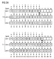
FIG 3 zeigt einen zur erfindungsgemäßen Datenratenanpassung verwendeten Zwischenspeicher mit beispielhafter Belegung. Der Zwischenspeicher ist dabei als FIFO-Speicher (First-In-First-Out, FIFO) ausgebildet und ist in der in FIG 1 dargestellten Einrichtung zur Takt- und Datenratenanpassung TRA1 angeordnet.FIG. 3 shows a data rate adaptation according to the invention used latches with exemplary occupancy. Of the Cache is a FIFO memory (First-In-First-Out, FIFO) and is shown in FIG Means arranged for clock and data rate adjustment TRA1.
Zusammengehörige Daten bzw. Einzeldatensignale eines parallelisierten
Datensignals werden mit identischen Buchstaben bezeichnet
und tragen zur Unterscheidbarkeit Nummern in aufsteigender
Reihenfolge. Der FIFO-Speicher weist im vorliegenden
Beispiel für 16 digitale Eingangsdatensignale insgesamt
fünfzehn Spalten Spalte 0 bis Spalte 14 und drei Zeilen Zeile
1 bis Zeile 3 auf. Related data or individual data signals of a parallelized
Data signals are denoted by identical letters
and bear numbers in ascending order for distinctness
Sequence. The FIFO memory has in the present
Example for 16 digital input data signals in total
fifteen columns,
Nachfolgend wird von folgendem Ablauf bei der Belegung des
Zwischenspeichers pro Takt ausgegangen:
In Zeile 3 sind Daten A7 bis A15 in Spalte 0 bis Spalte 8 abgelegt,
während Daten B0 bis B5 in Spalte 9 bis Spalte 14 abgelegt
sind.
In Zeile 2 sind Daten B6 bis B15 in Spalte 0 bis Spalte 9 abgelegt,
während neue Daten C0 bis C4 beginnend ab der Zeigerposition
in Spalte 10 bis Spalte 14 abgelegt werden.
In Zeile 1 werden neue Daten C5 bis C15 in Spalte 0 bis Spalte
10 abgelegt.In
In
In
Der Zeiger Z wird um eine Spalte nach rechts auf eine neue
Position in Zeile 2, Spalte 11, verschoben.The pointer Z is moved one column to the right to a new one
Position in
Nach einem Takt ändert sich der Speicherzustand T10 in den Speicherzustand T11. After one clock, the memory state T10 changes to Memory state T11.
Gemäß dem oben geschilderten Ablauf werden:
Nachfolgend wird von einem Pausentakt PT beim Übergang vom
Speicherzustand T11 in den Speicherzustand T12 ausgegangen.
Gemäß dem oben geschilderten Ablauf werden:
Beim Übergang vom Speicherzustand T12 in den Speicherzustand
T13 werden gemäß dem oben geschilderten Ablauf:
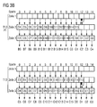
FIG 4 zeigt den Zwischenspeicher mit einer weiteren beispielhaften Belegung und mit zwei zur Datenratenanpassung eingeführten, zufällig aufeinanderfolgenden Pausentakten. Bei diesem Ausführungsbeispiel werden alle Speicherzellen des Zwischenspeichers verwendet.4 shows the buffer with a further exemplary Occupancy and with two introduced for data rate adjustment, randomly successive pause measures. In this Embodiment, all memory cells of the cache used.
Ein Taktzyklus weist jeweils 16 Takte auf. Die Speicherzustände T14 und T15 gehören zu den beiden letzten Takten eines ablaufenden Taktzyklus. Beim Speicherzustand T0 beginnt ein neuer Taktzyklus, wobei in jedem Taktzyklus genau einmal ein Pausentakt PT auftritt.One clock cycle has 16 clocks each. The memory states T14 and T15 belong to the last two bars of a expiring clock cycle. When memory state T0 starts on new clock cycle, with exactly one on each clock cycle Pausentakt PT occurs.
Im Folgenden wird davon ausgegangen, dass nach Ablauf einer
Anzahl an Taktzyklen bei einem Speicherzustand T14 der Zeiger
Z auf Zeile 2, Spalte 14, zeigt.In the following, it is assumed that after expiration of a
Number of clock cycles at a memory state T14 of the pointers
Z on
In Zeile 3 sind Daten A3 bis A15 in Spalte 0 bis Spalte 12
abgelegt, während Daten B0 und B1 in Spalte 13 und in Spalte
14 abgelegt sind.
In Zeile 2 sind Daten B2 bis B15 in Spalte 0 bis Spalte 13
abgelegt, während neue Daten C0 beginnend ab der Zeigerposition
in Spalte 14 abgelegt werden. In Zeile 1 werden neue Daten
C1 bis C15 in Spalte 0 bis Spalte 14 abgelegt.In
In
Der Zeiger Z wird um eine Spalte nach rechts auf eine neue
Position in Zeile 1, Spalte 0, verschoben.The pointer Z is moved one column to the right to a new one
Position in
Nachfolgen wird von einem Pausentakt PT beim Übergang vom Speicherzustand T14 in den Speicherzustand T15 ausgegangen. Followed by a pause clock PT at the transition from Memory state T14 went into the memory state T15.
Gemäß dem oben geschilderten Ablauf werden:
Nachfolgen wird von einem weiteren Pausentakt PT beim Übergang vom Speicherzustand T15 in den Speicherzustand T0 ausgegangen.Followed by another pause PT during the transition from memory state T15 into memory state T0.
Gemäß dem oben geschilderten Ablauf werden:
Beim Übergang vom Speicherzustand T0 in den Speicherzustand
T1 werden gemäß dem oben geschilderten Ablauf:
FIG 5 zeigt eine Anordnung zur Durchführung des erfindungsgemäßen Verfahrens mit einem mehrstufig ausgebildeten Demultiplexer.5 shows an arrangement for carrying out the inventive Method with a multistage demultiplexer.
Ein parallelisiertes Datensignal DS3 wird durch eine digitale Signalverarbeitungseinrichtung DSV3 gebildet. Das parallelisierte Datensignal DS3 weist insgesamt 16 zueinander parallel übertragene, digitale Einzeldatensignale D300 bis D315 auf, die an eine Einrichtung zur Takt- und Datenratenanpassung TRA3 gelangen. Die Einrichtung zur Takt- und Datenratenanpassung TRA3 bildet die insgesamt 16 Einzeldatensignale D300 bis D315 auf insgesamt 15 Einzeldatensignale D400 bis D414 ab.A parallelized data signal DS3 is by a digital Signal processing device DSV3 formed. The parallelized Data signal DS3 has a total of 16 parallel to each other transmitted digital single data signals D300 to D315 on, to a device for clock and data rate adaptation TRA3 arrive. The device for clock and data rate adaptation TRA3 forms the total of 16 individual data signals D300 to D315 to a total of 15 individual data signals D400 to D414 from.
Die 15 Einzeldatensignale D400 bis D414 bilden wiederum ein parallelisiertes Datensignal DS4, das an einen als Demultiplexer DEMUX3 ausgebildeten Parallel-Parallel-Wandler PPW3 gelangt. Dieser bildet aus den 15 Einzeldatensignalen D400 bis D414 ein insgesamt drei Einzeldatensignale D500 bis D502 aufweisendes parallelisiertes Datensignal DS5 mit der Taktfrequenz fCLK/3, das an einen als Demultiplexer DEMUX4 ausgebildeten Parallel-Seriell-Wandler PSW4 gelangt. Dieser bildet ein serielles digitales Ausgangsdatensignal DOUT3.The 15 individual data signals D400 to D414 form again parallelized data signal DS4, the one as a demultiplexer DEMUX3 trained parallel-parallel converter PPW3 arrives. This forms from the 15 individual data signals D400 to D414 a total of three individual data signals D500 to D502 having parallelized data signal DS5 with the clock frequency fCLK / 3, which is designed as a demultiplexer DEMUX4 Parallel-serial converter PSW4 arrives. This forms a serial digital output data signal DOUT3.
Mit Hilfe der Einrichtung zur Takt- und Datenratenanpassung TRA3 erfolgt eine Anpassung der Datenrate von 16:15, während mit Hilfe des Demultiplexers DEMUX3 eine Anpassung der Datenrate von 15:3 durchgeführt wird.With the help of the device for clock and data rate adjustment TRA3 will adjust the data rate from 16:15 while with the help of the demultiplexer DEMUX3 an adjustment of the data rate of 15: 3 is performed.
Erfindungsgemäß wird bei der Umsetzung der jeweiligen parallelisierten
Datensignale der Faktor 4 in den jeweiligen Teilerverhältnissen
vermieden.According to the invention is parallelized in the implementation of the respective
Data signals of
Außerdem können beide (Takt-)Teilerverhältnisse mit 5:1 und mit 3:1 relativ klein gewählt werden, da das Gesamtteilerverhältnis 15:1 keine großen Primfaktoren enthält. In addition, both (clock) divider ratios with 5: 1 and with 3: 1 are chosen to be relatively small, since the overall divider ratio 15: 1 does not contain large prime factors.
Die Größe des sowohl in FIG 1 als auch in FIG 5 jeweils benötigten
Zwischenspeichers wächst zunächst mit größer werdender
Differenz zwischen den Teilerverhältnissen NpL und NpL' an
und errechnet sich zu:
mit (1+2*(NpL-NpL') als Zeilenanzahl.The size of the temporary storage required in each case in FIG. 1 as well as in FIG. 5 initially grows with increasing difference between the division ratios NpL and NpL 'and is calculated as:
with (1 + 2 * (NpL-NpL ') as the number of lines.
Mit den Werten aus FIG 1 ergibt sich eine Puffergröße des
Zwischenspeichers von:
Es ist jedoch auch möglich, durch Einschränkungen bei der Pausenwahl einen Zwischenspeicher mit einer geringeren Kapazität zu verwenden.However, it is also possible through limitations in the Pause a cache with a smaller capacity to use.
Weiter könnte die letzte Zeile des Zwischenspeichers ohne
Einschränkung bei der Pausenwahl dann entfallen, wenn mit
Hilfe des Zeigers Z direkt auf den Ausgang zugegriffen wird.
Die letzte Zeile des Zwischenspeichers wäre dann als parallele
Ausgangsleitung ausgebildet. Damit ergäbe sich die Puffergröße
wie folgt:
Das Teilerverhältnis NpL' wird bevorzugt derart gewählt, dass es keine großen Primfaktoren aufweist, um den Aufwand bei der Parallel-Seriell-Wandlung zu minimieren.The divider ratio NpL 'is preferably selected such that it does not have large prime factors to reduce the overhead of the Minimize parallel-to-serial conversion.
Zweckmäßigerweise wird das Teilerverhältnis NpL' beginnend
bei NpL-1 bis zu einem Wert schrittweise verringert, der weder
den Faktor 4 ganzzahlig beinhaltet und idealerweise keinen
zu großen Primfaktor aufweist. Conveniently, the divider ratio NpL 'starting
at NpL-1, gradually decreasing to a value that neither
contains the
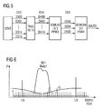
FIG 6 zeigt einen Teilbereich des in FIG 2 dargestellten Frequenzspektrums mit Störsignalen beim Teilerverhältnis NpL'= 15.6 shows a partial region of the frequency spectrum shown in FIG with interference signals at the divider ratio NpL '= 15.
Zum Vergleich sind subharmonische Störlinien SL mit Oberwellen eingetragen, die bei regelmäßig auftretenden Pausentakten entstehen würden. Durch das erfindungsgemäße unregelmäßige Auftreten des Pausentakts hingegen entstehen keine subharmonischen Störlinien, da deren Energie E gleichmäßig im gesamten Frequenzspektrum verteilt wird, hier schraffiert dargestellt. Somit wird der Spitzenstörpegel abgesenkt.For comparison, subharmonic interference lines SL with harmonics registered, which occurs regularly with pauses would arise. By the inventive irregular On the other hand, there are no subharmonic occurrences of the pause cycle Interference, because their energy E uniform throughout Frequency spectrum is distributed, shown here hatched. Thus, the peak noise level is lowered.
Claims (11)
Priority Applications (1)
| Application Number | Priority Date | Filing Date | Title |
|---|---|---|---|
| EP03026763.7A EP1533962B1 (en) | 2003-11-21 | 2003-11-21 | Method and arrangement for suppressing interferences in the useful frequency band of an analog output signal |
Applications Claiming Priority (1)
| Application Number | Priority Date | Filing Date | Title |
|---|---|---|---|
| EP03026763.7A EP1533962B1 (en) | 2003-11-21 | 2003-11-21 | Method and arrangement for suppressing interferences in the useful frequency band of an analog output signal |
Publications (2)
| Publication Number | Publication Date |
|---|---|
| EP1533962A1 true EP1533962A1 (en) | 2005-05-25 |
| EP1533962B1 EP1533962B1 (en) | 2015-11-11 |
Family
ID=34429410
Family Applications (1)
| Application Number | Title | Priority Date | Filing Date |
|---|---|---|---|
| EP03026763.7A Expired - Lifetime EP1533962B1 (en) | 2003-11-21 | 2003-11-21 | Method and arrangement for suppressing interferences in the useful frequency band of an analog output signal |
Country Status (1)
| Country | Link |
|---|---|
| EP (1) | EP1533962B1 (en) |
Cited By (1)
| Publication number | Priority date | Publication date | Assignee | Title |
|---|---|---|---|---|
| EP1868313A2 (en) * | 2006-06-14 | 2007-12-19 | Siemens Aktiengesellschaft | Method for data transmission between a mounting head control device and a central control device in a mounting machine, mounting machine, mounting head, sender-side transmission device and system consisting of sender-side and receiver-side transmission device |
Citations (3)
| Publication number | Priority date | Publication date | Assignee | Title |
|---|---|---|---|---|
| EP0092083A2 (en) * | 1982-04-17 | 1983-10-26 | Neumann Elektronik GmbH | Electronic message sender for transmitting and/or recording messages on a telephone line |
| US4868572A (en) * | 1987-02-28 | 1989-09-19 | Alcatel N.V. | Circuit arrangement for converting digital sound-signal values into an analog sound signal |
| US5555447A (en) * | 1993-05-14 | 1996-09-10 | Motorola, Inc. | Method and apparatus for mitigating speech loss in a communication system |
-
2003
- 2003-11-21 EP EP03026763.7A patent/EP1533962B1/en not_active Expired - Lifetime
Patent Citations (3)
| Publication number | Priority date | Publication date | Assignee | Title |
|---|---|---|---|---|
| EP0092083A2 (en) * | 1982-04-17 | 1983-10-26 | Neumann Elektronik GmbH | Electronic message sender for transmitting and/or recording messages on a telephone line |
| US4868572A (en) * | 1987-02-28 | 1989-09-19 | Alcatel N.V. | Circuit arrangement for converting digital sound-signal values into an analog sound signal |
| US5555447A (en) * | 1993-05-14 | 1996-09-10 | Motorola, Inc. | Method and apparatus for mitigating speech loss in a communication system |
Non-Patent Citations (2)
| Title |
|---|
| CAO J ET AL: "OC-192 transmitter and receiver in standard 0.18- mu m CMOS", IEEE JOURNAL OF SOLID-STATE CIRCUITS, vol. 37, no. 12, December 2002 (2002-12-01), IEEE,USA, pages 1768 - 1780, XP002288148, ISSN: 0018-9200 * |
| KAWAI T ET AL: "CROSSTALK REDUCTION IN N X N WDM MULTI/DEMULTIPLEXERS BY CASCADING SMALL ARRAYED WAVEGUIDE GRATING (AWG'S)", JOURNAL OF LIGHTWAVE TECHNOLOGY, vol. 15, no. 10, 1 October 1997 (1997-10-01), IEEE, NEW YORK, US, pages 1929 - 1937, XP000703612, ISSN: 0733-8724 * |
Cited By (2)
| Publication number | Priority date | Publication date | Assignee | Title |
|---|---|---|---|---|
| EP1868313A2 (en) * | 2006-06-14 | 2007-12-19 | Siemens Aktiengesellschaft | Method for data transmission between a mounting head control device and a central control device in a mounting machine, mounting machine, mounting head, sender-side transmission device and system consisting of sender-side and receiver-side transmission device |
| EP1868313A3 (en) * | 2006-06-14 | 2008-05-21 | Siemens Aktiengesellschaft | Method for data transmission between a mounting head control device and a central control device in a mounting machine, mounting machine, mounting head, sender-side transmission device and system consisting of sender-side and receiver-side transmission device |
Also Published As
| Publication number | Publication date |
|---|---|
| EP1533962B1 (en) | 2015-11-11 |
Similar Documents
| Publication | Publication Date | Title |
|---|---|---|
| DE3044208C2 (en) | Interpolator for increasing the word speed of a digital signal | |
| DE69817270T2 (en) | Arrangement for the generation of analog signals using analog-digital converters, especially for direct digital synthesis | |
| DE4241882A1 (en) | ||
| DE2605724C2 (en) | Digital-to-analog converter for PCM-coded digital signals | |
| EP0691756A1 (en) | Echo canceller with analogue coarse canceller and digital fine canceller | |
| DE102005030563B4 (en) | Multichannel digital / analog converter arrangement | |
| DE10325839B4 (en) | Method and circuit for crest factor reduction | |
| DE3813068C2 (en) | Device for use as a filter in a digital / analog converter | |
| DE4325728A1 (en) | Noise reduction for a synthesis based on several modulators | |
| EP0732823B1 (en) | Method for clock recovery of a digital signal on the reception side | |
| EP0135066B1 (en) | Transfer device for digital signals | |
| DE3044582A1 (en) | DIGITAL AMPLIFIER, ESPECIALLY FOR USE IN A DIGITAL TELEPHONE PARTICIPANT CIRCUIT | |
| DE3033914A1 (en) | DIGITAL / ANALOG CONVERTER AND PCM CODER THEREFOR. | |
| EP1533962B1 (en) | Method and arrangement for suppressing interferences in the useful frequency band of an analog output signal | |
| EP0340301B1 (en) | Digital adaptive transform coding process | |
| DE2229398A1 (en) | Differential pulse code modulation system with periodic change in the modulator step | |
| DE2633420A1 (en) | METHOD AND EQUIPMENT FOR BINARY EQUALIZATION FOR MODEMS WITH PHASE-MODULATED CARRIER FROM THE VOICE RIBBON | |
| DE4036972A1 (en) | Digital audio signal receiver - includes circuit removing modulation noise by adjusting duty rate to provide original PCM signal | |
| DE2231083C3 (en) | Device for generating tones of a musical scale | |
| DE2011772B2 (en) | FILTER WITH PERIODIC FREQUENCY CHARACTERISTICS | |
| DE2827958B1 (en) | Section regenerator for multi-level digital signals in a partial response code | |
| DE10112275A1 (en) | interpolator | |
| EP0477131B1 (en) | Method and apparatus for sample rate conversion | |
| EP0028405A2 (en) | Method and arrangement for reducing jitter during block transcoding of digital signals | |
| DE69734770T2 (en) | Sample rate conversion with distributed decimation |
Legal Events
| Date | Code | Title | Description |
|---|---|---|---|
| PUAI | Public reference made under article 153(3) epc to a published international application that has entered the european phase |
Free format text: ORIGINAL CODE: 0009012 |
|
| AK | Designated contracting states |
Kind code of ref document: A1 Designated state(s): AT BE BG CH CY CZ DE DK EE ES FI FR GB GR HU IE IT LI LU MC NL PT RO SE SI SK TR |
|
| AX | Request for extension of the european patent |
Extension state: AL LT LV MK |
|
| 17P | Request for examination filed |
Effective date: 20050620 |
|
| AKX | Designation fees paid |
Designated state(s): AT BE BG CH CY CZ DE DK EE ES FI FR GB GR HU IE IT LI LU MC NL PT RO SE SI SK TR |
|
| RAP1 | Party data changed (applicant data changed or rights of an application transferred) |
Owner name: NOKIA SIEMENS NETWORKS GMBH & CO. KG |
|
| RAP3 | Party data changed (applicant data changed or rights of an application transferred) |
Owner name: NOKIA SIEMENS NETWORKS S.P.A. |
|
| RAP3 | Party data changed (applicant data changed or rights of an application transferred) |
Owner name: NOKIA SIEMENS NETWORKS GMBH & CO. KG |
|
| RAP1 | Party data changed (applicant data changed or rights of an application transferred) |
Owner name: NOKIA SOLUTIONS AND NETWORKS GMBH & CO. KG |
|
| GRAP | Despatch of communication of intention to grant a patent |
Free format text: ORIGINAL CODE: EPIDOSNIGR1 |
|
| INTG | Intention to grant announced |
Effective date: 20150611 |
|
| GRAS | Grant fee paid |
Free format text: ORIGINAL CODE: EPIDOSNIGR3 |
|
| GRAA | (expected) grant |
Free format text: ORIGINAL CODE: 0009210 |
|
| AK | Designated contracting states |
Kind code of ref document: B1 Designated state(s): AT BE BG CH CY CZ DE DK EE ES FI FR GB GR HU IE IT LI LU MC NL PT RO SE SI SK TR |
|
| REG | Reference to a national code |
Ref country code: GB Ref legal event code: FG4D Free format text: NOT ENGLISH |
|
| REG | Reference to a national code |
Ref country code: CH Ref legal event code: EP |
|
| REG | Reference to a national code |
Ref country code: IE Ref legal event code: FG4D Free format text: LANGUAGE OF EP DOCUMENT: GERMAN |
|
| REG | Reference to a national code |
Ref country code: AT Ref legal event code: REF Ref document number: 760934 Country of ref document: AT Kind code of ref document: T Effective date: 20151215 |
|
| REG | Reference to a national code |
Ref country code: DE Ref legal event code: R096 Ref document number: 50315374 Country of ref document: DE |
|
| REG | Reference to a national code |
Ref country code: NL Ref legal event code: MP Effective date: 20160211 |
|
| PG25 | Lapsed in a contracting state [announced via postgrant information from national office to epo] |
Ref country code: IT Free format text: LAPSE BECAUSE OF FAILURE TO SUBMIT A TRANSLATION OF THE DESCRIPTION OR TO PAY THE FEE WITHIN THE PRESCRIBED TIME-LIMIT Effective date: 20151111 Ref country code: NL Free format text: LAPSE BECAUSE OF FAILURE TO SUBMIT A TRANSLATION OF THE DESCRIPTION OR TO PAY THE FEE WITHIN THE PRESCRIBED TIME-LIMIT Effective date: 20151111 Ref country code: ES Free format text: LAPSE BECAUSE OF FAILURE TO SUBMIT A TRANSLATION OF THE DESCRIPTION OR TO PAY THE FEE WITHIN THE PRESCRIBED TIME-LIMIT Effective date: 20151111 |
|
| PG25 | Lapsed in a contracting state [announced via postgrant information from national office to epo] |
Ref country code: SE Free format text: LAPSE BECAUSE OF FAILURE TO SUBMIT A TRANSLATION OF THE DESCRIPTION OR TO PAY THE FEE WITHIN THE PRESCRIBED TIME-LIMIT Effective date: 20151111 Ref country code: FI Free format text: LAPSE BECAUSE OF FAILURE TO SUBMIT A TRANSLATION OF THE DESCRIPTION OR TO PAY THE FEE WITHIN THE PRESCRIBED TIME-LIMIT Effective date: 20151111 Ref country code: PT Free format text: LAPSE BECAUSE OF FAILURE TO SUBMIT A TRANSLATION OF THE DESCRIPTION OR TO PAY THE FEE WITHIN THE PRESCRIBED TIME-LIMIT Effective date: 20160311 Ref country code: GR Free format text: LAPSE BECAUSE OF FAILURE TO SUBMIT A TRANSLATION OF THE DESCRIPTION OR TO PAY THE FEE WITHIN THE PRESCRIBED TIME-LIMIT Effective date: 20160212 Ref country code: BE Free format text: LAPSE BECAUSE OF NON-PAYMENT OF DUE FEES Effective date: 20151130 |
|
| REG | Reference to a national code |
Ref country code: CH Ref legal event code: PL |
|
| PG25 | Lapsed in a contracting state [announced via postgrant information from national office to epo] |
Ref country code: CH Free format text: LAPSE BECAUSE OF NON-PAYMENT OF DUE FEES Effective date: 20151130 Ref country code: CZ Free format text: LAPSE BECAUSE OF FAILURE TO SUBMIT A TRANSLATION OF THE DESCRIPTION OR TO PAY THE FEE WITHIN THE PRESCRIBED TIME-LIMIT Effective date: 20151111 Ref country code: LI Free format text: LAPSE BECAUSE OF NON-PAYMENT OF DUE FEES Effective date: 20151130 |
|
| REG | Reference to a national code |
Ref country code: DE Ref legal event code: R097 Ref document number: 50315374 Country of ref document: DE |
|
| REG | Reference to a national code |
Ref country code: IE Ref legal event code: MM4A |
|
| PG25 | Lapsed in a contracting state [announced via postgrant information from national office to epo] |
Ref country code: SK Free format text: LAPSE BECAUSE OF FAILURE TO SUBMIT A TRANSLATION OF THE DESCRIPTION OR TO PAY THE FEE WITHIN THE PRESCRIBED TIME-LIMIT Effective date: 20151111 Ref country code: RO Free format text: LAPSE BECAUSE OF FAILURE TO SUBMIT A TRANSLATION OF THE DESCRIPTION OR TO PAY THE FEE WITHIN THE PRESCRIBED TIME-LIMIT Effective date: 20151111 Ref country code: DK Free format text: LAPSE BECAUSE OF FAILURE TO SUBMIT A TRANSLATION OF THE DESCRIPTION OR TO PAY THE FEE WITHIN THE PRESCRIBED TIME-LIMIT Effective date: 20151111 Ref country code: EE Free format text: LAPSE BECAUSE OF FAILURE TO SUBMIT A TRANSLATION OF THE DESCRIPTION OR TO PAY THE FEE WITHIN THE PRESCRIBED TIME-LIMIT Effective date: 20151111 |
|
| PLBE | No opposition filed within time limit |
Free format text: ORIGINAL CODE: 0009261 |
|
| STAA | Information on the status of an ep patent application or granted ep patent |
Free format text: STATUS: NO OPPOSITION FILED WITHIN TIME LIMIT |
|
| PG25 | Lapsed in a contracting state [announced via postgrant information from national office to epo] |
Ref country code: MC Free format text: LAPSE BECAUSE OF FAILURE TO SUBMIT A TRANSLATION OF THE DESCRIPTION OR TO PAY THE FEE WITHIN THE PRESCRIBED TIME-LIMIT Effective date: 20151111 |
|
| 26N | No opposition filed |
Effective date: 20160812 |
|
| PG25 | Lapsed in a contracting state [announced via postgrant information from national office to epo] |
Ref country code: IE Free format text: LAPSE BECAUSE OF NON-PAYMENT OF DUE FEES Effective date: 20151121 |
|
| REG | Reference to a national code |
Ref country code: FR Ref legal event code: ST Effective date: 20161003 |
|
| PG25 | Lapsed in a contracting state [announced via postgrant information from national office to epo] |
Ref country code: FR Free format text: LAPSE BECAUSE OF NON-PAYMENT OF DUE FEES Effective date: 20160111 Ref country code: SI Free format text: LAPSE BECAUSE OF FAILURE TO SUBMIT A TRANSLATION OF THE DESCRIPTION OR TO PAY THE FEE WITHIN THE PRESCRIBED TIME-LIMIT Effective date: 20151111 |
|
| REG | Reference to a national code |
Ref country code: AT Ref legal event code: MM01 Ref document number: 760934 Country of ref document: AT Kind code of ref document: T Effective date: 20151121 |
|
| PG25 | Lapsed in a contracting state [announced via postgrant information from national office to epo] |
Ref country code: AT Free format text: LAPSE BECAUSE OF NON-PAYMENT OF DUE FEES Effective date: 20151121 |
|
| PG25 | Lapsed in a contracting state [announced via postgrant information from national office to epo] |
Ref country code: HU Free format text: LAPSE BECAUSE OF FAILURE TO SUBMIT A TRANSLATION OF THE DESCRIPTION OR TO PAY THE FEE WITHIN THE PRESCRIBED TIME-LIMIT; INVALID AB INITIO Effective date: 20031121 Ref country code: BG Free format text: LAPSE BECAUSE OF FAILURE TO SUBMIT A TRANSLATION OF THE DESCRIPTION OR TO PAY THE FEE WITHIN THE PRESCRIBED TIME-LIMIT Effective date: 20151111 |
|
| PG25 | Lapsed in a contracting state [announced via postgrant information from national office to epo] |
Ref country code: CY Free format text: LAPSE BECAUSE OF FAILURE TO SUBMIT A TRANSLATION OF THE DESCRIPTION OR TO PAY THE FEE WITHIN THE PRESCRIBED TIME-LIMIT Effective date: 20151111 |
|
| PG25 | Lapsed in a contracting state [announced via postgrant information from national office to epo] |
Ref country code: TR Free format text: LAPSE BECAUSE OF FAILURE TO SUBMIT A TRANSLATION OF THE DESCRIPTION OR TO PAY THE FEE WITHIN THE PRESCRIBED TIME-LIMIT Effective date: 20151111 |
|
| PG25 | Lapsed in a contracting state [announced via postgrant information from national office to epo] |
Ref country code: LU Free format text: LAPSE BECAUSE OF NON-PAYMENT OF DUE FEES Effective date: 20151121 |
|
| PGFP | Annual fee paid to national office [announced via postgrant information from national office to epo] |
Ref country code: DE Payment date: 20171121 Year of fee payment: 15 |
|
| PGFP | Annual fee paid to national office [announced via postgrant information from national office to epo] |
Ref country code: GB Payment date: 20171123 Year of fee payment: 15 |
|
| REG | Reference to a national code |
Ref country code: GB Ref legal event code: 732E Free format text: REGISTERED BETWEEN 20190207 AND 20190213 |
|
| REG | Reference to a national code |
Ref country code: DE Ref legal event code: R081 Ref document number: 50315374 Country of ref document: DE Owner name: PROVENANCE ASSET GROUP LLC, PITTSFORD, US Free format text: FORMER OWNER: NOKIA SOLUTIONS AND NETWORKS GMBH & CO. KG, 81541 MUENCHEN, DE |
|
| REG | Reference to a national code |
Ref country code: DE Ref legal event code: R119 Ref document number: 50315374 Country of ref document: DE |
|
| GBPC | Gb: european patent ceased through non-payment of renewal fee |
Effective date: 20181121 |
|
| PG25 | Lapsed in a contracting state [announced via postgrant information from national office to epo] |
Ref country code: DE Free format text: LAPSE BECAUSE OF NON-PAYMENT OF DUE FEES Effective date: 20190601 |
|
| PG25 | Lapsed in a contracting state [announced via postgrant information from national office to epo] |
Ref country code: GB Free format text: LAPSE BECAUSE OF NON-PAYMENT OF DUE FEES Effective date: 20181121 |