EP1513235A1 - VCSEL with monolithically integrated photodetector and hybrid mirrors - Google Patents
VCSEL with monolithically integrated photodetector and hybrid mirrors Download PDFInfo
- Publication number
- EP1513235A1 EP1513235A1 EP04018720A EP04018720A EP1513235A1 EP 1513235 A1 EP1513235 A1 EP 1513235A1 EP 04018720 A EP04018720 A EP 04018720A EP 04018720 A EP04018720 A EP 04018720A EP 1513235 A1 EP1513235 A1 EP 1513235A1
- Authority
- EP
- European Patent Office
- Prior art keywords
- section
- electrode
- region
- laser
- ses
- Prior art date
- Legal status (The legal status is an assumption and is not a legal conclusion. Google has not performed a legal analysis and makes no representation as to the accuracy of the status listed.)
- Granted
Links
Images


Classifications
-
- H—ELECTRICITY
- H01—ELECTRIC ELEMENTS
- H01S—DEVICES USING THE PROCESS OF LIGHT AMPLIFICATION BY STIMULATED EMISSION OF RADIATION [LASER] TO AMPLIFY OR GENERATE LIGHT; DEVICES USING STIMULATED EMISSION OF ELECTROMAGNETIC RADIATION IN WAVE RANGES OTHER THAN OPTICAL
- H01S5/00—Semiconductor lasers
- H01S5/10—Construction or shape of the optical resonator, e.g. extended or external cavity, coupled cavities, bent-guide, varying width, thickness or composition of the active region
- H01S5/18—Surface-emitting [SE] lasers, e.g. having both horizontal and vertical cavities
- H01S5/183—Surface-emitting [SE] lasers, e.g. having both horizontal and vertical cavities having only vertical cavities, e.g. vertical cavity surface-emitting lasers [VCSEL]
- H01S5/18341—Intra-cavity contacts
-
- H—ELECTRICITY
- H01—ELECTRIC ELEMENTS
- H01S—DEVICES USING THE PROCESS OF LIGHT AMPLIFICATION BY STIMULATED EMISSION OF RADIATION [LASER] TO AMPLIFY OR GENERATE LIGHT; DEVICES USING STIMULATED EMISSION OF ELECTROMAGNETIC RADIATION IN WAVE RANGES OTHER THAN OPTICAL
- H01S5/00—Semiconductor lasers
- H01S5/02—Structural details or components not essential to laser action
- H01S5/026—Monolithically integrated components, e.g. waveguides, monitoring photo-detectors, drivers
- H01S5/0262—Photo-diodes, e.g. transceiver devices, bidirectional devices
- H01S5/0264—Photo-diodes, e.g. transceiver devices, bidirectional devices for monitoring the laser-output
-
- H—ELECTRICITY
- H01—ELECTRIC ELEMENTS
- H01S—DEVICES USING THE PROCESS OF LIGHT AMPLIFICATION BY STIMULATED EMISSION OF RADIATION [LASER] TO AMPLIFY OR GENERATE LIGHT; DEVICES USING STIMULATED EMISSION OF ELECTROMAGNETIC RADIATION IN WAVE RANGES OTHER THAN OPTICAL
- H01S5/00—Semiconductor lasers
- H01S5/04—Processes or apparatus for excitation, e.g. pumping, e.g. by electron beams
- H01S5/042—Electrical excitation ; Circuits therefor
- H01S5/0425—Electrodes, e.g. characterised by the structure
-
- H—ELECTRICITY
- H01—ELECTRIC ELEMENTS
- H01L—SEMICONDUCTOR DEVICES NOT COVERED BY CLASS H10
- H01L2224/00—Indexing scheme for arrangements for connecting or disconnecting semiconductor or solid-state bodies and methods related thereto as covered by H01L24/00
- H01L2224/01—Means for bonding being attached to, or being formed on, the surface to be connected, e.g. chip-to-package, die-attach, "first-level" interconnects; Manufacturing methods related thereto
- H01L2224/10—Bump connectors; Manufacturing methods related thereto
- H01L2224/15—Structure, shape, material or disposition of the bump connectors after the connecting process
- H01L2224/16—Structure, shape, material or disposition of the bump connectors after the connecting process of an individual bump connector
- H01L2224/161—Disposition
- H01L2224/16135—Disposition the bump connector connecting between different semiconductor or solid-state bodies, i.e. chip-to-chip
- H01L2224/16145—Disposition the bump connector connecting between different semiconductor or solid-state bodies, i.e. chip-to-chip the bodies being stacked
-
- H—ELECTRICITY
- H01—ELECTRIC ELEMENTS
- H01L—SEMICONDUCTOR DEVICES NOT COVERED BY CLASS H10
- H01L2224/00—Indexing scheme for arrangements for connecting or disconnecting semiconductor or solid-state bodies and methods related thereto as covered by H01L24/00
- H01L2224/01—Means for bonding being attached to, or being formed on, the surface to be connected, e.g. chip-to-package, die-attach, "first-level" interconnects; Manufacturing methods related thereto
- H01L2224/42—Wire connectors; Manufacturing methods related thereto
- H01L2224/47—Structure, shape, material or disposition of the wire connectors after the connecting process
- H01L2224/48—Structure, shape, material or disposition of the wire connectors after the connecting process of an individual wire connector
- H01L2224/4805—Shape
- H01L2224/4809—Loop shape
- H01L2224/48091—Arched
-
- H—ELECTRICITY
- H01—ELECTRIC ELEMENTS
- H01L—SEMICONDUCTOR DEVICES NOT COVERED BY CLASS H10
- H01L2224/00—Indexing scheme for arrangements for connecting or disconnecting semiconductor or solid-state bodies and methods related thereto as covered by H01L24/00
- H01L2224/01—Means for bonding being attached to, or being formed on, the surface to be connected, e.g. chip-to-package, die-attach, "first-level" interconnects; Manufacturing methods related thereto
- H01L2224/42—Wire connectors; Manufacturing methods related thereto
- H01L2224/47—Structure, shape, material or disposition of the wire connectors after the connecting process
- H01L2224/48—Structure, shape, material or disposition of the wire connectors after the connecting process of an individual wire connector
- H01L2224/481—Disposition
- H01L2224/48151—Connecting between a semiconductor or solid-state body and an item not being a semiconductor or solid-state body, e.g. chip-to-substrate, chip-to-passive
- H01L2224/48221—Connecting between a semiconductor or solid-state body and an item not being a semiconductor or solid-state body, e.g. chip-to-substrate, chip-to-passive the body and the item being stacked
- H01L2224/48225—Connecting between a semiconductor or solid-state body and an item not being a semiconductor or solid-state body, e.g. chip-to-substrate, chip-to-passive the body and the item being stacked the item being non-metallic, e.g. insulating substrate with or without metallisation
- H01L2224/48227—Connecting between a semiconductor or solid-state body and an item not being a semiconductor or solid-state body, e.g. chip-to-substrate, chip-to-passive the body and the item being stacked the item being non-metallic, e.g. insulating substrate with or without metallisation connecting the wire to a bond pad of the item
-
- H—ELECTRICITY
- H01—ELECTRIC ELEMENTS
- H01L—SEMICONDUCTOR DEVICES NOT COVERED BY CLASS H10
- H01L2224/00—Indexing scheme for arrangements for connecting or disconnecting semiconductor or solid-state bodies and methods related thereto as covered by H01L24/00
- H01L2224/01—Means for bonding being attached to, or being formed on, the surface to be connected, e.g. chip-to-package, die-attach, "first-level" interconnects; Manufacturing methods related thereto
- H01L2224/42—Wire connectors; Manufacturing methods related thereto
- H01L2224/47—Structure, shape, material or disposition of the wire connectors after the connecting process
- H01L2224/48—Structure, shape, material or disposition of the wire connectors after the connecting process of an individual wire connector
- H01L2224/484—Connecting portions
- H01L2224/48463—Connecting portions the connecting portion on the bonding area of the semiconductor or solid-state body being a ball bond
- H01L2224/48464—Connecting portions the connecting portion on the bonding area of the semiconductor or solid-state body being a ball bond the other connecting portion not on the bonding area also being a ball bond, i.e. ball-to-ball
-
- H—ELECTRICITY
- H01—ELECTRIC ELEMENTS
- H01L—SEMICONDUCTOR DEVICES NOT COVERED BY CLASS H10
- H01L2224/00—Indexing scheme for arrangements for connecting or disconnecting semiconductor or solid-state bodies and methods related thereto as covered by H01L24/00
- H01L2224/73—Means for bonding being of different types provided for in two or more of groups H01L2224/10, H01L2224/18, H01L2224/26, H01L2224/34, H01L2224/42, H01L2224/50, H01L2224/63, H01L2224/71
- H01L2224/732—Location after the connecting process
- H01L2224/73251—Location after the connecting process on different surfaces
- H01L2224/73265—Layer and wire connectors
-
- H—ELECTRICITY
- H01—ELECTRIC ELEMENTS
- H01L—SEMICONDUCTOR DEVICES NOT COVERED BY CLASS H10
- H01L2924/00—Indexing scheme for arrangements or methods for connecting or disconnecting semiconductor or solid-state bodies as covered by H01L24/00
- H01L2924/15—Details of package parts other than the semiconductor or other solid state devices to be connected
- H01L2924/181—Encapsulation
-
- H—ELECTRICITY
- H01—ELECTRIC ELEMENTS
- H01S—DEVICES USING THE PROCESS OF LIGHT AMPLIFICATION BY STIMULATED EMISSION OF RADIATION [LASER] TO AMPLIFY OR GENERATE LIGHT; DEVICES USING STIMULATED EMISSION OF ELECTROMAGNETIC RADIATION IN WAVE RANGES OTHER THAN OPTICAL
- H01S2301/00—Functional characteristics
- H01S2301/17—Semiconductor lasers comprising special layers
- H01S2301/176—Specific passivation layers on surfaces other than the emission facet
-
- H—ELECTRICITY
- H01—ELECTRIC ELEMENTS
- H01S—DEVICES USING THE PROCESS OF LIGHT AMPLIFICATION BY STIMULATED EMISSION OF RADIATION [LASER] TO AMPLIFY OR GENERATE LIGHT; DEVICES USING STIMULATED EMISSION OF ELECTROMAGNETIC RADIATION IN WAVE RANGES OTHER THAN OPTICAL
- H01S5/00—Semiconductor lasers
- H01S5/02—Structural details or components not essential to laser action
- H01S5/022—Mountings; Housings
- H01S5/0225—Out-coupling of light
- H01S5/02251—Out-coupling of light using optical fibres
-
- H—ELECTRICITY
- H01—ELECTRIC ELEMENTS
- H01S—DEVICES USING THE PROCESS OF LIGHT AMPLIFICATION BY STIMULATED EMISSION OF RADIATION [LASER] TO AMPLIFY OR GENERATE LIGHT; DEVICES USING STIMULATED EMISSION OF ELECTROMAGNETIC RADIATION IN WAVE RANGES OTHER THAN OPTICAL
- H01S5/00—Semiconductor lasers
- H01S5/02—Structural details or components not essential to laser action
- H01S5/022—Mountings; Housings
- H01S5/0235—Method for mounting laser chips
- H01S5/02355—Fixing laser chips on mounts
- H01S5/0237—Fixing laser chips on mounts by soldering
-
- H—ELECTRICITY
- H01—ELECTRIC ELEMENTS
- H01S—DEVICES USING THE PROCESS OF LIGHT AMPLIFICATION BY STIMULATED EMISSION OF RADIATION [LASER] TO AMPLIFY OR GENERATE LIGHT; DEVICES USING STIMULATED EMISSION OF ELECTROMAGNETIC RADIATION IN WAVE RANGES OTHER THAN OPTICAL
- H01S5/00—Semiconductor lasers
- H01S5/04—Processes or apparatus for excitation, e.g. pumping, e.g. by electron beams
- H01S5/042—Electrical excitation ; Circuits therefor
- H01S5/0425—Electrodes, e.g. characterised by the structure
- H01S5/04256—Electrodes, e.g. characterised by the structure characterised by the configuration
- H01S5/04257—Electrodes, e.g. characterised by the structure characterised by the configuration having positive and negative electrodes on the same side of the substrate
-
- H—ELECTRICITY
- H01—ELECTRIC ELEMENTS
- H01S—DEVICES USING THE PROCESS OF LIGHT AMPLIFICATION BY STIMULATED EMISSION OF RADIATION [LASER] TO AMPLIFY OR GENERATE LIGHT; DEVICES USING STIMULATED EMISSION OF ELECTROMAGNETIC RADIATION IN WAVE RANGES OTHER THAN OPTICAL
- H01S5/00—Semiconductor lasers
- H01S5/10—Construction or shape of the optical resonator, e.g. extended or external cavity, coupled cavities, bent-guide, varying width, thickness or composition of the active region
- H01S5/18—Surface-emitting [SE] lasers, e.g. having both horizontal and vertical cavities
- H01S5/183—Surface-emitting [SE] lasers, e.g. having both horizontal and vertical cavities having only vertical cavities, e.g. vertical cavity surface-emitting lasers [VCSEL]
- H01S5/18308—Surface-emitting [SE] lasers, e.g. having both horizontal and vertical cavities having only vertical cavities, e.g. vertical cavity surface-emitting lasers [VCSEL] having a special structure for lateral current or light confinement
- H01S5/18311—Surface-emitting [SE] lasers, e.g. having both horizontal and vertical cavities having only vertical cavities, e.g. vertical cavity surface-emitting lasers [VCSEL] having a special structure for lateral current or light confinement using selective oxidation
- H01S5/18313—Surface-emitting [SE] lasers, e.g. having both horizontal and vertical cavities having only vertical cavities, e.g. vertical cavity surface-emitting lasers [VCSEL] having a special structure for lateral current or light confinement using selective oxidation by oxidizing at least one of the DBR layers
Definitions
- the present invention relates to a surface-emitting type semiconductor laser, an optical module and an optical transmission device.
- an optical module that uses an SES laser may be equipped with a photodetector function that detects a part of the laser light emitted from the SES laser to thereby monitor the light output.
- a photodetector section such as a photodiode or the like may be provided in an SES laser, such that a part of laser light emitted from the SES laser can be monitored within the same device (JP-A-10-135568).
- the degree of freedom in selecting structures may be lowered because the structure of the SES laser is limited, in view of polarity of each of the layers that compose a section that contributes to generation of laser light (i.e., a light emitting section) and the photodetector section, and the structure of the light emitting section and the photodetector section.
- SES lasers can be driven at high speeds, and by taking advantage of this characteristics, they are adopted in electronic devices and optical communication systems. Accordingly, operations at high speeds are also demanded for an SES laser equipped with a photodetector section.
- SES surface-emitting type semiconductor
- the SES laser in accordance with the present invention where the second region has a higher resistance than the first region, has a high degree of freedom in selecting structure, and is capable of high-speed driving. Details thereof will be described in embodiments of the present invention.
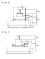
- FIG. 1 schematically shows a cross-sectional view of an SES laser 100 in accordance with a first embodiment of the present invention.
- FIG. 2 schematically shows a plan view of the SES laser 100 shown in FIG. 1.
- the SES laser 100 of the present embodiment includes, as shown in FIG. 1, a light emitting section 140 (referred to as “LE section” hereinafter) and a photodetector section 120 (referred to as “PD section” hereinafter) .
- the LE section 140 generates laser light, which is emitted from an emission surface 108 provided on the PD section 120.
- the PD section 120 has a function to convert a part of laser light generated at the LE section 140 into a (photo-electric) current.
- the LE section 140 and the PD section 120 are described below.
- the LE section 140 is formed on a semiconductor substrate (an n-type GaAs substrate in the present embodiment) 101.
- the LE section 140 forms a vertical resonator (hereinafter referred to as a "resonator").
- the LE section 140 can include a columnar semiconductor deposition body (hereafter referred to as a "columnar portion") 130.
- the LE section 140 is formed from, for example, a distributed reflection type multilayer mirror of 40 pairs of an n-type Al 0.9 Ga 0.1 As layer and an n-type Al 0.15 Ga 0.85 As layer that are alternately laminated (hereafter called a "first mirror") 102, an active layer 103 composed of GaAs well layers and Al 0.3 Ga 0.7 As barrier layers in which the well layers include a quantum well structure composed of three layers, and a distributed reflection type multilayer mirror of 25 pairs (hereafter called a "second mirror") 104, which are successively stacked in layers.
- a distributed reflection type multilayer mirror of 40 pairs of an n-type Al 0.9 Ga 0.1 As layer and an n-type Al 0.15 Ga 0.85 As layer that are alternately laminated hereafter called a "first mirror” 102
- an active layer 103 composed of GaAs well layers and Al 0.3 Ga 0.7 As barrier layers in which the well layers include a quantum well structure composed of three layers
- a distributed reflection type multilayer mirror of 25 pairs here
- a portion among the LE section 140 extending from the second mirror 104 to an intermediate point of the first mirror 102 of the SES laser 100 is etched in a circular shape, as viewed in a direction perpendicular to the emission surface 108, to form a columnar portion 130.
- the columnar portion 130 has a plan configuration that is circular, but can have any arbitrary configuration.
- the second mirror 104 is composed of a first region 104a and a second region 104b. As shown in FIG. 1, the second region 104b is provided above the first region 104a. The second region 104b is in contact with the PD section 120 (more specifically, a first contact layer 111 of the PD section 120).
- the first region 104a has a cross section larger than that of the second region 104b, when cut in planes parallel with a surface 101 a of the semiconductor substrate 101.
- the columnar portion 130 has a step difference formed by the first region 104a and the second region 104b of the second mirror 104.
- the second region 104b is provided in a part of an upper surface 104x of the first region 104a.
- a second electrode 109 (described below) is further provided on the upper surface 104x of the first region 104a.
- the second region 104b has a higher resistance than the first region 104a.
- the second region 104b may be composed of intrinsic semiconductor.
- both of the first region 104a and the second region 104b include an impurity of a first conductivity type (p type), and the concentration of the p-type impurity of the second region 104b is lower than the concentration of the p-type impurity of the first region 104a.
- the first conductivity type is p-type, but the first conductivity type can be n-type. This similarly applies to other embodiments to be described below.
- the impurity concentration of the second region 104b is preferably less than 1 ⁇ 10 16 cm -3 . Furthermore, the second region 104b preferably has a film thickness of 1 ⁇ m or greater.
- the first region 104a is formed from 5 pairs of a p-type Al 0.9 Ga 0.1 As layer and a p-type Al 0.15 Ga 0.85 As layer alternately laminated
- the second region 104b is formed from 20 pairs of a p-type Al 0.9 Ga 0.1 As layer and a p-type Al 0.15 Ga 0.85 As layer alternately laminated.
- the concentration of the p-type impurity of the first region 104a is, for example, 1 ⁇ 10 18 cm -3
- the concentration of the p-type impurity of the second region 104b is, for example, 1 ⁇ 10 15 cm -3 .
- composition of each of the layers and the number of the layers forming the first mirror 102, the active layer 103 and the second mirror 104 are not limited to the above.
- At least the first region 104a among the second mirror 104 is formed to be p-type by, for example, doping C, and the first mirror 102 is formed to be n-type by, for example, doping Si. Accordingly, the first region 104a of the p-type second mirror 104, the undoped active layer 103, and the n-type first mirror 102 form a pin diode.
- a current constricting layer 105 which is composed of aluminum oxide, is formed in a region near the active layer 103 among the first region 104a of the second mirror 104.
- the current constricting layer 105 is formed with a ring-shaped cross section, when cut in a plane parallel with the surface 101 a of the semiconductor substrate 101 shown in FIG. 1.
- the ring-shaped cross-section is defined by two concentric circles.
- the LE section 140 is provided with a first electrode 107 and a second electrode 109.
- the first electrode 107 and the second electrode 109 are used for applying a voltage to the LE section 140 to drive it.
- the second electrode 109 is provided on an upper surface 140a of the LE section 140. More specifically, as shown in FIG. 2, the second electrode 109 has a ring-shaped plane configuration, i.e., a ring shape in plan view.
- the first electrode 107 is provided in a manner to encircle the columnar portion 130
- the second electrode 109 is provided in a manner to encircle the second region 104b of the second mirror 104 and the PD section 120.
- the columnar portion 130 is provided inside the first electrode 107
- the second region 104b of the second mirror 104 and the PD section 120 are provided inside the second electrode 109.
- the first electrode 107 can be formed in any plane configuration.
- the present embodiment is described as having the first electrode 107 provided on the first mirror 102, the first electrode 107 can be formed on the back surface 101 b of the semiconductor substrate 101. This similarly applies to SES lasers in accordance with other embodiments described below.
- the first electrode 107 consists of a multilayer film of an alloy of Au and Ge, and Au.
- the second electrode 109 consists of a multilayer film of Pt, Ti, and Au, for instance.
- An electric current is injected into the active layer 103 by the first electrode 107 and the second electrode 109.
- the material to form the first electrode 107 and the second electrode 109 is not limited to the aforementioned material, and, for instance, an alloy of Au and Zn, etc. can be used.
- the PD section 120 is provided on the LE section 140, and has the emission surface 108.
- the PD section 120 includes a first contact layer 111, a photoabsorption layer 112, and a second contact layer 113.
- the first contact layer 111 is provided on the second mirror 104 of the LE section 140
- the photoabsorption layer 112 is provided on the first contact layer 111
- the second contact layer 113 is provided on the photoabsorption layer 112.
- the plane configuration of the first contact layer 111 is shown to be greater than the plane configuration of the photoabsorption layer 112 or the second contact layer 113 (see FIG. 1 and FIG. 2).
- a third electrode 116 is provided on the first contact layer 111. In other words, the first contact layer 111 is in contact with the third electrode 116.
- the first contact layer 111 can be formed from an n-type GaAs layer.
- the photoabsorption layer 112 can be formed from, for example, an undoped GaAs layer.
- the second contact layer 113 can be formed from a p-type GaAs layer. More specifically, the first contact layer 111 is made n-type by Si doping, for example, and the second contact layer 113 is made p-type by C doping, for example. Therefore, a pin diode is formed by the n-type first contact layer 111, the undoped photoabsorption layer 112, and the p-type second contact layer 113.
- the PD section 120 is provided with the third electrode 116 and a fourth electrode 110.
- the third electrode 116 and the fourth electrode 110 are used for driving the PD section 120.
- the third electrode 116 can be formed from the same material as the first electrode 107
- the fourth electrode 110 can be formed from the same material as the second electrode 109.
- the fourth electrode 110 is provided on an upper surface of the PD section 120 (on the second contact layer 113).
- the fourth electrode 110 is provided with an aperture section 114, and a bottom surface of the aperture section 114 defines the emission surface 108. Accordingly, the shape and the size of the emission surface 108 can be optionally set by appropriately setting the plane configuration and the size of the aperture section 114.
- the present embodiment indicates, as shown in FIG. 1, a case in which the emission surface 108 is circular.
- the n-type first mirror 102 and the p-type second mirror 104 of the LE section 140, and the n-type first contact layer 111 and the p-type second contact layer 113 of the PD section 120 form an npnp structure as a whole.
- the SES laser 100 has three p-n junctions, and the conduction type of the semiconductor changes three times in the structure.
- the p-type and n-type characteristics of each of the semiconductor layers may be interchanged to form a pnpn structure as a whole.
- the conductivity type of the second region 104b of the second mirror 104 is not particularly limited.
- the first conductivity type (p-type) is introduced in the second region 104b.
- the second region 104b can further include impurities of the second conductivity type (n-type).
- the concentration of the first conductivity type impurity and the concentration of the second conductivity type impurity may be made substantially equal to each other in the second region 104b, such that the second region 104b can be made to be semiinsulating.
- the concentration of the first conductivity type impurity can be made greater than the concentration of the second conductivity type impurity in the second region 104b, such that the second region 104b can be of the first conductivity type, or the concentration of the second conductivity type impurity can be made greater than the concentration of the first conductivity type impurity in the second region 104b, such that the second region 104b can be of the second conductivity type.
- the PD section 120 has a function to monitor the output of light generated at the LE section 140. More specifically, the PD section 120 converts light generated at the LE section 140 to an electrical current. The output of light generated by the LE section 140 can be detected by detecting the value of the electrical current.
- a part of light generated at the LE section 140 is absorbed by the photoabsorption layer 112.
- light excitation occurs in the photoabsorption layer 112, and electrons and holes are generated.
- the electrons move to the third electrode 116, and the holes move to the fourth electrode 110.
- a current is generated in a direction from the first contact layer 111 to the second contact layer 113.
- the light output of the LE section 140 is mainly determined by the bias voltage that is applied to the LE section 140.
- the light output of the LE section 140 may substantially change depending of the ambient temperature and the service life of the LE section 140, like a conventional SES laser. For this reason, the light output of the LE section 140 is monitored by the PD section 120.
- a control to feed back the light output of the LE section 140 to control the voltage applied to the LE section 140 can be implemented by using an external electronic circuit (a drive circuit (not shown)).
- the PD section 120 In the PD section 120, light that has entered the first contact layer 111 next enters the photoabsorption layer 112. A part of the entered light is absorbed by the photoabsorption layer 112, such that photoexcitation occurs in the photoabsorption layer 112 whereby electrons and holes are generated. By an electric field applied from outside the device, the electrons move to the third electrode 116, and the holes move to the fourth electrode 110. As a result, in the PD section 120, a current (photoelectric current) is generated in a direction from the first contact layer 111 to the second contact layer 113. By measuring the current values, light outputs of the LE section 140 can be detected. Then, the light that has passed the PD section 120 is emitted from the emission surface 108.
- a current photoelectric current
- FIG. 3 through FIG. 8 are cross-sectional views schematically showing process steps for manufacturing the SES laser 100 shown in FIG. 1, each of which corresponding to the cross-sectional view indicated in FIG. 1.
- a semiconductor multilayer film 150 is formed by epitaxial growth while varying the composition (see FIG. 3).
- the semiconductor multilayer film 150 is formed from, for example, a first mirror 102 of 40 pairs of alternately laminated n-type Al 0.9 Ga 0.1 As layers and n-type Al 0.15 Ga 0.85 As layers, an active layer 103 composed of GaAs well layers and Al 0.3 Ga 0.7 As barrier layers in which the well layers include a quantum well structure composed of three layers, a second mirror 104 composed of a first region 104a and a second region 104b of 5 pairs and 20 pairs of alternately laminated p-type Al 0.9 Ga 0.1 As layers and p-type Al 0.15 Ga 0.85 As layers, respectively, a first contact layer 111 composed of n-type GaAs, a photoabsorption layer 112 composed of GaAs without impurities doped, and a second
- At least one layer adjacent to the active layer 103 is formed as an AlAs layer or an AlGaAs layer having an Al proportion of 0.95 or greater. This layer becomes a current constricting layer 105 when oxidized later (see FIG. 7).
- a second electrode 109 is formed in a later step, at least an area near the portion of the first region 104a of the second mirror 104 which contacts the second electrode 109 is preferably formed to have a high carrier density, such that ohmic contact can be readily made with the second electrode 109.
- At least an area near the portion of the first contact layer 111 which contacts the third electrode 116, and at least an area near the portion of the second contact layer 113 which contacts the fourth electrode 110 are preferably formed to have a high carrier density, such that ohmic contact can be readily made with the third electrode 116 and the fourth electrode 110, respectively.
- the temperature at which the epitaxial growth is conducted is appropriately decided depending on the growth method, the kind of raw material, the type of the semiconductor substrate 101, and the kind, thickness and carrier density of the semiconductor multilayer film 150 to be formed, and in general is preferably 450°C - 800°C.
- the time required when the epitaxial growth is conducted is appropriately decided just as the temperature is decided.
- a metal-organic chemical vapor deposition (MOVPE: Metal-Organic Vapor Phase Epitaxy) method, an MBE method (Molecular Beam Epitaxy) method or an LPE (Liquid Phase Epitaxy) method can be used as a method for the epitaxial growth.
- the second contact layer 113 and the photoabsorption layer 112 are patterned into predetermined configurations (see FIG. 4).
- a photoresist (not shown) is coated on the semiconductor multilayer film 150, and then the photoresist is patterned by a photolithographic method, thereby forming a resist layer R1 having a specified pattern.
- the second contact layer 113 and the photoabsorption layer 112 are etched by, for example, a dry etching method, using the resist layer R1 as a mask.
- the resist layer R1 is removed.
- the first contact layer 111 and the second mirror 104 are patterned into a specified configuration (see FIG. 5). More specifically, first, a photoresist (not shown) is coated on the first contact layer 111 and the second contact layer 113, and then the photoresist is patterned by a photolithographic method, thereby forming a resist layer R2 having a specified pattern (see FIG. 5).
- the first contact layer 111 and the second region 104b of the second mirror 104 are etched by, for example, a dry etching method, using the resist layer R2 as a mask.
- the PD section 120 is formed, as shown in FIG. 5.
- the PD section 120 includes the second contact layer 113, the photoabsorption layer 112 and the first contact layer 111.
- the plane configuration of the first contact layer 111 can be formed to be larger than the plane configuration of the second contact layer 113 and the photoabsorption layer 112. Then, the resist R2 is removed.
- the second contact layer 113 and the photoabsorption layer 112 are patterned, and then the first contact layer 111 is patterned.
- the first contact layer 111 may be patterned, and then the second contact layer 113 and the photoabsorption layer 112 may be patterned to form the PD section 120.
- the LE section 140 including a columnar portion 130 is formed (see FIG. 6). More specifically, first, a photoresist (not shown) is coated on the first region 104a of the second mirror 104 and the PD section 120, and then the photoresist is patterned by a photolithographic method, thereby forming a resist layer R3 having a specified pattern (see FIG. 6).
- the first region 104a of the second mirror 104, the active layer 103, and a part of the first mirror 102 are etched by, for example, a dry etching method, using the resist layer R3 as a mask.
- a columnar portion 130 is formed.
- a resonator (the LE section 140) including the columnar portion 130 is formed on the semiconductor substrate 101.
- a stacked layered body of the PD section 120 and the LE section 140 is formed.
- the resist layer R3 is removed.
- the PD section 120 is formed first, and then the columnar portion 130 is formed.
- the columnar portion 130 may be formed first, and then the PD section 120 may be formed.
- the oxidation rate depends on the temperature of the furnace, the amount of water vapor supply, and the Al proportion and the film thickness of the layer to be oxidized (the layer with the high Al proportion).
- an electric current flows, when it is driven, only in a portion where the current constricting layer is not formed (i.e., a portion that has not been oxidized). Therefore, the current density can be controlled by controlling the range of the current constricting layer 105 to be formed by oxidation.
- the diameter of the current constricting layer 105 is preferably controlled such that a major part of the light emitted from the LE section 140 enters the first contact layer 111.
- a second electrode 109 is formed on an upper surface 104x of the first region 104a of the second mirror 104, and a fourth electrode 110 is formed on an upper surface of the PD section 120 (an upper surface 113a of the second contact layer 113) (see FIG. 8).
- the upper surface 104x of the first region 104a and the upper surface 113a of the second contact layer 113 are washed by using a plasma treatment method, etc. if necessary before the second electrode 109 and the fourth electrode 110 are formed. As a result, a device of more stable characteristics can be formed.
- a multilayer film of Pt, Ti, and Au, for example, (not shown) is formed by, for example, a vacuum deposition method.
- the second electrode 109 and the fourth electrode 110 are formed by removing the multilayer film by a lift-off method at positions other than specified positions. In this case, a portion where the above-mentioned multilayer film is not formed is formed on the upper surface 113a in the second contact layer 113. This portion becomes an opening section 114, and the bottom of the opening section 114 becomes the emission surface 108. It is noted that a dry etching method can be used in the above-mentioned process instead of the lift-off method.
- the second electrode 109 and the fourth electrode 110 are patterned at the same time in the above-mentioned process, the second electrode 109 and the fourth electrode 110 can be individually formed.
- a first electrode 107 is formed on the first mirror 102 of the LE section 140 by patterning a multilayer film of Au and an alloy of Au and Ge, for example, by a similar method, whereby the third electrode 116 is formed on the first contact layer 111 of the PD section 120 (see Fig. 1).
- the temperature of the annealing treatment depends on the electrode material. It is usually conducted at about 400 °C for the electrode material used in the present embodiment.
- the first electrode 107 and the third electrode 116 are formed with the above-described process (see FIG. 1). It is noted here that the first electrode 107 and the third electrode 116 may be patterned and formed at the same time, but the first electrode 107 and the third electrode 116 may be formed individually.
- the SES laser 100 including the LE section 140 and the PD section 120 is obtained by the above-mentioned process (see FIG. 1).
- FIG. 23 is a cross-sectional view schematically showing a conventional SES laser 900.
- the SES laser shown in FIG. 23 includes an LE section 940 and a PD section 920.
- the LE section 940 is formed on a semiconductor substrate 901, and is composed of a multilayer of an n-type first mirror 902, an active layer 903, and a p-type second mirror 904 stacked in layers in this order.
- the PD section 920 is provided on the LE section 940, and is composed of an n-type first contact layer 911, an undoped photoabsorption layer 912, and a p-type second contact layer 913, which are sequentially stacked in layers.
- a first electrode 907 and a second electrode 909 to drive the LE section 940 are provided, and a third electrode 916 and a fourth electrode 910 to drive the PD section 920 are provided.
- a dielectric layer 915 is provided between the LE section 940 and the PD section 120.
- this dielectric layer 915 is formed from a layer including aluminum oxide, and is formed by oxidizing a layer including Al from its side.
- Such an SES laser 900 including a dielectric layer 915 is described in, for example, Japanese Tokuhyo (Japanese Translation of PCT International Application) 2002-504754 and JP-A-2000-183444.
- a voltage is applied between the first electrode 907 and the second electrode 909 to drive the light emitting section 940.
- a prescribed voltage is applied also between the third electrode 916 and the fourth electrode 910 to drive the PD section 920.
- the dielectric layer 915 is obtained by oxidizing a layer (not shown) including Al.
- the layer including Al before it is oxidized is formed "sparsely" so that oxygen may smoothly enter the layer when oxidized and the oxidation may progress easily. Therefore, the dielectric layer 915 obtained by oxidation is "sparse", such that its reliability is low and its mechanical strength is small. Therefore, to secure the reliability and mechanical strength, the film thickness of the dielectric layer 915 needs to be small.
- the second mirror 104 is formed from the first region 104a and the second region 104b, the second region 104b contacts the PD section 120, and the second region 104b has a higher resistance that that of the first region 104a.
- this second region 104b can be formed by an ordinary epitaxial growth method. Consequently, the second region 104b can be formed with a large film thickness. As a result, the parasitic capacitance generated between the LE section 140 and the PD section 120 can be reduced.
- the second region 104b can be formed by an epitaxial growth method just like an ordinary mirror.
- the SES laser 100 of the present embodiment excels the conventional SES laser 900 in reliability and mechanical strength.
- a three terminal structure can be provided.
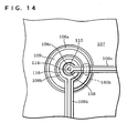
- FIG. 9A - FIG. 9D show ways of connection of the above-described electrodes when the SES laser 100 has a three terminal structure.
- Electrical connection structures that realize the electrode connections indicated in FIG. 9A - FIG. 9D are schematically shown in plan views of FIG. 10 and FIG. 14 - FIG. 16, respectively.
- FIG. 11 - FIG. 13 show cross-sectional views taken along a line A - A, line B - B, and line C - C indicated in the plan view of FIG. 10, respectively.
- FIG. 9A through FIG. 9D indicate electrode connection sections 160a - 160d, respectively.
- the second electrode 109 of the LE section 140 and the third electrode 116 of the PD section 120 are electrically connected at an electrode connection section 160a. More specifically, as shown in FIG. 12 and FIG. 13, the electrode connection section 160a is provided between the SES laser 100 and an electrode pad (not shown), and the second electrode 109 and the third electrode 116 are electrically connected at this electrode connection section 160a. In other words, the second electrode 109 is provided on the third electrode 116 at the electrode connection section 160a.
- the third electrode 116 is formed extending from the first contact layer 111 of the PD section 120 to the dielectric layer 106b.
- the second electrode 109 is formed extending from the first region 104a of the second mirror 104, via the dielectric layer 106b to the dielectric layer 106a and the second electrode 109.
- the dielectric layers 106a, 106b and 106c can be formed together, or may be formed individually. This similarly applies to Connections 2 - 4 described below.
- Connections 2 - 4 although cross-sectional views are omitted, a layer structure similar to that of the SES laser 100 shown in FIG. 10 - FIG. 13 is provided except electrodes to be described below.
- the second electrode 109 of the LE section 140 and the fourth electrode 110 of the PD section 120 are electrically connected at an electrode connection section 160b, as shown in FIG. 14.
- This electrode connection section 160b is provided between the SES laser 100 and an electrode pad (not shown).
- the second electrode 109 is provided on the fourth electrode 110.
- the fourth electrode 110 is formed extending from the second contact layer 113 to the dielectric layer 106c, and the second electrode 109 is formed extending from the first region 104a of the second mirror 104 via the dielectric layer 106c to the fourth electrode 110.
- the first electrode 107 of the LE section 140 and the fourth electrode 110 of the PD section 120 are electrically connected at an electrode connection section 160c, as shown in FIG. 15.
- This electrode connection section 160c is provided between the SES laser 100 and an electrode pad (not shown), in areas excluding the LE section 140 and the PD section 120.
- the first electrode 107 is provided on the fourth electrode 110.
- the fourth electrode 110 is formed extending from the second contact layer 113 to the dielectric layer 106c, and the first electrode 107 is formed extending from the first mirror 102 via the dielectric layer 106c to the fourth electrode 110.
- connection 4 the first electrode 107 of the LE section 140 and the third electrode 116 of the PD section 120 are electrically connected at an electrode connection section 160d, as shown in FIG. 16.
- This electrode connection section 160d is provided between the SES laser 100 and an electrode pad (not shown). At the electrode connection section 160d, the first electrode 107 is provided on the third electrode 116.
- the third electrode 116 is formed extending from the first contact layer 111 to the dielectric layer 106b, and the first electrode 107 is formed extending from the first mirror 102 via the dielectric layer 106d to the third electrode 116.
- connection 1 the second electrode 109 of the LE section 140 and the third electrode 116 of the PD section 120 are electrically connected, as shown in FIG. 9A.
- a parasitic capacitance is not created between the LE section 140 and the PD section 120 because no potential difference occurs between the second electrode 109 and the third electrode 116.
- the second electrode 109 of the LE section 140 and the fourth electrode 110 of the PD section 120 are electrically connected, as shown in FIG. 9B.
- a potential difference is generated between the second electrode 109 and the fourth electrode 110, and as a result, a parasitic capacitance C p is created.
- the parasitic capacitance C p is large. In other words, the smaller the film thickness of the "layer of a high nonconductivity", the greater the parasitic capacitance C p .
- a parasitic capacitance C p is similarly created in Connections 3 and 4, when a potential difference is generated between the first electrode 107 and the fourth electrode 110 and between the first electrode 107 and the third electrode 116.
- a dielectric layer 915 is provided between the LE section 940 and the PD section 120.
- the dielectric layer 915 that is formed by oxidizing a layer including Al has a small mechanical strength.
- the mechanical strength of the SES laser 100 decreases when the film of the dielectric layer 915 is formed to thick. Therefore, the dielectric layer 915 needs to be formed thinly to some degree.
- the parasitic capacitance C p between the light emitting element 940 and the PD section 120 becomes larger.
- the second region 104b in the second mirror 104 of the LE section 140 has a higher resistance than the first region 104a, and the second region 104b contacts the PD section 120. Therefore, this second region 104b corresponds to a "layer having a high nonconductivity" provided between the LE section 140 and the PD section 120 in the above-described Connections 2 - 4.
- the second region 104b is a part of the second mirror 104, the second region 104b can be formed by an ordinary epitaxial growth method. Therefore, the second region 104b can be formed with a great film thickness.
- the second region 104b that is a "layer having a high nonconductivity" provided between the LE section 140 and the PD section 120 can be formed with a great film thickness.
- the parasitic capacitance C p can be controlled in the above described Connections 2 - 4, the SES laser 100 can be driven at a high-speed.
- any of Connections 1 - 4 can be applied to the SES laser 100 according to the present embodiment.
- the SES laser 100 with a three terminal structure that has a degree of freedom in choosing structures and can be driven at high-speed can be obtained.
- the SES laser 100 with a three terminal structure in different inter-electrode connections can be obtained without changing the manufacturing processes other than the electrode forming process.
- the second mirror 104 is provided on the active layer 103, and the second region 104b is provided on the first region 104a in the second mirror 104.
- the first electrode 107 and the second electrode 109 to drive the LE section 140 are included, and the second electrode 109 contacts the first region 104a of the second mirror 104.
- the second electrode 109 is provided in a much closer proximity to the active layer 103, the voltage can be efficiently applied to the active layer 103.
- the second region 104b is provided on the first region 104a
- the second electrode 109 is provided on the first region 104a, such that an electric current does not flow to the second region 104b.
- carriers do not move in the second region 104b, and carriers move only in the first region 104a. Therefore, because carriers can move in the SES laser 100 via a heterojunction with fewer carriers, the SES laser 100 with a lower resistance can be obtained.
- the second region 104b of the second mirror 104 compared to the first region 104a, has a concentration of impurities of the same conductivity type as that of the first region 104a which is lower than that of the first region 104a, or impurities of the same conductivity type are not added. Consequently, the second region 104b has a higher resistance than that of the first region 104a.
- FIG. 17 schematically shows a cross-sectional view of an SES laser 200 in accordance with a second embodiment of the present invention.
- FIG. 18 schematically shows a plan view of the SES laser 200 shown in FIG. 17.
- the SES laser 200 of the present embodiment has a structure different from the SES laser 100 of the first embodiment in that a reflection layer 305 is provided in the second region 104b of the second mirror 104.
- the SES laser 200 is similar in its structure to the SES laser 100 of the first embodiment except for this point. Accordingly, the same reference signs are assigned to components similar to those of the SES laser 100 of the first embodiment and their detailed description is omitted.
- the reflection layer 305 has the function to reflect spontaneous emission light.
- the reflection layer 305 can be formed by using the same material (a layer including aluminum oxide) as that of the current constricting layer 105 for instance. In this case, the reflection layer 305 can be formed by a process similar to that used for the current constricting layer 105. More specifically, a layer (not shown) having a high Al proportion is formed in the second region 104b of the second mirror 104 in advance, and the reflection layer 305 can be formed by oxidizing this layer from its side.
- An aluminum oxide (AIOx) layer is usually a dielectric layer whose refractive index is lower than that of a surrounding semiconductor layer.
- the refractive index of an aluminum oxide layer is about 1.6, and the refractive index of a semiconductor layer is usually 2.9 - 3.5.
- the film thickness of the reflection layer 305 can be set to n/4 (n is a natural number) of the wavelength of the laser light generated at the LE section 140. As a result, the reflection of modes of the above-described laser light can be increased.
- the operations of the SES laser 200 of the present embodiment are similar in principle to those of the SES laser 100 of the first embodiment, and therefore their detailed description is omitted.
- the SES laser 200 in accordance with the second embodiment substantially has the same actions and effects as the SES laser 100 in accordance with the first embodiment.
- the PD section 120 has a function to detect the light output of the LE section 140. Therefore, the output of light generated at the LE section 140 might not be detected correctly, if light other than the laser light generated at the light emitting element 140 enters the PD section 120.
- the reflection layer 305 is provided in the second region 104b of the second mirror 104, such that spontaneous emission light is prevented from entering the PD section 120. As a result, only the laser light generated in the LE section 140 can be injected in the PD section 120, such that the output of light generated in the LE section 140 can be detected more accurately by the PD section 120.
- the efficiency of the PD section might decrease by this reflection layer.
- the reflection layer 305 is provided in the second region 104b of the second mirror 104 but not in the PD section 120, such that the efficiency of the PD section 120 is not lowered by the existence of the reflection layer 305.
- the reflection layer 305 can be set up regardless of the current path because the reflection layer 305 is provided in the second region 104b of the second mirror 104. In other words, the current path is not affected by setting up the reflection layer 305. Therefore, the characteristics of the LE section 140 are not changed as a result of the provision of the reflection layer 305.
- the reflection layer 305 does not need a new manufacturing process because it can be formed by applying the design of mirrors ordinarily used.
- FIG. 19 schematically shows a cross-sectional view of a SES laser 300 in accordance with a third embodiment of the present invention.
- the SES laser 300 of the present embodiment has a structure different from the SES laser 100 of the first embodiment in that a PD section 220 and an LE section 240 are stacked in layers in this order on a semiconductor substrate 201.
- components of the SES laser 300 which are similar to components of the SES laser 100 of the first embodiment, are denoted by reference signs increased by 100 as compared to those used in the context of SES laser 100.
- reference signs "2 ⁇ ” represent components similar to the components "1 ⁇ ” of the SES laser 100 of the first embodiment, and are principally composed of similar materials, their detailed description is omitted.
- the SES laser 300 of the present embodiment includes a PD section 220 provided on a semiconductor substrate 201, and an LE section 240 provided on the PD section 220.
- the SES laser 300 emits light generated in the LE section 240 from its emission surface 208.
- the PD section 220 includes a second contact layer 213, a photoabsorption layer 212, and a first contact layer 211.
- the second contact layer 213 of p-type, the photoabsorption layer 212, and the first contact layer 211 of n-type are stacked in layers in this order on the semiconductor substrate 201 of p-type GaAs.
- the second contact layer 213, the photoabsorption layer 212, and the first contact layer 211 can be formed from the same material as the second contact layer 113, the photoabsorption layer 112 and the first contact layer 111 of the first embodiment, respectively.
- the LE section 240 includes a second mirror 204, an active layer 203, and a first mirror 202.
- the second mirror 204 consists of a first region 204a and a second region 204b.
- the second region 204b contacts the PD section 220, and has a higher resistance than the first region 204a.
- the first region 204a and second region 204b of p-type of the second mirror 204, the active layer 203, and the first mirror 202 of n-type are stacked in layers in this order on the PD section 220.
- the first region 204a and second region 204b of the second mirror 204, the active layer 203, and the first mirror 202 can be formed from the same material as the first region 104a and second region 104b of the second mirror 104, the active layer 103, and the first mirror 102 of the first embodiment, respectively.
- a current constricting layer 205 is provided in the second mirror 204, like the second mirror 104 in the first embodiment.
- the SES laser 300 of the present embodiment also includes a first electrode 207, a second electrode 209, a third electrode 216 and a fourth electrode 210.
- the first electrode 207 and the second electrode 209 are used to drive the LE section 240.
- the third electrode 216 and the fourth electrode 210 are used to drive the PD section 220.
- the first electrode 207 is provided on the first mirror 202.
- the second electrode 209 contacts the first region 204a of the second mirror 204.
- the third electrode 216 is provided on the first contact layer 211.
- the fourth electrode 210 is provided on the second contact layer 213.
- the second electrode 209, the third electrode 216 and the fourth electrode 210 can have a ring-shaped planar configuration.
- the second electrode 209 is provided to surround the LE section 240
- the third electrode 216 is provided to surround the LE section 240 and the first region 204a of the second mirror 204
- the fourth electrode 210 is provided to surround the first contact layer 211 and the photoabsorption layer 212.
- the emission surface 208 is provided on the upper surface (surface 201 a) of the SES laser 300. More specifically, in the SES laser 300, an opening 214, that penetrates the semiconductor substrate 201, is provided in the semiconductor substrate 201, and the bottom of this opening 214 defines the emission surface 208.
- the order of stacked layers of the LE section 240 and the PD section 220 on the semiconductor substrate 201 is reverse to the of the SES laser 100 of the first embodiment.
- basic operations of the SES laser 300 of the present embodiment are similar to those of the SES laser 100 of the first embodiment, a detailed description thereof is omitted.
- the laser light passes the PD section 220 and goes out from the emission surface 208. It is noted here that a part of the laser light generated in the light emitting element 240 is absorbed by the photoabsorption layer 212 of the PD section 220, and converted into an electric current, thereby detecting an output of the light generated by the LE section 240.
- the SES laser 300 in accordance with the present embodiment substantially has the same actions and effects as the SES laser 100 in accordance with the first embodiment.
- FIG. 20 is a view schematically showing an optical module 500 in accordance with a fourth embodiment of the present invention.
- the optical module 500 includes the SES laser 100 of the first embodiment (see FIG. 1), a semiconductor chip 20 and an optical fiber 30. It is noted that, in the optical module 500 of the present embodiment, the same actions and effects can be obtained even when the SES laser of the second or the third embodiment is used instead of the SES laser 100 of the first embodiment. The same applies to fifth and sixth embodiments to be described below.
- the SES laser 100 absorbs light that is emitted from an end face 30a of the optical fiber 30.
- the SES laser 100 is in a state in which its position relative to the end face 30a of the optical fiber 30 is fixed. More specifically, the emission surface 108 of the SES laser 100 opposes the end face 30a of the optical fiber 30.
- the semiconductor chip 20 is provided for driving the SES laser 100.
- the semiconductor chip 20 is provided with a built-in circuit for driving the SES laser 100.
- the semiconductor chip 20 includes a plurality of electrodes (or pads) 22 formed therein that are electrically connected to the internal circuit. Wiring patterns 24 and 64, which are electrically connected to at least one of the electrodes 22, are preferably formed on a surface where the electrodes 22 are formed.
- the semiconductor chip 20 and the SES laser 100 are electrically connected with each other.
- a wiring pattern 14 and the wiring pattern 24 formed on the semiconductor chip 20 are electrically connected with one another through solder 26.
- the wiring pattern 14 is electrically connected to the first electrode 107 of the SES laser 100 (not shown in FIG. 20).
- the wiring pattern 34 is electrically connected to the wiring pattern 64 formed on the semiconductor chip 20 through solder 26.
- the wiring pattern 34 is electrically connected to the first electrode 107 of the SES laser 100 (not shown in FIG. 20).
- the third electrode 116 and the fourth electrode 110 of the SES laser 100 are electrically connected to wiring patterns (not shown).
- the SES laser 100 can be face-down mounted on the semiconductor chip 20.
- the solder 26 not only provides electrical connection, but also fixes the SES laser 100 and the semiconductor chip 20. It is noted that, for connection between the wiring patterns 14 and the wiring patterns 24, and between the wiring patterns 34 and the wiring patterns 64, wires or conductive paste may be used.
- An underfill material 40 may be provided between the SES laser 100 and the semiconductor chip 20.
- the underfill material 40 covers the emission surface 108 of the SES laser 100
- the underfill material 40 is preferably transparent.
- the underfill material 40 covers and protects electrical connection sections between the SES laser 100 and the semiconductor chip 20, and also protects the surfaces of the SES laser 100 and the semiconductor chip 20. Furthermore, the underfill material 40 maintains the connected state between the SES laser 100 and the semiconductor chip 20.
- An aperture 28 may be formed in the semiconductor chip 20.
- the optical fiber 30 is inserted in the aperture 28.
- the aperture 28 is formed extending from the surface where the electrodes 22 are formed to the opposite surface, while avoiding the internal circuit.
- a taper 29 is preferably formed at an edge section of at least one of openings of the aperture 28. By forming the taper 29, the optical fiber 30 can be more easily inserted in the aperture 28.
- the semiconductor chip 20 may be attached to a substrate 42. More specifically, the semiconductor chip 20 may be attached to the substrate 42 through adhesive 44.
- An aperture 46 is formed in the substrate 42.
- the aperture 46 is formed at a position that connects to the aperture 28 of the semiconductor chip 20.
- the adhesive 44 that adheres the semiconductor chip 20 to the substrate 42 is provided in a manner not to disturb the continuation of the two apertures 28 and 46 and not to block them.
- the aperture 46 in the substrate 42 has a tapered configuration such that its inner diameter becomes greater in a direction opposite to the semiconductor chip 20. By this, the optical fiber 30 can be readily inserted.
- the substrate 42 may be formed from a material that is nonconductive, such as resin, glass, ceramics or the like, but may be formed from a material that is conductive, such as metal or the like.
- a dielectric film 43 is preferably formed at least on the surface on which the semiconductor chip 20 is mounted. It is noted that a material similar to that of the substrate 42 can also be used in embodiments to be described below.
- the substrate 42 preferably has a high thermal conductivity.
- the substrate 42 promotes dissipation/radiation of heat of at least one of the semiconductor device 100 and the semiconductor chip 20.
- the substrate 42 functions as a heat sink or a heat spreader.
- the substrate 42 is adhered to the semiconductor chip 20, and therefore can directly cool the semiconductor chip 20.
- the adhesive 44 that adheres the semiconductor chip 20 to the substrate 42 preferably has a thermal conductivity.
- the SES laser 100 connected to the semiconductor chip 20 is also cooled.
- the substrate 42 is provided with wiring patterns 48.
- the substrate 42 is provided with external terminals 50. In the present embodiment, the external terminals 50 are leads.
- the wiring patterns 48 that are formed on the substrate 42 are electrically connected, for example, through wires 52, to the electrodes 22 of the semiconductor chip 20 and at least one of the wiring patterns 24 and 64 formed on the semiconductor chip 20.
- the wiring patterns 48 may be electrically connected to the external terminals 50.
- the optical fiber 30 is inserted in the aperture 28 of the semiconductor chip 20.
- the optical fiber 30 is passed through the aperture 46 of the substrate 42.
- the inner diameter of the aperture 46 gradually reduces toward the aperture 28 of the semiconductor chip 20, and the inner diameter of the aperture 46 is greater than that of the optical fiber 30 on the surface opposite to the semiconductor chip 20.
- a gap between the optical fiber 30 and the inner surface of the aperture 46 is preferably filled with a filler material 54 such as resin.
- the filler material 54 also has a function to fix and prevent the optical fiber 30 from slipping out.
- the optical fiber 30 may be a single mode fiber, or a multiple mode fiber.
- a multiple mode fiber may be used as the optical fiber 30, such that light emitted from the SES laser 100 can be securely introduced into the optical fiber 30.
- the SES laser 100 and the semiconductor chip 20 are sealed with resin 56.
- the resin 56 also seals electrically connected sections between the SES laser 100 and the semiconductor chip 20 and electrically connected sections between the semiconductor chip 20 and the wiring patterns 48 formed on the substrate 42.
- FIG. 21 is a diagram showing optical transmission devices in accordance with a fifth embodiment of the present invention.
- the optical transmission devices 90 connect electronic devices 92, such as a computer, display device, storage device, printer and the like, with each other.
- the electronic devices 92 may be information communication devices.
- the optical transmission device 90 may include a cable 94 and plugs 96 provided on both sides of the cable 94.
- the cable 94 includes an optical fiber 30 (see FIG. 20).
- the plug 96 includes an SES laser 100 and a semiconductor chip 20. It is noted that the optical fiber 30 is provided inside the cable 94, and the SES laser 100 and the semiconductor chip 20 are provided inside the plug 96, and therefore they are not shown in FIG. 21.
- the optical fiber 30 and the SES laser 100 are attached in a manner described in the fourth embodiment.
- the SES laser 100 of the first embodiment is provided at one end of the optical fiber 30, and a photodetector (not shown) is provided at the other end of the optical fiber 30.
- the photodetector converts inputted optical signals into electrical signals, and then provides the electrical signals to an electronic device 92 on one side.
- electrical signals outputted from the electronic device 92 are converted by the SES laser 100 into optical signals.
- the optical signals are transmitted through the optical fiber 30 and inputted in the photodetector.
- information can be transmitted among the electronic devices 92 by optical signals.
- FIG. 22 is a diagram showing a usage configuration of optical transmission devices in accordance with a sixth embodiment of the present invention.
- Optical transmission devices 90 connect electronic devices 80.
- the electronic devices 80 include liquid crystal display monitors, digital CRTs (which may be used in the fields of finance, mail order, medical treatment, and education), liquid crystal projectors, plasma display panels (PDP), digital TVs, cash registers of retail stores (for POS (Point of Sale) scanning), videos, tuners, gaming devices, printers and the like.
- the present invention is not limited to the embodiments described above, and many modifications can be made.
- an LE section having one columnar portion is described.
- a plurality of columnar portions may be provided in the LE section. Similar functions and effects are obtained even when a plurality of SES lasers are provided in an array.
- each of the semiconductor layers in the above described embodiments may be substituted for one another.
- the description is made as to an AlGaAs type, but depending on the oscillation wavelength to be generated, other materials, such as, for example, GaInP type, ZnSSe type, InGaN type, AlGaN type, InGaAs type, GaInNAs type, GaAsSb type, and like semiconductor materials can be used.
- an SES laser of the present invention is formed by using a semiconductor material such as GaAsSb type, InGaAs type, and GaInN As type, and when laser light of a long wavelength is generated in the active layer, the Auger non-radiative recombination in the second region of the second mirror can be decreased by reducing the concentration of impurities included in the second region of the second mirror lower than the first region. As a result, the luminous efficiency of the SES laser can be greatly improved.
Abstract
Description
- The present invention relates to a surface-emitting type semiconductor laser, an optical module and an optical transmission device.
- With a surface-emitting type semiconductor laser (simply referred to as "SES laser" hereinafter) the light output varies depending on the ambient temperature. For this reason, in some cases, an optical module that uses an SES laser may be equipped with a photodetector function that detects a part of the laser light emitted from the SES laser to thereby monitor the light output. For example, a photodetector section such as a photodiode or the like may be provided in an SES laser, such that a part of laser light emitted from the SES laser can be monitored within the same device (JP-A-10-135568). However, when a photodetector section is provided within an SES laser, the degree of freedom in selecting structures may be lowered because the structure of the SES laser is limited, in view of polarity of each of the layers that compose a section that contributes to generation of laser light (i.e., a light emitting section) and the photodetector section, and the structure of the light emitting section and the photodetector section.
- SES lasers can be driven at high speeds, and by taking advantage of this characteristics, they are adopted in electronic devices and optical communication systems. Accordingly, operations at high speeds are also demanded for an SES laser equipped with a photodetector section.
- It is an object of the present invention to provide an SES laser including a photodetector section, which has a high degree of freedom in selecting structures, and is capable of high-speed driving. It is another object of the present invention to provide an optical module and an optical transmission device, which includes the SES laser.
- These objects are achieved by a surface-emitting type semiconductor (SES) laser as claimed in
claim 1. Preferred embodiments and uses of the invention are subject-matter of the dependent claims. - The SES laser in accordance with the present invention, where the second region has a higher resistance than the first region, has a high degree of freedom in selecting structure, and is capable of high-speed driving. Details thereof will be described in embodiments of the present invention.
- Preferred embodiments of the present invention will be described below with reference to the accompanying drawings, in which:
- FIG. 1
- schematically shows a cross-sectional view of an SES laser in accordance with a first embodiment of the present invention;
- FIG. 2
- schematically shows a plan view of the SES laser shown in FIG. 1;
- FIGs. 3
- to 8 are a cross-sectional views schematically showing steps of manufacturing the SES laser shown in FIG. 1;
- FIG. 9A - FIG. 9D
- schematically show connection methods for electrodes of the SES laser shown in FIG. 1;
- FIG. 10
- is a plan view schematically showing an electrode structure of the SES laser shown in FIG. 1, when the connection method indicated in FIG. 9A is used;
- FIG. 11
- schematically shows a cross-sectional views taken along a line A - A of the SES laser shown in FIG. 10;
- FIG. 12
- schematically shows a cross-sectional views taken along a line B - B of the SES laser shown in FIG. 10;
- FIG. 13
- schematically shows a cross-sectional views taken along a line C - C of the SES laser shown in FIG. 10;
- FIG. 14
- is a plan view schematically showing an electrode structure of the SES laser shown in FIG. 1, when the connection method indicated in FIG. 9B is used;
- FIG. 15
- is a plan view schematically showing an electrode structure of the SES laser shown in FIG. 1, when the connection method indicated in FIG. 9C is used;
- FIG. 16
- is a plan view schematically showing an electrode structure of the SES laser shown in FIG. 1, when the connection method indicated in FIG. 9D is used;
- FIG. 17
- schematically shows a cross-sectional view of an SES laser in accordance with a second embodiment of the present invention;
- FIG. 18
- schematically shows a plan view of the SES laser shown in FIG. 17;
- FIG. 19
- schematically shows a cross-sectional view of an SES laser in accordance with a third embodiment of the present invention;
- FIG. 20
- is a view schematically showing an optical module in accordance with a fourth embodiment of the present invention;
- FIG. 21
- is a view showing optical transmission devices in accordance with a fifth embodiment of the present invention;
- FIG. 22
- is a view showing a usage configuration of optical transmission devices in accordance with a sixth embodiment of the present invention;
- FIG. 23
- schematically shows a cross-sectional view of one example of a conventional SES laser.
- FIG. 1 schematically shows a cross-sectional view of an
SES laser 100 in accordance with a first embodiment of the present invention. FIG. 2 schematically shows a plan view of theSES laser 100 shown in FIG. 1. - The
SES laser 100 of the present embodiment includes, as shown in FIG. 1, a light emitting section 140 (referred to as "LE section" hereinafter) and a photodetector section 120 (referred to as "PD section" hereinafter) . In thisSES laser 100, theLE section 140 generates laser light, which is emitted from anemission surface 108 provided on thePD section 120. ThePD section 120 has a function to convert a part of laser light generated at theLE section 140 into a (photo-electric) current. TheLE section 140 and thePD section 120 are described below. - Light Emitting (LE) Section
- The
LE section 140 is formed on a semiconductor substrate (an n-type GaAs substrate in the present embodiment) 101. TheLE section 140 forms a vertical resonator (hereinafter referred to as a "resonator"). TheLE section 140 can include a columnar semiconductor deposition body (hereafter referred to as a "columnar portion") 130. - The
LE section 140 is formed from, for example, a distributed reflection type multilayer mirror of 40 pairs of an n-type Al0.9Ga0.1As layer and an n-type Al0.15 Ga0.85As layer that are alternately laminated (hereafter called a "first mirror") 102, anactive layer 103 composed of GaAs well layers and Al0.3Ga0.7As barrier layers in which the well layers include a quantum well structure composed of three layers, and a distributed reflection type multilayer mirror of 25 pairs (hereafter called a "second mirror") 104, which are successively stacked in layers. - A portion among the
LE section 140 extending from thesecond mirror 104 to an intermediate point of thefirst mirror 102 of theSES laser 100 is etched in a circular shape, as viewed in a direction perpendicular to theemission surface 108, to form acolumnar portion 130. It is noted that, in the present embodiment, thecolumnar portion 130 has a plan configuration that is circular, but can have any arbitrary configuration. - The
second mirror 104 is composed of afirst region 104a and asecond region 104b. As shown in FIG. 1, thesecond region 104b is provided above thefirst region 104a. Thesecond region 104b is in contact with the PD section 120 (more specifically, afirst contact layer 111 of the PD section 120). In theSES laser 100, as shown in FIG. 1 and FIG. 2, thefirst region 104a has a cross section larger than that of thesecond region 104b, when cut in planes parallel with asurface 101 a of thesemiconductor substrate 101. As a result, thecolumnar portion 130 has a step difference formed by thefirst region 104a and thesecond region 104b of thesecond mirror 104. In other words, thesecond region 104b is provided in a part of anupper surface 104x of thefirst region 104a. A second electrode 109 (described below) is further provided on theupper surface 104x of thefirst region 104a. - The
second region 104b has a higher resistance than thefirst region 104a. For example, thesecond region 104b may be composed of intrinsic semiconductor. In theSES laser 100 of the present embodiment, both of thefirst region 104a and thesecond region 104b include an impurity of a first conductivity type (p type), and the concentration of the p-type impurity of thesecond region 104b is lower than the concentration of the p-type impurity of thefirst region 104a. It is noted that, in the present embodiment, the first conductivity type is p-type, but the first conductivity type can be n-type. This similarly applies to other embodiments to be described below. - The impurity concentration of the
second region 104b is preferably less than 1×1016 cm-3. Furthermore, thesecond region 104b preferably has a film thickness of 1 µm or greater. - More specifically, the
first region 104a is formed from 5 pairs of a p-type Al0.9Ga0.1As layer and a p-type Al0.15Ga0.85As layer alternately laminated, thesecond region 104b is formed from 20 pairs of a p-type Al0.9Ga0.1As layer and a p-type Al0.15Ga0.85As layer alternately laminated. In this case, the concentration of the p-type impurity of thefirst region 104a is, for example, 1×1018 cm-3, and the concentration of the p-type impurity of thesecond region 104b is, for example, 1×1015 cm-3. - It is noted that the composition of each of the layers and the number of the layers forming the
first mirror 102, theactive layer 103 and thesecond mirror 104 are not limited to the above. - At least the
first region 104a among thesecond mirror 104 is formed to be p-type by, for example, doping C, and thefirst mirror 102 is formed to be n-type by, for example, doping Si. Accordingly, thefirst region 104a of the p-typesecond mirror 104, the undopedactive layer 103, and the n-typefirst mirror 102 form a pin diode. - A
current constricting layer 105, which is composed of aluminum oxide, is formed in a region near theactive layer 103 among thefirst region 104a of thesecond mirror 104. Thecurrent constricting layer 105 is formed with a ring-shaped cross section, when cut in a plane parallel with thesurface 101 a of thesemiconductor substrate 101 shown in FIG. 1. The ring-shaped cross-section is defined by two concentric circles. - The
LE section 140 is provided with afirst electrode 107 and asecond electrode 109. Thefirst electrode 107 and thesecond electrode 109 are used for applying a voltage to theLE section 140 to drive it. Thesecond electrode 109 is provided on an upper surface 140a of theLE section 140. More specifically, as shown in FIG. 2, thesecond electrode 109 has a ring-shaped plane configuration, i.e., a ring shape in plan view. Thefirst electrode 107 is provided in a manner to encircle thecolumnar portion 130, and thesecond electrode 109 is provided in a manner to encircle thesecond region 104b of thesecond mirror 104 and thePD section 120. In other words, thecolumnar portion 130 is provided inside thefirst electrode 107, and thesecond region 104b of thesecond mirror 104 and thePD section 120 are provided inside thesecond electrode 109. It is noted that thefirst electrode 107 can be formed in any plane configuration. - Although the present embodiment is described as having the
first electrode 107 provided on thefirst mirror 102, thefirst electrode 107 can be formed on theback surface 101 b of thesemiconductor substrate 101. This similarly applies to SES lasers in accordance with other embodiments described below. - For instance, the
first electrode 107 consists of a multilayer film of an alloy of Au and Ge, and Au. Thesecond electrode 109 consists of a multilayer film of Pt, Ti, and Au, for instance. An electric current is injected into theactive layer 103 by thefirst electrode 107 and thesecond electrode 109. The material to form thefirst electrode 107 and thesecond electrode 109 is not limited to the aforementioned material, and, for instance, an alloy of Au and Zn, etc. can be used. - Photodetector (PD) Section
- The
PD section 120 is provided on theLE section 140, and has theemission surface 108. ThePD section 120 includes afirst contact layer 111, aphotoabsorption layer 112, and asecond contact layer 113. Thefirst contact layer 111 is provided on thesecond mirror 104 of theLE section 140, thephotoabsorption layer 112 is provided on thefirst contact layer 111, and thesecond contact layer 113 is provided on thephotoabsorption layer 112. Furthermore, in the case of thePD section 120 of the present embodiment, the plane configuration of thefirst contact layer 111 is shown to be greater than the plane configuration of thephotoabsorption layer 112 or the second contact layer 113 (see FIG. 1 and FIG. 2). Athird electrode 116 is provided on thefirst contact layer 111. In other words, thefirst contact layer 111 is in contact with thethird electrode 116. - For example, the
first contact layer 111 can be formed from an n-type GaAs layer. Thephotoabsorption layer 112 can be formed from, for example, an undoped GaAs layer. Thesecond contact layer 113 can be formed from a p-type GaAs layer. More specifically, thefirst contact layer 111 is made n-type by Si doping, for example, and thesecond contact layer 113 is made p-type by C doping, for example. Therefore, a pin diode is formed by the n-typefirst contact layer 111, theundoped photoabsorption layer 112, and the p-typesecond contact layer 113. - The
PD section 120 is provided with thethird electrode 116 and afourth electrode 110. Thethird electrode 116 and thefourth electrode 110 are used for driving thePD section 120. In theSES laser 100 of the present embodiment, thethird electrode 116 can be formed from the same material as thefirst electrode 107, and thefourth electrode 110 can be formed from the same material as thesecond electrode 109. - The
fourth electrode 110 is provided on an upper surface of the PD section 120 (on the second contact layer 113). Thefourth electrode 110 is provided with anaperture section 114, and a bottom surface of theaperture section 114 defines theemission surface 108. Accordingly, the shape and the size of theemission surface 108 can be optionally set by appropriately setting the plane configuration and the size of theaperture section 114. The present embodiment indicates, as shown in FIG. 1, a case in which theemission surface 108 is circular. - Overall Configuration
- In the
SES laser 100 of the present first embodiment, the n-typefirst mirror 102 and the p-typesecond mirror 104 of theLE section 140, and the n-typefirst contact layer 111 and the p-typesecond contact layer 113 of thePD section 120 form an npnp structure as a whole. In other words, theSES laser 100 has three p-n junctions, and the conduction type of the semiconductor changes three times in the structure. It should be noted that, for example, the p-type and n-type characteristics of each of the semiconductor layers may be interchanged to form a pnpn structure as a whole. These features can be similarly applied to SES lasers in accordance with other embodiments to be described below. - The conductivity type of the
second region 104b of thesecond mirror 104 is not particularly limited. In theSES laser 100 of the present embodiment, the first conductivity type (p-type) is introduced in thesecond region 104b. Thesecond region 104b can further include impurities of the second conductivity type (n-type). In this case, the concentration of the first conductivity type impurity and the concentration of the second conductivity type impurity may be made substantially equal to each other in thesecond region 104b, such that thesecond region 104b can be made to be semiinsulating. The concentration of the first conductivity type impurity can be made greater than the concentration of the second conductivity type impurity in thesecond region 104b, such that thesecond region 104b can be of the first conductivity type, or the concentration of the second conductivity type impurity can be made greater than the concentration of the first conductivity type impurity in thesecond region 104b, such that thesecond region 104b can be of the second conductivity type. - The
PD section 120 has a function to monitor the output of light generated at theLE section 140. More specifically, thePD section 120 converts light generated at theLE section 140 to an electrical current. The output of light generated by theLE section 140 can be detected by detecting the value of the electrical current. - More specifically, in the
PD section 120, a part of light generated at theLE section 140 is absorbed by thephotoabsorption layer 112. By the absorbed light, light excitation occurs in thephotoabsorption layer 112, and electrons and holes are generated. By an electric field applied from outside the device, the electrons move to thethird electrode 116, and the holes move to thefourth electrode 110. As a result, in thePD section 120, a current is generated in a direction from thefirst contact layer 111 to thesecond contact layer 113. - The light output of the
LE section 140 is mainly determined by the bias voltage that is applied to theLE section 140. In theSES laser 100, the light output of theLE section 140 may substantially change depending of the ambient temperature and the service life of theLE section 140, like a conventional SES laser. For this reason, the light output of theLE section 140 is monitored by thePD section 120. In other words, by adjusting the voltage applied to theLE section 140 depending on the value of the current generated at thePD section 120, to thereby adjust the current flowing in theLE section 140, a predetermined light output level can be maintained at theLE section 140. A control to feed back the light output of theLE section 140 to control the voltage applied to theLE section 140 can be implemented by using an external electronic circuit (a drive circuit (not shown)). - General operations of the
SES laser 100 of the present embodiment are described below. It is noted that the following method for operating theSES laser 100 is described as an example only. - When applying a voltage in a forward direction to the pin diode between the
first electrode 107 and thesecond electrode 109, recombinations of electrons and holes occur in theactive layer 103 of theLE section 140, thereby causing emission of light due to the recombinations. Stimulated emission occurs during the period the generated light reciprocates between thesecond mirror 104 and thefirst mirror 102, whereby the light intensity is amplified. When the optical gain exceeds the optical loss, laser oscillation occurs, whereby laser light is generated at theactive layer 103. The laser light is emitted from thesecond mirror 104 of theLE section 140, and enters thefirst contact layer 111 of thePD section 120. - In the
PD section 120, light that has entered thefirst contact layer 111 next enters thephotoabsorption layer 112. A part of the entered light is absorbed by thephotoabsorption layer 112, such that photoexcitation occurs in thephotoabsorption layer 112 whereby electrons and holes are generated. By an electric field applied from outside the device, the electrons move to thethird electrode 116, and the holes move to thefourth electrode 110. As a result, in thePD section 120, a current (photoelectric current) is generated in a direction from thefirst contact layer 111 to thesecond contact layer 113. By measuring the current values, light outputs of theLE section 140 can be detected. Then, the light that has passed thePD section 120 is emitted from theemission surface 108. - With the
SES laser 100 of the present embodiment, a part of light output of theLE section 140 is monitored by thePD section 120 and the result is fed back to the drive circuit, whereby variations in the output due to temperature changes or the like can be corrected, and therefore stable light output can be obtained. - Next, one example of the method for manufacturing the
SES laser 100 in accordance with the first embodiment of the present invention will be described with reference to FIG. 3 through FIG. 8. FIG. 3 through FIG. 8 are cross-sectional views schematically showing process steps for manufacturing theSES laser 100 shown in FIG. 1, each of which corresponding to the cross-sectional view indicated in FIG. 1. - (1) First, as shown in FIG. 3, on the
surface 101 a of thesemiconductor substrate 101 formed of n-type GaAs, asemiconductor multilayer film 150 is formed by epitaxial growth while varying the composition (see FIG. 3). It is noted here that thesemiconductor multilayer film 150 is formed from, for example, afirst mirror 102 of 40 pairs of alternately laminated n-type Al0.9Ga0.1As layers and n-type Al0.15Ga0.85As layers, anactive layer 103 composed of GaAs well layers and Al0.3Ga0.7As barrier layers in which the well layers include a quantum well structure composed of three layers, asecond mirror 104 composed of afirst region 104a and asecond region 104b of 5 pairs and 20 pairs of alternately laminated p-type Al0.9Ga0.1As layers and p-type Al0.15Ga0.85As layers, respectively, afirst contact layer 111 composed of n-type GaAs, aphotoabsorption layer 112 composed of GaAs without impurities doped, and asecond contact layer 113 composed of p-type GaAs, which are successively stacked in layers on thesemiconductor substrate 101 to thereby form the semiconductor multilayer film 150 (see FIG. 3). - When depositing the
second mirror 104, at least one layer adjacent to theactive layer 103 is formed as an AlAs layer or an AlGaAs layer having an Al proportion of 0.95 or greater. This layer becomes acurrent constricting layer 105 when oxidized later (see FIG. 7). When asecond electrode 109 is formed in a later step, at least an area near the portion of thefirst region 104a of thesecond mirror 104 which contacts thesecond electrode 109 is preferably formed to have a high carrier density, such that ohmic contact can be readily made with thesecond electrode 109. Similarly, at least an area near the portion of thefirst contact layer 111 which contacts thethird electrode 116, and at least an area near the portion of thesecond contact layer 113 which contacts thefourth electrode 110 are preferably formed to have a high carrier density, such that ohmic contact can be readily made with thethird electrode 116 and thefourth electrode 110, respectively. - The temperature at which the epitaxial growth is conducted is appropriately decided depending on the growth method, the kind of raw material, the type of the
semiconductor substrate 101, and the kind, thickness and carrier density of thesemiconductor multilayer film 150 to be formed, and in general is preferably 450°C - 800°C. The time required when the epitaxial growth is conducted is appropriately decided just as the temperature is decided. A metal-organic chemical vapor deposition (MOVPE: Metal-Organic Vapor Phase Epitaxy) method, an MBE method (Molecular Beam Epitaxy) method or an LPE (Liquid Phase Epitaxy) method can be used as a method for the epitaxial growth. - (2) Next, the
second contact layer 113 and thephotoabsorption layer 112 are patterned into predetermined configurations (see FIG. 4). - First, a photoresist (not shown) is coated on the
semiconductor multilayer film 150, and then the photoresist is patterned by a photolithographic method, thereby forming a resist layer R1 having a specified pattern. - Then, the
second contact layer 113 and thephotoabsorption layer 112 are etched by, for example, a dry etching method, using the resist layer R1 as a mask. By this, thesecond contact layer 113 and thephotoabsorption layer 112 having the same plane configuration as thesecond contact layer 113 are formed. Then, the resist R1 is removed. - (3) Then, the
first contact layer 111 and thesecond mirror 104 are patterned into a specified configuration (see FIG. 5). More specifically, first, a photoresist (not shown) is coated on thefirst contact layer 111 and thesecond contact layer 113, and then the photoresist is patterned by a photolithographic method, thereby forming a resist layer R2 having a specified pattern (see FIG. 5). - Then, the
first contact layer 111 and thesecond region 104b of thesecond mirror 104 are etched by, for example, a dry etching method, using the resist layer R2 as a mask. By the steps described above, thePD section 120 is formed, as shown in FIG. 5. ThePD section 120 includes thesecond contact layer 113, thephotoabsorption layer 112 and thefirst contact layer 111. The plane configuration of thefirst contact layer 111 can be formed to be larger than the plane configuration of thesecond contact layer 113 and thephotoabsorption layer 112. Then, the resist R2 is removed. - In the steps described above, the
second contact layer 113 and thephotoabsorption layer 112 are patterned, and then thefirst contact layer 111 is patterned. However, thefirst contact layer 111 may be patterned, and then thesecond contact layer 113 and thephotoabsorption layer 112 may be patterned to form thePD section 120. - (4) Then, by patterning, the
LE section 140 including acolumnar portion 130 is formed (see FIG. 6). More specifically, first, a photoresist (not shown) is coated on thefirst region 104a of thesecond mirror 104 and thePD section 120, and then the photoresist is patterned by a photolithographic method, thereby forming a resist layer R3 having a specified pattern (see FIG. 6). - Next, the
first region 104a of thesecond mirror 104, theactive layer 103, and a part of thefirst mirror 102 are etched by, for example, a dry etching method, using the resist layer R3 as a mask. As a result, as shown in FIG. 6, acolumnar portion 130 is formed. By the steps described above, a resonator (the LE section 140) including thecolumnar portion 130 is formed on thesemiconductor substrate 101. In other words, a stacked layered body of thePD section 120 and theLE section 140 is formed. Then, the resist layer R3 is removed. - In the case of the present embodiment described above, the
PD section 120 is formed first, and then thecolumnar portion 130 is formed. However, thecolumnar portion 130 may be formed first, and then thePD section 120 may be formed. - (5) Next, by placing the
semiconductor substrate 101 on which theLE section 140 and thePD section 120 have been formed through the aforementioned process in a water vapor atmosphere at about 400°C, for example, the layer having a high Al proportion provided by the aforementioned process in thefirst region 104a of thesecond mirror 104 is oxidized from its side surface, thereby forming a current constricting layer 105 (see FIG. 7). - The oxidation rate depends on the temperature of the furnace, the amount of water vapor supply, and the Al proportion and the film thickness of the layer to be oxidized (the layer with the high Al proportion). In a SES laser that has a current constricting layer formed by oxidation, an electric current flows, when it is driven, only in a portion where the current constricting layer is not formed (i.e., a portion that has not been oxidized). Therefore, the current density can be controlled by controlling the range of the
current constricting layer 105 to be formed by oxidation. - The diameter of the
current constricting layer 105 is preferably controlled such that a major part of the light emitted from theLE section 140 enters thefirst contact layer 111. - (6) Next, a
second electrode 109 is formed on anupper surface 104x of thefirst region 104a of thesecond mirror 104, and afourth electrode 110 is formed on an upper surface of the PD section 120 (anupper surface 113a of the second contact layer 113) (see FIG. 8). - First, the
upper surface 104x of thefirst region 104a and theupper surface 113a of thesecond contact layer 113 are washed by using a plasma treatment method, etc. if necessary before thesecond electrode 109 and thefourth electrode 110 are formed. As a result, a device of more stable characteristics can be formed. - Next, a multilayer film of Pt, Ti, and Au, for example, (not shown) is formed by, for example, a vacuum deposition method. Next, the
second electrode 109 and thefourth electrode 110 are formed by removing the multilayer film by a lift-off method at positions other than specified positions. In this case, a portion where the above-mentioned multilayer film is not formed is formed on theupper surface 113a in thesecond contact layer 113. This portion becomes anopening section 114, and the bottom of theopening section 114 becomes theemission surface 108. It is noted that a dry etching method can be used in the above-mentioned process instead of the lift-off method. Although thesecond electrode 109 and thefourth electrode 110 are patterned at the same time in the above-mentioned process, thesecond electrode 109 and thefourth electrode 110 can be individually formed. - (7) Next, a
first electrode 107 is formed on thefirst mirror 102 of theLE section 140 by patterning a multilayer film of Au and an alloy of Au and Ge, for example, by a similar method, whereby thethird electrode 116 is formed on thefirst contact layer 111 of the PD section 120 (see Fig. 1). - Next, the annealing treatment is conducted. The temperature of the annealing treatment depends on the electrode material. It is usually conducted at about 400 °C for the electrode material used in the present embodiment. The
first electrode 107 and thethird electrode 116 are formed with the above-described process (see FIG. 1). It is noted here that thefirst electrode 107 and thethird electrode 116 may be patterned and formed at the same time, but thefirst electrode 107 and thethird electrode 116 may be formed individually. - The
SES laser 100 including theLE section 140 and thePD section 120 is obtained by the above-mentioned process (see FIG. 1). - Actions and effects of the
SES laser 100 in accordance with the present embodiment will be described below. - First, the structure of a
conventional SES laser 900 will be explained before describing the actions and effects of theSES laser 100 in accordance with the present embodiment. - FIG. 23 is a cross-sectional view schematically showing a
conventional SES laser 900. The SES laser shown in FIG. 23 includes anLE section 940 and aPD section 920. TheLE section 940 is formed on asemiconductor substrate 901, and is composed of a multilayer of an n-typefirst mirror 902, anactive layer 903, and a p-typesecond mirror 904 stacked in layers in this order. ThePD section 920 is provided on theLE section 940, and is composed of an n-typefirst contact layer 911, anundoped photoabsorption layer 912, and a p-typesecond contact layer 913, which are sequentially stacked in layers. Afirst electrode 907 and asecond electrode 909 to drive theLE section 940 are provided, and athird electrode 916 and afourth electrode 910 to drive thePD section 920 are provided. - Moreover, a
dielectric layer 915 is provided between theLE section 940 and thePD section 120. For instance, thisdielectric layer 915 is formed from a layer including aluminum oxide, and is formed by oxidizing a layer including Al from its side. Such anSES laser 900 including adielectric layer 915 is described in, for example, Japanese Tokuhyo (Japanese Translation of PCT International Application) 2002-504754 and JP-A-2000-183444. - In this
SES laser 900, a voltage is applied between thefirst electrode 907 and thesecond electrode 909 to drive thelight emitting section 940. On the other hand, a prescribed voltage is applied also between thethird electrode 916 and thefourth electrode 910 to drive thePD section 920. - On the other hand, the
dielectric layer 915 is obtained by oxidizing a layer (not shown) including Al. When thedielectric layer 915 is formed by this method, the layer including Al before it is oxidized is formed "sparsely" so that oxygen may smoothly enter the layer when oxidized and the oxidation may progress easily. Therefore, thedielectric layer 915 obtained by oxidation is "sparse", such that its reliability is low and its mechanical strength is small. Therefore, to secure the reliability and mechanical strength, the film thickness of thedielectric layer 915 needs to be small. However, when thedielectric layer 915 with a small film thickness is provided between theLE section 940 and thePD section 920, a large parasitic capacitance is generated between theLE section 940 and thePD section 920. The generation of this parasitic capacitance becomes an obstruction to a high-speed drive. - In contrast, in the
SES laser 100 in accordance with the present embodiment, thesecond mirror 104 is formed from thefirst region 104a and thesecond region 104b, thesecond region 104b contacts thePD section 120, and thesecond region 104b has a higher resistance that that of thefirst region 104a. Moreover, thissecond region 104b can be formed by an ordinary epitaxial growth method. Consequently, thesecond region 104b can be formed with a large film thickness. As a result, the parasitic capacitance generated between theLE section 140 and thePD section 120 can be reduced. - In addition, the
second region 104b can be formed by an epitaxial growth method just like an ordinary mirror. As a result, theSES laser 100 of the present embodiment excels theconventional SES laser 900 in reliability and mechanical strength. - Moreover, according to the
SES laser 100 of the present embodiment, by electrically connecting one of thefirst electrode 107 and thesecond electrode 109 of theLE section 140 to one of thethird electrode 116 and thefourth electrode 110 of thePD section 120 at an electrode connection section, a three terminal structure can be provided. - FIG. 9A - FIG. 9D show ways of connection of the above-described electrodes when the
SES laser 100 has a three terminal structure. Electrical connection structures that realize the electrode connections indicated in FIG. 9A - FIG. 9D are schematically shown in plan views of FIG. 10 and FIG. 14 - FIG. 16, respectively. FIG. 11 - FIG. 13 show cross-sectional views taken along a line A - A, line B - B, and line C - C indicated in the plan view of FIG. 10, respectively. - There are four ways of electrically connecting one of the
first electrode 107 and thesecond electrode 109 of theLE section 140 to one of thethird electrode 116 and thefourth electrode 110 of thePD section 120, which are shown in FIG. 9A through FIG. 9D asConnections 1 through 4, respectively. FIG. 9A through FIG. 9D indicateelectrode connection sections 160a - 160d, respectively. - According to
Connection 1, as indicated in FIG. 9A and FIG. 10 through FIG. 13, thesecond electrode 109 of theLE section 140 and thethird electrode 116 of thePD section 120 are electrically connected at anelectrode connection section 160a. More specifically, as shown in FIG. 12 and FIG. 13, theelectrode connection section 160a is provided between theSES laser 100 and an electrode pad (not shown), and thesecond electrode 109 and thethird electrode 116 are electrically connected at thiselectrode connection section 160a. In other words, thesecond electrode 109 is provided on thethird electrode 116 at theelectrode connection section 160a. - The
third electrode 116 is formed extending from thefirst contact layer 111 of thePD section 120 to thedielectric layer 106b. Thesecond electrode 109 is formed extending from thefirst region 104a of thesecond mirror 104, via thedielectric layer 106b to thedielectric layer 106a and thesecond electrode 109. It is noted that thedielectric layers SES laser 100 shown in FIG. 10 - FIG. 13 is provided except electrodes to be described below. - In Connection 2, the
second electrode 109 of theLE section 140 and thefourth electrode 110 of thePD section 120 are electrically connected at anelectrode connection section 160b, as shown in FIG. 14. Thiselectrode connection section 160b is provided between theSES laser 100 and an electrode pad (not shown). At theelectrode connection section 160b, thesecond electrode 109 is provided on thefourth electrode 110. - The
fourth electrode 110 is formed extending from thesecond contact layer 113 to thedielectric layer 106c, and thesecond electrode 109 is formed extending from thefirst region 104a of thesecond mirror 104 via thedielectric layer 106c to thefourth electrode 110. - In Connection 3, the
first electrode 107 of theLE section 140 and thefourth electrode 110 of thePD section 120 are electrically connected at anelectrode connection section 160c, as shown in FIG. 15. Thiselectrode connection section 160c is provided between theSES laser 100 and an electrode pad (not shown), in areas excluding theLE section 140 and thePD section 120. At theelectrode connection section 160c, thefirst electrode 107 is provided on thefourth electrode 110. - The
fourth electrode 110 is formed extending from thesecond contact layer 113 to thedielectric layer 106c, and thefirst electrode 107 is formed extending from thefirst mirror 102 via thedielectric layer 106c to thefourth electrode 110. - In Connection 4, the
first electrode 107 of theLE section 140 and thethird electrode 116 of thePD section 120 are electrically connected at anelectrode connection section 160d, as shown in FIG. 16. - This
electrode connection section 160d is provided between theSES laser 100 and an electrode pad (not shown). At theelectrode connection section 160d, thefirst electrode 107 is provided on thethird electrode 116. - The
third electrode 116 is formed extending from thefirst contact layer 111 to thedielectric layer 106b, and thefirst electrode 107 is formed extending from thefirst mirror 102 via the dielectric layer 106d to thethird electrode 116. - In
Connection 1, thesecond electrode 109 of theLE section 140 and thethird electrode 116 of thePD section 120 are electrically connected, as shown in FIG. 9A. In this case, a parasitic capacitance is not created between theLE section 140 and thePD section 120 because no potential difference occurs between thesecond electrode 109 and thethird electrode 116. - On the other hand, according to Connection 2, the
second electrode 109 of theLE section 140 and thefourth electrode 110 of thePD section 120 are electrically connected, as shown in FIG. 9B. In this case, a potential difference is generated between thesecond electrode 109 and thefourth electrode 110, and as a result, a parasitic capacitance Cp is created. Here, when a "layer of a high nonconductivity" is formed between theLE section 140 and thePD section 120, the parasitic capacitance Cp is large. In other words, the smaller the film thickness of the "layer of a high nonconductivity", the greater the parasitic capacitance Cp. - A parasitic capacitance Cp is similarly created in Connections 3 and 4, when a potential difference is generated between the
first electrode 107 and thefourth electrode 110 and between thefirst electrode 107 and thethird electrode 116. - For instance, in the
conventional SES laser 900 shown in FIG. 23, adielectric layer 915 is provided between theLE section 940 and thePD section 120. As described above, thedielectric layer 915 that is formed by oxidizing a layer including Al has a small mechanical strength. In particular, the mechanical strength of theSES laser 100 decreases when the film of thedielectric layer 915 is formed to thick. Therefore, thedielectric layer 915 needs to be formed thinly to some degree. However, when the film thickness of thedielectric layer 915 is small, the parasitic capacitance Cp between the light emittingelement 940 and thePD section 120 becomes larger. - In contrast, according to the
SES laser 100 of the present embodiment, thesecond region 104b in thesecond mirror 104 of theLE section 140 has a higher resistance than thefirst region 104a, and thesecond region 104b contacts thePD section 120. Therefore, thissecond region 104b corresponds to a "layer having a high nonconductivity" provided between theLE section 140 and thePD section 120 in the above-described Connections 2 - 4. However, because thesecond region 104b is a part of thesecond mirror 104, thesecond region 104b can be formed by an ordinary epitaxial growth method. Therefore, thesecond region 104b can be formed with a great film thickness. In other words, thesecond region 104b that is a "layer having a high nonconductivity" provided between theLE section 140 and thePD section 120 can be formed with a great film thickness. As a result, because the parasitic capacitance Cp can be controlled in the above described Connections 2 - 4, theSES laser 100 can be driven at a high-speed. - As described above, any of Connections 1 - 4 can be applied to the
SES laser 100 according to the present embodiment. As a result, because the way of connection of each electrode can be changed without changing the layered structure of theSES laser 100, theSES laser 100 with a three terminal structure, that has a degree of freedom in choosing structures and can be driven at high-speed can be obtained. theSES laser 100 with a three terminal structure in different inter-electrode connections can be obtained without changing the manufacturing processes other than the electrode forming process. - In addition, according to the
SES laser 100 of the present embodiment, thesecond mirror 104 is provided on theactive layer 103, and thesecond region 104b is provided on thefirst region 104a in thesecond mirror 104. Moreover, thefirst electrode 107 and thesecond electrode 109 to drive theLE section 140 are included, and thesecond electrode 109 contacts thefirst region 104a of thesecond mirror 104. In other words, because thesecond electrode 109 is provided in a much closer proximity to theactive layer 103, the voltage can be efficiently applied to theactive layer 103. - In addition, the
second region 104b is provided on thefirst region 104a, and thesecond electrode 109 is provided on thefirst region 104a, such that an electric current does not flow to thesecond region 104b. In other words, carriers do not move in thesecond region 104b, and carriers move only in thefirst region 104a. Therefore, because carriers can move in theSES laser 100 via a heterojunction with fewer carriers, theSES laser 100 with a lower resistance can be obtained. - Moreover, in an ordinary SES laser, impurities are added in a mirror to lower the resistance of the mirror. Because of the addition of these impurities, absorptive scattering of light might occur and luminous efficiency may decrease. In contrast, according to the
SES laser 100 of the present embodiment, thesecond region 104b of thesecond mirror 104, compared to thefirst region 104a, has a concentration of impurities of the same conductivity type as that of thefirst region 104a which is lower than that of thefirst region 104a, or impurities of the same conductivity type are not added. Consequently, thesecond region 104b has a higher resistance than that of thefirst region 104a. As a result, the problem caused by the addition of impurities described above can be solved. - FIG. 17 schematically shows a cross-sectional view of an
SES laser 200 in accordance with a second embodiment of the present invention. FIG. 18 schematically shows a plan view of theSES laser 200 shown in FIG. 17. - The
SES laser 200 of the present embodiment has a structure different from theSES laser 100 of the first embodiment in that areflection layer 305 is provided in thesecond region 104b of thesecond mirror 104. TheSES laser 200 is similar in its structure to theSES laser 100 of the first embodiment except for this point. Accordingly, the same reference signs are assigned to components similar to those of theSES laser 100 of the first embodiment and their detailed description is omitted. - The
reflection layer 305 has the function to reflect spontaneous emission light. Thereflection layer 305 can be formed by using the same material (a layer including aluminum oxide) as that of thecurrent constricting layer 105 for instance. In this case, thereflection layer 305 can be formed by a process similar to that used for thecurrent constricting layer 105. More specifically, a layer (not shown) having a high Al proportion is formed in thesecond region 104b of thesecond mirror 104 in advance, and thereflection layer 305 can be formed by oxidizing this layer from its side. - An aluminum oxide (AIOx) layer is usually a dielectric layer whose refractive index is lower than that of a surrounding semiconductor layer. The refractive index of an aluminum oxide layer is about 1.6, and the refractive index of a semiconductor layer is usually 2.9 - 3.5.
- The film thickness of the
reflection layer 305 can be set to n/4 (n is a natural number) of the wavelength of the laser light generated at theLE section 140. As a result, the reflection of modes of the above-described laser light can be increased. - The operations of the
SES laser 200 of the present embodiment are similar in principle to those of theSES laser 100 of the first embodiment, and therefore their detailed description is omitted. - The
SES laser 200 in accordance with the second embodiment substantially has the same actions and effects as theSES laser 100 in accordance with the first embodiment. - In addition, according to the
SES laser 200 of the present embodiment, thePD section 120 has a function to detect the light output of theLE section 140. Therefore, the output of light generated at theLE section 140 might not be detected correctly, if light other than the laser light generated at thelight emitting element 140 enters thePD section 120. However, according to theSES laser 200 of the present embodiment, thereflection layer 305 is provided in thesecond region 104b of thesecond mirror 104, such that spontaneous emission light is prevented from entering thePD section 120. As a result, only the laser light generated in theLE section 140 can be injected in thePD section 120, such that the output of light generated in theLE section 140 can be detected more accurately by thePD section 120. - For instance, when a reflection layer is provided in a PD section, the efficiency of the PD section might decrease by this reflection layer. In contrast, in the
SES laser 200 in accordance with the present embodiment, thereflection layer 305 is provided in thesecond region 104b of thesecond mirror 104 but not in thePD section 120, such that the efficiency of thePD section 120 is not lowered by the existence of thereflection layer 305. - In addition, no electric current flows to this
second region 104b. Therefore, thereflection layer 305 can be set up regardless of the current path because thereflection layer 305 is provided in thesecond region 104b of thesecond mirror 104. In other words, the current path is not affected by setting up thereflection layer 305. Therefore, the characteristics of theLE section 140 are not changed as a result of the provision of thereflection layer 305. - In addition, the
reflection layer 305 does not need a new manufacturing process because it can be formed by applying the design of mirrors ordinarily used. - FIG. 19 schematically shows a cross-sectional view of a
SES laser 300 in accordance with a third embodiment of the present invention. - The
SES laser 300 of the present embodiment has a structure different from theSES laser 100 of the first embodiment in that aPD section 220 and anLE section 240 are stacked in layers in this order on asemiconductor substrate 201. - It is noted that, components of the
SES laser 300, which are similar to components of theSES laser 100 of the first embodiment, are denoted by reference signs increased by 100 as compared to those used in the context ofSES laser 100. In other words, since reference signs "2××" represent components similar to the components "1××" of theSES laser 100 of the first embodiment, and are principally composed of similar materials, their detailed description is omitted. - The
SES laser 300 of the present embodiment includes aPD section 220 provided on asemiconductor substrate 201, and anLE section 240 provided on thePD section 220. TheSES laser 300 emits light generated in theLE section 240 from itsemission surface 208. - The
PD section 220 includes a second contact layer 213, aphotoabsorption layer 212, and afirst contact layer 211. The second contact layer 213 of p-type, thephotoabsorption layer 212, and thefirst contact layer 211 of n-type are stacked in layers in this order on thesemiconductor substrate 201 of p-type GaAs. The second contact layer 213, thephotoabsorption layer 212, and thefirst contact layer 211 can be formed from the same material as thesecond contact layer 113, thephotoabsorption layer 112 and thefirst contact layer 111 of the first embodiment, respectively. - The
LE section 240 includes asecond mirror 204, anactive layer 203, and afirst mirror 202. Thesecond mirror 204 consists of afirst region 204a and asecond region 204b. Thesecond region 204b contacts thePD section 220, and has a higher resistance than thefirst region 204a. Thefirst region 204a andsecond region 204b of p-type of thesecond mirror 204, theactive layer 203, and thefirst mirror 202 of n-type are stacked in layers in this order on thePD section 220. Thefirst region 204a andsecond region 204b of thesecond mirror 204, theactive layer 203, and thefirst mirror 202 can be formed from the same material as thefirst region 104a andsecond region 104b of thesecond mirror 104, theactive layer 103, and thefirst mirror 102 of the first embodiment, respectively. Acurrent constricting layer 205 is provided in thesecond mirror 204, like thesecond mirror 104 in the first embodiment. - The
SES laser 300 of the present embodiment also includes afirst electrode 207, asecond electrode 209, athird electrode 216 and afourth electrode 210. Thefirst electrode 207 and thesecond electrode 209 are used to drive theLE section 240. Thethird electrode 216 and thefourth electrode 210 are used to drive thePD section 220. - The
first electrode 207 is provided on thefirst mirror 202. Thesecond electrode 209 contacts thefirst region 204a of thesecond mirror 204. Thethird electrode 216 is provided on thefirst contact layer 211. Thefourth electrode 210 is provided on the second contact layer 213. Thesecond electrode 209, thethird electrode 216 and thefourth electrode 210 can have a ring-shaped planar configuration. In this case, thesecond electrode 209 is provided to surround theLE section 240, thethird electrode 216 is provided to surround theLE section 240 and thefirst region 204a of thesecond mirror 204, and thefourth electrode 210 is provided to surround thefirst contact layer 211 and thephotoabsorption layer 212. - Moreover, in the
SES laser 300 of the present embodiment, when a surface of thePD section 220 whose portion contacts thesemiconductor substrate 201 is assumed to be an upper surface (surface 210a), an a surface thereof which contacts thelight emitting element 240 is assumed to be a lower surface (surface 21 0b), theemission surface 208 is provided on the upper surface (surface 201 a) of theSES laser 300. More specifically, in theSES laser 300, anopening 214, that penetrates thesemiconductor substrate 201, is provided in thesemiconductor substrate 201, and the bottom of thisopening 214 defines theemission surface 208. - In the
SES laser 300 of the present embodiment, the order of stacked layers of theLE section 240 and thePD section 220 on thesemiconductor substrate 201 is reverse to the of theSES laser 100 of the first embodiment. However, because basic operations of theSES laser 300 of the present embodiment are similar to those of theSES laser 100 of the first embodiment, a detailed description thereof is omitted. - In other words, in the
SES laser 300 of the present embodiment, after laser light is generated in thelight emitting element 240, the laser light passes thePD section 220 and goes out from theemission surface 208. It is noted here that a part of the laser light generated in thelight emitting element 240 is absorbed by thephotoabsorption layer 212 of thePD section 220, and converted into an electric current, thereby detecting an output of the light generated by theLE section 240. - The
SES laser 300 in accordance with the present embodiment substantially has the same actions and effects as theSES laser 100 in accordance with the first embodiment. - FIG. 20 is a view schematically showing an
optical module 500 in accordance with a fourth embodiment of the present invention. Theoptical module 500 includes theSES laser 100 of the first embodiment (see FIG. 1), asemiconductor chip 20 and anoptical fiber 30. It is noted that, in theoptical module 500 of the present embodiment, the same actions and effects can be obtained even when the SES laser of the second or the third embodiment is used instead of theSES laser 100 of the first embodiment. The same applies to fifth and sixth embodiments to be described below. - The
SES laser 100 absorbs light that is emitted from anend face 30a of theoptical fiber 30. TheSES laser 100 is in a state in which its position relative to theend face 30a of theoptical fiber 30 is fixed. More specifically, theemission surface 108 of theSES laser 100 opposes theend face 30a of theoptical fiber 30. - The
semiconductor chip 20 is provided for driving theSES laser 100. In other words, thesemiconductor chip 20 is provided with a built-in circuit for driving theSES laser 100. Thesemiconductor chip 20 includes a plurality of electrodes (or pads) 22 formed therein that are electrically connected to the internal circuit.Wiring patterns electrodes 22, are preferably formed on a surface where theelectrodes 22 are formed. - The
semiconductor chip 20 and theSES laser 100 are electrically connected with each other. For example, awiring pattern 14 and thewiring pattern 24 formed on thesemiconductor chip 20 are electrically connected with one another throughsolder 26. Thewiring pattern 14 is electrically connected to thefirst electrode 107 of the SES laser 100 (not shown in FIG. 20). Thewiring pattern 34 is electrically connected to thewiring pattern 64 formed on thesemiconductor chip 20 throughsolder 26. Thewiring pattern 34 is electrically connected to thefirst electrode 107 of the SES laser 100 (not shown in FIG. 20). Thethird electrode 116 and thefourth electrode 110 of the SES laser 100 (not shown in FIG. 20) are electrically connected to wiring patterns (not shown). - The
SES laser 100 can be face-down mounted on thesemiconductor chip 20. By so doing, thesolder 26 not only provides electrical connection, but also fixes theSES laser 100 and thesemiconductor chip 20. It is noted that, for connection between thewiring patterns 14 and thewiring patterns 24, and between thewiring patterns 34 and thewiring patterns 64, wires or conductive paste may be used. - An
underfill material 40 may be provided between theSES laser 100 and thesemiconductor chip 20. When theunderfill material 40 covers theemission surface 108 of theSES laser 100, theunderfill material 40 is preferably transparent. Theunderfill material 40 covers and protects electrical connection sections between theSES laser 100 and thesemiconductor chip 20, and also protects the surfaces of theSES laser 100 and thesemiconductor chip 20. Furthermore, theunderfill material 40 maintains the connected state between theSES laser 100 and thesemiconductor chip 20. - An aperture (for example, a through hole) 28 may be formed in the
semiconductor chip 20. Theoptical fiber 30 is inserted in theaperture 28. Theaperture 28 is formed extending from the surface where theelectrodes 22 are formed to the opposite surface, while avoiding the internal circuit. Ataper 29 is preferably formed at an edge section of at least one of openings of theaperture 28. By forming thetaper 29, theoptical fiber 30 can be more easily inserted in theaperture 28. - The
semiconductor chip 20 may be attached to asubstrate 42. More specifically, thesemiconductor chip 20 may be attached to thesubstrate 42 throughadhesive 44. Anaperture 46 is formed in thesubstrate 42. Theaperture 46 is formed at a position that connects to theaperture 28 of thesemiconductor chip 20. The adhesive 44 that adheres thesemiconductor chip 20 to thesubstrate 42 is provided in a manner not to disturb the continuation of the twoapertures aperture 46 in thesubstrate 42 has a tapered configuration such that its inner diameter becomes greater in a direction opposite to thesemiconductor chip 20. By this, theoptical fiber 30 can be readily inserted. - The
substrate 42 may be formed from a material that is nonconductive, such as resin, glass, ceramics or the like, but may be formed from a material that is conductive, such as metal or the like. When thesubstrate 42 is formed from a conductive material, adielectric film 43 is preferably formed at least on the surface on which thesemiconductor chip 20 is mounted. It is noted that a material similar to that of thesubstrate 42 can also be used in embodiments to be described below. - The
substrate 42 preferably has a high thermal conductivity. By this, thesubstrate 42 promotes dissipation/radiation of heat of at least one of thesemiconductor device 100 and thesemiconductor chip 20. In this case, thesubstrate 42 functions as a heat sink or a heat spreader. In the present embodiment, thesubstrate 42 is adhered to thesemiconductor chip 20, and therefore can directly cool thesemiconductor chip 20. It is noted that the adhesive 44 that adheres thesemiconductor chip 20 to thesubstrate 42 preferably has a thermal conductivity. Furthermore, as thesemiconductor chip 20 is cooled, theSES laser 100 connected to thesemiconductor chip 20 is also cooled.
Thesubstrate 42 is provided withwiring patterns 48. Thesubstrate 42 is provided withexternal terminals 50. In the present embodiment, theexternal terminals 50 are leads. Thewiring patterns 48 that are formed on thesubstrate 42 are electrically connected, for example, throughwires 52, to theelectrodes 22 of thesemiconductor chip 20 and at least one of thewiring patterns semiconductor chip 20. thewiring patterns 48 may be electrically connected to theexternal terminals 50. - The
optical fiber 30 is inserted in theaperture 28 of thesemiconductor chip 20. Theoptical fiber 30 is passed through theaperture 46 of thesubstrate 42. The inner diameter of theaperture 46 gradually reduces toward theaperture 28 of thesemiconductor chip 20, and the inner diameter of theaperture 46 is greater than that of theoptical fiber 30 on the surface opposite to thesemiconductor chip 20. A gap between theoptical fiber 30 and the inner surface of theaperture 46 is preferably filled with afiller material 54 such as resin. Thefiller material 54 also has a function to fix and prevent theoptical fiber 30 from slipping out. - The
optical fiber 30 may be a single mode fiber, or a multiple mode fiber. When theSES laser 100 emits light of a multiple mode, a multiple mode fiber may be used as theoptical fiber 30, such that light emitted from theSES laser 100 can be securely introduced into theoptical fiber 30. - In the
optical module 500 of the present embodiment, theSES laser 100 and thesemiconductor chip 20 are sealed withresin 56. Theresin 56 also seals electrically connected sections between theSES laser 100 and thesemiconductor chip 20 and electrically connected sections between thesemiconductor chip 20 and thewiring patterns 48 formed on thesubstrate 42. - FIG. 21 is a diagram showing optical transmission devices in accordance with a fifth embodiment of the present invention. The
optical transmission devices 90 connectelectronic devices 92, such as a computer, display device, storage device, printer and the like, with each other. Theelectronic devices 92 may be information communication devices. Theoptical transmission device 90 may include acable 94 and plugs 96 provided on both sides of thecable 94. Thecable 94 includes an optical fiber 30 (see FIG. 20). Theplug 96 includes anSES laser 100 and asemiconductor chip 20. It is noted that theoptical fiber 30 is provided inside thecable 94, and theSES laser 100 and thesemiconductor chip 20 are provided inside theplug 96, and therefore they are not shown in FIG. 21. Theoptical fiber 30 and theSES laser 100 are attached in a manner described in the fourth embodiment. - The
SES laser 100 of the first embodiment is provided at one end of theoptical fiber 30, and a photodetector (not shown) is provided at the other end of theoptical fiber 30. The photodetector converts inputted optical signals into electrical signals, and then provides the electrical signals to anelectronic device 92 on one side. On the other hand, electrical signals outputted from theelectronic device 92 are converted by theSES laser 100 into optical signals. The optical signals are transmitted through theoptical fiber 30 and inputted in the photodetector. - As described above, with the
optical transmission device 90 of the present embodiment, information can be transmitted among theelectronic devices 92 by optical signals. - FIG. 22 is a diagram showing a usage configuration of optical transmission devices in accordance with a sixth embodiment of the present invention.
Optical transmission devices 90 connectelectronic devices 80. Theelectronic devices 80 include liquid crystal display monitors, digital CRTs (which may be used in the fields of finance, mail order, medical treatment, and education), liquid crystal projectors, plasma display panels (PDP), digital TVs, cash registers of retail stores (for POS (Point of Sale) scanning), videos, tuners, gaming devices, printers and the like. - The present invention is not limited to the embodiments described above, and many modifications can be made. For example, in the SES lasers of the embodiments described above, an LE section having one columnar portion is described. However, in each of the embodiments described above a plurality of columnar portions may be provided in the LE section. Similar functions and effects are obtained even when a plurality of SES lasers are provided in an array.
- The p-type and n-type characteristics of each of the semiconductor layers in the above described embodiments may be substituted for one another. In the above described embodiments, the description is made as to an AlGaAs type, but depending on the oscillation wavelength to be generated, other materials, such as, for example, GaInP type, ZnSSe type, InGaN type, AlGaN type, InGaAs type, GaInNAs type, GaAsSb type, and like semiconductor materials can be used. When an SES laser of the present invention is formed by using a semiconductor material such as GaAsSb type, InGaAs type, and GaInN As type, and when laser light of a long wavelength is generated in the active layer, the Auger non-radiative recombination in the second region of the second mirror can be decreased by reducing the concentration of impurities included in the second region of the second mirror lower than the first region. As a result, the luminous efficiency of the SES laser can be greatly improved.
Claims (16)
- A surface-emitting type semiconductor laser comprising:characterized in thata light emitting section (140); anda photodetector section (120) that is provided above the light emitting section (140) and includes an emission surface (108), whereinthe light emitting section (140) includes a first mirror (102), a second mirror (104) and an active layer (103) sandwiched by the first mirror (102) and the second mirror (104),
the second mirror (104) has a first region (104a) and a second region (104b),
the second region (1 04b) contacts the PD section (120), and
the a resistance of second region (104b) is greater than a resistance of the first region (104a). - The laser defined in claim 1, further comprising a first electrode (107) and a second electrode (109) to drive the light emitting section (140), wherein the second electrode (109) is in contact with the first region (104a).
- The laser defined in claim 1 or claim 2, wherein the second region (104b) has a film thickness of 1 µm or greater.
- The laser defined in any one of claims 1 through 3, wherein each of the first region (104a) and the second region (104b) includes an impurity of a first conductivity type, and the concentration of the impurity in the second region (104b) is lower than that in the first region (104a).
- The laser defined in any one of claims 1 through 3, wherein the concentration of said impurity in the second region (104b) is less than 1×1016 cm-3.
- The laser defined in claim 4 or claim 5, wherein the second region (104b) further includes an impurity of a second conductivity type and is semi-dielectric.
- The laser defined in any one of claims 1 through 3, wherein the second region (104b) is comprised of intrinsic semiconductor.
- The laser defined in any one of claims 1 through 7, wherein the first region (104a) includes a current constricting layer (105).
- The laser defined in any one of claims 1 through 8, wherein the second region (104b) includes a layer (305) to reflect spontaneous emission light.
- The laser defined in any one of claims 1 through 9, wherein the photodetector section (120) has a function to convert a part of light generated by the light emitting element section (140) to a current.
- The laser defined in any one of claims 1 through 10, wherein the photodetector section (120) includes
a first contact layer (111),
a light absorbing layer (112) provided above the first contact layer (111), and
a second contact layer (113) provided above the light absorbing layer. - The laser defined in claim 2, further comprising a third electrode (116) and a fourth electrode (110) to drive the photodetector section (120), wherein one of the first electrode (107) and the second electrode (109) and one of the third electrode (116) and the fourth electrode (110) are electrically connected at an electrode connection section (160a-160d).
- The laser defined in claim 12, wherein the electrode connection section is provided in a region extending to an electrode pad except the light emitting element section (140) and the PD section (120).
- The laser defined in any one of claims 1 through 13, wherein the light emitting element section (140) and the photodetector section (120) together define a pnpn structure or a npnp structure.
- An optical module comprising the surface-emitting type semiconductor laser defined in any one of claims 1 through 14, and a light waveguide (30).
- An optical transmission device comprising the optical module defined in claim 15.
Applications Claiming Priority (2)
| Application Number | Priority Date | Filing Date | Title |
|---|---|---|---|
| JP2003289049A JP3738849B2 (en) | 2003-08-07 | 2003-08-07 | Surface emitting semiconductor laser, optical module, and optical transmission device |
| JP2003289049 | 2003-08-07 |
Publications (2)
| Publication Number | Publication Date |
|---|---|
| EP1513235A1 true EP1513235A1 (en) | 2005-03-09 |
| EP1513235B1 EP1513235B1 (en) | 2007-01-03 |
Family
ID=34131540
Family Applications (1)
| Application Number | Title | Priority Date | Filing Date |
|---|---|---|---|
| EP04018720A Expired - Fee Related EP1513235B1 (en) | 2003-08-07 | 2004-08-06 | VCSEL with monolithically integrated photodetector and hybrid mirrors |
Country Status (6)
| Country | Link |
|---|---|
| US (1) | US7221693B2 (en) |
| EP (1) | EP1513235B1 (en) |
| JP (1) | JP3738849B2 (en) |
| KR (1) | KR100631359B1 (en) |
| CN (1) | CN100438240C (en) |
| DE (1) | DE602004004018T2 (en) |
Cited By (1)
| Publication number | Priority date | Publication date | Assignee | Title |
|---|---|---|---|---|
| EP1553667A2 (en) * | 2004-01-08 | 2005-07-13 | Seiko Epson Corporation | Optical element, and its manufacturing method |
Families Citing this family (13)
| Publication number | Priority date | Publication date | Assignee | Title |
|---|---|---|---|---|
| JP2006339418A (en) * | 2005-06-02 | 2006-12-14 | Seiko Epson Corp | Optical element and its fabrication process |
| JP2007019313A (en) * | 2005-07-08 | 2007-01-25 | Seiko Epson Corp | Optical element and optical module |
| JP4525921B2 (en) * | 2005-07-15 | 2010-08-18 | セイコーエプソン株式会社 | Optical element, method for manufacturing the same, and optical module |
| US20070081568A1 (en) * | 2005-10-06 | 2007-04-12 | Seiko Epson Corporation | Optical semiconductor element and method for manufacturing the same |
| JP4985954B2 (en) * | 2006-06-27 | 2012-07-25 | セイコーエプソン株式会社 | Surface emitting semiconductor laser |
| EP2533380B8 (en) * | 2011-06-06 | 2017-08-30 | Mellanox Technologies, Ltd. | High speed lasing device |
| TWI463700B (en) * | 2012-12-27 | 2014-12-01 | Genesis Photonics Inc | Electrode pad structure of light emitting device |
| CN105552715B (en) * | 2016-01-29 | 2018-07-27 | 中国科学院长春光学精密机械与物理研究所 | It is suitble to the high-gain vertical-cavity-face emitting semiconductor laser of hot operation |
| CN105807378B (en) * | 2016-05-24 | 2017-07-04 | 北京邮电大学 | A kind of photoelectricity integrated chip of transceiver |
| DE102017108322A1 (en) * | 2017-04-19 | 2018-10-25 | Osram Opto Semiconductors Gmbh | Semiconductor laser |
| CN111987080B (en) * | 2019-05-24 | 2023-09-26 | 晶元光电股份有限公司 | Package and display module |
| CN110233425B (en) * | 2019-07-17 | 2023-12-15 | 厦门乾照光电股份有限公司 | VCSEL laser and manufacturing method thereof |
| DE102021116631A1 (en) | 2021-06-28 | 2022-12-29 | Trumpf Photonic Components Gmbh | semiconductor device |
Citations (5)
| Publication number | Priority date | Publication date | Assignee | Title |
|---|---|---|---|---|
| US5606572A (en) * | 1994-03-24 | 1997-02-25 | Vixel Corporation | Integration of laser with photodiode for feedback control |
| EP0803943A2 (en) * | 1996-04-25 | 1997-10-29 | Samsung Electronics Co., Ltd. | Surface laser diode package having an optical power monitoring function |
| US5892786A (en) * | 1997-03-26 | 1999-04-06 | The United States Of America As Represented By The Secretary Of The Air Force | Output control of vertical microcavity light emitting device |
| DE19807783A1 (en) * | 1998-02-18 | 1999-09-02 | Siemens Ag | Component with a light transmitter and a light receiver |
| US6026108A (en) * | 1996-10-16 | 2000-02-15 | The Regents Of The University Of California | Vertical-cavity surface-emitting laser with an intracavity quantum-well optical absorber |
Family Cites Families (19)
| Publication number | Priority date | Publication date | Assignee | Title |
|---|---|---|---|---|
| JPS5893390A (en) * | 1981-11-30 | 1983-06-03 | Fujitsu Ltd | Semiconductor laser device |
| JPH0669491A (en) * | 1992-08-18 | 1994-03-11 | Fujitsu Ltd | Optical transmission device |
| JPH06204454A (en) * | 1992-12-28 | 1994-07-22 | Mitsubishi Electric Corp | Semiconductor laser fitted with light modulator and manufacture thereof |
| US5475701A (en) | 1993-12-29 | 1995-12-12 | Honeywell Inc. | Integrated laser power monitor |
| US5633527A (en) * | 1995-02-06 | 1997-05-27 | Sandia Corporation | Unitary lens semiconductor device |
| US5848088A (en) * | 1995-07-11 | 1998-12-08 | Seiko Epson Corporation | Surface emission type semiconductor for laser with optical detector, method of manufacturing thereof, and sensor using the same |
| US5978401A (en) * | 1995-10-25 | 1999-11-02 | Honeywell Inc. | Monolithic vertical cavity surface emitting laser and resonant cavity photodetector transceiver |
| US5719891A (en) * | 1995-12-18 | 1998-02-17 | Picolight Incorporated | Conductive element with lateral oxidation barrier |
| JP3058077B2 (en) | 1996-01-16 | 2000-07-04 | 松下電器産業株式会社 | Semiconductor light emitting and receiving device |
| US6001664A (en) * | 1996-02-01 | 1999-12-14 | Cielo Communications, Inc. | Method for making closely-spaced VCSEL and photodetector on a substrate |
| US5729566A (en) * | 1996-06-07 | 1998-03-17 | Picolight Incorporated | Light emitting device having an electrical contact through a layer containing oxidized material |
| US5757837A (en) * | 1996-10-16 | 1998-05-26 | The Regents Of The University Of California | Intracavity quantum well photodetector integrated within a vertical-cavity surface-emitting laser and method of operating same |
| KR100234340B1 (en) | 1996-10-29 | 1999-12-15 | 윤종용 | Surface emitting laser with integrated photodetector for power stabilization |
| US5974071A (en) * | 1997-05-20 | 1999-10-26 | Motorola, Inc. | VCSEL with integrated photodetectors for automatic power control and signal detection in data storage |
| US5943357A (en) * | 1997-08-18 | 1999-08-24 | Motorola, Inc. | Long wavelength vertical cavity surface emitting laser with photodetector for automatic power control and method of fabrication |
| US6483862B1 (en) | 1998-12-11 | 2002-11-19 | Agilent Technologies, Inc. | System and method for the monolithic integration of a light emitting device and a photodetector using a native oxide semiconductor layer |
| KR100317576B1 (en) * | 1999-11-08 | 2001-12-24 | 윤덕용 | Surface emitting laser with a monolithically integrated monitor photdetector |
| JP2001284725A (en) | 2000-03-31 | 2001-10-12 | Seiko Epson Corp | Surface-emitting semiconductor laser and its manufacturing method |
| JP2003248204A (en) * | 2002-02-25 | 2003-09-05 | Mitsubishi Electric Corp | Semiconductor optical element, semiconductor optical modulation element and semiconductor optical photodetector |
-
2003
- 2003-08-07 JP JP2003289049A patent/JP3738849B2/en not_active Expired - Fee Related
-
2004
- 2004-08-03 KR KR1020040061027A patent/KR100631359B1/en active IP Right Grant
- 2004-08-05 US US10/911,605 patent/US7221693B2/en active Active
- 2004-08-06 DE DE602004004018T patent/DE602004004018T2/en active Active
- 2004-08-06 CN CNB2004100584023A patent/CN100438240C/en not_active Expired - Fee Related
- 2004-08-06 EP EP04018720A patent/EP1513235B1/en not_active Expired - Fee Related
Patent Citations (5)
| Publication number | Priority date | Publication date | Assignee | Title |
|---|---|---|---|---|
| US5606572A (en) * | 1994-03-24 | 1997-02-25 | Vixel Corporation | Integration of laser with photodiode for feedback control |
| EP0803943A2 (en) * | 1996-04-25 | 1997-10-29 | Samsung Electronics Co., Ltd. | Surface laser diode package having an optical power monitoring function |
| US6026108A (en) * | 1996-10-16 | 2000-02-15 | The Regents Of The University Of California | Vertical-cavity surface-emitting laser with an intracavity quantum-well optical absorber |
| US5892786A (en) * | 1997-03-26 | 1999-04-06 | The United States Of America As Represented By The Secretary Of The Air Force | Output control of vertical microcavity light emitting device |
| DE19807783A1 (en) * | 1998-02-18 | 1999-09-02 | Siemens Ag | Component with a light transmitter and a light receiver |
Cited By (3)
| Publication number | Priority date | Publication date | Assignee | Title |
|---|---|---|---|---|
| EP1553667A2 (en) * | 2004-01-08 | 2005-07-13 | Seiko Epson Corporation | Optical element, and its manufacturing method |
| EP1553667A3 (en) * | 2004-01-08 | 2005-12-07 | Seiko Epson Corporation | Optical element, and its manufacturing method |
| US7312508B2 (en) | 2004-01-08 | 2007-12-25 | Seiko Epson Corporation | Optical element, and its manufacturing method |
Also Published As
| Publication number | Publication date |
|---|---|
| JP2005057197A (en) | 2005-03-03 |
| US20050053110A1 (en) | 2005-03-10 |
| KR100631359B1 (en) | 2006-10-09 |
| CN100438240C (en) | 2008-11-26 |
| EP1513235B1 (en) | 2007-01-03 |
| JP3738849B2 (en) | 2006-01-25 |
| KR20050016105A (en) | 2005-02-21 |
| US7221693B2 (en) | 2007-05-22 |
| CN1581611A (en) | 2005-02-16 |
| DE602004004018D1 (en) | 2007-02-15 |
| DE602004004018T2 (en) | 2007-05-31 |
Similar Documents
| Publication | Publication Date | Title |
|---|---|---|
| US6687281B2 (en) | Double intracavity contacted long-wavelength VCSELs | |
| US7116854B2 (en) | Optical element array, optical module, and optical transmission device | |
| US8494018B2 (en) | Direct modulated modified vertical-cavity surface-emitting lasers and method | |
| US5943357A (en) | Long wavelength vertical cavity surface emitting laser with photodetector for automatic power control and method of fabrication | |
| EP1622238B1 (en) | Surface-emitting light source and method for manufacturing the same | |
| EP1513235B1 (en) | VCSEL with monolithically integrated photodetector and hybrid mirrors | |
| JPH11168262A (en) | Planar optical device, manufacture thereof, and display device | |
| JP2000114658A (en) | Light emitting element, structure of monolithic integration in photodetector, and manufacturing method | |
| US7365368B2 (en) | Surface-emitting type wafer and method for manufacturing the same, and burn-in method for surface-emitting type wafers | |
| US6810065B1 (en) | Low electrical resistance n-type mirror for optoelectronic devices | |
| US8798112B2 (en) | High speed lasing device | |
| US5568502A (en) | Semiconductor laser device | |
| JP4058633B2 (en) | Surface-emitting light emitting device, optical module, optical transmission device | |
| JP3846596B2 (en) | Surface emitting semiconductor laser, optical module, and optical transmission device | |
| US7643531B2 (en) | Optical semiconductor element including photodetecting element with comb-tooth structure | |
| Hou et al. | n-up 850-nm VCSEL arrays with very low and uniform operation voltage for multimode fiber data communications | |
| JP2005223061A (en) | Optical element and its manufacturing method |
Legal Events
| Date | Code | Title | Description |
|---|---|---|---|
| PUAI | Public reference made under article 153(3) epc to a published international application that has entered the european phase |
Free format text: ORIGINAL CODE: 0009012 |
|
| AK | Designated contracting states |
Kind code of ref document: A1 Designated state(s): AT BE BG CH CY CZ DE DK EE ES FI FR GB GR HU IE IT LI LU MC NL PL PT RO SE SI SK TR |
|
| AX | Request for extension of the european patent |
Extension state: AL HR LT LV MK |
|
| 17P | Request for examination filed |
Effective date: 20050120 |
|
| AKX | Designation fees paid |
Designated state(s): DE GB |
|
| GRAP | Despatch of communication of intention to grant a patent |
Free format text: ORIGINAL CODE: EPIDOSNIGR1 |
|
| GRAS | Grant fee paid |
Free format text: ORIGINAL CODE: EPIDOSNIGR3 |
|
| GRAA | (expected) grant |
Free format text: ORIGINAL CODE: 0009210 |
|
| AK | Designated contracting states |
Kind code of ref document: B1 Designated state(s): DE GB |
|
| REG | Reference to a national code |
Ref country code: GB Ref legal event code: FG4D |
|
| RIN1 | Information on inventor provided before grant (corrected) |
Inventor name: KANEKO, TSUYOSHI |
|
| REF | Corresponds to: |
Ref document number: 602004004018 Country of ref document: DE Date of ref document: 20070215 Kind code of ref document: P |
|
| PLBE | No opposition filed within time limit |
Free format text: ORIGINAL CODE: 0009261 |
|
| STAA | Information on the status of an ep patent application or granted ep patent |
Free format text: STATUS: NO OPPOSITION FILED WITHIN TIME LIMIT |
|
| 26N | No opposition filed |
Effective date: 20071005 |
|
| GBPC | Gb: european patent ceased through non-payment of renewal fee |
Effective date: 20080806 |
|
| PG25 | Lapsed in a contracting state [announced via postgrant information from national office to epo] |
Ref country code: GB Free format text: LAPSE BECAUSE OF NON-PAYMENT OF DUE FEES Effective date: 20080806 |
|
| PGFP | Annual fee paid to national office [announced via postgrant information from national office to epo] |
Ref country code: DE Payment date: 20190723 Year of fee payment: 16 |
|
| REG | Reference to a national code |
Ref country code: DE Ref legal event code: R119 Ref document number: 602004004018 Country of ref document: DE |
|
| PG25 | Lapsed in a contracting state [announced via postgrant information from national office to epo] |
Ref country code: DE Free format text: LAPSE BECAUSE OF NON-PAYMENT OF DUE FEES Effective date: 20210302 |