EP1500110B1 - Molecular wire crossbar flash memory - Google Patents
Molecular wire crossbar flash memory Download PDFInfo
- Publication number
- EP1500110B1 EP1500110B1 EP03721635A EP03721635A EP1500110B1 EP 1500110 B1 EP1500110 B1 EP 1500110B1 EP 03721635 A EP03721635 A EP 03721635A EP 03721635 A EP03721635 A EP 03721635A EP 1500110 B1 EP1500110 B1 EP 1500110B1
- Authority
- EP
- European Patent Office
- Prior art keywords
- wires
- nano
- transistor
- scale
- nanowires
- Prior art date
- Legal status (The legal status is an assumption and is not a legal conclusion. Google has not performed a legal analysis and makes no representation as to the accuracy of the status listed.)
- Expired - Fee Related
Links
Images

Classifications
-
- G—PHYSICS
- G11—INFORMATION STORAGE
- G11C—STATIC STORES
- G11C16/00—Erasable programmable read-only memories
-
- G—PHYSICS
- G11—INFORMATION STORAGE
- G11C—STATIC STORES
- G11C13/00—Digital stores characterised by the use of storage elements not covered by groups G11C11/00, G11C23/00, or G11C25/00
- G11C13/0002—Digital stores characterised by the use of storage elements not covered by groups G11C11/00, G11C23/00, or G11C25/00 using resistive RAM [RRAM] elements
- G11C13/0021—Auxiliary circuits
- G11C13/003—Cell access
-
- G—PHYSICS
- G11—INFORMATION STORAGE
- G11C—STATIC STORES
- G11C11/00—Digital stores characterised by the use of particular electric or magnetic storage elements; Storage elements therefor
- G11C11/21—Digital stores characterised by the use of particular electric or magnetic storage elements; Storage elements therefor using electric elements
- G11C11/34—Digital stores characterised by the use of particular electric or magnetic storage elements; Storage elements therefor using electric elements using semiconductor devices
-
- G—PHYSICS
- G11—INFORMATION STORAGE
- G11C—STATIC STORES
- G11C13/00—Digital stores characterised by the use of storage elements not covered by groups G11C11/00, G11C23/00, or G11C25/00
- G11C13/0002—Digital stores characterised by the use of storage elements not covered by groups G11C11/00, G11C23/00, or G11C25/00 using resistive RAM [RRAM] elements
- G11C13/0009—RRAM elements whose operation depends upon chemical change
- G11C13/0014—RRAM elements whose operation depends upon chemical change comprising cells based on organic memory material
-
- G—PHYSICS
- G11—INFORMATION STORAGE
- G11C—STATIC STORES
- G11C13/00—Digital stores characterised by the use of storage elements not covered by groups G11C11/00, G11C23/00, or G11C25/00
- G11C13/0002—Digital stores characterised by the use of storage elements not covered by groups G11C11/00, G11C23/00, or G11C25/00 using resistive RAM [RRAM] elements
- G11C13/0021—Auxiliary circuits
- G11C13/0023—Address circuits or decoders
-
- H—ELECTRICITY
- H10—SEMICONDUCTOR DEVICES; ELECTRIC SOLID-STATE DEVICES NOT OTHERWISE PROVIDED FOR
- H10K—ORGANIC ELECTRIC SOLID-STATE DEVICES
- H10K19/00—Integrated devices, or assemblies of multiple devices, comprising at least one organic element specially adapted for rectifying, amplifying, oscillating or switching, covered by group H10K10/00
- H10K19/202—Integrated devices comprising a common active layer
-
- B—PERFORMING OPERATIONS; TRANSPORTING
- B82—NANOTECHNOLOGY
- B82Y—SPECIFIC USES OR APPLICATIONS OF NANOSTRUCTURES; MEASUREMENT OR ANALYSIS OF NANOSTRUCTURES; MANUFACTURE OR TREATMENT OF NANOSTRUCTURES
- B82Y10/00—Nanotechnology for information processing, storage or transmission, e.g. quantum computing or single electron logic
-
- G—PHYSICS
- G11—INFORMATION STORAGE
- G11C—STATIC STORES
- G11C2213/00—Indexing scheme relating to G11C13/00 for features not covered by this group
- G11C2213/70—Resistive array aspects
- G11C2213/75—Array having a NAND structure comprising, for example, memory cells in series or memory elements in series, a memory element being a memory cell in parallel with an access transistor
-
- G—PHYSICS
- G11—INFORMATION STORAGE
- G11C—STATIC STORES
- G11C2213/00—Indexing scheme relating to G11C13/00 for features not covered by this group
- G11C2213/70—Resistive array aspects
- G11C2213/77—Array wherein the memory element being directly connected to the bit lines and word lines without any access device being used
-
- G—PHYSICS
- G11—INFORMATION STORAGE
- G11C—STATIC STORES
- G11C2213/00—Indexing scheme relating to G11C13/00 for features not covered by this group
- G11C2213/70—Resistive array aspects
- G11C2213/81—Array wherein the array conductors, e.g. word lines, bit lines, are made of nanowires
-
- H—ELECTRICITY
- H10—SEMICONDUCTOR DEVICES; ELECTRIC SOLID-STATE DEVICES NOT OTHERWISE PROVIDED FOR
- H10K—ORGANIC ELECTRIC SOLID-STATE DEVICES
- H10K10/00—Organic devices specially adapted for rectifying, amplifying, oscillating or switching; Organic capacitors or resistors having a potential-jump barrier or a surface barrier
- H10K10/701—Organic molecular electronic devices
-
- H—ELECTRICITY
- H10—SEMICONDUCTOR DEVICES; ELECTRIC SOLID-STATE DEVICES NOT OTHERWISE PROVIDED FOR
- H10K—ORGANIC ELECTRIC SOLID-STATE DEVICES
- H10K85/00—Organic materials used in the body or electrodes of devices covered by this subclass
- H10K85/60—Organic compounds having low molecular weight
- H10K85/615—Polycyclic condensed aromatic hydrocarbons, e.g. anthracene
-
- Y—GENERAL TAGGING OF NEW TECHNOLOGICAL DEVELOPMENTS; GENERAL TAGGING OF CROSS-SECTIONAL TECHNOLOGIES SPANNING OVER SEVERAL SECTIONS OF THE IPC; TECHNICAL SUBJECTS COVERED BY FORMER USPC CROSS-REFERENCE ART COLLECTIONS [XRACs] AND DIGESTS
- Y10—TECHNICAL SUBJECTS COVERED BY FORMER USPC
- Y10S—TECHNICAL SUBJECTS COVERED BY FORMER USPC CROSS-REFERENCE ART COLLECTIONS [XRACs] AND DIGESTS
- Y10S977/00—Nanotechnology
- Y10S977/902—Specified use of nanostructure
- Y10S977/932—Specified use of nanostructure for electronic or optoelectronic application
- Y10S977/943—Information storage or retrieval using nanostructure
Landscapes
- Engineering & Computer Science (AREA)
- Chemical & Material Sciences (AREA)
- Nanotechnology (AREA)
- Physics & Mathematics (AREA)
- Mathematical Physics (AREA)
- Theoretical Computer Science (AREA)
- Crystallography & Structural Chemistry (AREA)
- Computer Hardware Design (AREA)
- Semiconductor Memories (AREA)
- Non-Volatile Memory (AREA)
Abstract
Description
- The present invention is directed generally to electronic devices whose functional length scales are measured in nanometers, and, more particularly, to configurable transistors based on crossed nanometer-scale wires. Such configurable transistors find use, for example as nanometer-scale memories, and, more particularly, as flash memories at a nanometer scale.
- Flash memories are well-known; see, for example, a discussion of NAND flash memories by Jung-Dal Choi et al, "Highly Manufacturable 1 Gb NAND Flash Using 0.12 µm Process Technology", International Electron Devices Meeting, Dec. 2-5, 2001, as reprinted in IEDM Technical Digest, pp. 2.1.1-2.1.4. All such flash memories are fabricated at the micrometer scale, using lithographic processes,. By "micrometer" scale is meant that the functional dimension is measured in micrometers (typically about 1 micrometer down to tenths of micrometers).
Flash memories having cells arranged in rows and columns are disclosed inUS-B-6 295 227 . - The density of such micrometer-scale flash memories is insufficient for ever-increasing needs for more memory in less area/volume.
- Nanometer-scale memory devices are also known; see, for example,
U.S. Patent 6,128,214 , entitled "Molecular Wire Crossbar Memory", issued to Philip J. Kuekes et al on October 3, 2000, and assigned to the same assignee as the present invention. - Nanometer-scale semiconductor devices, such as field effect transistors (FETs), p-n diodes, bipolar junction transistors, and complementary inverters, are also known; see, e.g., Yu Huang et al, "Logic Gates and Computation from Assembled Nanowire Building Blocks", Science, Vol. 294, Issue 5545, pp. 1313-1317 (Nov. 9, 2001); and (3) Adrian Bachtold et al, "Logic Circuits with Carbon Nanotube Transistors". Science, VoL 294, Issue 5545, pp. 1317-1320 (Nov. 9,2001). However, these references do not disclose memory devices.
Luyken et.al., "Concept for a Highly Scalable Nonvolatile Nanotube Based Memory", AIP Conference Proceedings, American Institute of Physics, New York, US, 03.03.2001, describe a concept for a highly scalable non-volatile nanotube based memory in which an ONO structure is sandwiched between crossed arrays of semiconducting tubes and metallic tubes. - Thus, there remains a need for a nano-scale flash memory, employing nano-scale transistor devices.
- In accordance with the invention disclosed herein, a nano-scale flash memory is provided, comprising:
- (a) source and drain regions in a plurality of approximately parallel first wires of nanometer-scale diameter, the first wires comprising a semiconductor material, the source and drain regions separated by a channel region;
- (b) gate electrodes in a plurality of approximately parallel second wires of nanometer-scale diameter, the second wires comprising either a semiconductor material or a metal, the second wires crossing the first wires at a closest distance of nanometer scale dimensions between the second wires and the first wires, and at a non-zero angle over the channel regions, to form an array of nanoscale transistors; and
- (c) a hot electron trap region, associated with each intersection of the first wires with the second wires, for controlling conductance of an associated transistor, wherein the hot electron trap region comprises an organic molecule configured between said first wires and said second wires or near the intersection thereof.
- The disclosed invention solves the problem of making a flash memory at a very high density, in which the spacing between bits is on the order of a few nanometers. An extremely regular and therefore inexpensive assembly process is used.
- Also in accordance with the invention as defined by claim 7 and disclosed herein, a configurable nanowire transistor is provided, comprising (a) a pair of crossed nanowires, one of the nanowires comprising a semiconductor material having a first conductivity and the other nanowire comprising either a metal or a second semiconductor material, and (b) an organic molecule to trap and hold hot electrons. The nanoscale wire transistor either forms a configurable transistor or a switch memory bit that is capable of being set by application of a voltage that is larger in absolute magnitude than any voltage at which the transistor operates. The pair of wires cross at a closest distance of nanometer scale dimensions and at a non-zero angle.
- A method is provided for fabricating the nano-scale wire transistor, which comprises providing a first nano-wire, providing a second nano-wire, causing the first and second nano-wires to cross at a closest distance of nanometer scale dimensions and at a non-zero angle, and providing the hot electron trap region associated with the transistor, as set out in
claim 17. - Further, a crossbar array of the foregoing crossed-wire devices is provided.
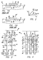
- FIG. 1 a is a side elevational view of one prior art embodiment of a micrometer-scale flash memory;
- FIG. 1b is a view similar to that of FIG. 1a, but of a prior art embodiment of a micrometer-scale flash memory employing a floating gate;
- FIG. 2, on coordinates of current (I) and voltage (V), is a plot depicting the I-V characteristics of a flash memory between the gate and source;
- FIG. 3 is a schematic view of an array of floating-gate field-effect transistors used as a flash memory;
- FIG. 4 is a top plan view of one embodiment of a nanometer-scale flash memory as disclosed herein;
- FIG. 5 is a representation of a transistor comprising a pair of crossed nano-scale wires and a hot electron trap region associated therewith; and
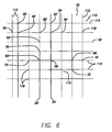
- FIG. 6 is a schematic diagram depicting a crossbar interconnect and showing the features that enable construction of an arbitrarily complex integrated circuit.
- As used herein, the term "self aligned" as applied to "junction" means that the junction that forms the switch and/or other electrical connection between two wires is created wherever two wires, either of which may be coated or functionalized, cross each other, because it is the act of crossing that creates the junction.
- The term "self-assembled" as used herein refers to a system that naturally adopts some geometric pattern because of the identity of the components of the system; the system achieves at least a local minimum in its energy by adopting this configuration.
- The term "singly configurable" means that a switch can change its state only once via an irreversible process such as an oxidation or reduction reaction; such a switch can be the basis of a programmable read only memory (PROM), for example.
- The term "reconfigurable" means that a switch can change its state multiple times via a reversible process such as an oxidation or reduction; in other words, the switch can be opened and closed multiple times such as the memory bits in a random access memory (RAM).
- The term "configurable" means either "singly configurable" or "reconfigurable".
- The term "bi-stable" as applied to a molecule means a molecule having two relatively low energy states. The molecule may be either irreversibly switched from one state to the other (singly configurable) or reversibly switched from one state to the other (reconfigurable).
- Micron-scale dimensions refers to dimensions that range from 1 micrometer to a few micrometers in size.
- Sub-micron scale dimensions refers to dimensions that range from 1 micrometer down to 0.04 micrometers.
- Nanometer scale dimensions refers to dimensions that range from 0.1 nanometers to 50 nanometers (0.05 micrometers).
- Micron-scale and submicron-scale wires refers to rod or ribbon-shaped conductors or semiconductors with widths or diameters having the dimensions of 1 to 10 micrometers, heights that can range from a few tens of nanometers to a micrometer, and lengths of several micrometers and longer.
- A crossbar is an array of switches that connect each wire in one set of parallel wires to every member of a second set of parallel wires that intersects the first set (usually the two sets of wires are perpendicular to each other, but this is not a necessary condition).
- "HOMO" is the common chemical acronym for "highest occupied molecular orbital", while "LUMO" is the common chemical acronym for "lowest unoccupied molecular orbital". HOMOs and LUMOs are responsible for electronic conduction in molecules and the energy difference, or gap (ΔEHOMO/LUMO), between the HOMO and LUMO and other energetically nearby molecular orbitals is responsible for the electronic conduction properties of the molecule.
- Field effect transistors (FETs) are used to construct flash memories. Referring to FIGS. 1a-1b,
such FETs 10, 10' comprise asubstrate 12, in which are formedsource regions 14 anddrain regions 16. Achannel region 18 extends between the source anddrain regions gate 20 is used to control the flow of electrons in thechannel region 18. As depicted in FIG. 1b, thegate 20 is used in combination with afloating gate 22 to control the flow of electrons. It is seen that thesubstrate 12 is of a first polarity, here, p-, and the source anddrain regions - As shown in FIGS. 1a-1b, a flash memory writes a bit by injecting "hot"
electrons 24 into atrap 25, specifically, a dielectric (which may be an oxide layer), associated with the gate 20 (FIG. 1a), or onto the floating gate 22 (FIG. 1b). This injection happens when a voltage threshold is exceeded. - The I-V characteristics of a flash memory are shown in FIG. 2, which shows two curves, one where VT=Hi (Curve 26) and one where VT=Lo (Curve 28). VT is the threshold voltage on the gate at which the transistor starts to conduct. One of these curves,
Curve 26, indicates that hot electrons are present The extra charge between thegate source 14 dictates the properties of the I-V curve. More specifically, if electrons are the carriers in the transistor region (through the channel), then the presence of hot electrons is evidenced bylower Curve 26. If holes are the carriers, then the presence of hot electrons is evidenced byupper Curve 28. - FIG. 3 shows an
array 30 ofFETs 10, with each column connected in series (thesource 14 of oneFET 10 connected to thedrain 16 of an adjacent FET). A plurality of such parallel columns 32 (two are shown, 32a, 32b) are provided. Rows 34 (four are shown, 34a, 34b, 34c, 34d) are created by interconnecting agate 20 of each column 32 to a gate in a neighboring column. - The resulting bit written by injection of a hot electron may be read because of the change in the characteristic current as a function of gate voltage on the associated transistor. A specific bit in the
array 30 may be read by placing a voltage V=Med (a medium voltage) on the selectedrow 34b and V=Hi (a higher voltage) on allother rows gates 20 will pass current freely. The selected transistor with V=Med will pass an amount of current that is a function of the number of hot electrons trapped near itsgate 20. By measuring that current with acurrent sense amp 36 for the selected column, then the value of the bit can be read. - All of the above description is true for existing flash memories. In accordance with an embodiment disclosed herein, a
memory 40 is provided by crossing a plurality of approximately parallelsemiconducting nanowires 42 with a plurality of approximately parallel metallic orsemiconducting nanowires 44, as illustrated in FIG. 4. This creates a two-dimensional array 40 ofnanoscale transistors 110. Next, a hotelectron trap region 120 is provided near enough to eachgate 20 that it influences the switching characteristics of the transistor. Thistrap region 120 is an organic molecule between or near the wires. Thetrap region 120 is considered to be "associated with" thegate 20, within nanometer dimensions. - One example of a molecule advantageously employed as an electron trap in practicing the embodiments disclosed herein comprises a molecule having a structure represented as
I-M-I'.
where M represents a conjugated moiety having a relatively smaller HOMO-LUMO value (to make it effectively metallic-like) and where I and I' represent an insulator portion of the molecule that is connected to thenanoscale wires nanoscale wires - I and I' must be of sufficient length and rigidity to insulate M from the electrode. As an example, I, I' is a long carbon chain moiety that is non-conjugated. Specifically, a carbon chain with greater than about 6 carbon atoms is desirably employed. Such moieties have the requisite higher ΔEHOMO/LUMO value, typically on the order of 3 to 6 eV.
- On the other hand, M, which exhibits metallic-like behavior, is a conjugated moiety, such as, but not limited to, a benzene ring, or two or more fused benzene rings, or polyacetylene. Such moieties have the requisite lower ΔEHOMO/LUMO value, typically on the order of 1 to 2 eV.
- The M moiety should be highly conjugated and relatively compact This compactness consideration tends to favor the aromatic moieties for M over the conjugated alkyne moieties, and thus the aromatic moieties are preferred. Alkynes, being long and thus less rigid than aromatics, are more difficult to control and thus could possible short out the device. The arene rings can be in the molecular plane or perpendicular thereto. An example, depicting I = I' = C8 hydrocarbon chain and two fused benzene rings, is illustrated below:

- While one pair of insulating moieties is shown above, more than one such pair of insulating moieties may be present
- The exposed ends of the I moieties are attached to the
electrodes electrodes - Based on the foregoing description, it is easy for one skilled in the art to construct other I-M-I' configurations that are useful in the practice of the embodiments disclosed herein.
- The I-V characteristics will change, depending on the M moiety. For example, several rings can hold several electrons, compared to one ring. Thus, more rings are preferred, but, as mentioned above, the length of the rings will be a limiting factor to the number of rings. The larger the overall M moiety, the more metallic-like the molecule is in its properties. If the M moiety is relatively small, it takes a greater voltage to place an electron on it; if larger, the HOMO-LUMO gap is smaller and thus it is easier to place an electron on the M moiety. It is desirable to have more than one aromatic ring, but it is possible that with too many rings, shorting of the device could occur. The maximum length of the M moiety ultimately depends on the voltage placed on the
wires - It is also possible to stack the rings, in order to achieve a higher density of hot electron storage. For example,
U.S. Patent 5,287,421 discusses the polyacenes (two or more fused benzene rings), which can be stacked, due to their planar structure. - The molecular species, such as disclosed above, can be, to a first approximation, treated as a capacitor, recognizing that an energy is required to place the electron on the M moiety, or charge the capacitor (the M moiety), which is the same as the energy required to write a bit to memory.
- The energy that the hot electrons must have (how "hot" they must be) is determined by three factors. First, the electrons must have energy greater than the barrier height (in volts) of I or I'. Second, the electrons must have energy greater than the LUMO of the M moiety. Third, the electrons must have energy large enough to charge M treated as one plate of a capacitor, the other plate being the electrode that is the source of the hot electrons. Nanoscale Wire Transistor.
- Another approach for constructing the nanoscale transistor that may be suitably employed herein is that taught in the above-referenced application filed in the names of Philip J. Kuekes et al and entitled "Molecular Wire Transistor". As taught in that application, FETs are fabricated using a cross-bar array, comprising a two-dimensional array of crossed wires, in which one plurality of wires comprises a semiconductor material and the other plurality of wires comprises a metal. The semiconductor wires become the transistor and the metal wires induce formation of a gate in the semiconductor wire. A molecular species at the junction of each wire pair creates a sufficient standoff distance from the metal wire to insulate it from the gate, which is formed between source and drain regions defined by the creation of the gate in the semiconductor wire.
- In yet another embodiment, a memory effect (trapped hot electron considered as a configuration state) may be incorporated into the nanoscale transistor. By providing an electron trap, it then becomes possible to have a special type of transistor. The electron trap comprises the molecular species discussed above.
- If the configuration state is not set (no electrons in the trap), then a transistor is formed, but if the configuration state is set (electrons in the trap), then either an open or closed switch is formed. Whether a switch is open or closed depends on whether the gated region of the transistor conducts with electrons or holes. If the transistor conducts with electrons, then one or more electrons in the trap will form an open switch. If the transistor conducts with holes, then one or more electrons in the trap will form a closed switch.
- In any event, in one embodiment herein, the
first wires 42 and thesecond wires 44 each have a diameter of up to 50 nm and the second wires are separated from the first wires by a distance of up to 50 nm. - The present invention allows transistors to be formed with a size on the order of tens of nanometers to a few nanometers. By choosing a hot electron trap region, associated with each intersection of the first nanowires with the second nanowires, for controlling conductance of the associated transistor, it is possible to build transistors with a wide variety of specifically desired electrical properties. The inclusion of an electrically settable memory bit, through trapping hot electrons near the gate region, allows a new and useful function to be added to transistors.
- An extremely regular and therefore inexpensive assembly process is used to form the nanowires and to form regular arrays of nanowires. For examples of such assembly processes, see the following issued patents, the contents of which are incorporated herein by reference:
U.S. Patent 6,128,214 , entitled "Molecular Wire Crossbar Memory", issued to Philip J. Kuekes et al on October 3, 2000;U.S. Patent 6,248,674 , entitled "Method of Aligning Nanowires", issued to Theodore I. Kamins et al on June 19, 2001;U.S. Patent 6,256,767 , entitled "Demultiplexer for a Molecular Wire Crossbar Network (MWCN DEMUX)", issued to Philip J. Kuekes et al on July 3, 2001;U.S. Patent 6,294,450 , entitled "Nanoscale Patterning for the Formation of Extensive Wires", issued to Yon Chen et al on September 25, 2001; andU.S. Patent 6,314,019 , entitled "Molecular-Wire Crossbar Interconnect (MWCI) for Signal Routing and Communications", issued to Philip J. Kuekes et al on November 6, 2001, all assigned to the same assignee as the present application. - FIG. 5 depicts a
single transistor 110 comprising a pair of crossed nano-scale wires electron trap region 120 disposed in association with thejunction 118 formed by two nano-scale wires. One of the nano-scale wires scale wires scale wires - FIG. 6 represents an embodiment of a
crossbar 50 that employs the configurablemolecular wire transistors 110 disclosed herein. Thecrossbar 50, which is disclosed and claimed inU.S. Patent 6,314,019 , entitled "Molecular-Wire Crossbar Interconnect (MWCI) for Signal Routing and Communications, issued on November 6, 2001, to Philip J. Kuekes et al and assigned to the same assignee as the present application, consists of a layer ofvertical nanowires 112 and a layer ofhorizontal nanowires 114.Junctions 118 are formed where thevertical wires 112 and thehorizontal wires 114 cross. Distinct electrical nets (one indicated by dashedlines 52, one indicated by heavysolid lines 54, and one indicated by dotted lines 56) may be created in thecrossbar 50 as part of an integrated circuit Theseseparate circuits crossbar array 50. Alternatively two or more nets, e.g., 54, 56 may connect to an electronic device 86 (e.g., resonant tunneling diode or transistor) internal to thecrossbar array 50. The electronic device, whether external or internal 86, may comprise a nanoscaleconfigurable transistor 110 herein. - In the circuit depicted in FIG. 6, it is to be understood that all pairs of
wires switch 118 between them open unless it specifically intended to be closed by the design of the integrated circuit The freedom of a circuit designer to arbitrarily select the mixture of device types and interconnect topologies (of which FIG. 6 only shows arbitrary examples) makes the circuit valuable. - The nano-scale flash memory disclosed and claimed herein is expected to find use in nano-scale electronic circuits and as very high density memory.
Claims (28)
- A nano-scale flash memory comprising:(a) source and drain regions in a plurality of approximately parallel first wires (42) of nanometer-scale diameter, said first wires (42) comprising a semiconductor material, said source and drain regions separated by a channel region;(b) gate electrodes in a plurality of approximately parallel second wires (44) of nanometer-scale diameter, said second wires (44) comprising either a semiconductor material or a metal, said second wires (44) crossing said first wires (42) at a closest distance of nanometer scale dimensions between said second wires (44) and said first wires (42), and at a non-zero angle over said channel regions, to form an array of nanoscale transistors (110); and(c) a hot electron trap region (120), associated with each intersection of said first wires (42) with said second wires (44), for controlling conductance of an associated transistor (110),wherein said hot electron trap region (120) comprises an organic molecule configured between said first wires and said second wires or near the intersection thereof.
- The nano-scale flash memory of claim 1 wherein said organic molecule comprises a molecule having the structure represented by
I-M-I'.
where M represents a conjugated moiety having a relatively smaller HOMO-LUMO value and where I and I' represent an Insulator portion of the molecule that Is connected to said first wires and second wires, with I and I' the same or different and having a relatively higher HOMO-LUMO value. - The nano-scale flash memory of claim 2 wherein I, I' is a long carbon chain moiety that is non-conjugated and wherein M is a conjugated moiety.
- The nano-scale flash memory of claim 2 wherein I, I' is a carbon chain of greater than 6 carbon atoms and has a ΔEHOMO/LUMO value of about 3 to 6 eV.
- The nano-scale flash memory of claim 2 wherein M is selected from the group consisting of a benzene ring, polyacenes, and polyacetylene and has a ΔEHOMO/LUMO value of about 1 to 2 eV.
- The nano-scale flash memory of claim 1 wherein said first wires and said second wires each have a diameter of up to 50 nm and where said second wires are separated from said first wires by a distance of up to 50 nm.
- A nano-scale wire transistor (110) comprising (a) a pair of crossed nanowires (112, 114) that form an intersection, one of said nanowires (112, 114) comprising a semiconductor material and another of said nanowires (112, 114) comprising either a metal or a second semiconductor material, said wires (112, 114) crossing at a closest distance of nanometer dimension therebetween and at a non-zero angle, and (b) a hot electron trap region (120) associated with said intersection for controlling conductance of the associated transistor (110), thereby forming a configurable transistor or a switch memory bit that is capable of being set by application of a voltage that is larger in absolute magnitude than any voltage at which said transistor (110) operates,
wherein said hot electron trap region (120) comprises an organic molecule configured between said nanowires or near an intersection thereof. - The nano-scale wire transistor (110) of claim 7 wherein said organic molecule (120) comprises a molecule having the structure represented by
I-M-I'
where M represents a conjugated moiety having a relatively smaller HOMO-LUMO value and where I and I' represent an insulator portion of the molecule that is connected to said first wires and second wires, with I and I' the same or different and having a relatively higher HOMO-LUMO value. - The nano-scale wire transistor (110) of claim 8 wherein I, I' is a long carbon chain moiety that is non-conjugated and wherein M is a conjugated moiety.
- The nano-scale wire transistor (110) of claim 9 wherein I, I' is a carbon chain of greater than 6 carbon atoms and has a ΔEHOMO/LUMO value of about 3 to 6 eV.
- The nano-scale wire transistor (110) of claim 9 wherein M is selected from the group consisting of a benzene ring, polyacenes, and polyacetylene and has a ΔEHOMO/LUMO value of about 1 to 2 eV.
- The nano-scale wire transistor (110) of claim 7 wherein said nanowires (112, 114) each have a diameter of up to 50 nm and where said intersecting nanowires are separated from each other by a distance of up to 50 nm.
- The nano-scale wire transistor (110) of claim 7 wherein said configuration state is not set, thereby forming a transistor.
- The nano-scale wire transistor (110) of claim 7 wherein said configuration state is set, thereby forming either an open or closed switch.
- The nano-scale wire transistor (110) of claim 7 wherein both said nanowires (112, 114) comprise a semiconductor material and wherein both semiconductor materials have the same conductivity.
- The nano-scale wire transistor (110) of claim 7 wherein both said nanowires (112, 114) comprise a semiconductor material and wherein both semiconductor materials have the opposite conductivity.
- A method for fabricating at least one nano-scale wire transistor (110) comprising (a) a pair of crossed nano-wires (112. 114) that form an intersection, one of said nanowires (112, 114) comprising a semiconductor material having a first conductivity and another of said nanowires (112,114) comprising either a metal or a second semiconductor material having a second and opposite conductivity, and (b) a hot electron trap region (120); associated with each intersection of first nanowires with second nanowires, for controlling conductance of the associated transistor (110), said method comprising:(a) providing at least one first nano-wire (112);(b) providing at least one second nano-wire (114), crossing said at least one first wire at a non-zero angle such that the shortest distance between said first wire (112) and said second wire (114) is of nanometer dimensions; and(c) providing a hot electron trap region (120) associated with said transistor (110),wherein said hot electron trap region (120) comprises an organic molecule configured between said nanowires or near the intersection thereof.
- The method of claim 17 wherein said organic molecule comprises a molecule having the structure represented by
I-M-I'.
where M represents a conjugated moiety having a relatively smaller HOMO-LUMO value and where I and I' represent an insulator portion of the molecule that is connected to said first wires and second wires, with I and I' the same or different and having a relatively higher HOMO-LUMO value. - The method of claim 18 wherein I, I' is a long carbon chain moiety that is non-conjugated and wherein M is a conjugated moiety.
- The method of claim 19 wherein I, I' is a carbon chain of greater than 6 carbon atoms and has a ΔEHOMO/LUMO value of about 3 to 6 eV.
- The method of claim 19 wherein M is selected from the group consisting of a benzene ring, polyacenes, and polyacetylene and has a ΔEHOMO/LUMO value of about 1 to 2 eV.
- The method of claim 17 wherein said nanowires (112, 114) each have a diameter of up to 50 nm and where said intersecting nanowires are separated from each other by a distance of up to 50 nm.
- The method of claim 17 wherein said hot electron trap region (120) forms a configurable transistor or a switch memory bit that is capable of being set by application of a voltage that is larger in absolute magnitude than any voltage at which said transistor operates.
- The method of claim 23 wherein said configuration state is not set, thereby forming a transistor.
- The method of claim 23 wherein said configuration state is set, thereby forming either an open or closed switch.
- The method of claim 17 wherein both said nanowires (112, 114) comprise a semiconductor material and wherein both semiconductor materials have the same conductivity.
- The method of claim 17 wherein both said nanowires (112, 114) comprise a semiconductor material and wherein both semiconductor materials have the opposite conductivity.
- A crossbar array of crossed-wire devices, each device comprising a junction formed by a pair of crossed nanowires where one wire crosses another at a non-zero angle, said junction having a functional dimension in nanometers, wherein at least one said junction in said crossbar array comprises a molecular nano-scale wire transistor (110) according to one of claims 7 to 16.
Applications Claiming Priority (3)
| Application Number | Priority Date | Filing Date | Title |
|---|---|---|---|
| US10/138,076 US6760245B2 (en) | 2002-05-01 | 2002-05-01 | Molecular wire crossbar flash memory |
| US138076 | 2002-05-01 | ||
| PCT/US2003/011290 WO2003094171A1 (en) | 2002-05-01 | 2003-04-11 | Molecular wire crossbar flash memory |
Publications (2)
| Publication Number | Publication Date |
|---|---|
| EP1500110A1 EP1500110A1 (en) | 2005-01-26 |
| EP1500110B1 true EP1500110B1 (en) | 2007-06-13 |
Family
ID=29269246
Family Applications (1)
| Application Number | Title | Priority Date | Filing Date |
|---|---|---|---|
| EP03721635A Expired - Fee Related EP1500110B1 (en) | 2002-05-01 | 2003-04-11 | Molecular wire crossbar flash memory |
Country Status (7)
| Country | Link |
|---|---|
| US (1) | US6760245B2 (en) |
| EP (1) | EP1500110B1 (en) |
| JP (1) | JP4767538B2 (en) |
| KR (1) | KR100968380B1 (en) |
| AU (1) | AU2003224938A1 (en) |
| DE (1) | DE60314401T2 (en) |
| WO (1) | WO2003094171A1 (en) |
Families Citing this family (83)
| Publication number | Priority date | Publication date | Assignee | Title |
|---|---|---|---|---|
| US6706402B2 (en) | 2001-07-25 | 2004-03-16 | Nantero, Inc. | Nanotube films and articles |
| AU2003216070A1 (en) * | 2002-01-18 | 2003-09-02 | California Institute Of Technology | Array-based architecture for molecular electronics |
| US6872645B2 (en) * | 2002-04-02 | 2005-03-29 | Nanosys, Inc. | Methods of positioning and/or orienting nanostructures |
| DE60325903D1 (en) * | 2002-07-25 | 2009-03-05 | California Inst Of Techn | Three-dimensional storage array |
| DE60212118T2 (en) * | 2002-08-08 | 2007-01-04 | Sony Deutschland Gmbh | Method for producing a crossbar structure of nanowires |
| EP1563480A4 (en) * | 2002-09-30 | 2010-03-03 | Nanosys Inc | Integrated displays using nanowire transistors |
| JP5336031B2 (en) | 2002-09-30 | 2013-11-06 | ナノシス・インク. | Large area nano-capable macroelectronic substrate and its use |
| US7619562B2 (en) * | 2002-09-30 | 2009-11-17 | Nanosys, Inc. | Phased array systems |
| US7135728B2 (en) * | 2002-09-30 | 2006-11-14 | Nanosys, Inc. | Large-area nanoenabled macroelectronic substrates and uses therefor |
| US7051945B2 (en) * | 2002-09-30 | 2006-05-30 | Nanosys, Inc | Applications of nano-enabled large area macroelectronic substrates incorporating nanowires and nanowire composites |
| US7067867B2 (en) * | 2002-09-30 | 2006-06-27 | Nanosys, Inc. | Large-area nonenabled macroelectronic substrates and uses therefor |
| US6944054B2 (en) * | 2003-03-28 | 2005-09-13 | Nantero, Inc. | NRAM bit selectable two-device nanotube array |
| US7294877B2 (en) | 2003-03-28 | 2007-11-13 | Nantero, Inc. | Nanotube-on-gate FET structures and applications |
| WO2005019793A2 (en) | 2003-05-14 | 2005-03-03 | Nantero, Inc. | Sensor platform using a horizontally oriented nanotube element |
| WO2004109706A2 (en) * | 2003-06-02 | 2004-12-16 | California Institute Of Technology | Nanoscale wire-based sublithographic programmable logic arrays |
| US7242601B2 (en) * | 2003-06-02 | 2007-07-10 | California Institute Of Technology | Deterministic addressing of nanoscale devices assembled at sublithographic pitches |
| US7211854B2 (en) | 2003-06-09 | 2007-05-01 | Nantero, Inc. | Field effect devices having a gate controlled via a nanotube switching element |
| US7274064B2 (en) | 2003-06-09 | 2007-09-25 | Nanatero, Inc. | Non-volatile electromechanical field effect devices and circuits using same and methods of forming same |
| WO2005029498A2 (en) * | 2003-07-24 | 2005-03-31 | California Institute Of Technology | Nanoscale wire coding for stochastic assembly |
| US7289357B2 (en) | 2003-08-13 | 2007-10-30 | Nantero, Inc. | Isolation structure for deflectable nanotube elements |
| WO2005048296A2 (en) | 2003-08-13 | 2005-05-26 | Nantero, Inc. | Nanotube-based switching elements with multiple controls and circuits made from same |
| CN101562049B (en) * | 2003-08-13 | 2012-09-05 | 南泰若股份有限公司 | Nanotube-based switching elements with multiple controls and circuits made thereof |
| EP1508926A1 (en) * | 2003-08-19 | 2005-02-23 | Hitachi, Ltd. | Nanotube transistor device |
| US8025960B2 (en) * | 2004-02-02 | 2011-09-27 | Nanosys, Inc. | Porous substrates, articles, systems and compositions comprising nanofibers and methods of their use and production |
| US20110039690A1 (en) * | 2004-02-02 | 2011-02-17 | Nanosys, Inc. | Porous substrates, articles, systems and compositions comprising nanofibers and methods of their use and production |
| US7553371B2 (en) * | 2004-02-02 | 2009-06-30 | Nanosys, Inc. | Porous substrates, articles, systems and compositions comprising nanofibers and methods of their use and production |
| US7528437B2 (en) * | 2004-02-11 | 2009-05-05 | Nantero, Inc. | EEPROMS using carbon nanotubes for cell storage |
| US7381579B2 (en) * | 2004-02-26 | 2008-06-03 | Samsung Sdi Co., Ltd. | Donor sheet, method of manufacturing the same, method of manufacturing TFT using the donor sheet, and method of manufacturing flat panel display device using the donor sheet |
| US7115971B2 (en) * | 2004-03-23 | 2006-10-03 | Nanosys, Inc. | Nanowire varactor diode and methods of making same |
| CA2564220A1 (en) * | 2004-04-30 | 2005-12-15 | Nanosys, Inc. | Systems and methods for nanowire growth and harvesting |
| US7785922B2 (en) | 2004-04-30 | 2010-08-31 | Nanosys, Inc. | Methods for oriented growth of nanowires on patterned substrates |
| US20050279274A1 (en) * | 2004-04-30 | 2005-12-22 | Chunming Niu | Systems and methods for nanowire growth and manufacturing |
| US7310004B2 (en) * | 2004-05-28 | 2007-12-18 | California Institute Of Technology | Apparatus and method of interconnecting nanoscale programmable logic array clusters |
| US7161403B2 (en) | 2004-06-18 | 2007-01-09 | Nantero, Inc. | Storage elements using nanotube switching elements |
| US7329931B2 (en) * | 2004-06-18 | 2008-02-12 | Nantero, Inc. | Receiver circuit using nanotube-based switches and transistors |
| US7330709B2 (en) * | 2004-06-18 | 2008-02-12 | Nantero, Inc. | Receiver circuit using nanotube-based switches and logic |
| US7652342B2 (en) | 2004-06-18 | 2010-01-26 | Nantero, Inc. | Nanotube-based transfer devices and related circuits |
| US7288970B2 (en) | 2004-06-18 | 2007-10-30 | Nantero, Inc. | Integrated nanotube and field effect switching device |
| US7164744B2 (en) * | 2004-06-18 | 2007-01-16 | Nantero, Inc. | Nanotube-based logic driver circuits |
| AU2005325265A1 (en) * | 2004-07-07 | 2006-07-27 | Nanosys, Inc. | Systems and methods for harvesting and integrating nanowires |
| US8471238B2 (en) | 2004-09-16 | 2013-06-25 | Nantero Inc. | Light emitters using nanotubes and methods of making same |
| US7345307B2 (en) * | 2004-10-12 | 2008-03-18 | Nanosys, Inc. | Fully integrated organic layered processes for making plastic electronics based on conductive polymers and semiconductor nanowires |
| US7473943B2 (en) * | 2004-10-15 | 2009-01-06 | Nanosys, Inc. | Gate configuration for nanowire electronic devices |
| US7309875B2 (en) * | 2004-11-22 | 2007-12-18 | Hewlett-Packard Development Company, L.P. | Nanocrystal protective layer for crossbar molecular electronic devices |
| CA2585009C (en) | 2004-11-24 | 2014-09-30 | Nanosys, Inc. | Contact doping and annealing systems and processes for nanowire thin films |
| US7560366B1 (en) | 2004-12-02 | 2009-07-14 | Nanosys, Inc. | Nanowire horizontal growth and substrate removal |
| US7391090B2 (en) * | 2004-12-17 | 2008-06-24 | Hewlett-Packard Development Company, L.P. | Systems and methods for electrically coupling wires and conductors |
| US7503989B2 (en) * | 2004-12-17 | 2009-03-17 | Hewlett-Packard Development Company, L.P. | Methods and systems for aligning and coupling devices |
| US7521784B2 (en) * | 2004-12-17 | 2009-04-21 | Hewlett-Packard Development Company, L.P. | System for coupling wire to semiconductor region |
| US7429864B2 (en) * | 2004-12-17 | 2008-09-30 | Hewlett-Packard Development Company, L.P. | Systems and methods for rectifying and detecting signals |
| US7598544B2 (en) * | 2005-01-14 | 2009-10-06 | Nanotero, Inc. | Hybrid carbon nanotude FET(CNFET)-FET static RAM (SRAM) and method of making same |
| US8362525B2 (en) | 2005-01-14 | 2013-01-29 | Nantero Inc. | Field effect device having a channel of nanofabric and methods of making same |
| US7447055B2 (en) * | 2005-04-22 | 2008-11-04 | Hewlett-Packard Development Company, L.P. | Multiplexer interface to a nanoscale-crossbar |
| US7394687B2 (en) | 2005-05-09 | 2008-07-01 | Nantero, Inc. | Non-volatile-shadow latch using a nanotube switch |
| US7781862B2 (en) | 2005-05-09 | 2010-08-24 | Nantero, Inc. | Two-terminal nanotube devices and systems and methods of making same |
| TWI324773B (en) | 2005-05-09 | 2010-05-11 | Nantero Inc | Non-volatile shadow latch using a nanotube switch |
| US7479654B2 (en) | 2005-05-09 | 2009-01-20 | Nantero, Inc. | Memory arrays using nanotube articles with reprogrammable resistance |
| CA2609042A1 (en) * | 2005-06-02 | 2006-12-07 | Nanosys, Inc. | Light emitting nanowires for macroelectronics |
| US20070031318A1 (en) * | 2005-08-03 | 2007-02-08 | Jie Liu | Methods of chemically treating an electrically conductive layer having nanotubes therein with diazonium reagent |
| JP2009513368A (en) * | 2005-09-23 | 2009-04-02 | ナノシス・インコーポレイテッド | Method for doping nanostructures |
| KR100967210B1 (en) * | 2005-09-27 | 2010-07-05 | 삼성전자주식회사 | Shape memory device |
| CN101273456B (en) | 2005-09-27 | 2012-04-18 | 康奈尔研究基金公司 | Shape memory device |
| US7741197B1 (en) | 2005-12-29 | 2010-06-22 | Nanosys, Inc. | Systems and methods for harvesting and reducing contamination in nanowires |
| JP2009522197A (en) * | 2005-12-29 | 2009-06-11 | ナノシス・インコーポレイテッド | Method for oriented growth of nanowires on patterned substrates |
| US7405462B2 (en) * | 2006-01-31 | 2008-07-29 | Hewlett-Packard Development Company, L.P. | FPGA architecture at conventional and submicron scales |
| US7763932B2 (en) * | 2006-06-29 | 2010-07-27 | International Business Machines Corporation | Multi-bit high-density memory device and architecture and method of fabricating multi-bit high-density memory devices |
| FR2897978A1 (en) * | 2006-08-03 | 2007-08-31 | Commissariat Energie Atomique | Memory cell for storing e.g. binary information, has field effect memory and access transistors including respective source and drain, where source and drain form additional electrode that is connected to additional control line |
| WO2008057558A2 (en) * | 2006-11-07 | 2008-05-15 | Nanosys, Inc. | Systems and methods for nanowire growth |
| US7786024B2 (en) * | 2006-11-29 | 2010-08-31 | Nanosys, Inc. | Selective processing of semiconductor nanowires by polarized visible radiation |
| GB0801494D0 (en) * | 2007-02-23 | 2008-03-05 | Univ Ind & Acad Collaboration | Nonvolatile memory electronic device using nanowire used as charge channel and nanoparticles used as charge trap and method for manufacturing the same |
| US7492624B2 (en) * | 2007-06-29 | 2009-02-17 | Stmicroelectronics S.R.L. | Method and device for demultiplexing a crossbar non-volatile memory |
| US8395901B2 (en) * | 2007-11-13 | 2013-03-12 | William Marsh Rice University | Vertically-stacked electronic devices having conductive carbon films |
| US20110001117A1 (en) * | 2008-01-21 | 2011-01-06 | President And Fellows Of Harvard College | Nanoscale wire-based memory devices |
| EP2230633A1 (en) | 2009-03-17 | 2010-09-22 | Commissariat à l'Énergie Atomique et aux Énergies Alternatives | Neural network circuit comprising nanoscale synapses and CMOS neurons |
| HUE059099T2 (en) | 2009-05-19 | 2022-10-28 | Oned Mat Inc | Nanostructured materials for battery applications |
| WO2010144092A1 (en) * | 2009-06-12 | 2010-12-16 | Hewlett-Packard Development Company, L.P. | Capacitive crossbar arrays |
| WO2010147588A1 (en) | 2009-06-18 | 2010-12-23 | Hewlett-Packard Development Company, L.P. | Memcapacitor |
| WO2011088340A2 (en) * | 2010-01-15 | 2011-07-21 | Board Of Regents, The University Of Texas System | A carbon nanotube crossbar based nano-architecture |
| CN102214577B (en) * | 2010-04-09 | 2012-12-26 | 中国科学院微电子研究所 | Method for manufacturing nano switch |
| KR101733050B1 (en) | 2010-11-22 | 2017-05-08 | 삼성전자주식회사 | 3-Terminal Resonator and the Method thereof |
| US8879323B2 (en) * | 2012-11-21 | 2014-11-04 | Flashsilicon Incorporation | Interconnection matrix using semiconductor non-volatile memory |
| US9318717B1 (en) * | 2015-01-05 | 2016-04-19 | International Business Machines Corporation | Semi-conductor device with programmable response |
| TWI802275B (en) * | 2022-02-16 | 2023-05-11 | 昱文 李 | System on chip |
Family Cites Families (9)
| Publication number | Priority date | Publication date | Assignee | Title |
|---|---|---|---|---|
| US5287421A (en) * | 1993-01-11 | 1994-02-15 | University Of Southern California | All-optical modulation in crystalline organic semiconductor waveguides |
| US5852306A (en) * | 1997-01-29 | 1998-12-22 | Micron Technology, Inc. | Flash memory with nanocrystalline silicon film floating gate |
| JP3866460B2 (en) | 1998-11-26 | 2007-01-10 | 株式会社東芝 | Nonvolatile semiconductor memory device |
| US6128214A (en) * | 1999-03-29 | 2000-10-03 | Hewlett-Packard | Molecular wire crossbar memory |
| US6459095B1 (en) * | 1999-03-29 | 2002-10-01 | Hewlett-Packard Company | Chemically synthesized and assembled electronics devices |
| US6541309B2 (en) * | 2001-03-21 | 2003-04-01 | Hewlett-Packard Development Company Lp | Fabricating a molecular electronic device having a protective barrier layer |
| US6432740B1 (en) * | 2001-06-28 | 2002-08-13 | Hewlett-Packard Company | Fabrication of molecular electronic circuit by imprinting |
| EP1278234B1 (en) * | 2001-07-19 | 2012-01-11 | STMicroelectronics Srl | MOS transistor and method of manufacturing |
| CA2488172A1 (en) * | 2001-11-06 | 2003-05-15 | Domenico Marzano | Padded envelope |
-
2002
- 2002-05-01 US US10/138,076 patent/US6760245B2/en not_active Expired - Fee Related
-
2003
- 2003-04-11 JP JP2004502301A patent/JP4767538B2/en not_active Expired - Fee Related
- 2003-04-11 WO PCT/US2003/011290 patent/WO2003094171A1/en active IP Right Grant
- 2003-04-11 DE DE60314401T patent/DE60314401T2/en not_active Expired - Lifetime
- 2003-04-11 AU AU2003224938A patent/AU2003224938A1/en not_active Abandoned
- 2003-04-11 KR KR1020047017351A patent/KR100968380B1/en not_active IP Right Cessation
- 2003-04-11 EP EP03721635A patent/EP1500110B1/en not_active Expired - Fee Related
Non-Patent Citations (1)
| Title |
|---|
| None * |
Also Published As
| Publication number | Publication date |
|---|---|
| DE60314401D1 (en) | 2007-07-26 |
| AU2003224938A1 (en) | 2003-11-17 |
| JP2006507660A (en) | 2006-03-02 |
| JP4767538B2 (en) | 2011-09-07 |
| US20030206436A1 (en) | 2003-11-06 |
| DE60314401T2 (en) | 2007-09-20 |
| KR100968380B1 (en) | 2010-07-09 |
| KR20040108760A (en) | 2004-12-24 |
| US6760245B2 (en) | 2004-07-06 |
| WO2003094171A1 (en) | 2003-11-13 |
| EP1500110A1 (en) | 2005-01-26 |
Similar Documents
| Publication | Publication Date | Title |
|---|---|---|
| EP1500110B1 (en) | Molecular wire crossbar flash memory | |
| US8431921B2 (en) | Memristor having a triangular shaped electrode | |
| US6314019B1 (en) | Molecular-wire crossbar interconnect (MWCI) for signal routing and communications | |
| US6891744B2 (en) | Configurable nanoscale crossbar electronic circuits made by electrochemical reaction | |
| JP4499418B2 (en) | Method for manufacturing a molecular electronic device | |
| US6559468B1 (en) | Molecular wire transistor (MWT) | |
| US8445884B2 (en) | Memristor with nanostructure electrodes | |
| JP4643145B2 (en) | Electromechanical 3-trace junction device | |
| US7186380B2 (en) | Transistor and sensors made from molecular materials with electric dipoles | |
| US8004876B2 (en) | Configurable molecular switch array | |
| US6977389B2 (en) | Planar polymer memory device | |
| US8283649B2 (en) | Memristor with a non-planar substrate | |
| US6958270B2 (en) | Methods of fabricating crossbar array microelectronic electrochemical cells | |
| WO2002080290A2 (en) | Bistable molecularr mechanical devices with a band gap change activated by an electric field for electronic switching, gating and memory applications. | |
| JP3802760B2 (en) | Circuit assembly having at least one nanoelectronic element and method of manufacturing the same |
Legal Events
| Date | Code | Title | Description |
|---|---|---|---|
| PUAI | Public reference made under article 153(3) epc to a published international application that has entered the european phase |
Free format text: ORIGINAL CODE: 0009012 |
|
| 17P | Request for examination filed |
Effective date: 20041019 |
|
| AK | Designated contracting states |
Kind code of ref document: A1 Designated state(s): AT BE BG CH CY CZ DE DK EE ES FI FR GB GR HU IE IT LI LU MC NL PT RO SE SI SK TR |
|
| AX | Request for extension of the european patent |
Extension state: AL LT LV MK |
|
| 17Q | First examination report despatched |
Effective date: 20050303 |
|
| GRAP | Despatch of communication of intention to grant a patent |
Free format text: ORIGINAL CODE: EPIDOSNIGR1 |
|
| RIC1 | Information provided on ipc code assigned before grant |
Ipc: G11C 16/04 20060101AFI20061109BHEP Ipc: G11C 13/02 20060101ALI20061109BHEP |
|
| GRAS | Grant fee paid |
Free format text: ORIGINAL CODE: EPIDOSNIGR3 |
|
| GRAA | (expected) grant |
Free format text: ORIGINAL CODE: 0009210 |
|
| AK | Designated contracting states |
Kind code of ref document: B1 Designated state(s): DE |
|
| REF | Corresponds to: |
Ref document number: 60314401 Country of ref document: DE Date of ref document: 20070726 Kind code of ref document: P |
|
| PLBE | No opposition filed within time limit |
Free format text: ORIGINAL CODE: 0009261 |
|
| STAA | Information on the status of an ep patent application or granted ep patent |
Free format text: STATUS: NO OPPOSITION FILED WITHIN TIME LIMIT |
|
| 26N | No opposition filed |
Effective date: 20080314 |
|
| PGFP | Annual fee paid to national office [announced via postgrant information from national office to epo] |
Ref country code: DE Payment date: 20110427 Year of fee payment: 9 |
|
| REG | Reference to a national code |
Ref country code: DE Ref legal event code: R119 Ref document number: 60314401 Country of ref document: DE Effective date: 20121101 |
|
| PG25 | Lapsed in a contracting state [announced via postgrant information from national office to epo] |
Ref country code: DE Free format text: LAPSE BECAUSE OF NON-PAYMENT OF DUE FEES Effective date: 20121101 |