EP1494051A2 - Optical connector for reducing noise - Google Patents
Optical connector for reducing noise Download PDFInfo
- Publication number
- EP1494051A2 EP1494051A2 EP04012338A EP04012338A EP1494051A2 EP 1494051 A2 EP1494051 A2 EP 1494051A2 EP 04012338 A EP04012338 A EP 04012338A EP 04012338 A EP04012338 A EP 04012338A EP 1494051 A2 EP1494051 A2 EP 1494051A2
- Authority
- EP
- European Patent Office
- Prior art keywords
- optical
- housing
- receiving
- shield case
- holder
- Prior art date
- Legal status (The legal status is an assumption and is not a legal conclusion. Google has not performed a legal analysis and makes no representation as to the accuracy of the status listed.)
- Granted
Links
Images


Classifications
-
- G—PHYSICS
- G02—OPTICS
- G02B—OPTICAL ELEMENTS, SYSTEMS OR APPARATUS
- G02B6/00—Light guides; Structural details of arrangements comprising light guides and other optical elements, e.g. couplings
- G02B6/24—Coupling light guides
- G02B6/42—Coupling light guides with opto-electronic elements
- G02B6/4201—Packages, e.g. shape, construction, internal or external details
- G02B6/4274—Electrical aspects
- G02B6/4277—Protection against electromagnetic interference [EMI], e.g. shielding means
-
- G—PHYSICS
- G02—OPTICS
- G02B—OPTICAL ELEMENTS, SYSTEMS OR APPARATUS
- G02B6/00—Light guides; Structural details of arrangements comprising light guides and other optical elements, e.g. couplings
- G02B6/24—Coupling light guides
- G02B6/42—Coupling light guides with opto-electronic elements
- G02B6/4292—Coupling light guides with opto-electronic elements the light guide being disconnectable from the opto-electronic element, e.g. mutually self aligning arrangements
-
- G—PHYSICS
- G02—OPTICS
- G02B—OPTICAL ELEMENTS, SYSTEMS OR APPARATUS
- G02B6/00—Light guides; Structural details of arrangements comprising light guides and other optical elements, e.g. couplings
- G02B6/24—Coupling light guides
- G02B6/42—Coupling light guides with opto-electronic elements
- G02B6/4201—Packages, e.g. shape, construction, internal or external details
- G02B6/4246—Bidirectionally operating package structures
Definitions
- Japanese Patent Application Laid-Open No. 2002-23027 discloses a receptacle 100, as an optical connector for use in said fiber optic communications system. Said optical connector converts the signal light transmitted through the optical fiber cable to an electrical signal, and the electrical signal to an optical signal emitted into the optical fiber cable.
- the module cap 105 has a plate-like shape, and is attached to an opening of the container on an outer wall of the housing 102. When the module cap 105 is attached to the housing 102, the module cap 105 covers the optical transmitting and receiving modules 103, 103, together with the housing 102.
- the photoelectric converter of the optical receiving module of the optical transmitting and receiving modules 103, 103 receives the signal light transmitted from corresponding optical fiber through corresponding sleeve 104. Then, the optical receiving module of the optical transmitting and receiving modules 103 converts the signal to specific electrical signal. Further, in the receptacle 100, the optical transmitting module of the optical transmitting and receiving modules 103, 103 converts an electrical signal to specific signal light and emits the light toward the other sleeve to transmit the light to the other optical fiber through the other sleeve.
- the shield case 106 covers the whole housing 102. Therefore, the openings 111, 112 tend to be large. Therefore, it is difficult for the shield case 106 both to reduce the external noise intruding from out side completely, and to reduce the internal noise being emitted outward completely. Thus, it tends to be difficult for the shield case 106 of the receptacle 100 to completely reduce the electrical noise.
- an optical connector made of insulating synthetic resin, and having a housing for receiving both optical transmitting and receiving modules, said connector comprising:
- the optical connector wherein said shield case is made of sheet metal, wherein a part of one sheet of said sheet metal forming the first holder and a part of the other sheet of said sheet metal forming the second holder overlap with each other.
- the shield case receives only the module case, which receives the optical transmitting and receiving modules. Therefore, an opening of the shield case can be made smaller.
- the partition wall is provided in the shield case. Therefore, electrical noise generated by electrical signals outputted from the optical receiving module is prevented from intruding into the optical transmitting module, and electrical noise generated by electrical signals inputted into the optical transmitting module is prevented from intruding into the optical receiving module.
- the optical fiber cable includes an optical fiber made of light guiding material, and first and second sheath parts for covering the optical fiber.
- Said optical fiber is a well-known multi-mode plastic optical fiber having a core and a clad, of which refractive indexes are different from each other, both of which are arranged coaxially.
- a housing is made of synthetic resin and has a box-like shape. Each plug housing receives the optical fiber cable and the fastened ferrule.
- the ferrule locking member is inserted into the plug housing through the insertion hole.
- the ferrule locking member is fixed to the plug housing by such as engaging.
- the ferrule locking member locks the ferrule to prevent the ferrule from dropping out from the plug housing.
- the receptacle 1 is attached to a printed circuit board 2 (PCB) of various electronic equipment as an auxiliary device as described above.
- the printed circuit board 2 is one of the external electronic parts as described above.
- the printed circuit board 2 has an insulating substrate 3, and a not-shown conductive pattern formed on said substrate 3.
- the conductive pattern is made of conductive metal such as copper, formed in a thin film, and stuck on a surface of the substrate 3.
- a slit 4 with which a latter described earth terminal 20 is engaged, and not-shown holes, through which lead terminals 16a, 16b are inserted, are formed on the printed circuit board 2. These slit 4 and holes 16a, 16b penetrate the printed circuit board 2.
- the optical plug is inserted into the engaging chamber 13.
- the engaging chamber 13 is engaged with the optical plug.
- the container receives the optical receiving device 7a, the optical transmitting device 7b, the module case 8, and one end near the optical plug of a later described holder 19 of the shield case 9.
- the housing 5 includes a not-shown pair of receiving tubes formed on the back wall.
- Each of said pair of receiving tubes has a cylinder-like shape, of which an inner diameter is substantially equal to an outer diameter of the sleeve 6.
- the pair of receiving tubes is continued to the back wall, and penetrates the back wall. Further, each receiving tube communicates the engaging chamber 13 to the container.
- the housing 5 includes a pair of sockets 14, into which an earth terminal is pressed.
- Said sockets 14 are provided on each outer surface of a pair of side walls 12 of the housing 5. Later described earth terminals 20 of the shield case 9 are press-fitted into the sockets 14.
- the optical receiving device 7a and the optical transmitting device 7b are received by the container, while respectively being received by the module case 8.
- the optical receiving device 7a converts the received light to an electrical, and includes a main body 15a received by the module case 8 and a plurality of lead terminals 16a.
- the main body 15a has a flat, plate-like shape with a rectangular shape in a plane view.
- the main body 15a includes a photoelectric converter for receiving the signal light.
- the photoelectric converter faces an end surface of the optical fiber of the optical plug engaged with the housing 5.
- the photoelectric converter converts the signal light received through the optical fiber cable into an electrical signal.
- the optical transmitting device 7b is a device to convert an electrical signal into signal light, and includes a main body 15b received by the module case 8 and a plurality of lead terminals 16b.
- the main body 15b has a flat plate-like shape with a rectangular shape in a plane view.
- the main body 15b includes a photoelectric converter to receive signal light.
- the photoelectric converter faces the end surface of the optical fiber cable of the optical plug.
- the photoelectric converter converts the electric light into the signal light.
- the lead terminal 16b is continued to the main body 15b, and the lead terminal 16b is protruded from the main body 15b.
- the lead terminal 16b is electrically connected to the photoelectric converter.
- the lead terminal 16b is protruded outward (below) from the bottom wall 10 of the housing 5.
- the lead terminal 16b is electrically connected to the conductive pattern of the printed circuit board 2.
- the lead terminals 16a, 16b are arranged (passed through) respectively inside the notches 17. Therefore, when the module case 8 receives the main bodies 15a, 15b, spaces 18 between the notches 17 adjacent to each other are arranged in between the adjacent lead terminals 16a, 16b.
- the module case 8 includes the locating parts located respectively in between the lead terminals 16a, 16b adjacent to each other.
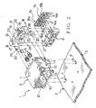
- the shield case 9 is formed by such as bending conductive sheet metal. Namely, the shield case 9 has conductivity. As shown in Fig. 2, the shield case 9 integrally includes a holder 19 having a flat box-like shape and a pair of earth terminals 20. Since the shield case 9 includes the holder 19, the shield case 9 is described to have a box-like shape in this specification. In addition to receiving the module 8, as shown in Figs. 3 and 4, the holder 19 includes a first holder 21, a second holder 22, a partition wall 23 formed in between the first and second holders 21, 22, and an overlapping part 24 (shown in Figs. 6 and 7).
- the first holder 21 and the second holder 22 include a flat box-like shape having an opening 25 at a bottom in the Fig. 2.
- the opening 25 is an opening to make interiors of the holders 21, 22 communicate with exteriors of the holders 21, 22.
- the first holder 21 and the second holder 22 are arranged along a line in which the main bodies 15a, 15b of the optical receiving and transmitting devices 7a, 7b are arranged.
- holder 19 having the above described structure receives the module case 8
- one end at a near side in Fig. 2 of said holder 19 is received in the container of the housing 5. Further, the other end at a far side in Fig. 2 of the holder 19 is exposed to an exterior of the housing 5.
- the partition wall 23 extends in a direction that the module case 8 is inserted into the first and second holders 21, 22 through the opening 25.
- the partition wall 23 partitions a room inside the holder 19 into the first and second holders 21, 22.
- the overlapping part 24 is formed across the first and second holders 21, 22.
- the overlapping part 24 is formed at sleeves 6 side of the holder 19 at a near side in Fig. 2, namely, at the optical plug side. Further, the overlapping part 24 is formed at an edge near the printed circuit board 2, which is arranged at a bottom end in Fig. 2, of the first and second holders 21, 22.
- the overlapping part 24 is formed by a part of one sheet 21a of sheet metal forming the first holder 21, and a part of the other sheet 22a of sheet metal forming the second holder 22, said parts overlapping with each other. Further, said parts of the sheet metals 21a, 22a are in contact with each other at the overlapping part 24.
- the pair of earth terminals 20 is inserted into and engaged with the slits 4 on the printed circuit board 2 to be connected to the conductive pattern of the printed circuit board 2.
- the pair of earth terminals 20 is fixed on the printed circuit board 2 by such as being engaged with the printed circuit board 2.
- the pair of earth terminals 20 electrically connects the shield case 9 to the conductive pattern of the printed circuit board 2.
- the pair of earth terminals 20 electrically connects the shield case 9 to such as an earth circuit through the conductive pattern of the printed circuit board 2. Further, the pair of earth terminals 20 is pressed into sockets 14 to fix the shield case 9 to the housing 5.
- a locking hook 26 for locking the pair of earth terminals 20 in the sockets 14 is formed on the respective earth terminals 20 integrally.
- the shield case 9 presses the sleeves 6 toward the back of the light receiving tubes, namely the back of the housing 5.
- the optical receiving and transmitting devices 7a, 7b are arranged in suitable positions.
- the receptacle 1 is assembled.
- the optical plug is allowed to engage with the receptacle 1.
- the bottom wall 10 is placed on the printed circuit board 2.
- the pair of earth terminals 20 and the lead terminals 16a, 16b are inserted into the slits 4 and the holes on the printed circuit board 2. While the pair of earth terminals 20 is engaged with the slits 4 and connected electrically to the conductive pattern on the printed circuit board 2, the lead terminals 16a, 16b penetrating through the holes are fixed on the conductive pattern of the printed circuit board 2 by such as soldering. thus, the receptacle 1 is attached to the printed circuit board 2.
- the receptacle 1 After the receptacle 1 is attached to the printed circuit board 2, when the optical plug is engaged with the receptacle 1, an electrical signal is supplied to the optical transmitting device 7b through the conductive pattern of the printed circuit board 2.
- the receptacle 1 converts the electrical signal to signal light, and emits the signal light toward one of the optical fibers of the optical plug.
- the receptacle 1 signal light is inputted into the optical receiving device 7a from the other optical fiber of the optical plug.
- the receptacle 1 converts the signal light received by the optical receiving device 7a to an electrical signal, and supplies the electrical signal to the conductive patterns on the printed circuit board 2 through the lead terminal 16a.
- the receptacle 1 converts the signal light from the optical plug to the electrical signal to supply to the printed circuit board 2, and converts the electrical signal from the printed circuit board 2 to the signal light to supply to the optical plug.
- the receptacle 1 discharges electrical noise, which is to intrude into the optical receiving and transmitting devices 7a, 7b from outside, into the earth circuit through the holder 19 of the shield case 9 and the pair of earth terminals 20.
- the receptacle 1 also discharges electrical noise, which is generated by the optical receiving and transmitting devices 7a, 7b, into the earth circuit through the holder 19 of the shield case 9 and the pair of earth terminals 20.
- the external electrical noise is prevented from intruding into the optical receiving and transmitting devices 7a, 7b, and the electrical noise, generated by the optical receiving and transmitting devices 7a, 7b, is prevented from being emitted outward.
- the shield case 9 only receives the module case 8, which receives the main bodies 15a, 15b of the optical receiving and transmitting devices 7a, 7b. Therefore, the opening 25 of the shield case 9 can be made smaller. Therefore, it is hard for the external electrical noise to intrude into the optical receiving and transmitting devices 7a, 7b through the opening 25 of the shield case 9. Further, it is hard for the electrical noise, generated by the optical receiving and transmitting devices 7a, 7b, to be emitted outward through the opening 25. Therefore, the external electrical noise is prevented from intruding into the optical receiving and transmitting devices 7a, 7b, and the electrical noise, generated by the optical receiving and transmitting devices 7a, 7b, can be prevented from being emitted outward.
- Each of locating parts 18 of the module case 8 is located in between the terminals adjacent to each other of the lead terminals 16a, 16b. Therefore, when the lead terminals 16a, 16b start to move in the module case 8, they are blocked by the locating parts 18 to be prevented from moving in the module case 8.
- the lead terminals 16a, 16b can be prevented from rattling in the module case 8, namely in the housing 5, and an electrical connection between these lead terminals 16a, 16b and the printed circuit board 2 as one of external electronic parts can be prevented from being unstable. Therefore, the optical receiving and transmitting devices 7a, 7b can be connected electrically and reliably to the printed circuit board 2. Further, the locating parts 18 prevent the lead terminals 16a, 16b from being in contact with each other. Therefore, the locating parts 18 prevent the lead terminals 16a, 16b from being short-circuited to each other.
- the partition wall 23 is formed on the shield case 9. Therefore, electrical noise, which is generated by electrical signal outputted from the optical receiving device 7a to the printed circuit board 2, is prevented from intruding into the optical transmitting device 7b. Further, electrical noise, which is generated by electrical signal inputted into the optical transmitting device 7b, is prevented from intruding into the optical receiving device 7a. Therefore, electrical noises of the optical receiving and transmitting devices 7a, 7b affecting each other can be reduced to improve cross-talk characteristics of the receptacle 1.
- the receptacle 1 can prevent electrical noise from being emitted outward from an overlapping part 24 where the sheet metals 21a, 22a, forming these holders 21, 22 respectively, overlap with each other. Therefore, the receptacle 1 can reliably prevent the electric noise generated by the optical receiving and transmitting devices 7a, 7b from being emitted outward.
Abstract
Description
- This invention relates to an optical connector to optically interconnect an optical fiber with optical transmitting and receiving modules.
- Generally, a wire harness having a set of electric wires is used for connecting an auxiliary device in a vehicle. Recently, there is a problem that the wire harness increases in size and weight as the number of auxiliary devices and corresponding circuits increase. For solving this problem, a fiber optic communications system, which sends signals to the auxiliary devices by using an optical fiber cable as a part of the wire harness, has been proposed.
- As shown in Fig. 8, Japanese Patent Application Laid-Open No. 2002-23027 discloses a
receptacle 100, as an optical connector for use in said fiber optic communications system. Said optical connector converts the signal light transmitted through the optical fiber cable to an electrical signal, and the electrical signal to an optical signal emitted into the optical fiber cable. - As shown in Fig. 8, a not-shown optical plug (a connector at an optical fiber side), as a mating optical connector, is engaged with
said receptacle 100. Further, thereceptacle 100 is attached to aprinted circuit board 101, which is one of external electronic parts. Thereceptacle 100 includes ahousing 102 made of synthetic resin, optical transmitting andreceiving modules sleeves 104, amodule cap 105 and ashield case 106. - The
housing 102 is made of conductive synthetic resin, and has a box-like shape. Thehousing 102 has a pair of open containers on an outer wall arranged at a far side in Fig. 8. Further, the optical plug as described above is engaged with thehousing 102 at a near side in Fig. 8. - Each of the optical transmitting and
receiving modules main body 107 with a built-in photoelectric converter, and a plurality ofterminals 108 projecting from themain body 107. The container receives themain body 107. When the container receives themain body 107, theterminals 108 project outward from thehousing 102. Theterminals 108 are electrically connected to the photoelectric converter. Theterminals 108 are electrically connected to a not-shown conductive pattern of the printedcircuit board 101. - Each of a pair of
sleeves 104 is made of conductive material, having a cylinder-like shape, and is inserted into a not-shown receiving tube to be attached to thehousing 102. Each of thesleeves 104 has a core and a clad having different indices and being arranged coaxially. - The pair of
sleeves 104 are respectively arranged in between the pair of optical fibers of the optical plug engaged with saidhousing 102 and the photoelectric converters of the pair of optical transmitting andreceiving modules sleeves 104 optically connect the optical fibers to the optical transmitting andreceiving modules - The
module cap 105 has a plate-like shape, and is attached to an opening of the container on an outer wall of thehousing 102. When themodule cap 105 is attached to thehousing 102, themodule cap 105 covers the optical transmitting andreceiving modules housing 102. - The
shield case 106 is made of conductive sheet metal, and includes amain body 109 covering thehousing 102 andlocking projections 110 integrally, saidlocking projections 110 being continued to themain body 109, and projecting from themain body 109 toward the printedcircuit board 101. Themain body 109 has a box-like shape, and a plurality ofopenings - The
housing 102 is inserted into an interior of themain body 109 through one opening 112 of the two openings 111,112. Then, themain body 109 receives thewhole housing 102. When themain body 109 receives thehousing 102, the other opening 111 of themain body 109 overlaps an opening into which the optical plug is inserted. When being locked in ahole 113 on the printedcircuit board 101, thelocking projections 110 are electrically connected to the conductive pattern on the printedcircuit board 101. Further, theshield case 106 is electrically connected to thehousing 102. - The optical plug has the pair of optical fibers and the pair of ferrules, and a plug housing made of synthetic resin. Said pair of optical fibers is arranged in parallel to each other. The optical fibers are covered with the pair of ferrules respectively in a state that end faces of the optical fibers are exposed. While receiving the ferrules, the plug housing engages with the
housing 102. - In the
receptacle 100 having above described structure, when the optical plug is engaged, the photoelectric converter of the optical receiving module of the optical transmitting andreceiving modules corresponding sleeve 104. Then, the optical receiving module of the optical transmitting andreceiving modules 103 converts the signal to specific electrical signal. Further, in thereceptacle 100, the optical transmitting module of the optical transmitting andreceiving modules - Further, the
receptacle 100 guides external electrical noise, which is to intrude into the optical transmitting and receivingmodules main body 109 of theshield case 106 and thehousing 102 to the conductive pattern on the printedcircuit board 101. Theshield case 106 and thehousing 102 prevent the external electrical noise from intruding into the optical transmitting and receivingmodules - Further, the
receptacle 100 guides internal electrical noise, which is generated by the optical transmitting andreceiving modules housing 102 and themain body 109 of theshield case 106 to the conductive pattern on the printedcircuit board 101. Theshield case 106 and thehousing 102 prevent the internal electrical noise from being emitted outward from the optical transmitting and receivingmodules - However, in above described
receptacle 100, theshield case 106 covers thewhole housing 102. Therefore, theopenings shield case 106 both to reduce the external noise intruding from out side completely, and to reduce the internal noise being emitted outward completely. Thus, it tends to be difficult for theshield case 106 of thereceptacle 100 to completely reduce the electrical noise. - Further, the
housing 102 is made of conductive synthetic resin. Therefore, in thereceptacle 100, thehousing 102 cannot be contacted with theterminals 108 of optical transmitting andreceiving modules receptacle 100, theterminals 108 are often not positioned completely to rattle in thehousing 102. There is a fear that after thereceptacle 100 is attached to theprinted circuit board 101, theterminals 108 and the like may be rattled, and electrical connections between theterminals 108, namely the optical transmitting andreceiving modules printed circuit board 101 may become unstable. - Therefore, a first object of this invention is to provide an optical connector which prevents electrical noise from intruding into the optical transmitting and receiving modules, and prevents the internal electrical noise from being emitted outward from the optical transmitting and receiving modules. A second obj ect of this invention is to provide an optical connector, which connects the optical transmitting and receiving modules to external electronic parts reliably and electrically.
- In order to attain the first object, according to this there is provided an optical connector made of insulating synthetic resin, and having a housing for receiving both optical transmitting and receiving modules, said connector comprising:
- a module case made of insulating synthetic resin, and receiving said optical transmitting and receiving modules; and
- a conductive shield case having a box-like shape, and receiving only said module case through an opening thereof, said conductive shield case being attached to said housing.
-
- In order to attain the second object in addition to said first object, according to this invention, there is provided the optical connector,
wherein each of said optical transmitting and receiving modules includes a main body having a photoelectric converter and a plurality of terminals, proj ecting from the main body, being electrically connected to said photoelectric converter,
wherein said module case receives main bodies of said optical transmitting and receiving modules, and includes locating parts to be located in between corresponding terminals of said plurality of terminals adj acent to each other when the main bodies are received by the module case. - According to this invention, preferably, there is provided the optical connector,
wherein said shield case includes a first holder to receive one of said optical transmitting and receiving modules, a second holder to receive the other one of said optical transmitting and receiving modules, and a partition wall arranged between the first and second holders to partition said holders. - According to this invention, preferably, there is provided the optical connector,
wherein said shield case is made of sheet metal,
wherein a part of one sheet of said sheet metal forming the first holder and a part of the other sheet of said sheet metal forming the second holder overlap with each other. - According to the optical connector of this invention, the shield case receives only the module case, which receives the optical transmitting and receiving modules. Therefore, an opening of the shield case can be made smaller.
- According to the optical connector of this invention, each of the locating parts is located in between corresponding terminals adjacent to each other of the optical transmitting and receiving modules. Therefore, when the terminals start to move relative to the module case, the terminals come into contact with the locating parts. Namely, the locating parts prevent the terminals from being in contact with each other.
- According to the optical connector of this invention, the partition wall is provided in the shield case. Therefore, electrical noise generated by electrical signals outputted from the optical receiving module is prevented from intruding into the optical transmitting module, and electrical noise generated by electrical signals inputted into the optical transmitting module is prevented from intruding into the optical receiving module.
- According to the optical connector of this invention, a part of one sheet of the sheet metal forming the first holder and a part of the other sheet of the sheet metal forming the second holder overlap with each other. Therefore, electrical noise is prevented from being emitted outward from an area where the sheets of sheet metal, which form these holders, overlap with each other.
-
- Fig. 1 is a perspective view showing a state where a receptacle as an optical connector according to one embodiment of this invention is attached to a printed circuit board;
- Fig. 2 is an exploded perspective view showing the receptacle according to the one embodiment of this invention;
- Fig. 3 is a sectional view taken along line III-III in Fig. 2, showing a shield case of the receptacle;
- Fig. 4 is a sectional view showing a state where a module case receiving optical transmitting and receiving modules is received by the shield case shown in Fig. 3;
- Fig. 5 is a sectional view taken along line V-V in Fig. 1, showing a relation between locating parts and lead terminals;
- Fig. 6 is an enlarged perspective view of VI in Fig. 2;
- Fig. 7 is a sectional view taken along line VII-VII in Fig. 6; and
- Fig. 8 an exploded perspective view showing a receptacle as a conventional optical connector;
-
- A receptacle (a connector at an electronic equipment side) as an optical connector according to one embodiment of this invention will be explained below with reference to Figs. 1 to 7. A receptacle 1 (the connector at the electronic equipment side) is engaged with an optical plug as a not-shown mating optical connector. Said optical plug includes a pair of optical fibers, a pair of ferrules, and ferrule locking members.
- The optical fiber cable includes an optical fiber made of light guiding material, and first and second sheath parts for covering the optical fiber. Said optical fiber is a well-known multi-mode plastic optical fiber having a core and a clad, of which refractive indexes are different from each other, both of which are arranged coaxially.
- Each of the ferrules is made of synthetic resin. The ferrule has a cylinder-like shape of which an outer diameter changes gradually. Each ferrule is attached to an end of the optical fiber cable. Each ferrule is fastened to the optical fiber cable.
- A housing is made of synthetic resin and has a box-like shape. Each plug housing receives the optical fiber cable and the fastened ferrule.
- Further, an insertion hole penetrates one outer wall of the plug housing. Further, another outer wall of the plug housing includes a resilient locking arm having a locking projection for coupling with the receptacle.
- The ferrule locking member is inserted into the plug housing through the insertion hole. The ferrule locking member is fixed to the plug housing by such as engaging. When being inserted into the plug housing, the ferrule locking member locks the ferrule to prevent the ferrule from dropping out from the plug housing.
- The receptacle 1 is attached to a printed circuit board 2 (PCB) of various electronic equipment as an auxiliary device as described above. The printed
circuit board 2 is one of the external electronic parts as described above. As shown in Figs. 1 and 2, the printedcircuit board 2 has an insulatingsubstrate 3, and a not-shown conductive pattern formed on saidsubstrate 3. The conductive pattern is made of conductive metal such as copper, formed in a thin film, and stuck on a surface of thesubstrate 3. - Further, a
slit 4, with which a latter describedearth terminal 20 is engaged, and not-shown holes, through which leadterminals circuit board 2. Theseslit 4 andholes circuit board 2. - As shown in Fig. 2, the receptacle 1 includes a
housing 5 made of synthetic resin, a pair of sleeves 6, anoptical receiving device 7a as a fiber optical module (Fiber Optic Transceiver : FOT), an optical transmitdevice 7b as a fiber optical module (Fiber Optic Transceiver : FOT), amodule case 8, and ashield case 9. - The
housing 5 is made of synthetic resin, and as shown in Figs. 1 and 2, has a box-like shape (tube-like shape), including abottom wall 10 arranged along the printedcircuit board 2, aceiling wall 11 facing thebottom wall 10 with a specific space, a pair ofside walls 12 facing to each other with a specific space, each of said pair ofside walls 12 being continued to both thebottom wall 10 and theceiling wall 11, and a not-shown back wall continued to back ends of thesewalls housing 5. The back wall partitions (separates) an inner space of thehousing 5 into an engagingchamber 13 at near side and a container at far side of Figs. 1 and 2. - The optical plug is inserted into the engaging
chamber 13. The engagingchamber 13 is engaged with the optical plug. The container receives theoptical receiving device 7a, theoptical transmitting device 7b, themodule case 8, and one end near the optical plug of a later describedholder 19 of theshield case 9. - Further, the
housing 5 includes a not-shown pair of receiving tubes formed on the back wall. Each of said pair of receiving tubes has a cylinder-like shape, of which an inner diameter is substantially equal to an outer diameter of the sleeve 6. The pair of receiving tubes is continued to the back wall, and penetrates the back wall. Further, each receiving tube communicates the engagingchamber 13 to the container. - Further, the
housing 5 includes a pair ofsockets 14, into which an earth terminal is pressed. Saidsockets 14 are provided on each outer surface of a pair ofside walls 12 of thehousing 5. Later describedearth terminals 20 of theshield case 9 are press-fitted into thesockets 14. - The
optical receiving device 7a and theoptical transmitting device 7b are received by the container, while respectively being received by themodule case 8. Theoptical receiving device 7a converts the received light to an electrical, and includes amain body 15a received by themodule case 8 and a plurality oflead terminals 16a. - The
main body 15a has a flat, plate-like shape with a rectangular shape in a plane view. Themain body 15a includes a photoelectric converter for receiving the signal light. When theoptical receiving device 7a is received by the container while being received by themodule case 8, the photoelectric converter faces an end surface of the optical fiber of the optical plug engaged with thehousing 5. The photoelectric converter converts the signal light received through the optical fiber cable into an electrical signal. - One end of the
lead terminal 16a is continued to themain body 15a, and thelead terminal 16a is protruded from themain body 15a. Thelead terminal 16a is electrically connected to the photoelectric converter. When the container receives theoptical receiving device 7a, thelead terminal 16a is protruded outward (below) from thebottom wall 10 of thehousing 5. When the receptacle 1 is attached to the printedcircuit board 2, thelead terminal 16a is electrically connected to the conductive pattern of the printedcircuit board 2. - The
optical transmitting device 7b is a device to convert an electrical signal into signal light, and includes amain body 15b received by themodule case 8 and a plurality oflead terminals 16b. - The
main body 15b has a flat plate-like shape with a rectangular shape in a plane view. Themain body 15b includes a photoelectric converter to receive signal light. When theoptical transmitting device 7b is received by the container while being received by themodule case 8, the photoelectric converter faces the end surface of the optical fiber cable of the optical plug. The photoelectric converter converts the electric light into the signal light. - One end of the
lead terminal 16b is continued to themain body 15b, and thelead terminal 16b is protruded from themain body 15b. Thelead terminal 16b is electrically connected to the photoelectric converter. When the container receives theoptical transmitting device 7b, thelead terminal 16b is protruded outward (below) from thebottom wall 10 of thehousing 5. When the receptacle 1 is attached to the printedcircuit board 2, thelead terminal 16b is electrically connected to the conductive pattern of the printedcircuit board 2. - Each of the pair of sleeves 6 has a column-like shape, of which an outer diameter is substantially equal to an inner diameter of each receiving tube. Each sleeve 6 includes a light guide (also referred to as "wave guide") to transmit signal light. Each sleeve 6 is received by the light receiving tube, and connects the optical fiber cable of the optical plug to corresponding one of the photoelectric converters of the receiving and transmitting
devices - The
module case 8 is made of synthetic resin, and includes a flat box-like shape having anopening 27 at the back in Fig. 2. The optical receiving and transmittingdevices module case 8 through theopening 27. Themodule case 8 only receives themain bodies devices - Further, as shown in Fig. 5, a plurality of
notches 17 are formed on themodule case 8. Thesenotches 17 are formed by notching an edge of themodule case 8 at theopening 27 side, namely, at a far side of the optical plug. Thenotches 17 are arranged along a line in which thelead terminals - When the
module case 8 receives the optical receiving and transmittingdevices lead terminals notches 17. Therefore, when themodule case 8 receives themain bodies spaces 18 between thenotches 17 adjacent to each other are arranged in between theadjacent lead terminals - The
spaces 18 between thenotches 17 adjacent to each other correspond to the locating parts in this specification, and hereinafter are referred to as the locating parts. According to above, as shown in Fig. 5, themodule case 8 includes the locating parts located respectively in between thelead terminals - The
shield case 9 is formed by such as bending conductive sheet metal. Namely, theshield case 9 has conductivity. As shown in Fig. 2, theshield case 9 integrally includes aholder 19 having a flat box-like shape and a pair ofearth terminals 20. Since theshield case 9 includes theholder 19, theshield case 9 is described to have a box-like shape in this specification. In addition to receiving themodule 8, as shown in Figs. 3 and 4, theholder 19 includes afirst holder 21, asecond holder 22, apartition wall 23 formed in between the first andsecond holders - The
first holder 21 and thesecond holder 22 include a flat box-like shape having anopening 25 at a bottom in the Fig. 2. Theopening 25 is an opening to make interiors of theholders holders first holder 21 and thesecond holder 22 are arranged along a line in which themain bodies devices - Only the
module case 8 receiving the optical receiving and transmittingdevices second holders holder 19 of theshield case 9. The first andsecond holders holder 19 of theshield case 9 only receive themodule case 8 which only receives themain bodies devices first holder 21 receives one of the optical receiving and transmittingdevices main body 15a of the optical. receivingdevice 7a). Thesecond holder 22 receives the other one of the optical receiving and transmittingdevices main body 15b of theoptical transmitting device 7b). - While the
holder 19 having the above described structure receives themodule case 8, one end at a near side in Fig. 2 of saidholder 19 is received in the container of thehousing 5. Further, the other end at a far side in Fig. 2 of theholder 19 is exposed to an exterior of thehousing 5. - The
partition wall 23 extends in a direction that themodule case 8 is inserted into the first andsecond holders opening 25. Thepartition wall 23 partitions a room inside theholder 19 into the first andsecond holders - As shown in Fig. 6, the overlapping
part 24 is formed across the first andsecond holders part 24 is formed at sleeves 6 side of theholder 19 at a near side in Fig. 2, namely, at the optical plug side. Further, the overlappingpart 24 is formed at an edge near the printedcircuit board 2, which is arranged at a bottom end in Fig. 2, of the first andsecond holders part 24 is formed by a part of onesheet 21a of sheet metal forming thefirst holder 21, and a part of theother sheet 22a of sheet metal forming thesecond holder 22, said parts overlapping with each other. Further, said parts of thesheet metals part 24. - A pair of
earth terminals 20 is provided respectively on both edges of theholder 19 in a direction that themain bodies holder 19. The pair ofearth terminals 20 has a blade-like shape extending respectively from the both edges of theholder 19 toward the printedcircuit board 2. When theholder 19 of theshield case 9 is received by the container of thehousing 5, the pair ofearth terminals 20 is protruded from thebottom wall 10 toward a lower side of thehousing 5, namely toward the printedcircuit board 2. - The pair of
earth terminals 20 is inserted into and engaged with theslits 4 on the printedcircuit board 2 to be connected to the conductive pattern of the printedcircuit board 2. The pair ofearth terminals 20 is fixed on the printedcircuit board 2 by such as being engaged with the printedcircuit board 2. The pair ofearth terminals 20 electrically connects theshield case 9 to the conductive pattern of the printedcircuit board 2. The pair ofearth terminals 20 electrically connects theshield case 9 to such as an earth circuit through the conductive pattern of the printedcircuit board 2. Further, the pair ofearth terminals 20 is pressed intosockets 14 to fix theshield case 9 to thehousing 5. - Further, a locking
hook 26 for locking the pair ofearth terminals 20 in thesockets 14 is formed on therespective earth terminals 20 integrally. By the lockinghook 26 locking the pair ofearth terminals 20 in thesockets 14, the pair ofearth terminals 20 fixes theshield case 9 to thehousing 5. - The receptacle 1 having the above described structure is assembled as follows. A part of the sleeves 6 are inserted halfway into the light receiving tubes of the
housing 5. Themain bodies devices module case 8 through theopening 27. At this moment, each of locatingparts 18 of themodule case 8 is located in between the terminals adjacent to each other of thelead terminals module case 8 receives themain bodies devices - The
module case 8 receiving themain bodies second holders shield case 9 through theopening 25. The pair ofearth terminals 20 is pressed into thesockets 14. The locking hooks 26 lock the pair ofearth terminals 20 in thesockets 14. While theholder 19 is received inside the container of thehousing 5, theshield case 9 is fixed to thehousing 5. - Further, when the pair of
earth terminals 20 is pressed into thesockets 14 to fix theshield case 9 to thehousing 5, theshield case 9 presses the sleeves 6 toward the back of the light receiving tubes, namely the back of thehousing 5. Thus, the optical receiving and transmittingdevices - In this manner, the receptacle 1 is assembled. In this condition, the optical plug is allowed to engage with the receptacle 1. Further, for attaching the receptacle 1 to the printed
circuit board 2, firstly thebottom wall 10 is placed on the printedcircuit board 2. The pair ofearth terminals 20 and thelead terminals slits 4 and the holes on the printedcircuit board 2. While the pair ofearth terminals 20 is engaged with theslits 4 and connected electrically to the conductive pattern on the printedcircuit board 2, thelead terminals circuit board 2 by such as soldering. thus, the receptacle 1 is attached to the printedcircuit board 2. - After the receptacle 1 is attached to the printed
circuit board 2, when the optical plug is engaged with the receptacle 1, an electrical signal is supplied to theoptical transmitting device 7b through the conductive pattern of the printedcircuit board 2. The receptacle 1 converts the electrical signal to signal light, and emits the signal light toward one of the optical fibers of the optical plug. - In the receptacle 1, signal light is inputted into the
optical receiving device 7a from the other optical fiber of the optical plug. The receptacle 1 converts the signal light received by theoptical receiving device 7a to an electrical signal, and supplies the electrical signal to the conductive patterns on the printedcircuit board 2 through thelead terminal 16a. Thus, the receptacle 1 converts the signal light from the optical plug to the electrical signal to supply to the printedcircuit board 2, and converts the electrical signal from the printedcircuit board 2 to the signal light to supply to the optical plug. - Further, the receptacle 1 discharges electrical noise, which is to intrude into the optical receiving and transmitting
devices holder 19 of theshield case 9 and the pair ofearth terminals 20. The receptacle 1 also discharges electrical noise, which is generated by the optical receiving and transmittingdevices holder 19 of theshield case 9 and the pair ofearth terminals 20. Thus, the external electrical noise is prevented from intruding into the optical receiving and transmittingdevices devices - According to this embodiment, the
shield case 9 only receives themodule case 8, which receives themain bodies devices opening 25 of theshield case 9 can be made smaller. Therefore, it is hard for the external electrical noise to intrude into the optical receiving and transmittingdevices opening 25 of theshield case 9. Further, it is hard for the electrical noise, generated by the optical receiving and transmittingdevices opening 25. Therefore, the external electrical noise is prevented from intruding into the optical receiving and transmittingdevices devices - Each of locating
parts 18 of themodule case 8 is located in between the terminals adjacent to each other of thelead terminals lead terminals module case 8, they are blocked by the locatingparts 18 to be prevented from moving in themodule case 8. - Therefore, the
lead terminals module case 8, namely in thehousing 5, and an electrical connection between theselead terminals circuit board 2 as one of external electronic parts can be prevented from being unstable. Therefore, the optical receiving and transmittingdevices circuit board 2. Further, the locatingparts 18 prevent thelead terminals parts 18 prevent thelead terminals - The
partition wall 23 is formed on theshield case 9. Therefore, electrical noise, which is generated by electrical signal outputted from theoptical receiving device 7a to the printedcircuit board 2, is prevented from intruding into theoptical transmitting device 7b. Further, electrical noise, which is generated by electrical signal inputted into theoptical transmitting device 7b, is prevented from intruding into theoptical receiving device 7a. Therefore, electrical noises of the optical receiving and transmittingdevices - At the overlapping
part 24, a part of thesheet metal 21a forming thefirst holder 21 and a part of thesheet metal 22a forming thesecond holder 22 overlap with each other. Therefore, the receptacle 1 can prevent electrical noise from being emitted outward from an overlappingpart 24 where thesheet metals holders devices - The embodiments described above only illustrate representative embodiments, and this invention is not limited to these embodiments. Namely, this invention may be employed in various and numerous embodiments without departing from the scope of the invention.
Claims (4)
- An optical connector made of insulating synthetic resin, and having a housing which receives both optical transmitting and receiving modules, said optical connector comprising:a module case made of insulating synthetic resin, and receiving said optical transmitting and receiving modules; anda conductive shield case having a box-like shape, and receiving only said module case through an opening thereof, said conductive shield case being attached to said housing.
- The optical connector as claimed in claim 1,
wherein each of said optical transmitting and receiving modules includes a main body having a photoelectric converter and a plurality of terminals, proj ecting from the main body, being electrically connected to said photoelectric converter,
wherein said module case receives main bodies of said optical transmitting and receiving modules, and includes locating parts to be located between corresponding terminals of said plurality of terminals adjacent to each other when said main bodies are received by the module case. - The optical connector as claimed in claim 1 or 2,
wherein said shield case includes a first holder to receive one of said optical transmitting and receiving modules, a second holder to receive the other one of said optical transmitting and receiving modules, and a partition wall arranged between the first and second holders to partition said holders. - The optical connector as claimed in claim 3,
wherein said shield case is made of sheet metal,
wherein a part of one sheet of said sheet metal forming the first holder and a part of the other sheet of said sheet metal forming the second holder overlap with each other.
Priority Applications (1)
| Application Number | Priority Date | Filing Date | Title |
|---|---|---|---|
| EP08017825A EP2017661A1 (en) | 2003-07-03 | 2004-05-25 | Optical connector for reducing noise |
Applications Claiming Priority (2)
| Application Number | Priority Date | Filing Date | Title |
|---|---|---|---|
| JP2003190904 | 2003-07-03 | ||
| JP2003190904A JP4256728B2 (en) | 2003-07-03 | 2003-07-03 | Optical connector |
Related Child Applications (2)
| Application Number | Title | Priority Date | Filing Date |
|---|---|---|---|
| EP08017825A Division EP2017661A1 (en) | 2003-07-03 | 2004-05-25 | Optical connector for reducing noise |
| EP08017825.4 Division-Into | 2008-10-10 |
Publications (3)
| Publication Number | Publication Date |
|---|---|
| EP1494051A2 true EP1494051A2 (en) | 2005-01-05 |
| EP1494051A3 EP1494051A3 (en) | 2006-01-11 |
| EP1494051B1 EP1494051B1 (en) | 2012-12-12 |
Family
ID=33432341
Family Applications (2)
| Application Number | Title | Priority Date | Filing Date |
|---|---|---|---|
| EP04012338A Expired - Fee Related EP1494051B1 (en) | 2003-07-03 | 2004-05-25 | Optical connector for reducing noise |
| EP08017825A Withdrawn EP2017661A1 (en) | 2003-07-03 | 2004-05-25 | Optical connector for reducing noise |
Family Applications After (1)
| Application Number | Title | Priority Date | Filing Date |
|---|---|---|---|
| EP08017825A Withdrawn EP2017661A1 (en) | 2003-07-03 | 2004-05-25 | Optical connector for reducing noise |
Country Status (3)
| Country | Link |
|---|---|
| US (1) | US7104705B2 (en) |
| EP (2) | EP1494051B1 (en) |
| JP (1) | JP4256728B2 (en) |
Families Citing this family (10)
| Publication number | Priority date | Publication date | Assignee | Title |
|---|---|---|---|---|
| KR100456272B1 (en) * | 2002-11-13 | 2004-11-09 | 양관숙 | Optical contact module |
| JP2005006228A (en) * | 2003-06-13 | 2005-01-06 | Casio Comput Co Ltd | Projector |
| US7128475B2 (en) * | 2004-10-28 | 2006-10-31 | Schweitzer Engineering Laboratories, Inc. | Fiber optic connector |
| JP4413238B2 (en) * | 2007-03-02 | 2010-02-10 | 株式会社オートネットワーク技術研究所 | Vehicle network system |
| JP5095579B2 (en) * | 2008-10-24 | 2012-12-12 | 矢崎総業株式会社 | Optical connector |
| JP5162500B2 (en) | 2009-03-06 | 2013-03-13 | アルプス電気株式会社 | Optical connector with shield |
| JP5690510B2 (en) * | 2010-06-28 | 2015-03-25 | 矢崎総業株式会社 | Electronic components |
| JP2012053246A (en) * | 2010-09-01 | 2012-03-15 | Auto Network Gijutsu Kenkyusho:Kk | Board-mounting type optical connector |
| JP5727259B2 (en) * | 2011-02-28 | 2015-06-03 | 矢崎総業株式会社 | Optical module |
| JP2017009727A (en) * | 2015-06-19 | 2017-01-12 | 矢崎総業株式会社 | Optical connector |
Citations (5)
| Publication number | Priority date | Publication date | Assignee | Title |
|---|---|---|---|---|
| US6213651B1 (en) * | 1999-05-26 | 2001-04-10 | E20 Communications, Inc. | Method and apparatus for vertical board construction of fiber optic transmitters, receivers and transceivers |
| EP1102097A2 (en) * | 1999-11-19 | 2001-05-23 | Yazaki Corporation | Hybrid connector |
| EP1217407A2 (en) * | 2000-12-20 | 2002-06-26 | The Furukawa Electric Co., Ltd. | Optical/electric composite connector |
| EP1255143A2 (en) * | 2001-04-27 | 2002-11-06 | The Furukawa Electric Co., Ltd. | Optical fiber connector |
| US6499889B1 (en) * | 1999-12-08 | 2002-12-31 | Yazaki Corporation | Method of assembling optical connector, optical connector and hybrid connector |
Family Cites Families (5)
| Publication number | Priority date | Publication date | Assignee | Title |
|---|---|---|---|---|
| FR2652229B1 (en) * | 1989-09-19 | 1991-11-15 | Bull Sa | SHIELDING ASSEMBLY FOR A COLLECTOR BLOCK CONNECTED TO ELECTRICAL EQUIPMENT PLACED INSIDE A CHASSIS. |
| JP3646979B2 (en) * | 1999-12-08 | 2005-05-11 | 矢崎総業株式会社 | Hybrid connector |
| JP2002023027A (en) | 2000-07-07 | 2002-01-23 | Yazaki Corp | Optical connector |
| JP4299958B2 (en) * | 2000-07-31 | 2009-07-22 | 富士通株式会社 | Communication device and plug-in unit |
| US6607308B2 (en) * | 2001-02-12 | 2003-08-19 | E20 Communications, Inc. | Fiber-optic modules with shielded housing/covers having mixed finger types |
-
2003
- 2003-07-03 JP JP2003190904A patent/JP4256728B2/en not_active Expired - Fee Related
-
2004
- 2004-05-18 US US10/847,458 patent/US7104705B2/en not_active Expired - Fee Related
- 2004-05-25 EP EP04012338A patent/EP1494051B1/en not_active Expired - Fee Related
- 2004-05-25 EP EP08017825A patent/EP2017661A1/en not_active Withdrawn
Patent Citations (5)
| Publication number | Priority date | Publication date | Assignee | Title |
|---|---|---|---|---|
| US6213651B1 (en) * | 1999-05-26 | 2001-04-10 | E20 Communications, Inc. | Method and apparatus for vertical board construction of fiber optic transmitters, receivers and transceivers |
| EP1102097A2 (en) * | 1999-11-19 | 2001-05-23 | Yazaki Corporation | Hybrid connector |
| US6499889B1 (en) * | 1999-12-08 | 2002-12-31 | Yazaki Corporation | Method of assembling optical connector, optical connector and hybrid connector |
| EP1217407A2 (en) * | 2000-12-20 | 2002-06-26 | The Furukawa Electric Co., Ltd. | Optical/electric composite connector |
| EP1255143A2 (en) * | 2001-04-27 | 2002-11-06 | The Furukawa Electric Co., Ltd. | Optical fiber connector |
Also Published As
| Publication number | Publication date |
|---|---|
| JP2005024944A (en) | 2005-01-27 |
| EP2017661A1 (en) | 2009-01-21 |
| US7104705B2 (en) | 2006-09-12 |
| EP1494051A3 (en) | 2006-01-11 |
| EP1494051B1 (en) | 2012-12-12 |
| JP4256728B2 (en) | 2009-04-22 |
| US20050002620A1 (en) | 2005-01-06 |
Similar Documents
| Publication | Publication Date | Title |
|---|---|---|
| US6783283B2 (en) | Optical connector for coupling optical signals to optical devices | |
| JP3646979B2 (en) | Hybrid connector | |
| EP1217407B1 (en) | Optical/electric composite connector | |
| US6357931B1 (en) | Hybrid connector | |
| JP3735011B2 (en) | Assembly method of hybrid connector | |
| US7111994B2 (en) | Integral insert molded fiber optic transceiver electromagnetic interference shield | |
| US8195017B2 (en) | Consumer input/output (CIO) optical transceiver module for use in an active optical cable, an active optical cable that incorporates the CIO optical transceiver module, and a method | |
| EP1170612B1 (en) | Hybrid optical and electrical connector | |
| JP2010181885A (en) | Small form factor pluggable (sfp) optical transceiver module and method | |
| EP1494051B1 (en) | Optical connector for reducing noise | |
| JP3778479B2 (en) | Light emitting element module, light receiving element module positioning method, optical connector, and hybrid connector | |
| US7090410B2 (en) | Optical receptacle with low transmission loss and photoelectric conversion module for the same | |
| CN111897060B (en) | Optical module | |
| CN111133353B (en) | Optical connector device | |
| US7377702B2 (en) | Cageless, pluggable optoelectronic device which enables belly-to-belly layouts | |
| EP1256828B1 (en) | Connector device and connector | |
| JP3654574B2 (en) | Hybrid connector support structure | |
| EP1170613B1 (en) | Optical connector | |
| JP2015500517A (en) | Optical module | |
| US20180196202A1 (en) | Optical Connector and Branch Structure of Wire Harness | |
| JP2002023025A (en) | Optical connector | |
| EP1102099A2 (en) | Hybrid connector | |
| JP2002023027A (en) | Optical connector | |
| CN111108421B (en) | Optical connector device | |
| JP2002182075A (en) | Structure for fitting optical connector |
Legal Events
| Date | Code | Title | Description |
|---|---|---|---|
| PUAI | Public reference made under article 153(3) epc to a published international application that has entered the european phase |
Free format text: ORIGINAL CODE: 0009012 |
|
| AK | Designated contracting states |
Kind code of ref document: A2 Designated state(s): AT BE BG CH CY CZ DE DK EE ES FI FR GB GR HU IE IT LI LU MC NL PL PT RO SE SI SK TR |
|
| AX | Request for extension of the european patent |
Extension state: AL HR LT LV MK |
|
| PUAL | Search report despatched |
Free format text: ORIGINAL CODE: 0009013 |
|
| AK | Designated contracting states |
Kind code of ref document: A3 Designated state(s): AT BE BG CH CY CZ DE DK EE ES FI FR GB GR HU IE IT LI LU MC NL PL PT RO SE SI SK TR |
|
| AX | Request for extension of the european patent |
Extension state: AL HR LT LV MK |
|
| 17P | Request for examination filed |
Effective date: 20060209 |
|
| AKX | Designation fees paid |
Designated state(s): DE |
|
| RAP1 | Party data changed (applicant data changed or rights of an application transferred) |
Owner name: YAZAKI CORPORATION |
|
| GRAP | Despatch of communication of intention to grant a patent |
Free format text: ORIGINAL CODE: EPIDOSNIGR1 |
|
| GRAS | Grant fee paid |
Free format text: ORIGINAL CODE: EPIDOSNIGR3 |
|
| GRAA | (expected) grant |
Free format text: ORIGINAL CODE: 0009210 |
|
| AK | Designated contracting states |
Kind code of ref document: B1 Designated state(s): DE |
|
| REG | Reference to a national code |
Ref country code: DE Ref legal event code: R096 Ref document number: 602004040360 Country of ref document: DE Effective date: 20130207 |
|
| PLBE | No opposition filed within time limit |
Free format text: ORIGINAL CODE: 0009261 |
|
| STAA | Information on the status of an ep patent application or granted ep patent |
Free format text: STATUS: NO OPPOSITION FILED WITHIN TIME LIMIT |
|
| 26N | No opposition filed |
Effective date: 20130913 |
|
| REG | Reference to a national code |
Ref country code: DE Ref legal event code: R097 Ref document number: 602004040360 Country of ref document: DE Effective date: 20130913 |
|
| PGFP | Annual fee paid to national office [announced via postgrant information from national office to epo] |
Ref country code: DE Payment date: 20140521 Year of fee payment: 11 |
|
| REG | Reference to a national code |
Ref country code: DE Ref legal event code: R119 Ref document number: 602004040360 Country of ref document: DE |
|
| PG25 | Lapsed in a contracting state [announced via postgrant information from national office to epo] |
Ref country code: DE Free format text: LAPSE BECAUSE OF NON-PAYMENT OF DUE FEES Effective date: 20151201 |