EP1475845A1 - Ohmic contacts using Ni-based solid solution for p-type GaN in LEDs - Google Patents
Ohmic contacts using Ni-based solid solution for p-type GaN in LEDs Download PDFInfo
- Publication number
- EP1475845A1 EP1475845A1 EP04251791A EP04251791A EP1475845A1 EP 1475845 A1 EP1475845 A1 EP 1475845A1 EP 04251791 A EP04251791 A EP 04251791A EP 04251791 A EP04251791 A EP 04251791A EP 1475845 A1 EP1475845 A1 EP 1475845A1
- Authority
- EP
- European Patent Office
- Prior art keywords
- solid solution
- group
- electrode layer
- thin film
- gallium nitride
- Prior art date
- Legal status (The legal status is an assumption and is not a legal conclusion. Google has not performed a legal analysis and makes no representation as to the accuracy of the status listed.)
- Granted
Links
- 239000006104 solid solution Substances 0.000 title claims abstract description 78
- PXHVJJICTQNCMI-UHFFFAOYSA-N Nickel Chemical compound [Ni] PXHVJJICTQNCMI-UHFFFAOYSA-N 0.000 claims abstract description 107
- JMASRVWKEDWRBT-UHFFFAOYSA-N Gallium nitride Chemical compound [Ga]#N JMASRVWKEDWRBT-UHFFFAOYSA-N 0.000 claims abstract description 81
- 229910002601 GaN Inorganic materials 0.000 claims abstract description 76
- 229910052759 nickel Inorganic materials 0.000 claims abstract description 37
- 238000000151 deposition Methods 0.000 claims abstract description 31
- 238000000034 method Methods 0.000 claims abstract description 29
- 239000004065 semiconductor Substances 0.000 claims abstract description 13
- 239000010409 thin film Substances 0.000 claims description 44
- 238000000137 annealing Methods 0.000 claims description 32
- 229910052737 gold Inorganic materials 0.000 claims description 29
- 229910052751 metal Inorganic materials 0.000 claims description 26
- 239000002184 metal Substances 0.000 claims description 26
- 239000003570 air Substances 0.000 claims description 24
- 229910052703 rhodium Inorganic materials 0.000 claims description 17
- 229910052749 magnesium Inorganic materials 0.000 claims description 16
- 230000008569 process Effects 0.000 claims description 15
- 229910052707 ruthenium Inorganic materials 0.000 claims description 15
- 229910052782 aluminium Inorganic materials 0.000 claims description 11
- 150000001875 compounds Chemical class 0.000 claims description 11
- 229910052709 silver Inorganic materials 0.000 claims description 11
- 229910052763 palladium Inorganic materials 0.000 claims description 10
- 229910052697 platinum Inorganic materials 0.000 claims description 10
- 150000004767 nitrides Chemical class 0.000 claims description 9
- 229910052799 carbon Inorganic materials 0.000 claims description 7
- 239000011159 matrix material Substances 0.000 claims description 7
- 229910021476 group 6 element Inorganic materials 0.000 claims description 6
- 229910052702 rhenium Inorganic materials 0.000 claims description 6
- 229910052802 copper Inorganic materials 0.000 claims description 5
- 229910052741 iridium Inorganic materials 0.000 claims description 5
- QVGXLLKOCUKJST-UHFFFAOYSA-N atomic oxygen Chemical compound [O] QVGXLLKOCUKJST-UHFFFAOYSA-N 0.000 claims description 4
- 229910052760 oxygen Inorganic materials 0.000 claims description 4
- 239000001301 oxygen Substances 0.000 claims description 4
- 229910052787 antimony Inorganic materials 0.000 claims description 3
- 229910052790 beryllium Inorganic materials 0.000 claims description 3
- 229910052791 calcium Inorganic materials 0.000 claims description 3
- 230000008021 deposition Effects 0.000 claims description 3
- 239000000203 mixture Substances 0.000 claims description 3
- 229910052706 scandium Inorganic materials 0.000 claims description 3
- 229910052711 selenium Inorganic materials 0.000 claims description 3
- 229910052717 sulfur Inorganic materials 0.000 claims description 3
- 229910052714 tellurium Inorganic materials 0.000 claims description 3
- 229910052718 tin Inorganic materials 0.000 claims description 3
- OKTJSMMVPCPJKN-UHFFFAOYSA-N Carbon Chemical compound [C] OKTJSMMVPCPJKN-UHFFFAOYSA-N 0.000 claims description 2
- 238000005566 electron beam evaporation Methods 0.000 claims description 2
- 229910052732 germanium Inorganic materials 0.000 claims description 2
- 239000012535 impurity Substances 0.000 claims description 2
- 239000012299 nitrogen atmosphere Substances 0.000 claims description 2
- 238000004544 sputter deposition Methods 0.000 claims description 2
- 238000005406 washing Methods 0.000 claims description 2
- 229910052727 yttrium Inorganic materials 0.000 claims description 2
- 229910052725 zinc Inorganic materials 0.000 claims description 2
- 230000008020 evaporation Effects 0.000 claims 1
- 238000001704 evaporation Methods 0.000 claims 1
- 238000002834 transmittance Methods 0.000 abstract description 15
- 230000001965 increasing effect Effects 0.000 abstract description 9
- 239000010931 gold Substances 0.000 description 52
- 239000011777 magnesium Substances 0.000 description 25
- PCHJSUWPFVWCPO-UHFFFAOYSA-N gold Chemical compound [Au] PCHJSUWPFVWCPO-UHFFFAOYSA-N 0.000 description 23
- QELJHCBNGDEXLD-UHFFFAOYSA-N nickel zinc Chemical compound [Ni].[Zn] QELJHCBNGDEXLD-UHFFFAOYSA-N 0.000 description 22
- ATTFYOXEMHAYAX-UHFFFAOYSA-N magnesium nickel Chemical compound [Mg].[Ni] ATTFYOXEMHAYAX-UHFFFAOYSA-N 0.000 description 20
- CSCPPACGZOOCGX-UHFFFAOYSA-N Acetone Chemical compound CC(C)=O CSCPPACGZOOCGX-UHFFFAOYSA-N 0.000 description 19
- BASFCYQUMIYNBI-UHFFFAOYSA-N platinum Substances [Pt] BASFCYQUMIYNBI-UHFFFAOYSA-N 0.000 description 17
- KDLHZDBZIXYQEI-UHFFFAOYSA-N palladium Substances [Pd] KDLHZDBZIXYQEI-UHFFFAOYSA-N 0.000 description 16
- 238000004151 rapid thermal annealing Methods 0.000 description 16
- GYHNNYVSQQEPJS-UHFFFAOYSA-N Gallium Chemical compound [Ga] GYHNNYVSQQEPJS-UHFFFAOYSA-N 0.000 description 14
- 229910052733 gallium Inorganic materials 0.000 description 14
- FYYHWMGAXLPEAU-UHFFFAOYSA-N Magnesium Chemical compound [Mg] FYYHWMGAXLPEAU-UHFFFAOYSA-N 0.000 description 12
- 239000010948 rhodium Substances 0.000 description 11
- KJTLSVCANCCWHF-UHFFFAOYSA-N Ruthenium Chemical compound [Ru] KJTLSVCANCCWHF-UHFFFAOYSA-N 0.000 description 10
- 239000010408 film Substances 0.000 description 10
- 239000000463 material Substances 0.000 description 10
- 230000015572 biosynthetic process Effects 0.000 description 9
- 238000010894 electron beam technology Methods 0.000 description 8
- IJGRMHOSHXDMSA-UHFFFAOYSA-N Atomic nitrogen Chemical compound N#N IJGRMHOSHXDMSA-UHFFFAOYSA-N 0.000 description 7
- 238000006243 chemical reaction Methods 0.000 description 6
- 230000000694 effects Effects 0.000 description 6
- 229910019080 Mg-H Inorganic materials 0.000 description 5
- 239000002019 doping agent Substances 0.000 description 5
- 230000003287 optical effect Effects 0.000 description 5
- JBQYATWDVHIOAR-UHFFFAOYSA-N tellanylidenegermanium Chemical compound [Te]=[Ge] JBQYATWDVHIOAR-UHFFFAOYSA-N 0.000 description 5
- UFHFLCQGNIYNRP-UHFFFAOYSA-N Hydrogen Chemical compound [H][H] UFHFLCQGNIYNRP-UHFFFAOYSA-N 0.000 description 4
- 230000004888 barrier function Effects 0.000 description 4
- 229910052739 hydrogen Inorganic materials 0.000 description 4
- 239000001257 hydrogen Substances 0.000 description 4
- 238000002347 injection Methods 0.000 description 4
- 239000007924 injection Substances 0.000 description 4
- 238000004519 manufacturing process Methods 0.000 description 4
- 229910000480 nickel oxide Inorganic materials 0.000 description 4
- 239000000758 substrate Substances 0.000 description 4
- QGZKDVFQNNGYKY-UHFFFAOYSA-N Ammonia Chemical compound N QGZKDVFQNNGYKY-UHFFFAOYSA-N 0.000 description 3
- OKKJLVBELUTLKV-UHFFFAOYSA-N Methanol Chemical compound OC OKKJLVBELUTLKV-UHFFFAOYSA-N 0.000 description 3
- 239000011575 calcium Substances 0.000 description 3
- 230000001747 exhibiting effect Effects 0.000 description 3
- 230000008018 melting Effects 0.000 description 3
- 238000002844 melting Methods 0.000 description 3
- 229910052757 nitrogen Inorganic materials 0.000 description 3
- 239000011669 selenium Substances 0.000 description 3
- 238000003892 spreading Methods 0.000 description 3
- 230000007480 spreading Effects 0.000 description 3
- XOLBLPGZBRYERU-UHFFFAOYSA-N tin dioxide Chemical compound O=[Sn]=O XOLBLPGZBRYERU-UHFFFAOYSA-N 0.000 description 3
- 238000007792 addition Methods 0.000 description 2
- 239000012153 distilled water Substances 0.000 description 2
- -1 e.g. Inorganic materials 0.000 description 2
- 239000011521 glass Substances 0.000 description 2
- 238000005259 measurement Methods 0.000 description 2
- GNRSAWUEBMWBQH-UHFFFAOYSA-N oxonickel Chemical compound [Ni]=O GNRSAWUEBMWBQH-UHFFFAOYSA-N 0.000 description 2
- XLYOFNOQVPJJNP-UHFFFAOYSA-N water Chemical compound O XLYOFNOQVPJJNP-UHFFFAOYSA-N 0.000 description 2
- 239000011701 zinc Substances 0.000 description 2
- OYPRJOBELJOOCE-UHFFFAOYSA-N Calcium Chemical compound [Ca] OYPRJOBELJOOCE-UHFFFAOYSA-N 0.000 description 1
- 229910019092 Mg-O Inorganic materials 0.000 description 1
- 229910019395 Mg—O Inorganic materials 0.000 description 1
- 229910015491 Ni1-xMgxO Inorganic materials 0.000 description 1
- BUGBHKTXTAQXES-UHFFFAOYSA-N Selenium Chemical compound [Se] BUGBHKTXTAQXES-UHFFFAOYSA-N 0.000 description 1
- NINIDFKCEFEMDL-UHFFFAOYSA-N Sulfur Chemical compound [S] NINIDFKCEFEMDL-UHFFFAOYSA-N 0.000 description 1
- ATJFFYVFTNAWJD-UHFFFAOYSA-N Tin Chemical compound [Sn] ATJFFYVFTNAWJD-UHFFFAOYSA-N 0.000 description 1
- XSTXAVWGXDQKEL-UHFFFAOYSA-N Trichloroethylene Chemical group ClC=C(Cl)Cl XSTXAVWGXDQKEL-UHFFFAOYSA-N 0.000 description 1
- XLOMVQKBTHCTTD-UHFFFAOYSA-N Zinc monoxide Chemical compound [Zn]=O XLOMVQKBTHCTTD-UHFFFAOYSA-N 0.000 description 1
- 229910001297 Zn alloy Inorganic materials 0.000 description 1
- 230000003213 activating effect Effects 0.000 description 1
- 229910021529 ammonia Inorganic materials 0.000 description 1
- WATWJIUSRGPENY-UHFFFAOYSA-N antimony atom Chemical compound [Sb] WATWJIUSRGPENY-UHFFFAOYSA-N 0.000 description 1
- ATBAMAFKBVZNFJ-UHFFFAOYSA-N beryllium atom Chemical compound [Be] ATBAMAFKBVZNFJ-UHFFFAOYSA-N 0.000 description 1
- 239000000969 carrier Substances 0.000 description 1
- 230000015556 catabolic process Effects 0.000 description 1
- 239000003795 chemical substances by application Substances 0.000 description 1
- 239000000356 contaminant Substances 0.000 description 1
- 239000013078 crystal Substances 0.000 description 1
- 238000006731 degradation reaction Methods 0.000 description 1
- 238000011161 development Methods 0.000 description 1
- 229910001873 dinitrogen Inorganic materials 0.000 description 1
- 230000002708 enhancing effect Effects 0.000 description 1
- 150000002259 gallium compounds Chemical class 0.000 description 1
- 239000007789 gas Substances 0.000 description 1
- SAOPTAQUONRHEV-UHFFFAOYSA-N gold zinc Chemical compound [Zn].[Au] SAOPTAQUONRHEV-UHFFFAOYSA-N 0.000 description 1
- 125000004435 hydrogen atom Chemical group [H]* 0.000 description 1
- AMGQUBHHOARCQH-UHFFFAOYSA-N indium;oxotin Chemical compound [In].[Sn]=O AMGQUBHHOARCQH-UHFFFAOYSA-N 0.000 description 1
- 230000002401 inhibitory effect Effects 0.000 description 1
- 150000002739 metals Chemical class 0.000 description 1
- 238000012986 modification Methods 0.000 description 1
- 230000004048 modification Effects 0.000 description 1
- 229910000069 nitrogen hydride Inorganic materials 0.000 description 1
- 230000003647 oxidation Effects 0.000 description 1
- 238000007254 oxidation reaction Methods 0.000 description 1
- TWNQGVIAIRXVLR-UHFFFAOYSA-N oxo(oxoalumanyloxy)alumane Chemical compound O=[Al]O[Al]=O TWNQGVIAIRXVLR-UHFFFAOYSA-N 0.000 description 1
- 229920002120 photoresistant polymer Polymers 0.000 description 1
- 238000011160 research Methods 0.000 description 1
- WUAPFZMCVAUBPE-UHFFFAOYSA-N rhenium atom Chemical compound [Re] WUAPFZMCVAUBPE-UHFFFAOYSA-N 0.000 description 1
- MHOVAHRLVXNVSD-UHFFFAOYSA-N rhodium atom Chemical compound [Rh] MHOVAHRLVXNVSD-UHFFFAOYSA-N 0.000 description 1
- SIXSYDAISGFNSX-UHFFFAOYSA-N scandium atom Chemical compound [Sc] SIXSYDAISGFNSX-UHFFFAOYSA-N 0.000 description 1
- 238000000682 scanning probe acoustic microscopy Methods 0.000 description 1
- VSZWPYCFIRKVQL-UHFFFAOYSA-N selanylidenegallium;selenium Chemical compound [Se].[Se]=[Ga].[Se]=[Ga] VSZWPYCFIRKVQL-UHFFFAOYSA-N 0.000 description 1
- 239000007787 solid Substances 0.000 description 1
- 239000000243 solution Substances 0.000 description 1
- 238000006467 substitution reaction Methods 0.000 description 1
- 239000011593 sulfur Substances 0.000 description 1
- PORWMNRCUJJQNO-UHFFFAOYSA-N tellurium atom Chemical compound [Te] PORWMNRCUJJQNO-UHFFFAOYSA-N 0.000 description 1
- 229910001887 tin oxide Inorganic materials 0.000 description 1
- UBOXGVDOUJQMTN-UHFFFAOYSA-N trichloroethylene Natural products ClCC(Cl)Cl UBOXGVDOUJQMTN-UHFFFAOYSA-N 0.000 description 1
- 230000005641 tunneling Effects 0.000 description 1
Images


Classifications
-
- H—ELECTRICITY
- H01—ELECTRIC ELEMENTS
- H01L—SEMICONDUCTOR DEVICES NOT COVERED BY CLASS H10
- H01L33/00—Semiconductor devices with at least one potential-jump barrier or surface barrier specially adapted for light emission; Processes or apparatus specially adapted for the manufacture or treatment thereof or of parts thereof; Details thereof
- H01L33/36—Semiconductor devices with at least one potential-jump barrier or surface barrier specially adapted for light emission; Processes or apparatus specially adapted for the manufacture or treatment thereof or of parts thereof; Details thereof characterised by the electrodes
- H01L33/40—Materials therefor
-
- H—ELECTRICITY
- H01—ELECTRIC ELEMENTS
- H01L—SEMICONDUCTOR DEVICES NOT COVERED BY CLASS H10
- H01L21/00—Processes or apparatus adapted for the manufacture or treatment of semiconductor or solid state devices or of parts thereof
- H01L21/02—Manufacture or treatment of semiconductor devices or of parts thereof
- H01L21/04—Manufacture or treatment of semiconductor devices or of parts thereof the devices having at least one potential-jump barrier or surface barrier, e.g. PN junction, depletion layer or carrier concentration layer
- H01L21/18—Manufacture or treatment of semiconductor devices or of parts thereof the devices having at least one potential-jump barrier or surface barrier, e.g. PN junction, depletion layer or carrier concentration layer the devices having semiconductor bodies comprising elements of Group IV of the Periodic System or AIIIBV compounds with or without impurities, e.g. doping materials
- H01L21/28—Manufacture of electrodes on semiconductor bodies using processes or apparatus not provided for in groups H01L21/20 - H01L21/268
- H01L21/283—Deposition of conductive or insulating materials for electrodes conducting electric current
- H01L21/285—Deposition of conductive or insulating materials for electrodes conducting electric current from a gas or vapour, e.g. condensation
- H01L21/28506—Deposition of conductive or insulating materials for electrodes conducting electric current from a gas or vapour, e.g. condensation of conductive layers
- H01L21/28575—Deposition of conductive or insulating materials for electrodes conducting electric current from a gas or vapour, e.g. condensation of conductive layers on semiconductor bodies comprising AIIIBV compounds
-
- H—ELECTRICITY
- H01—ELECTRIC ELEMENTS
- H01S—DEVICES USING THE PROCESS OF LIGHT AMPLIFICATION BY STIMULATED EMISSION OF RADIATION [LASER] TO AMPLIFY OR GENERATE LIGHT; DEVICES USING STIMULATED EMISSION OF ELECTROMAGNETIC RADIATION IN WAVE RANGES OTHER THAN OPTICAL
- H01S5/00—Semiconductor lasers
- H01S5/04—Processes or apparatus for excitation, e.g. pumping, e.g. by electron beams
- H01S5/042—Electrical excitation ; Circuits therefor
- H01S5/0421—Electrical excitation ; Circuits therefor characterised by the semiconducting contacting layers
-
- H—ELECTRICITY
- H01—ELECTRIC ELEMENTS
- H01S—DEVICES USING THE PROCESS OF LIGHT AMPLIFICATION BY STIMULATED EMISSION OF RADIATION [LASER] TO AMPLIFY OR GENERATE LIGHT; DEVICES USING STIMULATED EMISSION OF ELECTROMAGNETIC RADIATION IN WAVE RANGES OTHER THAN OPTICAL
- H01S5/00—Semiconductor lasers
- H01S5/04—Processes or apparatus for excitation, e.g. pumping, e.g. by electron beams
- H01S5/042—Electrical excitation ; Circuits therefor
- H01S5/0425—Electrodes, e.g. characterised by the structure
- H01S5/04252—Electrodes, e.g. characterised by the structure characterised by the material
- H01S5/04253—Electrodes, e.g. characterised by the structure characterised by the material having specific optical properties, e.g. transparent electrodes
-
- H—ELECTRICITY
- H01—ELECTRIC ELEMENTS
- H01S—DEVICES USING THE PROCESS OF LIGHT AMPLIFICATION BY STIMULATED EMISSION OF RADIATION [LASER] TO AMPLIFY OR GENERATE LIGHT; DEVICES USING STIMULATED EMISSION OF ELECTROMAGNETIC RADIATION IN WAVE RANGES OTHER THAN OPTICAL
- H01S5/00—Semiconductor lasers
- H01S5/30—Structure or shape of the active region; Materials used for the active region
- H01S5/32—Structure or shape of the active region; Materials used for the active region comprising PN junctions, e.g. hetero- or double- heterostructures
- H01S5/323—Structure or shape of the active region; Materials used for the active region comprising PN junctions, e.g. hetero- or double- heterostructures in AIIIBV compounds, e.g. AlGaAs-laser, InP-based laser
- H01S5/32308—Structure or shape of the active region; Materials used for the active region comprising PN junctions, e.g. hetero- or double- heterostructures in AIIIBV compounds, e.g. AlGaAs-laser, InP-based laser emitting light at a wavelength less than 900 nm
- H01S5/32341—Structure or shape of the active region; Materials used for the active region comprising PN junctions, e.g. hetero- or double- heterostructures in AIIIBV compounds, e.g. AlGaAs-laser, InP-based laser emitting light at a wavelength less than 900 nm blue laser based on GaN or GaP
-
- H—ELECTRICITY
- H01—ELECTRIC ELEMENTS
- H01L—SEMICONDUCTOR DEVICES NOT COVERED BY CLASS H10
- H01L33/00—Semiconductor devices with at least one potential-jump barrier or surface barrier specially adapted for light emission; Processes or apparatus specially adapted for the manufacture or treatment thereof or of parts thereof; Details thereof
- H01L33/02—Semiconductor devices with at least one potential-jump barrier or surface barrier specially adapted for light emission; Processes or apparatus specially adapted for the manufacture or treatment thereof or of parts thereof; Details thereof characterised by the semiconductor bodies
- H01L33/26—Materials of the light emitting region
- H01L33/30—Materials of the light emitting region containing only elements of group III and group V of the periodic system
- H01L33/32—Materials of the light emitting region containing only elements of group III and group V of the periodic system containing nitrogen
-
- H—ELECTRICITY
- H01—ELECTRIC ELEMENTS
- H01S—DEVICES USING THE PROCESS OF LIGHT AMPLIFICATION BY STIMULATED EMISSION OF RADIATION [LASER] TO AMPLIFY OR GENERATE LIGHT; DEVICES USING STIMULATED EMISSION OF ELECTROMAGNETIC RADIATION IN WAVE RANGES OTHER THAN OPTICAL
- H01S5/00—Semiconductor lasers
- H01S5/0014—Measuring characteristics or properties thereof
-
- H—ELECTRICITY
- H01—ELECTRIC ELEMENTS
- H01S—DEVICES USING THE PROCESS OF LIGHT AMPLIFICATION BY STIMULATED EMISSION OF RADIATION [LASER] TO AMPLIFY OR GENERATE LIGHT; DEVICES USING STIMULATED EMISSION OF ELECTROMAGNETIC RADIATION IN WAVE RANGES OTHER THAN OPTICAL
- H01S5/00—Semiconductor lasers
- H01S5/30—Structure or shape of the active region; Materials used for the active region
- H01S5/305—Structure or shape of the active region; Materials used for the active region characterised by the doping materials used in the laser structure
- H01S5/3054—Structure or shape of the active region; Materials used for the active region characterised by the doping materials used in the laser structure p-doping
Definitions
- the present invention relates to a technique for forming a high quality ohmic contact with improved current injection and spreading capabilities, as well as low ohmic contact resistance and high transmittance.
- the technique for forming a high quality ohmic contact is one of the key techniques for the fabrication of short-wavelength light emitting diodes (LEDs) emitting blue and green visible light and ultraviolet light, and laser diodes (LDs) using a gallium nitride (GaN) semiconductor.
- the formation of a high quality ohmic contact between a semiconductor and an electrode is very important to manufacture photo-related devices using a gallium nitride semiconductor such as light emitting diodes and laser diodes.
- thin film electrodes based on nickel (Ni), e.g., a thin metal film of nickel/gold (Ni/Au), have been widely used as thin film electrode structures for ohmic contact.
- Ni/Au nickel/gold
- metal systems for ohmic contact such as Ni/Pt/Au, Pt/Ni/Au, Pd/Au, etc., are being developed.
- gallium nitride having an increased carrier concentration is obtained by bring a metal, e.g., zirconium (Zr), having a high hydrogen affinity into contact with the gallium nitride, followed by activating a p-type dopant present in a crystal of the gallium nitride through annealing.
- a metal e.g., zirconium (Zr)
- Zr zirconium
- nickel, gold-zinc alloy and gold are sequentially deposited on a gallium nitride layer to form an ohmic contact.
- a nickel/gold (Ni/Au) system currently employed in the LED process has a very thin thickness ( ⁇ ⁇ 100 ⁇ ) and a transmittance of 80% or more.
- the ohmic contact using such a thin metal layer can achieve high transmittance, but it is difficult to obtain a sufficient current injection and spreading capabilities, causing low efficiency of optical devices.
- a thin film electrode for forming an ohmic contact in light emitting diodes or laser diodes which comprises a first electrode layer laminated on a p-type gallium nitride layer and including a Ni-X solid solution, and a second electrode layer laminated on the first electrode and including at least one element selected from the group consisting of Au, Pt, Pd, Ni, Ru, Rh, Re, C, Cu and Ir.
- the thin film electrode of the present invention may further comprise a third electrode layer laminated on the second electrode layer and including at least one element selected from the group consisting of Al, Ag and Rh.
- the third electrode layer laminated on the second electrode layer may include at least one compound selected from the group consisting of transparent conductive oxides and transparent conductive nitrides.
- the thin film electrode of the present invention may further comprise a fourth electrode layer laminated on the third electrode layer and including at least one element selected from the group consisting of Al, Ag and Rh.
- a thin film electrode for forming an ohmic contact in light emitting diodes or laser diodes which comprises a first electrode layer laminated on a p-type gallium nitride layer and including at least one element selected from the group consisting of Au, Pt, Pd, Ni, Ru, Rh, Re, C, Cu and Ir, and a second electrode layer laminated on the first electrode and including a Ni-X solid solution.
- the thin film electrode of the present invention may further comprise a third electrode layer laminated on the second electrode layer and including at least one element selected from the group consisting of Al, Ag and Rh.
- the thin film electrode of the present invention may further comprise a third electrode layer laminated on the second electrode layer and including at least one compound selected from the group consisting of transparent conductive oxides and transparent conductive nitrides, and a fourth electrode layer laminated on the third electrode layer and including at least one element selected from the group consisting of Al, Ag and Rh.
- a thin film electrode for forming an ohmic contact in light emitting diodes or laser diodes which comprises a first electrode layer laminated on a p-type gallium nitride layer and including a Ni-X solid solution, and a second electrode layer laminated on the first electrode and including at least one compound selected from the group consisting of transparent conductive oxides and transparent conductive nitrides.
- the thin film electrode of the present invention may further comprise a third electrode layer laminated on the second electrode layer and including at least one element selected from the group consisting of Al, Ag and Rh.
- a thin film electrode for forming an ohmic contact in light emitting diodes or laser diodes which comprises a first electrode layer laminated on a p-type gallium nitride layer and including a Ni-X solid solution, and a second electrode layer laminated on the first electrode and including at least one element selected from the group consisting of Al, Ag and Rh.
- Ni-based (Ni-X) solid solution used in the present invention includes nickel (Ni) as a matrix metal, and X including at least one element selected from the group consisting of group II elements, group VI elements, Sc, Y, Ge, Sn and Sb.
- the group II elements include one element selected from the group consisting of Mg, Be, Ca and Zn.
- the group VI elements include one element selected from the group consisting of S, Se and Te.
- the X element constituting the Ni-based (Ni-X) solid solution is added in the amount of 1-49 atomic percentage (%).
- the thickness of the electrode layer formed from the Ni-based solid solution is within the range of 1 ⁇ 1, 000 ⁇ .
- the overall thickness of the first, the second, the third, and the fourth electrode layers is within the range of 1 ⁇ 50, 000 ⁇ .
- the present inventors have conducted intensive research to realize a high-grade ohmic contact system.
- a nickel (Ni)-based solid solution is deposited on top of a p-type gallium nitride semiconductor and then annealed near the melting point of a solubilized metal element such as magnesium (Mg) or zinc (Zn)
- Mg magnesium
- Zn zinc
- an excellent doping effect of magnesium (Mg) and zinc (Zn) on the surface of the gallium nitride layer can be obtained, effective carrier concentration around the surface of the gallium nitride layer can be increased by the formation of a number of gallium vacancies due to reaction with gallium, or an energy band between the gallium nitride and deposited oxidized material can be controlled.
- These improvements allow the high-grade ohmic contact system to exhibit an excellent current-voltage characteristic and a low specific contact resistance, as well as a high transmittance in the short-wavelength region.
- the present inventors tried to accomplish the following five technical objects. As a result, the present inventors realized the formation of a high-grade ohmic contact based on a new concept using a Ni-X solid solution, which is different from previously developed techniques.
- the technical objects performed by the present inventors are as follows:
- the present inventors have found that when a Ni-Mg solid solution as a Ni-X solid solution is ohmic-contacted with p-type gallium nitride, superior results can be obtained compared to those reported so far, and accomplished the present invention.
- the object of the present invention is to provide an ohmic contact metal system with excellent electrical, optical, thermal and structural properties which exhibits an increased effective carrier concentration (1 ⁇ , 3 ⁇ and 4 ⁇ ), a reduced Schottky barrier through a controlled energy bandgap between materials (5 ⁇ ) and a high transmittance (2 ⁇ ).
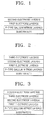
- Fig. 1 is a schematic view showing a structure of a thin film electrode according to an embodiment (first aspect) of the present invention.
- the thin film electrode comprises a first electrode layer 3 and a second electrode layer 4, wherein the electrode layers are laminated in this order on a gallium nitride layer 2 formed on a substrate 1.
- the first electrode layer 3 laminated on top of the p-type gallium nitride layer is an electrode for forming an ohmic contact of a p-type gallium nitride semiconductor.
- a solid solution usable herein includes an element capable of easily breaking Mg-H bonds within the gallium nitride semiconductor, exhibiting an excellent doping effect and forming gallium-related nitrides when annealed. Above all, the solid solution is a material which can form transparent conductive oxides capable of lowering the Schottky barrier when annealed based on an energy bandgap principle between materials and exhibit a high transmittance even in a thickness of 100 ⁇ or more.
- the solid solution in contact with the gallium nitride semiconductor can easily break Mg-H bonds within the gallium nitride semiconductor, exhibit an excellent doping effect or form a number of gallium vacancies around the surface of the gallium nitride layer when annealed at low temperature (800°C or lower), thereby increasing effective carrier concentration around the surface of the gallium nitride layer.
- the increased effective carrier concentration (> 10 18 cm -3 ) on the surface of the gallium nitride lowers the Schottky barrier present in the interface of the metal electrode in contact with the gallium nitride semiconductor so that a number of carriers (holes) can generate high carrier conductivity through a tunneling effect on the basis of quantum concept.
- Ni-X Ni-based solid solution
- X element contained in nickel (a matrix metal) include group II elements such as magnesium (Mg), beryllium (Be), calcium (Ca), zinc (Zn) , etc., which serve as dopants of the p-type gallium nitride.
- group II elements such as magnesium (Mg), beryllium (Be), calcium (Ca), zinc (Zn) , etc.
- Mg magnesium
- Be beryllium
- Ca calcium
- Zn zinc
- the elements When the elements are added to the nickel (Ni) matrix, they exist in a solubilized form at low temperature range rather than in a compound form.
- the elements act as dopants or form a compound through the reaction with gallium to form a number of gallium vacancies like the nickel matrix metal. Accordingly, it is believed that a high quality ohmic contact having excellent electrical properties can be formed with ease.
- group VI elements e.g., sulfur (S), selenium (Se) and tellurium (Te) can be used. Since the group VI elements also can replace nitrogen (N) of the gallium nitride, they act as dopants and form a gallium compound through the reaction with gallium to form a number of gallium vacancies. Accordingly, it is believed that a high quality ohmic contact having excellent electrical properties can be formed with ease.
- group II and VI elements antimony (Sb) and scandium (Sc) which are capable of forming a compound through the reaction with gallium at low temperature can be used as the X element.
- the second electrode layer 4 is an outermost layer of the thin film electrode, and plays a role in (1) inhibiting a surface degradation occurring during an annealing process for the manufacture of devices such as light emitting diodes and laser diodes, 2 ⁇ facilitating the formation of a gallium-related compound, 3 ⁇ preventing nitrogen from flowing out, 4 ⁇ obtaining excellent stability against oxidation and wire adhesion, and 5 ⁇ maintaining a high transparency.
- Representative examples of materials usable as the second electrode layer 4 satisfying the requirements as described above include 1 ⁇ pure metals, e.g., gold (Au), palladium (Pd), platinum (Pt), rhodium (Rh), rhenium (Re) and ruthenium (Ru), (2) transparent conductive oxides (TCOs), e.g., indium tin oxide (ITO), doped zinc oxide (ZnO) and tin oxide (SnO 2 ) , and 3 ⁇ transparent conductive nitrides, e.g., TiN.
- Au gold
- Pd palladium
- platinum platinum
- Rh rhodium
- Re rhenium
- Ru ruthenium
- TCOs transparent conductive oxides
- ITO indium tin oxide
- ZnO doped zinc oxide
- SnO 2 tin oxide
- 3 ⁇ transparent conductive nitrides e.g., TiN.
- Fig. 2 is a schematic view showing a structure of a thin film electrode according to an embodiment (a second aspect) of the present invention.
- the thin film electrode comprises a first electrode layer 3, a second electrode layer 4 and a third electrode layer 5, wherein the electrode layers are laminated in this order on a gallium nitride layer 2 formed on a substrate 1.
- the first and the second electrode layers shown in Fig. 1 are usable in this embodiment. Accordingly, detailed descriptions of the first and the second electrode layers are intentionally omitted in the following description.
- an inverted structure (flip chip) to general LED structures is provided for the third electrode layer.
- conductive oxides or nitrides having an excellent light transmittance can be selected as materials of the third electrode layer.
- Fig. 3 is a schematic view showing a structure of a thin film electrode according to an embodiment (a third aspect) of the present invention.
- the thin film electrode comprises a first electrode layer 3, a second electrode layer 4, a third electrode layer 5 and a fourth electrode layer 6, wherein the electrode layers are laminated in this order on a gallium nitride layer 2 formed on a substrate 1.
- the first, the second, and the third electrode layers shown in Fig. 2 are usable in this embodiment. Accordingly, detailed descriptions of the first, the second and the third electrode layers are intentionally omitted in the following description.
- an inverted structure (flip chip) to general LED structures is provided for the fourth electrode layer.
- highly reflective materials within the short-wavelength region can be selected as materials of the fourth electrode layer.
- highly reflective materials include at least one element selected from the group consisting of Al, Ag, Rh, etc.
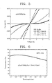
- Fig. 4 is XRD graphs of a nickel-magnesium (Ni-Mg) solid solution used for fabricating a thin film electrode according to an embodiment of the present invention.
- Fig. 4(a) represents the results prior to annealing
- Fig. 4(b) represents the results after annealing at 550°C for 1 minute.
- peaks corresponding to the p-type gallium nitride (GaN) and a sapphire (Al 2 O 3 ) substrate were observed.
- a peak corresponding to the nickel-magnesium (Ni-Mg) solid solution prepared by adding nickel (Ni) to magnesium (Mg) was observed.
- the nickel-magnesium solid solution since the nickel-magnesium solid solution has a strong hydrogen affinity, it breaks Mg-H bonds when contacted with the top of the p-type gallium nitride layer and thus increases the carrier concentration on the surface of the gallium nitride layer.
- the oxidized solid solution is a conductive oxide, and expected to have a large work function compared to nickel oxide (NiO) of a conventional nickel/gold (Ni/Au) structure.
- the oxidized solid solution provides a number of holes to the surface of the gallium nitride and at the same time lowers the Schottky barrier so as to cause exhibition of excellent electrical properties.
- the oxidized nickel-magnesium solid solution plays a central role in enhancing the transparency of the thin metal film.
- Fig. 5 is a graph showing current-voltage characteristic before and after annealing, following depositing a nickel-magnesium (Ni-Mg) solid solution/gold (Au) on a p-type gallium nitride layer having a carrier concentration of 5 x 10 17 in accordance with an embodiment of the present invention.
- Ni-Mg nickel-magnesium
- Au gold
- Fig. 6 is a graph showing results of the transmittance measured after annealing at 550°C for 1 minute, following depositing a nickel-magnesium (Ni-Mg) solid solution/gold (Au) on Corning glass in accordance with an embodiment of the present invention.
- Ni-Mg nickel-magnesium
- Au gold
- the deposited Ni-Mg solid solution/Au showed a transmittance of 80% or more at a wavelength range of 370-450nm.
- Typical metal electrode layers and capping layer deposited for the measurement of transmittance have a thickness of 100 ⁇ or less, while the metal electrode layers and the capping layer used in the present invention have a thickness of about 200 ⁇ . Despite such a large thickness, the electrode layers and capping layer exhibit a transparence of at least 80%.
- the term 'capping layer' used herein refers to an outermost electrode layer.
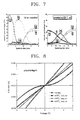
- Fig. 7 is graphs showing the AES (Auger Electron Spectroscopy) depth profile of a nickel-magnesium (Ni-Mg) solid solution used for fabricating a thin film electrode according to a preferred embodiment of the present invention.
- Fig. 7(a) represents the results prior to annealing
- Fig. 7(b) represents the results after annealing at 550°C for 1 minute;
- Fig. 7(a) From Fig. 7(a), it was observed that nickel (Ni) and a small amount of magnesium (Mg) remain on the surface of the gallium nitride layer. Although not shown in Fig. 7(a), the AES data related with magnesium (Mg) reveals that magnesium (Mg) is solubilized in nickel (Ni), rather than is formed into a compound through a reaction with nickel (Ni). Fig. 7(b) apparently shows that the nickel-magnesium solid solution is formed and at the same time an extremely small amount of magnesium is diffused into the surface of gallium nitride and distributed.
- Fig. 8 is a graph showing current-voltage characteristic before and after annealing in air, following depositing a nickel-magnesium (Ni-Mg) solid solution/platinum (Pt) on a p-type gallium nitride layer having a carrier concentration of 5 x 10 17 in accordance with an embodiment of the present invention.
- Ni-Mg nickel-magnesium
- Pt platinum
- a p-type gallium nitride layer having a carrier concentration of 5 x 10 17 in accordance with an embodiment of the present invention.
- Fig. 9 is a graph showing current-voltage characteristics before and after annealing in air, following depositing a nickel-magnesium (Ni-Mg) solid solution/palladium (Pd) on a p-type gallium nitride layer having a carrier concentration of 5 x 10 17 in accordance with an embodiment of the present invention.
- Ni-Mg nickel-magnesium
- Pd palladium
- Fig. 10 is a graph showing current-voltage characteristics before and after annealing in air, following depositing a nickel-magnesium (Ni-Mg) solid solution/ruthenium (Ru) on a p-type gallium nitride layer having a carrier concentration of 5 x 10 17 in accordance with an embodiment of the present invention.
- Ni-Mg nickel-magnesium
- Ru ruthenium
- Fig. 11 is a graph showing current-voltage characteristics before and after annealing in air, following depositing a ruthenium (Ru)/nickel-magnesium (Ni-Mg) solid solution on a p-type gallium nitride layer having a carrier concentration of 5 x 10 17 in accordance with an embodiment of the present invention.
- ruthenium (Ru)/nickel-magnesium (Ni-Mg) solid solution on a p-type gallium nitride layer having a carrier concentration of 5 x 10 17 in accordance with an embodiment of the present invention.
- Fig. 12 is a graph showing current-voltage characteristic before and after annealing in air, following depositing a nickel-zinc (Ni-Zn) solid solution/gold (Au) on a p-type gallium nitride layer having a carrier concentration of 5 x 10 17 in accordance with an embodiment of the present invention.
- Ni-Zn nickel-zinc
- Au gold
- Fig. 13 is a graph showing current-voltage characteristic before and after annealing in air, following depositing a pure nickel (Ni)/nickel-zinc (Ni-Zn) solid solution/gold (Au) on a p-type gallium nitride layer having a carrier concentration of 5 x 10 17 in accordance with an embodiment of the present invention.
- Fig. 14 is a graph showing current-voltage characteristic before and after annealing in air, following depositing a nickel-zinc (Ni-Zn) solid solution/nickel (Ni)/gold (Au) on a p-type gallium nitride layer having a carrier concentration of 5 x 10 17 in accordance with an embodiment of the present invention.
- Ni-Zn nickel-zinc
- Ni nickel-zinc
- Au gold
- a p-type gallium nitride (GaN) layer was placed in an ultrasonic bath, and then washed at 60°C for 5 minutes using trichloroethylene, acetone, methanol and distilled water, respectively.
- the washed p-type gallium nitride layer was subjected to a hard baking process at 100°C for 10 minutes to completely remove moisture remaining on the p-type gallium nitride layer.
- a Photoresist was spin-coated at 4,000rpm onto the p-type gallium nitride layer, and then subjected to a soft baking process at 88°C for 10 minutes.
- a mask was aligned with the GaN layer and exposed to a UV light at an intensity of 22.8mW for 10 seconds, the resulting structure was dipped in a mixture of a developing agent and distilled water (1:4), and developed for 15 seconds.
- the developed sample was dipped in BOE solution for 5 minutes to remove contaminants remaining on the sample.
- a nickel-magnesium (Ni-Mg) solid solution/gold (Au) was deposited on the developed sample in a thickness of 100 ⁇ using an electron-beam evaporator, and then subjected to a lift-off process using acetone.
- the resulting structure was charged into a rapid thermal annealing (RTA) furnace and annealed under air or nitrogen gas at 350 ⁇ 550°C for 1 minute to fabricate a high-grade thin film electrode for forming an ohmic contact.
- RTA rapid thermal annealing
- a procedure was performed in the same manner as in Example 1 up to the step of depositing a Ni-Mg solid solution. Thereafter, platinum (Pt) was deposited using an electron-beam evaporator to form a capping layer in a thickness of 100 ⁇ , and then subjected to a lift-off process using acetone. The resulting structure was charged into a rapid thermal annealing (RTA) furnace and annealed in air at 450 ⁇ 650°C for 1 minute to fabricate a thin metal film for forming an ohmic contact.
- RTA rapid thermal annealing
- a procedure was performed in the same manner as in Example 1 up to the step of depositing a Ni-Mg solid solution. Thereafter, palladium (Pd) was deposited using an electron-beam evaporator to form a capping layer in a thickness of 100 ⁇ , and then subjected to a lift-off process using acetone. The resulting structure was charged into a rapid thermal annealing (RTA) furnace and annealed in air at 450°C for 1 minute to fabricate a thin metal film for forming an ohmic contact.
- RTA rapid thermal annealing
- a procedure was performed in the same manner as in Example 1 up to the step of depositing an electrode layer on a gallium nitride layer. Thereafter, ruthenium (Ru), a nickel-magnesium (Ni-Mg) solid solution and gold (Au) were sequentially deposited in thicknesses of 50 ⁇ and 50 ⁇ , respectively, using an electron-beam evaporator and then subjected to a lift-off process using acetone. The resulting structure was charged into a rapid thermal annealing (RTA) furnace and annealed in air at 350 ⁇ 650°C for 1 minute to fabricate a thin metal film for forming an ohmic contact.
- RTA rapid thermal annealing
- a procedure was performed in the same manner as in Example 1 up to the step of depositing a Ni-Mg solid solution in a thickness of 50 ⁇ . Thereafter, ruthenium (Ru) was deposited using an electron-beam evaporator to form a capping layer in a thickness of 50 ⁇ , and then subjected to a lift-off process using acetone. The resulting structure was charged into a rapid thermal annealing (RTA) furnace and annealed in air at 450°C for 1 minute to fabricate a thin metal film for forming an ohmic contact.
- RTA rapid thermal annealing
- a procedure was performed in the same manner as in Example 1 up to the step of depositing a Ni-Zn solid solution in a thickness of 50 ⁇ . Thereafter, gold (Au) was deposited using an electron-beam evaporator to form a capping layer in a thickness of 50 ⁇ , and then subjected to a lift-off process using acetone. The resulting structure was charged into a rapid thermal annealing (RTA) furnace and annealed in air at 350 ⁇ 650°C for 1 minute to fabricate a thin metal film for forming an ohmic contact.
- RTA rapid thermal annealing
- a procedure was performed in the same manner as in Example 1 up to the step of depositing a Ni-Zn solid solution in a thickness of 30 ⁇ . Thereafter, nickel (Ni) and gold (Au) were deposited in thicknesses of 20 ⁇ and 50 ⁇ , respectively, using an electron-beam evaporator, and then subjected to a lift-off process using acetone. The resulting structure was charged into a rapid thermal annealing (RTA) furnace and annealed in air at 350 ⁇ 650°C for 1 minute to fabricate a thin metal film for forming an ohmic contact.
- RTA rapid thermal annealing
- a procedure was performed in the same manner as in Example 1 up to the step of depositing an electrode layer on a gallium nitride layer. Thereafter, nickel-(Ni), a nickel-zinc (Ni-Zn) solid solution and gold (Au) were sequentially deposited in thicknesses of 20 ⁇ , 30 ⁇ and 50 ⁇ , respectively, using an electron-beam evaporator and then subjected to a lift-off process using acetone. The resulting structure was charged into a rapid thermal annealing (RTA) furnace and annealed in air at 350 ⁇ 650°C for 1 minute to fabricate a thin metal film for forming an ohmic contact.
- RTA rapid thermal annealing
- the thin film electrode for forming an ohmic contact of the present invention is expected to exhibit excellent electrical and optical properties such as low specific contact resistance, excellent current-voltage characteristics, good surface state and high transparence, in particular improved current injection and spreading capabilities. Accordingly, since the thin film electrode for forming an ohmic contact of the present invention can considerably improve electrical and optical efficiencies of gallium nitride light emitting diodes (LEDs) and laser diodes (LDs), it can be utilized in the development of light emitting diodes and laser diodes with high quality in the near future.
- LEDs gallium nitride light emitting diodes
- LDs laser diodes
Abstract
Description
- The present invention relates to a technique for forming a high quality ohmic contact with improved current injection and spreading capabilities, as well as low ohmic contact resistance and high transmittance. The technique for forming a high quality ohmic contact is one of the key techniques for the fabrication of short-wavelength light emitting diodes (LEDs) emitting blue and green visible light and ultraviolet light, and laser diodes (LDs) using a gallium nitride (GaN) semiconductor.
- The formation of a high quality ohmic contact between a semiconductor and an electrode is very important to manufacture photo-related devices using a gallium nitride semiconductor such as light emitting diodes and laser diodes.
- Hitherto, in the case of p-type gallium nitride, thin film electrodes based on nickel (Ni), e.g., a thin metal film of nickel/gold (Ni/Au), have been widely used as thin film electrode structures for ohmic contact. Recently, a variety of metal systems for ohmic contact such as Ni/Pt/Au, Pt/Ni/Au, Pd/Au, etc., are being developed.
- However, there are some problems in the formation of a high quality ohmic contact using p-type gallium nitride. Among these problems, hydrogen atoms (H) of ammonia (NH3), which is an atmospheric gas used for growing p-type gallium nitride, bind with magnesium (Mg) as a p-type dopant to form a Mg-H complex exhibiting electric insulating properties, thereby exhibiting a low effective carrier concentration and a high surface resistance. Accordingly, the formation of a high quality ohmic contact is difficult. Moreover, a low carrier (hole) injection makes the manufacture of high grade optical devices difficult.
- One example for increasing the doping concentration of p-type gallium nitride is disclosed in Japanese Patent Laid-open No. 2001-35796. According to this publication, gallium nitride having an increased carrier concentration is obtained by bring a metal, e.g., zirconium (Zr), having a high hydrogen affinity into contact with the gallium nitride, followed by activating a p-type dopant present in a crystal of the gallium nitride through annealing. As another example, nickel, gold-zinc alloy and gold (Ni/Au-Zn/Au) are sequentially deposited on a gallium nitride layer to form an ohmic contact.
- Another problem is that no high quality ohmic contact systems having a high transmittance in the short-wavelength region have been developed. A nickel/gold (Ni/Au) system currently employed in the LED process has a very thin thickness (< ~100Å) and a transmittance of 80% or more. The ohmic contact using such a thin metal layer can achieve high transmittance, but it is difficult to obtain a sufficient current injection and spreading capabilities, causing low efficiency of optical devices.
- According to the invention there is provided a thin film electrode for forming an ohmic contact in light emitting diodes or laser diodes which comprises a first electrode layer laminated on a p-type gallium nitride layer and including a Ni-X solid solution, and a second electrode layer laminated on the first electrode and including at least one element selected from the group consisting of Au, Pt, Pd, Ni, Ru, Rh, Re, C, Cu and Ir.
- The thin film electrode of the present invention may further comprise a third electrode layer laminated on the second electrode layer and including at least one element selected from the group consisting of Al, Ag and Rh.
- Alternatively, the third electrode layer laminated on the second electrode layer may include at least one compound selected from the group consisting of transparent conductive oxides and transparent conductive nitrides.
- The thin film electrode of the present invention may further comprise a fourth electrode layer laminated on the third electrode layer and including at least one element selected from the group consisting of Al, Ag and Rh.
- In accordance with one aspect of the present invention, there is provided a thin film electrode for forming an ohmic contact in light emitting diodes or laser diodes which comprises a first electrode layer laminated on a p-type gallium nitride layer and including at least one element selected from the group consisting of Au, Pt, Pd, Ni, Ru, Rh, Re, C, Cu and Ir, and a second electrode layer laminated on the first electrode and including a Ni-X solid solution.
- The thin film electrode of the present invention may further comprise a third electrode layer laminated on the second electrode layer and including at least one element selected from the group consisting of Al, Ag and Rh.
- Alternatively, the thin film electrode of the present invention may further comprise a third electrode layer laminated on the second electrode layer and including at least one compound selected from the group consisting of transparent conductive oxides and transparent conductive nitrides, and a fourth electrode layer laminated on the third electrode layer and including at least one element selected from the group consisting of Al, Ag and Rh.
- In accordance with another aspect of the present invention, there is provided a thin film electrode for forming an ohmic contact in light emitting diodes or laser diodes which comprises a first electrode layer laminated on a p-type gallium nitride layer and including a Ni-X solid solution, and a second electrode layer laminated on the first electrode and including at least one compound selected from the group consisting of transparent conductive oxides and transparent conductive nitrides.
- The thin film electrode of the present invention may further comprise a third electrode layer laminated on the second electrode layer and including at least one element selected from the group consisting of Al, Ag and Rh.
- In accordance with another aspect of the present invention, there is provided a thin film electrode for forming an ohmic contact in light emitting diodes or laser diodes which comprises a first electrode layer laminated on a p-type gallium nitride layer and including a Ni-X solid solution, and a second electrode layer laminated on the first electrode and including at least one element selected from the group consisting of Al, Ag and Rh.
- The Ni-based (Ni-X) solid solution used in the present invention includes nickel (Ni) as a matrix metal, and X including at least one element selected from the group consisting of group II elements, group VI elements, Sc, Y, Ge, Sn and Sb.
- The group II elements include one element selected from the group consisting of Mg, Be, Ca and Zn.
- The group VI elements include one element selected from the group consisting of S, Se and Te.
- The X element constituting the Ni-based (Ni-X) solid solution is added in the amount of 1-49 atomic percentage (%).
- The thickness of the electrode layer formed from the Ni-based solid solution is within the range of 1~1, 000Å. The overall thickness of the first, the second, the third, and the fourth electrode layers is within the range of 1~50, 000Å.
- The p-type gallium nitride used in the present invention preferably has a composition of AlxInyGazN (where 0 < x < 1, 0 < y < 1, 0 < z < 1, and x + y + z = 1) .
- In accordance with yet another aspect of the present invention there is provided a method for fabricating the thin film electrodes on the p-type gallium nitride layer, comprising the steps of:
- washing carbon and oxygen layers formed on a gallium nitride semiconductor to remove impurities therefrom;
- depositing a nickel-based solid solution under a high vacuum of 2 x 10⁻⁶ ~ 5 x 10⁻⁸ torr using an electron beam evaporation, an electron ray evaporaion, a sputtering, a plasma laser deposition or an electrochemical process; and
- annealing the deposited nickel-based solid solution under air, oxygen or nitrogen atmosphere at 250~800°C for 30 seconds - 1 hour.
-
- The present inventors have conducted intensive research to realize a high-grade ohmic contact system. As a result, the present inventors have found that when a nickel (Ni)-based solid solution is deposited on top of a p-type gallium nitride semiconductor and then annealed near the melting point of a solubilized metal element such as magnesium (Mg) or zinc (Zn), an excellent doping effect of magnesium (Mg) and zinc (Zn) on the surface of the gallium nitride layer can be obtained, effective carrier concentration around the surface of the gallium nitride layer can be increased by the formation of a number of gallium vacancies due to reaction with gallium, or an energy band between the gallium nitride and deposited oxidized material can be controlled. These improvements allow the high-grade ohmic contact system to exhibit an excellent current-voltage characteristic and a low specific contact resistance, as well as a high transmittance in the short-wavelength region.
- In addition, the present inventors tried to accomplish the following five technical objects. As a result, the present inventors realized the formation of a high-grade ohmic contact based on a new concept using a Ni-X solid solution, which is different from previously developed techniques. The technical objects performed by the present inventors are as follows:
- 1 ○ Increased effective carrier concentration on the surface of gallium nitride: Mg-H bonds are broken using the excellent hydrogen affinity of the Ni-X solid solution;
- 2 ○ High light transmittance in the short-wavelength
region and large work function: a small amount of an X element
is added to nickel oxide (NiO) to form a Ni-X oxide (NixAyO)
[A. Azens et al., Thin Solid Films 422, 2002, 1]; - 3 ○ Excellent doping effect: the X element solubilized in
the Ni-X solid solution is annealed.
[M. H. G. Jacobs, P. J. Spencer, J. Chem. Phys. 90, 1993, 167] ; - 4 ○ Creation of a number of gallium vacancies: Ni as a matrix metal or the X element and gallium (Ga) are reacted to form a compound.
- 5 ○ Formation of a high-grade ohmic contact based on an energy bandgap principle: a deposited Ni-based solid solution is annealed to form an oxide, which is advantageous in terms of easy formation of an ohmic contact of p-type gallium nitride.
-
- The present inventors have found that when a Ni-Mg solid solution as a Ni-X solid solution is ohmic-contacted with p-type gallium nitride, superior results can be obtained compared to those reported so far, and accomplished the present invention.
- Therefore, the object of the present invention is to provide an ohmic contact metal system with excellent electrical, optical, thermal and structural properties which exhibits an increased effective carrier concentration (1 ○, 3 ○ and 4 ○), a reduced Schottky barrier through a controlled energy bandgap between materials (5 ○) and a high transmittance (2 ○).
- The above and other objects, features and other advantages of the present invention will be more clearly understood from the following detailed description taken in conjunction with the accompanying drawings, in which:
- Fig. 1 is a schematic view showing a structure of a thin film electrode according to an embodiment (a first aspect) of the present invention;
- Fig. 2 is a schematic view showing a structure of a thin film electrode according to an embodiment (a second aspect) of the present invention;
- Fig. 3 is a schematic view showing a structure of a thin film electrode according to an embodiment (a third aspect) of the present invention;
- Fig. 4 is XRD graphs of a nickel-magnesium (Ni-Mg) solid solution used for fabricating a thin film electrode according to an embodiment of the present invention. Fig. 4(a) represents the results prior to annealing and Fig. 4(b) represents the results after annealing at 550°C for 1 minute;
- Fig. 5 is a graph showing current-voltage characteristics before and after annealing, following depositing a nickel-magnesium (Ni-Mg) solid solution/gold (Au) on a p-type gallium nitride layer having a carrier concentration of 5 x 10¹⁷ in accordance with an embodiment of the present invention;
- Fig. 6 is a graph showing results of the transmittance measured after annealing, following depositing a nickel-magnesium (Ni-Mg) solid solution/gold (Au) on a Corning glass in accordance with an embodiment of the present invention;
- Fig. 7 is graphs showing the AES (Atomic Emission Spectrometer) depth profiles of a nickel-magnesium (Ni-Mg) solid solution used for fabricating a thin film electrode according to a preferred embodiment of the present invention. Fig. 7(a) represents the results prior to annealing, and Fig. 7(b) represents the results after annealing at 550°C for 1 minute;
- Fig. 8 is a graph showing current-voltage characteristic before and after annealing, following depositing a nickel-magnesium (Ni-Mg) solid solution/platinum (Pt) on a p-type gallium nitride layer having a carrier concentration of 5 x 10¹⁷ in accordance with an embodiment of the present invention;
- Fig. 9 is a graph showing current-voltage characteristics before and after annealing, following depositing a nickel-magnesium (Ni-Mg) solid solution/palladium (Pd) on a p-type gallium nitride layer having a carrier concentration of 5 x 10¹⁷ in accordance with an embodiment of the present invention;
- Fig. 10 is a graph showing current-voltage characteristics before and after annealing in air, following depositing a nickel-magnesium (Ni-Mg) solid solution/ruthenium (Ru) on a p-type gallium nitride layer having a carrier concentration of 5 x 10¹⁷;
- Fig. 11 is a graph showing current-voltage characteristics before and after annealing in air, following depositing a ruthenium (Ru)/nickel-magnesium (Ni-Mg) solid solution on a p-type gallium nitride layer having a carrier concentration of 5 x 10¹⁷;
- Fig. 12 is a graph showing current-voltage characteristics before and after annealing in air, following depositing a nickel-zinc (Ni-Zn) solid solution/gold (Au) on a p-type gallium nitride layer having a carrier concentration of 5 x 10¹⁷;
- Fig. 13 is a graph showing current-voltage characteristics before and after annealing in air, following depositing a pure nickel (Ni)/nickel-zinc (Ni-Zn) solid solution/gold (Au) on a p-type gallium nitride layer having a carrier concentration of 5 x 10¹⁷ ; and
- Fig. 14 is a graph showing current-voltage characteristics before and after annealing in air, following depositing a nickel-zinc (Ni-Zn) solid solution/nickel (Ni)/gold (Au) on a p-type gallium nitride layer having a carrier concentration of 5 x 10¹⁷.
-
- Hereinafter, the present invention will be explained in more detail with reference to the accompanying drawings.
- Fig. 1 is a schematic view showing a structure of a thin film electrode according to an embodiment (first aspect) of the present invention.
- Referring to Fig. 1, the thin film electrode comprises a
first electrode layer 3 and asecond electrode layer 4, wherein the electrode layers are laminated in this order on agallium nitride layer 2 formed on asubstrate 1. - Referring to Fig. 1, the
first electrode layer 3 laminated on top of the p-type gallium nitride layer is an electrode for forming an ohmic contact of a p-type gallium nitride semiconductor. A solid solution usable herein includes an element capable of easily breaking Mg-H bonds within the gallium nitride semiconductor, exhibiting an excellent doping effect and forming gallium-related nitrides when annealed. Above all, the solid solution is a material which can form transparent conductive oxides capable of lowering the Schottky barrier when annealed based on an energy bandgap principle between materials and exhibit a high transmittance even in a thickness of 100Å or more. - The solid solution in contact with the gallium nitride semiconductor can easily break Mg-H bonds within the gallium nitride semiconductor, exhibit an excellent doping effect or form a number of gallium vacancies around the surface of the gallium nitride layer when annealed at low temperature (800°C or lower), thereby increasing effective carrier concentration around the surface of the gallium nitride layer.
- The increased effective carrier concentration (> 1018cm-3) on the surface of the gallium nitride lowers the Schottky barrier present in the interface of the metal electrode in contact with the gallium nitride semiconductor so that a number of carriers (holes) can generate high carrier conductivity through a tunneling effect on the basis of quantum concept.
- A representative example of the solid solution satisfying the requirements as discussed above is a Ni-based solid solution (Ni-X) which exhibits a strong hydrogen affinity. Examples of the X element contained in nickel (a matrix metal) include group II elements such as magnesium (Mg), beryllium (Be), calcium (Ca), zinc (Zn) , etc., which serve as dopants of the p-type gallium nitride. When the elements are added to the nickel (Ni) matrix, they exist in a solubilized form at low temperature range rather than in a compound form. When annealed around a melting temperature of the elements following the deposition, the elements act as dopants or form a compound through the reaction with gallium to form a number of gallium vacancies like the nickel matrix metal. Accordingly, it is believed that a high quality ohmic contact having excellent electrical properties can be formed with ease.
- As the X element added to the nickel (Ni) matrix metal, group VI elements, e.g., sulfur (S), selenium (Se) and tellurium (Te) can be used. Since the group VI elements also can replace nitrogen (N) of the gallium nitride, they act as dopants and form a gallium compound through the reaction with gallium to form a number of gallium vacancies. Accordingly, it is believed that a high quality ohmic contact having excellent electrical properties can be formed with ease. In addition to the group II and VI elements, antimony (Sb) and scandium (Sc) which are capable of forming a compound through the reaction with gallium at low temperature can be used as the X element.
- The
second electrode layer 4 is an outermost layer of the thin film electrode, and plays a role in (1) inhibiting a surface degradation occurring during an annealing process for the manufacture of devices such as light emitting diodes and laser diodes, 2 ○ facilitating the formation of a gallium-related compound, 3 ○ preventing nitrogen from flowing out, 4 ○ obtaining excellent stability against oxidation and wire adhesion, and 5 ○ maintaining a high transparency. - Representative examples of materials usable as the
second electrode layer 4 satisfying the requirements as described above include 1 ○ pure metals, e.g., gold (Au), palladium (Pd), platinum (Pt), rhodium (Rh), rhenium (Re) and ruthenium (Ru), (2) transparent conductive oxides (TCOs), e.g., indium tin oxide (ITO), doped zinc oxide (ZnO) and tin oxide (SnO2) , and 3 ○ transparent conductive nitrides, e.g., TiN. - Fig. 2 is a schematic view showing a structure of a thin film electrode according to an embodiment (a second aspect) of the present invention.
- Referring to Fig. 2, the thin film electrode comprises a
first electrode layer 3, asecond electrode layer 4 and athird electrode layer 5, wherein the electrode layers are laminated in this order on agallium nitride layer 2 formed on asubstrate 1. - The first and the second electrode layers shown in Fig. 1 are usable in this embodiment. Accordingly, detailed descriptions of the first and the second electrode layers are intentionally omitted in the following description.
- In particular, in order to maximize the light emitting efficiency of light emitting diodes (LEDs), an inverted structure (flip chip) to general LED structures is provided for the third electrode layer. To this end, conductive oxides or nitrides having an excellent light transmittance can be selected as materials of the third electrode layer.
- Fig. 3 is a schematic view showing a structure of a thin film electrode according to an embodiment (a third aspect) of the present invention. Referring to Fig. 3, the thin film electrode comprises a
first electrode layer 3, asecond electrode layer 4, athird electrode layer 5 and afourth electrode layer 6, wherein the electrode layers are laminated in this order on agallium nitride layer 2 formed on asubstrate 1. - The first, the second, and the third electrode layers shown in Fig. 2 are usable in this embodiment. Accordingly, detailed descriptions of the first, the second and the third electrode layers are intentionally omitted in the following description.
- In particular, in order to maximize the light emitting efficiency of light emitting diodes (LEDs), an inverted structure (flip chip) to general LED structures is provided for the fourth electrode layer. To this end, highly reflective materials within the short-wavelength region can be selected as materials of the fourth electrode layer. At this time, highly reflective materials include at least one element selected from the group consisting of Al, Ag, Rh, etc.
- Fig. 4 is XRD graphs of a nickel-magnesium (Ni-Mg) solid solution used for fabricating a thin film electrode according to an embodiment of the present invention. Fig. 4(a) represents the results prior to annealing, and Fig. 4(b) represents the results after annealing at 550°C for 1 minute.
- From the graph of Fig. 4(a), peaks corresponding to the p-type gallium nitride (GaN) and a sapphire (Al2O3) substrate were observed. In addition, a peak corresponding to the nickel-magnesium (Ni-Mg) solid solution prepared by adding nickel (Ni) to magnesium (Mg) was observed.
- That is, since the nickel-magnesium solid solution has a strong hydrogen affinity, it breaks Mg-H bonds when contacted with the top of the p-type gallium nitride layer and thus increases the carrier concentration on the surface of the gallium nitride layer.
- From Fig. 4(b), in addition to a peak corresponding to the p-type gallium nitride (GaN), peaks corresponding to an oxidized Ni-Mg-O solid solution (Ni1-xMgxO) , which is an oxidized state of the Ni-Mg solid solution prior to annealing, and NiGa as a nickel-gallium compound, were observed.
- In particular, the oxidized solid solution is a conductive oxide, and expected to have a large work function compared to nickel oxide (NiO) of a conventional nickel/gold (Ni/Au) structure. In addition, the oxidized solid solution provides a number of holes to the surface of the gallium nitride and at the same time lowers the Schottky barrier so as to cause exhibition of excellent electrical properties. Furthermore, it can be inferred that the oxidized nickel-magnesium solid solution plays a central role in enhancing the transparency of the thin metal film.
- Fig. 5 is a graph showing current-voltage characteristic before and after annealing, following depositing a nickel-magnesium (Ni-Mg) solid solution/gold (Au) on a p-type gallium nitride layer having a carrier concentration of 5 x 10¹⁷ in accordance with an embodiment of the present invention.
- Current-voltage characteristics were measured after annealing at temperatures of 450°C and 550°C in air for 1 minute, respectively. The current-voltage measurement showed a specific contact resistance of 8.45 x 10⁻⁶ cm2 and 6.08 x 10⁻⁶ cm2 at each temperature. The graph obtained in air shows a linear curve which distinctly indicates a good ohmic contact, while the graph obtained under nitrogen shows a non-linear curve which shows a rectifying contact.
- Fig. 6 is a graph showing results of the transmittance measured after annealing at 550°C for 1 minute, following depositing a nickel-magnesium (Ni-Mg) solid solution/gold (Au) on Corning glass in accordance with an embodiment of the present invention.
- The deposited Ni-Mg solid solution/Au showed a transmittance of 80% or more at a wavelength range of 370-450nm. Typical metal electrode layers and capping layer deposited for the measurement of transmittance have a thickness of 100Å or less, while the metal electrode layers and the capping layer used in the present invention have a thickness of about 200Å. Despite such a large thickness, the electrode layers and capping layer exhibit a transparence of at least 80%. The term 'capping layer' used herein refers to an outermost electrode layer.
- Fig. 7 is graphs showing the AES (Auger Electron Spectroscopy) depth profile of a nickel-magnesium (Ni-Mg) solid solution used for fabricating a thin film electrode according to a preferred embodiment of the present invention. Fig. 7(a) represents the results prior to annealing, and Fig. 7(b) represents the results after annealing at 550°C for 1 minute;
- From Fig. 7(a), it was observed that nickel (Ni) and a small amount of magnesium (Mg) remain on the surface of the gallium nitride layer. Although not shown in Fig. 7(a), the AES data related with magnesium (Mg) reveals that magnesium (Mg) is solubilized in nickel (Ni), rather than is formed into a compound through a reaction with nickel (Ni). Fig. 7(b) apparently shows that the nickel-magnesium solid solution is formed and at the same time an extremely small amount of magnesium is diffused into the surface of gallium nitride and distributed.
- Fig. 8 is a graph showing current-voltage characteristic before and after annealing in air, following depositing a nickel-magnesium (Ni-Mg) solid solution/platinum (Pt) on a p-type gallium nitride layer having a carrier concentration of 5 x 10¹⁷ in accordance with an embodiment of the present invention.
- After the deposited Ni-Mg solid solution/Pt was annealed at 450~650°C for 1 minute, current-voltage characteristics were measured. As a result, a distinctly linear curve was obtained. The linear curve indicates that the ohmic contact resistance obtained at a level of 10-5~10-6cm2 represents a good ohmic contact.
- Fig. 9 is a graph showing current-voltage characteristics before and after annealing in air, following depositing a nickel-magnesium (Ni-Mg) solid solution/palladium (Pd) on a p-type gallium nitride layer having a carrier concentration of 5 x 10¹⁷ in accordance with an embodiment of the present invention.
- After the deposited Ni-Mg solid solution/Pd was annealed at 450°C for 1 minute, current-voltage characteristics were measured. As a result, a distinctly linear curve was obtained. The linear curve indicates that the ohmic contact resistance obtained at a level of 10-5cm2 represents a good ohmic contact.
- Fig. 10 is a graph showing current-voltage characteristics before and after annealing in air, following depositing a nickel-magnesium (Ni-Mg) solid solution/ruthenium (Ru) on a p-type gallium nitride layer having a carrier concentration of 5 x 10¹⁷ in accordance with an embodiment of the present invention.
- Fig. 11 is a graph showing current-voltage characteristics before and after annealing in air, following depositing a ruthenium (Ru)/nickel-magnesium (Ni-Mg) solid solution on a p-type gallium nitride layer having a carrier concentration of 5 x 10¹⁷ in accordance with an embodiment of the present invention.
- There is a need to compare the results shown in Figs. 11 and 12 with conventional ohmic structures of nickel/ruthenium (Ni/Ru) and ruthenium/nickel (Ru/Ni). In particular, when annealed at 550°C for 1 minute, the current-voltage characteristics of the nickel/ruthenium (Ni/Ru) ohmic structure was identified to be difficult structures to form an ohmic contact. From the graphs of Figs. 11 and 12, linear curves showing that the ohmic contact resistance obtained at a level of 10-5cm2 represents a good ohmic contact were obtained by the addition of magnesium.
- Fig. 12 is a graph showing current-voltage characteristic before and after annealing in air, following depositing a nickel-zinc (Ni-Zn) solid solution/gold (Au) on a p-type gallium nitride layer having a carrier concentration of 5 x 10¹⁷ in accordance with an embodiment of the present invention.
- After the deposited nickel-zinc (Ni-Zn) solid solution/gold (Au) was annealed at 500°C for 1 minute, current-voltage characteristics were measured. As a result, a distinctly linear curve was obtained. The linear curve indicates that the ohmic contact resistance obtained at a level of 10-5 cm2 represents a good ohmic contact.
- Fig. 13 is a graph showing current-voltage characteristic before and after annealing in air, following depositing a pure nickel (Ni)/nickel-zinc (Ni-Zn) solid solution/gold (Au) on a p-type gallium nitride layer having a carrier concentration of 5 x 10¹⁷ in accordance with an embodiment of the present invention.
- After the deposited pure nickel (Ni)/nickel-zinc (Ni-Zn) solid solution/gold (Au) was annealed at 500°C for 1 minute, current-voltage characteristic was measured. As a result, a distinctly linear curve was obtained. The linear curve indicates that the ohmic contact resistance obtained at a level of 10-6cm2 represents a good ohmic contact.
- Fig. 14 is a graph showing current-voltage characteristic before and after annealing in air, following depositing a nickel-zinc (Ni-Zn) solid solution/nickel (Ni)/gold (Au) on a p-type gallium nitride layer having a carrier concentration of 5 x 10¹⁷ in accordance with an embodiment of the present invention.
- After the deposited nickel-zinc (Ni-Zn) solid solution/nickel (Ni)/gold (Au) was annealed at 500°C for 1 minute, current-voltage characteristics were measured. As a result, a distinctly linear curve was obtained. The linear curve indicates that the ohmic contact resistance obtained at a level of 10-6cm2 represents a good ohmic contact.
- Hereinafter, the present invention will be described in more detail with reference to the following Examples. However, these Examples are given for the purpose of illustration and are not to be construed as limiting the scope of the invention.
- A p-type gallium nitride (GaN) layer was placed in an ultrasonic bath, and then washed at 60°C for 5 minutes using trichloroethylene, acetone, methanol and distilled water, respectively. The washed p-type gallium nitride layer was subjected to a hard baking process at 100°C for 10 minutes to completely remove moisture remaining on the p-type gallium nitride layer. A Photoresist was spin-coated at 4,000rpm onto the p-type gallium nitride layer, and then subjected to a soft baking process at 88°C for 10 minutes. In order to develop a mask pattern on the p-type gallium nitride layer, a mask was aligned with the GaN layer and exposed to a UV light at an intensity of 22.8mW for 10 seconds, the resulting structure was dipped in a mixture of a developing agent and distilled water (1:4), and developed for 15 seconds.
- Thereafter, the developed sample was dipped in BOE solution for 5 minutes to remove contaminants remaining on the sample. A nickel-magnesium (Ni-Mg) solid solution/gold (Au) was deposited on the developed sample in a thickness of 100Å using an electron-beam evaporator, and then subjected to a lift-off process using acetone. The resulting structure was charged into a rapid thermal annealing (RTA) furnace and annealed under air or nitrogen gas at 350~550°C for 1 minute to fabricate a high-grade thin film electrode for forming an ohmic contact.
- A procedure was performed in the same manner as in Example 1 up to the step of depositing a Ni-Mg solid solution. Thereafter, platinum (Pt) was deposited using an electron-beam evaporator to form a capping layer in a thickness of 100Å, and then subjected to a lift-off process using acetone. The resulting structure was charged into a rapid thermal annealing (RTA) furnace and annealed in air at 450~650°C for 1 minute to fabricate a thin metal film for forming an ohmic contact.
- A procedure was performed in the same manner as in Example 1 up to the step of depositing a Ni-Mg solid solution. Thereafter, palladium (Pd) was deposited using an electron-beam evaporator to form a capping layer in a thickness of 100Å, and then subjected to a lift-off process using acetone. The resulting structure was charged into a rapid thermal annealing (RTA) furnace and annealed in air at 450°C for 1 minute to fabricate a thin metal film for forming an ohmic contact.
- A procedure was performed in the same manner as in Example 1 up to the step of depositing an electrode layer on a gallium nitride layer. Thereafter, ruthenium (Ru), a nickel-magnesium (Ni-Mg) solid solution and gold (Au) were sequentially deposited in thicknesses of 50Å and 50Å, respectively, using an electron-beam evaporator and then subjected to a lift-off process using acetone. The resulting structure was charged into a rapid thermal annealing (RTA) furnace and annealed in air at 350~650°C for 1 minute to fabricate a thin metal film for forming an ohmic contact.
- A procedure was performed in the same manner as in Example 1 up to the step of depositing a Ni-Mg solid solution in a thickness of 50Å. Thereafter, ruthenium (Ru) was deposited using an electron-beam evaporator to form a capping layer in a thickness of 50Å, and then subjected to a lift-off process using acetone. The resulting structure was charged into a rapid thermal annealing (RTA) furnace and annealed in air at 450°C for 1 minute to fabricate a thin metal film for forming an ohmic contact.
- A procedure was performed in the same manner as in Example 1 up to the step of depositing a Ni-Zn solid solution in a thickness of 50Å. Thereafter, gold (Au) was deposited using an electron-beam evaporator to form a capping layer in a thickness of 50Å, and then subjected to a lift-off process using acetone. The resulting structure was charged into a rapid thermal annealing (RTA) furnace and annealed in air at 350~650°C for 1 minute to fabricate a thin metal film for forming an ohmic contact.
- A procedure was performed in the same manner as in Example 1 up to the step of depositing a Ni-Zn solid solution in a thickness of 30Å. Thereafter, nickel (Ni) and gold (Au) were deposited in thicknesses of 20Å and 50Å, respectively, using an electron-beam evaporator, and then subjected to a lift-off process using acetone. The resulting structure was charged into a rapid thermal annealing (RTA) furnace and annealed in air at 350~650°C for 1 minute to fabricate a thin metal film for forming an ohmic contact.
- A procedure was performed in the same manner as in Example 1 up to the step of depositing an electrode layer on a gallium nitride layer. Thereafter, nickel-(Ni), a nickel-zinc (Ni-Zn) solid solution and gold (Au) were sequentially deposited in thicknesses of 20Å, 30Å and 50Å, respectively, using an electron-beam evaporator and then subjected to a lift-off process using acetone. The resulting structure was charged into a rapid thermal annealing (RTA) furnace and annealed in air at 350~650°C for 1 minute to fabricate a thin metal film for forming an ohmic contact.
- As apparent from the above description, when a nickel (Ni)-based solid solution to be used as a metal electrode layer is deposited on a gallium nitride layer and then annealed near the melting point of a solubilized metal element such as magnesium (Mg) or zinc (Zn), an excellent doping effect of magnesium (Mg) and zinc (Zn) on the surface of the gallium nitride layer can be obtained, effective carrier concentration around the surface of the gallium nitride layer can be increased by the formation of a number of gallium vacancies due to reaction with gallium, or an energy band between the gallium nitride and deposited oxidized material can be controlled. These improvements allow the high-grade ohmic contact system of the present invention to exhibit excellent current-voltage characteristics and a low specific contact resistance, as well as a high transmittance in the short-wavelength region.
- In addition, the thin film electrode for forming an ohmic contact of the present invention is expected to exhibit excellent electrical and optical properties such as low specific contact resistance, excellent current-voltage characteristics, good surface state and high transparence, in particular improved current injection and spreading capabilities. Accordingly, since the thin film electrode for forming an ohmic contact of the present invention can considerably improve electrical and optical efficiencies of gallium nitride light emitting diodes (LEDs) and laser diodes (LDs), it can be utilized in the development of light emitting diodes and laser diodes with high quality in the near future.
- Although the preferred embodiments of the present invention have been disclosed for illustrative purposes, those skilled in the art will appreciate that various modifications, additions and substitutions are possible, without departing from the scope and spirit of the invention as disclosed in the accompanying claims.
Claims (15)
- A thin film electrode for forming an ohmic contact in light emitting diodes or laser diodes, comprising:wherein a first one of the first and second electrode layers includes an Ni-X solid solution; anda first electrode layer laminated on a p-type gallium nitride layer; anda second electrode layer laminated on the first electrode;
a second one of the first and second electrode layers includes at least one element selected from the group consisting of Au, Pt, Pd, Ni, Ru, Rh, Re, C, Cu and Ir or at least one compound selected from the group consisting of transparent conductive oxides and transparent conductive nitrides; or Al, Ag or Rh. - A thin-film electrode according to claim 1 wherein the first electrode layer includes a Ni-X solid solution and the second electrode layer includes at least one element selected from the group consisting of Au, Pt, Pd, Ni, Ru, Rh, Re, C, Cu and Ir.
- A thin-film electrode according to claim 1 wherein the second electrode layer includes a Ni-X solid solution and the first electrode layer includes at least one element selected from the group consisting of Au, Pt, Pd, Ni, Ru, Rh, Re, C, Cu and Ir.
- The thin film electrode according to claim 1, 2 or 3, further comprising a third electrode layer laminated on the second electrode layer and including at least one element selected from the group consisting of transparent conductive oxides and transparent conductive nitrides.
- The thin film electrode according to claim 4, further comprising a fourth electrode layer laminated on the third electrode layer and including at least one element selected from the group consisting of Al, Ag and Rh.
- A thin-film electrode according to claim 1 wherein the first electrode layer includes a Ni-X solid solution and the second electrode layer includes at least one compound selected from the group consisting of transparent conductive oxides and transparent conductive nitrides.
- The thin film electrode according to claim 1, 2, 3 or 6, further comprising a third electrode layer laminated on the second electrode layer and including at least one element selected from the group consisting of Al, Ag and Rh.
- A thin film electrode according to claim 1 wherein the first electrode layer includes a Ni-X solid solution and the second electrode layer includes at least one element selected from the group of Al, Ag and Rh.
- The thin film electrode according to any one of claims 1 to 8, wherein the Ni-based (Ni-X) solid solution includes nickel (Ni) as a matrix metal, and X including at least one element selected from the group consisting of group II elements, group VI elements, Sc, Y, Ge, Sn and Sb.
- The thin film electrode according to claim 9, wherein the group II elements include one element selected from the group consisting of Mg, Be, Ca and Zn.
- The thin film electrode according to claim 9, wherein the group VI elements include one element selected from the group consisting of S, Se and Te.
- The thin film electrode according to claim 9, wherein the X element constituting the Ni-based (Ni-X) solid solution is added in the amount of 1-49 atomic percent (%).
- The thin film electrode according to any one of claims 1 to 8, wherein the electrode layers formed from the Ni-based solid solution have a thickness of 1~1, 000Å, and the first, the second, the third, and the fourth electrode layers have an overall thickness of 1~10, 000Å.
- The thin film electrode according to any one of claims 1 to 8, wherein the p-type gallium nitride has a composition of AlxInyGazN (where 0 < x < 1, 0 < y < 1, 0 < z < 1, and x + y + z = 1).
- A method for fabricating a thin film electrode on the p-type gallium nitride layer, comprising the steps of:washing carbon and oxygen layers formed on a gallium nitride semiconductor to remove impurities therefrom;depositing a nickel-based solid solution under a high vacuum of 2 x 10⁻⁶ to 5 x 10⁻⁸ torr using an electron beam evaporation, an electron ray evaporation, a sputtering process, a plasma laser deposition or an electrochemical process; andannealing the deposited nickel-based solid solution under air, oxygen or nitrogen atmosphere at 250~800°C for 30 seconds to 1 hour.
Applications Claiming Priority (2)
| Application Number | Priority Date | Filing Date | Title |
|---|---|---|---|
| KR1020030029073A KR100612832B1 (en) | 2003-05-07 | 2003-05-07 | Metal thin film and the produce method for development of ohmic contact using Ni-based solid solution for high-quality optical devices related to GaN |
| KR2003029073 | 2003-05-07 |
Publications (2)
| Publication Number | Publication Date |
|---|---|
| EP1475845A1 true EP1475845A1 (en) | 2004-11-10 |
| EP1475845B1 EP1475845B1 (en) | 2015-06-10 |
Family
ID=36385331
Family Applications (1)
| Application Number | Title | Priority Date | Filing Date |
|---|---|---|---|
| EP04251791.2A Expired - Lifetime EP1475845B1 (en) | 2003-05-07 | 2004-03-26 | Ohmic contacts using Ni-based solid solution for p-type GaN in LEDs |
Country Status (5)
| Country | Link |
|---|---|
| US (2) | US6989598B2 (en) |
| EP (1) | EP1475845B1 (en) |
| JP (2) | JP4803968B2 (en) |
| KR (1) | KR100612832B1 (en) |
| CN (1) | CN100517774C (en) |
Cited By (3)
| Publication number | Priority date | Publication date | Assignee | Title |
|---|---|---|---|---|
| EP1536481A3 (en) * | 2003-10-27 | 2006-10-18 | Samsung Electronics Co., Ltd. | GaN-based III-V group compound semiconductor device and p-type electrode for the same |
| EP2273573A1 (en) * | 2009-03-11 | 2011-01-12 | Panasonic Corporation | Nitride semiconductor element and method for manufacturing same |
| US8729587B2 (en) | 2010-04-01 | 2014-05-20 | Panasonic Corporation | Nitride semiconductor element and manufacturing method therefor |
Families Citing this family (30)
| Publication number | Priority date | Publication date | Assignee | Title |
|---|---|---|---|---|
| KR100624411B1 (en) * | 2003-08-25 | 2006-09-18 | 삼성전자주식회사 | light emitting device and method of manufacturing the same |
| KR100590532B1 (en) * | 2003-12-22 | 2006-06-15 | 삼성전자주식회사 | Flip-chip light emitting diodes and method of manufacturing thereof |
| CN100401541C (en) * | 2005-01-14 | 2008-07-09 | 财团法人工业技术研究院 | Quantum spot/quantum well light emitting diode |
| US7932111B2 (en) * | 2005-02-23 | 2011-04-26 | Cree, Inc. | Substrate removal process for high light extraction LEDs |
| KR100878433B1 (en) * | 2005-05-18 | 2009-01-13 | 삼성전기주식회사 | Fablication methodes of ohmic contact layer and light emitting device adopting the layer |
| JP5138873B2 (en) * | 2005-05-19 | 2013-02-06 | 日亜化学工業株式会社 | Nitride semiconductor device |
| KR20070035660A (en) * | 2005-09-28 | 2007-04-02 | 엘지이노텍 주식회사 | Fabrication method nitride semiconductor light emitting device |
| WO2007069871A1 (en) | 2005-12-16 | 2007-06-21 | Samsung Electronics Co., Ltd. | Optical device and method of fabricating the same |
| JP5244614B2 (en) * | 2005-12-27 | 2013-07-24 | 三星ディスプレイ株式會社 | Group III nitride light emitting device |
| CN1851941A (en) * | 2006-04-30 | 2006-10-25 | 普光科技(广州)有限公司 | Method for making gallium nitride light-emitting-diode chip |
| JP4884866B2 (en) * | 2006-07-25 | 2012-02-29 | 三菱電機株式会社 | Manufacturing method of nitride semiconductor device |
| KR100845037B1 (en) * | 2006-08-02 | 2008-07-09 | 포항공과대학교 산학협력단 | Ohmic electrode and method thereof, semiconductor light emitting element having this |
| JP5522648B2 (en) * | 2008-04-01 | 2014-06-18 | 独立行政法人産業技術総合研究所 | Bonding protection structure between diamond surface and metal piece |
| WO2010039284A1 (en) | 2008-09-30 | 2010-04-08 | Youngstown State University | Silicon carbide barrier diode |
| WO2010113238A1 (en) * | 2009-04-03 | 2010-10-07 | パナソニック株式会社 | Nitride semiconductor element and method for manufacturing same |
| WO2010113237A1 (en) * | 2009-04-03 | 2010-10-07 | パナソニック株式会社 | Nitride semiconductor element and method for manufacturing same |
| US8488230B2 (en) * | 2009-08-24 | 2013-07-16 | Cavendish Kinetics, Inc. | Fabrication of a floating rocker MEMS device for light modulation |
| CN102214762A (en) * | 2010-04-06 | 2011-10-12 | 尚安品有限公司 | LED (light-emitting diode) chip and packaging structure thereof |
| JP2012164718A (en) * | 2011-02-03 | 2012-08-30 | Advanced Power Device Research Association | Semiconductor device, and method of manufacturing the same |
| US9818912B2 (en) * | 2011-12-12 | 2017-11-14 | Sensor Electronic Technology, Inc. | Ultraviolet reflective contact |
| CN102569581B (en) * | 2012-02-28 | 2015-07-01 | 江苏新广联科技股份有限公司 | LED chip structure with overlapped electrodes |
| JP5607676B2 (en) * | 2012-04-17 | 2014-10-15 | 国立大学法人電気通信大学 | Rectifier element |
| KR20130127209A (en) * | 2012-05-14 | 2013-11-22 | 삼성전자주식회사 | Method of manufacturing nitride-gallium-based semiconductor light emitting device |
| CN104937700B (en) * | 2013-01-24 | 2019-09-10 | 亮锐控股有限公司 | The control of p-contact resistance in light emitting semiconductor device |
| JP6260159B2 (en) * | 2013-09-17 | 2018-01-17 | 沖電気工業株式会社 | Nitride semiconductor light emitting diode and manufacturing method thereof |
| EP2881982B1 (en) * | 2013-12-05 | 2019-09-04 | IMEC vzw | Method for fabricating cmos compatible contact layers in semiconductor devices |
| KR102375792B1 (en) * | 2017-12-14 | 2022-03-17 | 루미레즈 엘엘씨 | How to Prevent Contamination of LED Die |
| US20210257463A1 (en) * | 2018-06-20 | 2021-08-19 | Lawrence Livermore National Security, Llc | Field assisted interfacial diffusion doping through heterostructure design |
| KR102544296B1 (en) * | 2018-09-13 | 2023-06-16 | 쑤저우 레킨 세미컨덕터 컴퍼니 리미티드 | A VERTICAL-CAVITY SURFACE-EMITTING LASER DEVICE and APPARATUS HAVING THE SAME |
| JP6744521B1 (en) * | 2018-12-11 | 2020-08-19 | パナソニックセミコンダクターソリューションズ株式会社 | Nitride-based semiconductor light emitting device and method of manufacturing the same, and method of manufacturing nitride-based semiconductor crystal |
Citations (2)
| Publication number | Priority date | Publication date | Assignee | Title |
|---|---|---|---|---|
| US6078064A (en) * | 1998-05-04 | 2000-06-20 | Epistar Co. | Indium gallium nitride light emitting diode |
| US20020185732A1 (en) | 1998-10-26 | 2002-12-12 | Jin-Kuo Ho | Ohmic contact to semiconductor devices and method of manufacturing the same |
Family Cites Families (28)
| Publication number | Priority date | Publication date | Assignee | Title |
|---|---|---|---|---|
| JP3494478B2 (en) * | 1994-08-22 | 2004-02-09 | 日亜化学工業株式会社 | Gallium nitride based compound semiconductor device |
| JPH0936423A (en) * | 1995-07-24 | 1997-02-07 | Toyoda Gosei Co Ltd | Group iii nitride semiconductor light emitting element |
| JP3760478B2 (en) * | 1995-05-18 | 2006-03-29 | 昭和電工株式会社 | Method for producing group III-V compound semiconductor device |
| JP3620926B2 (en) * | 1995-06-16 | 2005-02-16 | 豊田合成株式会社 | P-conducting group III nitride semiconductor electrode, electrode forming method and device |
| JP3009095B2 (en) * | 1995-10-27 | 2000-02-14 | 日亜化学工業株式会社 | Nitride semiconductor light emitting device |
| JP3269070B2 (en) * | 1995-10-30 | 2002-03-25 | 日亜化学工業株式会社 | Nitride semiconductor light emitting device |
| JPH10209072A (en) * | 1997-01-17 | 1998-08-07 | Matsushita Electric Ind Co Ltd | Formation of electrode of nitride compound semiconductor |
| JPH10303460A (en) * | 1997-02-27 | 1998-11-13 | Toshiba Corp | Semiconductor element and its manufacture |
| JPH10247747A (en) * | 1997-03-05 | 1998-09-14 | Toshiba Corp | Semiconductor light emitting device and manufacture thereof |
| JP3807020B2 (en) * | 1997-05-08 | 2006-08-09 | 昭和電工株式会社 | Translucent electrode for light emitting semiconductor device and method for producing the same |
| JPH10308533A (en) * | 1997-05-09 | 1998-11-17 | Toshiba Corp | Galium-nitride-based compound semiconductor light emitting element, its manufacture and light emitting element |
| JP3299145B2 (en) * | 1997-07-15 | 2002-07-08 | 日本電気株式会社 | Gallium nitride based semiconductor p-type electrode and method of forming the same |
| JP3130292B2 (en) * | 1997-10-14 | 2001-01-31 | 松下電子工業株式会社 | Semiconductor light emitting device and method of manufacturing the same |
| KR19990052640A (en) * | 1997-12-23 | 1999-07-15 | 김효근 | Metal thin film for diode using ohmic contact formation and manufacturing method thereof |
| JP3736181B2 (en) * | 1998-05-13 | 2006-01-18 | 豊田合成株式会社 | Group III nitride compound semiconductor light emitting device |
| KR100293467B1 (en) | 1998-06-12 | 2001-07-12 | 구자홍 | blue emitting device and method for fabricating the same |
| JP3413102B2 (en) * | 1998-06-30 | 2003-06-03 | 古河電気工業株式会社 | Electrode for p-type semiconductor layer |
| JP4292619B2 (en) * | 1999-03-24 | 2009-07-08 | パナソニック株式会社 | Manufacturing method of semiconductor device |
| JP3555512B2 (en) | 1999-07-22 | 2004-08-18 | 日立電線株式会社 | Method for producing p-type gallium nitride-based compound semiconductor |
| JP3068914U (en) * | 1999-11-11 | 2000-05-26 | 洲磊科技股▲ふん▼有限公司 | Flip-chip light emitting device |
| TW465123B (en) * | 2000-02-02 | 2001-11-21 | Ind Tech Res Inst | High power white light LED |
| JP2001217456A (en) * | 2000-02-03 | 2001-08-10 | Sharp Corp | Gallium nitride system compound semiconductor light- emitting device |
| US6693352B1 (en) * | 2000-06-05 | 2004-02-17 | Emitronix Inc. | Contact structure for group III-V semiconductor devices and method of producing the same |
| JP4024994B2 (en) * | 2000-06-30 | 2007-12-19 | 株式会社東芝 | Semiconductor light emitting device |
| JP2002164575A (en) * | 2000-11-27 | 2002-06-07 | Nichia Chem Ind Ltd | Nitride semiconductor light emitting element |
| JP4101468B2 (en) | 2001-04-09 | 2008-06-18 | 豊田合成株式会社 | Method for manufacturing light emitting device |
| US6649942B2 (en) * | 2001-05-23 | 2003-11-18 | Sanyo Electric Co., Ltd. | Nitride-based semiconductor light-emitting device |
| JP2003258304A (en) * | 2002-02-28 | 2003-09-12 | Hitachi Cable Ltd | Semiconductor light emitting element and its fabricating method |
-
2003
- 2003-05-07 KR KR1020030029073A patent/KR100612832B1/en active IP Right Grant
-
2004
- 2004-03-17 US US10/801,823 patent/US6989598B2/en not_active Expired - Lifetime
- 2004-03-26 EP EP04251791.2A patent/EP1475845B1/en not_active Expired - Lifetime
- 2004-03-26 CN CNB2004100312461A patent/CN100517774C/en not_active Expired - Lifetime
- 2004-03-31 JP JP2004104946A patent/JP4803968B2/en not_active Expired - Lifetime
-
2005
- 2005-11-03 US US11/265,098 patent/US7550374B2/en active Active
-
2011
- 2011-06-28 JP JP2011143316A patent/JP5164291B2/en not_active Expired - Lifetime
Patent Citations (2)
| Publication number | Priority date | Publication date | Assignee | Title |
|---|---|---|---|---|
| US6078064A (en) * | 1998-05-04 | 2000-06-20 | Epistar Co. | Indium gallium nitride light emitting diode |
| US20020185732A1 (en) | 1998-10-26 | 2002-12-12 | Jin-Kuo Ho | Ohmic contact to semiconductor devices and method of manufacturing the same |
Non-Patent Citations (1)
| Title |
|---|
| AZENS A ET AL: "Highly transparent Ni-Mg and Ni-V-Mg oxide films for electrochromic applications", PREPARATION AND CHARACTERIZATION, ELSEVIER SEQUOIA, NL, vol. 422, no. 1-2, 20 December 2002 (2002-12-20), pages 1 - 3, XP004399094, ISSN: 0040-6090 * |
Cited By (5)
| Publication number | Priority date | Publication date | Assignee | Title |
|---|---|---|---|---|
| EP1536481A3 (en) * | 2003-10-27 | 2006-10-18 | Samsung Electronics Co., Ltd. | GaN-based III-V group compound semiconductor device and p-type electrode for the same |
| US7285857B2 (en) | 2003-10-27 | 2007-10-23 | Samsung Electronics Co., Ltd. | GaN-based III—V group compound semiconductor device and p-type electrode for the same |
| EP2273573A1 (en) * | 2009-03-11 | 2011-01-12 | Panasonic Corporation | Nitride semiconductor element and method for manufacturing same |
| EP2273573A4 (en) * | 2009-03-11 | 2012-11-14 | Panasonic Corp | Nitride semiconductor element and method for manufacturing same |
| US8729587B2 (en) | 2010-04-01 | 2014-05-20 | Panasonic Corporation | Nitride semiconductor element and manufacturing method therefor |
Also Published As
| Publication number | Publication date |
|---|---|
| CN1622348A (en) | 2005-06-01 |
| JP2004336021A (en) | 2004-11-25 |
| JP2011199319A (en) | 2011-10-06 |
| US6989598B2 (en) | 2006-01-24 |
| KR20040096207A (en) | 2004-11-16 |
| CN100517774C (en) | 2009-07-22 |
| EP1475845B1 (en) | 2015-06-10 |
| KR100612832B1 (en) | 2006-08-18 |
| US7550374B2 (en) | 2009-06-23 |
| JP5164291B2 (en) | 2013-03-21 |
| JP4803968B2 (en) | 2011-10-26 |
| US20060102920A1 (en) | 2006-05-18 |
| US20040222524A1 (en) | 2004-11-11 |
Similar Documents
| Publication | Publication Date | Title |
|---|---|---|
| US7550374B2 (en) | Thin film electrode for forming ohmic contact in light emitting diodes and laser diodes using nickel-based solid solution for manufacturing high performance gallium nitride-based optical devices, and method for fabricating the same | |
| EP2262013B1 (en) | Method of manufacturing a gallium nitride-based light emitting diode | |
| US20080258174A1 (en) | Optical Device and Method of Fabricating the Same | |
| KR100624411B1 (en) | light emitting device and method of manufacturing the same | |
| US20070254391A1 (en) | Light emitting device and method of manufacturing the same | |
| KR100707167B1 (en) | Thin film electrode for ohmic contact using materials capable of making the binary and ternary p-type thermo-electronic oxide thin films for high-quality optical devices related to Al,InGaN and method | |
| KR100561841B1 (en) | Transparant Film Electrode for Ohmic Contact of p-Type Semiconductor Comprising N, Ga for High-quality Light Emitting Diodes and Laser Diodes | |
| KR20060007948A (en) | Top emitting light emitting device and method of manufacturing thereof | |
| KR100515652B1 (en) | Transparant Electrode Film for Ohmic Contact of p-GaN Semiconductor | |
| KR100764458B1 (en) | Electrode layer, light generating device comprising the same and method of forming the same | |
| KR100611642B1 (en) | Top emitting light emitting device and method of manufacturing thereof | |
| KR100453017B1 (en) | Electrode material for compound semiconductor | |
| KR100611639B1 (en) | Top emitting light emitting device and method of manufacturing thereof | |
| KR100601971B1 (en) | Top emitting light emitting device and method of manufacturing thereof | |
| KR100574105B1 (en) | Top emitting light emitting device and method of manufacturing thereof |
Legal Events
| Date | Code | Title | Description |
|---|---|---|---|
| PUAI | Public reference made under article 153(3) epc to a published international application that has entered the european phase |
Free format text: ORIGINAL CODE: 0009012 |
|
| AK | Designated contracting states |
Kind code of ref document: A1 Designated state(s): AT BE BG CH CY CZ DE DK EE ES FI FR GB GR HU IE IT LI LU MC NL PL PT RO SE SI SK TR |
|
| AX | Request for extension of the european patent |
Extension state: AL LT LV MK |
|
| 17P | Request for examination filed |
Effective date: 20050202 |
|
| AKX | Designation fees paid |
Designated state(s): DE FR GB |
|
| 17Q | First examination report despatched |
Effective date: 20100413 |
|
| RAP1 | Party data changed (applicant data changed or rights of an application transferred) |
Owner name: KWANGJU INSTITUTE OF SCIENCE AND TECHNOLOGY Owner name: SAMSUNG LED CO., LTD. |
|
| RAP1 | Party data changed (applicant data changed or rights of an application transferred) |
Owner name: SAMSUNG ELECTRONICS CO., LTD. Owner name: KWANGJU INSTITUTE OF SCIENCE AND TECHNOLOGY |
|
| RIC1 | Information provided on ipc code assigned before grant |
Ipc: H01L 33/40 20100101ALI20140901BHEP Ipc: H01L 33/00 20100101AFI20140901BHEP |
|
| GRAP | Despatch of communication of intention to grant a patent |
Free format text: ORIGINAL CODE: EPIDOSNIGR1 |
|
| INTG | Intention to grant announced |
Effective date: 20141222 |
|
| GRAS | Grant fee paid |
Free format text: ORIGINAL CODE: EPIDOSNIGR3 |
|
| GRAA | (expected) grant |
Free format text: ORIGINAL CODE: 0009210 |
|
| AK | Designated contracting states |
Kind code of ref document: B1 Designated state(s): DE FR GB |
|
| REG | Reference to a national code |
Ref country code: GB Ref legal event code: FG4D |
|
| REG | Reference to a national code |
Ref country code: DE Ref legal event code: R096 Ref document number: 602004047331 Country of ref document: DE |
|
| REG | Reference to a national code |
Ref country code: DE Ref legal event code: R097 Ref document number: 602004047331 Country of ref document: DE |
|
| PLBE | No opposition filed within time limit |
Free format text: ORIGINAL CODE: 0009261 |
|
| STAA | Information on the status of an ep patent application or granted ep patent |
Free format text: STATUS: NO OPPOSITION FILED WITHIN TIME LIMIT |
|
| 26N | No opposition filed |
Effective date: 20160311 |
|
| GBPC | Gb: european patent ceased through non-payment of renewal fee |
Effective date: 20160326 |
|
| REG | Reference to a national code |
Ref country code: FR Ref legal event code: ST Effective date: 20161130 |
|
| PG25 | Lapsed in a contracting state [announced via postgrant information from national office to epo] |
Ref country code: GB Free format text: LAPSE BECAUSE OF NON-PAYMENT OF DUE FEES Effective date: 20160326 Ref country code: FR Free format text: LAPSE BECAUSE OF NON-PAYMENT OF DUE FEES Effective date: 20160331 |
|
| PGFP | Annual fee paid to national office [announced via postgrant information from national office to epo] |
Ref country code: DE Payment date: 20230131 Year of fee payment: 20 |
|
| P01 | Opt-out of the competence of the unified patent court (upc) registered |
Effective date: 20230524 |
|
| REG | Reference to a national code |
Ref country code: DE Ref legal event code: R071 Ref document number: 602004047331 Country of ref document: DE |