EP1467315A2 - Medium having data storage and communication capabilities and method for forming same - Google Patents
Medium having data storage and communication capabilities and method for forming same Download PDFInfo
- Publication number
- EP1467315A2 EP1467315A2 EP04076019A EP04076019A EP1467315A2 EP 1467315 A2 EP1467315 A2 EP 1467315A2 EP 04076019 A EP04076019 A EP 04076019A EP 04076019 A EP04076019 A EP 04076019A EP 1467315 A2 EP1467315 A2 EP 1467315A2
- Authority
- EP
- European Patent Office
- Prior art keywords
- transponder
- pattern
- channel
- substrate
- conductive material
- Prior art date
- Legal status (The legal status is an assumption and is not a legal conclusion. Google has not performed a legal analysis and makes no representation as to the accuracy of the status listed.)
- Withdrawn
Links
Images


Classifications
-
- G—PHYSICS
- G06—COMPUTING; CALCULATING OR COUNTING
- G06K—GRAPHICAL DATA READING; PRESENTATION OF DATA; RECORD CARRIERS; HANDLING RECORD CARRIERS
- G06K19/00—Record carriers for use with machines and with at least a part designed to carry digital markings
- G06K19/06—Record carriers for use with machines and with at least a part designed to carry digital markings characterised by the kind of the digital marking, e.g. shape, nature, code
- G06K19/067—Record carriers with conductive marks, printed circuits or semiconductor circuit elements, e.g. credit or identity cards also with resonating or responding marks without active components
- G06K19/07—Record carriers with conductive marks, printed circuits or semiconductor circuit elements, e.g. credit or identity cards also with resonating or responding marks without active components with integrated circuit chips
- G06K19/077—Constructional details, e.g. mounting of circuits in the carrier
- G06K19/07718—Constructional details, e.g. mounting of circuits in the carrier the record carrier being manufactured in a continuous process, e.g. using endless rolls
-
- G—PHYSICS
- G06—COMPUTING; CALCULATING OR COUNTING
- G06K—GRAPHICAL DATA READING; PRESENTATION OF DATA; RECORD CARRIERS; HANDLING RECORD CARRIERS
- G06K19/00—Record carriers for use with machines and with at least a part designed to carry digital markings
- G06K19/06—Record carriers for use with machines and with at least a part designed to carry digital markings characterised by the kind of the digital marking, e.g. shape, nature, code
- G06K19/067—Record carriers with conductive marks, printed circuits or semiconductor circuit elements, e.g. credit or identity cards also with resonating or responding marks without active components
- G06K19/07—Record carriers with conductive marks, printed circuits or semiconductor circuit elements, e.g. credit or identity cards also with resonating or responding marks without active components with integrated circuit chips
- G06K19/077—Constructional details, e.g. mounting of circuits in the carrier
- G06K19/07745—Mounting details of integrated circuit chips
-
- G—PHYSICS
- G06—COMPUTING; CALCULATING OR COUNTING
- G06K—GRAPHICAL DATA READING; PRESENTATION OF DATA; RECORD CARRIERS; HANDLING RECORD CARRIERS
- G06K19/00—Record carriers for use with machines and with at least a part designed to carry digital markings
- G06K19/06—Record carriers for use with machines and with at least a part designed to carry digital markings characterised by the kind of the digital marking, e.g. shape, nature, code
- G06K19/067—Record carriers with conductive marks, printed circuits or semiconductor circuit elements, e.g. credit or identity cards also with resonating or responding marks without active components
- G06K19/07—Record carriers with conductive marks, printed circuits or semiconductor circuit elements, e.g. credit or identity cards also with resonating or responding marks without active components with integrated circuit chips
- G06K19/077—Constructional details, e.g. mounting of circuits in the carrier
- G06K19/07749—Constructional details, e.g. mounting of circuits in the carrier the record carrier being capable of non-contact communication, e.g. constructional details of the antenna of a non-contact smart card
-
- H—ELECTRICITY
- H01—ELECTRIC ELEMENTS
- H01G—CAPACITORS; CAPACITORS, RECTIFIERS, DETECTORS, SWITCHING DEVICES OR LIGHT-SENSITIVE DEVICES, OF THE ELECTROLYTIC TYPE
- H01G11/00—Hybrid capacitors, i.e. capacitors having different positive and negative electrodes; Electric double-layer [EDL] capacitors; Processes for the manufacture thereof or of parts thereof
- H01G11/22—Electrodes
- H01G11/30—Electrodes characterised by their material
- H01G11/48—Conductive polymers
-
- H—ELECTRICITY
- H01—ELECTRIC ELEMENTS
- H01G—CAPACITORS; CAPACITORS, RECTIFIERS, DETECTORS, SWITCHING DEVICES OR LIGHT-SENSITIVE DEVICES, OF THE ELECTROLYTIC TYPE
- H01G11/00—Hybrid capacitors, i.e. capacitors having different positive and negative electrodes; Electric double-layer [EDL] capacitors; Processes for the manufacture thereof or of parts thereof
- H01G11/54—Electrolytes
- H01G11/56—Solid electrolytes, e.g. gels; Additives therein
-
- H—ELECTRICITY
- H01—ELECTRIC ELEMENTS
- H01L—SEMICONDUCTOR DEVICES NOT COVERED BY CLASS H10
- H01L2224/00—Indexing scheme for arrangements for connecting or disconnecting semiconductor or solid-state bodies and methods related thereto as covered by H01L24/00
- H01L2224/01—Means for bonding being attached to, or being formed on, the surface to be connected, e.g. chip-to-package, die-attach, "first-level" interconnects; Manufacturing methods related thereto
- H01L2224/10—Bump connectors; Manufacturing methods related thereto
- H01L2224/15—Structure, shape, material or disposition of the bump connectors after the connecting process
- H01L2224/16—Structure, shape, material or disposition of the bump connectors after the connecting process of an individual bump connector
-
- H—ELECTRICITY
- H01—ELECTRIC ELEMENTS
- H01L—SEMICONDUCTOR DEVICES NOT COVERED BY CLASS H10
- H01L2924/00—Indexing scheme for arrangements or methods for connecting or disconnecting semiconductor or solid-state bodies as covered by H01L24/00
- H01L2924/0001—Technical content checked by a classifier
- H01L2924/00014—Technical content checked by a classifier the subject-matter covered by the group, the symbol of which is combined with the symbol of this group, being disclosed without further technical details
-
- H—ELECTRICITY
- H01—ELECTRIC ELEMENTS
- H01L—SEMICONDUCTOR DEVICES NOT COVERED BY CLASS H10
- H01L2924/00—Indexing scheme for arrangements or methods for connecting or disconnecting semiconductor or solid-state bodies as covered by H01L24/00
- H01L2924/01—Chemical elements
- H01L2924/01012—Magnesium [Mg]
-
- H—ELECTRICITY
- H01—ELECTRIC ELEMENTS
- H01L—SEMICONDUCTOR DEVICES NOT COVERED BY CLASS H10
- H01L2924/00—Indexing scheme for arrangements or methods for connecting or disconnecting semiconductor or solid-state bodies as covered by H01L24/00
- H01L2924/01—Chemical elements
- H01L2924/01019—Potassium [K]
-
- H—ELECTRICITY
- H01—ELECTRIC ELEMENTS
- H01L—SEMICONDUCTOR DEVICES NOT COVERED BY CLASS H10
- H01L2924/00—Indexing scheme for arrangements or methods for connecting or disconnecting semiconductor or solid-state bodies as covered by H01L24/00
- H01L2924/01—Chemical elements
- H01L2924/0102—Calcium [Ca]
-
- H—ELECTRICITY
- H01—ELECTRIC ELEMENTS
- H01L—SEMICONDUCTOR DEVICES NOT COVERED BY CLASS H10
- H01L2924/00—Indexing scheme for arrangements or methods for connecting or disconnecting semiconductor or solid-state bodies as covered by H01L24/00
- H01L2924/01—Chemical elements
- H01L2924/01078—Platinum [Pt]
-
- H—ELECTRICITY
- H01—ELECTRIC ELEMENTS
- H01L—SEMICONDUCTOR DEVICES NOT COVERED BY CLASS H10
- H01L2924/00—Indexing scheme for arrangements or methods for connecting or disconnecting semiconductor or solid-state bodies as covered by H01L24/00
- H01L2924/095—Indexing scheme for arrangements or methods for connecting or disconnecting semiconductor or solid-state bodies as covered by H01L24/00 with a principal constituent of the material being a combination of two or more materials provided in the groups H01L2924/013 - H01L2924/0715
- H01L2924/097—Glass-ceramics, e.g. devitrified glass
- H01L2924/09701—Low temperature co-fired ceramic [LTCC]
-
- H—ELECTRICITY
- H01—ELECTRIC ELEMENTS
- H01L—SEMICONDUCTOR DEVICES NOT COVERED BY CLASS H10
- H01L2924/00—Indexing scheme for arrangements or methods for connecting or disconnecting semiconductor or solid-state bodies as covered by H01L24/00
- H01L2924/10—Details of semiconductor or other solid state devices to be connected
- H01L2924/11—Device type
- H01L2924/12—Passive devices, e.g. 2 terminal devices
- H01L2924/1204—Optical Diode
- H01L2924/12044—OLED
-
- H—ELECTRICITY
- H01—ELECTRIC ELEMENTS
- H01L—SEMICONDUCTOR DEVICES NOT COVERED BY CLASS H10
- H01L2924/00—Indexing scheme for arrangements or methods for connecting or disconnecting semiconductor or solid-state bodies as covered by H01L24/00
- H01L2924/15—Details of package parts other than the semiconductor or other solid state devices to be connected
- H01L2924/161—Cap
- H01L2924/162—Disposition
- H01L2924/1627—Disposition stacked type assemblies, e.g. stacked multi-cavities
-
- Y—GENERAL TAGGING OF NEW TECHNOLOGICAL DEVELOPMENTS; GENERAL TAGGING OF CROSS-SECTIONAL TECHNOLOGIES SPANNING OVER SEVERAL SECTIONS OF THE IPC; TECHNICAL SUBJECTS COVERED BY FORMER USPC CROSS-REFERENCE ART COLLECTIONS [XRACs] AND DIGESTS
- Y02—TECHNOLOGIES OR APPLICATIONS FOR MITIGATION OR ADAPTATION AGAINST CLIMATE CHANGE
- Y02E—REDUCTION OF GREENHOUSE GAS [GHG] EMISSIONS, RELATED TO ENERGY GENERATION, TRANSMISSION OR DISTRIBUTION
- Y02E60/00—Enabling technologies; Technologies with a potential or indirect contribution to GHG emissions mitigation
- Y02E60/13—Energy storage using capacitors
-
- Y—GENERAL TAGGING OF NEW TECHNOLOGICAL DEVELOPMENTS; GENERAL TAGGING OF CROSS-SECTIONAL TECHNOLOGIES SPANNING OVER SEVERAL SECTIONS OF THE IPC; TECHNICAL SUBJECTS COVERED BY FORMER USPC CROSS-REFERENCE ART COLLECTIONS [XRACs] AND DIGESTS
- Y10—TECHNICAL SUBJECTS COVERED BY FORMER USPC
- Y10T—TECHNICAL SUBJECTS COVERED BY FORMER US CLASSIFICATION
- Y10T29/00—Metal working
- Y10T29/49—Method of mechanical manufacture
- Y10T29/49002—Electrical device making
- Y10T29/49016—Antenna or wave energy "plumbing" making
- Y10T29/49018—Antenna or wave energy "plumbing" making with other electrical component
-
- Y—GENERAL TAGGING OF NEW TECHNOLOGICAL DEVELOPMENTS; GENERAL TAGGING OF CROSS-SECTIONAL TECHNOLOGIES SPANNING OVER SEVERAL SECTIONS OF THE IPC; TECHNICAL SUBJECTS COVERED BY FORMER USPC CROSS-REFERENCE ART COLLECTIONS [XRACs] AND DIGESTS
- Y10—TECHNICAL SUBJECTS COVERED BY FORMER USPC
- Y10T—TECHNICAL SUBJECTS COVERED BY FORMER US CLASSIFICATION
- Y10T29/00—Metal working
- Y10T29/49—Method of mechanical manufacture
- Y10T29/49002—Electrical device making
- Y10T29/4902—Electromagnet, transformer or inductor
- Y10T29/49021—Magnetic recording reproducing transducer [e.g., tape head, core, etc.]
- Y10T29/49032—Fabricating head structure or component thereof
- Y10T29/4906—Providing winding
- Y10T29/49064—Providing winding by coating
-
- Y—GENERAL TAGGING OF NEW TECHNOLOGICAL DEVELOPMENTS; GENERAL TAGGING OF CROSS-SECTIONAL TECHNOLOGIES SPANNING OVER SEVERAL SECTIONS OF THE IPC; TECHNICAL SUBJECTS COVERED BY FORMER USPC CROSS-REFERENCE ART COLLECTIONS [XRACs] AND DIGESTS
- Y10—TECHNICAL SUBJECTS COVERED BY FORMER USPC
- Y10T—TECHNICAL SUBJECTS COVERED BY FORMER US CLASSIFICATION
- Y10T29/00—Metal working
- Y10T29/49—Method of mechanical manufacture
- Y10T29/49002—Electrical device making
- Y10T29/4902—Electromagnet, transformer or inductor
- Y10T29/49069—Data storage inductor or core
-
- Y—GENERAL TAGGING OF NEW TECHNOLOGICAL DEVELOPMENTS; GENERAL TAGGING OF CROSS-SECTIONAL TECHNOLOGIES SPANNING OVER SEVERAL SECTIONS OF THE IPC; TECHNICAL SUBJECTS COVERED BY FORMER USPC CROSS-REFERENCE ART COLLECTIONS [XRACs] AND DIGESTS
- Y10—TECHNICAL SUBJECTS COVERED BY FORMER USPC
- Y10T—TECHNICAL SUBJECTS COVERED BY FORMER US CLASSIFICATION
- Y10T29/00—Metal working
- Y10T29/49—Method of mechanical manufacture
- Y10T29/49002—Electrical device making
- Y10T29/49117—Conductor or circuit manufacturing
- Y10T29/49124—On flat or curved insulated base, e.g., printed circuit, etc.
- Y10T29/4913—Assembling to base an electrical component, e.g., capacitor, etc.
-
- Y—GENERAL TAGGING OF NEW TECHNOLOGICAL DEVELOPMENTS; GENERAL TAGGING OF CROSS-SECTIONAL TECHNOLOGIES SPANNING OVER SEVERAL SECTIONS OF THE IPC; TECHNICAL SUBJECTS COVERED BY FORMER USPC CROSS-REFERENCE ART COLLECTIONS [XRACs] AND DIGESTS
- Y10—TECHNICAL SUBJECTS COVERED BY FORMER USPC
- Y10T—TECHNICAL SUBJECTS COVERED BY FORMER US CLASSIFICATION
- Y10T29/00—Metal working
- Y10T29/49—Method of mechanical manufacture
- Y10T29/49002—Electrical device making
- Y10T29/49117—Conductor or circuit manufacturing
- Y10T29/49124—On flat or curved insulated base, e.g., printed circuit, etc.
- Y10T29/49155—Manufacturing circuit on or in base
- Y10T29/49158—Manufacturing circuit on or in base with molding of insulated base
Definitions
- the present invention relates in general to the field of mediums and more particularly to mediums having electronic memory associated therewith.
- Thin mediums of material such as paper, film and fabric have many useful applications. Often images and information are recorded on such mediums. Where information regarding characteristics of a medium is known before an image is recorded on the medium, the recording process can be adjusted to improve the quality of the recording. Once a recording has been made on a medium it can be useful to associate information in a memory that is associated with the medium. Such information can include information that describes the chain of custody of the medium, the use of the medium, and who has accessed the medium. Other useful information can also be associated with the medium such as information that depicts information recorded on the medium. See for example, commonly assigned U.S. Pat. Appl. No. 10/161,514, entitled Virtual Annotation of a Recording on an Archival Media, filed by Kerr et al. on June 3, 2002.
- RFID tags Radio Frequency Identification (RFID) tags to provide an electronic memory and communication capabilities that allow information to be associated with a medium electronically.
- RFID tags typically comprise three principal elements, an antenna and transponder that cooperate to send and receive electromagnetic fields containing information, and a memory that stores information received by the transponder and provides stored information for use by the transponder.
- the RFID tag is adapted to exchange information with a co-designed reading/writing device. Information that is stored in an RFID tag that is joined to an item can later be used to track, identify and process the item.
- the RFID tag can also store other information that is to be associated with the item.
- a commercially available "TAG-IT INLAY”TM RFID tag available from Texas Instruments, Incorporated, Dallas, Texas, USA, can be used to provide identifying information about an item to which the RFID tag is attached.
- This relatively thin, flexible type of RFID tag can be used in applications that previously required a label or bar code.
- the RFID tags of the prior art are typically used for identification purposes, such as for employee badges, inventory control, and credit card account identification. The advantage of such RFID tags is that they are small in size, easy to communicate with and, unlike a bar coded item, do not require the item to be optically aligned to the reader or scanner.
- RFID tags have been proposed for use in applications with passports and credit cards, such as is disclosed in U.S. Patent No. 5,528,222 entitled Radio Frequency Circuit and Memory in Thin Flexible Package filed by Moskowitz et al. on September 9, 1994. These devices are useful for tracking the location, characteristics and usage of documents, books and packages. For example, such tags can be used to track the location of documents and track the chain of custody of such documents within a document management system.
- RFID tags are typically formed into a package such as an inlay, or a plastic, glass or ceramic housing.
- the RFID package is then joined to an item such as a document or book after the item has been fully assembled.
- the RFID tag often has an adhesive surface that is used to form a bond between the RFID tag and the item to which it is being joined. It is also known to use other ways of mechanically joining an RFID tag to an item. For example, an RFID tag can be joined to an item using a staple or other mechanical fastener.
- RFID tags typically take the form of a patterned antenna located on a base having a transponder unit applied to the top of the antenna. Accordingly, such RFID tags have a non-uniform cross-sectional area. The non-uniform cross-section of the tag can make the tag vulnerable to incidental damage to contact during manufacturing, printing, use, storage and distribution. Further, such RFID tags can interfere with the appearance and use of the item.
- an identification badge a clamshell type of outer casing in which the RFID electronics and antenna are deposited is provided.
- An example of such an identification badge is the ProxCard II proximity access card sold by HID Corporation, Irvine, CA, USA. Thinner cards are made by sandwiching the RFID electronics and antenna between sheets of laminate material.
- An example of such a badge is the ISO ThinCard also sold by HID Corporation. While this method of forming a card produces a card that is thinner than the clamshell type card, the card has an uneven cross-section with increased thickness in the area of the RFID electronics.
- this uneven cross section can interfere with imaging equipment when a laminated medium having the RFID electronics and antenna is passed through equipment such as a printer that uses a medium after formation. This interference can damage the RFID tag, the medium and the equipment that uses the medium.
- the uneven cross section also can create a less than desirable appearance for the medium and images that are subsequently recorded thereon.
- the antenna required to allow communication with the RFID electronics can cause the medium to be considerably larger and higher in cost if the medium is required to be transparent such as would be required for mediums such as an x-ray, an overhead or a lenticular or other display.
- RFID circuits or circuit components can be formed by printing conductive materials such as inks onto a surface of a medium.
- conductive materials such as inks
- Parmond® VLTRFID circuit sold by Paralec Inc., Princetone, New Jersey, USA are made in the way other circuits can be made using conductor inks such as those sold by Flint Ink in Ann Arbor, Michigan, USA.
- a method for forming a medium.
- a substrate is formed having a patterned surface with a channel pattern and a transponder having a memory is provided in the channel pattern.
- a conductive material is deposited in the channel pattern with the conductive material operatively associated with the transponder.
- a method for forming a medium.
- a substrate web is formed with a patterned surface having a channel pattern.
- a transponder having a memory is provided in the channel pattern.
- a conductive material is coated into the channel pattern with the conductive material electrically contacting the transponder, wherein the channel pattern includes an antenna pattern and wherein conductive material coated into the antenna pattern forms an antenna operatively associated with the transponder.
- a medium in still another aspect of the invention, has a substrate having a patterned surface with a channel pattern and a transponder having a memory positioned in a portion of the channel pattern.
- a conductive material is in another portion of the channel pattern, wherein the transponder and conductive material are operatively associated.
- a medium in a further aspect of the invention, has a substrate having a channel pattern the channel pattern having a transponder channel adapted to receive a transponder and an antenna portion.
- a transponder having a memory is positioned in the transponder channel.
- a conductive material is deposited in the channel pattern and operatively associated with the transponder.
- the present invention will be directed in particular to elements forming part of, or in cooperation more directly with the methods and mediums of the present invention. It is to be understood that elements not specifically shown or described may take various forms well known to those skilled in the art.
- the medium of the present invention is formed using a substrate having a pattern of raised areas and channels.
- Figs. 1 and 2 show alternative embodiments for the formation of such a substrate.
- Fig. 1 shows a schematic illustration of an overall arrangement of one embodiment of an extrusion roll molding apparatus 20 for fabricating a substrate 22.
- an extruder 24 provides a thermoplastic material 26, such as a polymer, onto a base 28 that can be formed from the same material as thermoplastic material 26 or that can be formed from different materials such as papers, films, fabrics or other useful base materials.
- Base 28 is fed from a base supply roll 30.
- Thermoplastic material 26 and base 28 pass into a nip area 32 between a pressure roller 34 and a pattern roller 36.
- thermoplastic material 26 passes through nip area 32, pressure roller 34 and pattern roller 36 press the thermoplastic material 26 onto base 28 and a roller pattern 38 of raised surfaces and channels (not shown) on pattern roller 36 is impressed into thermoplastic material 26.
- roller pattern 38 is impressed into thermoplastic material 26 some of the melted thermoplastic material 26 fills channels (not shown) in roller pattern 38 to form raised areas (not shown) on a patterned surface 42 of substrate 22 and the balance of thermoplastic material 26 is squeezed onto base 28 forming channels (not shown). Accordingly, this forms a pattern channel 40 having channels separated by raised areas (not shown) on a patterned surface 42 of thermoplastic material 26, the arrangement of raised areas and channels in channel pattern 40 is the negative of the arrangement of raised areas and channels found on roller pattern 38.
- Thermoplastic material 26 is then cooled below a melting temperature of thermoplastic material 26 and substrate 22 is then wound onto a substrate take up roll 44 for further processing as will be described in greater detail below.
- Fig. 2 shows another embodiment of an extrusion roll molding apparatus 20 that can be used to form substrate 22.
- extrusion roll molding apparatus 20 comprises an extruder 24 that melts thermoplastic material 26.
- Melted thermoplastic material 26 supplied by extruder 24 is pressed into nip area 32 between pressure roller 34 and pattern roller 36.
- Melted thermoplastic material 26 passes material between pressure roller 34 and pattern roller 36 and is cooled below the melting temperature of thermoplastic material 26 to form substrate 22.
- a roller pattern 38 on pattern roller 36 is impressed into melted thermoplastic material 26 to form a channel pattern 40 of channels (not shown) separated by raised areas (not shown) on patterned surface 42 of substrate 22 that is the negative of pattern roller 36.
- Substrate 22 is then wound onto a substrate take up roll 44 for further processing as will be described in greater detail below.
- pattern roller 36 comprises a metallic roller such as chrome, copper or stainless steel into which roller pattern 38 is formed.
- pattern roller 36 can comprise a variety of forms.
- pattern roller 36 can comprise any type of dimensionally stable roller or drum that is adapted so that a metallic plate, sleeve or other structure (not shown) having roller pattern 38 formed thereon that can be joined to pattern roller 36 to provide a metallic contact surface having the desired roller pattern 38. This allows the same pattern roller 36 to be used in conjunction with many different roller patterns simply by changing the sleeve, metallic plate or other structure having roller pattern 38.
- roller pattern 38 on a metallic pattern roller 36 or metallic plate, metallic sleeve or other metallic structure that can be joined to pattern roller 36 provides protection to the precision geometry of roller pattern 38, provides excellent mechanical wear properties and is an excellent conductor of heat and pressure.
- Roller pattern 38 can be formed on pattern roller 36, a plate, sleeve or other structure by known machining techniques, including but not limited to, techniques such as machining the desired pattern directly into the roller surface utilizing wire EDM tools, etching the pattern directly into the roller, growing the pattern by use of photolithography, machining the pattern using high energy lasers, diamond milling, ion beam milling or creation of a random pattern by bead blasting the roller followed by chrome plating.
- pattern roller 36 or a sleeve, plate or other structure bearing roller pattern 38 can be formed using other non-metallic materials.
- pattern roller 36 can be formed from materials such as ceramics or certain plastics.
- Roller pattern 38 can be formed in such materials using known techniques including, but not limited to, casting, oblation, ion beam milling, printing and lithographic techniques such as gray scale lithography.
- Figs. 3 and 4 show, respectively, a perspective and cross-section view of an example of substrate 22 formed in accordance with the embodiment of Fig. 1.
- channel pattern 40 formed on patterned surface 42 of substrate 22 by roller pattern 38 can comprise various shapes, sizes and arrangements intended to facilitate particular electrical, magnetic, mechanical, optical or chemical structures as will be described in greater detail below.
- Each shape is defined by a raised area 52 and channel 54.
- Fig. 3 shows examples of only a few of the possible shapes that can be formed on a patterned surface 42 of substrate 22.
- Other shapes include ordered arrays of triangles, continuous fluidic channels, pyramids, squares, rounded features, cylinders, and complex shapes with multiple sides.
- the separation between raised area 52 and channel 54 can range from 0.1 micrometers to about 100 micrometers, however, in other embodiments the sizes of the separation can range between 0.5 micrometers and 200 micrometers. It has experimentally been found that such extrusion roll molding processes provides precision negative replication of roller pattern 38. For example, it has been shown that where extrusion roll molding is used to form channel pattern 40 on patterned surface 42 of substrate 22, the features of channel pattern 40 typically replicate the dimensions of the features of roller pattern 38 at greater than 95% of the dimensional range. Such precision formation is possible even when forming substrate 22 operating at machine speeds in the 20 to 200 meter/min range. Accordingly, it is possible to reliably and economically form precise arrangements of raised areas 52 and channels 54 in substrate 22. This allows substrate 22 to be used to define a platform for fabricating and assembling a wide variety of useful structures.
- Thermoplastic material 26 can comprise a variety of suitable materials.
- polymers are generally low in cost, and can be efficiently formed into subsequent shapes utilizing known processes such as melt extrusion, vacuum forming and injection molding.
- Example polymers that can be used for thermoplastic material 26 include polyolefins, cyclo-olefins, polyesters, polyamides, polycarbonates, cellulosic esters, polystyrene, polyvinyl resins, polysulfonamides, polyethers, polyimides, polyvinylidene fluoride, polyurethanes, polyphenylenesulfides, polytetrafluoroethylene, polyacetals, polysulfonates, polyester ionomers, and polyolefin ionomers.
- Polyamides that can be used in thermoplastic material 26 include, but are not limited to, nylon 6, nylon 66, and mixtures thereof. Copolymers of polyamides are also suitable continuous phase polymers that can be used in thermoplastic material 26.
- An example of a useful polycarbonate is bisphenol-A polycarbonate.
- Cellulosic esters are also suitable for use as thermoplastic material 26 and include cellulose nitrate, cellulose triacetate, cellulose diacetate, cellulose acetate propionate, cellulose acetate butyrate, and mixtures or copolymers thereof.
- Polyvinyl resins that can be used in thermoplastic material 26 include polyvinyl chloride, poly(vinyl acetal), and mixtures thereof. Copolymers of vinyl resins can also be utilized.
- thermoplastic material 26 can comprise various known polyesters for the polymer features of the invention including those produced from aromatic, aliphatic or cycloaliphatic dicarboxylic acids of 4-20 carbon atoms and aiphatic or alicyclic glycols having from 2-24 carbon atoms.
- suitable dicarboxylic acids include, but are not limited to, terephthalic, isophthalic, phthalic, naphthalene dicarboxylic acid, succinic, glutaric, adipic, azelaic, sebacic, fumaric, maleic, itaconic, 1,4-cyclohexanedicarboxylic, sodiosulfoisophthalic and mixtures thereof.
- glycols examples include, but are not limited to, ethylene glycol, propylene glycol, butanediol, pentanediol, hexanediol, 1,4-cyclohexanedimethanol, diethylene glycol, other polyethylene glycols and mixtures thereof.
- Addenda is optionally added to thermoplastic material 26 to improve the optical, mechanical, chemical, magnetic or electrical characteristics of channel pattern 40 of raised area 52 and channel 54 formed in thermoplastic material 26.
- An example of such useful addenda that can be added include, but are not limited to, an optical brightener.
- An optical brightener is substantially colorless, fluorescent, organic compound that absorbs ultraviolet light and emits it as visible blue light. Examples include, but are not limited to, derivatives of 4,4'-diaminostilbene-2,2'-disulfonic acid, coumarin derivatives such as 4-methyl-7-diethylaminocoumarin, 1-4-Bis (O-Cyanostyryl) Benzol and 2-Amino-4-Methyl Phenol.
- Other useful addenda that can be added to thermoplastic material 26 include antistatic compounds, pigments, dyes, carbon black, polymer stabilizers or ultraviolet absorbers.
- substrate 22 has a patterned surface 42 with a channel pattern 40 formed by contact with roller pattern 38. As is shown in Fig. 4, substrate 22 also has a base surface 46 on a side of substrate 22 that is opposite from patterned surface 42.
- base surface 46 can be formed to receive image forming materials such as inks, dyes, toners, and colorants. This permits images to be formed, for example, on base surface 46 using ink jet printing, thermal printing, contact press printing and other techniques. There are various ways in which this can be done.
- base surface 46 is a surface that is a component of base 28. Accordingly, base 28 can be formed from a material that is adapted to receive image forming materials. Alternatively, base 28 can also be formed from a material that forms images when exposed to energy such as thermal, electrical, optical, electro-magnetic or other forms of energy. Similarly, where substrate 22 is formed using the extrusion roll molding apparatus described in Fig. 2, base surface 46 is formed from thermoplastic material 26. Accordingly, in such an embodiment, a thermoplastic material 26 can be used that is capable of receiving image forming materials or that is capable of forming an image when exposed to energy. In still another alternative embodiment, base surface 46 can be adapted by chemical or other treatments or coatings to receive image forming materials or to form images when exposed to energy.
- substrate 22 has a thickness between base surface 46 and channels 54 of approximately 100 microns. This provides rigidity and structure to substrate 22 that enables channel pattern 40 to maintain dimensional stability.
- channel pattern 40 can contain one or more channels 54 that are separated from base surface 46 to a different degree and can form a passage through substrate 22 and define an opening at base surface 46.
- Channel pattern 40 formed on substrate 22 can also optionally be coated with coatings that improve the optical, physical, electrical or chemical characteristics of raised areas 52 and channels 54.
- coatings include urethane for scratch resistance, hard coats, antiglare coatings, antireflection coatings, antistatic materials and dyes for changing the color of the polymer features.
- Coating methods that can be used to apply such coatings include, but are not limited to, roll coating, slit die coating, gravure coating, curtain coating, and ink jet coating. Such coatings can be applied in a uniform, random or controlled pattern.
- channel pattern 40 can be used to form a precise arrangement of shapes on substrate 22 at convenient mass production speeds. There are various ways in which this structure can be used. The following will describe the use of substrate 22 having a channel pattern 40 that enable the formation of precise structures on substrate 22 to form a medium having a memory and communication system incorporated in the medium.
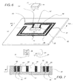
- Fig. 5 shows one embodiment of substrate 22 that has a channel pattern 40 with antenna channels 60, a transponder channel 62 and junction channels 64 joining the antenna channels 60 to transponder channel 62.
- an antenna 74 is formed on substrate 22 by filling antenna channels 60 and junction channels 62 with a conductive material 66.
- conductive material 66 is applied to substrate 22 using a coating process.
- Various coating methods can be used to apply conductive material 66 to substrate 22, some of these will be described in greater detail below, however, by way of example, these coating techniques include, but are not limited to, roll coating, slit die coating, gravure coating, curtain coating, and ink jet coating. Using any of these coating methods, a layer of conductive material 66 and any appropriate solvents, carriers or other materials can be coated into channel pattern 40 on substrate 22.
- Conductive material 66 typically can comprise any conductive material. Examples of such materials include metals such as copper, aluminum and other materials having electrically conductive properties. As will be discussed in greater detail below, other materials can also be used for conductive material 66.
- Conductive material 66 can be applied from either aqueous or organic solvent coating formulations using any of the known coating techniques such as roller coating, gravure coating, air knife coating, rod coating, extrusion coating, blade coating, curtain coating, slide coating, and the like. Specific examples of such coating techniques are described in greater detail below. Other known coating and drying methods are described in further detail in Research Disclosure No. 308119, Published December 1989, pages 1007 to 1008. After coating, conductive material 66 is generally dried by simple evaporation, which can be accelerated by known techniques such as convection heating.
- One method for coating conductive material 66 onto substrate 22 and into channel pattern 40 is to coat conductive material 66 into the conduits by roll coating conductive material 66 into substrate 22 followed by removal of conductive material 66 located at raised areas 52 of channel pattern 40 by a scraping blade or reverse roll contacting the peaks of the conduits.
- conductive material 66 is heated to a state that allows conductive material 66 to be coated onto channel pattern 40 of substrate 22.
- conductive material 66 can be combined with other materials to facilitate application of conductive material 66 to substrate 22 during the coating process. Examples of such other materials include plastics, solvents, carriers, binders and/or other materials.
- conductive material 66 flows into antenna channels 60, transponder channel 62 and junction channels 64 and at least partially fills these channels.
- Conductive material 66 is allowed to solidify for example as a result of the cooling of conductive material 66, the evaporation of solvents or carriers, or the application of a curative agent or energy source that activates a binder.
- the coating process is typically applied so that conductive material 66 flows or is mechanically scraped off of raised surfaces 52 and into channels 54. Once solidified, conductive material 66 provides an antenna 74 and other electrical circuit components such as electrical pathways and components.
- substrate 22 has a transponder channel 62 that is adapted to receive a transponder 70.
- transponder 70 is provided in transponder channel 62 prior to the application of the coating of conductive material 66.
- Transponder 70 has antenna engagement surfaces 72 adapted to engage antenna 74 or an electrical path leading to antenna 74.
- the conductive material 66 in junction channel 64 joins to the antenna engagement surfaces 72 of transponder 70 while conductive material 66 is still in a fluid or semi-fluid state.
- conductive material 66 solidifies to form an antenna 74
- conductive material 66 in junction channel 64 forms an electrical connection with antenna engagement surfaces 72.
- transponder 70 is positioned in transponder channel 62 after coating. This can occur, for example, before the coating of conductive material 66 has solidified.
- transponder 70 can be joined to the coating of conductive material 66 after conductive material 66 has solidified to form antenna 74.
- transponder 70 can be mechanically pressed into contact with the conductive material 66 in junction channels 64 to form an electrical connection.
- junction channels 64 can be omitted and antenna engagement surfaces 72 can be pressed directly into contact with antenna 74.
- a power supply circuit 76 in transponder 70 can receive electromagnetic signals and convert such signals into power to operate the transponder 70.
- a radio frequency communication circuit 78 transmits radio frequency signals that contain data that is stored in a memory 80.
- Radio frequency communication circuit 78 can also be adapted to use the electrical connection between antenna engagement surfaces 72 and antenna 74 to receive radio frequency signals having data and to store the data from such signals in memory 80.
- antenna 74 can be omitted where transponder 70 contains an integral antenna.
- transponder channel 62 has a width dimension 90 that is at least equal to a width dimension 82 of transponder 70.
- width dimension 90 of transponder channel 62 can be undersized with respect to width dimension 82 of transponder 70.
- insertion of transponder 70 into transponder channel 62 causes deformation of raised areas 52 of substrate 22 proximate to transponder channel 62 to allow transponders 70 to be inserted into transponder channel 62.
- thermoplastic material 26 in raised areas 52 of substrate 22 proximate to transponder channel 62 resists this deformation and applies a force against transponder 70.
- This force tends to hold transponder 70 within transponder channel 62 and can be used to hold transponder 70 so that antenna engagement surfaces 72 remain in contact with antenna 74 and hold transponder 70 in transponder channel 62, for example, during a coating operation where transponder 70 is positioned in the transponder channel 62 prior to coating.
- a medium 99 is formed when transponder 70 is joined to substrate 22 and forms an electrical connection with conductive material 66.
- Figs. 8 and 9 show medium 99 having a transponder 70 with a memory 80, an antenna 74 and an electrical connection between transponder 70 and antenna 74 defined by conductive material 66 in junction channel 64.
- raised areas 52 are separated from channels 54 by a distance 92 that is at least as great as a thickness 84 of transponder 70.
- antenna channels 60, and junction channel 64 can be filled with conductive material 66 to a level that fills antenna channels 60 and junction channels 64 are also filled to the level of raised areas 52.
- raised areas 52 and an outer surface 86 of transponder 70 and outer surfaces 88 of conductive material 66 form a common plane A - A to provide a level surface that can be processed without risk of interference with later material handling.
- This permits the use of useful medium fabrication processes such as rolling or extrusion after transponder 70 has been joined to substrate 22 and lowers the risk damage to previous and/or subsequently applied layers of where medium 99 is wound onto rolls for storage or during further processing.
- a substrate can be formed from transparent thermoplastic material 126 and conductive material 66 can be used that provides such transparency or substantially transparent, not withstanding the presence of conductive material 66 by providing very thin layers of such metals. Other materials can also be used for conductive material 66, some of which can be made transparent in relatively thicker applications.
- Transparent describes the ability of a medium to transmit "light” that is in the visible range and describes a condition where the total light transmission of the medium is 75% or greater at 500 nm.
- the term “diffuse light transmission” means the percentage of diffusely transmitted light at 500 nm as compared to the total amount of light at 500 nm of the light source.
- total light transmission means percentage of light transmitted through the sample at 500 nm. This includes both spectral and diffuse transmission of light.
- diffuse light transmission efficiency means the ratio of the percentage of diffuse transmitted light at 500 nm to the percentage of total transmitted light at 500 nm multiplied by a factor of 100.
- Having a transparent conductive material 66 is particularly useful because the layers behind it such as substrate 22, and/or base 28 can still be seen.
- conductive material 66 can be used for conductive material 66 that have a high visible light transmission characteristically useful in providing essentially transparent conductive pathways for use in forming antennas and other structures in a medium for example.
- conductive polymers can be used.
- Such “polymers” include homo- and co-polymers and such polymers can be selected from the group consisting of substituted or unsubstituted aniline containing polymers, substituted or unsubstituted pyrrole containing polymers, substituted or unsubstituted thiophene containing polymers.
- the above polymers provide the desired conductivity, adhesion to other layers in the validation device and have high light transmission.
- Conductive material 66 can also be coated from a coating composition comprising a polythiophene/polyanion composition containing an electrically conductive polythiophene with conjugated polymer backbone component and a polymeric polyanion component.
- a preferred polythiophene component for use in accordance with the present invention contains thiophene nuclei substituted with at least one alkoxy group, e.g., a C1 -C12 alkoxy group or a --O(CH2H2O)n CH3 group, with n being 1 to 4, or where the thiophene nucleus is ring closed over two oxygen atoms with an alkylene group including such group in substituted form.
- Electrically-conductive polythiophene/polyanion polymer compositions that can also be used to form conductive material 66 include 3,4-dialkoxy substituted polythiophene/poly(styrene sulfonate), with the most preferred electrically-conductive polythiophene/polyanion polymer composition being poly(3,4-ethylene dioxythiophene)/poly(styrene sulfonate), which is available commercially from Bayer Corporation as Baytron P.
- conductive material 66 can comprise pentacene.
- Pentacene is usefully employed because it is electrically conductive, can be made transparent, has high electron mobility and can easily be coated into channels 54 by known methods such as roll coating and doctor blade coating and other coating techniques, some of which are described in greater detail below.
- conductive material 66 can comprise materials that can be transferred such as those that that have been described for use in the photographic film arts to dissipate static charge.
- ionic conductors such as conjugated conducting polymers, conducting carbon particles, crystalline semiconductor particles, and amorphous semiconductive fibrils can be used.
- continuous semi-conducting thin films can be used more effectively than ionic conductors to conduct charge since their electrical conductivity is independent of relative humidity and only slightly influenced by ambient temperature.
- electrically conducting metal-containing particles such as semi-conducting metal oxides
- suitable polymeric film-forming binders in combination with polymeric non-film-forming particles as described in U.S. Pat. Nos. 5,340,676; 5,466,567; 5,700,623.
- Binary metal oxides doped with appropriate donor heteroatoms or containing oxygen deficiencies have been disclosed in prior art to be useful in antistatic layers for photographic films, for example, U.S. Pat. Nos.
- Suitable conductive metal oxides include: zinc oxide, titania, tin oxide, alumina, indium oxide, silica, magnesia, zirconia, barium oxide, molybdenum trioxide, tungsten trioxide, and vanadium pentoxide.
- Preferred doped conductive metal oxide granular particles include antimony-doped tin oxide, fluorine-doped tin oxide, aluminum-doped zinc oxide, and niobium-doped titania. Additionally conductive ternary metal oxides disclosed in U.S. Pat. No. 5,368,995 include zinc antimonate and indium antimonite can be used for conductive material 66. Other conductive metal-containing granular particles including metal borides, carbides, and nitrides have been disclosed in Japanese Kokai No. JP 04-055,492 and can be used for conductive material 66.
- conductive material 66 Yet another type of material that can be used for conductive material 66 is described in U.S. Pat. No. 6,096,491 which describes imaging elements, including motion imaging films, containing an electrically conductive layer protected under an abrasion resistant topcoat.
- the electrically-conductive layer may comprise an electrically conductive 3,4-dialkoxy substituted polythiophene styrene sulfonate complex.
- Any polymeric film-forming binder including water soluble polymers, synthetic latex polymers such as acrylics, styrenes, acrylonitriles, vinyl halides, butadienes, and others, or water dispersible condensation polymers such as polyurethanes, polyesters, polyester ionomers, polyamides, epoxides, and the like, may be optionally employed in the conductive material 66 to improve integrity of conductive material 66 and to improve adhesion of the conductive material 66 to an underlying and/or overlying layer.
- Preferred binders include polyester ionomers, vinylidene chloride containing interpolymers and sulfonated polyurethanes as disclosed in U.S. Pat. No.
- the electrically-conductive polythiophene/polyanion composition to added binder weight ratio can vary from 100:0 to 0.1:99.9, preferably from 1:1 to 1:20, and more preferably from 1:2 to 1:20.
- the dry coverage of the electrically-conductive substituted or unsubstituted thiophene-containing polymer employed depends on the inherent conductivity of the electrically-conductive polymer and the electrically-conductive polymer to binder weight ratio.
- a preferred range of dry coverage for the electrically-conductive substituted or unsubstituted thiophene-containing polymer component of the polythiophene/polyanion compositions is from about 0.5 mg/m.sup.2 to about 3.5 mg/m.sup.2. This dry coverage should provide the desired electrical resistivity values before and after photographic processing while minimizing the impact of the electrically-conductive polymer on the color and optical density of the processed photographic element.
- the conductive material 66 of the invention may include crosslinking agents, coating aids and surfactants, dispersing aids, coalescing aids, biocides, matte particles, waxes and other lubricants.
- a common level of coating aid in the conductive coating formula e.g., is 0.01 to 0.3 weight % active coating aid based on the total solution weight.
- These coating aids are typically either anionic or nonionic and can be chosen from many that are applied for aqueous coating.
- the various ingredients of the coating solution may benefit from pH adjustment prior to mixing, to insure compatibility. Commonly used agents for pH adjustment are ammonium hydroxide, sodium hydroxide, potassium hydroxide, tetraethyl amine, sulfuric acid, acetic acid, etc.
- Figs. 10 - 16 show various embodiments of coating methods that can be used to apply conductive material 66 to substrate 22.
- Figs. 10 and 11 show one example of a gap coating method.
- a supply 100 of conductive material 66 is applied to substrate 22 using a convenient means adapted for such material.
- Substrate 22 and the supply of conductive material 66 applied to web substrate 22 are passed between a roller 102 and limiting structure 104 such as a knife.
- limiting structure 104 removes excess conductive material 66 from raised areas 52.
- Conductive material 66 is then permitted to solidify. This provides a medium 99 having a transponder 70 with an antenna 74 and a uniform outer surface 106.
- Fig. 12 shows another embodiment of a method for coating conductive material 66 onto substrate 22.
- This coating method is known as curtain coating.
- conductive material 66 is processed to a liquid form and flows from a supply 110 in a continuous curtain 112 onto substrate 22 as substrate 22 is passed through curtain 112.
- curtain coating conductive material 66 flows off of raised area 52 into channel 54 such as antenna channel 60, transponder channel 62 and junction channel 64.
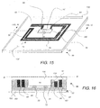
- Figs. 13 and 14 show still another embodiment of a method for coating a substrate 22.
- a technique known as slot die coating is used.
- a supply 120 has a slot 122 that ejects conductive material 66 onto patterned surface 42 of substrate 22 to fill or at least partially fill channel 54 such as antenna channel 60, transponder channel 62 and/or junction channel 64.
- an overcoat layer 130 can be applied to medium 99. Overcoat layer 130 secures transponder 70 and antenna 74 in medium 99. Further, overcoat layer 130 can be adapted to prevent conductive material 66 from being exposed after overcoat layer 130 has been applied. Overcoat layer 130 can also be adapted to receive image-forming materials. In the embodiment that is shown in Figs. 15 and 16, overcoat layer 130 is applied to form an outer surface 132 along plane B - B that does not have protrusions or other non-uniform areas. Overcoat layer 130 can also be adapted to cushion and protect transponder 70, antennas 74 and medium 99 from chemical, thermal, radiation or mechanical damage during handling or manipulation of medium 99. In the embodiment shown in Figs.
- overcoat layer 130 is shown as being transparent, however, in other embodiments, overcoat layer 130 can comprise a non-transparent material. To enhance adhesion of the overcoat layer 130 to conductive material 66, overcoat layer 130 can have a surface energy that is greater than 44 dynes per cm 2 .
- overcoat layer 130 separation 92 between raised areas 52 and channels 51 is at least as great as the thickness 79 of transponder 70 to achieve an outer surface having a common plane.
- a common plane e.g. B-B
- overcoat layer 130 can be used to form a common plane B-B on medium 99 even where, as is shown in Fig. 16, one or more of channels 54 is only partially filled with conductive material 66.
- overcoat layer 130 can comprise a transparent material that blocks the flow of ultraviolet or other forms of radiation, that provides protection against mechanical, thermal, chemical or other factors that may damage the appearance of the images formed on substrate 22.
- Figs. 15 and 16 show another optional feature in that the embodiment shown in these figures has an adhesive layer 150 that can be applied to base surface 46 or patterned surface 42 of medium 99 to permit medium 99 to be easily applied to a tangible thing such as a bottle.
- An advantage of such a medium is that a label can be provided that does not have a protrusion that might interfere with or be easily damaged by use and handling of the tangible thing to which medium 99 is attached.
- a removable layer 152 can be applied to adhesive layer 150.
- Adhesive layer 150 can comprise a pressure sensitive adhesive.
- a pressure sensitive adhesive is clear polymer such as acrylic or urethane.
- Temperature and chemical resistance in the adhesive is also preferred as medium 99 may be subjected to temperatures in excess of 80 degrees C and exposed to caustic chemistry.
- the pressure sensitive adhesive is preferably applied to base surface 46 opposite the pattern formed on substrate 22 to allow channel pattern 40 to be exposed.
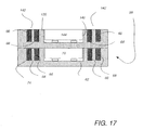
- overcoat layer 130 can also comprise a second patterned surface 140 in which a second antenna 142 and second transponder 146 can be formed using the techniques described above. It this way, media can be assembled having multiple layers of transponders or other electronic components. This allows for multi-dimensional components to be assembled in medium 99.
- Such components include, but not limited to, structures such as inductors and capacitors.
- substrate 22 can comprise both a patterned surface 42 and a second patterned surface 140 and have a base channel pattern 142 in which a second antenna 144 and second transponder 146 can be provided.
- substrate 22 can be formed using the embodiment of Figs. 1 or 2 with a pressure roller 34 that has a base roller pattern (not shown) that impresses a second patterned surface into base surface 46.
- second antenna 144 can be formed in the second patterned surface 140 using the same coating techniques described above.
- a second transponder 146 can also be applied in the manner described above.
- medium 99 is formed having a transponder 70 with an antenna 74 and a memory 80 formed therein.
- the dimensions of medium 99 have been defined to ensure that medium 99 is free of protrusions and provides uniform outer surfaces. This permits medium 99 to be further processed as necessary using conventional web forming techniques such as winding, rolling, extruding and printing.
- medium 99 having multiple transponders 70 attached thereto can be slit and wound onto rolls with each roll having at least one transponder 70.
- Medium 99 can also be slit and chopped into sheet form with each sheet having a transponder 70 associated therewith. It will be appreciated however, that this is an optional fraction.
- transponder 70 can be formed in whole or in part by defining channel pattern 40 on substrate 22 that is adapted to receive conductive material 66 and to arrange the received conductive material 66 to form useful components of transponder 70 including, but not limited to, components of the power supply circuit 76, radio frequency circuit 78 and memory 80.
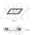
- substrate 22 can have a channel pattern 40 with channels 54 adapted to receive discrete components and other channels adapted to provide electrical pathways between the discrete components and other discrete components when conductive material 66 is deposited therein. For example, as is shown in Figs.
- a resistor 160 can be formed by providing a resistor channel 162 having a reduced cross sectional area relative to other channels or by only partially filling a channel with conductive material 66. As is shown in Figs. 19 and 20, the cross sectional area for resistor 160 is provided by reducing a width dimension 164 of resistor channel 162 and a depth dimension 166 which is the overall separation between the resistor channel 162 and adjacent raised portions 168.
- An electrically resistive material can be applied to antenna material 62 in the area of resistor 160.
- conductive material 66 can form other components such as a capacitor (not shown) by applying conductive material 66 along parallel channels separated by a relatively thin raised area 52.
- Other circuit components of transponder 70 can be formed in like fashion. From this, it will be appreciated that the shape of channel 54 can be adjusted to provide a gradient, step or other variation in three dimensional space within channel pattern 40. Depth dimension 166 of channels 54 can be varied to accommodate structures such as transponder 70, a capacitor (not shown) or other preformed components that can be assembled to substrate 22 to cooperate with transponder 70. Further, channel pattern 40 on substrate 22 can be defined so that entire circuits such as power supply circuit 76, radio frequency communication circuit 78 and/or memory 80, are formed by the application of conductive material 66 to channel pattern 40.
- the overall thickness of conductive material 66 and medium thickness 84 can be made thin.
- the thickness of channel 54 as defined by the separation between channel 54 and adjacent raised area 52, or the thickness of conductive material 66 applied in channel 54 can be made thin such as in the range of 1 to 20 microns which is a significant improvement over the minimum trace thickness of 25 microns typically used in forming conductive patterns using conductive inks.
- the density of channels can be significantly greater than is practical in systems that form conductive patterns using conductive inks. This is because the dimensional stability of roller pattern 40 and the dimensional accuracy of the placement of channel 54 permits highly accurate placement of the conductive channels without risk of bleeding created when conductive ink is used to form circuit patterns on a substrate.
- Another advantage of the use of channel 54 to determine electrical pathways in medium 99 is that channel 54 protects and separates the conductive material 66 from incidental abrasive damage that can significantly reduce the performance of antennas and other conductors.
- a further advantage of the use of channel 54 to define electrical pathways is that the raised areas 52 between channel 54 can serve to provide a dielectic material useful in forming advanced components such as capacitors on substrate 22.
- antenna pattern 60 and antenna 74 is shown.
- shape and arrangement of pattern 60 and antenna 74 are shown by way of example and not limitation. Any known antenna pattern that can be usefully employed to receive and send electromagnetic signals containing energy and information can be used.
- antenna patterns such the one disclosed in the '983 patent can be used.
- an antenna pattern is shown having an antenna coil with a first end connected to a transponder device. A second end of the coil feeds back to the transponder device. To do this the second end passes over the coils to the transponder.
- An insulator is positioned to separate second end from the coils as it passes over the coils.
- Such structures can be formed in accordance with the present invention, by forming medium 99 with multiple layers such as can be formed using substrate 22 having a channel pattern 40 on one side and a base channel pattern 140 formed on the other and forming the channel pattern 40 and base channel pattern 140 in a cooperative manner.
- One way of doing this is to define channel pattern 40 and base channel pattern 140 to form at least one passage through substrate 22 to allow electrical connections to be formed between structures formed in channel pattern 40 and base channel pattern 140.
- a channel pattern 40 can be formed on a substrate 22 with a transponder channel, and a first end and coil of an antenna pattern.
- a first passage can also be formed between antenna pattern portion of channel pattern 40 and a base channel pattern 140.
- Base channel pattern 140 can define a conductive path from the antenna coil to a second passageway that returns to the transponder so that the circuit between the transponder and antenna coil is completed.
- conductive paths can be formed in one or more overcoat with passages defined therethrough to engage conductive paths in an channel pattern 40 or base channel pattern 140 so that circuits formed in the overcoat can be integrated with circuits in the channel pattern 40 or base channel pattern 140 that is overcoated.
Abstract
Description
- The present invention relates in general to the field of mediums and more particularly to mediums having electronic memory associated therewith.
- Thin mediums of material such as paper, film and fabric have many useful applications. Often images and information are recorded on such mediums. Where information regarding characteristics of a medium is known before an image is recorded on the medium, the recording process can be adjusted to improve the quality of the recording. Once a recording has been made on a medium it can be useful to associate information in a memory that is associated with the medium. Such information can include information that describes the chain of custody of the medium, the use of the medium, and who has accessed the medium. Other useful information can also be associated with the medium such as information that depicts information recorded on the medium. See for example, commonly assigned U.S. Pat. Appl. No. 10/161,514, entitled Virtual Annotation of a Recording on an Archival Media, filed by Kerr et al. on June 3, 2002.
- It is known to use Radio Frequency Identification (RFID) tags to provide an electronic memory and communication capabilities that allow information to be associated with a medium electronically. Such RFID tags typically comprise three principal elements, an antenna and transponder that cooperate to send and receive electromagnetic fields containing information, and a memory that stores information received by the transponder and provides stored information for use by the transponder. One example of such an RFID tag is shown in U.S. Pat. No. 4,857,953 entitled Single Chip Transponder Device filed by Carroll et al. on Feb 8, 1998.
- The RFID tag is adapted to exchange information with a co-designed reading/writing device. Information that is stored in an RFID tag that is joined to an item can later be used to track, identify and process the item. The RFID tag can also store other information that is to be associated with the item. A commercially available "TAG-IT INLAY"™ RFID tag available from Texas Instruments, Incorporated, Dallas, Texas, USA, can be used to provide identifying information about an item to which the RFID tag is attached. This relatively thin, flexible type of RFID tag can be used in applications that previously required a label or bar code. The RFID tags of the prior art are typically used for identification purposes, such as for employee badges, inventory control, and credit card account identification. The advantage of such RFID tags is that they are small in size, easy to communicate with and, unlike a bar coded item, do not require the item to be optically aligned to the reader or scanner.
- RFID tags have been proposed for use in applications with passports and credit cards, such as is disclosed in U.S. Patent No. 5,528,222 entitled Radio Frequency Circuit and Memory in Thin Flexible Package filed by Moskowitz et al. on September 9, 1994. These devices are useful for tracking the location, characteristics and usage of documents, books and packages. For example, such tags can be used to track the location of documents and track the chain of custody of such documents within a document management system.
- RFID tags are typically formed into a package such as an inlay, or a plastic, glass or ceramic housing. The RFID package is then joined to an item such as a document or book after the item has been fully assembled. The RFID tag often has an adhesive surface that is used to form a bond between the RFID tag and the item to which it is being joined. It is also known to use other ways of mechanically joining an RFID tag to an item. For example, an RFID tag can be joined to an item using a staple or other mechanical fastener.
- There is room for improvement in this arrangement. For example, a poor bond or poor mechanical joint between the RFID tag and the item can result in separation of the RFID tag from the item. This can defeat the purpose of joining the RFID tag to the item. Further, joining an RFID tag to an item increases the cost of the combined RFID tag and item because the RFID tag must include the cost of both the base and the fastener and the cost of labor associated with joining the RFID tag to the item. These costs can become significant where RFID tags are to be joined to a multiplicity of individual items, such as for example, individual sheets of a medium such as film or paper.
- Additionally, such RFID tags typically take the form of a patterned antenna located on a base having a transponder unit applied to the top of the antenna. Accordingly, such RFID tags have a non-uniform cross-sectional area. The non-uniform cross-section of the tag can make the tag vulnerable to incidental damage to contact during manufacturing, printing, use, storage and distribution. Further, such RFID tags can interfere with the appearance and use of the item.
- One approach for solving these problems is to incorporate RFID tags inside an item such as an identification badge. In one example, a clamshell type of outer casing in which the RFID electronics and antenna are deposited is provided. An example of such an identification badge is the ProxCard II proximity access card sold by HID Corporation, Irvine, CA, USA. Thinner cards are made by sandwiching the RFID electronics and antenna between sheets of laminate material. An example of such a badge is the ISO ThinCard also sold by HID Corporation. While this method of forming a card produces a card that is thinner than the clamshell type card, the card has an uneven cross-section with increased thickness in the area of the RFID electronics.
- These techniques, however, are not feasibly applied to the task of forming a thin medium such as paper, film and fabric. Such thin mediums are typically fabricated in high volumes using coating, extrusion and rolling techniques to convert pulp, gelatin or other material into thin sheets of material that are then processed into useful forms. The addition of a clamshell type structure known in the art is not practical or economically feasible in this type of production. The alternative lamination approach of the prior art is also not preferred because the increased thickness and uneven cross section caused by the presence of RFID electronics and antenna sandwiched between laminations can interfere with subsequent fabrication processes causing damage to fabrication equipment, the RFID electronics, the antenna or to the medium itself. Further, this uneven cross section can interfere with imaging equipment when a laminated medium having the RFID electronics and antenna is passed through equipment such as a printer that uses a medium after formation. This interference can damage the RFID tag, the medium and the equipment that uses the medium. The uneven cross section also can create a less than desirable appearance for the medium and images that are subsequently recorded thereon. Also, the antenna required to allow communication with the RFID electronics can cause the medium to be considerably larger and higher in cost if the medium is required to be transparent such as would be required for mediums such as an x-ray, an overhead or a lenticular or other display.
- Alternatively, RFID circuits or circuit components can be formed by printing conductive materials such as inks onto a surface of a medium. For example Parmond® VLTRFID circuit sold by Paralec Inc., Princetone, New Jersey, USA are made in the way other circuits can be made using conductor inks such as those sold by Flint Ink in Ann Arbor, Michigan, USA. However, it can be difficult to use such printing techniques to form high density patterns of conductors on a medium particularly at high volume media production rates.
- Thus, a need exists for a medium that has the ability to store and electronically exchange data. A need also exists for a medium with this ability that is also compatible with conventional web fabrication processes, or post fabrication uses of the medium. Further, a need exists for a medium that can provide an antenna or RFID electronics using essentially transparent structures if required.
- In one aspect of the invention, a method is provided for forming a medium. In accordance with the method a substrate is formed having a patterned surface with a channel pattern and a transponder having a memory is provided in the channel pattern. A conductive material is deposited in the channel pattern with the conductive material operatively associated with the transponder.
- In another aspect of the invention, a method is provided for forming a medium. In accordance with the method, a substrate web is formed with a patterned surface having a channel pattern. A transponder having a memory is provided in the channel pattern. A conductive material is coated into the channel pattern with the conductive material electrically contacting the transponder, wherein the channel pattern includes an antenna pattern and wherein conductive material coated into the antenna pattern forms an antenna operatively associated with the transponder.
- In still another aspect of the invention, a medium is provided. The medium has a substrate having a patterned surface with a channel pattern and a transponder having a memory positioned in a portion of the channel pattern. A conductive material is in another portion of the channel pattern, wherein the transponder and conductive material are operatively associated.
- In a further aspect of the invention, a medium is provided. The medium has a substrate having a channel pattern the channel pattern having a transponder channel adapted to receive a transponder and an antenna portion. A transponder having a memory is positioned in the transponder channel. A conductive material is deposited in the channel pattern and operatively associated with the transponder.
- A more complete understanding of the invention and its advantages will become apparent from the detailed description taken in conjunction with the accompanying drawings, wherein examples of the invention are shown, and identical reference numbers have been used, where possible, to designate identical elements that are common to the figures referenced below:
- Fig. 1 shows a first embodiment of an extrusion roll molding apparatus;
- Fig. 2 shows another embodiment of an extrusion roll molding apparatus;
- Fig. 3 shows an example of a substrate;
- Fig. 4 shows a cross section view of the example substrate of Fig. 3;
- Fig. 5 shows one embodiment of a substrate having a channel pattern with antenna channels, a transponder channel and junction channels;
- Fig. 6 shows a perspective view of the substrate of Fig. 5 with antenna channels formed thereon;
- Fig. 7 shows a cross section view of the embodiment of Fig. 6;
- Fig. 8 shows a perspective view of a medium formed in accordance with the invention;
- Fig. 9 shows a cross section view of the embodiment shown in Fig. 8;
- Fig. 10 shows one example of a coating method;
- Fig. 11 shows a cross-section view of the example of the coating method of Fig. 10;
- Fig. 12 is another embodiment of a coating method;
- Fig. 13 is a perspective view of yet another example of a coating method;
- Fig. 14 shows a cross section view of the coating method shown in Fig. 13;
- Fig. 15 shows another embodiment of the medium in accordance with the present invention;
- Fig. 16 shows a cross section view of the medium shown in Fig. 15;
- Fig. 17 shows yet another embodiment of a medium in accordance with the present invention.
- Fig. 18 shows yet another embodiment of a medium in accordance with the present invention;
- Fig. 19 shows yet another embodiment of a medium in accordance with the present invention;
- Fig. 20 shows a cross section view of the embodiment of the medium shown in Fig. 19.
-
- The present invention will be directed in particular to elements forming part of, or in cooperation more directly with the methods and mediums of the present invention. It is to be understood that elements not specifically shown or described may take various forms well known to those skilled in the art.
- The medium of the present invention is formed using a substrate having a pattern of raised areas and channels. Figs. 1 and 2 show alternative embodiments for the formation of such a substrate.
- Fig. 1 shows a schematic illustration of an overall arrangement of one embodiment of an extrusion
roll molding apparatus 20 for fabricating asubstrate 22. In this embodiment, anextruder 24 provides athermoplastic material 26, such as a polymer, onto a base 28 that can be formed from the same material asthermoplastic material 26 or that can be formed from different materials such as papers, films, fabrics or other useful base materials.Base 28 is fed from abase supply roll 30.Thermoplastic material 26 andbase 28 pass into anip area 32 between apressure roller 34 and apattern roller 36. Asthermoplastic material 26 passes through niparea 32,pressure roller 34 andpattern roller 36 press thethermoplastic material 26 ontobase 28 and aroller pattern 38 of raised surfaces and channels (not shown) onpattern roller 36 is impressed intothermoplastic material 26. Whenroller pattern 38 is impressed intothermoplastic material 26 some of the meltedthermoplastic material 26 fills channels (not shown) inroller pattern 38 to form raised areas (not shown) on a patternedsurface 42 ofsubstrate 22 and the balance ofthermoplastic material 26 is squeezed ontobase 28 forming channels (not shown). Accordingly, this forms apattern channel 40 having channels separated by raised areas (not shown) on a patternedsurface 42 ofthermoplastic material 26, the arrangement of raised areas and channels inchannel pattern 40 is the negative of the arrangement of raised areas and channels found onroller pattern 38.Thermoplastic material 26 is then cooled below a melting temperature ofthermoplastic material 26 andsubstrate 22 is then wound onto a substrate take uproll 44 for further processing as will be described in greater detail below. - Fig. 2 shows another embodiment of an extrusion
roll molding apparatus 20 that can be used to formsubstrate 22. In the embodiment of Fig. 2, extrusionroll molding apparatus 20 comprises anextruder 24 that meltsthermoplastic material 26. Meltedthermoplastic material 26 supplied byextruder 24 is pressed into niparea 32 betweenpressure roller 34 andpattern roller 36. Meltedthermoplastic material 26 passes material betweenpressure roller 34 andpattern roller 36 and is cooled below the melting temperature ofthermoplastic material 26 to formsubstrate 22. As meltedthermoplastic material 26 is passed through niparea 32 to formsubstrate 22, aroller pattern 38 onpattern roller 36 is impressed into meltedthermoplastic material 26 to form achannel pattern 40 of channels (not shown) separated by raised areas (not shown) on patternedsurface 42 ofsubstrate 22 that is the negative ofpattern roller 36.Substrate 22 is then wound onto a substrate take uproll 44 for further processing as will be described in greater detail below. - In the embodiment shown,
pattern roller 36 comprises a metallic roller such as chrome, copper or stainless steel into whichroller pattern 38 is formed. However, in other embodiments,pattern roller 36 can comprise a variety of forms. For example,pattern roller 36 can comprise any type of dimensionally stable roller or drum that is adapted so that a metallic plate, sleeve or other structure (not shown) havingroller pattern 38 formed thereon that can be joined topattern roller 36 to provide a metallic contact surface having the desiredroller pattern 38. This allows thesame pattern roller 36 to be used in conjunction with many different roller patterns simply by changing the sleeve, metallic plate or other structure havingroller pattern 38. - Forming
roller pattern 38 on ametallic pattern roller 36 or metallic plate, metallic sleeve or other metallic structure that can be joined topattern roller 36, provides protection to the precision geometry ofroller pattern 38, provides excellent mechanical wear properties and is an excellent conductor of heat and pressure.Roller pattern 38 can be formed onpattern roller 36, a plate, sleeve or other structure by known machining techniques, including but not limited to, techniques such as machining the desired pattern directly into the roller surface utilizing wire EDM tools, etching the pattern directly into the roller, growing the pattern by use of photolithography, machining the pattern using high energy lasers, diamond milling, ion beam milling or creation of a random pattern by bead blasting the roller followed by chrome plating. - In alternative embodiments,
pattern roller 36 or a sleeve, plate or other structure bearingroller pattern 38 can be formed using other non-metallic materials. Forexample pattern roller 36 can be formed from materials such as ceramics or certain plastics.Roller pattern 38 can be formed in such materials using known techniques including, but not limited to, casting, oblation, ion beam milling, printing and lithographic techniques such as gray scale lithography. - Figs. 3 and 4 show, respectively, a perspective and cross-section view of an example of
substrate 22 formed in accordance with the embodiment of Fig. 1. As is shown in Fig. 3,channel pattern 40 formed on patternedsurface 42 ofsubstrate 22 byroller pattern 38 can comprise various shapes, sizes and arrangements intended to facilitate particular electrical, magnetic, mechanical, optical or chemical structures as will be described in greater detail below. Each shape is defined by a raisedarea 52 andchannel 54. Fig. 3 shows examples of only a few of the possible shapes that can be formed on a patternedsurface 42 ofsubstrate 22. Other shapes include ordered arrays of triangles, continuous fluidic channels, pyramids, squares, rounded features, cylinders, and complex shapes with multiple sides. In certain embodiments, the separation between raisedarea 52 andchannel 54 can range from 0.1 micrometers to about 100 micrometers, however, in other embodiments the sizes of the separation can range between 0.5 micrometers and 200 micrometers. It has experimentally been found that such extrusion roll molding processes provides precision negative replication ofroller pattern 38. For example, it has been shown that where extrusion roll molding is used to formchannel pattern 40 on patternedsurface 42 ofsubstrate 22, the features ofchannel pattern 40 typically replicate the dimensions of the features ofroller pattern 38 at greater than 95% of the dimensional range. Such precision formation is possible even when formingsubstrate 22 operating at machine speeds in the 20 to 200 meter/min range. Accordingly, it is possible to reliably and economically form precise arrangements of raisedareas 52 andchannels 54 insubstrate 22. This allowssubstrate 22 to be used to define a platform for fabricating and assembling a wide variety of useful structures. -
Thermoplastic material 26 can comprise a variety of suitable materials. For example, polymers are generally low in cost, and can be efficiently formed into subsequent shapes utilizing known processes such as melt extrusion, vacuum forming and injection molding. Example polymers that can be used forthermoplastic material 26 include polyolefins, cyclo-olefins, polyesters, polyamides, polycarbonates, cellulosic esters, polystyrene, polyvinyl resins, polysulfonamides, polyethers, polyimides, polyvinylidene fluoride, polyurethanes, polyphenylenesulfides, polytetrafluoroethylene, polyacetals, polysulfonates, polyester ionomers, and polyolefin ionomers. Copolymers and/or mixtures of these polymers to can be used to obtain athermoplastic material 26 having specific mechanical or optical properties. Polyamides that can be used inthermoplastic material 26 include, but are not limited to, nylon 6,nylon 66, and mixtures thereof. Copolymers of polyamides are also suitable continuous phase polymers that can be used inthermoplastic material 26. An example of a useful polycarbonate is bisphenol-A polycarbonate. Cellulosic esters are also suitable for use asthermoplastic material 26 and include cellulose nitrate, cellulose triacetate, cellulose diacetate, cellulose acetate propionate, cellulose acetate butyrate, and mixtures or copolymers thereof. Polyvinyl resins that can be used inthermoplastic material 26 include polyvinyl chloride, poly(vinyl acetal), and mixtures thereof. Copolymers of vinyl resins can also be utilized. - In addition,
thermoplastic material 26 can comprise various known polyesters for the polymer features of the invention including those produced from aromatic, aliphatic or cycloaliphatic dicarboxylic acids of 4-20 carbon atoms and aiphatic or alicyclic glycols having from 2-24 carbon atoms. Examples of suitable dicarboxylic acids include, but are not limited to, terephthalic, isophthalic, phthalic, naphthalene dicarboxylic acid, succinic, glutaric, adipic, azelaic, sebacic, fumaric, maleic, itaconic, 1,4-cyclohexanedicarboxylic, sodiosulfoisophthalic and mixtures thereof. Examples of suitable glycols include, but are not limited to, ethylene glycol, propylene glycol, butanediol, pentanediol, hexanediol, 1,4-cyclohexanedimethanol, diethylene glycol, other polyethylene glycols and mixtures thereof. - Addenda is optionally added to
thermoplastic material 26 to improve the optical, mechanical, chemical, magnetic or electrical characteristics ofchannel pattern 40 of raisedarea 52 andchannel 54 formed inthermoplastic material 26. An example of such useful addenda that can be added include, but are not limited to, an optical brightener. An optical brightener is substantially colorless, fluorescent, organic compound that absorbs ultraviolet light and emits it as visible blue light. Examples include, but are not limited to, derivatives of 4,4'-diaminostilbene-2,2'-disulfonic acid, coumarin derivatives such as 4-methyl-7-diethylaminocoumarin, 1-4-Bis (O-Cyanostyryl) Benzol and 2-Amino-4-Methyl Phenol. Other useful addenda that can be added tothermoplastic material 26 include antistatic compounds, pigments, dyes, carbon black, polymer stabilizers or ultraviolet absorbers. - As is described above,
substrate 22 has a patternedsurface 42 with achannel pattern 40 formed by contact withroller pattern 38. As is shown in Fig. 4,substrate 22 also has abase surface 46 on a side ofsubstrate 22 that is opposite from patternedsurface 42. In certain embodiments,base surface 46 can be formed to receive image forming materials such as inks, dyes, toners, and colorants. This permits images to be formed, for example, onbase surface 46 using ink jet printing, thermal printing, contact press printing and other techniques. There are various ways in which this can be done. - Where
substrate 22 is formed using the extrusion roll molding apparatus described in Fig. 1,base surface 46 is a surface that is a component ofbase 28. Accordingly,base 28 can be formed from a material that is adapted to receive image forming materials. Alternatively,base 28 can also be formed from a material that forms images when exposed to energy such as thermal, electrical, optical, electro-magnetic or other forms of energy. Similarly, wheresubstrate 22 is formed using the extrusion roll molding apparatus described in Fig. 2,base surface 46 is formed fromthermoplastic material 26. Accordingly, in such an embodiment, athermoplastic material 26 can be used that is capable of receiving image forming materials or that is capable of forming an image when exposed to energy. In still another alternative embodiment,base surface 46 can be adapted by chemical or other treatments or coatings to receive image forming materials or to form images when exposed to energy. - In the embodiment shown in Figs. 3 and 4,
substrate 22 has a thickness betweenbase surface 46 andchannels 54 of approximately 100 microns. This provides rigidity and structure tosubstrate 22 that enableschannel pattern 40 to maintain dimensional stability. However, in certain applications,channel pattern 40 can contain one ormore channels 54 that are separated frombase surface 46 to a different degree and can form a passage throughsubstrate 22 and define an opening atbase surface 46. -
Channel pattern 40 formed onsubstrate 22 can also optionally be coated with coatings that improve the optical, physical, electrical or chemical characteristics of raisedareas 52 andchannels 54. Examples of such coatings include urethane for scratch resistance, hard coats, antiglare coatings, antireflection coatings, antistatic materials and dyes for changing the color of the polymer features. Coating methods that can be used to apply such coatings include, but are not limited to, roll coating, slit die coating, gravure coating, curtain coating, and ink jet coating. Such coatings can be applied in a uniform, random or controlled pattern. - It will be appreciated that
channel pattern 40 can be used to form a precise arrangement of shapes onsubstrate 22 at convenient mass production speeds. There are various ways in which this structure can be used. The following will describe the use ofsubstrate 22 having achannel pattern 40 that enable the formation of precise structures onsubstrate 22 to form a medium having a memory and communication system incorporated in the medium. - Fig. 5 shows one embodiment of
substrate 22 that has achannel pattern 40 withantenna channels 60, atransponder channel 62 andjunction channels 64 joining theantenna channels 60 totransponder channel 62. As is shown in Figs. 6 and 7, anantenna 74 is formed onsubstrate 22 by fillingantenna channels 60 andjunction channels 62 with aconductive material 66. As will be described later,conductive material 66 is applied tosubstrate 22 using a coating process. Various coating methods can be used to applyconductive material 66 tosubstrate 22, some of these will be described in greater detail below, however, by way of example, these coating techniques include, but are not limited to, roll coating, slit die coating, gravure coating, curtain coating, and ink jet coating. Using any of these coating methods, a layer ofconductive material 66 and any appropriate solvents, carriers or other materials can be coated intochannel pattern 40 onsubstrate 22. -
Conductive material 66 typically can comprise any conductive material. Examples of such materials include metals such as copper, aluminum and other materials having electrically conductive properties. As will be discussed in greater detail below, other materials can also be used forconductive material 66. -
Conductive material 66 can be applied from either aqueous or organic solvent coating formulations using any of the known coating techniques such as roller coating, gravure coating, air knife coating, rod coating, extrusion coating, blade coating, curtain coating, slide coating, and the like. Specific examples of such coating techniques are described in greater detail below. Other known coating and drying methods are described in further detail in Research Disclosure No. 308119, Published December 1989, pages 1007 to 1008. After coating,conductive material 66 is generally dried by simple evaporation, which can be accelerated by known techniques such as convection heating. One method for coatingconductive material 66 ontosubstrate 22 and intochannel pattern 40 is to coatconductive material 66 into the conduits by roll coatingconductive material 66 intosubstrate 22 followed by removal ofconductive material 66 located at raisedareas 52 ofchannel pattern 40 by a scraping blade or reverse roll contacting the peaks of the conduits. Typically,conductive material 66 is heated to a state that allowsconductive material 66 to be coated ontochannel pattern 40 ofsubstrate 22. Alternatively,conductive material 66 can be combined with other materials to facilitate application ofconductive material 66 tosubstrate 22 during the coating process. Examples of such other materials include plastics, solvents, carriers, binders and/or other materials. - During coating,
conductive material 66 flows intoantenna channels 60,transponder channel 62 andjunction channels 64 and at least partially fills these channels.Conductive material 66 is allowed to solidify for example as a result of the cooling ofconductive material 66, the evaporation of solvents or carriers, or the application of a curative agent or energy source that activates a binder. The coating process is typically applied so thatconductive material 66 flows or is mechanically scraped off of raisedsurfaces 52 and intochannels 54. Once solidified,conductive material 66 provides anantenna 74 and other electrical circuit components such as electrical pathways and components. - In the embodiments of Figs. 5 - 9,
substrate 22 has atransponder channel 62 that is adapted to receive atransponder 70. In one embodiment of the present invention,transponder 70 is provided intransponder channel 62 prior to the application of the coating ofconductive material 66.Transponder 70 has antenna engagement surfaces 72 adapted to engageantenna 74 or an electrical path leading toantenna 74. Whenconductive material 66 is applied, theconductive material 66 injunction channel 64 joins to the antenna engagement surfaces 72 oftransponder 70 whileconductive material 66 is still in a fluid or semi-fluid state. Whenconductive material 66 solidifies to form anantenna 74,conductive material 66 injunction channel 64 forms an electrical connection with antenna engagement surfaces 72. In an alternative embodiment,transponder 70 is positioned intransponder channel 62 after coating. This can occur, for example, before the coating ofconductive material 66 has solidified. - Alternatively,
transponder 70 can be joined to the coating ofconductive material 66 afterconductive material 66 has solidified to formantenna 74. In this regard,transponder 70 can be mechanically pressed into contact with theconductive material 66 injunction channels 64 to form an electrical connection. In still another alternative,junction channels 64 can be omitted and antenna engagement surfaces 72 can be pressed directly into contact withantenna 74. - Using the electrical connection between
transponder 70 andantenna 74, apower supply circuit 76 intransponder 70 can receive electromagnetic signals and convert such signals into power to operate thetransponder 70. Whentransponder 70 is operated, a radiofrequency communication circuit 78 transmits radio frequency signals that contain data that is stored in amemory 80. Radiofrequency communication circuit 78 can also be adapted to use the electrical connection between antenna engagement surfaces 72 andantenna 74 to receive radio frequency signals having data and to store the data from such signals inmemory 80. In alternative embodiments,antenna 74 can be omitted wheretransponder 70 contains an integral antenna. - In the embodiment shown in Figs. 6 and 7
transponder channel 62 has awidth dimension 90 that is at least equal to awidth dimension 82 oftransponder 70. Alternatively, wheresubstrate 22 is formed from a material having a degree of elasticity,width dimension 90 oftransponder channel 62 can be undersized with respect towidth dimension 82 oftransponder 70. Wheretransponder channel 62 is undersized, insertion oftransponder 70 intotransponder channel 62 causes deformation of raisedareas 52 ofsubstrate 22 proximate totransponder channel 62 to allowtransponders 70 to be inserted intotransponder channel 62. However,thermoplastic material 26 in raisedareas 52 ofsubstrate 22 proximate totransponder channel 62 resists this deformation and applies a force againsttransponder 70. This force tends to holdtransponder 70 withintransponder channel 62 and can be used to holdtransponder 70 so that antenna engagement surfaces 72 remain in contact withantenna 74 and holdtransponder 70 intransponder channel 62, for example, during a coating operation wheretransponder 70 is positioned in thetransponder channel 62 prior to coating. A medium 99 is formed whentransponder 70 is joined tosubstrate 22 and forms an electrical connection withconductive material 66. - Figs. 8 and 9 show medium 99 having a
transponder 70 with amemory 80, anantenna 74 and an electrical connection betweentransponder 70 andantenna 74 defined byconductive material 66 injunction channel 64. As is shown in this embodiment, raisedareas 52 are separated fromchannels 54 by adistance 92 that is at least as great as athickness 84 oftransponder 70. Further, in this embodiment,antenna channels 60, andjunction channel 64 can be filled withconductive material 66 to a level that fillsantenna channels 60 andjunction channels 64 are also filled to the level of raisedareas 52. In this way, raisedareas 52 and anouter surface 86 oftransponder 70 andouter surfaces 88 ofconductive material 66 form a common plane A - A to provide a level surface that can be processed without risk of interference with later material handling. This permits the use of useful medium fabrication processes such as rolling or extrusion aftertransponder 70 has been joined tosubstrate 22 and lowers the risk damage to previous and/or subsequently applied layers of where medium 99 is wound onto rolls for storage or during further processing. - In certain embodiments it can be desirable for medium 99 to be transparent. In these embodiments a substrate can be formed from transparent thermoplastic material 126 and
conductive material 66 can be used that provides such transparency or substantially transparent, not withstanding the presence ofconductive material 66 by providing very thin layers of such metals. Other materials can also be used forconductive material 66, some of which can be made transparent in relatively thicker applications. As used herein, the term "Transparent" describes the ability of a medium to transmit "light" that is in the visible range and describes a condition where the total light transmission of the medium is 75% or greater at 500 nm. The term "diffuse light transmission" means the percentage of diffusely transmitted light at 500 nm as compared to the total amount of light at 500 nm of the light source. The term "total light transmission" means percentage of light transmitted through the sample at 500 nm. This includes both spectral and diffuse transmission of light. The term "diffuse light transmission efficiency" means the ratio of the percentage of diffuse transmitted light at 500 nm to the percentage of total transmitted light at 500 nm multiplied by a factor of 100. - Having a transparent
conductive material 66 is particularly useful because the layers behind it such assubstrate 22, and/orbase 28 can still be seen. - Various conductive materials can be used for
conductive material 66 that have a high visible light transmission characteristically useful in providing essentially transparent conductive pathways for use in forming antennas and other structures in a medium for example, conductive polymers can be used. Such "polymers" include homo- and co-polymers and such polymers can be selected from the group consisting of substituted or unsubstituted aniline containing polymers, substituted or unsubstituted pyrrole containing polymers, substituted or unsubstituted thiophene containing polymers. The above polymers provide the desired conductivity, adhesion to other layers in the validation device and have high light transmission.Conductive material 66 can also be coated from a coating composition comprising a polythiophene/polyanion composition containing an electrically conductive polythiophene with conjugated polymer backbone component and a polymeric polyanion component. A preferred polythiophene component for use in accordance with the present invention contains thiophene nuclei substituted with at least one alkoxy group, e.g., a C1 -C12 alkoxy group or a --O(CH2H2O)n CH3 group, with n being 1 to 4, or where the thiophene nucleus is ring closed over two oxygen atoms with an alkylene group including such group in substituted form. The preparation of electrically conductive polythiophene/polyanion compositions and of aqueous dispersions of polythiophenes synthesized in the presence of polyanions, as well as the production of antistatic coatings from such dispersions is described in EP 0 440 957 (and corresponding U.S. Pat. No. 5,300,575), as well as, for example, in U.S. Pat. Nos. 5,312,681; 5,354,613; 5,370,981; 5,372,924; 5,391,472; 5,403,467; 5,443,944; and 5,575,898, the disclosures of which are incorporated by reference herein. These polythiophene/polyanion compositions are commercially available. - Electrically-conductive polythiophene/polyanion polymer compositions that can also be used to form
conductive material 66 include 3,4-dialkoxy substituted polythiophene/poly(styrene sulfonate), with the most preferred electrically-conductive polythiophene/polyanion polymer composition being poly(3,4-ethylene dioxythiophene)/poly(styrene sulfonate), which is available commercially from Bayer Corporation as Baytron P. - In another embodiment,
conductive material 66 can comprise pentacene. Pentacene is usefully employed because it is electrically conductive, can be made transparent, has high electron mobility and can easily be coated intochannels 54 by known methods such as roll coating and doctor blade coating and other coating techniques, some of which are described in greater detail below. - In other embodiments,
conductive material 66 can comprise materials that can be transferred such as those that that have been described for use in the photographic film arts to dissipate static charge. In this regard, ionic conductors such as conjugated conducting polymers, conducting carbon particles, crystalline semiconductor particles, and amorphous semiconductive fibrils can be used. Alternatively, continuous semi-conducting thin films can be used more effectively than ionic conductors to conduct charge since their electrical conductivity is independent of relative humidity and only slightly influenced by ambient temperature. - In still other embodiments, electrically conducting metal-containing particles, such as semi-conducting metal oxides, are particularly effective when dispersed in suitable polymeric film-forming binders in combination with polymeric non-film-forming particles as described in U.S. Pat. Nos. 5,340,676; 5,466,567; 5,700,623. Binary metal oxides doped with appropriate donor heteroatoms or containing oxygen deficiencies have been disclosed in prior art to be useful in antistatic layers for photographic films, for example, U.S. Pat. Nos. 4,275,103; 4,416,963; 4,495,276; 4,394,441; 4,418,141; 4,431,764; 4,571,361; 4,999,276; 5,122,445; 5,294,525; 5,382,494; 5,459,021; 5,484,694 and others. Suitable conductive metal oxides include: zinc oxide, titania, tin oxide, alumina, indium oxide, silica, magnesia, zirconia, barium oxide, molybdenum trioxide, tungsten trioxide, and vanadium pentoxide. Preferred doped conductive metal oxide granular particles include antimony-doped tin oxide, fluorine-doped tin oxide, aluminum-doped zinc oxide, and niobium-doped titania. Additionally conductive ternary metal oxides disclosed in U.S. Pat. No. 5,368,995 include zinc antimonate and indium antimonite can be used for
conductive material 66. Other conductive metal-containing granular particles including metal borides, carbides, and nitrides have been disclosed in Japanese Kokai No. JP 04-055,492 and can be used forconductive material 66. - Yet another type of material that can be used for
conductive material 66 is described in U.S. Pat. No. 6,096,491 which describes imaging elements, including motion imaging films, containing an electrically conductive layer protected under an abrasion resistant topcoat. The electrically-conductive layer may comprise an electrically conductive 3,4-dialkoxy substituted polythiophene styrene sulfonate complex. - Any polymeric film-forming binder, including water soluble polymers, synthetic latex polymers such as acrylics, styrenes, acrylonitriles, vinyl halides, butadienes, and others, or water dispersible condensation polymers such as polyurethanes, polyesters, polyester ionomers, polyamides, epoxides, and the like, may be optionally employed in the
conductive material 66 to improve integrity ofconductive material 66 and to improve adhesion of theconductive material 66 to an underlying and/or overlying layer. Preferred binders include polyester ionomers, vinylidene chloride containing interpolymers and sulfonated polyurethanes as disclosed in U.S. Pat. No. 6,124,083. The electrically-conductive polythiophene/polyanion composition to added binder weight ratio can vary from 100:0 to 0.1:99.9, preferably from 1:1 to 1:20, and more preferably from 1:2 to 1:20. The dry coverage of the electrically-conductive substituted or unsubstituted thiophene-containing polymer employed depends on the inherent conductivity of the electrically-conductive polymer and the electrically-conductive polymer to binder weight ratio. A preferred range of dry coverage for the electrically-conductive substituted or unsubstituted thiophene-containing polymer component of the polythiophene/polyanion compositions is from about 0.5 mg/m.sup.2 to about 3.5 mg/m.sup.2. This dry coverage should provide the desired electrical resistivity values before and after photographic processing while minimizing the impact of the electrically-conductive polymer on the color and optical density of the processed photographic element. - In addition to the electrically-conductive agent(s) and polymeric binder, the
conductive material 66 of the invention may include crosslinking agents, coating aids and surfactants, dispersing aids, coalescing aids, biocides, matte particles, waxes and other lubricants. A common level of coating aid in the conductive coating formula, e.g., is 0.01 to 0.3 weight % active coating aid based on the total solution weight. These coating aids are typically either anionic or nonionic and can be chosen from many that are applied for aqueous coating. The various ingredients of the coating solution may benefit from pH adjustment prior to mixing, to insure compatibility. Commonly used agents for pH adjustment are ammonium hydroxide, sodium hydroxide, potassium hydroxide, tetraethyl amine, sulfuric acid, acetic acid, etc. - Figs. 10 - 16 show various embodiments of coating methods that can be used to apply
conductive material 66 tosubstrate 22. Figs. 10 and 11 show one example of a gap coating method. In this method, asupply 100 ofconductive material 66 is applied tosubstrate 22 using a convenient means adapted for such material.Substrate 22 and the supply ofconductive material 66 applied toweb substrate 22 are passed between aroller 102 and limitingstructure 104 such as a knife. Asconductive material 66 andsubstrate 22 pass betweenroller 102 and limitingstructure 104, limitingstructure 104 removes excessconductive material 66 from raisedareas 52.Conductive material 66 is then permitted to solidify. This provides a medium 99 having atransponder 70 with anantenna 74 and a uniformouter surface 106. - Fig. 12 shows another embodiment of a method for coating
conductive material 66 ontosubstrate 22. This coating method is known as curtain coating. In curtain coating,conductive material 66 is processed to a liquid form and flows from asupply 110 in acontinuous curtain 112 ontosubstrate 22 assubstrate 22 is passed throughcurtain 112. When this occurs,conductive material 66 flows off of raisedarea 52 intochannel 54 such asantenna channel 60,transponder channel 62 andjunction channel 64. - Figs. 13 and 14 show still another embodiment of a method for coating a
substrate 22. In this embodiment, a technique known as slot die coating is used. In this technique, asupply 120 has aslot 122 that ejectsconductive material 66 onto patternedsurface 42 ofsubstrate 22 to fill or at least partially fillchannel 54 such asantenna channel 60,transponder channel 62 and/orjunction channel 64. - It will be appreciated that other techniques can also be used to apply conductive material to fill or at least partially fill
channel 54 ofchannel pattern 40 formed onsubstrate 22 including but not limited to spraying and printingconductive material 66 ontosubstrate 22. - As is shown in Figs. 15 and 16, in another embodiment, an
overcoat layer 130 can be applied tomedium 99.Overcoat layer 130 securestransponder 70 andantenna 74 inmedium 99. Further,overcoat layer 130 can be adapted to preventconductive material 66 from being exposed afterovercoat layer 130 has been applied.Overcoat layer 130 can also be adapted to receive image-forming materials. In the embodiment that is shown in Figs. 15 and 16,overcoat layer 130 is applied to form anouter surface 132 along plane B - B that does not have protrusions or other non-uniform areas.Overcoat layer 130 can also be adapted to cushion and protecttransponder 70,antennas 74 and medium 99 from chemical, thermal, radiation or mechanical damage during handling or manipulation ofmedium 99. In the embodiment shown in Figs. 15 and 16,overcoat layer 130 is shown as being transparent, however, in other embodiments,overcoat layer 130 can comprise a non-transparent material. To enhance adhesion of theovercoat layer 130 toconductive material 66,overcoat layer 130 can have a surface energy that is greater than 44 dynes per cm2. - Where an
overcoat layer 130 is used,separation 92 between raisedareas 52 and channels 51 is at least as great as the thickness 79 oftransponder 70 to achieve an outer surface having a common plane. This is because a common plane e.g. B-B, can be formed by anouter surface 132 ofovercoat layer 130 whereinovercoat layer 130 applied to a thickness that, in combination with adistance 92 of asubstrate 22 is at least co-extensive with the thickness oftransponder 70. Further,overcoat layer 130 can be used to form a common plane B-B on medium 99 even where, as is shown in Fig. 16, one or more ofchannels 54 is only partially filled withconductive material 66. - Where
substrate 22 has raisedareas 52 that are adapted to receive image forming materials, such image forming materials can be applied to form images on patternedsurface 42 beforeovercoat layer 130 is formed. In one such embodiment,overcoat layer 130 can comprise a transparent material that blocks the flow of ultraviolet or other forms of radiation, that provides protection against mechanical, thermal, chemical or other factors that may damage the appearance of the images formed onsubstrate 22. - Figs. 15 and 16 show another optional feature in that the embodiment shown in these figures has an
adhesive layer 150 that can be applied tobase surface 46 or patternedsurface 42 ofmedium 99 to permit medium 99 to be easily applied to a tangible thing such as a bottle. An advantage of such a medium is that a label can be provided that does not have a protrusion that might interfere with or be easily damaged by use and handling of the tangible thing to whichmedium 99 is attached. To facilitate handling of this adhesive embodiment ofmedium 99, aremovable layer 152 can be applied toadhesive layer 150.Adhesive layer 150 can comprise a pressure sensitive adhesive. One example of such a pressure sensitive adhesive is clear polymer such as acrylic or urethane. Temperature and chemical resistance in the adhesive is also preferred asmedium 99 may be subjected to temperatures in excess of 80 degrees C and exposed to caustic chemistry. The pressure sensitive adhesive is preferably applied tobase surface 46 opposite the pattern formed onsubstrate 22 to allowchannel pattern 40 to be exposed. - As is shown in Fig. 17,
overcoat layer 130 can also comprise a secondpatterned surface 140 in which asecond antenna 142 andsecond transponder 146 can be formed using the techniques described above. It this way, media can be assembled having multiple layers of transponders or other electronic components. This allows for multi-dimensional components to be assembled inmedium 99. Such components include, but not limited to, structures such as inductors and capacitors. - As is shown in Fig. 18,
substrate 22 can comprise both apatterned surface 42 and a secondpatterned surface 140 and have abase channel pattern 142 in which asecond antenna 144 andsecond transponder 146 can be provided. Conveniently,substrate 22 can be formed using the embodiment of Figs. 1 or 2 with apressure roller 34 that has a base roller pattern (not shown) that impresses a second patterned surface intobase surface 46. Similarly,second antenna 144 can be formed in the secondpatterned surface 140 using the same coating techniques described above. Further, asecond transponder 146 can also be applied in the manner described above. - Using the above described methods,
medium 99 is formed having atransponder 70 with anantenna 74 and amemory 80 formed therein. In certain embodiments, the dimensions ofmedium 99 have been defined to ensure thatmedium 99 is free of protrusions and provides uniform outer surfaces. This permits medium 99 to be further processed as necessary using conventional web forming techniques such as winding, rolling, extruding and printing. For example, medium 99 havingmultiple transponders 70 attached thereto can be slit and wound onto rolls with each roll having at least onetransponder 70.Medium 99 can also be slit and chopped into sheet form with each sheet having atransponder 70 associated therewith. It will be appreciated however, that this is an optional fraction. - In any embodiment described above,
transponder 70 can be formed in whole or in part by definingchannel pattern 40 onsubstrate 22 that is adapted to receiveconductive material 66 and to arrange the receivedconductive material 66 to form useful components oftransponder 70 including, but not limited to, components of thepower supply circuit 76,radio frequency circuit 78 andmemory 80. In thisregard substrate 22 can have achannel pattern 40 withchannels 54 adapted to receive discrete components and other channels adapted to provide electrical pathways between the discrete components and other discrete components whenconductive material 66 is deposited therein. For example, as is shown in Figs. 15 and 16, aresistor 160 can be formed by providing aresistor channel 162 having a reduced cross sectional area relative to other channels or by only partially filling a channel withconductive material 66. As is shown in Figs. 19 and 20, the cross sectional area forresistor 160 is provided by reducing awidth dimension 164 ofresistor channel 162 and adepth dimension 166 which is the overall separation between theresistor channel 162 and adjacent raisedportions 168. An electrically resistive material can be applied toantenna material 62 in the area ofresistor 160. - Further
conductive material 66 can form other components such as a capacitor (not shown) by applyingconductive material 66 along parallel channels separated by a relatively thin raisedarea 52. Other circuit components oftransponder 70 can be formed in like fashion. From this, it will be appreciated that the shape ofchannel 54 can be adjusted to provide a gradient, step or other variation in three dimensional space withinchannel pattern 40.Depth dimension 166 ofchannels 54 can be varied to accommodate structures such astransponder 70, a capacitor (not shown) or other preformed components that can be assembled tosubstrate 22 to cooperate withtransponder 70. Further,channel pattern 40 onsubstrate 22 can be defined so that entire circuits such aspower supply circuit 76, radiofrequency communication circuit 78 and/ormemory 80, are formed by the application ofconductive material 66 tochannel pattern 40. - It will be appreciated that in the embodiments shown and described above, the overall thickness of
conductive material 66 andmedium thickness 84 can be made thin. For example, the thickness ofchannel 54 as defined by the separation betweenchannel 54 and adjacent raisedarea 52, or the thickness ofconductive material 66 applied inchannel 54 can be made thin such as in the range of 1 to 20 microns which is a significant improvement over the minimum trace thickness of 25 microns typically used in forming conductive patterns using conductive inks. - It will also be appreciated that in accordance with the present invention, the density of channels can be significantly greater than is practical in systems that form conductive patterns using conductive inks. This is because the dimensional stability of
roller pattern 40 and the dimensional accuracy of the placement ofchannel 54 permits highly accurate placement of the conductive channels without risk of bleeding created when conductive ink is used to form circuit patterns on a substrate. Another advantage of the use ofchannel 54 to determine electrical pathways inmedium 99 is thatchannel 54 protects and separates theconductive material 66 from incidental abrasive damage that can significantly reduce the performance of antennas and other conductors. A further advantage of the use ofchannel 54 to define electrical pathways is that the raisedareas 52 betweenchannel 54 can serve to provide a dielectic material useful in forming advanced components such as capacitors onsubstrate 22. - In the embodiments shown above, one possible form of an
antenna pattern 60 andantenna 74 is shown. However, shape and arrangement ofpattern 60 andantenna 74 are shown by way of example and not limitation. Any known antenna pattern that can be usefully employed to receive and send electromagnetic signals containing energy and information can be used. For example, antenna patterns such the one disclosed in the '983 patent can be used. In the '983 patent, an antenna pattern is shown having an antenna coil with a first end connected to a transponder device. A second end of the coil feeds back to the transponder device. To do this the second end passes over the coils to the transponder. An insulator is positioned to separate second end from the coils as it passes over the coils. Such structures can be formed in accordance with the present invention, by formingmedium 99 with multiple layers such as can be formed usingsubstrate 22 having achannel pattern 40 on one side and abase channel pattern 140 formed on the other and forming thechannel pattern 40 andbase channel pattern 140 in a cooperative manner. One way of doing this is to definechannel pattern 40 andbase channel pattern 140 to form at least one passage throughsubstrate 22 to allow electrical connections to be formed between structures formed inchannel pattern 40 andbase channel pattern 140. - For example, to form an antenna of the type shown in the '983 patent, a
channel pattern 40 can be formed on asubstrate 22 with a transponder channel, and a first end and coil of an antenna pattern. A first passage can also be formed between antenna pattern portion ofchannel pattern 40 and abase channel pattern 140.Base channel pattern 140 can define a conductive path from the antenna coil to a second passageway that returns to the transponder so that the circuit between the transponder and antenna coil is completed. Similarly, conductive paths can be formed in one or more overcoat with passages defined therethrough to engage conductive paths in anchannel pattern 40 orbase channel pattern 140 so that circuits formed in the overcoat can be integrated with circuits in thechannel pattern 40 orbase channel pattern 140 that is overcoated. - The invention has been described in detail with particular reference to certain preferred embodiments thereof, but it will be understood that variations and modifications can be effected within the spirit and scope of the invention.
Claims (10)
- A method for forming a medium comprising the steps of:forming a substrate having a patterned surface with a channel pattern thereon;providing a transponder having a memory in the channel pattern; anddepositing a conductive material in the channel pattern with the conductive material operatively associated with the transponder.
- The method of claim 1 wherein the transponder has a thickness within a predefined range and wherein the step of forming the channel pattern comprises forming at least one channel having a depth that is greater than the thickness of the transponder and adapted to receive the transponder.
- The method of claim 1 wherein a portion of the channel pattern has a width dimension that is smaller in size than a width dimension of the transponder and the step of providing the transponder in the channel pattern recess comprises elastically deforming the substrate in the smaller portion to receive the transponder.
- The method of claim 1 further comprising the step of providing an overcoat layer on at least one side of the substrate said overcoat layer adapted to permit the formation of an image thereon.
- The method of claim 1, wherein the step of forming a substrate comprises passing a moldable thermoplastic material between a pressure roller and a patterned roller so that the moldable thermoplastic material is formed into a substrate having a channel pattern conforming to the roller pattern.
- The method of claim 1, wherein the step of forming a substrate comprises passing a base material and a moldable thermoplastic material between a pressure roller and a pattern roller having a roller pattern, so that the moldable thermoplastic material is joined to the base and has a channel pattern conforming to the roller pattern.
- A method for forming a medium comprising the steps of:forming a substrate web with a patterned surface having a channel pattern ;providing a transponder having a memory in the channel pattern; andcoating a conductive material into the channel pattern with the conductive material electrically contacting the transponder, wherein said channel pattern includes an antenna pattern and wherein conductive material coated into the antenna pattern forms an antenna operatively associated with the transponder.
- A medium comprising:a substrate having a patterned surface with a channel pattern;a transponder having a memory positioned in a portion of the channel pattern; anda conductive material in another portion of the channel pattern;wherein the transponder and conductive material are operatively associated.
- The medium of claim 48, wherein electrical components are positioned in the channel pattern and wherein conductive material deposited in the channel pattern forms electrical connections between the electrical components to form the transponder.
- A medium comprising:a substrate having a channel pattern the channel pattern having a transponder channel adapted to receive a transponder and an antenna portion;a transponder having a memory positioned in the transponder channel; anda conductive material deposited in the channel pattern and operatively associated with the transponder.
Applications Claiming Priority (2)
| Application Number | Priority Date | Filing Date | Title |
|---|---|---|---|
| US10/411,624 US7051429B2 (en) | 2003-04-11 | 2003-04-11 | Method for forming a medium having data storage and communication capabilities |
| US411624 | 2003-04-11 |
Publications (2)
| Publication Number | Publication Date |
|---|---|
| EP1467315A2 true EP1467315A2 (en) | 2004-10-13 |
| EP1467315A3 EP1467315A3 (en) | 2006-02-15 |
Family
ID=32869225
Family Applications (1)
| Application Number | Title | Priority Date | Filing Date |
|---|---|---|---|
| EP04076019A Withdrawn EP1467315A3 (en) | 2003-04-11 | 2004-03-29 | Medium having data storage and communication capabilities and method for forming same |
Country Status (3)
| Country | Link |
|---|---|
| US (1) | US7051429B2 (en) |
| EP (1) | EP1467315A3 (en) |
| JP (1) | JP2004318846A (en) |
Cited By (7)
| Publication number | Priority date | Publication date | Assignee | Title |
|---|---|---|---|---|
| WO2005054030A1 (en) * | 2003-12-05 | 2005-06-16 | Ansaldo Segnalamento Ferroviario S.P.A. | Railway beacon and related production method |
| FR2887160A1 (en) * | 2005-06-16 | 2006-12-22 | Eastman Kodak Co | Discontinuous layer forming process for e.g. display screen, involves penetrating prominent part of embossing device into continuous layer to push same quantity of thin layer material into each part of formed discontinuous layer |
| EP1788514A1 (en) * | 2005-11-21 | 2007-05-23 | Stmicroelectronics Sa | Electronic micromodule and method of fabrication |
| WO2010123925A3 (en) * | 2009-04-20 | 2011-01-20 | Flextronics Ap, Llc | Miniature rfid tag |
| FR2995709A1 (en) * | 2012-09-18 | 2014-03-21 | Arjowiggins Security | METHOD FOR MANUFACTURING ELECTRONIC CHIP STRUCTURE AND STRUCTURE THUS MANUFACTURED |
| CN106910633A (en) * | 2015-12-04 | 2017-06-30 | Nec东金株式会社 | Solid electrolyte capacitators |
| CN110892796A (en) * | 2017-08-01 | 2020-03-17 | 惠普发展公司,有限责任合伙企业 | Chipless RFID printing method |
Families Citing this family (33)
| Publication number | Priority date | Publication date | Assignee | Title |
|---|---|---|---|---|
| US7795076B2 (en) | 2003-06-12 | 2010-09-14 | Symbol Technologies, Inc. | Method, system, and apparatus for transfer of dies using a die plate having die cavities |
| US7370808B2 (en) * | 2004-01-12 | 2008-05-13 | Symbol Technologies, Inc. | Method and system for manufacturing radio frequency identification tag antennas |
| GB0405883D0 (en) * | 2004-03-16 | 2004-04-21 | Dupont Teijin Films Us Ltd | Polymeric film substrate |
| JP3947776B2 (en) * | 2004-05-13 | 2007-07-25 | ニスカ株式会社 | Conductive material and manufacturing method thereof |
| US7268063B1 (en) * | 2004-06-01 | 2007-09-11 | University Of Central Florida | Process for fabricating semiconductor component |
| US7679591B2 (en) * | 2004-07-09 | 2010-03-16 | Au Optronics Corporation | Light emitting display device |
| JP4328682B2 (en) * | 2004-07-13 | 2009-09-09 | 富士通株式会社 | Radio tag antenna structure for optical recording medium and optical recording medium housing case with radio tag antenna |
| WO2006076607A1 (en) * | 2005-01-14 | 2006-07-20 | Cabot Corporation | Ink-jet printing of passive electricalcomponents |
| JP4536552B2 (en) * | 2005-02-28 | 2010-09-01 | ケイ・アール・ディコーポレーション株式会社 | IC tag |
| US7714726B2 (en) | 2005-05-06 | 2010-05-11 | Dominic M. Kotab | Semi-transparent RFID tags |
| US7722920B2 (en) * | 2005-05-13 | 2010-05-25 | University Of Pittsburgh-Of The Commonwealth System Of Higher Education | Method of making an electronic device using an electrically conductive polymer, and associated products |
| US20070012773A1 (en) * | 2005-06-07 | 2007-01-18 | University Of Pittsburgh - Of The Commonwealth System Of Higher Education | Method of making an electronic device using an electrically conductive polymer, and associated products |
| JP2007072853A (en) * | 2005-09-08 | 2007-03-22 | Renesas Technology Corp | Method for manufacturing electronic apparatus |
| EP1821241A3 (en) * | 2006-02-15 | 2008-07-23 | Assa Abloy AB | Hybrid frequency contactless transponder unit, module for and method of manufacturing |
| US20080073007A1 (en) * | 2006-09-25 | 2008-03-27 | Maribeth Zuesi-Kreuzer | Verifiable Handbag |
| US20080103944A1 (en) * | 2006-10-30 | 2008-05-01 | Mobile Logistics Management L.L.C. | Intelligent Pallet |
| US20090033495A1 (en) * | 2007-08-03 | 2009-02-05 | Akash Abraham | Moldable radio frequency identification device |
| MX2010008213A (en) * | 2008-02-22 | 2010-09-30 | Toppan Printing Co Ltd | Transponder and book form. |
| KR20090099235A (en) * | 2008-03-17 | 2009-09-22 | 삼성전자주식회사 | Antenna structure |
| RU2532732C2 (en) * | 2008-08-29 | 2014-11-10 | Логомотион, С.Р.О. | Plug-in card for wireless communication, method for manufacture and use thereof |
| US9098845B2 (en) | 2008-09-19 | 2015-08-04 | Logomotion, S.R.O. | Process of selling in electronic shop accessible from the mobile communication device |
| WO2010128442A2 (en) | 2009-05-03 | 2010-11-11 | Logomotion, S.R.O. | A payment terminal using a mobile communication device, such as a mobile phone; a method of direct debit payment transaction |
| SK288641B6 (en) | 2008-10-15 | 2019-02-04 | Smk Corporation | Communication method with POS terminal and frequency convertor for POS terminal |
| US20100155128A1 (en) * | 2008-12-22 | 2010-06-24 | Tombs Thomas N | Printed electronic circuit boards and other articles having patterned coonductive images |
| US20100159648A1 (en) * | 2008-12-22 | 2010-06-24 | Tombs Thomas N | Electrophotograph printed electronic circuit boards |
| US8512933B2 (en) * | 2008-12-22 | 2013-08-20 | Eastman Kodak Company | Method of producing electronic circuit boards using electrophotography |
| US9508213B2 (en) * | 2010-03-22 | 2016-11-29 | Dominic M. Kotab | Systems and methods of reading gaming chips and other stacked items |
| US8649820B2 (en) | 2011-11-07 | 2014-02-11 | Blackberry Limited | Universal integrated circuit card apparatus and related methods |
| US9246214B2 (en) * | 2012-03-08 | 2016-01-26 | Apple Inc. | Electronic device antenna structures with ferrite layers |
| USD703208S1 (en) | 2012-04-13 | 2014-04-22 | Blackberry Limited | UICC apparatus |
| US8936199B2 (en) | 2012-04-13 | 2015-01-20 | Blackberry Limited | UICC apparatus and related methods |
| USD701864S1 (en) | 2012-04-23 | 2014-04-01 | Blackberry Limited | UICC apparatus |
| CN111542835A (en) * | 2017-12-01 | 2020-08-14 | 艾利丹尼森零售信息服务公司 | Flexible fabric label utilizing holes in a substrate |
Citations (6)
| Publication number | Priority date | Publication date | Assignee | Title |
|---|---|---|---|---|
| EP0841634A2 (en) * | 1996-11-08 | 1998-05-13 | ODS R. Oldenbourg Datensysteme GmbH & Co. KG | Method for manufacturing a chip card and device for implementing the method |
| US5962840A (en) * | 1994-12-23 | 1999-10-05 | Giesecke & Devrient Gmbh | Data carrier with electronic module and embedded coil feature |
| WO2001026180A1 (en) * | 1999-10-04 | 2001-04-12 | Amerasia International Technology, Inc. | Tamper-resistant wireless article including an antenna |
| WO2001037622A2 (en) * | 1999-11-18 | 2001-05-25 | Orga Kartensysteme Gmbh | Printed conductor support layer for laminating into a chip card, method for producing a printed conductor support layer and injection molding tool for carrying out the method for producing a printed conductor support layer |
| US6248199B1 (en) * | 1999-04-26 | 2001-06-19 | Soundcraft, Inc. | Method for the continuous fabrication of access control and identification cards with embedded electronics or other elements |
| US6329213B1 (en) * | 1997-05-01 | 2001-12-11 | Micron Technology, Inc. | Methods for forming integrated circuits within substrates |
Family Cites Families (37)
| Publication number | Priority date | Publication date | Assignee | Title |
|---|---|---|---|---|
| AU511943B2 (en) * | 1978-07-12 | 1980-09-11 | Matsushita Electric Industrial Co., Ltd. | Electrographic recording |
| JPS56143443A (en) * | 1980-04-11 | 1981-11-09 | Fuji Photo Film Co Ltd | Electrically conductive support for electrophotographic material |
| JPS56143430A (en) * | 1980-04-11 | 1981-11-09 | Fuji Photo Film Co Ltd | Photographic sensitive material with improved antistatic property |
| JPS5785866A (en) * | 1980-11-18 | 1982-05-28 | Mitsubishi Metal Corp | Antistatic transparent paint |
| JPS6049894B2 (en) * | 1980-12-23 | 1985-11-05 | 富士写真フイルム株式会社 | photographic material |
| JPS57118242A (en) * | 1981-01-14 | 1982-07-23 | Fuji Photo Film Co Ltd | Photographic sensitive material |
| JPS57165252A (en) * | 1981-04-06 | 1982-10-12 | Fuji Photo Film Co Ltd | Antistatic plastic film |
| US4604678A (en) * | 1983-07-18 | 1986-08-05 | Frederick Parker | Circuit board with high density electrical tracers |
| US4999276A (en) * | 1988-06-29 | 1991-03-12 | Fuji Photo Film Co., Ltd. | Silver halide photographic materials |
| JPH02164872A (en) | 1988-12-20 | 1990-06-25 | Mitsui Toatsu Chem Inc | Fluorine-containing guanamine compound and production thereof |
| DE3913857A1 (en) * | 1989-04-27 | 1990-10-31 | Agfa Gevaert Ag | PHOTOGRAPHIC MATERIAL WITH AN ANTISTATIC LAYER |
| US5122445A (en) * | 1989-06-20 | 1992-06-16 | Fuji Photo Film Co., Ltd. | Silver halide photographic materials |
| EP0440957B1 (en) * | 1990-02-08 | 1996-03-27 | Bayer Ag | New polythiophene dispersions, their preparation and their use |
| DE69127571D1 (en) * | 1990-04-05 | 1997-10-16 | Canon Kk | Method and device for producing a substrate for optical cards |
| JPH04328741A (en) * | 1991-04-30 | 1992-11-17 | Konica Corp | Silver halide photographic sensitive material capable of magnetic recording |
| DE4202337A1 (en) * | 1992-01-29 | 1993-08-05 | Bayer Ag | METHOD FOR CONTACTING TWO-LAYER CIRCUITS AND MULTILAYERS |
| DE4211461A1 (en) * | 1992-04-06 | 1993-10-07 | Agfa Gevaert Ag | Antistatic plastic parts |
| DE4216762A1 (en) * | 1992-05-21 | 1993-11-25 | Agfa Gevaert Ag | Antistatic plastic parts |
| JPH0644265A (en) | 1992-07-23 | 1994-02-18 | Nippon Avionics Co Ltd | Identification information control unit |
| DE69319200T2 (en) * | 1992-10-14 | 1999-01-28 | Agfa Gevaert Nv | Antistatic coating composition |
| US5443944A (en) * | 1992-11-16 | 1995-08-22 | Agta-Gevaert Ag | Photographic material |
| EP0602713B1 (en) * | 1992-12-17 | 1998-10-14 | Agfa-Gevaert N.V. | Permanent antistatic primer layer |
| JPH06250329A (en) * | 1993-03-01 | 1994-09-09 | Konica Corp | Silver halide photographic sensitive material having good carrying property and magnetic recording property |
| ZA941671B (en) * | 1993-03-11 | 1994-10-12 | Csir | Attaching an electronic circuit to a substrate. |
| US5340676A (en) * | 1993-03-18 | 1994-08-23 | Eastman Kodak Company | Imaging element comprising an electrically-conductive layer containing water-insoluble polymer particles |
| US5466576A (en) * | 1993-07-02 | 1995-11-14 | Fred Hutchinson Cancer Research Center | Modulation of PIF-1-type helicases |
| US5459021A (en) * | 1993-07-15 | 1995-10-17 | Konica Corporation | Silver halide photographic light-sensitive material |
| US5368995A (en) * | 1994-04-22 | 1994-11-29 | Eastman Kodak Company | Imaging element comprising an electrically-conductive layer containing particles of a metal antimonate |
| US5528222A (en) * | 1994-09-09 | 1996-06-18 | International Business Machines Corporation | Radio frequency circuit and memory in thin flexible package |
| DE4436391A1 (en) * | 1994-10-12 | 1996-04-18 | Bayer Ag | Process for direct galvanic through-plating of two-layer printed circuit boards and multilayers |
| US5484694A (en) * | 1994-11-21 | 1996-01-16 | Eastman Kodak Company | Imaging element comprising an electrically-conductive layer containing antimony-doped tin oxide particles |
| DE69530752T2 (en) * | 1995-02-17 | 2004-03-11 | Agfa-Gevaert | Identification system and method for use in the field of digital x-ray photography |
| US5700623A (en) * | 1997-01-21 | 1997-12-23 | Eastman Kodak Company | Thermally stable photographic bar code label containing an antistatic layer |
| US6124083A (en) * | 1998-10-15 | 2000-09-26 | Eastman Kodak Company | Antistatic layer with electrically conducting polymer for imaging element |
| US6096491A (en) * | 1998-10-15 | 2000-08-01 | Eastman Kodak Company | Antistatic layer for imaging element |
| FR2788646B1 (en) * | 1999-01-19 | 2007-02-09 | Bull Cp8 | CHIP CARD HAVING A LOOP ANTENNA, AND ASSOCIATED MICROMODULE |
| US7664296B2 (en) * | 2001-01-31 | 2010-02-16 | Fujifilm Corporation | Image recording method and system, image transmitting method, and image recording apparatus |
-
2003
- 2003-04-11 US US10/411,624 patent/US7051429B2/en not_active Expired - Lifetime
-
2004
- 2004-03-19 JP JP2004079831A patent/JP2004318846A/en active Pending
- 2004-03-29 EP EP04076019A patent/EP1467315A3/en not_active Withdrawn
Patent Citations (6)
| Publication number | Priority date | Publication date | Assignee | Title |
|---|---|---|---|---|
| US5962840A (en) * | 1994-12-23 | 1999-10-05 | Giesecke & Devrient Gmbh | Data carrier with electronic module and embedded coil feature |
| EP0841634A2 (en) * | 1996-11-08 | 1998-05-13 | ODS R. Oldenbourg Datensysteme GmbH & Co. KG | Method for manufacturing a chip card and device for implementing the method |
| US6329213B1 (en) * | 1997-05-01 | 2001-12-11 | Micron Technology, Inc. | Methods for forming integrated circuits within substrates |
| US6248199B1 (en) * | 1999-04-26 | 2001-06-19 | Soundcraft, Inc. | Method for the continuous fabrication of access control and identification cards with embedded electronics or other elements |
| WO2001026180A1 (en) * | 1999-10-04 | 2001-04-12 | Amerasia International Technology, Inc. | Tamper-resistant wireless article including an antenna |
| WO2001037622A2 (en) * | 1999-11-18 | 2001-05-25 | Orga Kartensysteme Gmbh | Printed conductor support layer for laminating into a chip card, method for producing a printed conductor support layer and injection molding tool for carrying out the method for producing a printed conductor support layer |
Cited By (15)
| Publication number | Priority date | Publication date | Assignee | Title |
|---|---|---|---|---|
| WO2005054030A1 (en) * | 2003-12-05 | 2005-06-16 | Ansaldo Segnalamento Ferroviario S.P.A. | Railway beacon and related production method |
| US7639160B2 (en) | 2003-12-05 | 2009-12-29 | Ansaldo Sts S.P.A. | Railway beacon and related production method |
| FR2887160A1 (en) * | 2005-06-16 | 2006-12-22 | Eastman Kodak Co | Discontinuous layer forming process for e.g. display screen, involves penetrating prominent part of embossing device into continuous layer to push same quantity of thin layer material into each part of formed discontinuous layer |
| EP1788514A1 (en) * | 2005-11-21 | 2007-05-23 | Stmicroelectronics Sa | Electronic micromodule and method of fabrication |
| FR2893734A1 (en) * | 2005-11-21 | 2007-05-25 | St Microelectronics Sa | ELECTRON MICROMODULE AND METHOD FOR MANUFACTURING SUCH A MICROMODULE |
| US7667329B2 (en) | 2005-11-21 | 2010-02-23 | Stmicroelectronics Sa | Electronic micromodule and method for manufacturing the same |
| WO2010123925A3 (en) * | 2009-04-20 | 2011-01-20 | Flextronics Ap, Llc | Miniature rfid tag |
| EP2422300A2 (en) * | 2009-04-20 | 2012-02-29 | Flextronics AP LLC | Miniature rfid tag |
| US8525646B2 (en) | 2009-04-20 | 2013-09-03 | Flextronics Ap, Llc | Miniature RFID tag |
| EP2422300A4 (en) * | 2009-04-20 | 2013-09-04 | Flextronics Ap Llc | Miniature rfid tag |
| FR2995709A1 (en) * | 2012-09-18 | 2014-03-21 | Arjowiggins Security | METHOD FOR MANUFACTURING ELECTRONIC CHIP STRUCTURE AND STRUCTURE THUS MANUFACTURED |
| WO2014045195A1 (en) | 2012-09-18 | 2014-03-27 | Arjowiggins Security | Method for producing an electronic chip structure and structure produced in this way |
| CN106910633A (en) * | 2015-12-04 | 2017-06-30 | Nec东金株式会社 | Solid electrolyte capacitators |
| CN110892796A (en) * | 2017-08-01 | 2020-03-17 | 惠普发展公司,有限责任合伙企业 | Chipless RFID printing method |
| EP3639633A4 (en) * | 2017-08-01 | 2021-01-27 | Hewlett-Packard Development Company, L.P. | Chipless rfid printing methods |
Also Published As
| Publication number | Publication date |
|---|---|
| US7051429B2 (en) | 2006-05-30 |
| JP2004318846A (en) | 2004-11-11 |
| US20040203185A1 (en) | 2004-10-14 |
| EP1467315A3 (en) | 2006-02-15 |
Similar Documents
| Publication | Publication Date | Title |
|---|---|---|
| US7051429B2 (en) | Method for forming a medium having data storage and communication capabilities | |
| US7233498B2 (en) | Medium having data storage and communication capabilities and method for forming same | |
| US7159298B2 (en) | Method for the formation of RF antennas by demetallizing | |
| CN102205756B (en) | Method for producing reversible thermosensitive recording medium, production apparatus for the same, and reversible thermosensitive recording medium | |
| MXPA04006913A (en) | Cross-reference. | |
| US8450240B2 (en) | Reversible thermosensitive recording medium and method for producing the same | |
| US20090305479A1 (en) | Conventionally printable non-volatile passive memory element and method of making thereof | |
| EP0773872B1 (en) | A security product, a film and a method of manufacture of a security product | |
| US20070146464A1 (en) | Printing medium, image object, and image forming method | |
| US8002194B2 (en) | Smart information carrier and production process therfor | |
| US9324018B2 (en) | Method of producing radio-frequency identification elements and radio-frequency identification elements capable of being obtained by such a method | |
| US11645490B2 (en) | Method for manufacturing personalized chipless radiofrequency identification (“RFID”) devices | |
| US20040062016A1 (en) | Medium having data storage and communication capabilites and method for forming same | |
| CN113993712B (en) | Flat sheet for radio frequency identification | |
| JP3785658B2 (en) | IC card | |
| JP2004213259A (en) | Ic card, ic card manufacturing method, ic card manufacturing device and ic card determination system | |
| JP4263006B2 (en) | IC card manufacturing method and IC card manufacturing apparatus | |
| US20090116275A1 (en) | Conventionally printable non-volatile passive memory element and method of making thereof | |
| JP5811843B2 (en) | IC card with hologram | |
| JP4857715B2 (en) | IC card | |
| JP2003196614A (en) | Communication device for ic chip mounting body | |
| JP2002269526A (en) | Ic label | |
| CN217506563U (en) | Radio frequency identification sheet | |
| JP2005190279A (en) | Foil tooling film having conductivity and method for producing non-contact ic label using foil tooling film having conductivity | |
| JP2003067706A (en) | Non-contact ic card recording medium and its manufacturing method |
Legal Events
| Date | Code | Title | Description |
|---|---|---|---|
| PUAI | Public reference made under article 153(3) epc to a published international application that has entered the european phase |
Free format text: ORIGINAL CODE: 0009012 |
|
| AK | Designated contracting states |
Kind code of ref document: A2 Designated state(s): AT BE BG CH CY CZ DE DK EE ES FI FR GB GR HU IE IT LI LU MC NL PL PT RO SE SI SK TR |
|
| AX | Request for extension of the european patent |
Extension state: AL LT LV MK |
|
| PUAL | Search report despatched |
Free format text: ORIGINAL CODE: 0009013 |
|
| AK | Designated contracting states |
Kind code of ref document: A3 Designated state(s): AT BE BG CH CY CZ DE DK EE ES FI FR GB GR HU IE IT LI LU MC NL PL PT RO SE SI SK TR |
|
| AX | Request for extension of the european patent |
Extension state: AL LT LV MK |
|
| AKX | Designation fees paid | ||
| REG | Reference to a national code |
Ref country code: DE Ref legal event code: 8566 |
|
| STAA | Information on the status of an ep patent application or granted ep patent |
Free format text: STATUS: THE APPLICATION IS DEEMED TO BE WITHDRAWN |
|
| 18D | Application deemed to be withdrawn |
Effective date: 20060817 |