EP1448489B1 - Flexible sensor and method of fabrication - Google Patents
Flexible sensor and method of fabrication Download PDFInfo
- Publication number
- EP1448489B1 EP1448489B1 EP02803638A EP02803638A EP1448489B1 EP 1448489 B1 EP1448489 B1 EP 1448489B1 EP 02803638 A EP02803638 A EP 02803638A EP 02803638 A EP02803638 A EP 02803638A EP 1448489 B1 EP1448489 B1 EP 1448489B1
- Authority
- EP
- European Patent Office
- Prior art keywords
- coverlay
- sheet
- sensor
- coverlay sheet
- flexible substrate
- Prior art date
- Legal status (The legal status is an assumption and is not a legal conclusion. Google has not performed a legal analysis and makes no representation as to the accuracy of the status listed.)
- Revoked
Links
Images


Classifications
-
- G—PHYSICS
- G01—MEASURING; TESTING
- G01N—INVESTIGATING OR ANALYSING MATERIALS BY DETERMINING THEIR CHEMICAL OR PHYSICAL PROPERTIES
- G01N27/00—Investigating or analysing materials by the use of electric, electrochemical, or magnetic means
- G01N27/26—Investigating or analysing materials by the use of electric, electrochemical, or magnetic means by investigating electrochemical variables; by using electrolysis or electrophoresis
- G01N27/28—Electrolytic cell components
- G01N27/30—Electrodes, e.g. test electrodes; Half-cells
- G01N27/327—Biochemical electrodes, e.g. electrical or mechanical details for in vitro measurements
- G01N27/3271—Amperometric enzyme electrodes for analytes in body fluids, e.g. glucose in blood
- G01N27/3272—Test elements therefor, i.e. disposable laminated substrates with electrodes, reagent and channels
-
- H—ELECTRICITY
- H05—ELECTRIC TECHNIQUES NOT OTHERWISE PROVIDED FOR
- H05K—PRINTED CIRCUITS; CASINGS OR CONSTRUCTIONAL DETAILS OF ELECTRIC APPARATUS; MANUFACTURE OF ASSEMBLAGES OF ELECTRICAL COMPONENTS
- H05K3/00—Apparatus or processes for manufacturing printed circuits
- H05K3/0011—Working of insulating substrates or insulating layers
- H05K3/0017—Etching of the substrate by chemical or physical means
- H05K3/0023—Etching of the substrate by chemical or physical means by exposure and development of a photosensitive insulating layer
-
- H—ELECTRICITY
- H05—ELECTRIC TECHNIQUES NOT OTHERWISE PROVIDED FOR
- H05K—PRINTED CIRCUITS; CASINGS OR CONSTRUCTIONAL DETAILS OF ELECTRIC APPARATUS; MANUFACTURE OF ASSEMBLAGES OF ELECTRICAL COMPONENTS
- H05K3/00—Apparatus or processes for manufacturing printed circuits
- H05K3/22—Secondary treatment of printed circuits
- H05K3/28—Applying non-metallic protective coatings
- H05K3/281—Applying non-metallic protective coatings by means of a preformed insulating foil
Definitions
- the present invention relates to methods for fabricating electrochemical sensors or wells on flexible substrates and associated products.
- the products may be particularly suitable for use as disposable biomedical sensors.
- Probes or sensors used in medical diagnostic or evaluation procedures often use electrochemical detection provided by dry or fluid/liquid chemistries/electrolytes placed on top of electrodes formed of precious metals (gold, platinum, etc).
- the probes or sensors can employ chemistries/electrolytes such as solid potassium chloride (such as for reference electrodes) or other chemicals, hydrogels (sometimes containing an internal electrolyte underneath the membrane of an ion-sensitive electrode), or enzyme-containing material.
- the sensors or probes also typically employ wells or small pools, some of which can be configured to act as capillary spaces to guide quantities of a sample solution (such as blood) to and/or from the electrodes on the probe or sensor.
- the wells are patterned into materials which are selected so that they are compatible with flexible substrates such as polyimide films (Kapton®, Upilex®, and the like).
- flexible substrates such as polyimide films (Kapton®, Upilex®, and the like).
- thin film processing techniques have had problems generating coatings thick enough for proper well formation in chemical sensor applications.
- screen printed materials used with thick film processing techniques may be either incompatible with flexible materials or inhibit the formation of fine line resolution desired for small or miniaturized electrodes.
- the present invention is directed to a flexible sensor according to claim 1 and to a method for fabricating a sensor according to claim 10.
- the present invention is directed to methods for fabricating a plurality of sensors on a flexible substrate, each sensor having at least one associated electrode and at least one well.
- the term "well” means a reservoir or chamber used to receive or hold a quantity of fluid therein (typically sized and configured as a microfluidic environment).
- the term “well” includes at least one discrete chamber or a plurality of chambers (in fluid communication or in fluid isolation, as the application desires) and can alternatively or additionally include one or more channels (linear or other desired complex or irregular shapes (such as spiral, annular, etc.)), or combinations of a well(s) and channel(s).
- the method includes: (a) providing a flexible substrate material layer having a surface area defined by a length and width thereof; (b) forming a plurality of sensors onto the flexible substrate material layer, each sensor comprising a predetermined metallic pattern defining at least one electrode; (c) disposing at least one coverlay sheet over the flexible substrate sandwiching the sensors therebetween, the coverlay sheet having an associated thickness; (d) laminating the at least one coverlay sheet to the flexible substrate layer; and (e) removing predetermined regions of the laminated coverlay sheet from the flexible substrate layer to define a well (which may be or include a channel) with a depth corresponding to the thickness of the coverlay sheet.
- a well which may be or include a channel
- the removing step also exposes a portion of the underlying metallic pattern of each sensor (such as bond pads and an interdigitated array or "IDA").
- the array of sensors can be arranged such that the sensors are aligned back to back and side by side to occupy a major portion of the surface area of the flexible substrate.
- the patterned coverlay can be configured such that the well is a microfluidic channel or a channel with a well.
- the assembly may be configured such that there are openings in the coverlay for bond pads and the like to make any desired electrical connection(s).
- the arrays of flexible sensors include: (a) a flexible substrate layer having opposing primary surfaces, (b) an electrode layer disposed as a repetition of metallic electrically conductive patterns on one of the primary surfaces of the substrate layer, the metallic pattern corresponding to a desired electrode arrangement for a respective sensor; and (c) a first coverlay sheet layer having a thickness overlying and laminated to the first flexible substrate layer to sandwich the electrode layer therebetween.
- the third coverlay sheet layer has a plurality of apertures formed therein. The apertures define a well for each of the sensors on the flexible substrate. The wells have a depth corresponding to the thickness of the coverlay sheet layer.
- the individual sensors can be multi-layer laminated structures including: (a) a flexible substrate layer; (b) an electrode layer comprising a conductive pattern of material disposed onto one of the primary surfaces of the first flexible substrate layer; and (c) a first flexible coverlay layer overlying the electrode layer and laminated to the electrode layer and the substrate layer, wherein the first flexible coverlay layer has a well formed therein, the well having a depth of at least about 1-10 mils (.001-.01 inches) or, in a metric system, at least about 25-250 ⁇ m.
- greater well depths can also be generated, such as by using thicker coverlay sheets or combinations of sheets, to yield well depths of about 12 mils (about 300 ⁇ m) or more, depending on the application.
- the array of sensors or each sensor can include a second coverlay layer having a thickness of between about 1-10mils overlying and secured to the first coverlay layer.
- the second coverlay layer also has a plurality of apertures formed therein, the apertures corresponding to the apertures in the first coverlay layer.
- the wells have a depth corresponding to the combined thickness of the first and second coverlay layers.
- a third coverlay layer can also be employed by laminating it to the second coverlay layer and removing the material overlying the well site to provide a well depth corresponding to the thickness of the first, second, and third coverlay layers.
- the method of fabricating the sensor arrays can be carried out in an automated continuous production run that increases the production capacity over batch type processes.
- the wells can be formed with increased volume, capacity, or depth over conventional microfabrication techniques.
- the method can be performed such that the sensors are arranged on the flexible substrate in a high-density pattern of at least about 4 sensors per square inch when measured over about 122 square inches.
- about 750 sensors can be arranged thereon, averaging at least about 5 sensors per square inch.
- the sensors and arrays are configured to be heat resistant or to withstand sterilization procedures suitable for biomedical products.
- the coverlay material is a photosensitive dry film material.
- suitable coverlay materials include photoimageable polymers, acrylics, and derivatives thereof including, but not limited to, commercially available PYRALUX® PC and VACREL® from DuPont, and CONFORMASK® from Morton.
- the coverlay sheet may be a pre-laminated sheet of a plurality of plies of one or more types and/or varying thickness of dry film coverlay materials and may also include desired coatings.
- steps for fabricating a flexible sensor can include first providing a flexible substrate material layer (Block 100).
- the flexible substrate material layer can be an elastomeric film such as polyimide films. Examples of commercially available films include, but are not limited to, Kapton®, Upilex®, Kaladex® and the like.
- a plurality of sensors can be formed on the flexible substrate layer via depositing or forming a desired conductive and/or metallic electrode pattern thereon (Block 110). Any suitable metal trace fabrication technique may be employed, such as sputtering or deposition of the metal followed by photolithography or laser ablation, stenciling, screen-printing, shadow masking, and the like.
- coverlay sheet layer having an associated thickness can then be disposed to overlie the flexible substrate layer so as to sandwich the sensors or metallic pattern therebetween (Block 120).
- the coverlay sheet can be a photosensitive and/or photoimageable coverlay dry film material.
- suitable coverlay materials include photoimageable polymers, acrylics, flexible composites, and derivatives thereof including, but not limited to, commercially available PYRALUX® PC and VAGREL® from DuPont, and CONFORMASK® from Morton.
- the coverlay sheet may be a pre-laminated sheet of a plurality of plies of one or more types and/or varying thickness of dry film coverlay materials and may also include desired coatings.
- the coverlay material maybe selected so as to be heat resistant or compatible with irradiation sterilization procedures as, in use, the sensor may be exposed to sterilization procedures, particularly for biomedical applications.
- the coverlay sheet is laminated to the underlying flexible substrate layer (i.e ., the layers are united) (Block 130).
- the layers can be united by hot roll lamination techniques, or other suitable lamination means suitable to unite the layers together.
- Predetermined regions of the laminated coverlay sheet can be removed from the flexible substrate layer to define a well with a depth corresponding to the thickness of the coverlay sheet layer (Block 140).
- two or more coverlay sheets can be laminated, serially, onto the flexible substrate to define a well with a depth corresponding to the combined thickness of the coverlay sheets used.
- Figures 2 and 3 illustrate a sequence of operations, suitable for certain embodiments, which can be used to form a flexible sensor array (which can be separated to form individual disposable sensors as will be discussed further below).
- a conductive metal 20 can be deposited onto the flexible substrate layer 10 (Block 150, Figure 4 ).
- the conductive metal 20 can be any suitable conductor as is well known to those of skill in the art, including, but not limited to, gold, silver, platinum, palladium, titanium, chromium and mixtures thereof.
- the metal 20 can be formed as a relatively thin layer of about 30-200nm, and is typically about 100nm.
- the metal 20 can be applied via a sputtering process.
- a suitable metal coated flexible substrate material is available from Techni-Met, Inc., located in Windsor, CT. Additional additives such as adhesive enhancing materials (such as seed layers of chromium or titanium) can be sputtered or sprayed or otherwise deposited onto the substrate 10 to promote the adhesion of the metal 20 to the substrate layer 10.
- adhesive enhancing materials such as seed layers of chromium or titanium
- a dry film photoresist material layer 30 can be laminated onto the metal layer 20 ( Figure 4 , Block 160).
- the photoresist material 30 can be a dry film resist such as Riston® CM206 from DuPont Industries.
- the photoresist material 30 may be wet laminated by hot rolling the photoresist onto the metal coated surface 20 of the substrate using a HRL-24 hot roll laminator (also available from DuPont).
- a photomask 35 with a predetermined mask pattern is positioned between the photoresist material 30 and an ultraviolet light source and the ultraviolet light 38 travels through desired apertures in the mask 35 to expose photoresist material about the unmasked regions 39e but not the masked regions 39u, thereby forming a desired exposure pattern in the laminated dry film photoresist material 30.
- predetermined regions of the photoresist material are exposed ( Figure 4 , Block 170).
- a negative photoprocessing system is employed, the mask being configured to cover the regions (and prevent exposure) which will define the desired trace or electrode pattern.
- a positive imaging or photoprocessing technique can also be used as is well known to those of skill in the art.
- the photoresist material 30 is then developed ( Figure 4 , Block 180), leaving the patterned photoresist 39p on the surface (the exposed regions being removed).
- Figures 2e and 3e illustrate that next the metal pattern is etched into the metal layer 20 corresponding to the laminated photoresist material remaining thereon ( Figure 4 , Block 190).
- Figures 2e and 3e after the metal pattern 20p is formed, the remainder of the photoresist material 30 is removed or stripped ( Figure 4 , Block 195), leaving the substrate layer 20 with the desired metallic pattern 20p thereon.
- a coverlay material 40 is laminated onto the flexible substrate 10 sandwiching the metallic pattern 20p therebetween.
- the lamination can be performed as a hot roll process, which presses the two layers together.
- the lamination can be carried out under vacuum to help remove air which may be trapped or residing between the two joining surfaces.
- Figures 2f and 3f illustrate that photolithography can be used to expose desired regions 40e of the coverlay material 40, which is then selectively removed (or if desired, the reverse processing can be used, i . e ., the unexposed material can be removed) thereby forming the desired pattern in the coverlay material 40p, which then forms the well and/or exposes the underlying metal 20 or substrate material 10.
- the exposed material is removed about a well region formed by the selective removal of the coverlay material 40, the well 40w having a depth corresponding to the thickness of the coverlay.
- a mask 45 is positioned between an ultraviolet light source and the light rays travel through openings in the mask 45 to expose the predetermined regions in the coverlay material 40.
- the coverlay material is then developed ( Figure 4 , Block 210) and the unwanted coverlay material 40 is removed or stripped, leaving a flexible array of sensors with surface regions exposed to the underlying material (either the flexible substrate 10, or the metal layer 20).
- the coverlay material can then be cured ( Figure 4 , Block 215). Any suitable curing technique can be employed, but typically a thermal curing process is employed to heat the coverlay material to desired temperatures and for desired cure times to thermally cross-link the coverlay material. Doing so "permanently secures" the coverlay material(s) to the underlying substrate and/or to inhibit the degradation or separation of the structure in use (maintaining the integrity of the attachment between the coverlay material and the underlying materials).
- Other curing means may be used, as suitable, depending on the materials employed, including, but not limited to, oven or other heat source, microwave, RF, or ultrasound energy, and/or laser, ultraviolet light or other light source.
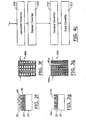
- Figure 5 illustrates an example of an array of flexible sensors 50 according to certain embodiments of the invention.
- the array 50 can be fabricated so as to provide a plurality of sensors 55.
- adjacent sensors 55 are arranged side-by-side and back-to-back or otherwise oriented to provide a high density arrangement of sensors and/or to occupy a major portion, and typically substantially all, of the surface area of the flexible array 50 .
- the term "high density” means that, when measured over at least about 0.0778 m 2 (121in 2 ) (typically in a square sheet of about 0.279x0.279 m (11x11 inches)), on average, the array 50 holds about 490 sensors 55 or at least about 4 complete sensors 55 per 0.0778 m 2 (square inch).
- the array when measured over a 0.305x0.305 m (12x12 inch) area, can hold about 750 sensors, or at least about b sensors on average.
- Figure 7 illustrates an exemplary layout of a partial sheet of an array 50' of sensors drawn to scale; the array 50' can be produced with at least 35 sensors in the vertical direction and 14 sensors in the horizontal direction (the 35x14 array shown corresponds to an 11x11 sheet).
- the 35x14 array shown corresponds to an 11x11 sheet.
- other array sizes can be used and the sensors themselves further miniaturized or enlarged, depending on the desired application.
- the sensors 55 can be symmetrically arranged in columns (the column width corresponding to the length of the sensor 551 ) and rows (with the row height corresponding to the width of the sensor 55w ), with gap spaces positioned adjacent each sensor 55 to facilitate separation from the array 50 for individual use so as to inhibit damage to the adjacent sensor upon removal.
- the array 50 can include alignment marks 59 that can facilitate the alignment of masks and system components with the metal pattern of individual sensors or groups of sensors on the array 50 during fabrication.
- the sensors 55 on the array 50 can be alternately configured, shaped, and arranged.
- the sensor length 551 can be disposed vertically on the flexible substrate 10 such that the row height corresponds to the length of the sensor or the electrode can include curvilinear traces or circular, triangulated, or other electrode shapes.
- the darkest regions correspond to locations where the laminated overlay was removed from the underlying flexible substrate, exposing either the underlying substrate or a portion of the metallic pattern 20p.
- the lighter regions correspond to locations where the laminated coverlay material 40 remains intact (sandwiching a portion of the underlying metal pattern 20p to the flexible substrate 10 ).
- the array 50 is planar and includes a metallic pattern formed on one primary surface of the underlying flexible substrate 10, each sensor 55 including a metallic pattern which defines the arrangement of at least one electrode 60e.
- the electrode 60e includes two spaced apart bond pads 60p, each having a respective connecting trace 60t, and an interdigitated array (IDA) 60i.
- the IDA can have a structure width which may be in the sub- ⁇ m range.
- the IDA 60i is positioned in the well 40w.
- Figure 6a illustrates a greatly enlarged sensor 55.
- the sensor 55 includes a well 40w having a depth "D" which corresponds to the thickness of the coverlay sheet(s) 40 laminated to the flexible substrate 40.
- Figure 6b illustrates that the well 40w can have a depth "D" corresponding to the combined thickness of two laminated coverlay sheets, 40a, 40b.
- the sheets can have the same or a different thickness and/or can be formed from the same material(s) or different material(s). For example, three sheets, each having a thickness of about 4 mils, can be used to define a well 40w with a 12 mil depth. Alternatively, a 3 mil and 2 mil sheet can be used to provide a well 40w with a 5mil depth.
- the coverlay sheet 40 can be a pre-laminated sheet of a plurality of plies of materials with or without coatings.
- the coverlay sheet(s) 40 can have a thickness of at least 0.5-10 mils (about 12-250 ⁇ m) and preferably has a thickness of about 1-20 mils (about 25-500 ⁇ m) or more.
- the wells 40 have a depth which is in the range between about 5-15mils.
- the coverlay sheet(s) 40 are selected to define a well depth "D" and perimeter shape 40s which is consistent from sensor to sensor 55 to provide a consistent testing space or volume. This can allow for improved meting of the biological fluid undergoing analysis, thus helping to provide a more consistent sample size to combine with the electrochemical formulation or solution or chemical substance(s) which may also be contained in the well 40w (not shown). In turn, reducing variation in the sensor operation can promote more reliable test results. Additional description of electrodes and analyte formulations are found in co-pending U.S. Patent Application identified by Attorney Docket No. RDC0002/US, entitled "ELECTRODES, METHODS, APPARATUSES COMPRISING MICROELECTRODE ARRAYS”.
- the well 40w can be in fluid communication with an IDA 60i or electrode 60e of a desired configuration which is in electrical communication with opposing electrical connecting traces 60t.
- the well 40w has a configuration which opens the laminated coverlay 40 to expose the underlying IDA or electrochemical active components while defining the perimeter shape 40s in a precise repeatable manner to generate a consistent reliable testing environment part to part.
- the well can be in fluid communication with a capillary segment 240c having a depth "D" (which is typically the same depth as the well) which directs fluid from the well 40w through the capillary segment 240c to the active test well 240w.
- the test well 240w may be configured to house an IDA as noted above, or other desired electrical component or electrode 60e, and/or a chemistry formulation corresponding to the test protocol for the particular sensor application.
- the sensor 55 can also include one or more electrical traces 60t and one or more bond pads 60b configured, in operation, to be electrically engageable with a testing device capable of receiving and analyzing the signal of the sensor 55 (not shown).
- the testing device can be a home unit and the sensor can be a disposable (typically, a single use disposable) sensor suitable for use by a patient, for example, to monitor glucose or other analyte levels (or the presence or absence of substances) in the blood or other body fluid or sample.
- the shape, length and configuration of the electrode or metallic pattern as the well shape, configuration or depth can vary depending on the desired end application.
- the production line can be configured to be automated and semi-continuous or continuous.
- continuous means that a production run of a desired quantity or length of material can be processed serially through each of the stations and is operated generally without substantial time delay or disruption between stations ( i.e ., certain delays are expected such as for set-up, tool change, material introduction, maintenance, queues at equipment, shift changes, planned and unplanned downtime, etc).
- short means that fabrication of the array of sensors is carried out by maintaining the product on reels of desired "continuous" lengths through selected stations.
- the reels of material are sufficient in length to have continuous production runs through at least the lamination and patterned coverlay stations (shown as stations 6-8).
- the in process or processed reels at any particular station may be queued or stored for the next workstation depending on capacity, orders, and the like. That is, for the embodiment shown, reels of flexible substrates and photoresist material as well as coverlays can be used to automatically run the processing steps in each station to form the patterned coverlay laminated to the flexible substrate and electrode surface, preferably even through any desired final curing station (shown as station 9, Figure 8i ).
- the flexible substrate 10 may be cut to form individual sheets at selected points during the process.
- the fabrication process can be automated and run in continuous lengths of material in relatively long production runs (in contrast to batch mode production operations).
- stations 2 and 6, stations 3 and 7, and/or stations 4 and 8 may be configured to be the same physical station or equipment, but configured to laminate, expose, or remove the appropriate material, depending on the desired processing step for that particular product run.
- the material is illustrated as being rerolled onto reels at the end of each workstation; however, alternatively, certain or all of the stations can be arranged to directly feed the material to the next workstation (which can be located downstream of the previous workstation) to provide direct material throughput without rolling onto reels station to station.
- the gold or metal deposited flexible substrate may be pre-fabricated or obtained from a supplier and patterned locally by the process described at workstations 2-9.
- workstation 150s corresponds to the workstation where the method step 150 of depositing gold onto the flexible substrate can be carried out).
- a roll coating station 150s conveys or pulls (or otherwise processes) the flexible substrate material 10 so as to coat a selected primary surface with the desired metal (such as gold).
- a reel of flexible substrate 10r (shown as Kapton®) is processed to include the metal (labeled as Au) on one of the primary surfaces.
- the metal coated substrate material is then rolled into a reel 110r.
- a laminating station 160s takes the material reel 110r and combines it with a photoresist film ("PR") 30 to laminate to the underlying metallized surface of the flexible substrate 10 by pressing the materials together via rollers in a hot roll-laminating machine at selected pressures and temperatures; P; T.
- PR photoresist film
- Figure 8c illustrates an exposing station 170s, where material reel 120r is unrolled and the PR 30 exposed to the ultraviolet light 38 through a mask 35 with a predetermined exposure pattern and the material is re-rolled onto a reel 120r e which now holds the exposed PR, metal, and flexible substrate.
- the material on reel 120r e is then introduced to a developing station 180s, as shown in Figure 8d where the PR is developed, rinsed and dried, resulting in a composition of patterned PR on metal and flexible substrate which can be rolled onto a reel 125r.
- the material on reel 125r can then be introduced to an etching station 190s where the metal can be etched, the PR stripped, and the patterned metal 20p on flexible substrate 10 dried and rolled onto reel 126r.
- Figure 8f illustrates a coverlay application station 200s, where the coverlay sheet 40 can be introduced as a substantially continuous reel of material 40r and the flexible substrate with the metallic pattern can also be introduced as a continuous reel of material.
- the continuous lengths of materials can be forced together so that the coverlay sheet 40 is secured to the underlying materials.
- the coverlay sheet is laminated or united to the patterned metal surface 20p and the underlying flexible substrate in a hot roll lamination machine which presses the two materials together (which may be evacuated during the procedure to reduce the likelihood that air is trapped between the layers).
- the laminated coverlay 40, metal pattern 20p, and flexible substrate 10 can then be rolled onto a reel 127r.
- step 6 can be repeated as desired to laminate additional coverlay material sheets onto the first laminated coverlay surface.
- Figure 8g illustrates a coverlay exposure station 205s, where the laminated coverlay material 127r is exposed to a light source (similar to the photoresist material processed at station 3) and collected and rolled to form a reel 127r e of exposed coverlay material on patterned metal 20p and flexible substrate 10.
- the reel exposed coverlay material 127r e is then taken to developing station 210s ( Figure 8h ), where the coverlay material 40 is developed to yield a laminated patterned coverlay layer 40p overlying a patterned metal surface 20p on the flexible substrate 10 which can be collected on a reel 128r.
- the reel of material 128r can then be directed to travel through a thermal curing station 205s to cure the coverlay material 40 (for example, an oven at about 160°C with a conveying tension and speed set so that the coverlay sheet is cured for about 1 hour).
- a thermal curing station 205s to cure the coverlay material 40 (for example, an oven at about 160°C with a conveying tension and speed set so that the coverlay sheet is cured for about 1 hour).
- a more complex array continuous travel pattern (not shown) can be used to occupy more of the space in the oven (i.e ., spiral or zig-zag to use more vertical space).
- the array 50 can be cut into desired lengths and conveyed through the oven. As shown, the continuous length of array 50 is rolled onto a finished array material spool or reel 129r which can be transported to a pharmaceutical location where a desired chemical formulation can be added to the wells and the sensors split into individual units.
- an additional coverlay layer or layers can be positioned to define a ceiling or lid over the underlying laminated coverlay defining the well(s) (not shown).
- the ceiling coverlay layer can be configured to enclose the underlying surface or portions of the surface such as to enclose the well.
- the enclosed well configuration may be particularly suitable for enclosed microfluidic testing environments.
- the ceiling coverlay layer may be patterned to define a port or openings in the ceiling layer to allow electrical or fluid access to desired regions thereunder.
- a port can be patterned into the ceiling coverlay to allow fluid passage to a portion of the well.
- the fluid travel passage can be provided through vias or passages formed up through the substrate layer or formed laterally through an intermediate layer (such as, when viewed from the top, a lateral passage extending from an open end region to the testing well).
- an additional ceiling forming set of stations (similar to those used to form the coverlay(s) defining the wells onto the substrate can be used to laminate the ceiling coverlay to the underlying structure and/or pattern the ceiling coverlay as desired.
- a gold film or layer is deposited onto a flexible substrate formed of 7 mil thick Kaladex® film using a planar DC magnetron sputtering process and equipment operated Techni-Met Inc. (a roll coating company), located in Windsor, CT.
- the thickness of the gold film can range from 30 to 200 nm, with a preferred thickness being about 100nm.
- Seed layers of chromium or titanium can be sputtered between the substrate film and the gold layers to promote better adhesion of the gold to the substrate film; however, gold layers sputtered directly onto the substrate film without such seeding can exhibit sufficient adhesion. Plasma treatment of substrate surface can improve the adhesion of gold.
- a dry film photopolymer resist was laminated to the gold/substrate film.
- a dry film resist such as that sold under the trademark Riston® CM206 (duPont) was used.
- the Riston® CM206 photoresist was first wet laminated onto the gold surface of 12" x 12" gold/substrate panels using a HRL-24 hot roll laminator (from duPont). The sealing temperature and lamination speed were about 105°C and 1 meter per minute, respectively.
- the laminated panel was placed in a Tamarack model 152R exposure system, from Tamarack Scientific Co., Inc., Anaheim, CA. The release liner was removed from the top surface of the photoresist.
- a glass/Cr photomask was produced by Advance Reproductions Corporation, North Andover, MA.
- the Cr side of the mask was treated with an antistick coating (Premitech Inc., Raleigh, NC), and was placed directly onto the photoresist surface of the panel.
- the laminated panel was exposed to ultraviolet light of 365 nm through the photomask using an exposure energy of 60 mJ/cm 2 .
- Unexposed photoresist was stripped from the panel in a rotary vertical lab processor (VLP-20), Circuit Chemistry Equipment, Golden Valley, MN, using 1% potassium carbonate, at room temperature, for 30 seconds using a nozzle pressure of 34 psi.
- Exposed gold on the sheet was then stripped using an etch bath containing a solution of 4 parts I 2 :1 par KI:40 parts water vol./vol.; and 0.04 gram FluoradTM fluorochemical surfactant FC99, (3M, St. Paul, MN) per 100 gram solution, added to the bath to ensure wetting of the gold. Air was bubbled through the bath during the etch process to obtain a sufficiently uniform agitation of the bath mixture. The panel was rinsed with deionized water and residual Riston® CM206 was removed in a 3% KOH bath.
- Articles were fabricated using dry film photoimageable coverlay materials such as that sold under the trademark Vacrel® 8140 (and related series) from duPont or Pyralux® PC series (duPont).
- the chamber dimensions can be accurately defined by flex circuit photolithography. Depth of the chamber was controlled by the thickness of the coverlay materials used and/or whether single or multiple layers of the coverlay dry film were used. Chamber depth was achieved by sequential lamination of different coverlay materials as follows: four mil thick Vacrel® 8130 was first laminated to the electrode side of the substrate using a HRL024 (duPont) heated roll laminator at room temperature, using a roller speed of 1 meter per minute.
- HRL024 duePont
- the electrode panel was then vacuum laminated in a DVL-24 vacuum laminator (duPont) using settings of 120°F, 30 second vacuum dwell, and a 4 second pressure dwell to remove entrapped air between the coverlay film and the electrode substrate.
- Two mil thick Vacrel® 8120 was laminated next to the Vacrel® 8130 surface using the HRL-24 at room temperature, with a roller speed of 1 meter/min.
- the panel was then vacuum laminated again in the DVL-24 vacuum laminator using a 30 second vacuum dwell, 4 second pressure, to remove entrapped air between the two coverlay films.
- the laminated electrode sheet was placed in the Tamarack 152R system and was exposed to ultraviolet light at 365 nm through the photomask for 22 seconds using an exposure intensity of 17 mW/cm 2 .
- the unexposed coverlay was stripped from the panel using the VLP-20 Circuit Chemistry Equipment) in 1% K 2 CO 3 , at 140°F, for 75 seconds using a nozzle pressure of 34 psi.
- the developed laminate structure was rinsed in deionized water, and then cured at 160°C for 1 hour to thermally crosslink the coverlay material.
Abstract
Description
- Work related to the invention was sponsored by the NSF CECT under Grant No. CDR-8622201. The United States Government has certain rights to this invention.
- This application claims priority to
U.S. Provisional Application Serial Number 60/332,194, filed November 16, 2001 - The present invention relates to methods for fabricating electrochemical sensors or wells on flexible substrates and associated products. The products may be particularly suitable for use as disposable biomedical sensors.
- Probes or sensors used in medical diagnostic or evaluation procedures often use electrochemical detection provided by dry or fluid/liquid chemistries/electrolytes placed on top of electrodes formed of precious metals (gold, platinum, etc). The probes or sensors can employ chemistries/electrolytes such as solid potassium chloride (such as for reference electrodes) or other chemicals, hydrogels (sometimes containing an internal electrolyte underneath the membrane of an ion-sensitive electrode), or enzyme-containing material. The sensors or probes also typically employ wells or small pools, some of which can be configured to act as capillary spaces to guide quantities of a sample solution (such as blood) to and/or from the electrodes on the probe or sensor.
- For many of these applications, the wells are patterned into materials which are selected so that they are compatible with flexible substrates such as polyimide films (Kapton®, Upilex®, and the like). In the past, thin film processing techniques have had problems generating coatings thick enough for proper well formation in chemical sensor applications. In addition, screen printed materials used with thick film processing techniques may be either incompatible with flexible materials or inhibit the formation of fine line resolution desired for small or miniaturized electrodes.
- Cosofret et al., in Microfabricated Sensor Arrays Sensitive to pH and K+ for Ionic Distribution Measurements in the Beating Heart, 67 Anal. Chem., pp. 1647-1653 (1995), described spin-coating a polyimide layer of about 30µm onto a film or substrate. Unfortunately, spin-coating methods can, as a practical matter, limit the well depth and/or precise boundary or perimeter definition during formation. In addition, spin-coating methods may be limited to batch fabrication processes and are generally not commercially compatible with high volume, low-cost (continuous or semi-continuous) mass production methods. In view of the foregoing, there is a need for improved, economic ways to fabricate wells and microenvironments for electrochemical sensors on flexible substrates.
- The present invention is directed to a flexible sensor according to
claim 1 and to a method for fabricating a sensor according toclaim 10. - In certain embodiments, the present invention is directed to methods for fabricating a plurality of sensors on a flexible substrate, each sensor having at least one associated electrode and at least one well. As used herein, the term "well" means a reservoir or chamber used to receive or hold a quantity of fluid therein (typically sized and configured as a microfluidic environment). As such, the term "well" includes at least one discrete chamber or a plurality of chambers (in fluid communication or in fluid isolation, as the application desires) and can alternatively or additionally include one or more channels (linear or other desired complex or irregular shapes (such as spiral, annular, etc.)), or combinations of a well(s) and channel(s).
- In certain embodiments, the method includes: (a) providing a flexible substrate material layer having a surface area defined by a length and width thereof; (b) forming a plurality of sensors onto the flexible substrate material layer, each sensor comprising a predetermined metallic pattern defining at least one electrode; (c) disposing at least one coverlay sheet over the flexible substrate sandwiching the sensors therebetween, the coverlay sheet having an associated thickness; (d) laminating the at least one coverlay sheet to the flexible substrate layer; and (e) removing predetermined regions of the laminated coverlay sheet from the flexible substrate layer to define a well (which may be or include a channel) with a depth corresponding to the thickness of the coverlay sheet.
- In certain embodiments, the removing step also exposes a portion of the underlying metallic pattern of each sensor (such as bond pads and an interdigitated array or "IDA"). The array of sensors can be arranged such that the sensors are aligned back to back and side by side to occupy a major portion of the surface area of the flexible substrate. In addition, the patterned coverlay can be configured such that the well is a microfluidic channel or a channel with a well. In certain embodiments, the assembly may be configured such that there are openings in the coverlay for bond pads and the like to make any desired electrical connection(s).
- Other embodiments of the invention are directed to arrays of flexible sensors. The arrays of flexible sensors include: (a) a flexible substrate layer having opposing primary surfaces, (b) an electrode layer disposed as a repetition of metallic electrically conductive patterns on one of the primary surfaces of the substrate layer, the metallic pattern corresponding to a desired electrode arrangement for a respective sensor; and (c) a first coverlay sheet layer having a thickness overlying and laminated to the first flexible substrate layer to sandwich the electrode layer therebetween. The third coverlay sheet layer has a plurality of apertures formed therein. The apertures define a well for each of the sensors on the flexible substrate. The wells have a depth corresponding to the thickness of the coverlay sheet layer.
- Other embodiments are directed to flexible sensors, which can be single use or disposable bioactive sensors. Similar to the array of sensors, the individual sensors can be multi-layer laminated structures including: (a) a flexible substrate layer; (b) an electrode layer comprising a conductive pattern of material disposed onto one of the primary surfaces of the first flexible substrate layer; and (c) a first flexible coverlay layer overlying the electrode layer and laminated to the electrode layer and the substrate layer, wherein the first flexible coverlay layer has a well formed therein, the well having a depth of at least about 1-10 mils (.001-.01 inches) or, in a metric system, at least about 25-250 µm. Of course greater well depths can also be generated, such as by using thicker coverlay sheets or combinations of sheets, to yield well depths of about 12 mils (about 300 µm) or more, depending on the application.
- In certain embodiments, the array of sensors or each sensor can include a second coverlay layer having a thickness of between about 1-10mils overlying and secured to the first coverlay layer. The second coverlay layer also has a plurality of apertures formed therein, the apertures corresponding to the apertures in the first coverlay layer. Thus, the wells have a depth corresponding to the combined thickness of the first and second coverlay layers. In other embodiments, a third coverlay layer can also be employed by laminating it to the second coverlay layer and removing the material overlying the well site to provide a well depth corresponding to the thickness of the first, second, and third coverlay layers.
- The method of fabricating the sensor arrays can be carried out in an automated continuous production run that increases the production capacity over batch type processes. In addition, the wells can be formed with increased volume, capacity, or depth over conventional microfabrication techniques. The method can be performed such that the sensors are arranged on the flexible substrate in a high-density pattern of at least about 4 sensors per square inch when measured over about 122 square inches. In other high-density embodiments, for a sheet which is 12 inches by 12 inches (144 square inches), about 750 sensors can be arranged thereon, averaging at least about 5 sensors per square inch. In certain embodiments, the sensors and arrays are configured to be heat resistant or to withstand sterilization procedures suitable for biomedical products.
- The coverlay material is a photosensitive dry film material. Examples of suitable coverlay materials include photoimageable polymers, acrylics, and derivatives thereof including, but not limited to, commercially available PYRALUX® PC and VACREL® from DuPont, and CONFORMASK® from Morton. In addition, the coverlay sheet may be a pre-laminated sheet of a plurality of plies of one or more types and/or varying thickness of dry film coverlay materials and may also include desired coatings.
- The foregoing and other objects and aspects of the present invention are explained in detail in the specification set forth below.
-
-
Figure 1 is a flow chart of method steps for fabricating sensors with wells on a flexible substrate according to embodiments of the present invention. -
Figures 2a-2g are side views of a fabrication sequence of flexible substrate sensors using coverlay sheet material according to embodiments of the present invention. -
Figures 3a-3g are top views of the sequence shown inFigures 2a-2g , (withFigures 2a and 3a correspond to one another,Figures 2b and 3b corresponding to one another and so on. -
Figure 4 is a flow chart of the sequence of fabrication steps illustrated inFigures 2 and 3 . -
Figure 5 is a photocopy of the upper surface of a partial sheet of an array of sensors with wells on a flexible substrate according to embodiments of the present invention. -
Figure 6a is a greatly enlarged side perspective view of a sensor with a well according to embodiments of the present invention. -
Figure 6b is a greatly enlarged side perspective view of a sensor with a well having a depth corresponding to the combined thickness of multiple coverlayer sheets. -
Figure 7 is a top view of a partial sheet of an array of sensors drawn to scale according to embodiments of the present invention. -
Figures 8a-8i are schematic illustrations of stations in a production line for fabricating arrays of flexible sensors according to embodiments of the present invention. - The present invention will now be described more fully hereinafter with reference to the accompanying figures, in which preferred embodiments of the invention are shown. This invention may, however, be embodied in many different forms and should not be construed as limited to the embodiments set forth herein. Like numbers refer to like elements throughout. In the figures, layers, components, or features may be exaggerated for clarity.
- In certain embodiments, as shown in
Figure 1 , steps for fabricating a flexible sensor can include first providing a flexible substrate material layer (Block 100). The flexible substrate material layer can be an elastomeric film such as polyimide films. Examples of commercially available films include, but are not limited to, Kapton®, Upilex®, Kaladex® and the like. Next, a plurality of sensors can be formed on the flexible substrate layer via depositing or forming a desired conductive and/or metallic electrode pattern thereon (Block 110). Any suitable metal trace fabrication technique may be employed, such as sputtering or deposition of the metal followed by photolithography or laser ablation, stenciling, screen-printing, shadow masking, and the like. - In any event, after the metallic pattern is formed on the substrate, at least one coverlay sheet layer having an associated thickness can then be disposed to overlie the flexible substrate layer so as to sandwich the sensors or metallic pattern therebetween (Block 120). The coverlay sheet can be a photosensitive and/or photoimageable coverlay dry film material. Examples of suitable coverlay materials include photoimageable polymers, acrylics, flexible composites, and derivatives thereof including, but not limited to, commercially available PYRALUX® PC and VAGREL® from DuPont, and CONFORMASK® from Morton. In addition, the coverlay sheet may be a pre-laminated sheet of a plurality of plies of one or more types and/or varying thickness of dry film coverlay materials and may also include desired coatings. The coverlay material maybe selected so as to be heat resistant or compatible with irradiation sterilization procedures as, in use, the sensor may be exposed to sterilization procedures, particularly for biomedical applications.
- The coverlay sheet is laminated to the underlying flexible substrate layer (i.e., the layers are united) (Block 130). The layers can be united by hot roll lamination techniques, or other suitable lamination means suitable to unite the layers together. Predetermined regions of the laminated coverlay sheet can be removed from the flexible substrate layer to define a well with a depth corresponding to the thickness of the coverlay sheet layer (Block 140). In certain embodiments, two or more coverlay sheets can be laminated, serially, onto the flexible substrate to define a well with a depth corresponding to the combined thickness of the coverlay sheets used.
-
Figures 2 and 3 illustrate a sequence of operations, suitable for certain embodiments, which can be used to form a flexible sensor array (which can be separated to form individual disposable sensors as will be discussed further below). As shown inFigure 2a and 3a , first aconductive metal 20 can be deposited onto the flexible substrate layer 10 (Block 150,Figure 4 ). Theconductive metal 20 can be any suitable conductor as is well known to those of skill in the art, including, but not limited to, gold, silver, platinum, palladium, titanium, chromium and mixtures thereof. In certain embodiments, themetal 20 can be formed as a relatively thin layer of about 30-200nm, and is typically about 100nm. Themetal 20 can be applied via a sputtering process. A suitable metal coated flexible substrate material is available from Techni-Met, Inc., located in Windsor, CT. Additional additives such as adhesive enhancing materials (such as seed layers of chromium or titanium) can be sputtered or sprayed or otherwise deposited onto thesubstrate 10 to promote the adhesion of themetal 20 to thesubstrate layer 10. - As shown in
Figures 2b and 3b , a dry filmphotoresist material layer 30 can be laminated onto the metal layer 20 (Figure 4 , Block 160). Thephotoresist material 30 can be a dry film resist such as Riston® CM206 from DuPont Industries. Thephotoresist material 30 may be wet laminated by hot rolling the photoresist onto the metal coatedsurface 20 of the substrate using a HRL-24 hot roll laminator (also available from DuPont). Subsequently, as shown inFigure 2c , aphotomask 35 with a predetermined mask pattern is positioned between thephotoresist material 30 and an ultraviolet light source and theultraviolet light 38 travels through desired apertures in themask 35 to expose photoresist material about the unmaskedregions 39e but not themasked regions 39u, thereby forming a desired exposure pattern in the laminated dryfilm photoresist material 30. Thus, predetermined regions of the photoresist material are exposed (Figure 4 , Block 170). In the embodiment shown, a negative photoprocessing system is employed, the mask being configured to cover the regions (and prevent exposure) which will define the desired trace or electrode pattern. However, a positive imaging or photoprocessing technique can also be used as is well known to those of skill in the art. - As shown in
Figures 2d and 3d , thephotoresist material 30 is then developed (Figure 4 , Block 180), leaving the patternedphotoresist 39p on the surface (the exposed regions being removed).Figures 2e and 3e illustrate that next the metal pattern is etched into themetal layer 20 corresponding to the laminated photoresist material remaining thereon (Figure 4 , Block 190). As shown inFigures 2e and 3e , after themetal pattern 20p is formed, the remainder of thephotoresist material 30 is removed or stripped (Figure 4 , Block 195), leaving thesubstrate layer 20 with the desiredmetallic pattern 20p thereon. - Next, as shown in
Figures 2f and 3f (andFigure 4 ,Blocks 200, 205), acoverlay material 40 is laminated onto theflexible substrate 10 sandwiching themetallic pattern 20p therebetween. The lamination can be performed as a hot roll process, which presses the two layers together. The lamination can be carried out under vacuum to help remove air which may be trapped or residing between the two joining surfaces. - As before,
Figures 2f and 3f illustrate that photolithography can be used to expose desiredregions 40e of thecoverlay material 40, which is then selectively removed (or if desired, the reverse processing can be used, i.e., the unexposed material can be removed) thereby forming the desired pattern in thecoverlay material 40p, which then forms the well and/or exposes theunderlying metal 20 orsubstrate material 10. The exposed material is removed about a well region formed by the selective removal of thecoverlay material 40, thewell 40w having a depth corresponding to the thickness of the coverlay. As shown inFigure 2f , amask 45 is positioned between an ultraviolet light source and the light rays travel through openings in themask 45 to expose the predetermined regions in thecoverlay material 40. The coverlay material is then developed (Figure 4 , Block 210) and theunwanted coverlay material 40 is removed or stripped, leaving a flexible array of sensors with surface regions exposed to the underlying material (either theflexible substrate 10, or the metal layer 20). The coverlay material can then be cured (Figure 4 , Block 215). Any suitable curing technique can be employed, but typically a thermal curing process is employed to heat the coverlay material to desired temperatures and for desired cure times to thermally cross-link the coverlay material. Doing so "permanently secures" the coverlay material(s) to the underlying substrate and/or to inhibit the degradation or separation of the structure in use (maintaining the integrity of the attachment between the coverlay material and the underlying materials). Other curing means may be used, as suitable, depending on the materials employed, including, but not limited to, oven or other heat source, microwave, RF, or ultrasound energy, and/or laser, ultraviolet light or other light source. -
Figure 5 illustrates an example of an array offlexible sensors 50 according to certain embodiments of the invention. As shown, thearray 50 can be fabricated so as to provide a plurality ofsensors 55. In certain embodiments,adjacent sensors 55 are arranged side-by-side and back-to-back or otherwise oriented to provide a high density arrangement of sensors and/or to occupy a major portion, and typically substantially all, of the surface area of theflexible array 50. The term "high density" means that, when measured over at least about 0.0778 m2 (121in2) (typically in a square sheet of about 0.279x0.279 m (11x11 inches)), on average, thearray 50 holds about 490sensors 55 or at least about 4complete sensors 55 per 0.0778 m2 (square inch). In certain embodiments, when measured over a 0.305x0.305 m (12x12 inch) area, the array can hold about 750 sensors, or at least about b sensors on average.Figure 7 illustrates an exemplary layout of a partial sheet of an array 50' of sensors drawn to scale; the array 50' can be produced with at least 35 sensors in the vertical direction and 14 sensors in the horizontal direction (the 35x14 array shown corresponds to an 11x11 sheet). Of course, other array sizes can be used and the sensors themselves further miniaturized or enlarged, depending on the desired application. - As shown in
Figure 5 , thesensors 55 can be symmetrically arranged in columns (the column width corresponding to the length of the sensor 551) and rows (with the row height corresponding to the width of thesensor 55w), with gap spaces positioned adjacent eachsensor 55 to facilitate separation from thearray 50 for individual use so as to inhibit damage to the adjacent sensor upon removal. Thearray 50 can include alignment marks 59 that can facilitate the alignment of masks and system components with the metal pattern of individual sensors or groups of sensors on thearray 50 during fabrication. - It is noted that the
sensors 55 on the array 50 (including the depth of thewell 40w andmetal pattern 20p which defines the desired electrical or electrode arrangement) can be alternately configured, shaped, and arranged. For example, thesensor length 551 can be disposed vertically on theflexible substrate 10 such that the row height corresponds to the length of the sensor or the electrode can include curvilinear traces or circular, triangulated, or other electrode shapes. InFigure 5 and7 , the darkest regions correspond to locations where the laminated overlay was removed from the underlying flexible substrate, exposing either the underlying substrate or a portion of themetallic pattern 20p. The lighter regions correspond to locations where thelaminated coverlay material 40 remains intact (sandwiching a portion of theunderlying metal pattern 20p to the flexible substrate 10). - As shown in
Figure 5 , thearray 50 is planar and includes a metallic pattern formed on one primary surface of the underlyingflexible substrate 10, eachsensor 55 including a metallic pattern which defines the arrangement of at least oneelectrode 60e. In the embodiment shown inFigures 5-7 , theelectrode 60e includes two spaced apartbond pads 60p, each having a respective connectingtrace 60t, and an interdigitated array (IDA) 60i. In certain embodiments, the IDA can have a structure width which may be in the sub-µm range. In the embodiment shown, theIDA 60i is positioned in thewell 40w. For additional information on IDA's, see, e.g.,U.S. Patent No. 5,670,031 andWO 97/34140 -
Figure 6a illustrates a greatlyenlarged sensor 55. As shown, thesensor 55 includes awell 40w having a depth "D" which corresponds to the thickness of the coverlay sheet(s) 40 laminated to theflexible substrate 40.Figure 6b illustrates that thewell 40w can have a depth "D" corresponding to the combined thickness of two laminated coverlay sheets, 40a, 40b. As noted above, one, two, or three ormore sheets 40 can be used to generate the desired well depth. The sheets (shown inFigure 6b as 40a, 40b) can have the same or a different thickness and/or can be formed from the same material(s) or different material(s). For example, three sheets, each having a thickness of about 4 mils, can be used to define awell 40w with a 12 mil depth. Alternatively, a 3 mil and 2 mil sheet can be used to provide awell 40w with a 5mil depth. - As also noted above, the
coverlay sheet 40 can be a pre-laminated sheet of a plurality of plies of materials with or without coatings. In addition, as also noted above, the coverlay sheet(s) 40 can have a thickness of at least 0.5-10 mils (about 12-250 µm) and preferably has a thickness of about 1-20 mils (about 25-500 µm) or more. In certain embodiments, thewells 40 have a depth which is in the range between about 5-15mils. - In certain embodiments, the coverlay sheet(s) 40 are selected to define a well depth "D" and
perimeter shape 40s which is consistent from sensor tosensor 55 to provide a consistent testing space or volume. This can allow for improved meting of the biological fluid undergoing analysis, thus helping to provide a more consistent sample size to combine with the electrochemical formulation or solution or chemical substance(s) which may also be contained in thewell 40w (not shown). In turn, reducing variation in the sensor operation can promote more reliable test results. Additional description of electrodes and analyte formulations are found in co-pending U.S. Patent Application identified by Attorney Docket No. RDC0002/US, entitled "ELECTRODES, METHODS, APPARATUSES COMPRISING MICROELECTRODE ARRAYS". - As shown in
Figure 6a , thewell 40w can be in fluid communication with anIDA 60i orelectrode 60e of a desired configuration which is in electrical communication with opposing electrical connectingtraces 60t. Typically, thewell 40w has a configuration which opens thelaminated coverlay 40 to expose the underlying IDA or electrochemical active components while defining theperimeter shape 40s in a precise repeatable manner to generate a consistent reliable testing environment part to part. - As shown in
Figure 6b , the well can be in fluid communication with acapillary segment 240c having a depth "D" (which is typically the same depth as the well) which directs fluid from thewell 40w through thecapillary segment 240c to the active test well 240w. The test well 240w may be configured to house an IDA as noted above, or other desired electrical component orelectrode 60e, and/or a chemistry formulation corresponding to the test protocol for the particular sensor application. Thesensor 55 can also include one or moreelectrical traces 60t and one ormore bond pads 60b configured, in operation, to be electrically engageable with a testing device capable of receiving and analyzing the signal of the sensor 55 (not shown). - In certain embodiments, the testing device can be a home unit and the sensor can be a disposable (typically, a single use disposable) sensor suitable for use by a patient, for example, to monitor glucose or other analyte levels (or the presence or absence of substances) in the blood or other body fluid or sample. It will be appreciated that the shape, length and configuration of the electrode or metallic pattern as the well shape, configuration or depth can vary depending on the desired end application.
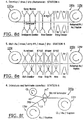
- Turning now to
Figures 8a-8i , an exemplary embodiment of a production line with nine production workstations is shown. In certain embodiments, the production line can be configured to be automated and semi-continuous or continuous. The word "continuous" means that a production run of a desired quantity or length of material can be processed serially through each of the stations and is operated generally without substantial time delay or disruption between stations (i.e., certain delays are expected such as for set-up, tool change, material introduction, maintenance, queues at equipment, shift changes, planned and unplanned downtime, etc). The term "semi-continuous" as used herein, means that fabrication of the array of sensors is carried out by maintaining the product on reels of desired "continuous" lengths through selected stations. Typically, the reels of material are sufficient in length to have continuous production runs through at least the lamination and patterned coverlay stations (shown as stations 6-8). Of course, the in process or processed reels at any particular station may be queued or stored for the next workstation depending on capacity, orders, and the like. That is, for the embodiment shown, reels of flexible substrates and photoresist material as well as coverlays can be used to automatically run the processing steps in each station to form the patterned coverlay laminated to the flexible substrate and electrode surface, preferably even through any desired final curing station (shown asstation 9,Figure 8i ). In addition, theflexible substrate 10 may be cut to form individual sheets at selected points during the process. However, by using reels of arrays or materials, the fabrication process can be automated and run in continuous lengths of material in relatively long production runs (in contrast to batch mode production operations). - Although shown as nine separate workstations in
Figures 8a-8i , for ease of discussion, it is noted that some of the stations can be multipurpose or combined with other workstations. For example, one or more ofstations stations stations - For clarity, the workstations have been identified with feature numbers which correspond to the method steps shown in
Figure 4 (i.e.,workstation 150s corresponds to the workstation where themethod step 150 of depositing gold onto the flexible substrate can be carried out). - Turning now to
Figure 8a , as shown, aroll coating station 150s conveys or pulls (or otherwise processes) theflexible substrate material 10 so as to coat a selected primary surface with the desired metal (such as gold). As shown, a reel offlexible substrate 10r (shown as Kapton®) is processed to include the metal (labeled as Au) on one of the primary surfaces. The metal coated substrate material is then rolled into areel 110r. As shown inFigure 8b , alaminating station 160s, takes thematerial reel 110r and combines it with a photoresist film ("PR") 30 to laminate to the underlying metallized surface of theflexible substrate 10 by pressing the materials together via rollers in a hot roll-laminating machine at selected pressures and temperatures; P; T. Thelaminated photoresist 30,metal 20, andflexible substrate 10 are then rolled ontoreel 120r. -
Figure 8c illustrates an exposingstation 170s, wherematerial reel 120r is unrolled and thePR 30 exposed to theultraviolet light 38 through amask 35 with a predetermined exposure pattern and the material is re-rolled onto areel 120re which now holds the exposed PR, metal, and flexible substrate. The material onreel 120re is then introduced to a developingstation 180s, as shown inFigure 8d where the PR is developed, rinsed and dried, resulting in a composition of patterned PR on metal and flexible substrate which can be rolled onto areel 125r. As shown inFigure 8e , the material onreel 125r can then be introduced to anetching station 190s where the metal can be etched, the PR stripped, and the patternedmetal 20p onflexible substrate 10 dried and rolled ontoreel 126r. -
Figure 8f illustrates acoverlay application station 200s, where thecoverlay sheet 40 can be introduced as a substantially continuous reel of material 40r and the flexible substrate with the metallic pattern can also be introduced as a continuous reel of material. The continuous lengths of materials can be forced together so that thecoverlay sheet 40 is secured to the underlying materials. As shown, the coverlay sheet is laminated or united to the patternedmetal surface 20p and the underlying flexible substrate in a hot roll lamination machine which presses the two materials together (which may be evacuated during the procedure to reduce the likelihood that air is trapped between the layers). Thelaminated coverlay 40,metal pattern 20p, andflexible substrate 10 can then be rolled onto areel 127r. Although not shown,step 6 can be repeated as desired to laminate additional coverlay material sheets onto the first laminated coverlay surface. -
Figure 8g illustrates a coverlay exposure station 205s, where thelaminated coverlay material 127r is exposed to a light source (similar to the photoresist material processed at station 3) and collected and rolled to form areel 127re of exposed coverlay material on patternedmetal 20p andflexible substrate 10. The reel exposedcoverlay material 127re is then taken to developingstation 210s (Figure 8h ), where thecoverlay material 40 is developed to yield a laminated patternedcoverlay layer 40p overlying a patternedmetal surface 20p on theflexible substrate 10 which can be collected on areel 128r. The reel ofmaterial 128r can then be directed to travel through a thermal curing station 205s to cure the coverlay material 40 (for example, an oven at about 160°C with a conveying tension and speed set so that the coverlay sheet is cured for about 1 hour). Of course, other temperatures and times (and related conveyor speeds can also be used). In addition, a more complex array continuous travel pattern (not shown) can be used to occupy more of the space in the oven (i.e., spiral or zig-zag to use more vertical space). Alternatively, thearray 50 can be cut into desired lengths and conveyed through the oven. As shown, the continuous length ofarray 50 is rolled onto a finished array material spool or reel 129r which can be transported to a pharmaceutical location where a desired chemical formulation can be added to the wells and the sensors split into individual units. - It is also noted that, in certain embodiments, an additional coverlay layer or layers can be positioned to define a ceiling or lid over the underlying laminated coverlay defining the well(s) (not shown). The ceiling coverlay layer can be configured to enclose the underlying surface or portions of the surface such as to enclose the well. The enclosed well configuration may be particularly suitable for enclosed microfluidic testing environments. The ceiling coverlay layer may be patterned to define a port or openings in the ceiling layer to allow electrical or fluid access to desired regions thereunder. In certain embodiments, a port can be patterned into the ceiling coverlay to allow fluid passage to a portion of the well. In other embodiments using enclosed well (chamber and/or channel) configurations, the fluid travel passage can be provided through vias or passages formed up through the substrate layer or formed laterally through an intermediate layer (such as, when viewed from the top, a lateral passage extending from an open end region to the testing well). In these embodiments, an additional ceiling forming set of stations (similar to those used to form the coverlay(s) defining the wells onto the substrate can be used to laminate the ceiling coverlay to the underlying structure and/or pattern the ceiling coverlay as desired.
- The invention is explained in greater detail in the following non-limiting examples.
- The following process was used to prepare an article according to embodiments of the invention. According to the method, a gold film or layer is deposited onto a flexible substrate formed of 7 mil thick Kaladex® film using a planar DC magnetron sputtering process and equipment operated Techni-Met Inc. (a roll coating company), located in Windsor, CT. The thickness of the gold film can range from 30 to 200 nm, with a preferred thickness being about 100nm. Seed layers of chromium or titanium can be sputtered between the substrate film and the gold layers to promote better adhesion of the gold to the substrate film; however, gold layers sputtered directly onto the substrate film without such seeding can exhibit sufficient adhesion. Plasma treatment of substrate surface can improve the adhesion of gold.
- After the gold was applied to the flexible substrate, a dry film photopolymer resist was laminated to the gold/substrate film. A dry film resist such as that sold under the trademark Riston® CM206 (duPont) was used. The Riston® CM206 photoresist was first wet laminated onto the gold surface of 12" x 12" gold/substrate panels using a HRL-24 hot roll laminator (from duPont). The sealing temperature and lamination speed were about 105°C and 1 meter per minute, respectively. The laminated panel was placed in a Tamarack model 152R exposure system, from Tamarack Scientific Co., Inc., Anaheim, CA. The release liner was removed from the top surface of the photoresist. A glass/Cr photomask was produced by Advance Reproductions Corporation, North Andover, MA. The Cr side of the mask was treated with an antistick coating (Premitech Inc., Raleigh, NC), and was placed directly onto the photoresist surface of the panel. The laminated panel was exposed to ultraviolet light of 365 nm through the photomask using an exposure energy of 60 mJ/cm2. Unexposed photoresist was stripped from the panel in a rotary vertical lab processor (VLP-20), Circuit Chemistry Equipment, Golden Valley, MN, using 1% potassium carbonate, at room temperature, for 30 seconds using a nozzle pressure of 34 psi. Exposed gold on the sheet was then stripped using an etch bath containing a solution of 4 parts I2:1 par KI:40 parts water vol./vol.; and 0.04 gram Fluorad™ fluorochemical surfactant FC99, (3M, St. Paul, MN) per 100 gram solution, added to the bath to ensure wetting of the gold. Air was bubbled through the bath during the etch process to obtain a sufficiently uniform agitation of the bath mixture. The panel was rinsed with deionized water and residual Riston® CM206 was removed in a 3% KOH bath.
- Articles were fabricated using dry film photoimageable coverlay materials such as that sold under the trademark Vacrel® 8140 (and related series) from duPont or Pyralux® PC series (duPont). The chamber dimensions can be accurately defined by flex circuit photolithography. Depth of the chamber was controlled by the thickness of the coverlay materials used and/or whether single or multiple layers of the coverlay dry film were used. Chamber depth was achieved by sequential lamination of different coverlay materials as follows: four mil thick Vacrel® 8130 was first laminated to the electrode side of the substrate using a HRL024 (duPont) heated roll laminator at room temperature, using a roller speed of 1 meter per minute. The electrode panel was then vacuum laminated in a DVL-24 vacuum laminator (duPont) using settings of 120°F, 30 second vacuum dwell, and a 4 second pressure dwell to remove entrapped air between the coverlay film and the electrode substrate. Two mil thick Vacrel® 8120 was laminated next to the Vacrel® 8130 surface using the HRL-24 at room temperature, with a roller speed of 1 meter/min. The panel was then vacuum laminated again in the DVL-24 vacuum laminator using a 30 second vacuum dwell, 4 second pressure, to remove entrapped air between the two coverlay films.
- The laminated electrode sheet was placed in the Tamarack 152R system and was exposed to ultraviolet light at 365 nm through the photomask for 22 seconds using an exposure intensity of 17 mW/cm2. The unexposed coverlay was stripped from the panel using the VLP-20 Circuit Chemistry Equipment) in 1% K2CO3, at 140°F, for 75 seconds using a nozzle pressure of 34 psi. The developed laminate structure was rinsed in deionized water, and then cured at 160°C for 1 hour to thermally crosslink the coverlay material.
- The foregoing is illustrative of the present invention and is not to be construed as limiting thereof. Although a few exemplary embodiments of this invention have been described, those skilled in the art will readily appreciate that many modifications are possible in the exemplary embodiments without materially departing from the novel teachings and advantages of this invention. Accordingly, all such modifications are intended to be included within the scope of this invention as defined in the claims. In the claims, means-plus-function clauses, where used, are intended to cover the structures described herein as performing the recited function and not only structural equivalents but also equivalent structures. Therefore, it is to be understood that the foregoing is illustrative of the present invention and is not to be construed as limited to the specific embodiments disclosed, and that modifications to the disclosed embodiments, as well as other embodiments, are intended to be included within the scope of the appended claims. The invention is defined by the following claims, with equivalents of the claims to be included therein.
Claims (19)
- A flexible sensor comprising:a flexible substrate layer (10) including a first surface;an electrode layer comprising a conductive pattern of metall (20p) disposed onto the first surface of said substrate layer; anda flexible photodefined dry film coverlay sheet (40) laminated to the first surface of said substrate layer, said coverlay sheet defining a testing chamber (40w) positioned to expose at least a portion of said electrode layer.
- The sensor of claim 1 in which said coverlay sheet is laminated directly to said substrate layer without an intermediately positioned adhesive.
- The sensor of claim 1 in which said coverlay sheet has a thickness of 25-250 µm.
- The sensor of claim 1 and which includes a second coverlay overlying and secured to said coverlay sheet.
- The sensor of claim 4 in which said second coverlay comprises a first photosensitive material and the coverlay sheet comprises a second, different photosensitive material.
- The sensor of claim 4 in which said second coverlay forms a ceiling over at least a portion of the testing chamber defined by said coverlay sheet.
- The sensor of claim 1 in which said coverlay sheet further defines a passageway extending from an open end to the testing chamber.
- The sensor of claim 7 and which includes a second coverlay overlying and secured to said coverlay sheet, said second coverlay forming a ceiling over at least a portion of the testing chamber defined by said coverlay sheet.
- The sensor of claim 1 in which said coverlay sheet is selected from the group consisting of photoimageable polymers, acrylics, flexible composites, and derivatives thereof.
- A method for fabricating a sensor with electrodes on a flexible substrate comprising:providing a flexible substrate layer including a first surface (100);forming on the first surface of said substrate layer an electrode layer comprising a conductive pattern of metal (110);laminating a flexible photoimageable dry film coverlay sheet to the first surface of the substrate layer and covering at least a portion of the electrode layer (120, 130); and removing by photoimaging techniques a predetermined region of the coverlay sheet to define a testing chamber positioned to expose at least a portion of the electrode layer (140).
- The method of claim 10 in which said attaching comprises laminating the coverlay sheet directly to the substrate layer without an intermediately positioned adhesive.
- The method of claim 10 in which the coverlay sheet has a thickness of 25-250 µm.
- The method of claim 10 and which further includes attaching a second coverlay overlying and secured to the coverlay sheet.
- The method of claim 13 in which the second coverlay comprises a first photoimageable material and the coverlay sheet comprises a second, different photoimageable material.
- The method of claim 14 in which the second coverlay forms a ceiling over at least a portion of the testing chamber defined by the coverlay sheet.
- The method of claim 10 in which said removing further comprises removing a portion of the coverlay sheet to define a passageway extending from an open end to the testing chamber.
- The method of claim 16 and which includes attaching a second coverlay overlying and secured to the coverlay sheet, the second coverlay forming a ceiling over at least a portion of the testing chamber defined by the coverlay sheet.
- The method of claim 10 in which the coverlay sheet is selected from the group consisting of photoimageable polymers, acrylics, flexible composites, and derivatives thereof.
- The method of claim 10 in which said removing comprises:selectively exposing at least one predetermined region of the coverlay sheet to ultraviolet light, andintroducing a liquid solution thereon to remove the portion of the coverlay sheet in the predetermined region.
Applications Claiming Priority (3)
| Application Number | Priority Date | Filing Date | Title |
|---|---|---|---|
| US33219401P | 2001-11-16 | 2001-11-16 | |
| US332194P | 2001-11-16 | ||
| PCT/US2002/036774 WO2003043945A1 (en) | 2001-11-16 | 2002-11-15 | Biomedical electrochemical sensor array and method of fabrication |
Publications (3)
| Publication Number | Publication Date |
|---|---|
| EP1448489A1 EP1448489A1 (en) | 2004-08-25 |
| EP1448489A4 EP1448489A4 (en) | 2008-07-23 |
| EP1448489B1 true EP1448489B1 (en) | 2010-08-25 |
Family
ID=23297132
Family Applications (1)
| Application Number | Title | Priority Date | Filing Date |
|---|---|---|---|
| EP02803638A Revoked EP1448489B1 (en) | 2001-11-16 | 2002-11-15 | Flexible sensor and method of fabrication |
Country Status (8)
| Country | Link |
|---|---|
| US (2) | US20060006141A1 (en) |
| EP (1) | EP1448489B1 (en) |
| JP (1) | JP4136937B2 (en) |
| AT (1) | ATE479089T1 (en) |
| AU (1) | AU2002356956A1 (en) |
| CA (1) | CA2467043C (en) |
| DE (1) | DE60237463D1 (en) |
| WO (1) | WO2003043945A1 (en) |
Cited By (35)
| Publication number | Priority date | Publication date | Assignee | Title |
|---|---|---|---|---|
| US8123686B2 (en) | 2007-03-01 | 2012-02-28 | Abbott Diabetes Care Inc. | Method and apparatus for providing rolling data in communication systems |
| US8140142B2 (en) | 2007-04-14 | 2012-03-20 | Abbott Diabetes Care Inc. | Method and apparatus for providing data processing and control in medical communication system |
| US8223021B2 (en) | 2005-02-08 | 2012-07-17 | Abbott Diabetes Care Inc. | RF tag on test strips, test strip vials and boxes |
| US8239166B2 (en) | 2007-05-14 | 2012-08-07 | Abbott Diabetes Care Inc. | Method and apparatus for providing data processing and control in a medical communication system |
| US8260558B2 (en) | 2007-05-14 | 2012-09-04 | Abbott Diabetes Care Inc. | Method and apparatus for providing data processing and control in a medical communication system |
| US8437966B2 (en) | 2003-04-04 | 2013-05-07 | Abbott Diabetes Care Inc. | Method and system for transferring analyte test data |
| US8444560B2 (en) | 2007-05-14 | 2013-05-21 | Abbott Diabetes Care Inc. | Method and apparatus for providing data processing and control in a medical communication system |
| US8456301B2 (en) | 2007-05-08 | 2013-06-04 | Abbott Diabetes Care Inc. | Analyte monitoring system and methods |
| US8461985B2 (en) | 2007-05-08 | 2013-06-11 | Abbott Diabetes Care Inc. | Analyte monitoring system and methods |
| US8471714B2 (en) | 2005-05-17 | 2013-06-25 | Abbott Diabetes Care Inc. | Method and system for providing data management in data monitoring system |
| US8509107B2 (en) | 2008-05-30 | 2013-08-13 | Abbott Diabetes Care Inc. | Close proximity communication device and methods |
| US8512246B2 (en) | 2003-04-28 | 2013-08-20 | Abbott Diabetes Care Inc. | Method and apparatus for providing peak detection circuitry for data communication systems |
| US8560038B2 (en) | 2007-05-14 | 2013-10-15 | Abbott Diabetes Care Inc. | Method and apparatus for providing data processing and control in a medical communication system |
| US8571808B2 (en) | 2007-05-14 | 2013-10-29 | Abbott Diabetes Care Inc. | Method and apparatus for providing data processing and control in a medical communication system |
| US8579853B2 (en) | 2006-10-31 | 2013-11-12 | Abbott Diabetes Care Inc. | Infusion devices and methods |
| US8593109B2 (en) | 2006-03-31 | 2013-11-26 | Abbott Diabetes Care Inc. | Method and system for powering an electronic device |
| US8593287B2 (en) | 2007-05-08 | 2013-11-26 | Abbott Diabetes Care Inc. | Analyte monitoring system and methods |
| US8597188B2 (en) | 2007-06-21 | 2013-12-03 | Abbott Diabetes Care Inc. | Health management devices and methods |
| US8600681B2 (en) | 2007-05-14 | 2013-12-03 | Abbott Diabetes Care Inc. | Method and apparatus for providing data processing and control in a medical communication system |
| US8617069B2 (en) | 2007-06-21 | 2013-12-31 | Abbott Diabetes Care Inc. | Health monitor |
| US8638220B2 (en) | 2005-10-31 | 2014-01-28 | Abbott Diabetes Care Inc. | Method and apparatus for providing data communication in data monitoring and management systems |
| US8771183B2 (en) | 2004-02-17 | 2014-07-08 | Abbott Diabetes Care Inc. | Method and system for providing data communication in continuous glucose monitoring and management system |
| US8834366B2 (en) | 2007-07-31 | 2014-09-16 | Abbott Diabetes Care Inc. | Method and apparatus for providing analyte sensor calibration |
| US8993331B2 (en) | 2009-08-31 | 2015-03-31 | Abbott Diabetes Care Inc. | Analyte monitoring system and methods for managing power and noise |
| US9008743B2 (en) | 2007-04-14 | 2015-04-14 | Abbott Diabetes Care Inc. | Method and apparatus for providing data processing and control in medical communication system |
| US9069536B2 (en) | 2011-10-31 | 2015-06-30 | Abbott Diabetes Care Inc. | Electronic devices having integrated reset systems and methods thereof |
| US9125548B2 (en) | 2007-05-14 | 2015-09-08 | Abbott Diabetes Care Inc. | Method and apparatus for providing data processing and control in a medical communication system |
| US9204827B2 (en) | 2007-04-14 | 2015-12-08 | Abbott Diabetes Care Inc. | Method and apparatus for providing data processing and control in medical communication system |
| US9317656B2 (en) | 2011-11-23 | 2016-04-19 | Abbott Diabetes Care Inc. | Compatibility mechanisms for devices in a continuous analyte monitoring system and methods thereof |
| US9532737B2 (en) | 2011-02-28 | 2017-01-03 | Abbott Diabetes Care Inc. | Devices, systems, and methods associated with analyte monitoring devices and devices incorporating the same |
| US9574914B2 (en) | 2007-05-08 | 2017-02-21 | Abbott Diabetes Care Inc. | Method and device for determining elapsed sensor life |
| US10002233B2 (en) | 2007-05-14 | 2018-06-19 | Abbott Diabetes Care Inc. | Method and apparatus for providing data processing and control in a medical communication system |
| US10111608B2 (en) | 2007-04-14 | 2018-10-30 | Abbott Diabetes Care Inc. | Method and apparatus for providing data processing and control in medical communication system |
| US10136816B2 (en) | 2009-08-31 | 2018-11-27 | Abbott Diabetes Care Inc. | Medical devices and methods |
| US11156455B2 (en) | 2018-09-26 | 2021-10-26 | General Electric Company | System and method for measuring clearance gaps between rotating and stationary components of a turbomachine |
Families Citing this family (62)
| Publication number | Priority date | Publication date | Assignee | Title |
|---|---|---|---|---|
| US20050103624A1 (en) | 1999-10-04 | 2005-05-19 | Bhullar Raghbir S. | Biosensor and method of making |
| AU2003303597A1 (en) | 2002-12-31 | 2004-07-29 | Therasense, Inc. | Continuous glucose monitoring system and methods of use |
| US8066639B2 (en) | 2003-06-10 | 2011-11-29 | Abbott Diabetes Care Inc. | Glucose measuring device for use in personal area network |
| US7920906B2 (en) | 2005-03-10 | 2011-04-05 | Dexcom, Inc. | System and methods for processing analyte sensor data for sensor calibration |
| US8308922B2 (en) | 2004-01-29 | 2012-11-13 | Siemens Aktiengesellschaft | Electrochemical transducer array and use thereof |
| US8105478B2 (en) | 2004-01-29 | 2012-01-31 | Siemens Aktiengesellschaft | Method for measuring the concentration or change in concentration of a redox-active substance and corresponding device |
| CN103954668B (en) | 2004-05-21 | 2016-11-23 | 埃葛梅崔克斯股份有限公司 | Electrochemical cell and the method producing electrochemical cell |
| CA2572455C (en) | 2004-06-04 | 2014-10-28 | Therasense, Inc. | Diabetes care host-client architecture and data management system |
| US20060020192A1 (en) | 2004-07-13 | 2006-01-26 | Dexcom, Inc. | Transcutaneous analyte sensor |
| US9636450B2 (en) | 2007-02-19 | 2017-05-02 | Udo Hoss | Pump system modular components for delivering medication and analyte sensing at seperate insertion sites |
| US7697967B2 (en) | 2005-12-28 | 2010-04-13 | Abbott Diabetes Care Inc. | Method and apparatus for providing analyte sensor insertion |
| US8029441B2 (en) | 2006-02-28 | 2011-10-04 | Abbott Diabetes Care Inc. | Analyte sensor transmitter unit configuration for a data monitoring and management system |
| DE102005037436A1 (en) * | 2005-08-04 | 2007-02-15 | Siemens Ag | Method and system for determining the concentration of an analyte-enzyme complex or analyte-enzyme conjugate, in particular for the electrochemical detection of the analyte, and associated measuring device |
| WO2007022215A2 (en) * | 2005-08-16 | 2007-02-22 | Home Diagnostics, Inc. | Method for test strip manufacturing and analysis |
| US8880138B2 (en) | 2005-09-30 | 2014-11-04 | Abbott Diabetes Care Inc. | Device for channeling fluid and methods of use |
| US20070095661A1 (en) * | 2005-10-31 | 2007-05-03 | Yi Wang | Method of making, and, analyte sensor |
| US7766829B2 (en) | 2005-11-04 | 2010-08-03 | Abbott Diabetes Care Inc. | Method and system for providing basal profile modification in analyte monitoring and management systems |
| US11298058B2 (en) | 2005-12-28 | 2022-04-12 | Abbott Diabetes Care Inc. | Method and apparatus for providing analyte sensor insertion |
| US7826879B2 (en) | 2006-02-28 | 2010-11-02 | Abbott Diabetes Care Inc. | Analyte sensors and methods of use |
| US8140312B2 (en) | 2007-05-14 | 2012-03-20 | Abbott Diabetes Care Inc. | Method and system for determining analyte levels |
| US7653425B2 (en) | 2006-08-09 | 2010-01-26 | Abbott Diabetes Care Inc. | Method and system for providing calibration of an analyte sensor in an analyte monitoring system |
| US9392969B2 (en) | 2008-08-31 | 2016-07-19 | Abbott Diabetes Care Inc. | Closed loop control and signal attenuation detection |
| US8374668B1 (en) | 2007-10-23 | 2013-02-12 | Abbott Diabetes Care Inc. | Analyte sensor with lag compensation |
| US8473022B2 (en) | 2008-01-31 | 2013-06-25 | Abbott Diabetes Care Inc. | Analyte sensor with time lag compensation |
| US7618369B2 (en) | 2006-10-02 | 2009-11-17 | Abbott Diabetes Care Inc. | Method and system for dynamically updating calibration parameters for an analyte sensor |
| US20080199894A1 (en) | 2007-02-15 | 2008-08-21 | Abbott Diabetes Care, Inc. | Device and method for automatic data acquisition and/or detection |
| US8049112B2 (en) | 2007-04-13 | 2011-11-01 | 3M Innovative Properties Company | Flexible circuit with cover layer |
| CA2683721C (en) | 2007-04-14 | 2017-05-23 | Abbott Diabetes Care Inc. | Method and apparatus for providing dynamic multi-stage signal amplification in a medical device |
| ES2784736T3 (en) | 2007-04-14 | 2020-09-30 | Abbott Diabetes Care Inc | Procedure and apparatus for providing data processing and control in a medical communication system |
| US8377031B2 (en) | 2007-10-23 | 2013-02-19 | Abbott Diabetes Care Inc. | Closed loop control system with safety parameters and methods |
| US8409093B2 (en) | 2007-10-23 | 2013-04-02 | Abbott Diabetes Care Inc. | Assessing measures of glycemic variability |
| US20090164239A1 (en) | 2007-12-19 | 2009-06-25 | Abbott Diabetes Care, Inc. | Dynamic Display Of Glucose Information |
| WO2009126942A2 (en) | 2008-04-10 | 2009-10-15 | Abbott Diabetes Care Inc. | Method and system for sterilizing an analyte sensor |
| US8039817B2 (en) | 2008-05-05 | 2011-10-18 | Illumina, Inc. | Compensator for multiple surface imaging |
| US20090294277A1 (en) * | 2008-05-30 | 2009-12-03 | Abbott Diabetes Care, Inc. | Method and system for producing thin film biosensors |
| WO2010009172A1 (en) | 2008-07-14 | 2010-01-21 | Abbott Diabetes Care Inc. | Closed loop control system interface and methods |
| US9943644B2 (en) | 2008-08-31 | 2018-04-17 | Abbott Diabetes Care Inc. | Closed loop control with reference measurement and methods thereof |
| US20100057040A1 (en) | 2008-08-31 | 2010-03-04 | Abbott Diabetes Care, Inc. | Robust Closed Loop Control And Methods |
| US8734422B2 (en) | 2008-08-31 | 2014-05-27 | Abbott Diabetes Care Inc. | Closed loop control with improved alarm functions |
| US8622988B2 (en) | 2008-08-31 | 2014-01-07 | Abbott Diabetes Care Inc. | Variable rate closed loop control and methods |
| US8986208B2 (en) | 2008-09-30 | 2015-03-24 | Abbott Diabetes Care Inc. | Analyte sensor sensitivity attenuation mitigation |
| GB0821810D0 (en) * | 2008-11-28 | 2009-01-07 | Nanoflex Ltd | Electrode assembly |
| US7898074B2 (en) | 2008-12-12 | 2011-03-01 | Helmut Eckhardt | Electronic devices including flexible electrical circuits and related methods |
| US20100198034A1 (en) | 2009-02-03 | 2010-08-05 | Abbott Diabetes Care Inc. | Compact On-Body Physiological Monitoring Devices and Methods Thereof |
| US9226701B2 (en) | 2009-04-28 | 2016-01-05 | Abbott Diabetes Care Inc. | Error detection in critical repeating data in a wireless sensor system |
| WO2010138856A1 (en) | 2009-05-29 | 2010-12-02 | Abbott Diabetes Care Inc. | Medical device antenna systems having external antenna configurations |
| ES2776474T3 (en) | 2009-07-23 | 2020-07-30 | Abbott Diabetes Care Inc | Continuous analyte measurement system |
| EP2456351B1 (en) | 2009-07-23 | 2016-10-12 | Abbott Diabetes Care, Inc. | Real time management of data relating to physiological control of glucose levels |
| WO2011014851A1 (en) | 2009-07-31 | 2011-02-03 | Abbott Diabetes Care Inc. | Method and apparatus for providing analyte monitoring system calibration accuracy |
| WO2011026147A1 (en) | 2009-08-31 | 2011-03-03 | Abbott Diabetes Care Inc. | Analyte signal processing device and methods |
| WO2011041531A1 (en) | 2009-09-30 | 2011-04-07 | Abbott Diabetes Care Inc. | Interconnect for on-body analyte monitoring device |
| WO2012048168A2 (en) | 2010-10-07 | 2012-04-12 | Abbott Diabetes Care Inc. | Analyte monitoring devices and methods |
| US10136845B2 (en) | 2011-02-28 | 2018-11-27 | Abbott Diabetes Care Inc. | Devices, systems, and methods associated with analyte monitoring devices and devices incorporating the same |
| US8710993B2 (en) | 2011-11-23 | 2014-04-29 | Abbott Diabetes Care Inc. | Mitigating single point failure of devices in an analyte monitoring system and methods thereof |
| EP2890297B1 (en) | 2012-08-30 | 2018-04-11 | Abbott Diabetes Care, Inc. | Dropout detection in continuous analyte monitoring data during data excursions |
| US9968306B2 (en) | 2012-09-17 | 2018-05-15 | Abbott Diabetes Care Inc. | Methods and apparatuses for providing adverse condition notification with enhanced wireless communication range in analyte monitoring systems |
| US9352315B2 (en) | 2013-09-27 | 2016-05-31 | Taiwan Semiconductor Manufacturing Company, Ltd. | Method to produce chemical pattern in micro-fluidic structure |
| EP3319518A4 (en) | 2015-07-10 | 2019-03-13 | Abbott Diabetes Care Inc. | System, device and method of dynamic glucose profile response to physiological parameters |
| US11596330B2 (en) | 2017-03-21 | 2023-03-07 | Abbott Diabetes Care Inc. | Methods, devices and system for providing diabetic condition diagnosis and therapy |
| CN114728539A (en) * | 2019-10-11 | 2022-07-08 | 宾夕法尼亚大学理事会 | Rapid manufacturing of absorbent substrates for soft conformal sensors and conductors |
| CN113125054B (en) * | 2020-01-16 | 2023-03-28 | 深圳第三代半导体研究院 | Flexible pressure sensor and manufacturing method thereof |
| KR20210094785A (en) | 2020-01-22 | 2021-07-30 | 주식회사 두산 | Laminator |
Family Cites Families (102)
| Publication number | Priority date | Publication date | Assignee | Title |
|---|---|---|---|---|
| BE754658A (en) * | 1969-08-12 | 1971-02-10 | Merck Patent Gmbh | INDICATOR SHEET, CONSISTING OF AN IMPREGNATED, ABSORBENT, SHEATHED HAIR MATERIAL |
| DE3137174A1 (en) * | 1981-09-18 | 1983-04-07 | Boehringer Mannheim Gmbh, 6800 Mannheim | DEVICE FOR THE OPTICAL DETECTION OF A CODING ON A DIAGNOSTIC TEST STRIP |
| US4571292A (en) * | 1982-08-12 | 1986-02-18 | Case Western Reserve University | Apparatus for electrochemical measurements |
| US5509410A (en) * | 1983-06-06 | 1996-04-23 | Medisense, Inc. | Strip electrode including screen printing of a single layer |
| DE3326689A1 (en) * | 1983-07-23 | 1985-01-31 | Boehringer Mannheim Gmbh, 6800 Mannheim | METHOD AND DEVICE FOR PRODUCING A TEST STRIP |
| US4579716A (en) * | 1983-09-06 | 1986-04-01 | Mobil Oil Corporation | Closed reactor FCC system with provisions for surge capacity |
| WO1986007632A1 (en) * | 1985-06-21 | 1986-12-31 | Matsushita Electric Industrial Co., Ltd. | Biosensor and method of manufacturing same |
| US4805624A (en) * | 1985-09-09 | 1989-02-21 | The Montefiore Hospital Association Of Western Pa | Low-potential electrochemical redox sensors |
| US4935346A (en) * | 1986-08-13 | 1990-06-19 | Lifescan, Inc. | Minimum procedure system for the determination of analytes |
| US4894137A (en) * | 1986-09-12 | 1990-01-16 | Omron Tateisi Electronics Co. | Enzyme electrode |
| US4797256A (en) * | 1987-06-05 | 1989-01-10 | Boehringer Mannheim Corporation | Registration device for blood test strips |
| US4946524A (en) * | 1989-03-02 | 1990-08-07 | Morton International, Inc. | Applicator and method for applying dry film solder mask on a board |
| US5620863A (en) * | 1989-08-28 | 1997-04-15 | Lifescan, Inc. | Blood glucose strip having reduced side reactions |
| US5306623A (en) * | 1989-08-28 | 1994-04-26 | Lifescan, Inc. | Visual blood glucose concentration test strip |
| GB8927377D0 (en) * | 1989-12-04 | 1990-01-31 | Univ Edinburgh | Improvements in and relating to amperometric assays |
| WO1991009139A1 (en) * | 1989-12-15 | 1991-06-27 | Boehringer Mannheim Corporation | Redox mediator reagent and biosensor |
| US5508171A (en) * | 1989-12-15 | 1996-04-16 | Boehringer Mannheim Corporation | Assay method with enzyme electrode system |
| US5286362A (en) * | 1990-02-03 | 1994-02-15 | Boehringer Mannheim Gmbh | Method and sensor electrode system for the electrochemical determination of an analyte or an oxidoreductase as well as the use of suitable compounds therefor |
| US5187100A (en) * | 1990-05-29 | 1993-02-16 | Lifescan, Inc. | Dispersion to limit penetration of aqueous solutions into a membrane |
| DE4041905A1 (en) * | 1990-12-27 | 1992-07-02 | Boehringer Mannheim Gmbh | TEST CARRIER ANALYSIS SYSTEM |
| EP0576536B1 (en) * | 1991-02-27 | 2001-12-12 | Roche Diagnostics Corporation | Method of communicating with microcomputer controlled instruments |
| US5192415A (en) * | 1991-03-04 | 1993-03-09 | Matsushita Electric Industrial Co., Ltd. | Biosensor utilizing enzyme and a method for producing the same |
| US5593852A (en) * | 1993-12-02 | 1997-01-14 | Heller; Adam | Subcutaneous glucose electrode |
| GB9113211D0 (en) * | 1991-06-19 | 1991-08-07 | Hypoguard Uk Ltd | Support membrane |
| US5296192A (en) * | 1992-04-03 | 1994-03-22 | Home Diagnostics, Inc. | Diagnostic test strip |
| US5498414A (en) * | 1992-10-05 | 1996-03-12 | University Of Victoria | Attenuated strains of Aeromonas salmonicida useful as fish vaccines |
| US5389215A (en) * | 1992-11-05 | 1995-02-14 | Nippon Telegraph And Telephone Corporation | Electrochemical detection method and apparatus therefor |
| FR2701117B1 (en) * | 1993-02-04 | 1995-03-10 | Asulab Sa | Electrochemical measurement system with multizone sensor, and its application to glucose measurement. |
| US5385846A (en) * | 1993-06-03 | 1995-01-31 | Boehringer Mannheim Corporation | Biosensor and method for hematocrit determination |
| US5376449A (en) * | 1993-07-09 | 1994-12-27 | Martin Marietta Energy Systems, Inc. | Silica powders for powder evacuated thermal insulating panel and method |
| US5437999A (en) * | 1994-02-22 | 1995-08-01 | Boehringer Mannheim Corporation | Electrochemical sensor |
| US6335203B1 (en) * | 1994-09-08 | 2002-01-01 | Lifescan, Inc. | Optically readable strip for analyte detection having on-strip orientation index |
| US5597532A (en) * | 1994-10-20 | 1997-01-28 | Connolly; James | Apparatus for determining substances contained in a body fluid |
| US6170318B1 (en) * | 1995-03-27 | 2001-01-09 | California Institute Of Technology | Methods of use for sensor based fluid detection devices |
| JP3498105B2 (en) * | 1995-04-07 | 2004-02-16 | アークレイ株式会社 | Sensor, method for manufacturing the same, and measuring method using the sensor |
| US5620579A (en) * | 1995-05-05 | 1997-04-15 | Bayer Corporation | Apparatus for reduction of bias in amperometric sensors |
| AUPN661995A0 (en) * | 1995-11-16 | 1995-12-07 | Memtec America Corporation | Electrochemical cell 2 |
| US6174420B1 (en) * | 1996-11-15 | 2001-01-16 | Usf Filtration And Separations Group, Inc. | Electrochemical cell |
| US6521110B1 (en) * | 1995-11-16 | 2003-02-18 | Lifescan, Inc. | Electrochemical cell |
| US5605837A (en) * | 1996-02-14 | 1997-02-25 | Lifescan, Inc. | Control solution for a blood glucose monitor |
| US5708247A (en) * | 1996-02-14 | 1998-01-13 | Selfcare, Inc. | Disposable glucose test strips, and methods and compositions for making same |
| GB2310493B (en) * | 1996-02-26 | 2000-08-02 | Unilever Plc | Determination of the characteristics of fluid |
| US5723284A (en) * | 1996-04-01 | 1998-03-03 | Bayer Corporation | Control solution and method for testing the performance of an electrochemical device for determining the concentration of an analyte in blood |
| US5890489A (en) * | 1996-04-23 | 1999-04-06 | Dermal Therapy (Barbados) Inc. | Method for non-invasive determination of glucose in body fluids |
| US6001307A (en) * | 1996-04-26 | 1999-12-14 | Kyoto Daiichi Kagaku Co., Ltd. | Device for analyzing a sample |
| DE19621241C2 (en) * | 1996-05-25 | 2000-03-16 | Manfred Kessler | Membrane electrode for measuring the glucose concentration in liquids |
| DE19629656A1 (en) * | 1996-07-23 | 1998-01-29 | Boehringer Mannheim Gmbh | Diagnostic test carrier with multilayer test field and method for the determination of analyte with its aid |
| US6366609B1 (en) * | 1996-07-29 | 2002-04-02 | Compaq Computer Corporation | Method for reliable exchange of modem handshaking information over a cellular radio carrier |
| US5856195A (en) * | 1996-10-30 | 1999-01-05 | Bayer Corporation | Method and apparatus for calibrating a sensor element |
| ATE227844T1 (en) * | 1997-02-06 | 2002-11-15 | Therasense Inc | SMALL VOLUME SENSOR FOR IN-VITRO DETERMINATION |
| AUPO581397A0 (en) * | 1997-03-21 | 1997-04-17 | Memtec America Corporation | Sensor connection means |
| US6168957B1 (en) * | 1997-06-25 | 2001-01-02 | Lifescan, Inc. | Diagnostic test strip having on-strip calibration |
| US6071391A (en) * | 1997-09-12 | 2000-06-06 | Nok Corporation | Enzyme electrode structure |
| EP1025442B1 (en) * | 1997-09-30 | 2001-11-21 | Amira Medical | Analytical device with capillary reagent carrier |
| JP2001520377A (en) * | 1997-10-15 | 2001-10-30 | アクレイラ バイオサイエンシズ,インコーポレイティド | Laminated micro structural device and method of manufacturing laminated micro structural device |
| US6044285A (en) * | 1997-11-12 | 2000-03-28 | Lightouch Medical, Inc. | Method for non-invasive measurement of an analyte |
| JP3848993B2 (en) * | 1998-01-06 | 2006-11-22 | アークレイ株式会社 | Method and apparatus for measuring the amount of components in the presence of coexisting substances |
| JP3978489B2 (en) * | 1998-02-26 | 2007-09-19 | アークレイ株式会社 | Blood measuring device |
| US6103033A (en) * | 1998-03-04 | 2000-08-15 | Therasense, Inc. | Process for producing an electrochemical biosensor |
| JPH11317472A (en) * | 1998-03-06 | 1999-11-16 | Toshiba Corp | Semiconductor device and manufacture thereof |
| US6340428B1 (en) * | 1998-04-02 | 2002-01-22 | Matsushita Electric Industrial Co., Inc. | Device and method for determining the concentration of a substrate |
| US6175752B1 (en) * | 1998-04-30 | 2001-01-16 | Therasense, Inc. | Analyte monitoring device and methods of use |
| GB2337122B (en) * | 1998-05-08 | 2002-11-13 | Medisense Inc | Test strip |
| US6526298B1 (en) * | 1998-05-18 | 2003-02-25 | Abbott Laboratories | Method for the non-invasive determination of analytes in a selected volume of tissue |
| JP3389106B2 (en) * | 1998-06-11 | 2003-03-24 | 松下電器産業株式会社 | Electrochemical analysis element |
| US6521182B1 (en) * | 1998-07-20 | 2003-02-18 | Lifescan, Inc. | Fluidic device for medical diagnostics |
| US6162397A (en) * | 1998-08-13 | 2000-12-19 | Lifescan, Inc. | Visual blood glucose test strip |
| US5902731A (en) * | 1998-09-28 | 1999-05-11 | Lifescan, Inc. | Diagnostics based on tetrazolium compounds |
| US6402689B1 (en) * | 1998-09-30 | 2002-06-11 | Sicel Technologies, Inc. | Methods, systems, and associated implantable devices for dynamic monitoring of physiological and biological properties of tumors |
| US6338790B1 (en) * | 1998-10-08 | 2002-01-15 | Therasense, Inc. | Small volume in vitro analyte sensor with diffusible or non-leachable redox mediator |
| JP3522127B2 (en) * | 1998-11-17 | 2004-04-26 | 日立化成工業株式会社 | Photosensitive film and lamination method thereof |
| CA2351398A1 (en) * | 1998-11-30 | 2000-06-08 | Abbott Laboratories | Analyte test instrument having improved calibration and communication processes |
| US6193873B1 (en) * | 1999-06-15 | 2001-02-27 | Lifescan, Inc. | Sample detection to initiate timing of an electrochemical assay |
| US6514769B2 (en) * | 1999-07-29 | 2003-02-04 | Jin Po Lee | Multiple analyte assay device with sample integrity monitoring system |
| CA2305922C (en) * | 1999-08-02 | 2005-09-20 | Bayer Corporation | Improved electrochemical sensor design |
| DE19936693A1 (en) * | 1999-08-04 | 2001-02-08 | Lre Technology Partner Gmbh | Instrument for the measurement of blood sugar concentrations has a test field with electrodes for the test strip and a circuit for measurement/evaluation of the current strength for display |
| US6662439B1 (en) * | 1999-10-04 | 2003-12-16 | Roche Diagnostics Corporation | Laser defined features for patterned laminates and electrodes |
| JP2001159618A (en) * | 1999-12-03 | 2001-06-12 | Matsushita Electric Ind Co Ltd | Biosensor |
| JP3985417B2 (en) * | 2000-03-08 | 2007-10-03 | 松下電器産業株式会社 | Biosensor and manufacturing method thereof |
| RU2002128607A (en) * | 2000-03-22 | 2004-03-20 | Олл Медикус Ко., Лтд. (Kr) | Test strip electrochemical biosensors fabricated with recognized electrode READING Device for electrochemical biosensors that use this test strip, electrochemical biosensors fabricated SYSTEM AND METHOD OF WORK READER electrochemical biosensors fabricated |
| MXPA02009666A (en) * | 2000-03-28 | 2004-07-30 | Inverness Medical Technology I | Continuous process for manufacture of disposable electro-chemical sensor. |
| EP1283900A4 (en) * | 2000-04-17 | 2006-02-08 | Purdue Research Foundation | Biosensor and related method |
| CA2413205A1 (en) * | 2000-06-26 | 2002-01-03 | Boston Medical Technologies, Inc. | Glucose metering system |
| US6561989B2 (en) * | 2000-07-10 | 2003-05-13 | Bayer Healthcare, Llc | Thin lance and test sensor having same |
| US6833110B2 (en) * | 2000-07-20 | 2004-12-21 | Hypoguard Limited | Test member |
| EP1304566B1 (en) * | 2000-07-24 | 2009-09-23 | Panasonic Corporation | Biosensor |
| US6555061B1 (en) * | 2000-10-05 | 2003-04-29 | Lifescan, Inc. | Multi-layer reagent test strip |
| US6540890B1 (en) * | 2000-11-01 | 2003-04-01 | Roche Diagnostics Corporation | Biosensor |
| JP4183902B2 (en) * | 2000-12-27 | 2008-11-19 | 松下電器産業株式会社 | Biosensor |
| CN1471373A (en) * | 2001-02-05 | 2004-01-28 | ��³��ɭ˹��˾ | Methods of determining concentration of glucose in blood |
| US6541266B2 (en) * | 2001-02-28 | 2003-04-01 | Home Diagnostics, Inc. | Method for determining concentration of an analyte in a test strip |
| US6525330B2 (en) * | 2001-02-28 | 2003-02-25 | Home Diagnostics, Inc. | Method of strip insertion detection |
| US6932894B2 (en) * | 2001-05-15 | 2005-08-23 | Therasense, Inc. | Biosensor membranes composed of polymers containing heterocyclic nitrogens |
| US6549796B2 (en) * | 2001-05-25 | 2003-04-15 | Lifescan, Inc. | Monitoring analyte concentration using minimally invasive devices |
| DE60229476D1 (en) * | 2001-05-29 | 2008-12-04 | Matsushita Electric Ind Co Ltd | Biosensor |
| US6787013B2 (en) * | 2001-09-10 | 2004-09-07 | Eumed Biotechnology Co., Ltd. | Biosensor |
| US6689411B2 (en) * | 2001-11-28 | 2004-02-10 | Lifescan, Inc. | Solution striping system |
| US6856125B2 (en) * | 2001-12-12 | 2005-02-15 | Lifescan, Inc. | Biosensor apparatus and method with sample type and volume detection |
| US6863800B2 (en) * | 2002-02-01 | 2005-03-08 | Abbott Laboratories | Electrochemical biosensor strip for analysis of liquid samples |
| CN1467496A (en) * | 2002-06-03 | 2004-01-14 | 松下电器产业株式会社 | Biosensor |
| US8071030B2 (en) * | 2003-06-20 | 2011-12-06 | Roche Diagnostics Operations, Inc. | Test strip with flared sample receiving chamber |
| JP2007524816A (en) * | 2003-06-20 | 2007-08-30 | エフ ホフマン−ラ ロッシュ アクチェン ゲゼルシャフト | Method for producing thin uniform reagent strip and its reagent |
-
2002
- 2002-11-15 EP EP02803638A patent/EP1448489B1/en not_active Revoked
- 2002-11-15 CA CA002467043A patent/CA2467043C/en not_active Expired - Fee Related
- 2002-11-15 AU AU2002356956A patent/AU2002356956A1/en not_active Abandoned
- 2002-11-15 DE DE60237463T patent/DE60237463D1/en not_active Expired - Lifetime
- 2002-11-15 WO PCT/US2002/036774 patent/WO2003043945A1/en active Application Filing
- 2002-11-15 AT AT02803638T patent/ATE479089T1/en not_active IP Right Cessation
- 2002-11-15 US US10/495,859 patent/US20060006141A1/en not_active Abandoned
- 2002-11-15 JP JP2003545590A patent/JP4136937B2/en not_active Expired - Fee Related
-
2005
- 2005-03-14 US US11/079,456 patent/US20050236361A1/en not_active Abandoned
Cited By (65)
| Publication number | Priority date | Publication date | Assignee | Title |
|---|---|---|---|---|
| US10039881B2 (en) | 2002-12-31 | 2018-08-07 | Abbott Diabetes Care Inc. | Method and system for providing data communication in continuous glucose monitoring and management system |
| US8483974B2 (en) | 2003-04-04 | 2013-07-09 | Abbott Diabetes Care Inc. | Method and system for transferring analyte test data |
| US8437966B2 (en) | 2003-04-04 | 2013-05-07 | Abbott Diabetes Care Inc. | Method and system for transferring analyte test data |
| US8682598B2 (en) | 2003-04-04 | 2014-03-25 | Abbott Laboratories | Method and system for transferring analyte test data |
| US8560250B2 (en) | 2003-04-04 | 2013-10-15 | Abbott Laboratories | Method and system for transferring analyte test data |
| US8512246B2 (en) | 2003-04-28 | 2013-08-20 | Abbott Diabetes Care Inc. | Method and apparatus for providing peak detection circuitry for data communication systems |
| US8771183B2 (en) | 2004-02-17 | 2014-07-08 | Abbott Diabetes Care Inc. | Method and system for providing data communication in continuous glucose monitoring and management system |
| US8223021B2 (en) | 2005-02-08 | 2012-07-17 | Abbott Diabetes Care Inc. | RF tag on test strips, test strip vials and boxes |
| US8542122B2 (en) | 2005-02-08 | 2013-09-24 | Abbott Diabetes Care Inc. | Glucose measurement device and methods using RFID |
| US8358210B2 (en) | 2005-02-08 | 2013-01-22 | Abbott Diabetes Care Inc. | RF tag on test strips, test strip vials and boxes |
| US8390455B2 (en) | 2005-02-08 | 2013-03-05 | Abbott Diabetes Care Inc. | RF tag on test strips, test strip vials and boxes |
| US9332944B2 (en) | 2005-05-17 | 2016-05-10 | Abbott Diabetes Care Inc. | Method and system for providing data management in data monitoring system |
| US8471714B2 (en) | 2005-05-17 | 2013-06-25 | Abbott Diabetes Care Inc. | Method and system for providing data management in data monitoring system |
| US8653977B2 (en) | 2005-05-17 | 2014-02-18 | Abbott Diabetes Care Inc. | Method and system for providing data management in data monitoring system |
| US8638220B2 (en) | 2005-10-31 | 2014-01-28 | Abbott Diabetes Care Inc. | Method and apparatus for providing data communication in data monitoring and management systems |
| US8933664B2 (en) | 2006-03-31 | 2015-01-13 | Abbott Diabetes Care Inc. | Method and system for powering an electronic device |
| US8593109B2 (en) | 2006-03-31 | 2013-11-26 | Abbott Diabetes Care Inc. | Method and system for powering an electronic device |
| US9380971B2 (en) | 2006-03-31 | 2016-07-05 | Abbott Diabetes Care Inc. | Method and system for powering an electronic device |
| US8579853B2 (en) | 2006-10-31 | 2013-11-12 | Abbott Diabetes Care Inc. | Infusion devices and methods |
| US10007759B2 (en) | 2006-10-31 | 2018-06-26 | Abbott Diabetes Care Inc. | Infusion devices and methods |
| US9064107B2 (en) | 2006-10-31 | 2015-06-23 | Abbott Diabetes Care Inc. | Infusion devices and methods |
| US8123686B2 (en) | 2007-03-01 | 2012-02-28 | Abbott Diabetes Care Inc. | Method and apparatus for providing rolling data in communication systems |
| US9095290B2 (en) | 2007-03-01 | 2015-08-04 | Abbott Diabetes Care Inc. | Method and apparatus for providing rolling data in communication systems |
| US9204827B2 (en) | 2007-04-14 | 2015-12-08 | Abbott Diabetes Care Inc. | Method and apparatus for providing data processing and control in medical communication system |
| US10111608B2 (en) | 2007-04-14 | 2018-10-30 | Abbott Diabetes Care Inc. | Method and apparatus for providing data processing and control in medical communication system |
| US9008743B2 (en) | 2007-04-14 | 2015-04-14 | Abbott Diabetes Care Inc. | Method and apparatus for providing data processing and control in medical communication system |
| US8140142B2 (en) | 2007-04-14 | 2012-03-20 | Abbott Diabetes Care Inc. | Method and apparatus for providing data processing and control in medical communication system |
| US8593287B2 (en) | 2007-05-08 | 2013-11-26 | Abbott Diabetes Care Inc. | Analyte monitoring system and methods |
| US9314198B2 (en) | 2007-05-08 | 2016-04-19 | Abbott Diabetes Care Inc. | Analyte monitoring system and methods |
| US8456301B2 (en) | 2007-05-08 | 2013-06-04 | Abbott Diabetes Care Inc. | Analyte monitoring system and methods |
| US9177456B2 (en) | 2007-05-08 | 2015-11-03 | Abbott Diabetes Care Inc. | Analyte monitoring system and methods |
| US8461985B2 (en) | 2007-05-08 | 2013-06-11 | Abbott Diabetes Care Inc. | Analyte monitoring system and methods |
| US9574914B2 (en) | 2007-05-08 | 2017-02-21 | Abbott Diabetes Care Inc. | Method and device for determining elapsed sensor life |
| US10178954B2 (en) | 2007-05-08 | 2019-01-15 | Abbott Diabetes Care Inc. | Analyte monitoring system and methods |
| US9035767B2 (en) | 2007-05-08 | 2015-05-19 | Abbott Diabetes Care Inc. | Analyte monitoring system and methods |
| US9000929B2 (en) | 2007-05-08 | 2015-04-07 | Abbott Diabetes Care Inc. | Analyte monitoring system and methods |
| US9483608B2 (en) | 2007-05-14 | 2016-11-01 | Abbott Diabetes Care Inc. | Method and apparatus for providing data processing and control in a medical communication system |
| US8682615B2 (en) | 2007-05-14 | 2014-03-25 | Abbott Diabetes Care Inc. | Method and apparatus for providing data processing and control in a medical communication system |
| US8612163B2 (en) | 2007-05-14 | 2013-12-17 | Abbott Diabetes Care Inc. | Method and apparatus for providing data processing and control in a medical communication system |
| US9060719B2 (en) | 2007-05-14 | 2015-06-23 | Abbott Diabetes Care Inc. | Method and apparatus for providing data processing and control in a medical communication system |
| US8560038B2 (en) | 2007-05-14 | 2013-10-15 | Abbott Diabetes Care Inc. | Method and apparatus for providing data processing and control in a medical communication system |
| US8260558B2 (en) | 2007-05-14 | 2012-09-04 | Abbott Diabetes Care Inc. | Method and apparatus for providing data processing and control in a medical communication system |
| US9125548B2 (en) | 2007-05-14 | 2015-09-08 | Abbott Diabetes Care Inc. | Method and apparatus for providing data processing and control in a medical communication system |
| US10143409B2 (en) | 2007-05-14 | 2018-12-04 | Abbott Diabetes Care Inc. | Method and apparatus for providing data processing and control in a medical communication system |
| US10119956B2 (en) | 2007-05-14 | 2018-11-06 | Abbott Diabetes Care Inc. | Method and apparatus for providing data processing and control in a medical communication system |
| US10002233B2 (en) | 2007-05-14 | 2018-06-19 | Abbott Diabetes Care Inc. | Method and apparatus for providing data processing and control in a medical communication system |
| US8444560B2 (en) | 2007-05-14 | 2013-05-21 | Abbott Diabetes Care Inc. | Method and apparatus for providing data processing and control in a medical communication system |
| US8571808B2 (en) | 2007-05-14 | 2013-10-29 | Abbott Diabetes Care Inc. | Method and apparatus for providing data processing and control in a medical communication system |
| US8239166B2 (en) | 2007-05-14 | 2012-08-07 | Abbott Diabetes Care Inc. | Method and apparatus for providing data processing and control in a medical communication system |
| US8600681B2 (en) | 2007-05-14 | 2013-12-03 | Abbott Diabetes Care Inc. | Method and apparatus for providing data processing and control in a medical communication system |
| US10031002B2 (en) | 2007-05-14 | 2018-07-24 | Abbott Diabetes Care Inc. | Method and apparatus for providing data processing and control in a medical communication system |
| US8597188B2 (en) | 2007-06-21 | 2013-12-03 | Abbott Diabetes Care Inc. | Health management devices and methods |
| US8617069B2 (en) | 2007-06-21 | 2013-12-31 | Abbott Diabetes Care Inc. | Health monitor |
| US9398872B2 (en) | 2007-07-31 | 2016-07-26 | Abbott Diabetes Care Inc. | Method and apparatus for providing analyte sensor calibration |
| US8834366B2 (en) | 2007-07-31 | 2014-09-16 | Abbott Diabetes Care Inc. | Method and apparatus for providing analyte sensor calibration |
| US9184875B2 (en) | 2008-05-30 | 2015-11-10 | Abbott Diabetes Care, Inc. | Close proximity communication device and methods |
| US8509107B2 (en) | 2008-05-30 | 2013-08-13 | Abbott Diabetes Care Inc. | Close proximity communication device and methods |
| US8737259B2 (en) | 2008-05-30 | 2014-05-27 | Abbott Diabetes Care Inc. | Close proximity communication device and methods |
| US8993331B2 (en) | 2009-08-31 | 2015-03-31 | Abbott Diabetes Care Inc. | Analyte monitoring system and methods for managing power and noise |
| US10136816B2 (en) | 2009-08-31 | 2018-11-27 | Abbott Diabetes Care Inc. | Medical devices and methods |
| US9532737B2 (en) | 2011-02-28 | 2017-01-03 | Abbott Diabetes Care Inc. | Devices, systems, and methods associated with analyte monitoring devices and devices incorporating the same |
| US9465420B2 (en) | 2011-10-31 | 2016-10-11 | Abbott Diabetes Care Inc. | Electronic devices having integrated reset systems and methods thereof |
| US9069536B2 (en) | 2011-10-31 | 2015-06-30 | Abbott Diabetes Care Inc. | Electronic devices having integrated reset systems and methods thereof |
| US9317656B2 (en) | 2011-11-23 | 2016-04-19 | Abbott Diabetes Care Inc. | Compatibility mechanisms for devices in a continuous analyte monitoring system and methods thereof |
| US11156455B2 (en) | 2018-09-26 | 2021-10-26 | General Electric Company | System and method for measuring clearance gaps between rotating and stationary components of a turbomachine |
Also Published As
| Publication number | Publication date |
|---|---|
| CA2467043C (en) | 2006-03-14 |
| ATE479089T1 (en) | 2010-09-15 |
| CA2467043A1 (en) | 2003-05-30 |
| AU2002356956A1 (en) | 2003-06-10 |
| DE60237463D1 (en) | 2010-10-07 |
| WO2003043945A1 (en) | 2003-05-30 |
| US20060006141A1 (en) | 2006-01-12 |
| US20050236361A1 (en) | 2005-10-27 |
| EP1448489A4 (en) | 2008-07-23 |
| JP2005509869A (en) | 2005-04-14 |
| JP4136937B2 (en) | 2008-08-20 |
| EP1448489A1 (en) | 2004-08-25 |
Similar Documents
| Publication | Publication Date | Title |
|---|---|---|
| EP1448489B1 (en) | Flexible sensor and method of fabrication | |
| US8603308B2 (en) | Electrical patterns for biosensor and method of making | |
| EP1302545B1 (en) | Enzyme Biosensor | |
| US8551308B2 (en) | Biosensor and method of making | |
| CA2638973C (en) | Biosensor and method of making | |
| US6638772B1 (en) | Electrochemical test device | |
| KR101330785B1 (en) | Electrochemical cell and method of making an electrochemical cell | |
| US6843899B2 (en) | 2D/3D chemical sensors and methods of fabricating and operating the same | |
| AU2013204851B2 (en) | Electrochemical cell and method of making an electrochemical cell |
Legal Events
| Date | Code | Title | Description |
|---|---|---|---|
| PUAI | Public reference made under article 153(3) epc to a published international application that has entered the european phase |
Free format text: ORIGINAL CODE: 0009012 |
|
| 17P | Request for examination filed |
Effective date: 20040616 |
|
| AK | Designated contracting states |
Kind code of ref document: A1 Designated state(s): AT BE BG CH CY CZ DE DK EE ES FI FR GB GR IE IT LI LU MC NL PT SE SK TR |
|
| AX | Request for extension of the european patent |
Extension state: AL LT LV MK RO SI |
|
| A4 | Supplementary search report drawn up and despatched |
Effective date: 20080623 |
|
| 17Q | First examination report despatched |
Effective date: 20090317 |
|
| GRAP | Despatch of communication of intention to grant a patent |
Free format text: ORIGINAL CODE: EPIDOSNIGR1 |
|
| RIC1 | Information provided on ipc code assigned before grant |
Ipc: G01N 27/26 20060101AFI20100129BHEP |
|
| RTI1 | Title (correction) |
Free format text: FLEXIBLE SENSOR AND METHOD OF FABRICATION |
|
| GRAS | Grant fee paid |
Free format text: ORIGINAL CODE: EPIDOSNIGR3 |
|
| GRAA | (expected) grant |
Free format text: ORIGINAL CODE: 0009210 |
|
| RAP1 | Party data changed (applicant data changed or rights of an application transferred) |
Owner name: F. HOFFMANN-LA ROCHE AG Owner name: UFER, STEFAN Owner name: ROCHE DIAGNOSTICS GMBH |
|
| AK | Designated contracting states |
Kind code of ref document: B1 Designated state(s): AT BE BG CH CY CZ DE DK EE ES FI FR GB GR IE IT LI LU MC NL PT SE SK TR |
|
| REG | Reference to a national code |
Ref country code: GB Ref legal event code: FG4D |
|
| REG | Reference to a national code |
Ref country code: CH Ref legal event code: EP |
|
| REG | Reference to a national code |
Ref country code: IE Ref legal event code: FG4D |
|
| REF | Corresponds to: |
Ref document number: 60237463 Country of ref document: DE Date of ref document: 20101007 Kind code of ref document: P |
|
| REG | Reference to a national code |
Ref country code: NL Ref legal event code: VDEP Effective date: 20100825 |
|
| PG25 | Lapsed in a contracting state [announced via postgrant information from national office to epo] |
Ref country code: AT Free format text: LAPSE BECAUSE OF FAILURE TO SUBMIT A TRANSLATION OF THE DESCRIPTION OR TO PAY THE FEE WITHIN THE PRESCRIBED TIME-LIMIT Effective date: 20100825 Ref country code: FI Free format text: LAPSE BECAUSE OF FAILURE TO SUBMIT A TRANSLATION OF THE DESCRIPTION OR TO PAY THE FEE WITHIN THE PRESCRIBED TIME-LIMIT Effective date: 20100825 |
|
| PGFP | Annual fee paid to national office [announced via postgrant information from national office to epo] |
Ref country code: FR Payment date: 20101109 Year of fee payment: 9 |
|
| PG25 | Lapsed in a contracting state [announced via postgrant information from national office to epo] |
Ref country code: PT Free format text: LAPSE BECAUSE OF FAILURE TO SUBMIT A TRANSLATION OF THE DESCRIPTION OR TO PAY THE FEE WITHIN THE PRESCRIBED TIME-LIMIT Effective date: 20101227 Ref country code: BG Free format text: LAPSE BECAUSE OF FAILURE TO SUBMIT A TRANSLATION OF THE DESCRIPTION OR TO PAY THE FEE WITHIN THE PRESCRIBED TIME-LIMIT Effective date: 20101125 Ref country code: CY Free format text: LAPSE BECAUSE OF FAILURE TO SUBMIT A TRANSLATION OF THE DESCRIPTION OR TO PAY THE FEE WITHIN THE PRESCRIBED TIME-LIMIT Effective date: 20100825 |
|
| PGFP | Annual fee paid to national office [announced via postgrant information from national office to epo] |
Ref country code: DE Payment date: 20101130 Year of fee payment: 9 |
|
| PG25 | Lapsed in a contracting state [announced via postgrant information from national office to epo] |
Ref country code: GR Free format text: LAPSE BECAUSE OF FAILURE TO SUBMIT A TRANSLATION OF THE DESCRIPTION OR TO PAY THE FEE WITHIN THE PRESCRIBED TIME-LIMIT Effective date: 20101126 Ref country code: BE Free format text: LAPSE BECAUSE OF FAILURE TO SUBMIT A TRANSLATION OF THE DESCRIPTION OR TO PAY THE FEE WITHIN THE PRESCRIBED TIME-LIMIT Effective date: 20100825 Ref country code: NL Free format text: LAPSE BECAUSE OF FAILURE TO SUBMIT A TRANSLATION OF THE DESCRIPTION OR TO PAY THE FEE WITHIN THE PRESCRIBED TIME-LIMIT Effective date: 20100825 Ref country code: SE Free format text: LAPSE BECAUSE OF FAILURE TO SUBMIT A TRANSLATION OF THE DESCRIPTION OR TO PAY THE FEE WITHIN THE PRESCRIBED TIME-LIMIT Effective date: 20100825 |
|
| PGFP | Annual fee paid to national office [announced via postgrant information from national office to epo] |
Ref country code: GB Payment date: 20101022 Year of fee payment: 9 Ref country code: IT Payment date: 20101119 Year of fee payment: 9 |
|
| PG25 | Lapsed in a contracting state [announced via postgrant information from national office to epo] |
Ref country code: DK Free format text: LAPSE BECAUSE OF FAILURE TO SUBMIT A TRANSLATION OF THE DESCRIPTION OR TO PAY THE FEE WITHIN THE PRESCRIBED TIME-LIMIT Effective date: 20100825 |
|
| PG25 | Lapsed in a contracting state [announced via postgrant information from national office to epo] |
Ref country code: SK Free format text: LAPSE BECAUSE OF FAILURE TO SUBMIT A TRANSLATION OF THE DESCRIPTION OR TO PAY THE FEE WITHIN THE PRESCRIBED TIME-LIMIT Effective date: 20100825 Ref country code: CZ Free format text: LAPSE BECAUSE OF FAILURE TO SUBMIT A TRANSLATION OF THE DESCRIPTION OR TO PAY THE FEE WITHIN THE PRESCRIBED TIME-LIMIT Effective date: 20100825 Ref country code: EE Free format text: LAPSE BECAUSE OF FAILURE TO SUBMIT A TRANSLATION OF THE DESCRIPTION OR TO PAY THE FEE WITHIN THE PRESCRIBED TIME-LIMIT Effective date: 20100825 |
|
| PLBI | Opposition filed |
Free format text: ORIGINAL CODE: 0009260 |
|
| PLAX | Notice of opposition and request to file observation + time limit sent |
Free format text: ORIGINAL CODE: EPIDOSNOBS2 |
|
| PG25 | Lapsed in a contracting state [announced via postgrant information from national office to epo] |
Ref country code: ES Free format text: LAPSE BECAUSE OF FAILURE TO SUBMIT A TRANSLATION OF THE DESCRIPTION OR TO PAY THE FEE WITHIN THE PRESCRIBED TIME-LIMIT Effective date: 20101206 Ref country code: MC Free format text: LAPSE BECAUSE OF NON-PAYMENT OF DUE FEES Effective date: 20101130 |
|
| REG | Reference to a national code |
Ref country code: CH Ref legal event code: PL |
|
| 26 | Opposition filed |
Opponent name: ABBOTT DIABETES CARE INC. Effective date: 20110525 |
|
| PG25 | Lapsed in a contracting state [announced via postgrant information from national office to epo] |
Ref country code: CH Free format text: LAPSE BECAUSE OF NON-PAYMENT OF DUE FEES Effective date: 20101130 Ref country code: LI Free format text: LAPSE BECAUSE OF NON-PAYMENT OF DUE FEES Effective date: 20101130 |
|
| REG | Reference to a national code |
Ref country code: DE Ref legal event code: R026 Ref document number: 60237463 Country of ref document: DE Effective date: 20110525 |
|
| PG25 | Lapsed in a contracting state [announced via postgrant information from national office to epo] |
Ref country code: IE Free format text: LAPSE BECAUSE OF NON-PAYMENT OF DUE FEES Effective date: 20101115 |
|
| RDAF | Communication despatched that patent is revoked |
Free format text: ORIGINAL CODE: EPIDOSNREV1 |
|
| GBPC | Gb: european patent ceased through non-payment of renewal fee |
Effective date: 20111115 |
|
| REG | Reference to a national code |
Ref country code: FR Ref legal event code: ST Effective date: 20120731 |
|
| PG25 | Lapsed in a contracting state [announced via postgrant information from national office to epo] |
Ref country code: IT Free format text: LAPSE BECAUSE OF NON-PAYMENT OF DUE FEES Effective date: 20111115 |
|
| REG | Reference to a national code |
Ref country code: DE Ref legal event code: R119 Ref document number: 60237463 Country of ref document: DE Effective date: 20120601 |
|
| PG25 | Lapsed in a contracting state [announced via postgrant information from national office to epo] |
Ref country code: LU Free format text: LAPSE BECAUSE OF NON-PAYMENT OF DUE FEES Effective date: 20101115 |
|
| RDAG | Patent revoked |
Free format text: ORIGINAL CODE: 0009271 |
|
| STAA | Information on the status of an ep patent application or granted ep patent |
Free format text: STATUS: PATENT REVOKED |
|
| PG25 | Lapsed in a contracting state [announced via postgrant information from national office to epo] |
Ref country code: GB Free format text: LAPSE BECAUSE OF NON-PAYMENT OF DUE FEES Effective date: 20111115 Ref country code: TR Free format text: LAPSE BECAUSE OF FAILURE TO SUBMIT A TRANSLATION OF THE DESCRIPTION OR TO PAY THE FEE WITHIN THE PRESCRIBED TIME-LIMIT Effective date: 20100825 |
|
| 27W | Patent revoked |
Effective date: 20120706 |
|
| PG25 | Lapsed in a contracting state [announced via postgrant information from national office to epo] |
Ref country code: FR Free format text: LAPSE BECAUSE OF NON-PAYMENT OF DUE FEES Effective date: 20111130 |
|
| PG25 | Lapsed in a contracting state [announced via postgrant information from national office to epo] |
Ref country code: DE Free format text: LAPSE BECAUSE OF NON-PAYMENT OF DUE FEES Effective date: 20120601 |