EP1429283A2 - Portable data carrier - Google Patents
Portable data carrier Download PDFInfo
- Publication number
- EP1429283A2 EP1429283A2 EP03028151A EP03028151A EP1429283A2 EP 1429283 A2 EP1429283 A2 EP 1429283A2 EP 03028151 A EP03028151 A EP 03028151A EP 03028151 A EP03028151 A EP 03028151A EP 1429283 A2 EP1429283 A2 EP 1429283A2
- Authority
- EP
- European Patent Office
- Prior art keywords
- chip card
- interface
- contact tongue
- contact
- chip
- Prior art date
- Legal status (The legal status is an assumption and is not a legal conclusion. Google has not performed a legal analysis and makes no representation as to the accuracy of the status listed.)
- Granted
Links
Images


Classifications
-
- G—PHYSICS
- G06—COMPUTING; CALCULATING OR COUNTING
- G06K—GRAPHICAL DATA READING; PRESENTATION OF DATA; RECORD CARRIERS; HANDLING RECORD CARRIERS
- G06K19/00—Record carriers for use with machines and with at least a part designed to carry digital markings
- G06K19/06—Record carriers for use with machines and with at least a part designed to carry digital markings characterised by the kind of the digital marking, e.g. shape, nature, code
- G06K19/067—Record carriers with conductive marks, printed circuits or semiconductor circuit elements, e.g. credit or identity cards also with resonating or responding marks without active components
- G06K19/07—Record carriers with conductive marks, printed circuits or semiconductor circuit elements, e.g. credit or identity cards also with resonating or responding marks without active components with integrated circuit chips
- G06K19/077—Constructional details, e.g. mounting of circuits in the carrier
- G06K19/0772—Physical layout of the record carrier
- G06K19/07732—Physical layout of the record carrier the record carrier having a housing or construction similar to well-known portable memory devices, such as SD cards, USB or memory sticks
-
- G—PHYSICS
- G06—COMPUTING; CALCULATING OR COUNTING
- G06K—GRAPHICAL DATA READING; PRESENTATION OF DATA; RECORD CARRIERS; HANDLING RECORD CARRIERS
- G06K19/00—Record carriers for use with machines and with at least a part designed to carry digital markings
- G06K19/04—Record carriers for use with machines and with at least a part designed to carry digital markings characterised by the shape
- G06K19/041—Constructional details
-
- G—PHYSICS
- G06—COMPUTING; CALCULATING OR COUNTING
- G06K—GRAPHICAL DATA READING; PRESENTATION OF DATA; RECORD CARRIERS; HANDLING RECORD CARRIERS
- G06K19/00—Record carriers for use with machines and with at least a part designed to carry digital markings
- G06K19/06—Record carriers for use with machines and with at least a part designed to carry digital markings characterised by the kind of the digital marking, e.g. shape, nature, code
- G06K19/067—Record carriers with conductive marks, printed circuits or semiconductor circuit elements, e.g. credit or identity cards also with resonating or responding marks without active components
- G06K19/07—Record carriers with conductive marks, printed circuits or semiconductor circuit elements, e.g. credit or identity cards also with resonating or responding marks without active components with integrated circuit chips
- G06K19/077—Constructional details, e.g. mounting of circuits in the carrier
- G06K19/0772—Physical layout of the record carrier
- G06K19/07733—Physical layout of the record carrier the record carrier containing at least one further contact interface not conform ISO-7816
-
- G—PHYSICS
- G06—COMPUTING; CALCULATING OR COUNTING
- G06K—GRAPHICAL DATA READING; PRESENTATION OF DATA; RECORD CARRIERS; HANDLING RECORD CARRIERS
- G06K19/00—Record carriers for use with machines and with at least a part designed to carry digital markings
- G06K19/06—Record carriers for use with machines and with at least a part designed to carry digital markings characterised by the kind of the digital marking, e.g. shape, nature, code
- G06K19/067—Record carriers with conductive marks, printed circuits or semiconductor circuit elements, e.g. credit or identity cards also with resonating or responding marks without active components
- G06K19/07—Record carriers with conductive marks, printed circuits or semiconductor circuit elements, e.g. credit or identity cards also with resonating or responding marks without active components with integrated circuit chips
- G06K19/077—Constructional details, e.g. mounting of circuits in the carrier
- G06K19/07743—External electrical contacts
Definitions
- Chip cards which are also referred to as smart cards or memory cards , are known in a variety of configurations.
- chip cards have a thin card body in which there is at least one semiconductor chip.
- chip cards usually meet the requirements of the ISO 7810 standard.
- the contact-based chip cards in particular considered here are also generally designed in accordance with the ISO / IEC 7816 standard. Part 1 of this standard defines the physical properties of the chip card; Part 2 specifies the arrangement and design of the contact arrangement on the chip card, and part 3 defines electrical properties and transmission protocols.
- the standards mentioned are available from the International Organization for Standardization, Geneva, http: llwww.iso.ch .
- Chip cards are known from the international patent publications WO 00/16255 A1 and WO 01/69881 A2 which have two interfaces, namely a first interface according to the ISO / IEC 7816 standard and a second interface according to the USB standard.
- USB universal Serial Bus Specification
- the term “USB” is understood to mean the universal serial bus as available in the document “ Universal Serial Bus Specification ” of the USB Implementors Forum, Inc., Revision 2.0, April 27, 2000 http: // www.usb.orgldevelopersldocs.html .
- a portable data carrier in the form of a chip card with at least one Interface that uses interface contacts, which on a contact tongue the chip card are arranged.
- the invention is based on the basic idea, at least interface contacts an interface on a formed from the portable data carrier Provide contact tongue.
- the portable data carrier is a chip card
- This external socket is a flat socket, which the Contact tongue encloses at least on the side.
- the socket a USB socket of type "A”.
- the width of one for insertion into one such socket designed contact tongue is approximately 12 mm. This is narrower than the widths of the three common ones, through the ISO 7810 standard defined chip card formats ID-1, ID-00 and ID-000.
- the first and the second interface preferably use at least partially different interface contacts.
- at least one additional interface contact may be provided, an interface contact that is not used for the first interface becomes.
- This at least one additional interface contact the second
- the interface is in the contact arrangement of the integrated first interface or is in the immediate vicinity this contact arrangement.
- the Contact arrangement of the first interface and the additional one / s In contrast, interface contact (s) spatially on the surface of the chip card separated from each other.
- the contact tongue is in an inner area the chip card is formed, which is separated on all sides from the outer edge of the chip card is.
- the contact tongue can be formed in that the Chip card is provided with a U-shaped slot. The one from this slot Surrounded inner area of the chip card forms the contact tongue.
- the contact tongue can also be configured at the edge of the chip card be arranged. This also includes embodiments in which the Contact tongue begins in an inner area of the chip card and on the edge of the card format defined by the ISO 7810 standard ends.
- the contact tongue faces laterally attached, foldable webs to e.g. a USB plug with a greater thickness than the chip card thickness.
- the contact tongue forms preferably a permanent part of the chip card, so that a repeated and alternating use of the first and the second Interface is possible. This represents another distinguishing feature of the present chip card to the chip cards known in the field of mobile phones which, on a carrier card in the ID-1 format, is an irreversibly breakable Compact chip card in ID-000 format included.
- Embodiments of the chip card, in which the second interface is a USB interface are particularly suitable for connecting the chip card currently common computers. All active are preferred Interface contacts of the chip card with at least one semiconductor chip connected, which - for example to those in the documents WO 00/16255 A1 and WO 01/69881 A2 described way - the electrical Receives, sends and processes signals from both interfaces.
- a preferred field of application of the invention is so-called internet chip cards, who implement a compact internet server.
- One on an external computer running Internet browser communicates via the second interface - e.g. the USB interface - with the server and provides one User interface ready for interaction with the chip card.
- the invention is but also useful for many other areas of application, e.g. always then, if there is extensive data between a chip card and an external device should be transferred.
- the External dimensions of the portable data carrier and the location of the interface then chosen so that the data carrier on the interface side is fully closed a compatible USB connector.
- this one Execution also the thickness of the card body to the conditions in a USB socket customized.
- Portable data carriers designed in this way are suitable in particular as software keys or "tokens" executed in hardware e.g. the authorization of a user to use a device is proven. Such tokens can be advantageously used by means of common ones Manufacture manufacturing methods as used in chip card production become.
- Fig. 1 shows a portable data carrier 1 in the form of a chip card with a Card body 2, in which a module 3 is embedded, in which there is a semiconductor chip with an integrated circuit 4, and a contact arrangement 10.
- the external dimensions of the chip card correspond to the ID-1 format the ISO 7810 standard.
- the chip card has a first and a second interface for communication with external devices.
- the first interface a "common" smart card interface, in its physical and electrical Properties and the protocols used in the standard Corresponds to ISO / IEC 7816.
- the second interface is here Embodiment a USB interface, by means of which the chip card directly to a computer or other with a USB "A" socket equipped device can be connected.
- the Chip card a contact arrangement 10, which is shown in more detail in Fig. 4.
- the contact arrangement 10 also includes part 2 of the standard ISO / IEC 7816 defined positions a total of eight interface contacts C 1, C2, C3, C4, C5, C6, C7, C8 of the first interface. Furthermore are in the contact arrangement 10 according to FIG. 1 and FIG. 4 a total of four further interface contacts CA, CB, CC, CD integrated, assigned to the second interface are.
- all interface contacts are C1 - C8 and CA - CD as approximately flush with the chip card surface Designed contact surfaces, while in modifications, in particular for the additional interface contacts CA - CD other designs can be provided.
- the contact arrangement 10 is located on a contact tongue 12, which in the present Embodiment is formed in that a three-sided circumferential, U-shaped slot worked into the carrier material of the chip card is.
- the contact tongue 12 integrally merges into the rest of the chip card.
- the fat 13 of the contact tongue 12 corresponds to the standard thickness of the chip card.
- the Contact arrangement 10 On the tip of the contact tongue shown in Fig. 1 is the Contact arrangement 10.
- the width of the contact tongue 12 is here Embodiment approximately 12 mm, while the contact arrangement 10 - according to part 2 of the ISO / IEC 7816 standard - from the upper edge of the contact field CA a minimum size of approximately to the lower edge of the contact field CD 9.3 mm.
- a is used as the material for the card body flexible plastic material, such as PVC, ABS or PET, used.
- the carrier material of the chip card is in a manner known per se Semiconductor chip incorporated, which is covered by the contact field 10 in FIG. 1.
- the card body can also be of particularly high quality in alternative designs Materials such as film composites or metals have a high Ensure lifespan. This is especially true for those below Design variants according to FIGS. 6-10 to be described in more detail.
- the smart card can be in its flat configuration, shown in FIG used as a standard ISO / IEC-7816 chip card and for example in one Card terminal or a card reader are introduced.
- the one in the chip card located semiconductor chip recognizes this first mode of operation and provides electrical and logically an ISO / IEC-7816-compatible interface is available, whose Signals via the eight interface contacts C1 - C8 of the contact arrangement 10 be performed.
- the chip card can be inserted directly into the USB socket 16 inserted, for example, of a computer or other device become.
- the semiconductor chip of the chip card also adapts to this second operating mode by using an electrically and logically USB compatible interface provides whose signals via the four additional interface contacts CA - CD run. If the chip card is pulled out of the USB socket 16, so the contact tongue 12 bends due to the elasticity of the chip card backing used in the chip card level, so that again flat configuration according to FIG. 1 is reached.
- FIG. 5 shows an arrangement of the interface contacts modified compared to FIG. 4 C1 - C8 and CA - CD.
- the additional interface contacts CA - CD of the second interface - here the USB interface - are here not integrated in the ISO / IEC-7816-compatible contact arrangement 10.
- Much more the additional interface contacts CA - CD are located immediately in addition to a contact arrangement 10 'which corresponds exactly to the standard ISO / IEC 7816 and only the eight provided in accordance with this standard Interface contacts C1 - C8 has. 5 enables the interface contacts CA - CD to be particularly close to the tip to arrange the contact tongue 12. Furthermore, it is avoided that the Contact springs 20A - 20D when the contact tongue 12 is inserted into the Briefly slide USB socket 16 over the interface contacts C1 - C4.
- the webs 22A, 22B can also be flattened again after use Configuration can be folded back, taking from accordingly widened areas of the slot 14 are added.
- FIG. 6 A illustrates an embodiment variant in which the height compensation from the thickness 13 of the contact tongue 12 to the height 17 of a USB socket 16 is achieved with the help of an additional filler card F.
- the filler card F corresponds to their dimensions of a chip card and has the same position as that Chip card a flexible tongue 12A. Its thickness is such that the Superimposing filler card and chip card resulting total thickness corresponds exactly to the height of a USB socket 16.
- At the top of the filler card F are connecting means designed to detachably the filling card on a chip card to be able to attach.
- the connection is made so that filler card and Chip card, so that contact tongue 12 and tongue 12 A, exactly one above the other lie.
- a connection means comes, for example, a reusable one Pressure sensitive adhesive layer into consideration.
- the connecting means can Include shaping that supports the connection. For example small bulges can be created on the filling card, which in corresponding recesses on the chip card grab.
- the filler card F which is generally handled separately, is used Chip card attached. Then the ones lying on top of each other Tongues 12, 12A bent out of the plane of the card and plugged together into the USB socket 16. Because of each other the pair of tongues 12, 12A sits firmly in the USB socket.
- the contact tongue 12 was in an inner area of the chip card, i.e. with an all-round distance from the outer Edge of the chip card, arranged.
- Fig. 8 Fig. 9 and Fig. 10 are against Embodiments shown in which the contact tongue 12 on the edge of Chip card is arranged.
- the contacts C1 - C8 of the first interface in the Contact arrangement 10 are spatially separated from the contacts CA - CD second interface removed. This has the advantage that in terms of Design of the interface contacts C1 - C8 and CA - CD less interdependencies and restrictions exist.
- the interface contacts CA - CD in FIGS. 8 to 10 with regard to their geometry largely or completely designed according to the USB standard his.
- the incisions 28A, 28B can also be wider in further embodiments be designed, in the extreme case so wide that the map areas above and drop completely below the contact tongue 12.
- Such a configuration is shown in Fig. 9.
- the chip card shown there can be used in almost any - also plug into a USB socket 16 that is permanently installed in a computer.
- the chip card does not correspond to its external dimensions more of the ISO 7810 standard, what when used in card readers or Card terminals could potentially cause difficulties. To such Problems are to be avoided in the embodiment according to FIG. 10 by the Standard ISO 7810 specified external dimensions as far as possible.
- the configurations described above are all based on the approach that the portable data carrier 1 has at least the functionality of a chip card has and accordingly two interfaces, namely an ISO and a USB interface having.
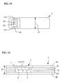
- FIGS. 11 and 12th illustrated embodiment of the proposed concept is reduced the portable data carrier 1 on a contact tongue 12 and has only one USB interface. In this way it functions e.g. as a security token for verification an authorization by means of one stored on the token Software key.
- the external dimensions of the portable shown in FIGS. 11, 12 Data carrier 1 no longer meet the ISO 7810 chip card standard, but instead are matched to a USB socket 16.
- the Card body 2 one on the level 17 of under the contact springs 20A - 20D a USB socket 16 lying space adapted, not standard Thickness 17 '.
- the increased thickness can be easily produced realize by the card body 2 in the usual way like a chip card several layers 2A - 2E, but a correspondingly thicker one Inner layer or additional inner layers 2B - 2D in the Card body structure are introduced.
- the contact arrangement 10 has, as in 11 illustrates exactly four interface contacts CA - CD, the Position on the position of the contact springs 20A - 20D of a USB socket 16 is aligned so that after inserting the data carrier 1 into a USB socket come to lie exactly under these.
- the contact arrangement 10 is expediently located, as in FIG. 12 indicated on the top of a module 3, on the underside of the integrated circuit 4 is arranged.
- the module 3 is preferably after Type of chip card module, i.e. based on a substrate 7, the one can be a suitable film, produced and embedded in the card body 2, typically into a recess 8 prepared therein. Only the shape the contact arrangement 10 is modified as a USB interface.
- integrated circuits 4 is in the Module 3 also expediently an additional integrated circuit 5 arranged, the function of which is to the integrated circuit 4th
- To provide auxiliary functions, in particular a clock signal, which for Operation of a chip card circuit on a USB interface required are.
Abstract
Description
Die Erfindung betrifft tragbare Datenträger, insbesondere in Gestalt von Chipkarten oder Token, und die darauf vorgesehenen Schnittstellen zum Datenaustausch. Noch spezieller befaßt sich die Erfindung mit der physischen Ausgestaltung solcher Schnittstellen.The invention relates to portable data carriers, in particular in the form of Chip cards or tokens, and the interfaces to the Data exchange. The invention is even more particularly concerned with the physical Design of such interfaces.
Chipkarten, die auch als Smart Cards oder Memory Cards bezeichnet werden,
sind in vielfältigen Ausgestaltungen bekannt. Generell weisen Chipkarten einen
dünnen Kartenkörper auf, in dem sich mindestens ein Halbleiterchip befindet.
Hinsichtlich ihrer Abmessungen entsprechen Chipkarten üblicherweise den
Vorgaben der Norm ISO 7810. Die hier insbesondere betrachteten kontaktgebundenen
Chipkarten sind ferner in der Regel gemäß der Norm ISO/IEC
7816 ausgestaltet. Teil 1 dieser Norm definiert die physischen Eigenschaften der
Chipkarte; Teil 2 gibt die Anordnung und Ausgestaltung der Kontaktanordnung
auf der Chipkarte an, und Teil 3 definiert elektrische Eigenschaften und
Übertragungsprotokolle. Die genannte Normen sind über die International
Organization for Standardization, Genf, http:llwww.iso.ch, erhältlich.Chip cards, which are also referred to as smart cards or memory cards , are known in a variety of configurations. In general, chip cards have a thin card body in which there is at least one semiconductor chip. With regard to their dimensions, chip cards usually meet the requirements of the ISO 7810 standard. The contact-based chip cards in particular considered here are also generally designed in accordance with the ISO / IEC 7816 standard.
Zum Datenaustausch mit Chipkarten sind besondere Schnittstellenvorrichtungen erforderlich, die ― abhängig davon, ob sie Bedienungs- und Anzeigeelemente aufweisen oder nicht - üblicherweise als "Terminals" oder "Kartenleser" bezeichnet werden. Die Verwendung solcher Schnittstellenvorrichtungen verursacht jedoch zusätzliche Kosten. Außerdem kann die Chipkarte nur an Geräte angeschlossen werden, die eine geeignete Schnittstellenvorrichtung aufweisen. Dies beschränkt den gegenwärtig üblichen Einsatz von Chipkarten auf einige klar umrissene Anwendungsgebiete.There are special interface devices for data exchange with chip cards required - depending on whether they have controls and indicators or not - usually as "terminals" or "card readers" be designated. The use of such interface devices however causes additional costs. In addition, the chip card can only be used Devices are connected that have a suitable interface device exhibit. This limits the current use of chip cards on some clearly defined areas of application.
Aus den internationalen Patentveröffentlichungen WO 00/16255 A1 und WO 01/69881 A2 sind Chipkarten bekannt, die zwei Schnittstellen aufweisen, nämlich eine erste Schnittstelle gemäß der Norm ISO/IEC 7816 und eine zweite Schnittstelle gemäß der USB-Norm. Unter der Bezeichnung "USB" wird im vorliegenden Dokument der Universal Serial Bus (Universeller Serieller Bus) verstanden, wie er in dem Dokument "Universal Serial Bus Specification" des USB Implementors Forum, Inc., Revision 2.0, 27. April 2000, verfügbar unter http://www.usb.orgldevelopersldocs.html, beschrieben ist.Chip cards are known from the international patent publications WO 00/16255 A1 and WO 01/69881 A2 which have two interfaces, namely a first interface according to the ISO / IEC 7816 standard and a second interface according to the USB standard. In the present document, the term “USB” is understood to mean the universal serial bus as available in the document “ Universal Serial Bus Specification ” of the USB Implementors Forum, Inc., Revision 2.0, April 27, 2000 http: // www.usb.orgldevelopersldocs.html .
Die in den Dokumenten WO 00/16255 A1 und WO 01/69881 A2 beschriebenen Chipkarten sind jedoch lediglich in ihren elektrischen Eigenschaften und hinsichtlich der verwendeten Protokolle mit dem Universal Serial Bus kompatibel. Zur Übertragung der USB-Datensignale werden die bislang noch freien Kontaktflächen C4 und C8 der Kontaktanordnung gemäß ISO/IEC 7816 verwendet. Es ist daher ein spezieller Adapter erforderlich, in den die Chipkarte eingesteckt wird und der die genannten Kontaktflächen mit einem USB-Stecker verbindet. Wenngleich ein solcher Adapter weniger aufwendig als ein üblicher Kartenleser ist, so verursacht er dennoch zusätzliche Kosten. Ferner muß der Adapter ständig mitgeführt werden. Dadurch leidet die Benutzerfreundlichkeit, weil der Adapter erstens größer als die Chipkarte ist und weil er zweitens möglicherweise gerade dann nicht greifbar ist, wenn er dringend benötigt wird.However, the chip cards described in documents WO 00/16255 A1 and WO 01/69881 A2 are only compatible with the universal serial bus in terms of their electrical properties and with regard to the protocols used. The previously free contact areas C4 and C8 of the contact arrangement according to ISO / IEC 7816 are used to transmit the USB data signals. A special adapter is therefore required, into which the chip card is inserted and which connects the mentioned contact areas with a USB connector. Although such an adapter is less expensive than a conventional card reader, it still incurs additional costs. Furthermore, the adapter must always be carried. As a result, user friendliness suffers because, firstly, the adapter is larger than the chip card and, secondly, it may not be available when it is urgently needed.
Die Erfindung hat daher die Aufgabe, die genannten Probleme ganz oder zum Teil zu lösen und einen tragbaren Datenträger insbesondere in Gestalt einer Chipkarte bereitzustellen, der besonders einfach an externe Geräte anschließbar ist. Insbesondere soll zum Anschluß der Chipkarte an einen Computer oder an ein anderes externes Gerät weder eine Schnittstellenvorrichtung noch ein Adapter erforderlich sein. In bevorzugten Ausgestaltungen soll die Chipkarte unmittelbar - also insbesondere ohne Adapter oder Zwischenstecker ― in eine USB-Buchse eines Computers, eines USB-Hubs oder eines USB-Verlängerungskabels einsteckbar sein. Die vorzuschlagende Chipkarte soll zudem ohne wesentliche Änderungen in Ausführung und Herstellungsverfahren als Token ausführbar sein. The object of the invention is therefore to solve all of the above-mentioned problems Part to solve and a portable disk in particular in the form of a To provide a chip card that is particularly easy to connect to external devices is. In particular, to connect the chip card to a computer or to another external device is neither an interface device nor a Adapter may be required. In preferred configurations, the chip card directly - in particular without an adapter or adapter - into one USB socket on a computer, a USB hub or a USB extension cable be insertable. The chip card to be proposed should also without significant changes in design and manufacturing processes be executable as a token.
Erfindungsgemäß wird diese Aufgabe vollständig oder teilweise gelöst durch einen tragbaren Datenträger in Gestalt einer Chipkarte mit mindestens einer Schnittstelle, die Schnittstellenkontakte nutzt, welche auf einer Kontaktzunge der Chipkarte angeordnet sind. Die abhängigen Ansprüche definieren bevorzugte Ausgestaltungen der Erfindung.According to the invention, this object is completely or partially achieved by a portable data carrier in the form of a chip card with at least one Interface that uses interface contacts, which on a contact tongue the chip card are arranged. Define the dependent claims preferred embodiments of the invention.
Die Erfindung geht von der Grundidee aus, Schnittstellenkontakte zumindest einer Schnittstelle auf einer aus dem tragbaren Datenträger herausgebildeten Kontaktzunge vorzusehen. Ist der tragbare Datenträger eine Chipkarte, können die Maße der Kontaktzunge- weitgehend unabhängig von den für Chipkarten durch die einschlägigen Normen vorgegebenen Abmessungen - so gewählt werden, daß die Kontaktzunge wie ein Stecker unmittelbar in eine externe Buchse, an die die Chipkarte angeschlossen werden soll, paßt. In bevorzugten Ausgestaltungen ist diese externe Buchse eine Flachbuchse, welche die Kontaktzunge zumindest seitlich umschließt. Insbesondere kann die Buchse eine USB-Buchse vom Typ "A" sein. Die Breite einer zum Einstecken in eine solche Buchse ausgelegten Kontaktzunge beträgt ungefähr 12 mm. Dies ist schmaler als die Breiten der drei gebräuchlichen, durch die Norm ISO 7810 definierten Chipkartenformate ID-1, ID-00 und ID-000.The invention is based on the basic idea, at least interface contacts an interface on a formed from the portable data carrier Provide contact tongue. If the portable data carrier is a chip card, you can the dimensions of the contact tongue - largely independent of those for chip cards dimensions specified by the relevant standards - so chosen be that the contact tongue like a plug directly into an external Socket to which the chip card is to be connected fits. In preferred This external socket is a flat socket, which the Contact tongue encloses at least on the side. In particular, the socket a USB socket of type "A". The width of one for insertion into one such socket designed contact tongue is approximately 12 mm. This is narrower than the widths of the three common ones, through the ISO 7810 standard defined chip card formats ID-1, ID-00 and ID-000.
In bevorzugter Ausführung weist die Chipkarte mindestens zwei Schnittstellen auf. Die erste Schnittstelle stellt die "übliche" Chipkartenschnittstelle dar, die kontaktgebunden oder kontaktlos ausgestaltet sein kann. Bevorzugt ist die erste Schnittstelle eine kontaktgebundene Schnittstelle gemäß ISO/IEC 7816 mit einer Kontaktanordnung, die insgesamt sechs oder acht Schnittstellenkontakte aufweist. Es kann auch vorgesehen sein, daß die physische Kontaktanordnung der ersten Schnittstelle der Norm ISO/IEC 7816 zwar nicht genau entspricht, aber mit dieser kompatibel ist. Hierunter ist zu verstehen, daß die Kontaktanordnung gegenüber der Norm zusätzliche oder fehlende Kontaktfelder aufweisen kann, wenn nur die benötigten Kontaktfelder an den erforderlichen Stellen vorhanden sind. Die Kontaktanordnung der ersten Schnittstelle befindet sich in manchen Ausgestaltungen der Erfindung - ebenso wie die Kontakte der zweiten Schnittstelle - auf der Kontaktzunge.In a preferred embodiment, the chip card has at least two interfaces on. The first interface is the "usual" chip card interface, the can be configured contact or contactless. The is preferred first interface with a contact interface according to ISO / IEC 7816 a contact arrangement, the total of six or eight interface contacts having. It can also be provided that the physical contact arrangement the first interface does not exactly correspond to the ISO / IEC 7816 standard, but is compatible with this. This means that the Contact arrangement additional or missing compared to the standard Can have contact fields if only the required contact fields on the necessary positions are available. The contact arrangement of the first Interface is in some embodiments of the invention - as well like the contacts of the second interface - on the contact tongue.
Die erste und die zweite Schnittstelle nutzen vorzugsweise zumindest teilweise unterschiedliche Schnittstellenkontakte. So kann beispielsweise für die zweite Schnittstelle mindestens ein zusätzlicher Schnittstellenkontakt vorgesehen sein, also ein Schnittstellenkontakt, der für die erste Schnittstelle nicht verwendet wird. Dieser mindestens eine zusätzliche Schnittstellenkontakt der zweiten Schnittstelle ist in manchen Ausgestaltungen in die Kontaktanordnung der ersten Schnittstelle integriert oder befindet sich in unmittelbarer Nachbarschaft dieser Kontaktanordnung. In anderen Ausführungsformen sind die Kontaktanordnung der ersten Schnittstelle und der/die zusätzliche/n Schnittstellenkontakt/e dagegen auf der Oberfläche der Chipkarte räumlich voneinander getrennt.The first and the second interface preferably use at least partially different interface contacts. For example, for the second Interface at least one additional interface contact may be provided, an interface contact that is not used for the first interface becomes. This at least one additional interface contact the second In some configurations, the interface is in the contact arrangement of the integrated first interface or is in the immediate vicinity this contact arrangement. In other embodiments, the Contact arrangement of the first interface and the additional one / s In contrast, interface contact (s) spatially on the surface of the chip card separated from each other.
In bevorzugten Ausgestaltungen ist die Kontaktzunge in einem inneren Bereich der Chiparte ausgebildet, der allseitig vom Außenrand der Chipkarte getrennt ist. Beispielsweise kann die Kontaktzunge dadurch gebildet sein, daß die Chipkarte mit einem U-förmigen Schlitz versehen ist. Der von diesem Schlitz umgebene Innenbereich der Chipkarte bildet die Kontaktzunge. In alternativen Ausgestaltungen kann die Kontaktzunge auch am Rand der Chipkarte angeordnet sein. Dies beinhaltet auch Ausführungsformen, bei denen die Kontaktzunge in einem inneren Bereich der Chipkarte beginnt und am Rand des durch die Norm ISO 7810 definierten Kartenformats endet.In preferred configurations, the contact tongue is in an inner area the chip card is formed, which is separated on all sides from the outer edge of the chip card is. For example, the contact tongue can be formed in that the Chip card is provided with a U-shaped slot. The one from this slot Surrounded inner area of the chip card forms the contact tongue. In alternatives The contact tongue can also be configured at the edge of the chip card be arranged. This also includes embodiments in which the Contact tongue begins in an inner area of the chip card and on the edge of the card format defined by the ISO 7810 standard ends.
Insbesondere bei Ausgestaltungen, die eine vom Außenrand der Chipkarte entfernte Kontaktzunge aufweisen, ist die Kontaktzunge vorzugsweise reversibel aus der Chipkartenebene herausbiegbar oder herausklappbar und wieder in die Chipkartenebene zurückbiegbar oder zurückklappbar. Eine biegbare Kontaktzunge kann insbesondere einstückig mit der restlichen Chipkarte aus einem flexiblen Kunststoffmaterial gebildet sein. Bei einer klappbaren Kontaktzunge kann dagegen ein Scharnier und/oder mindestens eine Schnapphalterung, die die Kontaktzunge in ihrer Lage in der Chipkartenebene fixiert, vorgesehen sein.In particular in the case of configurations which extend from the outer edge of the chip card have removed contact tongue, the contact tongue is preferred reversibly bendable or foldable out of the chip card level and can be bent back or folded back into the chip card level. A bendable contact tongue can in particular in one piece with the rest Chip card can be formed from a flexible plastic material. At a foldable contact tongue, however, can be a hinge and / or at least a snap bracket that holds the tab in place Fixed chip card level, be provided.
In weiteren bevorzugten Ausgestaltungen weist die Kontaktzunge seitlich angebrachte, klappbare Stege auf, um z.B. einen USB-Stecker mit einer größeren Dicke als der Chipkartendicke nachzubilden. Die Kontaktzunge bildet vorzugsweise einen dauerhaften Bestandteil der Chipkarte, so daß eine wiederholte und abwechselnde Verwendung der ersten und der zweiten Schnittstelle möglich ist. Dies stellt ein weiteres Unterscheidungsmerkmal der vorliegenden Chipkarte zu den im Mobiltelefonbereich bekannten Chipkarten dar, die auf einer Trägerkarte im Format ID-1 eine irreversibel ausbrechbare, kompakte Chipkarte im Format ID-000 enthalten.In further preferred configurations, the contact tongue faces laterally attached, foldable webs to e.g. a USB plug with a greater thickness than the chip card thickness. The contact tongue forms preferably a permanent part of the chip card, so that a repeated and alternating use of the first and the second Interface is possible. This represents another distinguishing feature of the present chip card to the chip cards known in the field of mobile phones which, on a carrier card in the ID-1 format, is an irreversibly breakable Compact chip card in ID-000 format included.
Ausführungsformen der Chipkarte, bei denen die zweite Schnittstelle eine USB-Schnittstelle ist, sind besonders geeignet zum Anschluß der Chipkarte an gegenwärtig übliche Computer. Bevorzugt sind alle aktiven Schnittstellenkontakte der Chipkarte mit mindestens einem Halbleiterchip verbunden, welcher ― beispielsweise auf die in den Dokumenten WO 00/16255 A1 und WO 01/69881 A2 beschriebene Weise - die elektrischen Signale beider Schnittstellen empfängt, sendet und verarbeitet.Embodiments of the chip card, in which the second interface is a USB interface are particularly suitable for connecting the chip card currently common computers. All active are preferred Interface contacts of the chip card with at least one semiconductor chip connected, which - for example to those in the documents WO 00/16255 A1 and WO 01/69881 A2 described way - the electrical Receives, sends and processes signals from both interfaces.
Ein bevorzugtes Anwendungsgebiet der Erfindung sind sogenannte Internet-Chipkarten, die einen kompakten Internet-Server implementieren. Ein auf einem externen Computer laufender Internet-Browser kommuniziert über die zweite Schnittstelle - z.B. die USB-Schnittstelle ― mit dem Server und stellt eine Benutzeroberfläche zur Interaktion mit der Chipkarte bereit. Die Erfindung ist jedoch auch für viele weitere Anwendungsgebiete nützlich, so z.B. immer dann, wenn umfangreiche Daten zwischen einer Chipkarte und einem externen Gerät übertragen werden sollen. A preferred field of application of the invention is so-called internet chip cards, who implement a compact internet server. One on an external computer running Internet browser communicates via the second interface - e.g. the USB interface - with the server and provides one User interface ready for interaction with the chip card. The invention is but also useful for many other areas of application, e.g. always then, if there is extensive data between a chip card and an external device should be transferred.
In einer weiteren vorteilhaften Umsetzung des Erfindungsgedankens sind die Außenabmessungen des tragbaren Datenträgers und die Lage der Schnittstelle darauf so gewählt, daß der Datenträger an der Schnittstellenseite einen voll zu einer USB-Buchse kompatiblen Stecker bildet. Vorzugsweise ist bei dieser Ausführung auch die Dicke des Kartenkörpers an die Verhältnisse in einer USB-Buchse angepaßt. Derartig ausgebildete tragbare Datenträger eignen sich insbesondere als in Hardware ausgeführte Softwareschlüssel oder "Token", mit denen z.B die Berechtigung eines Nutzers zur Nutzung eines Gerätes nachgewiesen wird. Solche Token lassen sich vorteilhaft mittels gängiger Herstellungsmethoden fertigen, wie sie in der Chipkartenfertigung eingesetzt werden.In a further advantageous implementation of the inventive concept, the External dimensions of the portable data carrier and the location of the interface then chosen so that the data carrier on the interface side is fully closed a compatible USB connector. Preferably this one Execution also the thickness of the card body to the conditions in a USB socket customized. Portable data carriers designed in this way are suitable in particular as software keys or "tokens" executed in hardware e.g. the authorization of a user to use a device is proven. Such tokens can be advantageously used by means of common ones Manufacture manufacturing methods as used in chip card production become.
Weitere Merkmale, Aufgaben und Vorteile der Erfindung ergeben sich aus der
folgenden Beschreibung mehrerer Ausführungsbeispiele und
Ausführungsalternativen der Erfindung. Es wird auf die schematischen
Zeichnungen verwiesen, in denen zeigen:
Fig. 1 zeigt einen tragbaren Datenträger 1 in Gestalt einer Chipkarte mit einem
Kartenkörper 2, in den ein Modul 3 eingebettet ist, worin sich ein Halbleiterchip
mit einem integrierten Schaltkreis 4 befindet, und einer Kontaktanordnung 10.
Die Chipkarte entspricht in ihren Außenabmessungen dem Format ID-1 gemäß
der Norm ISO 7810. Die Chipkarte weist eine erste und eine zweite Schnittstelle
zur Kommunikation mit externen Geräten auf. Hierbei ist die erste Schnittstelle
eine "übliche" Chipkartenschnittstelle, die in ihren physischen und elektrischen
Eigenschaften und hinsichtlich der eingesetzten Protokolle der Norm
ISO/IEC 7816 entspricht. Die zweite Schnittstelle ist im vorliegenden
Ausführungsbeispiel eine USB-Schnittstelle, mittels derer die Chipkarte unmittelbar
an einen Computer oder ein sonstiges mit einer USB-"A"-Buchse
ausgestattetes Gerät angeschlossen werden kann.Fig. 1 shows a
An der durch Teil 2 der Norm ISO/IEC 7816 definierten Position weist die
Chipkarte eine Kontaktanordnung 10 auf, die in Fig. 4 genauer dargestellt ist.
Die Kontaktanordnung 10 enthält an den ebenfalls durch Teil 2 der Norm
ISO/IEC 7816 definierten Stellen insgesamt acht Schnittstellenkontakte C 1, C2,
C3, C4, C5, C6, C7, C8 der ersten Schnittstelle. Ferner sind in die Kontaktanordnung
10 gemäß Fig. 1 und Fig. 4 insgesamt vier weitere Schnittstellenkontakte
CA, CB, CC, CD integriert, die der zweiten Schnittstelle zugeordnet
sind. Im vorliegenden Ausführungsbeispiel sind sämtliche Schnittstellenkontakte
C1 - C8 und CA - CD als mit der Chipkarten-Oberfläche ungefähr bündige
Kontaktflächen ausgestaltet, während in Abwandlungen insbesondere für die
zusätzlichen Schnittstellenkontakte CA - CD andere Ausgestaltungen
vorgesehen sein können.At the position defined by
Die Kontaktanordnung 10 befindet sich auf einer Kontaktzunge 12, die im vorliegenden
Ausführungsbeispiel dadurch gebildet ist, daß ein dreiseitig
umlaufender, U-förmiger Schlitz in das Trägermaterial der Chipkarte eingearbeitet
ist. An dem in Fig. 1 rechts gezeigten Ansatzpunkt der Kontaktzunge
12 geht die Kontaktzunge 12 integral in die restliche Chipkarte über. Die Dicke
13 der Kontaktzunge 12 entspricht der normgemäßen Dicke der Chipkarte. An
der in Fig. 1 links gezeigten Spitze der Kontaktzunge befindet sich die
Kontaktanordnung 10. Die Breite der Kontaktzunge 12 beträgt im vorliegenden
Ausführungsbeispiel ungefähr 12 mm, während die Kontaktanordnung 10 -
gemäß Teil 2 der Norm ISO/IEC 7816 - vom oberen Rand des Kontaktfeldes CA
zum unteren Rand des Kontaktfeldes CD eine Mindestgröße von ungefähr
9,3 mm aufweist.The
Als Material für den Kartenkörper wird im vorliegenden Ausführungsbeispiel ein
flexibles Kunststoffmaterial, beispielsweise PVC, ABS oder PET, verwendet. In
das Trägermaterial der Chipkarte ist in an sich bekannter Weise ein
Halbleiterchip eingearbeitet, der in Fig. 1 von dem Kontaktfeld 10 verdeckt ist.
Der Kartenkörper kann in Ausführungsalternativen auch besonders hochwertige
Materialien wie Folienverbundwerkstoffe oder Metalle aufweisen, um eine hohe
Lebensdauer zu gewährleisten. Dies gilt insbesondere für die unten noch
genauer zu beschreibenden Ausführungsvarianten gemäß Fig. 6 - Fig. 10.In the present exemplary embodiment, a is used as the material for the card body
flexible plastic material, such as PVC, ABS or PET, used. In
the carrier material of the chip card is in a manner known per se
Semiconductor chip incorporated, which is covered by the
Bei der Ausgestaltung gemäß Fig. 1 besteht die Kontaktzunge 12 aus demselben
flexiblen Material wie der restliche Kartenkörper. Daher kann die Kontaktzunge
12 ohne Beschädigung aus der durch die Chipkarte definierten Ebene
herausgebogen werden, wie dies in Fig. 2 gezeigt ist. Die Kontaktzunge 12
paßt wegen ihrer Breite von ungefähr 12 mm genau in eine an sich bekannte
USB-Buchse 16 vom Typ "A". In der Darstellung von Fig. 2 ist die zum Betrachter
weisende Seitenwand der USB-Buchse 16 teilweise weggebrochen
gezeichnet, so daß ein Kontakthalter 18 und eine Kontaktfeder 20 sichtbar
sind. Wie aus Fig. 2 in Verbindung mit Fig. 4 hervorgeht, ist der Abstand der zur
USB-Schnittstelle gehörenden Schnittstellenkontakte CA - CD von der Spitze
der Kontaktzunge 12 so gewählt, daß die Kontaktfeder 20 der USB-Buchse 16
bei maximal eingesteckter Kontaktzunge 12 eine elektrische Verbindung mit
einem dieser Schnittstellenkontakte CA - CD herstellt.1, the
Aus dem in Fig. 3 dargestellten Querschnitt ist ersichtlich, daß im eingesteckten
Zustand der Kontaktzunge 12 je eine von vier Kontaktfedern 20A, 20B, 20C,
20D der USB-Buchse 16 je einen der vier zur USB-Schnittstelle gehörenden
Schnittstellenkontakte CA - CD kontaktiert. Dies trifft im vorliegenden
Ausführungsbeispiel trotz der Tatsache zu, daß die Ausgestaltung der Schnittstellenkontakte
CA - CD als Kontaktfelder und ihre Dimensionierung an die
Norm ISO/IEC 7816 - und nicht primär an die USB-Norm - angelehnt ist. Die
Kontaktfedern 20A - 20D liegen daher, wie in Fig. 3 dargestellt, nicht genau
mittig auf den Kontaktflächen der Schnittstellenkontakte CA - CD auf; dies ist
jedoch unschädlich. In Ausführungsalternativen ist dagegen vorgesehen, die
Schnittstellenkontakte CA - CD weitgehend gemäß den Vorgaben der USB-Norm
auszugestalten.From the cross section shown in Fig. 3 it can be seen that in the inserted
State of the
Im Betrieb kann die Chipkarte in ihrer flachen, in Fig. 1 gezeigten Konfiguration
wie eine übliche ISO/IEC-7816-Chipkarte verwendet und beispielsweise in ein
Kartenterminal oder einen Kartenleser eingeführt werden. Der in der Chipkarte
befindliche Halbleiterchip erkennt diese erste Betriebsweise und stellt elektrisch
und logisch eine ISO/IEC-7816-kompatible Schnittstelle zur Verfügung, deren
Signale über die acht Schnittstellenkontakte C1 - C8 der Kontaktanordnung 10
geführt werden.In operation, the smart card can be in its flat configuration, shown in FIG
used as a standard ISO / IEC-7816 chip card and for example in one
Card terminal or a card reader are introduced. The one in the chip card
located semiconductor chip recognizes this first mode of operation and provides electrical
and logically an ISO / IEC-7816-compatible interface is available, whose
Signals via the eight interface contacts C1 - C8 of the
Ferner kann die Chipkarte, wie in Fig. 2 gezeigt, unmittelbar in die USB-Buchse
16 beispielsweise eines Computers oder eines anderen Geräts eingesteckt
werden. Der Halbleiterchip der Chipkarte paßt sich auch diesem zweiten Betriebsmodus
an, indem er eine elektrisch und logisch USB-kompatible Schnittstelle
bereitstellt, deren Signale über die vier zusätzlichen Schnittstellenkontakte
CA - CD laufen. Wird die Chipkarte aus der USB-Buchse 16 herausgezogen, so
biegt sich die Kontaktzunge 12 durch die Elastizität des für die Chipkarte
verwendeten Trägermaterials in die Chipkartenebene zurück, so daß wieder die
flache Konfiguration gemäß Fig. 1 erreicht ist.Furthermore, as shown in FIG. 2, the chip card can be inserted directly into the
Fig. 5 zeigt eine gegenüber Fig. 4 abgewandelte Anordnung der Schnittstellenkontakte
C1 - C8 und CA - CD. Die zusätzlichen Schnittstellenkontakte CA -
CD der zweiten Schnittstelle - vorliegend der USB-Schnittstelle - sind hierbei
nicht in die ISO/IEC-7816-kompatible Kontaktanordnung 10 integriert. Vielmehr
befinden sich die zusätzlichen Schnittstellenkontakte CA - CD unmittelbar
neben einer Kontaktanordnung 10', die exakt der Norm ISO/IEC 7816
entspricht und die nur die acht gemäß dieser Norm vorgesehenen
Schnittstellenkontakte C1 - C8 aufweist. Die Ausgestaltung nach Fig. 5
ermöglicht es, die Schnittstellenkontakte CA - CD besonders nahe an der Spitze
der Kontaktzunge 12 anzuordnen. Überdies wird vermieden, daß die
Kontaktfedern 20A - 20D beim Einstecken der Kontaktzunge 12 in die
USB-Buchse 16 kurzzeitig über die Schnittstellenkontakte C1 - C4 streifen.FIG. 5 shows an arrangement of the interface contacts modified compared to FIG. 4
C1 - C8 and CA - CD. The additional interface contacts CA -
CD of the second interface - here the USB interface - are here
not integrated in the ISO / IEC-7816-
In der Auführungsvariante gemäß Fig. 6 befinden sich seitlich an der Spitze der
Kontaktzunge 12 ― über und unter der Kontaktanordnung 10 ― zwei klappbare
Stege 22A, 22B. Diese Stege 22A, 22B gleichen den Höhenunterschied
zwischen der Normdicke 13 einer Chipkarte und der definierten Höhe 17 der
Einschuböffnung, d.h. des unter den Kontaktfedern 20 A - 20 D befindlichen
Steckraumes, einer USB-Buchse 16 aus und sind entsprechend dimensioniert.
Die Stege 22A, 22B können vor dem Einstecken der Kontaktzunge 12 in die
USB-Buchse 16 im rechten Winkel umgeklappt werden, und verbessern den
Halt der Kontaktzunge 12 in der USB-Buchse 16, indem sie die vertikale
Bewegungsfreiheit der Kontaktzunge 12 in der USB-Buchse 16 reduzieren. 6 are located laterally at the top of the
Contact tongue 12 - above and below the contact arrangement 10 - two
Auch die Stege 22A, 22B können nach Gebrauch wieder in eine flache
Konfiguration zurückgeklappt werden, wobei sie von entsprechend
verbreiterten Bereichen des Schlitzes 14 aufgenommen werden.The
Fig. 6 A veranschaulicht eine Ausführungsvariante, bei der der Höhenausgleich
von der Dicke 13 der Kontaktzunge 12 zu der Höhe 17 einer USB-Buchse 16
mit Hilfe einer zusätzlichen Füllkarte F erreicht wird. Die Füllkarte F entspricht in
ihren Abmessungen einer Chipkarte und besitzt an derselben Position wie die
Chipkarte eine biegsame Zunge 12A. Ihre Dicke ist so bemessen, daß die bei
Übereinanderlegen von Füllkarte und Chipkarte resultierende Gesamtdicke
genau der Höhe einer USB-Buchse 16 entspricht. An der Oberseite der Füllkarte
F sind Verbindungsmittel ausgebildet, um die Füllkarte lösbar an einer Chipkarte
befestigen zu können. Die Verbindung erfolgt dabei so, daß Füllkarte und
Chipkarte, damit Kontaktzunge 12 und Zunge 12 A, genau übereinander
liegen. Als Verbindungsmittel kommt beispielsweise eine mehrfach nutzbare
Haftklebeschicht in Betracht. Weiter können die Verbindungsmittel eine
Formgebung umfassen, welche die Verbindung unterstützt. Beispielsweise
können auf der Füllkarte kleine Aufwölbungen angelegt sein, die in
korrespondierende Mulden auf der Chipkarte greifen.6 A illustrates an embodiment variant in which the height compensation
from the
Zur Nutzung wird die, grundsätzlich separat gehandhabte Füllkarte F an der
Chipkarte befestigt. Anschließend werden die danach übereinanderliegenden
Zungen 12, 12A gemeinsam aus der Kartenebene herausgebogen und
gemeinsam in die USB-Buchse 16 gesteckt. Aufgrund der aufeinander
abgestimmten Dimensionen sitzt das Zungenpaar 12, 12A fest in der USB-Buchse.The filler card F, which is generally handled separately, is used
Chip card attached. Then the ones lying on top of each
Da ein häufiges Biegen der Kontaktzunge 12 möglicherweise der Lebensdauer
der Chipkarte abträglich sein könnte, ist in der Ausführungsalternative gemäß
Fig. 7 ein Scharnier 24 zur klappbaren Verbindung der Kontaktzunge 12 mit der
restlichen Chipkarte vorgesehen. Die Kontaktzunge 12 - oder sogar die
gesamte Chipkarte - kann dann aus einem relativ starren Material,
beispielsweise auch Metall, gefertigt sein. Das Scharnier 24 kann so ausgestaltet
sein, daß die Kontaktzunge 12 mit einer gewissen Rückstellkraft in die flache
Konfiguration der Chipkarte gedrängt wird. Alternativ oder zusätzlich können
auch Schnapphalterungen 26A, 26B, 26C im umlaufenden Schlitz 14
vorgesehen sein, mit denen sich die Kontaktzunge 12 nach dem Rückklappen in
der ursprünglichen Lage fixieren läßt.Because frequent flexing of the
Bei den bisher beschriebenen Ausgestaltungen war die Kontaktzunge 12 in
einem inneren Bereich der Chipkarte, also mit allseitigem Abstand vom äußeren
Rand der Chipkarte, angeordnet. In Fig. 8, Fig. 9 und Fig. 10 sind dagegen
Ausführungsbeispiele gezeigt, bei denen die Kontaktzunge 12 am Rand der
Chipkarte angeordnet ist. Die Kontakte C1 - C8 der ersten Schnittstelle in der
Kontaktanordnung 10' sind hierbei räumlich von den Kontakten CA - CD der
zweiten Schnittstelle entfernt. Dies hat den Vorteil, daß hinsichtlich der
Ausgestaltung der Schnittstellenkontakte C1 - C8 und CA - CD weniger
gegenseitige Abhängigkeiten und Einschränkungen bestehen. So können beispielsweise
die Schnittstellenkontakte CA - CD in Fig. 8 bis Fig. 10 hinsichtlich
ihrer Geometrie weitgehend oder vollständig gemäß der USB-Norm ausgestaltet
sein.In the configurations described so far, the
Bei dem Ausführungsbeispiel gemäß Fig. 8 ist die Kontaktzunge 12 durch zwei
Einschnitte 28A, 28B von der restlichen Chipkarte getrennt. Die Kontaktzunge
12 kann flexibel ausgestaltet sein, um das Einstecken in eine fest eingebaute
USB-Buchse 16 zu erleichtern. Bei einer starren Kontaktzunge 12 wird sich die
Chipkarte gemäß Fig. 8 in der Regel nur in eine USB-Buchse 16 eines USB-Verlängerungskabels
einstecken lassen, deren Seitenrand in die Einschnitte 28A,
28B paßt.8, the
Die Einschnitte 28A, 28B können in weiteren Ausführungsformen auch breiter
ausgestaltet sein, im Extremfall so breit, daß die Kartenbereiche oberhalb und
unterhalb der Kontaktzunge 12 ganz wegfallen. Eine derartige Ausgestaltung
ist in Fig. 9 dargestellt. Die dort gezeigte Chipkarte läßt sich in nahezu jede -
auch in eine in einen Computer fest eingebaute ― USB-Buchse 16 einstecken.
Allerdings entspricht die Chipkarte hinsichtlich ihrer Außenabmessungen nicht
mehr der Norm ISO 7810, was bei einer Verwendung in Kartenlesern oder
Kartenterminals möglicherweise zu Schwierigkeiten führen könnte. Um solche
Probleme zu vermeiden, sind bei der Ausgestaltung gemäß Fig. 10 die durch die
Norm ISO 7810 vorgegebenen Außenmaße möglichst weitgehend eingehalten.The
Es versteht sich, daß die oben beschriebenen und in den Figuren gezeigten Merkmale in weiteren Ausführungsalternativen auf vielfältige Weise miteinander kombiniert werden können. So können z.B. auch die Ausgestaltungen nach Fig. 8 - Fig. 10 mit Scharnieren oder klappbaren Stegen oder Schnapphalterungen - wie in Fig. 6 und Fig. 7 gezeigt ― versehen werden. Ferner ist eine räumliche Trennung der Schnittstellenkontakte der,ersten und der zweiten Schnittstelle wie in Fig. 8 - Fig. 10 auch bei einer in einem inneren Bereich der Chipkarte angeordneten Kontaktzunge 12 - wie in Fig. 1 gezeigt - möglich.It is understood that those described above and shown in the figures Features in further alternative designs in a variety of ways can be combined. For example, also the designs 8-10 with hinges or foldable webs or snap holders - As shown in Fig. 6 and Fig. 7 - provided. Furthermore is a spatial separation of the interface contacts of the first and second Interface as in FIGS. 8-10 also in the case of an inner region of the Chip card arranged contact tongue 12 - as shown in Fig. 1 - possible.
Die vorstehend beschriebenen Ausgestaltungen beruhen alle auf dem Ansatz,
daß der tragbare Datenträger 1 zumindest die Funktionalität einer Chipkarte
besitzt und entsprechend zwei Schnittstellen, nämlich eine ISO- und eine USB-Schnittstelle
aufweist. In einer vorteilhaften, in den Fig. 11 und 12
veranschaulichten Ausgestaltung des vorgeschlagenen Konzeptes reduziert sich
der tragbare Datenträger 1 auf eine Kontaktzunge 12 und besitzt nur noch eine
USB-Schnittstelle. Dergestalt fungiert er z.B. als Sicherheitstoken zum Nachweis
einer Berechtigung mittels eines auf dem Token gespeicherten
Softwareschlüssels.The configurations described above are all based on the approach
that the
Die Außenabmessungen des in den Fig. 11, 12 gezeigten tragbaren
Datenträgers 1 genügen nicht mehr der Chipkarten-Norm ISO 7810, sondern
sind auf eine USB- Buchse 16 abgestimmt. Die vordere Breite 21' entspricht
daher paßgenau der Breite 21 einer USB-Buchse 16. Weiter besitzt der
Kartenkörper 2 eine auf die Höhe 17 des unter den Kontaktfedern 20A - 20D
einer USB-Buchse 16 liegenden Steckraumes angepaßte, nicht normgerechte
Dicke 17'. Die erhöhte Dicke läßt sich bei Herstellung in einfacher Weise
realisieren, indem der Kartenkörper 2 in üblicher Weise wie eine Chipkarte aus
mehreren Schichten 2A - 2E aufgebaut, dabei aber eine entsprechend dickere
Innenschicht oder zusätzliche Innenschichten 2B - 2D in den
Kartenkörperaufbau eingebracht werden.The external dimensions of the portable shown in FIGS. 11, 12
Abgestimmt auf eine USB-Buchse 16 besitzt die Kontaktanordnung 10, wie in
Fig. 11 veranschaulicht, genau vier Schnittstellenkontakte CA - CD, deren
Position auf die Lage der Kontaktfederen 20A - 20D einer USB-Buchse 16
ausgerichtet ist, so daß sie nach Einstecken des Datenträgers 1 in eine USB-Buchse
genau unter diesen zu liegen kommen.Matched to a
Zweckmäßig befindet sich die Kontaktanordnung 10, wie in Fig. 12
angedeutet, auf der Oberseite eines Modules 3, an dessen Unterseite der
integrierte Schaltkreis 4 angeordnet ist. Das Modul 3 wird vorzugsweise nach
Art eines Chipkartenmodules, d.h. basierend auf einem Substrat 7, das eine
geeignete Folie sein kann, hergestellt und in den Kartenkörper 2 eingebettet,
typischerweise in eine darin vorbereitete Ausnehmung 8. Lediglich die Gestalt
der Kontaktanordnung 10 wird als USB-Schnittstelle abgewandelt. Um für
Chipkarten übliche integrierte Schaltkreise 4 einsetzen zu können, wird in dem
Modul 3 zweckmäßig ferner ein zusätzlicher integrierter Schaltkreis 5
angeordnet, dessen Funktion darin besteht, dem integrierten Schaltkreis 4
Hilfsfunktionen zur Verfügung zu stellen, insbesondere ein Taktsignal, die zum
Betrieb eines Chipkartenschaltkreises an einer USB-Schnittstelle erforderlich
sind.The
Claims (22)
Priority Applications (1)
| Application Number | Priority Date | Filing Date | Title |
|---|---|---|---|
| EP06008084A EP1724713A3 (en) | 2002-12-12 | 2003-12-08 | Portable data carrier |
Applications Claiming Priority (4)
| Application Number | Priority Date | Filing Date | Title |
|---|---|---|---|
| DE10258158 | 2002-12-12 | ||
| DE10258158 | 2002-12-12 | ||
| DE10344049 | 2003-09-23 | ||
| DE10344049A DE10344049A1 (en) | 2002-12-12 | 2003-09-23 | Portable disk |
Related Child Applications (1)
| Application Number | Title | Priority Date | Filing Date |
|---|---|---|---|
| EP06008084A Division EP1724713A3 (en) | 2002-12-12 | 2003-12-08 | Portable data carrier |
Publications (3)
| Publication Number | Publication Date |
|---|---|
| EP1429283A2 true EP1429283A2 (en) | 2004-06-16 |
| EP1429283A3 EP1429283A3 (en) | 2004-07-14 |
| EP1429283B1 EP1429283B1 (en) | 2007-11-07 |
Family
ID=32327516
Family Applications (2)
| Application Number | Title | Priority Date | Filing Date |
|---|---|---|---|
| EP03028151A Expired - Lifetime EP1429283B1 (en) | 2002-12-12 | 2003-12-08 | Portable data carrier |
| EP06008084A Withdrawn EP1724713A3 (en) | 2002-12-12 | 2003-12-08 | Portable data carrier |
Family Applications After (1)
| Application Number | Title | Priority Date | Filing Date |
|---|---|---|---|
| EP06008084A Withdrawn EP1724713A3 (en) | 2002-12-12 | 2003-12-08 | Portable data carrier |
Country Status (4)
| Country | Link |
|---|---|
| EP (2) | EP1429283B1 (en) |
| AT (1) | ATE377808T1 (en) |
| DE (2) | DE10344049A1 (en) |
| ES (1) | ES2294237T3 (en) |
Cited By (21)
| Publication number | Priority date | Publication date | Assignee | Title |
|---|---|---|---|---|
| WO2005031639A1 (en) * | 2003-09-23 | 2005-04-07 | Giesecke & Devrient Gmbh | Portable data support |
| WO2005086086A1 (en) * | 2004-02-27 | 2005-09-15 | Imation Corp. | Credit card sized memory card with host connector |
| WO2006018230A1 (en) | 2004-08-12 | 2006-02-23 | Giesecke & Devrient Gmbh | Method for the production of a portable data support |
| WO2006027027A1 (en) * | 2004-09-07 | 2006-03-16 | Freecom Technologies B.V. | Chip card with usb connector |
| GB2427047A (en) * | 2005-06-08 | 2006-12-13 | Max Wehebrink | Smartcard having a USB plug |
| WO2007091914A1 (en) | 2006-02-09 | 2007-08-16 | Balchaitis Vadim Evgenevich | Plastic card provided with electric contacts |
| EP1843277A1 (en) * | 2006-04-04 | 2007-10-10 | Axalto SA | USB chip card |
| US7344072B2 (en) | 2006-04-27 | 2008-03-18 | Sandisk Corporation | Credit card sized USB flash drive |
| WO2008007139A3 (en) * | 2006-07-10 | 2008-03-27 | Hes Ltd | Memory devices and security systems and apparatus for use with such memory devices |
| GB2450864A (en) * | 2007-06-16 | 2009-01-14 | Martin Edminson | USB Business card |
| EP2069944A2 (en) * | 2006-09-22 | 2009-06-17 | Wenngren Inc. | Method of using a foldable card as a usb contact |
| DE102008019571A1 (en) * | 2008-04-18 | 2009-10-22 | Giesecke & Devrient Gmbh | Chip card and method for its production |
| EP2264648A1 (en) | 2006-05-09 | 2010-12-22 | Zina Lindemann | Data storage card having multiple interfaces |
| WO2011011657A1 (en) * | 2009-07-24 | 2011-01-27 | Echostar Technologies Llc | Expanded smart card interface |
| US8061623B2 (en) | 2006-02-09 | 2011-11-22 | Vadim Evgenevich Balchaytis | Plastic card provided with electrical contacts |
| WO2012069823A1 (en) * | 2010-11-22 | 2012-05-31 | Goosewire Ip Limited | Adapter and card |
| DE102010054061A1 (en) | 2010-12-10 | 2012-06-14 | Giesecke & Devrient Gmbh | Portable system for authenticating person e.g. during opening of account in bank, has integrated semiconductor chip comprising evaluation unit for evaluating user input and storage region for storing user input |
| EP2511854A1 (en) * | 2011-04-15 | 2012-10-17 | Walton Advanced Engineering Inc. | Thin data storage device |
| DE102011121342A1 (en) * | 2011-12-16 | 2013-06-20 | Giesecke & Devrient Gmbh | Card-shaped data carrier such as chip card or smart card, comprises a rotary element which is rotatably supported manually about an axis which is formed parallel to the main surface of the data carrier plane |
| FR2986093A1 (en) * | 2012-01-23 | 2013-07-26 | Emmanuel Thibaudeau | Interactive terminal for capturing image in universal serial bus key in Eiffel tower, has programming unit utilized for programming chip, where chip is programmed with address indicating where captured images are stored on remote server |
| EP2693372A3 (en) * | 2012-07-31 | 2015-10-14 | Walton Advanced Engineering Inc. | A composite card-type structure |
Families Citing this family (11)
| Publication number | Priority date | Publication date | Assignee | Title |
|---|---|---|---|---|
| DE102005049256A1 (en) * | 2005-10-14 | 2007-04-26 | Infineon Technologies Ag | Chip card module has card contacts with contact surface and chip on opposite side from contact surface with integrated circuit and contacts at least partly connected to card contacts |
| FR2896321B1 (en) * | 2006-01-16 | 2008-05-02 | Emmanuel Thibaudeau | COMPUTER ACCESSORY AND APPLICATION |
| FR2910151A1 (en) * | 2006-12-14 | 2008-06-20 | Sagem Defense Securite | Rectangular shaped electronic chip device manufacturing method for electronic chip reading system, involves inserting micro module in thickness of part so that introduction of part establishes electrical connections between contacts |
| WO2008087317A2 (en) * | 2006-12-14 | 2008-07-24 | Sagem Securite | Peripheral security device |
| FR2944368B1 (en) * | 2009-04-09 | 2012-03-02 | Oberthur Technologies | MEMORY KEY ASSEMBLY COMPRISING A MICROCIRCUIT CARD |
| DE102009022787A1 (en) * | 2009-05-27 | 2010-12-02 | Arman Emami | Electronic storage medium, particularly universal serial bus memory stick, has surface made of elastic material, which is provided with recess, where recess limits total area such that subarea is generated |
| FR2973541B1 (en) * | 2011-04-01 | 2014-01-03 | Serge Zareh Alagy | CARD DATA MANAGEMENT SYSTEM AND METHOD RELATING THERETO |
| DE102011112031A1 (en) * | 2011-05-11 | 2012-11-15 | Giesecke & Devrient Gmbh | Method for data exchange between terminal and chip card |
| DE102011103281A1 (en) * | 2011-05-26 | 2012-11-29 | Giesecke & Devrient Gmbh | Portable data carrier i.e. universal subscriber identity module, for use in e.g. mobile phone to identify subscriber in mobile communications network, has contact field surface corresponding to more than specific value of main side surface |
| US9147147B2 (en) | 2014-02-26 | 2015-09-29 | Giesecke & Devrient America, Inc. | Plug-in portable data carrier with semi-detachable token holder |
| DE102015003970A1 (en) | 2015-03-24 | 2016-09-29 | Kingston Technology Company, Inc. | Holder for an electronic data storage |
Citations (8)
| Publication number | Priority date | Publication date | Assignee | Title |
|---|---|---|---|---|
| US3702464A (en) * | 1971-05-04 | 1972-11-07 | Ibm | Information card |
| EP0409241A1 (en) * | 1989-07-19 | 1991-01-23 | Kabushiki Kaisha Toshiba | IC card with additional terminals and method of controlling the IC card |
| DE29819389U1 (en) * | 1998-10-30 | 1999-01-28 | Orga Kartensysteme Gmbh | Smart card |
| DE19737565A1 (en) * | 1997-08-28 | 1999-03-04 | Etr Elektronik Und Technologie | Electronically read chip card |
| WO2000016255A1 (en) * | 1998-09-11 | 2000-03-23 | Schlumberger Systemes | Data transmission method and card therefor |
| WO2000073988A1 (en) * | 1999-05-31 | 2000-12-07 | Gemplus | Portable integrated circuit device and method for the production thereof |
| WO2001096990A2 (en) * | 2000-06-15 | 2001-12-20 | Rainbow Technologies, B.V. | Usb-compliant personal key using a smartcard processor and a smartcard reader emulator |
| WO2003027946A1 (en) * | 2001-09-24 | 2003-04-03 | Gemplus | Dongle which is intended to be connected to a port of a telecommunications device |
Family Cites Families (4)
| Publication number | Priority date | Publication date | Assignee | Title |
|---|---|---|---|---|
| FR2732790B1 (en) * | 1995-04-05 | 1997-05-09 | Gemplus Card Int | INFORMATION COLLECTION SYSTEM FOR CARD READERS |
| DE19624631C2 (en) * | 1996-06-20 | 2002-06-27 | Zentr Mikroelekt Dresden Gmbh | Card arrangement |
| US6343364B1 (en) * | 2000-07-13 | 2002-01-29 | Schlumberger Malco Inc. | Method and device for local clock generation using universal serial bus downstream received signals DP and DM |
| EP1423830B1 (en) * | 2001-02-26 | 2012-11-14 | Legic Identsystems AG | Method for operating non-contact identification media |
-
2003
- 2003-09-23 DE DE10344049A patent/DE10344049A1/en not_active Withdrawn
- 2003-12-08 EP EP03028151A patent/EP1429283B1/en not_active Expired - Lifetime
- 2003-12-08 DE DE50308533T patent/DE50308533D1/en not_active Expired - Lifetime
- 2003-12-08 ES ES03028151T patent/ES2294237T3/en not_active Expired - Lifetime
- 2003-12-08 EP EP06008084A patent/EP1724713A3/en not_active Withdrawn
- 2003-12-08 AT AT03028151T patent/ATE377808T1/en not_active IP Right Cessation
Patent Citations (8)
| Publication number | Priority date | Publication date | Assignee | Title |
|---|---|---|---|---|
| US3702464A (en) * | 1971-05-04 | 1972-11-07 | Ibm | Information card |
| EP0409241A1 (en) * | 1989-07-19 | 1991-01-23 | Kabushiki Kaisha Toshiba | IC card with additional terminals and method of controlling the IC card |
| DE19737565A1 (en) * | 1997-08-28 | 1999-03-04 | Etr Elektronik Und Technologie | Electronically read chip card |
| WO2000016255A1 (en) * | 1998-09-11 | 2000-03-23 | Schlumberger Systemes | Data transmission method and card therefor |
| DE29819389U1 (en) * | 1998-10-30 | 1999-01-28 | Orga Kartensysteme Gmbh | Smart card |
| WO2000073988A1 (en) * | 1999-05-31 | 2000-12-07 | Gemplus | Portable integrated circuit device and method for the production thereof |
| WO2001096990A2 (en) * | 2000-06-15 | 2001-12-20 | Rainbow Technologies, B.V. | Usb-compliant personal key using a smartcard processor and a smartcard reader emulator |
| WO2003027946A1 (en) * | 2001-09-24 | 2003-04-03 | Gemplus | Dongle which is intended to be connected to a port of a telecommunications device |
Cited By (29)
| Publication number | Priority date | Publication date | Assignee | Title |
|---|---|---|---|---|
| WO2005031639A1 (en) * | 2003-09-23 | 2005-04-07 | Giesecke & Devrient Gmbh | Portable data support |
| WO2005086086A1 (en) * | 2004-02-27 | 2005-09-15 | Imation Corp. | Credit card sized memory card with host connector |
| WO2006018230A1 (en) | 2004-08-12 | 2006-02-23 | Giesecke & Devrient Gmbh | Method for the production of a portable data support |
| US9542634B2 (en) | 2004-08-12 | 2017-01-10 | Giesecke & Devrient Gmbh | Method for the production of a portable data support |
| WO2006027027A1 (en) * | 2004-09-07 | 2006-03-16 | Freecom Technologies B.V. | Chip card with usb connector |
| GB2427047A (en) * | 2005-06-08 | 2006-12-13 | Max Wehebrink | Smartcard having a USB plug |
| WO2007091914A1 (en) | 2006-02-09 | 2007-08-16 | Balchaitis Vadim Evgenevich | Plastic card provided with electric contacts |
| US8061623B2 (en) | 2006-02-09 | 2011-11-22 | Vadim Evgenevich Balchaytis | Plastic card provided with electrical contacts |
| EA011646B1 (en) * | 2006-02-09 | 2009-04-28 | Вадим Евгеньевич Балчайтис | Plastic card provided with electric contacts |
| EP1843277A1 (en) * | 2006-04-04 | 2007-10-10 | Axalto SA | USB chip card |
| US7344072B2 (en) | 2006-04-27 | 2008-03-18 | Sandisk Corporation | Credit card sized USB flash drive |
| US7537169B2 (en) | 2006-04-27 | 2009-05-26 | Sandisk Corporation | Credit card sized USB flash drive |
| EP2264648A1 (en) | 2006-05-09 | 2010-12-22 | Zina Lindemann | Data storage card having multiple interfaces |
| WO2008007139A3 (en) * | 2006-07-10 | 2008-03-27 | Hes Ltd | Memory devices and security systems and apparatus for use with such memory devices |
| EP2069944A2 (en) * | 2006-09-22 | 2009-06-17 | Wenngren Inc. | Method of using a foldable card as a usb contact |
| EP2069944A4 (en) * | 2006-09-22 | 2011-08-03 | Wenngren Inc | Method of using a foldable card as a usb contact |
| GB2450864A (en) * | 2007-06-16 | 2009-01-14 | Martin Edminson | USB Business card |
| US8313981B2 (en) | 2008-04-18 | 2012-11-20 | Giesecke & Devrient Gmbh | Chip card, and method for the production thereof |
| DE102008019571A1 (en) * | 2008-04-18 | 2009-10-22 | Giesecke & Devrient Gmbh | Chip card and method for its production |
| US8390132B2 (en) | 2008-04-18 | 2013-03-05 | Giesecke & Devrient Gmbh | Chip card, and method for the production thereof |
| US8844816B2 (en) | 2009-07-24 | 2014-09-30 | Echostar Technologies L.L.C. | Expanded smart card interface |
| WO2011011657A1 (en) * | 2009-07-24 | 2011-01-27 | Echostar Technologies Llc | Expanded smart card interface |
| WO2012069823A1 (en) * | 2010-11-22 | 2012-05-31 | Goosewire Ip Limited | Adapter and card |
| DE102010054061A1 (en) | 2010-12-10 | 2012-06-14 | Giesecke & Devrient Gmbh | Portable system for authenticating person e.g. during opening of account in bank, has integrated semiconductor chip comprising evaluation unit for evaluating user input and storage region for storing user input |
| DE102010054061B4 (en) | 2010-12-10 | 2024-02-01 | Giesecke+Devrient ePayments GmbH | Portable system comprising data carrier and input medium carrier, use and method of the system |
| EP2511854A1 (en) * | 2011-04-15 | 2012-10-17 | Walton Advanced Engineering Inc. | Thin data storage device |
| DE102011121342A1 (en) * | 2011-12-16 | 2013-06-20 | Giesecke & Devrient Gmbh | Card-shaped data carrier such as chip card or smart card, comprises a rotary element which is rotatably supported manually about an axis which is formed parallel to the main surface of the data carrier plane |
| FR2986093A1 (en) * | 2012-01-23 | 2013-07-26 | Emmanuel Thibaudeau | Interactive terminal for capturing image in universal serial bus key in Eiffel tower, has programming unit utilized for programming chip, where chip is programmed with address indicating where captured images are stored on remote server |
| EP2693372A3 (en) * | 2012-07-31 | 2015-10-14 | Walton Advanced Engineering Inc. | A composite card-type structure |
Also Published As
| Publication number | Publication date |
|---|---|
| EP1429283A3 (en) | 2004-07-14 |
| EP1724713A2 (en) | 2006-11-22 |
| DE10344049A1 (en) | 2004-06-24 |
| ATE377808T1 (en) | 2007-11-15 |
| DE50308533D1 (en) | 2007-12-20 |
| EP1429283B1 (en) | 2007-11-07 |
| ES2294237T3 (en) | 2008-04-01 |
| EP1724713A3 (en) | 2007-01-24 |
Similar Documents
| Publication | Publication Date | Title |
|---|---|---|
| EP1429283A2 (en) | Portable data carrier | |
| DE60102615T2 (en) | Adapter plug connection | |
| DE60221309T2 (en) | Flash memory card connector, connector assembly with the connector, and electronic device with the connector assembly | |
| DE69834302T2 (en) | Chip card connector | |
| DE19540104C2 (en) | Electrical connector and its use | |
| DE60219087T2 (en) | Terminal interface for smart cards | |
| DE69723461T2 (en) | Housing for electronic connection to a computer equipped with an IC card connector | |
| DE60030605T2 (en) | Intermediate socket for card | |
| EP1056032B1 (en) | Chip card reader | |
| EP1512111B1 (en) | Chipcard reader in pc-card format | |
| DE69827750T2 (en) | MINIATURE CARD ACCEPTANCE CONNECTOR | |
| DE60023650T2 (en) | CARD CONNECTOR | |
| DE3808183A1 (en) | MECHANISM FOR CONNECTING AN IC CARD TO AN EXTERNAL DEVICE | |
| DE69825667T2 (en) | Lock for smart card adapter | |
| EP1553663A2 (en) | Contact unit for card-shaped carriers with electronic components | |
| DE69937103T2 (en) | Portable chip card reading device | |
| DE19542262A1 (en) | Portable data interface with chip data store and processor | |
| DE69825962T2 (en) | Electrical connector for cooperating with a removable electronic medium | |
| EP0976082A1 (en) | Interface device for chip cards | |
| DE69636234T3 (en) | REMOVABLE CARD WITH A CONNECTOR AS A SMART CARD READER FOR A MICROCOMPUTER | |
| DE10108080C1 (en) | Contactless data carrier with capacitively coupled antenna coil has spacer elements between IC substrate contacts and cooperating coil terminals | |
| EP1668571B1 (en) | Portable data carrier | |
| WO2002054344A1 (en) | Data support arrangement with a display device | |
| DE102006041931B4 (en) | Contacting device for a chip card, in particular for a SIM card | |
| DE102010052169A1 (en) | Smart card i.e. universal integrated circuit card, for use as universal subscriber identity module for mobile network, has connection section electrically contacting each contact field over terminal on rear side of each field |
Legal Events
| Date | Code | Title | Description |
|---|---|---|---|
| PUAI | Public reference made under article 153(3) epc to a published international application that has entered the european phase |
Free format text: ORIGINAL CODE: 0009012 |
|
| PUAL | Search report despatched |
Free format text: ORIGINAL CODE: 0009013 |
|
| AK | Designated contracting states |
Kind code of ref document: A2 Designated state(s): AT BE BG CH CY CZ DE DK EE ES FI FR GB GR HU IE IT LI LU MC NL PT RO SE SI SK TR |
|
| AX | Request for extension of the european patent |
Extension state: AL LT LV MK |
|
| AK | Designated contracting states |
Kind code of ref document: A3 Designated state(s): AT BE BG CH CY CZ DE DK EE ES FI FR GB GR HU IE IT LI LU MC NL PT RO SE SI SK TR |
|
| AX | Request for extension of the european patent |
Extension state: AL LT LV MK |
|
| 17P | Request for examination filed |
Effective date: 20050114 |
|
| AKX | Designation fees paid |
Designated state(s): AT BE BG CH CY CZ DE DK EE ES FI FR GB GR HU IE IT LI LU MC NL PT RO SE SI SK TR |
|
| 17Q | First examination report despatched |
Effective date: 20050307 |
|
| GRAP | Despatch of communication of intention to grant a patent |
Free format text: ORIGINAL CODE: EPIDOSNIGR1 |
|
| GRAS | Grant fee paid |
Free format text: ORIGINAL CODE: EPIDOSNIGR3 |
|
| GRAA | (expected) grant |
Free format text: ORIGINAL CODE: 0009210 |
|
| AK | Designated contracting states |
Kind code of ref document: B1 Designated state(s): AT BE BG CH CY CZ DE DK EE ES FI FR GB GR HU IE IT LI LU MC NL PT RO SE SI SK TR |
|
| REG | Reference to a national code |
Ref country code: GB Ref legal event code: FG4D Free format text: NOT ENGLISH |
|
| REG | Reference to a national code |
Ref country code: IE Ref legal event code: FG4D Free format text: LANGUAGE OF EP DOCUMENT: GERMAN |
|
| REG | Reference to a national code |
Ref country code: CH Ref legal event code: EP |
|
| REF | Corresponds to: |
Ref document number: 50308533 Country of ref document: DE Date of ref document: 20071220 Kind code of ref document: P |
|
| REG | Reference to a national code |
Ref country code: ES Ref legal event code: FG2A Ref document number: 2294237 Country of ref document: ES Kind code of ref document: T3 |
|
| ET | Fr: translation filed | ||
| PG25 | Lapsed in a contracting state [announced via postgrant information from national office to epo] |
Ref country code: SE Free format text: LAPSE BECAUSE OF FAILURE TO SUBMIT A TRANSLATION OF THE DESCRIPTION OR TO PAY THE FEE WITHIN THE PRESCRIBED TIME-LIMIT Effective date: 20080207 |
|
| PG25 | Lapsed in a contracting state [announced via postgrant information from national office to epo] |
Ref country code: BG Free format text: LAPSE BECAUSE OF FAILURE TO SUBMIT A TRANSLATION OF THE DESCRIPTION OR TO PAY THE FEE WITHIN THE PRESCRIBED TIME-LIMIT Effective date: 20080207 Ref country code: SI Free format text: LAPSE BECAUSE OF FAILURE TO SUBMIT A TRANSLATION OF THE DESCRIPTION OR TO PAY THE FEE WITHIN THE PRESCRIBED TIME-LIMIT Effective date: 20071107 |
|
| PG25 | Lapsed in a contracting state [announced via postgrant information from national office to epo] |
Ref country code: MC Free format text: LAPSE BECAUSE OF NON-PAYMENT OF DUE FEES Effective date: 20071231 Ref country code: DK Free format text: LAPSE BECAUSE OF FAILURE TO SUBMIT A TRANSLATION OF THE DESCRIPTION OR TO PAY THE FEE WITHIN THE PRESCRIBED TIME-LIMIT Effective date: 20071107 Ref country code: CZ Free format text: LAPSE BECAUSE OF FAILURE TO SUBMIT A TRANSLATION OF THE DESCRIPTION OR TO PAY THE FEE WITHIN THE PRESCRIBED TIME-LIMIT Effective date: 20071107 |
|
| REG | Reference to a national code |
Ref country code: CH Ref legal event code: PL |
|
| PG25 | Lapsed in a contracting state [announced via postgrant information from national office to epo] |
Ref country code: SK Free format text: LAPSE BECAUSE OF FAILURE TO SUBMIT A TRANSLATION OF THE DESCRIPTION OR TO PAY THE FEE WITHIN THE PRESCRIBED TIME-LIMIT Effective date: 20071107 Ref country code: RO Free format text: LAPSE BECAUSE OF FAILURE TO SUBMIT A TRANSLATION OF THE DESCRIPTION OR TO PAY THE FEE WITHIN THE PRESCRIBED TIME-LIMIT Effective date: 20071107 |
|
| PLBE | No opposition filed within time limit |
Free format text: ORIGINAL CODE: 0009261 |
|
| STAA | Information on the status of an ep patent application or granted ep patent |
Free format text: STATUS: NO OPPOSITION FILED WITHIN TIME LIMIT |
|
| PG25 | Lapsed in a contracting state [announced via postgrant information from national office to epo] |
Ref country code: PT Free format text: LAPSE BECAUSE OF FAILURE TO SUBMIT A TRANSLATION OF THE DESCRIPTION OR TO PAY THE FEE WITHIN THE PRESCRIBED TIME-LIMIT Effective date: 20080407 |
|
| 26N | No opposition filed |
Effective date: 20080808 |
|
| PG25 | Lapsed in a contracting state [announced via postgrant information from national office to epo] |
Ref country code: CH Free format text: LAPSE BECAUSE OF NON-PAYMENT OF DUE FEES Effective date: 20071231 Ref country code: IE Free format text: LAPSE BECAUSE OF NON-PAYMENT OF DUE FEES Effective date: 20071210 Ref country code: LI Free format text: LAPSE BECAUSE OF NON-PAYMENT OF DUE FEES Effective date: 20071231 |
|
| PG25 | Lapsed in a contracting state [announced via postgrant information from national office to epo] |
Ref country code: EE Free format text: LAPSE BECAUSE OF FAILURE TO SUBMIT A TRANSLATION OF THE DESCRIPTION OR TO PAY THE FEE WITHIN THE PRESCRIBED TIME-LIMIT Effective date: 20071107 Ref country code: GR Free format text: LAPSE BECAUSE OF FAILURE TO SUBMIT A TRANSLATION OF THE DESCRIPTION OR TO PAY THE FEE WITHIN THE PRESCRIBED TIME-LIMIT Effective date: 20080208 |
|
| PG25 | Lapsed in a contracting state [announced via postgrant information from national office to epo] |
Ref country code: FI Free format text: LAPSE BECAUSE OF FAILURE TO SUBMIT A TRANSLATION OF THE DESCRIPTION OR TO PAY THE FEE WITHIN THE PRESCRIBED TIME-LIMIT Effective date: 20071107 |
|
| PG25 | Lapsed in a contracting state [announced via postgrant information from national office to epo] |
Ref country code: AT Free format text: LAPSE BECAUSE OF NON-PAYMENT OF DUE FEES Effective date: 20071208 |
|
| PG25 | Lapsed in a contracting state [announced via postgrant information from national office to epo] |
Ref country code: CY Free format text: LAPSE BECAUSE OF FAILURE TO SUBMIT A TRANSLATION OF THE DESCRIPTION OR TO PAY THE FEE WITHIN THE PRESCRIBED TIME-LIMIT Effective date: 20071107 |
|
| PG25 | Lapsed in a contracting state [announced via postgrant information from national office to epo] |
Ref country code: LU Free format text: LAPSE BECAUSE OF NON-PAYMENT OF DUE FEES Effective date: 20071208 |
|
| PG25 | Lapsed in a contracting state [announced via postgrant information from national office to epo] |
Ref country code: TR Free format text: LAPSE BECAUSE OF FAILURE TO SUBMIT A TRANSLATION OF THE DESCRIPTION OR TO PAY THE FEE WITHIN THE PRESCRIBED TIME-LIMIT Effective date: 20071107 Ref country code: HU Free format text: LAPSE BECAUSE OF FAILURE TO SUBMIT A TRANSLATION OF THE DESCRIPTION OR TO PAY THE FEE WITHIN THE PRESCRIBED TIME-LIMIT Effective date: 20080508 |
|
| PGFP | Annual fee paid to national office [announced via postgrant information from national office to epo] |
Ref country code: IT Payment date: 20101228 Year of fee payment: 8 |
|
| PGFP | Annual fee paid to national office [announced via postgrant information from national office to epo] |
Ref country code: NL Payment date: 20111221 Year of fee payment: 9 |
|
| PGFP | Annual fee paid to national office [announced via postgrant information from national office to epo] |
Ref country code: BE Payment date: 20111220 Year of fee payment: 9 |
|
| BERE | Be: lapsed |
Owner name: GIESECKE & DEVRIENT G.M.B.H. Effective date: 20121231 |
|
| REG | Reference to a national code |
Ref country code: NL Ref legal event code: V1 Effective date: 20130701 |
|
| PG25 | Lapsed in a contracting state [announced via postgrant information from national office to epo] |
Ref country code: BE Free format text: LAPSE BECAUSE OF NON-PAYMENT OF DUE FEES Effective date: 20121231 |
|
| PG25 | Lapsed in a contracting state [announced via postgrant information from national office to epo] |
Ref country code: NL Free format text: LAPSE BECAUSE OF NON-PAYMENT OF DUE FEES Effective date: 20130701 |
|
| PG25 | Lapsed in a contracting state [announced via postgrant information from national office to epo] |
Ref country code: IT Free format text: LAPSE BECAUSE OF NON-PAYMENT OF DUE FEES Effective date: 20121208 |
|
| PGFP | Annual fee paid to national office [announced via postgrant information from national office to epo] |
Ref country code: GB Payment date: 20131217 Year of fee payment: 11 Ref country code: DE Payment date: 20131231 Year of fee payment: 11 |
|
| PGFP | Annual fee paid to national office [announced via postgrant information from national office to epo] |
Ref country code: FR Payment date: 20131213 Year of fee payment: 11 Ref country code: ES Payment date: 20131216 Year of fee payment: 11 |
|
| REG | Reference to a national code |
Ref country code: DE Ref legal event code: R119 Ref document number: 50308533 Country of ref document: DE |
|
| GBPC | Gb: european patent ceased through non-payment of renewal fee |
Effective date: 20141208 |
|
| REG | Reference to a national code |
Ref country code: FR Ref legal event code: ST Effective date: 20150831 |
|
| PG25 | Lapsed in a contracting state [announced via postgrant information from national office to epo] |
Ref country code: DE Free format text: LAPSE BECAUSE OF NON-PAYMENT OF DUE FEES Effective date: 20150701 Ref country code: GB Free format text: LAPSE BECAUSE OF NON-PAYMENT OF DUE FEES Effective date: 20141208 |
|
| PG25 | Lapsed in a contracting state [announced via postgrant information from national office to epo] |
Ref country code: FR Free format text: LAPSE BECAUSE OF NON-PAYMENT OF DUE FEES Effective date: 20141231 |
|
| REG | Reference to a national code |
Ref country code: ES Ref legal event code: FD2A Effective date: 20160128 |
|
| PG25 | Lapsed in a contracting state [announced via postgrant information from national office to epo] |
Ref country code: ES Free format text: LAPSE BECAUSE OF NON-PAYMENT OF DUE FEES Effective date: 20141209 |