EP1378997A2 - Output buffer apparatus capable of adjusting output impedance in synchronization with data signal - Google Patents
Output buffer apparatus capable of adjusting output impedance in synchronization with data signal Download PDFInfo
- Publication number
- EP1378997A2 EP1378997A2 EP03014638A EP03014638A EP1378997A2 EP 1378997 A2 EP1378997 A2 EP 1378997A2 EP 03014638 A EP03014638 A EP 03014638A EP 03014638 A EP03014638 A EP 03014638A EP 1378997 A2 EP1378997 A2 EP 1378997A2
- Authority
- EP
- European Patent Office
- Prior art keywords
- data signal
- output
- impedance
- signal
- impedance adjusting
- Prior art date
- Legal status (The legal status is an assumption and is not a legal conclusion. Google has not performed a legal analysis and makes no representation as to the accuracy of the status listed.)
- Withdrawn
Links
Images


Classifications
-
- H—ELECTRICITY
- H03—ELECTRONIC CIRCUITRY
- H03K—PULSE TECHNIQUE
- H03K19/00—Logic circuits, i.e. having at least two inputs acting on one output; Inverting circuits
- H03K19/0005—Modifications of input or output impedance
Definitions
- the present invention relates to an output buffer apparatus capable of adjusting the output impedance thereof.
- the wavelength of the transmitted signals is relatively large with respect to the length of the transmission line, so that the phases of the transmitted signals are approximately the same within the transmission line. Therefore, even when reflection noise is generated at a terminal of the transmission line due to a discrepancy between the output impedance of an output buffer apparatus and the characteristic impedance of the transmission line, since the phase of the reflection noise is the same as those of the transmitted signals, the transmitted signals are hardly distorted.
- the wavelength of the transmitted signals is relatively small with respect to the length of the transmission line, so that the phases of the transmitted signals are different from each other within the transmission line. Therefore, when reflection noise is generated at the terminal of the transmission line due to a discrepancy between the output impedance of the output buffer apparatus and the characteristic impedance of the transmission line, since the reflection noise may affect the transmitted signals, the transmitted signals are remarkably distorted.
- a terminal processing is carried out so that the characteristic impedance of the transmission line is brought close to an impedance at a signal transmitter side terminal, i.e., an output buffer of a first device or an impedance at a signal receiver side terminal, i.e., an input buffer of a second device which is connected via a transmission line to the first device.
- the terminal processing is divided into a parallel terminal processing where a resistance corresponding to the characteristic impedance is connected between the signal receiver terminal (the input buffer) and a power supply terminal (or the ground terminal) and a serial terminal processing where the output impedance of the signal transmitter side terminal (the output buffer) is brought close to the characteristic impedance of the transmission line.
- a semiconductor chip including the output buffer is subject to environmental temperature, power supply voltage, manufacturing process and the like, so that the output impedance of the output buffer per se is subject to the environmental temperature, the power supply voltage, the manufacturing process and the like. Therefore, a prior art output buffer apparatus has been known to include an impedance adjusting circuit (see: JP-A-2002-94366).
- the output buffer apparatus is constructed by a main-buffer circuit including a plurality of P-channel MOS transistors each connected between a power supply terminal and an output terminal and a plurality of N-channel MOS transistors each connected between the ground terminal and the output terminal and a pre-buffer circuit including a plurality of first pre-drivers each driving one of the P-channel MOS transistors in accordance with a pull-up impedance adjusting signal and a data signal and a plurality of second pre-drivers each driving one of the N-channel MOS transistors in accordance with a pull-down impedance adjusting signal and the data signal.
- a main-buffer circuit including a plurality of P-channel MOS transistors each connected between a power supply terminal and an output terminal and a plurality of N-channel MOS transistors each connected between the ground terminal and the output terminal and a pre-buffer circuit including a plurality of first pre-drivers each driving one of the P-channel MOS transistors in accordance with a pull
- the output signal at the output terminal may be changed in the middle of data "1" or "0", i.e., the output signal at the output terminal is distorted, thus deteriorating the quality thereof.
- an output buffer apparatus including a main-buffer circuit including a plurality of first transistors each connected between a first power supply terminal and an output terminal and a plurality of second transistors each connected between an second power supply terminal and the output terminal, and a pre-buffer circuit including a plurality of first pre-drivers each driving one of the first transistors in accordance with a data signal and plurality of second pre-drivers each driving one of the second transistors in accordance with the data signal, a plurality of first sequential circuits such as D-type flip-flops or latch circuits are provided for receiving first impedance adjusting signals in synchronization with the data signal to turn ON the first pre-drivers, and a plurality of second sequential circuits such as D-type flip-flops or latch circuits are provided for receiving second impedance adjusting signals in synchronization with the data signal to turn ON the second pre-drivers.
- a plurality of first sequential circuits such as D-type flip-flops or latch circuits are provided for receiving first imped
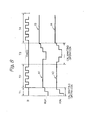
- a pre-buffer circuit receives a data signal D from an internal circuit (not shown), pull-up impedance adjusting signals RUP1, RUP2, ⁇ , RUPn and pull-down impedance adjusting signals RDN1, RDN2, ... , RDNn to generate pull-up signals P1, P2, ⁇ , Pn and pull-down signals D1, D2, ⁇ , Dn.
- the pull-up signals P1, P2, ⁇ , Pn and the pull-down signals D1, D2, ... Dn are supplied to a main-buffer circuit 2 which, in turn, generates an output signals at the output terminal OUT.
- the pull-up impedance adjusting signals RUP1, RUP2, RUPn and the pull-down impedance adjusting signals, RDN1, RDN2, ..., RDNn are generated from an impedance adjusting generating circuit 3 which is constructed by a control circuit 31, a dummy pre-buffer circuit 32, a dummy main-buffer circuit 33, a comparator 34 and switches 35 and 36.
- the dummy pre-buffer circuit 32 and the dummy main-buffer circuit 33 have the same circuit configuration as the pre-buffer circuit 1 and the main-buffer circuit 2, respectively.
- the dummy pre-buffer circuit 32 receives a dummy data signal D' and pull-up impedance adjusting signals RUP1', RUP2', ⁇ , RUPn', and pull-down impedance adjusting signals RDN1', RDN2', ⁇ , RDNn' from the control circuit 31.
- the switches 35 and 36 formed by MOS transistors are controlled by the control circuit 31.
- a resistor 4 is externally connected between the output of the dummy main-buffer circuit 33 and a node of the switches 35 and 36. Note that the resistor 4 can be internally provided in the output buffer apparatus of Fig. 1. In this case, the resistance value of the resistor 4 corresponds to the characteristic impedance of a transmission line to be connected to the output terminal OUT.
- the pre-buffer circuit 1 (the dummy pre-buffer circuit 32) of Fig. 1
- the pre-buffer circuit 1 is constructed by n-stage pre-drivers 11, 12, ⁇ , In each receiving the data signal D (the dummy data signal D'), one of the pull-up impedance adjusting signals PUP1, PUP2, ⁇ PUPn (PUP1', PUP2', ⁇ , PUPn') and one of the pull-down impedance adjusting signals PDN1, PDN2, ⁇ , PDNn (PDN1', PDN2', ⁇ PDNn').
- both of the pull-up signal Pi (Pi') and the pull-down signal Ni (Ni') are never at the activating levels simultaneously.
- the main-buffer circuit 2 (the dummy main-buffer circuit 33) of Fig. 1
- the main-buffer circuit 2 is constructed by n-stage drivers 21, 22, ⁇ , 2n each receiving one of the pull-up signals P1, P2, ⁇ , Pn (P1', P2', ... , Pn') and one of the pull-down signals N1, N2, ⁇ , Nn (N1', N2', ... , Nn') from the pre-drivers 11, 12, ⁇ , in.
- the pull-up signal Pi (Pi') and the pull-down signal Ni (Ni') are never at the activating levels simultaneously, i.e., which is forbidden. Also, when the pull-up signal Pi (Pi') is high (deactivating level) and the pull-down Ni (Ni') is low (activating level), the output terminal OUT is in a high impedance (HZ) state.
- the number n of the stages of the pre-drivers 11, 12, ⁇ , 1n, i.e., the drivers 21, 22, ⁇ , 2n is predetermined to cover the range of the characteristic impedance of the transmission fluctuated by external conditions such as the environmental temperature and the external power supply voltages.
- step 609 the dummy data D' is made "0" (low).
- step 610 the switch 35 is turned ON while the switch 36 is turned OFF, thus carrying out a calibrating operation of the impedance code RDN. That is, at step 611, the impedance code RDN' is initialized at 1.
- the calibrating operation is always carried out, i.e., the impedance codes RUP and EDN are renewed and fetched by the pre-buffer circuit 1 in synchronization with the data reading operation of the pre-buffer circuit 1 and the main-buffer circuit 2, so that the output signal at the output terminal OUT may be changed in the middle of data "1" or "0", i.e., the output signal at the output terminal OUT is distorted, thus deteriorating the quality of the output signal at the output terminal OUT.
- the calibrating operation of Fig. 6 can be carried out only during an initializing operation mode period T1 and a disabling operation mode period T3 where the data D is not supplied.
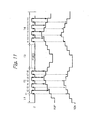
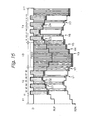
- the impedance codes RUP and RDN are not renewed, i.e., the impedance codes RUP and RDN immediately before the normal operation mode periods T2 and T4 are held as indicated by X1, X2, X3 and X4 of Fig. 8.
- the data signal D is "0" (low), while, during the disabling operation mode period T3, the data signal D is fixed at “0" (low) or "1” (high).
- the output impedance of the output buffer apparatus and the characteristic impedance of the transmission line may be suppressed, which would suppress reflection noise at the terminal of the transmission line.
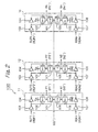
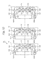
- Fig. 9 which illustrates a first embodiment of the output buffer apparatus according to the present invention
- the pre-buffer circuit 1 of Fig. 1 is replaced by a pre-buffer circuit 1A.
- Fig. 10 which is a detailed circuit diagram of the pre-buffer circuit 1A of Fig. 9, D-type flip-flops 11-1, 11-2, 12-1, 12-2, ..., 1n-1, 1n-2 are added to the elements of the pre-buffer circuit 1 of Fig. 2.
- the impedance code RUP is fetched at times t2, t4, t6, t8, 110, t12, t14, t16 by the falling edges of the data signal D.
- the impedance code RDN is fetched at times t1, t3, t5, t7, t9, t11, t13, t15 by the rising edges of the data signal D.
- the impedance codes RUP and RDN are renewed and fetched by the pre-buffer circuit 1 in synchronization with the data reading operation of the pre-buffer circuit 1 and the main-buffer circuit 2, so that the output signal at the output terminal OUT may be not changed in the middle of data "1" or "0", i.e., the output signal at the output terminal OUT is not distorted, thus improving the quality of the output signal at the output terminal OUT.
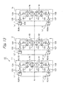
- Fig. 12 which illustrates a second embodiment of the output buffer apparatus according to the present invention
- the pre-buffer circuit 1A of Fig. 9 is replaced by a pre-buffer circuit 1B.
- Fig. 13 which is a detailed circuit diagram of the pre-buffer circuit 1B of Fig. 12, latch circuits 11'-1, 11'-2, 12'-1, 12'-2, ... , 1n'-1, 1n'-2 are provided instead of the D-type flip-flops 11-1, 11-2, 12-1, 12-2, 1n-1, 1n-2, respectively, of Fig. 10.
- the impedance code RUP is fetched at periods t2 to t3, t4 to t5, t6 to t7, t8 to t8', t10 to t11, t12 to t13, t14 to t15, t16 to t17 when the data signal D is "0" (low).
- the impedance code RDP is fetched at periods t1 to t2, t3 to t4, t5 to t6, t7 to t8, t9 to t10 t11 to t12 t13 to t14, t15 to t16 when the data signal D is "1" (high).
- the quality of the output signal can be improved, and also, reflection noise at a terminal of a transmission line connected to the output buffer apparatus can be suppressed.
Abstract
Description
Claims (4)
- An output buffer apparatus comprising:first and second power supply terminals (VDD, GND);an output terminal (OUT);a main-buffer circuit (2) including a plurality of first transistors (201) each connected between said first power supply terminal and said output terminal and a plurality of second transistors (202) each connected between said second power supply terminal and said output terminal;a pre-buffer circuit (1) including a plurality of first pre-drivers (101 to 104) each driving one of said first transistors in accordance with a data signal (D) and a plurality of second pre-drivers (105 to 108) each driving one of said second transistors in accordance with said data signal;a plurality of first sequential circuits (11-1, 12-1, ···, 1n-1 ; 11'-1, 12'-1, ···, 1n'-1), each receiving a first impedance adjusting signal (RUP1, RUP2, ···, RUPn) in synchronization with said data signal to turn ON one of said first pre-drivers; anda plurality of second sequential circuits (11-2, 12-2, ···, 1n-2 11'-2, 12'-2, ···, 1n'-2), each receiving a second impedance adjusting signal (RDN1, RDN2, ···, RDNn) in synchronization with said data signal to turn ON one of said second pre-drivers.
- The output buffer apparatus as set forth in claim 1, wherein each of said first sequential circuits comprises a first D-type flip-flop (11-1, 12-1, ···, 1n-1) for fetching said first impedance adjusting signal in synchronization with a falling edge of said data signal, each of said second sequential circuits comprising a second D-type flip-flop (11-2, 12-2, ···, 1n-2) for fetching said second impedance adjusting signal in synchronization with a rising edge of said data signal.
- The output buffer apparatus as set forth in claim 1, wherein each of said first sequential circuits (11'-1, 12'-1, ···, 1n'-1) comprises a first latch circuit which is in a hold state when said data signal indicates a first value and is in a through state when said data signal indicates a second value,
each of said second latch circuits (11'-2, 12'-2, ···, 1n'-2) comprising a second latch circuit which is in a through state when said data signal indicates said first value and is in a hold state when said data signal indicates said second value. - The output buffer apparatus as set forth in claim 3, wherein each of said first latch circuits comprises:a first transfer gate (1404) for receiving said first impedance adjusting signal, said first transfer gate being turned OFF and ON when said data signal indicates said first and second values, respectively;first and second inverters (1405, 1406) connected in a first feedback loop connected to said first transfer gate; anda second transfer gate (1407) inserted into said first feedback loop, said second transfer gate being turned ON and OFF when said data signal indicates said first and second values, respectively,each of said second latch circuits comprising:a third transfer gate (1414) for receiving said second impedance adjusting signal, said third transfer gate being turned ON and OFF when said data signal indicates said first and second values, respectively;third and fourth inverters (1415, 1416) connected in a second feedback loop connected to said third transfer gate; anda fourth transfer gate (1417) inserted into said second feedback loop, said fourth transfer gate being turned OFF and ON when said data signal indicates said first and second values, respectively.
Applications Claiming Priority (2)
| Application Number | Priority Date | Filing Date | Title |
|---|---|---|---|
| JP2002189423A JP2004032600A (en) | 2002-06-28 | 2002-06-28 | Output buffer circuit |
| JP2002189423 | 2002-06-28 |
Publications (2)
| Publication Number | Publication Date |
|---|---|
| EP1378997A2 true EP1378997A2 (en) | 2004-01-07 |
| EP1378997A3 EP1378997A3 (en) | 2004-04-28 |
Family
ID=29720217
Family Applications (1)
| Application Number | Title | Priority Date | Filing Date |
|---|---|---|---|
| EP03014638A Withdrawn EP1378997A3 (en) | 2002-06-28 | 2003-06-26 | Output buffer apparatus capable of adjusting output impedance in synchronization with data signal |
Country Status (4)
| Country | Link |
|---|---|
| US (1) | US6980019B2 (en) |
| EP (1) | EP1378997A3 (en) |
| JP (1) | JP2004032600A (en) |
| TW (1) | TW200406986A (en) |
Families Citing this family (10)
| Publication number | Priority date | Publication date | Assignee | Title |
|---|---|---|---|---|
| KR100555571B1 (en) * | 2004-09-07 | 2006-03-03 | 삼성전자주식회사 | Transmitter of semiconductor device |
| KR100640783B1 (en) * | 2004-10-30 | 2006-11-01 | 주식회사 하이닉스반도체 | Data output driver for reducing noise |
| KR100673897B1 (en) * | 2005-03-02 | 2007-01-25 | 주식회사 하이닉스반도체 | Output driver in semiconductor device |
| US7569015B2 (en) * | 2005-07-15 | 2009-08-04 | General Electric Company | Integrated physiology and imaging workstation |
| US20070016029A1 (en) * | 2005-07-15 | 2007-01-18 | General Electric Company | Physiology workstation with real-time fluoroscopy and ultrasound imaging |
| US7740584B2 (en) * | 2005-08-16 | 2010-06-22 | The General Electric Company | Method and system for mapping physiology information onto ultrasound-based anatomic structure |
| US7535250B2 (en) * | 2005-08-22 | 2009-05-19 | Micron Technology, Inc. | Output impedance calibration circuit with multiple output driver models |
| JP2013085126A (en) * | 2011-10-11 | 2013-05-09 | Elpida Memory Inc | Semiconductor device |
| KR20170080845A (en) * | 2015-12-30 | 2017-07-11 | 에스케이하이닉스 주식회사 | Data output circuit |
| CN107659280B (en) * | 2017-11-14 | 2023-10-20 | 长鑫存储技术有限公司 | Time amplifier and semiconductor memory |
Citations (3)
| Publication number | Priority date | Publication date | Assignee | Title |
|---|---|---|---|---|
| US5134311A (en) * | 1990-06-07 | 1992-07-28 | International Business Machines Corporation | Self-adjusting impedance matching driver |
| US5751161A (en) * | 1996-04-04 | 1998-05-12 | Lsi Logic Corporation | Update scheme for impedance controlled I/O buffers |
| US6166563A (en) * | 1999-04-26 | 2000-12-26 | Intel Corporation | Method and apparatus for dual mode output buffer impedance compensation |
Family Cites Families (4)
| Publication number | Priority date | Publication date | Assignee | Title |
|---|---|---|---|---|
| JP3944298B2 (en) * | 1998-02-16 | 2007-07-11 | 株式会社ルネサステクノロジ | Semiconductor integrated circuit |
| DE19825258B4 (en) * | 1998-06-05 | 2005-11-17 | Telefonaktiebolaget Lm Ericsson (Publ) | Output buffer circuit for transmitting digital signals over a preemphasis transmission line |
| JP3670563B2 (en) | 2000-09-18 | 2005-07-13 | 株式会社東芝 | Semiconductor device |
| US6922074B2 (en) * | 2002-02-07 | 2005-07-26 | International Business Machines Corporation | ASIC architecture for active-compensation of a programmable impedance I/O |
-
2002
- 2002-06-28 JP JP2002189423A patent/JP2004032600A/en active Pending
-
2003
- 2003-06-26 US US10/606,331 patent/US6980019B2/en not_active Expired - Fee Related
- 2003-06-26 EP EP03014638A patent/EP1378997A3/en not_active Withdrawn
- 2003-06-27 TW TW092117589A patent/TW200406986A/en unknown
Patent Citations (3)
| Publication number | Priority date | Publication date | Assignee | Title |
|---|---|---|---|---|
| US5134311A (en) * | 1990-06-07 | 1992-07-28 | International Business Machines Corporation | Self-adjusting impedance matching driver |
| US5751161A (en) * | 1996-04-04 | 1998-05-12 | Lsi Logic Corporation | Update scheme for impedance controlled I/O buffers |
| US6166563A (en) * | 1999-04-26 | 2000-12-26 | Intel Corporation | Method and apparatus for dual mode output buffer impedance compensation |
Also Published As
| Publication number | Publication date |
|---|---|
| EP1378997A3 (en) | 2004-04-28 |
| US20040080336A1 (en) | 2004-04-29 |
| JP2004032600A (en) | 2004-01-29 |
| US6980019B2 (en) | 2005-12-27 |
| TW200406986A (en) | 2004-05-01 |
Similar Documents
| Publication | Publication Date | Title |
|---|---|---|
| US8324925B2 (en) | Output buffer circuit and differential output buffer circuit, and transmission method | |
| US7218136B2 (en) | Transmission circuit, data transfer control device and electronic equipment | |
| US6911860B1 (en) | On/off reference voltage switch for multiple I/O standards | |
| US7973553B1 (en) | Techniques for on-chip termination | |
| US20040150447A1 (en) | Duty-cycle adjustable buffer and method and method for operating same | |
| US5486782A (en) | Transmission line output driver | |
| US7112989B2 (en) | Transmission signal correction circuit | |
| JP2003168969A (en) | Level shift circuit | |
| EP1378997A2 (en) | Output buffer apparatus capable of adjusting output impedance in synchronization with data signal | |
| US6617881B2 (en) | Semiconductor integrated circuit | |
| US7157931B2 (en) | Termination circuits having pull-down and pull-up circuits and related methods | |
| JP3708897B2 (en) | Output buffer circuit | |
| US7276939B2 (en) | Semiconductor integrated circuit | |
| US5852372A (en) | Apparatus and method for signal handling on GTL-type buses | |
| US7768311B2 (en) | Suppressing ringing in high speed CMOS output buffers driving transmission line load | |
| US7327356B2 (en) | Data transmission device and data transmission method | |
| JP2004336407A (en) | Output buffer circuit | |
| US7199616B2 (en) | Method and apparatus to generate break before make signals for high speed TTL driver | |
| US6172539B1 (en) | Synchronous buffer circuit and data transmission circuit having the synchronous buffer circuit | |
| US20050218933A1 (en) | CMOS buffer with hysteresis | |
| US6384642B1 (en) | Switched positive feedback for controlled receiver impedance | |
| JPH10224202A (en) | Buffer circuit, semiconductor integrated circuit device and electronic circuit device | |
| KR20040059440A (en) | Circiuit of output driver in semiconductor devices | |
| KR20050063203A (en) | Semiconductor memory device | |
| JPH08279743A (en) | Output pad driver |
Legal Events
| Date | Code | Title | Description |
|---|---|---|---|
| PUAI | Public reference made under article 153(3) epc to a published international application that has entered the european phase |
Free format text: ORIGINAL CODE: 0009012 |
|
| AK | Designated contracting states |
Kind code of ref document: A2 Designated state(s): AT BE BG CH CY CZ DE DK EE ES FI FR GB GR HU IE IT LI LU MC NL PT RO SE SI SK TR |
|
| AX | Request for extension of the european patent |
Extension state: AL LT LV MK |
|
| PUAL | Search report despatched |
Free format text: ORIGINAL CODE: 0009013 |
|
| AK | Designated contracting states |
Kind code of ref document: A3 Designated state(s): AT BE BG CH CY CZ DE DK EE ES FI FR GB GR HU IE IT LI LU MC NL PT RO SE SI SK TR |
|
| AX | Request for extension of the european patent |
Extension state: AL LT LV MK |
|
| RIC1 | Information provided on ipc code assigned before grant |
Ipc: 7H 03K 19/0185 B Ipc: 7H 03K 19/00 A |
|
| 17P | Request for examination filed |
Effective date: 20040317 |
|
| AKX | Designation fees paid |
Designated state(s): DE |
|
| 17Q | First examination report despatched |
Effective date: 20060921 |
|
| 17Q | First examination report despatched |
Effective date: 20060921 |
|
| STAA | Information on the status of an ep patent application or granted ep patent |
Free format text: STATUS: THE APPLICATION HAS BEEN WITHDRAWN |
|
| 18W | Application withdrawn |
Effective date: 20070523 |