-
Two further applications in magnetic random access memory array are
described in co-pending United States Patent Application number
(HP docket number 10019665-1), entitled "STYLUS BASED INPUT
DEVICES UTILIZING A MAGNETIC RANDOM ACCESS MEMORY
ARRAY", and co-pending United States Application number
(HP docket number 100200450-1), entitled "AN
INTEGRATED DIGITIZING TABLET AND COLOR DISPLAY
APPARATUS AND METHOD OF OPERATION", the disclosures of which
are hereby incorporated herein by reference
-
The present invention relates generally to digitizing input devices, for
example from the ulilization of a magnetic random access memory (MRAM)
device as a digitizing array within a digitizer apparatus that is integrated with
a display system.
-
Digitizer systems are well known to those skilled in the art. Typically, an
electro-magnetic array, or other type of system, is responsive to a stylus used by a
user to enter data directly upon a grid and to control various computer functions
by writing, sketching, or pointing the stylus against the digitizer array. Some
embodiments locate the digitizer directly on the monitor; other embodiments
separate the two devices. Usually, separate digitizers are utilized where a large
work surface is needed compared to the size of the display device such as a
monitor screen. Integrated digitizer and display devices are utilized where
portability and size are important. As such, various types of computer systems
utilize stylus-based technologies and may include portable systems, desktop
systems, transportable, or terminal-based systems.
-
The integrated digitizer-display systems are integrated only in the sense
that they are coplanar and are fitted together in a common device. They are not
integrated in that a signal processor is required to convert the signals generated
by the digitizer into display signals compatible with the display. Thus, additional
circuitry and complexity are involved in even the simplest of digitizer-display
systems that are integrated for direct input on the same display surface where the
digitizer is located.
-
Several types of stylus input digitizing devices exist in the prior art. One
type involves direct contact of a stylus tip against a capacitive-resistive array. As
the stylus tip, such as a metal tip or even a user's finger, is placed proximate a
selected area of a digitizing pad, a capacitive-resistive circuit within the pad
detects the placement of the stylus and computes its location according to well-known
mathematical formulas of a grid-based array. Typically, the capacitive-resistive
array is used over small areas in devices such as a portable digitizer
screen or finger-sensitive mouse pad.
-
A second prior art system utilizes an electromagnetic digitizer that
interacts with a magnetic-tipped stylus or electromagnetic field-generating stylus
in entering data and performing actions desired by the user. The tip of the stylus
interacts with the field on the digitizer to convey information and data from the
user. Typically a grid of intersecting lines produces a field that can be either
actively or passively modified by the field generated by the stylus. Crossing lines
can sense the field of the tip to generate a responsive signal, or can produce a
field altered by the stylus during interaction.
-
Another embodiment is that of a stylus having an RF transmitter to send
signals to the digitizing array, which then detects the transmitted signals utilizing
receiving circuits in the array. Alternatively, the pad locations may be coated and
the RF signal generated by the stylus interact with the array and are received at a
receiver within the stylus itself.
-
Further, an alternative embodiment may incorporate a light source, such
as visible or infrared light placed within the tip of the stylus to reflect off the pad.
The stylus uses an imaging device, such as a CCD camera, to detect optically the
return signal, and hence the location where the stylus interacts with the digitizer.
The system then processes and decodes the received signal and location in order
to determine the appropriate information.
-
Each of these systems has had some success; however, each has
limitations that make them difficult or undesirable to use. For example, the direct
contact technology is subject to scratches and wear during normal operation and
has low durability compared to other technologies.
-
The wire-grid electromagnetic technology is expensive to implement and
requires many individual wires for greater resolution. Additionally, the electromagnetic
digitizers typically require a planar magnetic material behind the wire-grid
sensor to shield the system from stray magnetic effects. In portable uses,
this makes the technology for the system implementing such technology heavier
than necessary. In the light-based systems, the stylus needs to be corded to the
digitizer array and the need for sophisticated electronics for producing the light
source as well as the CCD camera must be incorporated and expanded to achieve
such a stylus.
-
One disadvantage common to all the various types of prior art digitizing
technologies is that the digitizing array must always be under power in order for
interaction of the user's stylus with the digitizer to be maintained. Further, the
user must also save the information to long-term storage, such as the hard disk
drive on the computing system, in order to preserve the content of the user's
stylus session. Furthermore, in portable devices, the same can be said that the
user's input must be stored in long-term memory and cannot be maintained on the
digitizer, typically which is overlayed with the displayed system so that the user
can keep the most recent information upon restart of the apparatus unless power
is provided to preserve the information in memory.
-
Digitizing arrays have been mated with display systems in order to
provide an easy method of drawing and viewing the results simultaneously. For
example, a digitizing array may be overlayed with an indium tin oxide display
panel such that if the user interfaces with the digitizer using the stylus, the images
displayed immediately under the stylus as the user interacts therewith. This
enables the user to interact with the screen as if interacting with real data or
writing on an actual writing tablet using a pen. Such technologies always require
the use of an input signal processor, which coordinates with the digitizer to
receive the user's input via electromagnetic pulses, light pulses, resistive
interaction or the used system to process the signals for display on the display
apparatus portion.
-
The present invention seeks to provide an improved digitizing system.
-
According to an aspect of the present invention, there is provided an
integrated digitizing tablet and display as specified in claim 1.
-
According to another aspect of the present invention, there is provided
a method of converting user input to image data as specified in claim 5.
-
According to another aspect of the present invention, there is provided
an integrated digitizing and display cell as specified in claim 8.
-
The preferred embodiment can provide improved digitizing apparatus
that has greater resolution than the prior art systems, is easier to manufacture,
and is more durable during actual use. They can also provide digitizer
apparatus that can be integrated with a display device and that can be
manufactured with such a
display as an electroluminescence apparatus using the same processing methods
and techniques.
-
The preferred embodiment provides an integrated digitizing tablet and
display apparatus in which the digitizing tablet portion of the apparatus is
comprised of an array of magnetic random access memory (MRAM) cells,
wherein each MRAM cell is responsive to an externally applied magnetic field.
Each memory cell has a magnetic bit that changes orientation upon application of
an externally applied magnetic field to produce an electrical signal based on the
orientation of the bit when a second electric field is applied across the array. The
display is comprised of an array of pixel cells wherein each pixel cell is coupled
to one of the MRAM cells and is activated by the electrical signal produced by
the MRAM cell coupled thereto. Thus, what is achieved is an integrated
digitizing tablet and display wherein the digitizing cells directly control the
display cells without the need for additional processors. Further, the magnetic
field may be either a fixed or varied field as generated by the interaction of a
stylus that has either a fixed-field tip or a current-carrying tip to provide a
varying field. Further still, the stylus may interact with the MRAM array to
indicate an action to be performed by a computer system typically associated
with the integrated digitizing tablet and display. The actions typically are those
known in the art such as a right mouse click, a left mouse click, or other select
functions and features. In one embodiment, the display portion is a thin film
transistor display, but other transistor-based display systems may also be
implemented.
-
There is preferably also included a method of converting user input
into image data within the integrated digitizing tablet and display, which
includes providing an integrated array of MRAM
cells and pixel cells, each MRAM cell having a magnetic bit that changes
orientation upon application of a magnetic field and each cell being further
coupled to one pixel cell, applying a magnetic field to the array to change the
magnetic bit orientation of at least a portion of the MRAM cells, applying an
input electric signal to the array, and activating the pixel cells coupled to the
affected MRAM cells to display an image. The method may also include the
application of a second magnetic field, independent of the first magnetic field, to
change the magnetic bit orientation of at least a second portion of the MRAM
cells to offer greater flexibility or to enable a second user to interact with the
display digitizing assembly in concert with the first user. More than two
magnetic fields may be applied and processed independently of one another.
-
An additional embodiment of the present invention includes an integrated
digitizing and display cell. This integrated cell includes an MRAM cell actively
coupled to a display pixel cell, wherein the functionality of the MRAM cell
controls the functionality of the display cell directly without the need for further
processing of the contents of the MRAM cell.
-
Embodiments of the present invention are described below, by way of
example only, with reference to the accompanying drawings in which:
- Figure 1 illustrates a schematic diagram of an embodiment of
digitizing system with display unit;
- Figure 2 illustrates a schematic diagram of a stylus interaction leaving
a trace on a magnetic random access memory (MRAM) digitizing pad of that
from Figure 1;
- Figure 3 depicts a schematic diagram of an array of MRAM cells as
controlled by the sense and bit lines;
- Figure 4 depicts a cross-sectional side view of the stylus interacting
with the digitizer tablet in accordance with the tablet of Figure 2;
- Figure 5 is a diagram of the method steps utilizing inputting
information for display within the MRAM digitizer system;
- Figure 6 illustrates a schematic diagram of an embodiment of a
digitizer overlayed by a display apparatus;
- Figure 7 depicts a cross-sectional side view of an embodiment of
operation of the MRAM digitizer tablet along with a display placed on its
surface;
- Figure 8 illustrates a schematic diagram of an embodiment of electrical
circuit array utilized where MRAM cells are provided;
- Figure 9 illustrates a cross-sectional diagram of a MRAM cell fabricated
with an electroluminescence pixel according to a schematic diagram of Figure 7;
- Figure 10 illustrates an alternative embodiment of the MRAM cell
interacting with an electroluminescence pixel where the MRAM cell is located
beneath the pixel;
- Figure 11 illustrates a schematic diagram of an alternative embodiment
of utilizing an MRAM for activating a pixel; and
- Figure 12 illustrates a schematic diagram of an alternative embodiment
of a memory cell implemented to activate a pixel.
-
-
One of ordinary skill in the art would readily recognize that the
principles disclosed herein in connection with certain embodiments are equally
applicable to many types of digitizer systems with displays.
-
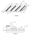
An embodiment of digitizing apparatus that connects to a display
system is illustrated in Figure 1. A digitizer 100 is disclosed
that utilizes an array of magnetic random access memory (MRAM) cells to
function as a stylus-based input device. Digitizer 100 couples to a signal
processor 102, which further connects to a display system 104. Signal processor
102 receives signals from the digitizer 100 and processes them for display on
video display 104. Digitizer 100 further includes control logic 105 that is utilized
to control digitizer 100 during operations such as array read, array write, and
array clear, which are well known to those skilled in the art.
-
Digitizer 100 is shown in further detail in Figure 2, which illustrates a
trace of a stylus tip over the surface of digitizer 100. The digitizer 100 is
composed of an array of memory cells 106. Each memory cell has at least two
state possibilities based on the orientation of a magnetic bit found within the cell
108. As a trace of a stylus interacting with the surface of digitizer 100 occurs, the
bit within the cell is reoriented causing the state of memory cell(s) 106 to change
as shown in cell 108. The trace 110 illustrates a path taken by the stylus. An
electrical signal is then applied to the array of cells 106 as a read signal to
generate a read output of those cells modified by the bit change. The read output
signal, which is a modified electric signal caused by the changed bit positions, is
then sent to the signal processor 102 of Figure 1 where it is processed according
to the pattern traced by the user. The trace 110 is then displayed on display unit
104.
-
MRAM cells have emerged as an alternative to long-term storage and the
MRAM cells have similar properties of fast access of semiconductor memory.
They can serve as long-term storage devices since they have the ability to store
information indefinitely. An MRAM cell stores a bit of information based on the
magnetic orientation of magnetization placed in a patterned thin-film magnetic
element. This magnetic film is designed so that it has two stable and distinct
magnetic states. The stable magnetic states define a binary one (1) or a binary
zero (0). Although the digital information is stored in a thin magnetic film, many
layers of very carefully controlled magnetic and dielectric layers are associated
with a memory element.
-
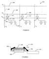
One example of an MRAM cell utilizes spin-tunneling effects and is
known as a spin-tunneling device. Figure 3 illustrates a schematic diagram of
such an MRAM cell 106. MRAM cell 106 includes a tunneling barrier layer 300,
a data storage or sense layer 302, and a reference film or pinned layer 304. The
pinned layer 304 has a magnetic orientation that is fixed so as not to rotate in the
presence of an applied magnetic field in the range of interest. The sense layer
302 has a magnetic orientation that is variable between a state aligned with the
state of the pinned layer 304 and a state in misalignment with the state of the
pinned layer 304. These orientations correspond to a low resistance state and a
high resistance state, respectively. An insulating tunnel barrier layer 300
sandwiches between the magnetic pinned layer 304 and the magnetic sense layer
302. The insulating tunnel barrier layer 300 allows quantum mechanical
tunneling to occur between the sense layer 302 and the pinned layer 304. The
tunneling is electron-spin dependent, causing the resistance of the memory cell to
vary as a function of the relative orientations of the magnetizations of the sense
layer and the pinned layer.
-
The magnetic state of a selected memory cell 106 may be changed by
applying currents to a word line 308 and a bit line 310 crossing the selected
memory cell 106. The currents produce two orthogonal magnetic fields that,
when combined, will switch the magnetic orientation of the selected memory cell
100 between the aligned and misaligned states, also known as the parallel and
anti-parallel states, respectively. Other unselected memory cells receive only a
magnetic field from either the word line or the bit line crossing the unselected
memory cells. The single field is not strong enough to change the magnetic
orientation of the unselected cells, so they retain their magnetic orientation.
When a stylus having a magnetic tip is placed proximate the cells, a sufficient
field is then applied to cause the magnetic state of the cell to change. This results
in a change of orientation between the parallel and the anti-parallel states.
-
One advantage of utilizing MRAM cells other that of the prior art is that
MRAM cells hold their orientation indefinitely without any external force applied
to them. This means that no electric field or electric current must be applied to
the MRAM cell in order to maintain the magnetization orientation of its magnetic
bit. Thus, should the device be turned off, the orientation last impressed upon the
cell will be maintained indefinitely. Once the system is reenergized, a readout
operation would signal that the state has been maintained and thus an orientation
is preserved. This allows a signal to be sent that would signify to the signal
processor and therefore displayed on the display device the previous drawing
made by the user on the digitizer array before the power was turned off.
-
The system utilizes a stylus with a magnetic tip in one embodiment that
can be scanned over the digitizer array. Beneath the surface of the pad lies an
array of MRAM cells very similar to the MRAM architecture previously
described. As the stylus moves, a magnetic field is generated by the magnet
within the tip of the stylus to cause bits to flip in the path of the stylus movement
and leaves a trace as shown in Figure 2. The MRAM array is continuously read
and scanned for changes in the bit patterns recorded in it. As the stylus moves
across the array, the trace changes the pattern and its path is displayed on the
display.
-
In one embodiment, the stylus tip shown in Figure 4 comprises a
permanent magnet that produces a known field. The magnet may be placed in the
tip used to interact with the tablet or the stylus may be coated with a magnetic
material that generates a magnetic field that can affect the MRAM memory cells.
Supporting drive electronics are found within the digitizer and are well known to
those skilled in the art. Initially, the drive electronics set all bits in the array of
memory cells in a first direction. As the stylus tip moves across the array, the
magnetic field induces a bit change in a direction opposite of their original
alignment. The drive electronics periodically may reset all bits to their original
orientation or when directed to by the user.
-
In an alternative embodiment, the tip of stylus 112 may produce a varying
magnetic field using a current carrying coil. Since the current may be altered by
changing its direction and its strength, the affected bits within the memory cells
will be placed in a unique pattern as they have been changed both in space and in
time in response to the current pattern selected by the user with the stylus. The
current pattern may be varied by the user pressing the tip downward against the
array, which may signify a button-press operation such as that on a mouse-type
pointing device, or selecting one or more buttons on the stylus, which may
signify different key clicks such as those in a mouse being a right, left, or middle
button selection. In yet another embodiment, the varying current pattern may
also signify changing colors, which will be described in greater detail below.
-
Additionally, since the MRAM cells operate independently of the other
cells and the stylus, more than one stylus may also be utilized. Accordingly, a
plurality of stylus may be utilized, each operating independently of the other as
the cells they affect also operate independently of one another. Thus, the use of
one stylus as illustrated is but exemplary of the invention and not limiting. For
example, a multi-fingered input system may be implemented. The multi-fingered
input device may be implemented within a glove array wherein each finger has a
distinctly coded stylus to generate a select signal unique from the other signals.
The multi-fingered input system would enable one user to produce multiple traces
on the underlying MRAM sensor array.
-
The magnetic cell array is sensitive to magnetic fields. The strength of
the magnetic field produced by the stylus is selected to be sufficient enough to be
detected by the array without direct contact. This allows a covering to be placed
on the top surface of MRAM cells such that the pad may be written upon directly
without fear of scratching or damaging the screen or array surface below.
-
Figure 5 illustrates a flow diagram of a method that utilizes the array of
MRAM cells as a digitizer device.
Initially, as shown in block 500, an array of such memory cells is formed. The
memory cell includes additional control logic to identify particular locations on
the digitizer panel where the stylus interacts. The detection of the stylus
interaction of changing the bit orientation within selected cells enables a signal to
be sent to a signal processing unit, which then causes the trace to be displayed on
a display apparatus. Once the MRAM
cell array has been obtained, the user then applies a magnetic field to the cells
within the array, as shown in block 502, via a stylus in order to generate a trace
line on the display.
-
Next, the system applies a read electric signal to the array, shown in block
504, in order to determine which memory cells the user has altered via the stylus
application. This electric signal, as modified by the affected cells, is forwarded
to the signal processor where it is processed so as to identify those cells that have
been modified. Once the cells are identified, pixels on the screen that correspond
to the cell location on the digitizer are then activated to reproduce the trace on the
display. During the interaction of the stylus with the digitizer panel, the system
determines if the user has performed a particular action as shown in block 506. If
the user is merely applying a magnetic field to the MRAM array, then the system
as shown on block 508, reads the output signal from each signal. Otherwise, if
the system detects that the user has performed a desired action, the system, as
shown in block 510, performs the action requested by the user. Typically, these
actions are similar to the action the user may take with a pointing device such as
a mouse or roller ball. The actions can include a right or left mouse click or a
center mouse click. The execution of a program or opening of a web page can
also be conveniently located within an operating range of the stylus as
implemented by the user.
-
Lastly, once the array has had its electric signal applied to it and the
output signals have been read from each cell, the signal processor, as shown in
block 512, processes the output electric signals and displays an image on the
display corresponding to the image data discerned from the output electric signal.
It should be noted that the output electric signal can provide output for more than
one trace performed on the digitizer at any time as well as that different colors
may be used for different traces or stylus actions as contemplated within the
invention.
-
Another embodiment of the present invention is illustrated in Figure
6. A display panel 104 physically mated with a digitizing MRAM array 100 is
illustrated in the schematic diagram of Figure 6. Display 104 is placed over
digitizer 100 such that as the user traces the stylus across the surface of display
104, the magnetic field interacts with the array 100 below and causes a trace to be
drawn exactly where the stylus interacts with the display panel. Signals are sent
to the signal processor 102 and then sent to the display panel 104 for display.
This has the advantage of integrating a digitizing apparatus 100 with a display
apparatus 104 such as are utilized on laptop computers and personal digital
assistances (PDA) devices and the like.
-
Another embodiment of the invention, as illustrated in Figure 7, mates a
display apparatus 104 with a digitizer apparatus 100 such that the digitizer,
utilizing the MRAM cells, actively controls the display pixels found within a
display panel 104. The display panel used in this type of system typically utilizes
transistors such as in an active matrix and is well known to those skilled in the
art. The MRAM cells in the array are mated with a selected transistor to activate
the pixel within the display.
-
Figure 8 illustrates a schematic diagram of an array of pixels as controlled
by a memory cell as integrated in a single digitizer-display system 200. Each
pixel 202 is represented in the contents located within the dotted block and also
contains a pixel enable line 206, a first row memory cell voltage line 208, and a
second row memory cell voltage line 210.
-
Each display pixel 202 includes an MRAM cell 212, fixed between the
two row memory cell voltage lines 208 and 210. Voltage cell line 210 is then
further coupled to a switching device 214, such as a field effect transistor, which
has its source coupled to the pixel enable line 206. Transistor 214 controls a
pixel diode 216. In this illustration, pixel diode 216 generates a light of red color
with a series of red, green, and blue pigments being provided in adjacent pixels to
provide a color display and to depict an implementation of an MRAM array
digitizer controlling a color apparatus and providing distinct color selection
through the use the stylus. Each pixel 216 is coupled to a capacitor 218, to
provide a constant power source to the pixel 216 when it is active.
-
The array 200 of Figure 8 illustrates three pixels, selected from red, green,
and blue (RGB). The array actually comprises a plurality of the pixels, with three
colors being grouped together in individual cells comprising a single color pixel
and a single MRAM. Thus, the array comprises a plurality of color pixels formed
in an RGB matrix. Although there is illustrated an equal number pixels for each
color, it should be noted that it is intended that the intensity level of each color be
generally equal. As such, the designer will add additional pixels of one color
over another in order to achieve equal color intensity. Or, the intensity of each
color pixel can be controlled by another memory cell so that only one pixel per
color is planned.
-
The array can comprise anywhere from just a few pixels in the X and Y
directions to as large as is necessary to supply a display apparatus of conventional
size. Such a display would have over a thousand lines in both the X and the Y
dimensions.
-
Figure 9 illustrates a cross-sectional view of a cell 202 as implemented in
a semiconductor material. The MRAM cell 212 is fabricated in the semiconductor
material adjacent a light emitting pixel 216. The switch 214, which
includes a source connection 218 and a drain connection 220, connects to pixel
216 for activation. A gate 222 is formed below the MRAM cell 216. The cell
also includes proper isolation and conductive layers necessary for patterning and
manufacturing an MRAM cell as well as a display pixel.
-
Figure 9 further illustrates that the control cell portion is placed adjacent
the display cell 216. The magnetic switching cells are typically much smaller
than the display pixels. As such, the MRAM cells can be fabricated adjacent the
display pixels since the display pixels are generally at least one order of
magnitude larger than the MRAM cells. For example, the MRAM cells have a
form factor ranging from 0.2 to 2.0 microns while the display pixels have a form
factor of at 4 or 5 microns or larger. As such, additional control switches may be
utilized because of their size and can serve as brightness control, among other
needs.
-
Placing the memory cell adjacent the pixel uses more semiconductor
surface area than placing the memory cell below the pixel. Thus, an alternative
embodiment of locating the memory cell 212 below the pixel display cell 216 is
shown in Figure 10. This enables greater resolution and greater density to be
achieved in the same surface area as that of the pixel array shown in Figure 9.
The memory cells are displaced but a small distance behind or below the pixels.
The distance is slight enough that the stylus can still interact with the memory
cells when moved across the top surface of the digitizing display. This increased
pixel density is not possible using other technologies that place the switch within
the same substrate as the pixel. This displacement also makes the magnetic cells
less susceptible to outside magnetic fields, which will typically attenuate before
affecting the orientation of the bit within a given memory cell.
-
Figure 11 illustrates yet another embodiment of a directly activated
display pixel 216, wherein memory cell
212 controls the source of the switching transmitter 214 as opposed to being
connected directly to the gate as was illustrated in Figure 8. The array includes a
first column memory voltage control line 232 and a second column memory
voltage line 234, which connect in parallel with memory cell 212. A pixel row
control line 236 couples to the gate of transistor 214. When a signal is applied to
voltage line 232, a current flows through memory cell 212 depending upon the
orientation of the bit therein. If the orientation allows for current flow through
the cell, then switch 214, activated by control line 236, causes pixel 216 to
activate and display. Additional cells are provided to form an array of cells.
-
Figure 12 illustrates yet another embodiment that utilizes a
memory cell 212 in an improved circuit for controlling the activation of a display
pixel 216. A pair of memory cells 212 controls the activation of switching
transistor 214. The pair of memory cells 212 is placed within a differential sense
amplifier circuit to determine the signal strength of either an activated or non-activated
memory cell using conventional means. A first cell 212 receives a first
signal and the second cell receives a second signal complementary to the first
signal. The use of complementary cells is exemplary only and is utilized as it
improves the signal-to-noise ratio of the sensing electronics. Alternatively, a
single cell can be utilized that is not dependent on a complementary cell for
improved noise reduction or accuracy.
-
Further, the cell size is scalable depending upon the accuracy desired as
well as the display device integrated within the digitizing system. For example,
current processing techniques yield cell sizes ranging from 0.1 micron to 0.3
micron in memory array applications. For applications in display and digitizer
systems, cell sizes comparable with the display pixel and switching circuit sizes
is acceptable, which provides sizes in the micron to the tens of microns size. This
scalability provides yet another advantage over that of the prior art.
-
Thus, it has been demonstrated that a digitizing device utilizing an array
of MRAM cells may be incorporated to interact with a display device and that the
digitizer device may actually be combined with the display using thin-film
transistor cells so the memory cells directly activate the pixels within an active
matrix display. The result is a digitizer-display that needs little, if any, signal
processing logic as is required in other digitizer-display units. Thus, as the user
writes a trace directly on the display, the trace is displayed directly on the screen
with little, if any, intermediary processing.
-
Further, since the MRAM cells array serves as an addressable memory
array, this simplifies the drive electronics typically required in prior art systems.
Additionally, the displayed image/graphics or otherwise defined information can
be stored in a non-volatile fashion due to the nature of the MRAM cells as
previously described. Since the MRAM cells retain the last selected orientation
of the memory bits indefinitely, when the display system is turned off and then
turned on again, no loss of information occurs. The display acts as a writable and
reusable paper medium rather than as a conventional digitizer tablet that always
required saving of data to a long-term memory store rather than directly within
the digitizer itself.
-
Although thin-film transistor (TFT) cells have been depicted in the
specific embodiments of the present invention, alternative display cells may also
be utilized. In addition, the MRAM cell disclosed has utilized tunneling
magneto-resistive (TMR) effect, but other MRAM cells may also be
contemplated. These will include cells based on magneto-resistive (MR) effect,
giant magneto-resistive (GMR) effect, magnetic tunneling junction (MTJ) effect,
or colossal magneto-resistive (CMR) effect.
-
There are four very different physical effects that produce MR of different
types: AMR (anisotropic), GMR (giant), TMR (tunneling) and CMR (colossal).
Tunneling Magneto-resistance (TMR) or the tunneling magneto-resistive effect
(TMR effect) is the change in resistance generated by the physical effect of spin-dependent
tunneling (SDT) that is seen in a magnetic tunnel junction (MTJ, also
sometimes called an SDT junction).
-
For illustration, an MTJ-based cell behaves as a resistance with two states,
having a high resistance state and a low resistance state. The memory cell is
connected to the gate of the transistor switch 216 and the memory cell resistance
is chosen such that the drive voltage will turn on or off the pixel or the switch 214
depending upon the state of the memory cell 212. Once the switch 214 turns on
(or off) it causes the neumatic liquid crystal display to block (or pass) light
through it. The state of the cell 212 is changed externally by the presence of the
stylus in the magnetic field located within the tip of the stylus. This further
causes the switch 214 to turn off or on and consequently the pixel turns off or on.
-
Additionally, switching and conveying electronics is also incorporated
into the design such that the entire memory cell array may be refreshed or erased
or individual cells may be turned on or off or refreshed. Further, the electronics
allows for the information in the cells to be stored in the long-term memory
device should the contents in the array need to be saved but also erased so that
additional writings may be performed.
-
The application of color to the memory cell array can be obtained by
creating memory cells of differing levels of sensitivity. This means that the cells
for red may be sensitive to a neumatic field of a particular field strength separate
from that of the blue or green pixels and vice versa. This allows the user the
option of modifying colors on the fly by actively selecting the level of field
strength desired that would activate one, two or all three pixels at any time to
achieve the desired colored results.
-
It is to be understood that the above-described arrangements are only
illustrative of the application for the principles disclosed herein.
Numerous modifications and alternative arrangements may be devised by those
skilled in the art without departing from the scope of the appended claims.
The disclosures in United States patent application No. 10/038,466, from
which this application claims priority, and in the abstract accompanying this
application are incorporated herein by reference.