BACKGROUND OF THE INVENTION
1. Field of the Invention
-
The present invention relates to a method of
manufacturing a semiconductor device, and more
particularly to a method of manufacturing a
semiconductor device in which a barrier insulating
film for covering a copper wiring is formed by use
of a plasma enhanced CVD method.
2. Description of the Prior Art
-
Recent years, a high speed of a data transfer
speed has been desired along with a high integration
and high density of a semiconductor integrated
circuit device. Therefore, an insulating film
having a low dielectric constant with a less RC
delay (hereinafter referred to as a low dielectric
constant insulating film) has been used.
-
On the other hand, with respect to a wiring
material, a copper (Cu) wiring showing a low
electric resistivity has come to be used instead of
the conventional aluminum (A1) wiring.
-
Therefore, as an interlayer insulating film, the
low dielectric constant insulating film is formed on
the copper wiring. When the low dielectric constant
insulating film is formed after the formation of the
copper wiring, or alternatively in steps after the
formation of the copper wiring, annealing at about
400 to about 450 °C is carried out. Moreover, a high
field is applied to the interlayer insulating film
during the operation of the semiconductor device.
Accordingly, to prevent diffusion of copper into the
low dielectric insulating film owing to heat and
electric field, a barrier insulating film is
sandwiched between the low dielectric constant
insulating film and the copper wiring.
-
However, the barrier insulating film is dense
but shows a high relative dielectric constant.
Among various barrier insulating films, a SiC-based
barrier insulating film shows a relative dielectric
constant as relatively low as about 5. However,
when a thickness of a barrier insulating film having
a relative dielectric constant of 5 is made to be
100 nm relative to a low dielectric constant
insulating film having a thickness of 500 nm and a
relative dielectric constant of 2.8, a relative
dielectric constant of an interlayer insulating film
composed of the low relative dielectric constant
insulating film and the barrier insulating film
becomes as high as 3.02.
-
Therefore, it has been tried to make the
thickness of the barrier insulating film as thin as
about 50 nm. However, in this case, a capability to
prevent copper diffusion is deteriorated.
SUMMARY OF THE INVENTION
-
The present invention relates to a semiconductor
device having a barrier insulating film with a low
relative dielectric constant, which covers a wiring
formed of a copper film or mainly formed of a copper
film, and relates to a method of manufacturing the
same. An object of the present invention is to
provide a semiconductor device having a barrier
insulating film with a low relative dielectric
constant, which shows a small leak current and high
capability to prevent copper diffusion, and to
provide a method of manufacturing the same.
-
In the present invention, a film forming gas
containing an alkyl compound and an oxygen-containing
gas is supplied between first and second
electrodes, and gas pressure is regulated to 1 Torr
or less. Thereafter, high frequency power of a
frequency of 1 MHz or more is applied to any one of
the first and second electrodes, and the film
forming gas is converted into a plasma. The
plasmanized film forming gas are reacted with each
other, and a barrier insulating film covering a
copper wiring is formed.
-
The use of the film forming gas converted into a
plasma state only by the high frequency power makes
it possible to acquire a low relative dielectric
constant. Moreover, it is possible to maintain
denseness of the insulating film enough to prevent
copper diffusion by controlling the pressure of the
film forming gas to 1 Torr or less at least at an
early stage of the film formation.
-
To increase the denseness of the insulating film
while maintaining the low relative dielectric
constant thereof, the film formation is carried out
under a condition that the pressure of the film
forming gas is gradually elevated from low pressure
to 1 Torr in the present invention. Alternatively,
ammonium (NH3) and nitrogen (N2) are added to the
film forming gas at least at the early stage of the
film formation. Alternatively, a film forming gas
containing a dilution gas formed of at least any one
of He and Ar is used. Alternatively, the film
forming gas is used under a condition that a flow
rate of the dilution gas is increased at least at
the early stage of the film formation.
Alternatively, bias power of a low frequency is
applied at the early stage of the film formation.
-
Moreover, hydrocarbon is added to the film
forming gas. Thus, the formed film can be enhanced
in etching selectivity for the etchant of the
insulating film with the low relative dielectric
constant, which is formed on the barrier insulating
film.
-
As described above, according to the present
invention, the barrier insulating film having a
further low relative dielectric constant can be
formed while maintaining the denseness enough to
prevent the copper diffusion.
BRIEF DESCRIPTION OF THE DRAWINGS
-
- FIG. 1 is a side view illustrating a
constitution of a plasma enhanced CVD apparatus used
for a method of manufacturing a semiconductor device,
which is an embodiment of the present invention.
- FIGs. 2A to 2K are charts illustrating a film
forming method using particularly effective
combinations of gases and effective combinations of
film forming conditions, which are the embodiment of
the present invention.
- FIG. 3 is a graph illustrating a characteristic
of a leakage current of a silicon-containing
insulating film immediately after a film formation
(as depo.), which is formed under a film forming
condition I by a film forming method of a first
embodiment of the present invention.
- FIG. 4 is a graph illustrating a characteristic
of the leakage current of the silicon-containing
insulating film immediately after the film formation
(as depo.) and after annealing, which is formed
under the film forming condition I by the film
forming method of the first embodiment of the
present invention.
- FIG. 5 is a graph illustrating a characteristic
of a leakage current of a silicon-containing
insulating film immediately after a film formation
(as depo.), which is formed under a film forming
condition II by a film forming method of a second
embodiment of the present invention.
- FIG. 6 is a graph illustrating a characteristic
of the leakage current of the silicon-containing
insulating film immediately after the film formation
(as depo.) and after annealing, which is formed
under the film forming condition II by the film
forming method of the second embodiment of the
present invention.
- FIG. 7 is a graph illustrating a characteristic
of a leakage current of a silicon-containing
insulating film immediately after a film formation
(as depo.), which is formed under a film forming
condition III by a film forming method of a third
embodiment of the present invention.
- FIG. 8 is a graph illustrating a characteristic
of the leakage current of the silicon-containing
insulating film immediately after the film formation
(as depo.) and after annealing, which is formed
under the film forming condition III by the film
forming method of the third embodiment of the
present invention.
- FIG. 9 is a graph illustrating states of a
change of a relative dielectric constant (k) of an
insulating film relative to a gas pressure (P) of a
film forming gas, and a relationship of a dielectric
breakdown-resistance of the insulating film after
annealing with the gas pressure (P) and the relative
dielectric constant (k), for the insulating film
which is prepared under a film forming condition IV
by a film forming method of a fourth embodiment of
the present invention.
- FIG. 10 is a graph illustrating a barrier
property for copper in the insulating film prepared
under the condition IV by the film forming method of
the fourth embodiment of the present invention.
- FIG. 11 is a graph illustrating states of a
change of a relative dielectric constant (k) of an
insulating film relative to a N2O gas flow rate in a
film forming gas, and a relationship of a dielectric
breakdown-resistance of the insulating film after
annealing with the N2O gas flow rate and the
relative dielectric constant (k), for the insulating
film which is prepared under a film forming
condition V by a film forming method of a fifth
embodiment of the present invention.
- FIG 12 is a graph illustrating states of a
change of a relative dielectric constant (k) of an
insulating film relative to a He gas flow rate in a
film forming gas, and a relationship of a dielectric
breakdown-resistance of the insulating film after
annealing with the He gas flow rate and the relative
dielectric constant (k), for the insulating film
which is prepared under a film forming condition VI
by a film forming method of a sixth embodiment of
the present invention.
- FIG. 13 is a graph illustrating states of a
change of a relative dielectric constant (k) of an
insulating film relative to a N2O gas flow rate in a
film forming gas, and a relationship of a dielectric
breakdown-resistance of the insulating film after
annealing with the N2O gas flow rate and the
relative dielectric constant (k), for the insulating
film which is prepared under a film forming
condition VII by a film forming method of a seventh
embodiment of the present invention.
- FIG. 14 is a graph illustrating states of a
change of a relative dielectric constant (k) of an
insulating film relative to a NH3 gas flow rate in a
film forming gas, and a relationship of a dielectric
breakdown-resistance of the insulating film after
annealing with the NH3 gas flow rate and the
relative dielectric constant (k), for the insulating
film which is prepared under a film forming
condition VIII by a film forming method of an eighth
embodiment of the present invention.
- FIG. 15 is a graph illustrating states of a
change of a relative dielectric constant (k) of an
underlying film of two insulating films relative to
sorts of the underlying film and gas pressure (P) of
a film forming gas, for the underlying film which
are prepared under a film forming condition IX by a
film forming method of a ninth embodiment of the
present invention.
- FIG. 16 is a graph illustrating states of a
change of a relative dielectric constant (k) of an
underlying film of two insulating films relative to
sorts of the underlying film and a N2O gas flow rate
of a film forming gas, for the underlying film which
are prepared under a film forming condition X by the
film-forming method of the ninth embodiment of the
present invention.
- FIG. 17 is a graph illustrating states of a
change of a relative dielectric constant (k) of a
main insulating film of two insulating films
relative to sorts of the main insulating film and
gas pressure of a film forming gas, for the main
film which are prepared under a film forming
condition XI by the film forming method of the ninth
embodiment of the present invention.
- FIG. 18 is a graph illustrating a relationship
of a dielectric breakdown-resistance with relative
dielectric constants (k) of a underlying film and a
main insulating film concerning a two-layered
insulating film which is a combination of the
underlying film and the main insulating film
prepared under the film forming conditions IX, X and
XI by the film forming method of the ninth
embodiment of the present invention.
- FIG.19 is a sectional view of a semiconductor
device in which the present invention is applied to
a barrier insulating film covering a wiring made
mainly of copper.
-
DESCRIPTION OF THE PREFERRED EMBODIMENTS
-
Embodiments of the present invention will be
described with reference to the accompanying
drawings below.
(Description of a plasma enhanced CVD apparatus used
for a film forming method which is an embodiment of
the present invention)
-
FIG. 1 is a side view illustrating a
constitution of a parallel plate plasma enhanced CVD
apparatus 101 used for a method of manufacturing a
semiconductor device according to an embodiment of
the present invention.
-
This parallel plate plasma enhanced CVD
apparatus 101 is constituted by a film forming
portion 101A where a barrier insulating film is
formed on a substrate 21 subject to film formation
by use of a plasma gas, and a film forming gas
supply portion 101B having a plurality of gas supply
sources constituting a film forming gas.
-
The film forming portion 101A comprises a
chamber 1 in which pressure can be reduced, as shown
in FIG. 1, and the chamber 1 is connected to an
exhaustion device 6 through an exhaustion pipe 4.
An open/close valve 5 for controlling
communication/noncommunication between the chamber 1
and the exhaustion device 6 is provided in the
exhaustion pipe 4. Pressure measurement means such
as a vacuum gauge (not shown) for monitoring
pressure in the chamber 1 is provided in the chamber
1.
-
A pair of upper and lower electrodes (first and
second electrodes) 2 and 3, which oppose to each
other, are provided in the chamber 1. A high
frequency electric power supply source (RF electric
power supply source) 7 for supplying high frequency
electric power of a frequency of 13.56 MHz is
connected to the upper electrode 2. A low frequency
electric power supply source 8 for supplying low
frequency electric power of a frequency of 380 kHz
is connected to the lower electrode 3. The high
frequency electric power is supplied to the upper
electrode 2 from at least the high frequency
electric power supply source 7 of these power
sources 7 and 8, and the film forming gas is
converted to a plasma. The upper electrode 2, the
lower electrode 3 and the power sources 7 and 8
constitute plasma generation means for converting
the film forming gas into a plasma.
-
Note that not only the low frequency electric
power of the frequency of 380 kHz but also low
frequency electric power of a frequency ranging from
50 kHz to 1 MHz can be applied to the lower
electrode 3. Moreover, not only the high frequency
electric power of the frequency of 13.56 MHz but
also high frequency electric power of a frequency of
1 MHz or more can be applied to the upper electrode
2 facing the lower electrode 3. In FIG. 1, a high
frequency power source is connected to the upper
electrode 2, and a low frequency electric power
source is connected to the lower electrode 3.
However, the object of the present invention can be
achieved as long as the high frequency electric
power source 7 is connected to the lower electrode 3
or to any one of the upper and lower electrodes 2
and 3, and the lower frequency electric power source
8 is connected to the lower electrode 3 or to the
other electrode.
-
The upper electrode 2 serves also as a
dispersion head of the film forming gas. A
plurality of through holes for guiding the film
forming gas are formed in the upper electrode 2.
Each through hole is communicated to an opening
portion in the facing plane of the lower electrode 3
and the opening portion serves as a discharging port
(introduction port) of the film forming gas. The
discharging port for this film forming gas is
connected to the film forming gas supply portion
101B by a pipe 9a. A heater (not shown) may be
provided in some cases in the upper electrode 2.
The heater is provided so that particles formed of
reaction product of the film forming gas are
prevented from being adhered to the upper electrode
2 by heating the upper electrode 2 to about 100 °C
during the film formation.
-
The lower electrode 3 serves also as a holding
stage of the substrate 21. Moreover, the lower
electrode 3 comprises a heater 12 for heating the
substrate 21 on the holding stage.
-
In the film forming gas supply portion 101B,
there are provided a supply source for supplying an
alkyl compound having a siloxane bond such as
hexamethyl disiloxane (HMDSO: (CH3)3Si-O-Si(CH3)3) or
the like, a supply source for supplying methyl
silane expressed by a general formula: SiHn(CH3)4-n
(n = 0 to 3), a supply source for supplying an alkyl
compound having an O-Si-O bond, a supply source for
supplying hydrocarbon (CmHn) such as methane (CH4),
acetylene (C2H2) and ethylene (C2H4), a supply source
for supplying an oxygen-containing gas such as
oxygen (O2), dinitrogen monoxide (N2O), water (H2O),
carbon dioxide (CO2), a supply source for supplying
ammonium (NH3), a supply source for supplying an
dilution gas formed of at least any one of He and Ar
(inert gas), and a supply source for supplying
nitrogen (N2) that is also an inert gas.
-
These gases are suitably supplied to the chamber
1 in the film forming portion 101A through branch
pipes 9b to 9i and the pipe 9a connected to the
branch pipes 9b to 9i. In the respective branch
pipes 9b to 9i, there are provided flow rate
adjusting means 11a to 11h and open/close means 10b
to 10n and 10p to 10r for controlling
communication/noncommunication of the branch pipes
9b to 9i. Open/close means 10a for opening/closing
the pipe 9a is provided in the pipe 9a. Moreover,
close/open means 10s to 10x for controlling
communication/noncommunication between the branch
pipe 9i connected to the supply source of a N2 gas
and the other branch pipes 9b and 9g are provided in
order to purge a residual gas in the branch pipes 9b
to 9g by allowing the N2 gas to flow therethrough.
Note that the N2 gas is used also for purging a
residual gas in the pipe 9a and the chamber 1 as
well as in the branch pipes 9b to 9g. Moreover, the
N2 gas is in some cases used as the film forming gas.
-
According to the film formation apparatus 101 as
described above, there are provided the supply
source for supplying the alkyl compound having the
siloxane bond such as hexamethyl disiloxane (HMDSO),
the supply source for supplying methyl silane
expressed by general formula: SiHn(CH3)4-n (n = 0 to
3), the supply source for supplying the alkyl
compound having the O-Si-O bond, the supply source
for supplying hydrocarbon (CmHn), the supply source
for supplying the oxygen-containing gas such as
oxygen (O2), dinitrogen monoxide (N2O), water (H2O),
carbon dioxide (CO2), the supply source for
supplying ammonium (NH3), the supply source for
supplying the dilution gas formed of at least any
one of He and Ar (inert gas), and the supply source
for supplying nitrogen (N2) that is also an inert
gas. Moreover, plasma generating means 2, 3, 7 and
8 for converting the film forming gas into a plasma
are provided.
-
Thus, it is possible to form a barrier
insulating film with a low dielectric constant and
high denseness, which is capable of suppressing
copper diffusion, by use of a plasma enhanced CVD
method described below.
-
FIG.19 is a sectional view of a semiconductor
device in which the above film forming method is
applied to a barrier insulating film covering a
wiring made mainly of copper. In FIG.19, films
denoted by symbols 35a, 39 are the barrier
insulating films covering a lower wiring and upper
wiring made mainly of copper, respectively.
-
In the semiconductor device, there are laminated a
lower wiring berried insulating film 32, an inter
wiring layer insulating film 35 and an upper wiring
berried insulating film 36 on the substrate 31. The
wiring berried insulating film 32, 36 both are
formed of a low dielectric insulating film, and the
inter wiring layer insulating film 35 is formed of a
two-layered structure of the barrier insulating film
and a low dielectric insulating film.
-
The lower wiring 34 is berried in a wiring trench
32a of the wiring berried insulating film 32, and
the upper wiring 38 is berried in a wiring trench
36a of the wiring berried insulating film 36. The
lower wiring 34 and the upper wiring 38 are
connected with each other by a connection conductor
37 berried in a via hole 35a formed through the
inter wiring layer insulating film 35. The lower
wiring 34, the connection conductor 37 and the upper
wiring 38 are formed of main copper films 34b, 37b,
38b, and barrier metal films 34a, 37a, 38a which
protect lower parts and side portions of main copper
films 34b, 37b, 38b. The barrier insulating films
35a, 39 cover the upper surfaces of the copper films
34b, 38b, respectively.
-
Next, there will be made descriptions for an
alkyl compound having a siloxane bond, methyl silane,
an alkyl compound having an O-Si-O bond, and
hydrocarbon, which are the film forming gas of the
barrier insulating film used for the present
invention.
-
The following can be used as the representative
example.
- (i) alkyl compound having a siloxane bond
- hexamethyldisiloxane (HMDSO: (CH3)3Si-O-Si(CH3)3)
- octamethylcyclotetrasiloxane (OMCTS)
- tetramethylcyclotetrasiloxane (TMCTS)
- octamethyltrisiloxane (OMTS)
- (ii) methyl silane (SiHn(CH3)4-n: n = 0 to 3)
- monomethylsilane (SiH3(CH3))
- dimethylsilane (SiH2(CH3)2)
- trimethylsilane (SiH(CH3)3)
- tetramethylsilane (Si(CH3)4)
- (iii) alkyl compound having an O-Si-O bond
- compound having a structural formula of CH3-O-Si(CH3)2-O-CH3
- (iv) hydrocarbon (CmHn)
- methane (CH4)
- acetylene (C2H2)
- ethylene (C2H4)
-
(Description of a film forming method of an
embodiment of the present invention)
-
Next, a film forming method using a particularly
effective combination of gases and an effective
combination of film forming conditions, which is the
embodiment of the present invention, will be
described with reference to FIGs. 2A to 2K.
-
These drawings are charts illustrating a timing
of an introductions of each gas composing the film
forming gas into the chamber 1, conditions of a gas
flow rate and gas pressure during the film formation,
and a method of applying high frequency power and
low frequency power applied to two electrodes of
parallel plate type during the film formation.
-
Among these drawings, FIGs. 2A to 2E illustrates
the charts of the method of forming a silicon-containing
insulating film by use of a film forming
gas composed of at least an alkyl compound and an
oxygen-containing gas.
-
In FIG. 2A, the pressure of the film forming gas
introduced into the chamber 1 is regulated to 1 Torr
or less, and high frequency power is applied to any
one of the lower and upper electrodes 2 and 3, thus
converting the film forming gas into a plasma state.
The chart of FIG. 2B differs from that of FIG. 2A in
that the film formation is carried out while
increasing the pressure of the film forming gas from
low pressure to 1 Torr gradually. The chart of FIG.
2C differs from that of FIG. 2A in that the pressure
of the film forming gas introduced into the chamber
1 is regulated to 1 Torr or less for a certain
period of time at the early stage of the film
formation, and then regulated to a higher pressure
than 1 Torr after passage of the certain period of
time. The chart of FIG. 2D differs from that of FIG.
2A in that high frequency power is applied to any
one of the upper and lower electrodes 2 and 3 and
low frequency power is applied to the other
electrode for a certain period of time at the early
stage of the film formation. The chart of FIG. 2E
differs from that of FIG. 2A in that the flow rate
of the oxygen-containing gas of the film forming gas
is made to be high for a certain period of time at
the early stage of the film formation and is made to
be low after passage of the certain period of time.
-
Moreover, in FIGs. 2F to 2K described below, on
the assumption that the gases shown in the drawings
are composed by adding these gases to other gases,
only conditions under which each of the gases is
added to other gases are illustrated.
-
FIGs. 2F to 2H are charts when the film
formation is carried out by use of a film forming
gas containing dilution gas.
-
In FIG. 2F, the dilution gas of an ordinary flow
rate is added. The chart of FIG. 2G differs from
that of FIG. 2F in that the flow rate of the
dilution gas is increased. The chart of FIG. 2H
differs from that of FIG. 2F in that the flow rate
of the dilution gas is increased for a certain
period of time at the early stage of the film
formation and, then, is lowered after passage of the
certain period of time.
-
FIGs. 2I to 2J are charts when the film
formation is carried out by use of a film forming
gas containing at least any one of an ammonium gas
and a nitrogen gas.
-
In the chart of FIG. 2I, at least any one of the
ammonium gas and the nitrogen gas is added through
the entire period of the film formation. The chart
of FIG. 2J differs from that of FIG. 2I in that at
least any one of the ammonium gas and the nitrogen
gas is supplied only for a certain period of time at
the early stage of the film formation.
-
The combinations of the gases illustrated in
FIGS. 2F to 2K and other gases are realized by the
following methods (a) to (c). (a) The gas of FIGs.
2B, 2D or 2E and any one of gases of FIGs. 2F to 2K
can be combined. (b) The gas obtained by combining
the gas of FIGs. 2B, 2D or 2E with any one of the
gases of FIGs. 2F to 2H can be combined with any one
of gases of FIGs. 2I to 2J. Moreover, (c) each gas
obtained as a result of the combinations of (b) can
be combined with the gas of FIG. 2K.
-
By use of the film forming gas which is
converted into a plasma state only by the high
frequency power, a low relative dielectric constant
can be achieved. Furthermore, it is possible to
maintain denseness of the insulating film enough to
prevent copper diffusion by controlling the pressure
of the film forming gas to 1 Torr or less at least
at the early stage of the film formation.
-
By forming the film while gradually increasing
the pressure of the film forming gas from low
pressure to 1 Torr, a dense film can be obtained at
the portion closer to the wiring or the electrode
mainly formed of the copper film, and a film with a
lower dielectric constant can be obtained as the
film is apart from the wiring or the electrode.
-
Moreover, the denseness can be enhanced by
adding ammonium (NH3) or nitrogen (N2) to the film
forming gas at least at the early stage of the film
formation, or by using the film forming gas
containing the dilution gas composed of He, or by
using the film forming gas increasing the flow rate
of the dilution gas at least at the early stage of
the film formation, or by applying bias power of the
low frequency at the early stage of the film
formation.
-
Moreover, by adding the hydrocarbon, it is
possible to enhance an etching resistance to an
etchant of the low dielectric constant film formed
on the barrier insulating film.
-
As described above, the film formation is
carried out by use of a plasma enhanced CVD method
to which the present invention is applied according
to the foregoing chart, whereby it is possible to
form the barrier insulating film which is dense
enough to prevent the copper diffusion and has a low
relative dielectric constant.
-
Next, there will be described results of
examinations of the relative dielectric constant and
leakage current of the silicon-containing insulating
film, which is formed under various film forming
conditions by the method of manufacturing a
semiconductor device to which the present invention
is applied by use of the foregoing plasma enhanced
CVD apparatus.
- (1) First embodiment
As a sample, after a surface oxide film on a
copper film was removed by a treatment prior to a
film formation, a silicon-containing insulating film
was formed on the copper film. The silicon-containing
insulating film was formed under the
following film forming conditions by use of a plasma
enhanced CVD method.
-
(Treatment prior to film formation)
-
- (i) treatment gas: NH3
- gas flow rate: 500 sccm
- gas pressure: 1 Torr
- (ii) condition for plasma formation
- frequency: 13.56 MHz
- power: 100 W
- time: 10 seconds
- (iii) substrate heating temperature: 375 °C
-
(Film forming condition I)
-
- (i) condition of film forming gas
- HMDSO flow rate: 50 sccm
- N2O flow rate: 400 sccm
- He flow rate: 400 sccm
- gas pressure: 1 Torr
- (ii) condition for plasma formation
- high frequency power (13.56 MHz) PRF: 250 W
- low frequency power (380 KHz) PLF: 0 W
- (iii) substrate heating temperature: 375 °C
- (iv) formed silicon-containing insulating film
- film thickness: 100 nm
- relative dielectric constant: 2.89
-
(Annealing condition)
-
- temperature: 450 °C
- treatment time: 4 hours
-
-
In the measurement of the relative dielectric
constant, a mercury probe having an electrode area
of 0.0226 cm2 was allowed to touch the surface of
the silicon-containing insulating film. Then, a DC
bias voltage was applied to the mercury probe along
with a small signal voltage of 1 MHz. The relative
dielectric constant was obtained by performing a
conversion from the measured C-V characteristics.
-
Moreover, in the measurement of the leakage
current and the dielectric breakdown-resistance, the
copper film was grounded and a negative voltage was
applied to the mercury probe.
-
The results obtained by measuring the leakage
current and the dielectric breakdown-resistance are
shown in FIG. 3 and FIG. 4. FIG. 3 and FIG. 4 are
graphs obtained by examining the leakage current and
the dielectric breakdown-resistance, the leakage
current flowing between the mercury probe and the
copper film which sandwich the silicon-containing
insulating film therebetween. FIG. 3 shows the
results obtained by examination immediately after
forming the silicon-containing insulating film. FIG.
4 shows the results obtained by examination after
forming the silicon-containing insulating film and
after annealing the silicon-containing insulating
film under the foregoing conditions.
-
The ordinate of FIG. 3 indicates a leakage
current density (A/cm2) expressed by a logarithmic
scale, and the abscissa of FIG. 3 indicates an
intensity (MV/cm) of electric field expressed by a
linear scale, the electric field being applied to
the silicon-containing insulating film. Note that
the negative sign of the abscissa expresses that a
negative potential is applied to the silicon-containing
insulating film. FIG. 4 shows the same
aspect as FIG. 3.
-
As shown in FIG. 3 and FIG. 4, the leakage
current is nearly equal to 10-10 A/cm2 when the
intensity of the electric field is -1 MV/cm. All
over the measurement ranges of the electric field
intensity, the leakage current hardly changes before
and after the performance of annealing.
-
The fact that the leakage current rapidly rises
up between -4 MV/cm and -5 MV/cm in FIGs. 3 and 4
implies the occurrence of the dielectric breakdown
in the silicon-containing insulating film due to the
electric field. The electric filed at which the
dielectric breakdown occurs decreases a little after
annealing. The electric field intensity at which
the dielectric breakdown occurs is equal to -4 MV/cm
or more, and this electric filed intensity is close
to the substantial dielectric breakdown-resistance
of the insulating film itself. This result shows
that the copper diffusion is suppressed.
-
In the foregoing descriptions, though HMDSO
having the siloxane bond is used as the alkyl
compound, foregoing other alkyl compounds having the
siloxane bond, for example, octamethylcyclotetrasiloxane
(OMCTS), tetramethylcyclotetrasiloxane
(TMCTS) or octamethyl-trisiloxane
(OMTS) can be used. Further, methylsilane
(SiH
n(CH
3)
4-n: n=0 to 3) or an alkyl compound having
an O-Si-O bond can be used.
- (2) Second embodiment
As a sample, after a surface oxide film on a
copper film was removed by a treatment prior to a
film formation similarly to the first embodiment, a
silicon-containing insulating film was formed on the
copper film. The silicon-containing insulating film
was formed under the following film forming
conditions by use of a plasma enhanced CVD method.As the sample, the silicon-containing insulating
film was formed under the following film forming
conditions by use of the plasma enhanced CVD method.
Note that treatment conditions prior to the film
formation and annealing conditions are the same as
those of the first embodiment.
-
(Film forming condition II)
-
- (i) condition of film forming gas
- HMDSO flow rate: 50 sccm
- N2O flow rate: 400 sccm
- He flow rate: 400 sccm
- gas pressure: 0.5 Torr
- (ii) condition for plasma formation
- high frequency power (13.56 MHz) PRF: 250 W
- low frequency power (380 KHz) PLF: 0 W
- (iii) substrate heating temperature: 375 °C
- (iv) formed silicon-containing insulating film
- film thickness: 100 nm
- relative dielectric constant: 3.47
Measurements of the relative dielectric constant
and the leakage current were conducted in the same
manner as the first embodiment.According to the measurement result, the
relative dielectric constant was 3.47 as described
above.Next, the results obtained by measuring the
leakage current are shown in FIG. 5 and FIG. 6. FIG.
5 and FIG. 6 are graphs obtained by examining the
leakage current flowing between the mercury probe
and the copper film as to the foregoing sample,
which sandwich the silicon-containing insulating
film therebetween. FIG. 5 illustrates the results
obtained by examination immediately after forming
the silicon-containing insulating film. FIG. 6
illustrates the results obtained by examination
after forming the silicon-containing insulating film
and after annealing the silicon-containing
insulating film.The ordinate of FIG. 5 indicates a leakage
current density (A/cm2) expressed by a logarithmic
scale, and the abscissa of FIG. 5 indicates an
intensity (MV/cm) of electric field expressed by a
linear scale, the electric field being applied to
the silicon-containing insulating film. FIG. 6
illustrates the same aspect as FIG. 5.As illustrated in FIG. 5 and FIG. 6, the leakage
current is equal to 10-9 A/cm2 or less when the
intensity of the electric field is -1 MV/cm
immediately after the film formation. All over the
measurement ranges of the electric field intensity,
the leakage current hardly changes before and after
the performance of annealing.The intensity of the electric field at which the
dielectric breakdown of the silicon-containing
insulating film occurs ranges between -4 MV/cm and -
5 MV/cm, and this fact implies that the copper
diffusion is suppressed similarly to the first
embodiment.
- (3) Third embodiment
A sample was prepared in such a manner that
after a surface oxide film on a copper film was
removed by a treatment prior to a film formation
similarly to the first embodiment, a silicon-containing
insulating film was formed on the copper
film. The silicon-containing insulating film was
formed under the following film forming conditions
by use of a plasma enhanced CVD method.
-
(Film forming condition III)
-
- (i) condition of film forming gas
- HMDSO flow rate: 50 sccm
- N2O flow rate: 400 sccm
- He flow rate: 400 sccm
- NH3 gas flow rate: 200 sccm
- gas pressure: 1.0 Torr
- (ii) condition for plasma formation
- high frequency power (13.56 MHz) PRF: 250 W
- low frequency power (380 KHz) PLF: 0 W
- (iii) substrate heating temperature: 375 °C
- (iv) formed silicon-containing insulating film
- film thickness: 100 nm
- relative dielectric constant: 3.7
Measurements of the relative dielectric constant
and the leakage current were conducted in the same
manner as the first embodiment.According to the measurement result, the
relative dielectric constant was 3.7 as described
above.Next, the results obtained by measuring the
leakage current are shown in FIG. 7 and FIG. 8. FIG.
7 and FIG. 8 are graphs obtained by examining the
leakage current flowing between the mercury probe
and the copper film as to the foregoing sample,
which sandwich the silicon-containing insulating
film therebetween. FIG. 7 illustrates the results
obtained by examination immediately after forming
the silicon-containing insulating film. FIG. 8
illustrates the results obtained by examination
after forming the silicon-containing insulating film
and after annealing the silicon-containing
insulating film.The ordinate of FIG. 7 indicates a leakage
current density (A/cm2) expressed by a logarithmic
scale, and the abscissa of FIG. 7 indicates an
intensity (MV/cm) of electric field expressed by a
linear scale, the electric field being applied to
the silicon-containing insulating film. FIG. 8
illustrates the same aspect as FIG. 7.As illustrated in FIG. 7 and FIG. 8, the leakage
current is equal to 10-9 A/cm2 when the intensity of
the electric field is -1 MV/cm immediately after the
film formation. After annealing, the leakage
current hardly changes its value from that before
annealing, except that it decreased a little around
-4 MV/cm of the electric field intensity.The intensity of the electric field at which the
dielectric breakdown of the silicon-containing
insulating film occurs also ranged between -4 MV/cm
and -5 MV/cm, and this fact implies that the copper
diffusion is suppressed similarly to the first and
second embodiments.
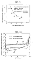
- (4) Fourth embodiment
A fourth embodiment of the present invention
will be described with reference to FIG. 9 and FIG.
10.FIG. 9 is a graph illustrating states of a
change of a relative dielectric constant (k) of an
insulating film relative to a gas pressure (P) of a
film forming gas and a relationship of a dielectric
breakdown-resistance of the insulating film after
annealing with the gas pressure (P) and the relative
dielectric constant (k). FIG. 10 is a graph
illustrating a barrier property of the insulating
film for copper, for the insulating film which is
prepared under a film forming condition IV.First, the preparation conditions of the samples
S1 to S4 used for this investigation will be
described. The treatment conditions prior to the
film formation and the annealing conditions after
the film formation are the same as those of the
first embodiment. The film forming conditions are
as follows.
-
(Film forming condition IV)
-
- (i) condition of film forming gas
- HMDSO flow rate: 50 sccm
- N2O flow rate: 400 sccm
- gas pressure: parameters (0.5, 0.75, 1.0 and
1.5 Torr, each corresponding to the samples S1 to
S4)
- (ii) condition for plasma formation
- high frequency power (13.56 MHz) PRF: 250 W
- low frequency power (380 KHz) PLF: 0 W
- (iii) substrate heating temperature: 375 °C
- (iv) formed silicon-containing insulating film
- film thickness: 100 nm
- relative dielectric constant: see FIG. 9
-
-
Measurement of the relative dielectric constant
was conducted before annealing in the same manner as
the first embodiment. Measurement of the dielectric
breakdown-resistance was conducted in the same
manner as that of the measurement method of the
leakage current of the first embodiment.
Examination of the barrier property of the formed
insulating film for copper was conducted by SIMS
(Secondary Ion Mass Spectroscopy).
-
FIG. 9 is the graph illustrating states of the
change of the relative dielectric constant (k) of
the insulating film relative to the gas pressure (P)
of the film forming gas and the relationship of the
dielectric breakdown-resistance of the insulating
film after annealing with the gas pressure (P) and
the relative dielectric constant (k).
-
In FIG. 9, the ordinate indicates the relative
dielectric constant (k) expressed by a linear scale,
and the abscissa indicates the gas pressure (P)
(Torr) of the film forming gas, which is expressed
by a linear scale. Moreover, the measurement points
are expressed by the symbol ○. In this case, the
symbol in the symbol ○ indicates that all of the
five measurement samples are not broken during the
dielectric breakdown-resistance test after annealing.
The symbol X in the symbol ○ indicates that all of
the five measurement samples are broken. Moreover,
the symbol Δ indicates that one or two measurement
samples among the five measurement samples are
broken. A sample in which current flows through the
insulating film from the early stage of voltage
application to the insulating film was judged to be
broken, and a sample, in which though the dielectric
breakdown voltage decreased after annealing, the
insulating film showed the breakdown voltage to some
degree, was judged to be sound. This is applied
also for fifth to tenth embodiments to be described
below.
-
According to the results shown in FIG. 9, as the
gas pressure (P) increases, the relative dielectric
constant (k) decreases. When the gas pressure (P)
is equal to 1.0 Torr or less, the insulating film
showed the dielectric breakdown-resistance, and did
not show the dielectric breakdown-resistance when
the gas pressure (P) was 1.5 Torr.
-
FIG. 10 is a graph illustrating investigation
results of the barrier property of the formed
insulating film for copper. The investigating
results of FIG. 10 are obtained by investigating the
copper distribution in the insulating film before
and after annealing by use of SIMS.
-
In FIG. 10, the ordinate indicates a copper
concentration (arbitrary unit) in the insulating
film, which is expressed by a logarithmic scale, and
the abscissa indicates measurement spots (nm)
measured from the surface of the insulating film,
which are expressed by a linear scale.
-
According to the results shown in FIG. 10, any
of the samples S1 to S4 contains copper in its
insulating film from the time when the samples S1 to
S4 are subjected to annealing, and this is
considered as that the insulating film is
adulterated with the copper during the film
formation. Accordingly, it is inevitable that the
change of the content of the copper in the
insulating film before and after annealing is
observed based on FIG. 10.
-
When the observation is made from this viewpoint,
as to the samples S3, none of the samples S3 was not
broken in the dielectric breakdown-resistance test,
but the samples S3 showed the copper diffusion into
the insulating film. On the other hand, in the
samples S1 and S2, the copper diffusion was hardly
observed even after annealing. Specifically, this
implies that the samples S1 and S2 possess the
barrier property.
- (5) Fifth embodiment
A fifth embodiment of the present invention will
be described with reference to FIG. 11.FIG. 11 is a graph illustrating states of a
change of a relative dielectric constant (k) of an
insulating film relative to a N2O gas flow rate in a
film forming gas and a relationship of a dielectric
breakdown-resistance of the insulating film after
annealing with the N2O gas flow rate and the
relative dielectric constant (k).First, preparation conditions of the samples S5
to S9 used in this investigation will be described.
Treatment conditions prior to the film formation and
annealing conditions are the same as those of the
first embodiment. The film forming conditions are
as follows.
-
(Film forming condition V)
-
- (i) condition of film forming gas
- HMDSO flow rate: 50 sccm
- N2O flow rate: parameters (100, 200, 400, 600
and 800 sccm, each corresponding to the samples S5
to S9)
- He flow rate: 400 sccm
- gas pressure (P): 1 Torr
- (ii) condition for plasma formation
- high frequency power (13.56 MHz) PRF: 250 W
- low frequency power (380 KHz) PLF: 0 W
- (iii) substrate heating temperature: 375 °C
- (iv) formed silicon-containing insulating film
- film thickness: 100 nm
- relative dielectric constant: see FIG. 11
Measurement of the relative dielectric constant
was conducted before annealing in the same manner as
the first embodiment. Measurement of the dielectric
breakdown-resistance was conducted in the same
manner as that of the measurement method of the
leakage current of the first embodiment.FIG. 11 is the graph illustrating states of the
change of the relative dielectric constant (k) of
the insulating film relative to the N2O gas flow
rate (sccm) in the film forming gas and the
relationship of the dielectric breakdown-resistance
of the insulating film after annealing with the N2O
gas flow rate and the relative dielectric constant
(k). In FIG. 11, the ordinate indicates a relative
dielectric constant (k) expressed by a linear scale,
and the abscissa indicates a N2O gas flow rate
(sccm) in the film forming gas expressed by a linear
scale.According to the results shown in FIG. 11, as
the N2O gas flow rate increases, the relative
dielectric constant (k) decreases. When the N2O gas
flow rate becomes higher than about 400 sccm, the
relative dielectric constant (k) increases as the
N2O gas flow rate becomes higher. The insulating
film showed the dielectric breakdown-resistance when
the N2O gas flow rate is equal to 400 sccm or less,
and did not show the dielectric breakdown-resistance
when the N2O gas flow rate was 600 sccm.
- (6) Sixth embodiment
-
-
A sixth embodiment of the present invention will
be described with reference to FIG. 12.
-
FIG 12 is a graph illustrating states of a
change of a relative dielectric constant (k) of an
insulating film relative to a He gas flow rate in a
film forming gas, and a relationship of a dielectric
breakdown-resistance of the insulating film after
annealing with the He gas flow rate and the relative
dielectric constant (k).
-
First, the preparation conditions of the samples
S10 to S14 used for this investigation will be
described. The treatment conditions prior to the
film formation and the annealing conditions are the
same as those of the first embodiment. The film
forming conditions are as follows.
(Film forming condition VI)
-
- (i) condition of film forming gas
- HMDSO flow rate: 50 sccm
- N2O flow rate: 400 sccm
- He flow rate: parameters (100, 200, 400, 600
and 800 sccm, each corresponding to the samples S10
to S14)
- gas pressure (P): 1 Torr
- (ii) condition for plasma formation
- high frequency power (13.56 MHz) PRF: 250 W
- low frequency power (380 KHz) PLF: 0 W
- (iii) substrate heating temperature: 375 °C
- (iv) formed silicon-containing insulating film
- film thickness: 100 nm
- relative dielectric constant: see FIG. 12
Measurement of the relative dielectric constant
was conducted before annealing in the same manner as
the first embodiment. Measurement of the dielectric
breakdown-resistance was conducted in the same
manner as that of the measurement method of the
leakage current of the first embodiment.FIG 12 is the graph illustrating the states of
the change of the relative dielectric constant (k)
of the insulating film relative to the He gas flow
rate in the film forming gas, and the relationship
of the dielectric breakdown-resistance of the
insulating film after annealing with the He gas flow
rate and the relative dielectric constant (k).In FIG. 12, the ordinate indicates the relative
dielectric constant (k) expressed by a linear scale,
and the abscissa indicates the He gas flow rate
(sccm) in the film forming gas, which is expressed
by a linear scale.According to the results shown in FIG. 12, as
the He gas flow rate became higher, the relative
dielectric constant (k) gradually increased. When
the He gas flow rate was equal to 400 sccm or less,
the insulating film did not show the dielectric
breakdown-resistance, and came to show the
dielectric breakdown-resistance when the He gas flow
rate exceeded 400 sccm.
- (7) Seventh embodiment
-
-
A seventh embodiment of the present invention
will be described with reference to FIG. 13.
-
FIG. 13 is a graph illustrating states of a
change of a relative dielectric constant (k) of an
insulating film relative to a N2O gas flow rate in a
film forming gas and a relationship of a dielectric
breakdown-resistance of the insulating film after
annealing with the N2O gas flow rate and the
relative dielectric constant (k). The seventh
embodiment differs from the fifth embodiment
(FIG.11) in that the film forming gas contains a NH3
gas.
-
First, the preparation conditions of the samples
S15 to S19 used for this investigation will be
described. The treatment conditions prior to the
film formation and the annealing conditions are the
same as those of the first embodiment. The film
forming conditions are as follows.
(Film forming condition VII)
-
- (i) condition of film forming gas
- HMDSO flow rate: 50 sccm
- N2O flow rate: parameters (100, 200, 400, 600
and 800 sccm, each corresponding to the samples S15
to S19)
- NH3 flow rate: 100 sccm
- He flow rate: 400 sccm
- gas pressure (P): 1 Torr
- (ii) condition for plasma formation
- high frequency power (13.56 MHz) PRF: 250 W
- low frequency power (380 KHz) PLF: 0 W
- (iii) substrate heating temperature: 375 °C
- (iv) formed silicon-containing insulating film
- film thickness: 100 nm
- relative dielectric constant: see FIG. 13
Measurement of the relative dielectric constant
was conducted in the same manner as the first
embodiment before annealing. Measurement of the
dielectric breakdown-resistance was conducted in the
same manner as that of the measurement method of the
leakage current of the first embodiment.FIG. 13 is the graph illustrating the states of
the change of the relative dielectric constant (k)
of the insulating film relative to the N2O gas flow
rate in the film forming gas and the relationship of
the dielectric breakdown-resistance of the
insulating film after annealing with the N2O gas
flow rate and the relative dielectric constant (k).In FIG. 13, the ordinate indicates the relative
dielectric constant (k) expressed by a linear scale,
and the abscissa indicates the N2O gas flow rate
(sccm) in the film forming gas, which is expressed
by a linear scale.According to the results shown in FIG. 13, as
the N2O gas flow rate becomes higher, the relative
dielectric constant (k) decreases. When the N2O gas
flow rate was at a range of 400 to 600 sccm, the
relative dielectric constant gradually increases.
All of the samples S15 to S19 show the dielectric
breakdown-resistance.
- (8) Eighth embodiment
-
-
An eighth embodiment of the present invention
will be described with reference to FIG. 14.
-
FIG. 14 is a graph illustrating states of a
change of a relative dielectric constant (k) of an
insulating film relative to a NH3 gas flow rate in a
film forming gas and a relationship of a dielectric
breakdown-resistance of the insulating film after
annealing with the NH3 gas flow rate and the
relative dielectric constant (k).
-
First, the preparation conditions of the samples
S20 to S24 used for this investigation will be
described. The treatment conditions prior to the
film formation and the annealing conditions are the
same as those of the first embodiment. The film
forming conditions are as follows.
(Film forming condition VIII)
-
- (i) condition of film forming gas
- HMDSO flow rate: 50 sccm
- N2O flow rate: 400 sccm
- NH3 flow rate: parameters (50, 100, 200, 400
and 600 sccm, each corresponding to the samples S20
to S24)
- gas pressure (P): 1 Torr
- (ii) condition for plasma formation
- high frequency power (13.56 MHz) PRF: 250 W
- low frequency power (380 KHz) PLF: 0 W
- (iii) substrate heating temperature: 375 °C
- (iv) formed silicon-containing insulating film
- film thickness: 100 nm
- relative dielectric constant: see FIG. 14
Measurement of the relative dielectric constant
was conducted in the same manner as the first
embodiment before annealing. Measurement of the
dielectric breakdown-resistance was conducted in the
same manner as that of the measurement method of the
leakage current of the first embodiment.FIG. 14 is a the graph illustrating the states
of the change of the relative dielectric constant
(k) of the insulating film relative to a NH3 gas
flow rate in the film forming gas and the
relationship of the dielectric breakdown-resistance
of the insulating film after annealing with the NH3
gas flow rate and the relative dielectric constant
(k).In FIG. 14, the ordinate indicates the relative
dielectric constant (k) expressed by a linear scale,
and the abscissa indicates the NH3 gas flow rate
(sccm) in the film forming gas, which is expressed
by a linear scale.According to the results shown in FIG. 14, when
the NH3 gas flow rate was 50 sccm, the relative
dielectric constant was about 3. Then, as the NH3
gas flow rate increased, the relative dielectric
constant (k) rapidly increased, and the relative
dielectric constant (k) stabilized at an almost
certain value (about 5) in case of 400 sccm or more
of the NH3 gas flow rate. All of the samples S20 to
S24 showed the dielectric breakdown-resistance.
- (9) Ninth embodiment
-
-
Based on the foregoing fourth to eighth
embodiments, it was proved that the dielectric
breakdown-resistance is larger as the relative
dielectric constant is higher. Therefore, it is
difficult for the single layers composed of the
insulating films according to the fourth to eighth
embodiments to meet the demand for a low relative
dielectric constant and a high dielectric breakdown-resistance.
In order to meet this demand, it is
suitable that the insulating film is at least
composed of two or more layers, in which an
insulating film showing an excellent dielectric
breakdown-resistance in spite of a high relative
dielectric constant and an insulating film showing a
low relative dielectric breakdown-resistance in
spite of a low relative dielectric constant are
stacked. In this case, particularly in order to
satisfactory meet a demand for the low relative
dielectric constant and the high dielectric
breakdown-resistance, it is preferable that an
insulating film showing an excellent dielectric
breakdown-resistance is made to be thin and an
insulating film showing a low relative dielectric
constant is made to be thick.
-
The experiment results of the ninth embodiment
of the present invention conducted in complying with
this spirit will be described with reference to FIGs.
15 to 18.
-
The ninth embodiment differs from the fourth to
eighth embodiments in that an insulating film
composed of a underlying film (symbol □) covering
copper and a main insulating film (symbol ○) formed
on the underlying film is formed. The thickness of
the underlying film was set to 10 nm, and the
thickness of the main insulating film was set to 90
nm. In this embodiment, the dielectric breakdown-resistance
of the entire two-layered structure
formed of the two insulating films was investigated.
-
In FIG. 15, the sorts (L1 to L3) of the
underlying films prepared by changing the gas
pressure P are shown, and the relationship between
the gas pressure P and the relative dielectric
constant is shown.
-
In FIG. 16, the sorts (L4 and L5) of the
underlying films prepared by changing the N2O gas
flow rate are shown, and the relationship between
the N2O gas flow rate and the relative dielectric
constant is shown.
-
In FIG. 17, the sorts (U1 to U3) of the main
insulating films prepared by changing the gas
pressure P are shown, and the relationship between
the gas pressure P and the relative dielectric
constant is shown.
-
In FIG. 18, the results obtained by
investigating the dielectric breakdown-resistance of
the two-layered insulating film (S25 to S31) in
which the underlying film of FIGs. 15 and 16 and the
main insulating film of FIG. 17 are combined.
-
FIG. 15 is a graph illustrating states of a
change of the relative dielectric constant (k) of a
underlying film relative to the gas pressure (P) of
a film forming gas. In FIG. 15, the ordinate
indicates the relative dielectric constant (k)
expressed by a linear scale, and the abscissa
indicates the gas pressure (P) (Torr) of the film
forming gas, which is expressed by a linear scale.
-
First, the preparation conditions of the samples
L1 to L3 used for this investigation will be
described. The treatment conditions prior to the
film formation and the annealing conditions are the
same as those of the first embodiment. The film
forming conditions are as follows.
(Film forming condition IX)
-
- (i) condition of film forming gas
- HMDSO flow rate: 50 sccm
- N2O flow rate: 400 sccm
- He gas flow rate: 400 sccm
- gas pressure (P): 0.5, 1.0 and 1.5 Torr (0.5
Torr for L1, 1.0 Torr for L2, and 1.5 Torr for L3)
- (ii) condition for plasma formation
- high frequency power (13.56 MHz) PRF: 250 W
- low frequency power (380 KHz) PLF: 0 W
- (iii) substrate heating temperature: 375 °C
- (iv) formed silicon-containing insulating film
(underlying film)
- film thickness: 10 nm
- relative dielectric constant: see FIG. 15
Measurements of the relative dielectric constant
were conducted before annealing in the same manner
as that of the first embodiment.According to the results shown in FIG. 15, as
the gas pressure (P) increases, the relative
dielectric constant (k) also increases. When the
gas pressure (P) is equal to 0.5 Torr, the relative
dielectric constant is about 3.5, and when the gas
pressure (P) is 1.0 Torr, the relative dielectric
constant is about 2.9, When the gas pressure P is
1.5 Torr, the relative dielectric constant is about
2.7.FIG. 16 is a graph illustrating states of a
change of the relative dielectric constant (k) of
the formed underlying film relative to the N2O gas
flow rate in the film forming gas. In FIG. 16, the
ordinate indicates the relative dielectric constant
(k) expressed by a linear scale, and the abscissa
indicates the N2O gas flow rate (sccm) in the film
forming gas, which is expressed by a linear scale.First, the preparation conditions of the samples
L4 and L5 used for this investigation will be
described. The treatment conditions prior to the
film formation and the annealing conditions are the
same as those of the first embodiment. The film
forming conditions are as follows.
-
(Film forming condition X)
-
- (i) condition of film forming gas
- HMDSO flow rate: 50 sccm
- N2O flow rate: 100 and 400 sccm (100 sccm for
L4, and 400 sccm for L5)
- He gas flow rate: 400 sccm
- gas pressure (P): 1.0 Torr
- (ii) condition for plasma formation
- high frequency power (13.56 MHz) PRF: 250 W
- low frequency power (380 KHz) PLF: 0 W
- (iii) substrate heating temperature: 375 °C
- (iv) formed silicon-containing insulating film
(underlying film)
- film thickness: 10 nm
- relative dielectric constant: see FIG. 16
Measurement of the relative dielectric constant
was conducted in the same manner as the first
embodiment before annealing.According to the results shown in FIG. 16, when
the N2O gas flow rate was 100 sccm, the relative
dielectric constant was about 3.1, and when the N2O
gas flow rate was 400 sccm, the relative dielectric
constant was about 2.9.FIG. 17 is a graph illustrating states of a
change of a relative dielectric constant (k) of a
main insulating film relative to a gas pressure P of
the film forming gas, which is prepared under a film
forming condition XI. In FIG. 17, the ordinate
indicates the relative dielectric constant (k)
expressed by a linear scale, and the abscissa
indicates the gas pressure (Torr) of the film
forming gas, which is expressed by a linear scale.First, the preparation conditions of the samples
U1 to U3 used for this investigation will be
described. The treatment conditions prior to the
film formation and the annealing conditions are the
same as those of the first embodiment. The film
forming conditions are as follows.
-
(Film forming condition XI)
-
- (i) condition of film forming gas
- HMDSO flow rate: 50 sccm
- N2O flow rate: 400 sccm
- He flow rate: 400 sccm
- gas pressure (P): 0.5, 1.0 and 1.5 Torr (0.5
Torr for U1, 1.0 Torr for U2, and 1.5 Torr is for
U3)
- (ii) condition for plasma formation
- high frequency power (13.56 MHz) PRF: 250 W
- low frequency power (380 KHz) PLF: 0 W
- (iii) substrate heating temperature: 375 °C
- (iv) formed silicon-containing insulating film
(main insulating film)
- film thickness: 90 nm
- relative dielectric constant: see FIG. 17
Measurements of the relative dielectric constant
were conducted before annealing in the same manner
as that of the first embodiment.According to the results shown in FIG. 17, as to
the main insulating film, when the gas pressure was
0.7 Torr, the relative dielectric constant was about
3.1, and when the gas pressure was 1.0 Torr, the
relative dielectric constant was about 2.9. When
the gas pressure was 1.5 Torr, the relative
dielectric constant was about 2.7.Next, concerning the two-layered insulating film
(S25 to S31) in which the main insulating film (U1
to U3) and the various underlying films (L1 to L5)
are combined, the dielectric breakdown-resistance
acquired will be described. The insulating film S25
is obtained by combining the underlying film L1 and
the main insulating film U1. The insulating film
S26 is obtained by combining the underlying film L1
and the main insulating film U2. The insulating
film S27 is obtained by combining the underlying
film L1 and the main insulating film U3. The
insulating film S28 is obtained by combining the
underlying film L2 and the main insulating film U3.
The insulating film S29 is obtained by combining the
underlying film L3 and the main insulating film U2.
The insulating film S30 is obtained by combining the
underlying film L4 and the main insulating film U3.
The insulating film S31 is obtained by combining the
underlying film L5 and the main insulating film U3.FIG. 18 is a graph illustrating a dielectric
breakdown-resistance acquired for the samples S25 to
S31. The abscissa indicates the relative dielectric
constant of the underlying film, which is expressed
by a linear scale, and the ordinate indicates the
relative dielectric constant of the main insulating
film, which is expressed by a linear scale.
Measurements of the dielectric breakdown-resistance
were conducted according to the same method as the
measurement method of the leakage current of the
first embodiment.According to FIG. 18, only the sample S29 has
insufficient dielectric breakdown-resistance, and
the samples other than the sample S29 have
sufficient dielectric breakdown-resistance. Herein,
with respect to the relative dielectric constant of
the underlying films, only the sample S29 has a
relative dielectric constant as low as 2.7, and the
samples other than the sample S29 have relative
dielectric constants of 2.9 or more. Moreover, with
respect to the relative dielectric constant of the
main insulating films, the samples S27, S28, S30 and
S31 have a relative dielectric constant as low as
2.7, and other samples have relative dielectric
constants of 2.9 or more. In other words, when the
relative dielectric constant of the underlying film
is low, the dielectric breakdown-resistance tends to
decrease irrespective of the magnitude of the
relative dielectric constant of the main insulating
film. Specifically, this implies that the
dielectric breakdown-resistance is decided depending
on the nature of the underlying film. In order to
increase the dielectric breakdown-resistance of the
two-layered insulating film, the relative dielectric
constant of the underlying film must be made to be
high to some degree.Based on these results, in order to meet the
demand for the low relative dielectric constant and
the high dielectric breakdown-resistance, the
insulating film is preferably formed so that the
underlying film is formed to be as thin as possible
by increasing the relative dielectric constant of
the underlying film to some degree, and so that the
insulating film has a thickness necessary to serve
as an interlayer insulating film by decreasing the
relative dielectric constant of the main insulating
film as low as possible.Although the invention has been described in
detail with reference to embodiments, the scope and
spirit of the present invention are not limited to
the specific examples described in the above-described
embodiments. It should be understood that
various changes, substitutions and alternations can
be made hereto without the parting from the spirit
and scope of the invention.For example, in the first embodiment, though
hexamethyldisiloxane (HMDSO) is used as the alkyl
compound having the siloxane bond, alkyl compounds
having the siloxane bond other than the foregoing
alkyl compound, for example, octamethylcyclotetrasiloxane
(OMCTS), tetramethylcyclotetrasiloxane
(TMCTS) or octamethyl-trisiloxane
(OMTS), can be used.Moreover, in the first embodiment, though the
dinitrogen monoxide (N2O) gas is used as the oxygen-containing
gas, any one of oxygen (O2), water (H2O)
and carbon dioxide (CO2) may be used instead of
dinitrogen monoxide (N2O).In the first to third embodiments, though the
gas containing hydrocarbon is not used, methane
(CH4) or acetylene (C2H2) may be added thereto.Furthermore, without using the alkyl compound
having the siloxane bond of the foregoing embodiment,
methyl silane or an alkyl compound having an O-Si-O
bond can alternatively be used.In this case, any one of monomethyl silane
(SiH3(CH3)), dimethyl silane (SiH2(CH3)2), trimethyl
silane (SiH(CH3)3) and tetramethyl silane (Si(CH3)4)
can be used as methyl silane. As the alkyl compound
having an O-Si-O bond, a compound having a
structural formula of CH3-O-Si(CH3)2-O-CH3 can be
used.As described above, according to the present
invention, a film forming gas containing an alkyl
compound and an oxygen-containing gas is supplied
between the first and second electrodes, and the gas
pressure is regulated to 1 Torr or less. Thereafter,
the high frequency power of a frequency of 1 MHz or
more is supplied to any one of the first and second
electrodes, and thus the film forming gas is
converted into a plasma state. The alkyl compound
and the oxygen-containing gas contained in the
plasmanized film forming gas are reacted with each
other, and the barrier insulating film covering the
copper wiring is formed.By use of the film forming gas converted into a
plasma state only by the high frequency power, it is
possible to achieve the low relative dielectric
constant. Moreover, by regulating the pressure of
the film forming gas to 1 Torr or less at least at
the early stage of the film formation, it is
possible to maintain the denseness of the insulating
film enough to prevent the copper diffusion.Moreover, by any one of the following methods or
combinations of them, denseness of the insulating
film can be enhanced while maintaining the low
relative dielectric constant: the insulating film is
formed while increasing the pressure of the film
forming gas from a low pressure to a pressure of 1
Torr gradually; the film forming gas containing at
least any one of ammonium (NH3) and nitrogen (N2) is
used for the formation of the insulating film; at
least any one of ammonium (NH3) and nitrogen (N2) is
added to the film forming gas at the early stage of
the film formation; the film forming gas containing
the dilution gas of at least any one of He and Ar is
used; the film forming gas containing the dilution
gas is used while increasing the flow rate of the
dilution gas; and the bias power of the low
frequency is applied at the early stage of the film
formation.Moreover, by adding the hydrocarbon, the formed
film can be enhanced in the etching selectivity for
the etchant of the insulating film with the low
relative dielectric constant.
-