EP1319260B1 - Coplanar waveguide switch - Google Patents
Coplanar waveguide switch Download PDFInfo
- Publication number
- EP1319260B1 EP1319260B1 EP01955268A EP01955268A EP1319260B1 EP 1319260 B1 EP1319260 B1 EP 1319260B1 EP 01955268 A EP01955268 A EP 01955268A EP 01955268 A EP01955268 A EP 01955268A EP 1319260 B1 EP1319260 B1 EP 1319260B1
- Authority
- EP
- European Patent Office
- Prior art keywords
- connection
- capacitor
- capacitance
- signal line
- waveguide
- Prior art date
- Legal status (The legal status is an assumption and is not a legal conclusion. Google has not performed a legal analysis and makes no representation as to the accuracy of the status listed.)
- Expired - Lifetime
Links
Images

Classifications
-
- H—ELECTRICITY
- H01—ELECTRIC ELEMENTS
- H01P—WAVEGUIDES; RESONATORS, LINES, OR OTHER DEVICES OF THE WAVEGUIDE TYPE
- H01P1/00—Auxiliary devices
- H01P1/10—Auxiliary devices for switching or interrupting
-
- H—ELECTRICITY
- H01—ELECTRIC ELEMENTS
- H01P—WAVEGUIDES; RESONATORS, LINES, OR OTHER DEVICES OF THE WAVEGUIDE TYPE
- H01P1/00—Auxiliary devices
- H01P1/10—Auxiliary devices for switching or interrupting
- H01P1/12—Auxiliary devices for switching or interrupting by mechanical chopper
- H01P1/127—Strip line switches
-
- H—ELECTRICITY
- H01—ELECTRIC ELEMENTS
- H01H—ELECTRIC SWITCHES; RELAYS; SELECTORS; EMERGENCY PROTECTIVE DEVICES
- H01H59/00—Electrostatic relays; Electro-adhesion relays
- H01H59/0009—Electrostatic relays; Electro-adhesion relays making use of micromechanics
Definitions
- Micromechanically fabricated high-frequency shorting switches consist of a thin metal bridge, which is stretched between the ground lines of a coplanar waveguide. Electrostatically, this bridge is pulled onto a thin dielectric, which is applied to the signal line, whereby the capacitance of the plate capacitor formed from bridge and signal line is increased. This capacitance between the signal line and ground line affects the propagation characteristics of the electromagnetic waves carried on the waveguide. In the “Off” booth (the metal bridge is below) much of the power is reflected. In the “on” state (the metal bridge is on top), much of the power is transmitted.
- a micromechanical switch is known, for example, from the document " Barker et al .: Distributed MEMS True-Time Delay 'Phase Shifters and Wide Band Switches', IEEE Transactions on Microwave Theory and Techniques, Vol. 46, No. 11, 1998, pages 1881-1889 , known. It is var forward to provide a plurality of parallel microbridges, each having a certain width and a certain distance from each other.
- microswitches are here by so-called cantilever, so clamped on one side. Microbar, trained.
- the device according to the invention with the features of the main claim has the advantage that the second connection is mechanically deformable so that the distance of the first connection and the second connection can be changed at least in a partial region of the second connection.
- a capacitor is produced by simple means whose capacity is variable.
- the length of the metal bridge ie the length of the second electrically conductive connection
- the distance of the ground lines of the coplanar waveguide can be chosen independently of the length of the second connection and vice versa.
- the first and second compounds are metallic compounds.
- all material-specific and process-technical advantages of the use of metals as electrically conductive compounds are used according to the invention.
- the capacitance change of the capacitor can be effected by an electrostatic force between the first connection and the second connection.
- the capacitor has a first predetermined capacitance and a second predetermined capacitance as a function of a predetermined electrical voltage between the first connection and the second connection.
- This makes it possible, by dimensioning in particular the first and second electrically conductive connection and the dielectric layer between the two, to determine the operating frequency within wide limits, independently of the distance of the ground lines of the coplanar waveguide.
- the insertion loss is adjustable thereby.
- the first connection forms an inductance in series with the capacitor between the signal line and the ground lines. This makes it possible to provide different shapes and dimensions for the first connection, so that the inductance resulting from the first connection can be predetermined within wide limits.
- the common impedance of the first capacitance and the inductance at an operating frequency substantially corresponds to its ohmic resistance. This makes it possible to achieve a particularly large insulation, ie a particularly large reflection coefficient, with switched off short circuit.
- the predetermined length is advantageously provided in such a way that reflections compensate at a transition between the signal line and the second connection. As a result, the insertion loss of the switch and thus the adjustment in the on state is improved.
- FIG. 1 shows a micromechanical high-frequency short circuit switch as an example of the device according to the invention with a capacitor.
- a coplanar waveguide is applied to a substrate 100.
- the coplanar waveguide consists in particular of three coplanar electrically conductive lines which, at least locally, are guided substantially parallel to one another.
- the lines of the coplanar waveguide are provided in particular metallic and applied to the substrate in particular by means of one or more galvanic process steps.
- the substrate 100 according to the invention has in particular the property of having a low loss angle.
- the two outer ones of the three lines of the coplanar waveguide correspond to a first ground line 110 and a second ground line 111, and the middle line corresponds to a signal line 120 of the coplanar waveguide.
- FIG. 1 is shown in plan view of interest for the inventive device section of such guided on the substrate 100 coplanar waveguide.
- the two ground lines 110, 111 of the coplanar waveguide are connected by means of a first electrically conductive connection 130.
- the first connection 130 is applied directly to the substrate 100 and has a small "height" in comparison to the "height" of the ground lines 110, 111, ie, the first connection 130 connects the ground lines 110, 111 to their "foot" the substrate 100.
- the signal line 120 of the coplanar waveguide is interrupted. Therefore, the connection 130 is also not electrically connected to the signal line 120.
- a layer of an in FIG. 1 Not applied dielectric applied.
- the interrupted signal line 120 is connected by means of a second electrically conductive connection 121.
- the second connection 121 is hereby provided according to the invention, in particular in the form of a metal connecting bridge between the ends of the interrupted signal line 120.
- the second connection 121 is provided at a certain distance from the plane of the substrate 100, wherein the distance between the second connection 121 to the substrate 100 and to the first connection 130 corresponds approximately to the height of the signal line 120.
- the second connection 121 In this respect, the second connection 121 "floats" between the ends of the interrupted signal line 120.
- the second connection 121 is also referred to as a bridge or metal bridge 121.
- a first, designated by the letter C cutting line, a designated by the letter A second cutting line and a letter marked with the third B section line are shown.
- the first cut line intersects the device according to the invention perpendicular to the course of the ground lines 110, 111 and the signal line 120 in the region of the first connection 130 between the ground lines 110, 111.
- the second section line intersects the device according to the invention parallel to the course of the lines 110, 111, 120 of coplanar waveguide in the region of the first ground line 110.
- the third section line cuts the device according to the invention parallel to the path of the lines 110, 111, 120 of the coplanar waveguide in the region of the signal line 120 or - where the signal line 120 is interrupted - in the region of the second connection 121st
- FIG. 2 is a sectional view of the device according to the invention along the first section line (letter C) from the FIG. 1 shown. It is the substrate again 100, the first ground line 110 and the second ground line 111 of the coplanar waveguide are shown. Between the ground lines 110, 111 of the coplanar waveguide, the signal line 120 of the waveguide is arranged.
- the spatial arrangement of the first connection 130 and the second connection 121 with respect to their distance from the surface of the substrate 100 is particularly clear.
- the first connection 130 is in FIG. 2 applied directly to the substrate 100, while the second connection 121 is applied to the signal line 120 and thus provided at a distance from the height of the signal or ground line 110, 111, 120 away from the plane of the substrate 100.
- FIG. 3 is the device according to the invention in a sectional view along the section line A from FIG. 1 shown. Only the substrate 100 and the first ground line 110 are visible.
- FIG. 4 the device according to the invention along the third section line (letter B) is shown.
- the signal line 120 of the coplanar waveguide is provided on the substrate 100.
- the signal line 120 is interrupted at a predetermined length 122.
- the second connection 121 bridges the signal line 120.
- the second connection 121 connects the two ends of the signal line 120 caused by the interruption of the signal line 120.
- the second connection 121 is provided in the exemplary embodiment, in particular at a distance from the substrate 100 the height of the signal line 120 corresponds.
- the first connection 130 is shown. Above the first connection 130 is already in connection with FIG. 1 addressed dielectric layer 140.
- FIG. 5 the device according to the invention is shown in perspective view.
- the substrate 100 On the substrate 100 is the first ground line 110 and the second ground line 111 of the waveguide. Between these ground lines 110, 111 is the interrupted signal line 120. The two ends of the signal line 120 are bridged by the second connection 121.
- the dielectric layer 140 is shown.
- the first connection 130 between the ground lines 110, 111 provided below the dielectric layer 140, ie in the direction of the substrate 100, is shown in FIG FIG. 5 not shown.
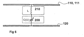
- FIG. 6 an equivalent circuit diagram of the arrangement according to the invention is shown.
- the two ground lines 110, 111 are shown only in the form of a single line of the coplanar waveguide. This is because the ground lines 110, 111 are at the same potential.
- the signal line 120 of the coplanar waveguide is in FIG. 6 shown.
- a capacitor 200 and an inductance 210 are arranged in series. The capacitor 200 is at least partially connected through the first connection 130 and the second connection 121, both in FIG FIG. 6 not shown realized.
- the capacitor 200 is provided variable in its capacity, and indeed according to the invention in particular the fact that the second connection 121 mechanically deformed and thus at least in some areas their distance to the first connection 130 changes, which affects the capacitance of the capacitor 200.
- the inductance 210 is essentially realized by the first connection 130.
- an inductance is generated, which can be predetermined by changing the length-width ratio, the shape, for example meandering or the like.
- the mechanically deformable second connection 121 is illustrated in the case in which the illustrated section of the coplanar waveguide has a high transmission coefficient and a low reflection coefficient.
- the distance between the first connection 130 and the second connection 121, which together with the electrical properties of the dielectric layer 140 decisively determine the capacitance of the capacitor 200, are in FIG FIG. 4 shown at maximum distance.
- the capacitance of the capacitor 200 is very small in this case and is decisive for the input attenuation of, for example, a short-circuit switch.
- an electrical voltage for example a DC voltage
- the second connection 121 since it is mechanically deformable, deformed and pulled into at least one subarea, namely essentially in the middle of the metal bridge, to the first connection 130 or to the dielectric layer 140 applied to the first connection 130.
- the dielectric in particular silicon dioxide or silicon nitride, prevents a galvanic contact of the device designed in particular as a switch in the off state.
- the capacitance of the capacitor 200 that is significantly formed from the first connection 130 and the second connection 121 changes, so that its capacitance becomes greater.
- the application or removal of an electrical voltage between the two connections 130, 121, the capacitance of the capacitor 200 of the device according to the invention changed and switched in the formation of the device as a switch.
- FIGS. 4 and 5 illustrated position of the second connection 121 corresponds to the operation of the device with passage and is switched as a switched-state.
- the in FIG. 4 not shown state of an attracted by an electrical voltage to the first connection 130 second connection 121 corresponds to an off switch. This is the case because it is provided according to the invention that the waveguide, which in the FIGS. 1 to 4 illustrated section is operated at a predetermined operating frequency.
- the capacitance of the capacitor 200 depending on an electrical voltage between the two connections 130, 121, assumes two capacitance values, which are referred to below as the first capacitance value or first capacitance and as the second capacitance value or second capacitance.
- the first capacitor corresponds to the switched-off state, ie, the first connection 121 is attracted to the first connection 130 due to the applied electrical voltage.
- the second capacity thus corresponds to the in FIG. 4 shown switched case where the second connection 121 is not mechanically deformed.
- the first capacitance and the second capacitance are determined by varying in particular the width and length of the first connection 130 and the second connection 121 as well as the thickness and the material properties of the dielectric layer and the height of the signal line 120.
- connections 130, 121, the dielectric layer 140 and the signal line 120 are dimensioned so that the impedance of a series connection of the first capacitor and an inductance formed by the first connection 130 in the Operating frequency is just canceled, or is as small as possible.
- the adjustment of the inductance 210 is done according to the invention essentially by the dimensioning and shaping of the first connection 130 between the ground lines 110, 111 of the waveguide.
- the second connection 121 is a thin metal bridge, which is stretched between the ends of the interrupted signal line 120 of the waveguide. Between the ground lines 110, 111, the first connection 130 acts as a DC short circuit.
- the first connection 130 acts with the second connection 121 as a plate capacitor.
- an inductance arranged in series with the plate capacitor can be set.
- a series resonant circuit is formed whose resonant frequency is in the off state of the second connection 121 by appropriate dimensioning of inductance and capacitance of the plate capacitor at the operating frequency of the device.
- the impedance between signal line 120 and the ground lines 110, 111 is greatly reduced compared to the impedance of the pure plate capacitor (without inductance), which significantly improves the isolation of a device designed as a high-frequency switch.
- the isolation is now limited by the ohmic losses in the second connection 121 and in the first connection 130.
- the device or the component or component at operating frequency by the reduced capacitance of the plate capacitor (second connection 121 or Bridge 121 " Up ", ie with a relatively large distance from the substrate) operated outside of this resonant frequency, so that no higher insertion loss results.
- the length of the second connection 121 is suitably dimensioned (eg half of the effective wavelength at the operating frequency)
- the reflections at the junctions or junctions between the coplanar waveguide (ie the ends of the signal line 120) and the second connection 121 compensate each other , whereby the insertion loss of the example provided as a switch Vorsch and thus the adaptation can be improved.
- the length of the second connection 121 is not limited by a maximum distance of the ground lines at high operating frequencies. As a result, at higher operating frequencies no increased switching voltage, ie between the first and the second connection 130 121 to be applied voltage to spend.
- the device according to the invention is particularly suitable for applications in the field of ACC (Adaptive Cruise Control) or SRR (Short Range Radar).
- ACC Adaptive Cruise Control
- SRR Short Range Radar
Description
Mikromechanisch gefertigte Hochfrequenz-Kurzschlußschalter bestehen aus einer dünnen Metallbrücke, welche zwischen die Masseleitungen eines koplanaren Wellenleiters gespannt ist. Elektrostatisch wird diese Brücke auf ein dünnes Dielektrikum, welches auf die Signalleitung aufgebracht ist, gezogen, wodurch die Kapazität des aus Brücke und Signalleitung gebildeten Plattenkondensators vergrößert wird. Diese Kapazität zwischen,Signalleitung und Masseleitung beeinflusst die Ausbreitungseigenschaften der auf dem Wellenleiter geführten elektromagnetischen Wellen. Im "Off"-Züstand (die Metallbrücke ist unten) wird ein Großteil der Leistung reflektiert. Im "On"-Zustand (die Metallbrücke ist oben) wird ein Großteil der Leistung transmittiert.Micromechanically fabricated high-frequency shorting switches consist of a thin metal bridge, which is stretched between the ground lines of a coplanar waveguide. Electrostatically, this bridge is pulled onto a thin dielectric, which is applied to the signal line, whereby the capacitance of the plate capacitor formed from bridge and signal line is increased. This capacitance between the signal line and ground line affects the propagation characteristics of the electromagnetic waves carried on the waveguide. In the "Off" booth (the metal bridge is below) much of the power is reflected. In the "on" state (the metal bridge is on top), much of the power is transmitted.
Ein mikromechanischer Schalter ist beispielsweise aus der Schrift "
In
Schließlich ist aus
Die erfindungsgemäße Vorrichtung mit den Merkmalen des Hauptanspruchs hat demgegenüber den Vorteil, dass die zweite Verbindung mechanisch so verformbar ist, dass der Abstand der ersten Verbindung und der zweiten Verbindung zumindest in einem Teilbereich der zweiten Verbindung änderbar ist. Dadurch wird mit einfachen Mittel ein Kondensator hergestellt, dessen Kapazität veränderbar ist.The device according to the invention with the features of the main claim has the advantage that the second connection is mechanically deformable so that the distance of the first connection and the second connection can be changed at least in a partial region of the second connection. As a result, a capacitor is produced by simple means whose capacity is variable.
Weiter ist von Vorteil, dass die Länge der Metallbrücke, d.h. die Länge der zweiten elektrisch leitenden Verbindung, nicht vom Abstand der Masseleitungen des koplanaren Wellenleiters abhängt, d.h. der Abstand der Masseleitungen des Wellenleiters kann unabhängig von der Länge der zweiten Verbindung und umgekehrt gewählt werden. Daraus ergibt sich der Vorteil, dass erfindungsgemäß ein HF-Mikroschalter mit den Merkmalen "geringer Abstand der Masseleitungen", "hohe Betriebsfrequenz", "große Ausdehnung der zweiten Verbindung, d.h. der Metallbrücke" und "geringe Schaltspannung" leicht realisierbar ist. Weiterhin ist es dadurch möglich, dass die durch die erste elektrisch leitende Verbindung zwischen den Masseleitungen des koplanaren Wellenleiters in Reihe zu dem Kondensator geschaltete Induktivität unabhängig von der Gestaltung der Signalleitung gewählt wird. Dadurch ist es mit einfachen Mitteln sowohl möglich, eine geringe Behinderung der Ausbreitung der elektromagnetischen Wellen entlang des Wellenleiters und eine optimale Dimensionierung der als Kurzschlußbrücke zwischen den Masseleitungen des Wellenleiters gestaltete erste Verbindung zu erreichen.It is furthermore advantageous that the length of the metal bridge, ie the length of the second electrically conductive connection, does not depend on the distance of the ground lines of the coplanar waveguide, ie the distance of the ground lines of the waveguide can be chosen independently of the length of the second connection and vice versa. This results in the advantage that, according to the invention, an HF microswitch with the features "short distance between the ground lines", "high operating frequency", "large extent of the second connection, ie the metal bridge" and "low switching voltage" can be easily realized. Furthermore, it is thereby possible that the inductance connected in series with the capacitor through the first electrically conductive connection between the ground lines of the coplanar waveguide is selected independently of the design of the signal line. That's it with simple means both possible to achieve a slight impediment to the propagation of the electromagnetic waves along the waveguide and optimum dimensioning of designed as a shorting bridge between the ground lines of the waveguide first connection.
Vorteilhafterweise sind die erste und die zweite Verbindung metallische Verbindungen. Dadurch finden sämtliche materialspezifische und prozeßtechnische Vorteile der Verwendung von Metallen als elektrisch leitende Verbindungen erfindungsgemäß Verwendung.Advantageously, the first and second compounds are metallic compounds. As a result, all material-specific and process-technical advantages of the use of metals as electrically conductive compounds are used according to the invention.
Vorteilhafterweise ist die Änderung der Kapazität des Kondensators durch eine elektrostatische Kraft zwischen der ersten Verbindung und der zweiten Verbindung bewirkbar. Dadurch sind mit einfachen Mitteln zwei Schaltzustände der erfindungsgemäßen Vorrichtung vorsehbar, so dass eine sichere und schnelle Schaltbarkeit der Vorrichtung gewährleistet ist. Darüber hinaus ist dadurch der Schaltzustand der Vorrichtung jederzeit eindeutig definiert.Advantageously, the capacitance change of the capacitor can be effected by an electrostatic force between the first connection and the second connection. As a result, with simple means two switching states the device according to the invention providable, so that a safe and fast switchability of the device is ensured. In addition, characterized the switching state of the device is always clearly defined.
Vorteilhafterweise weist der Kondensator in Abhängigkeit einer vorgegebenen elektrischen Spannung zwischen der ersten Verbindung und der zweiten Verbindung eine erste vorgegebene Kapazität und eine zweite vorgegebene Kapazität auf. Dadurch ist es möglich, durch Dimensionierung insbesondere der ersten und zweiten elektrisch leitenden Verbindung und der Dielektrizitätsschicht zwischen diesen beiden die Betriebsfrequenz in weiten Grenzen unabhängig von der Entfernung der Masseleitungen des koplanaren Wellenleiters zu bestimmen. Ebenso ist die Einfügedämpfung hierdurch einstellbar.Advantageously, the capacitor has a first predetermined capacitance and a second predetermined capacitance as a function of a predetermined electrical voltage between the first connection and the second connection. This makes it possible, by dimensioning in particular the first and second electrically conductive connection and the dielectric layer between the two, to determine the operating frequency within wide limits, independently of the distance of the ground lines of the coplanar waveguide. Likewise, the insertion loss is adjustable thereby.
Vorteilhafterweise bildet die erste Verbindung eine Induktivität in Reihe mit dem Kondensator zwischen der Signalleitung und den Masseleitungen. Hierdurch ist es möglich, für die erste Verbindung verschiedene Formen und Dimensionen vorzusehen,' so dass die durch die erste Verbindung resultierende Induktivität in weiten Grenzen vorgebbar ist.Advantageously, the first connection forms an inductance in series with the capacitor between the signal line and the ground lines. This makes it possible to provide different shapes and dimensions for the first connection, so that the inductance resulting from the first connection can be predetermined within wide limits.
Weiterhin entspricht vorteilhafterweise die gemeinsame Impedanz der ersten Kapazität und der Induktivität bei einer Betriebsfrequenz im Wesentlichen ihrem ohmschen Widerstand. Dadurch ist es möglich, eine besonders große Isolierung, d.h. einen besonders großen Reflexionskoeffizienten, bei ausgeschaltetem Kurzschlußschalter zu erreichen.Furthermore advantageously, the common impedance of the first capacitance and the inductance at an operating frequency substantially corresponds to its ohmic resistance. This makes it possible to achieve a particularly large insulation, ie a particularly large reflection coefficient, with switched off short circuit.
Weiterhin ist vorteilhafterweise als Betriebsfrequenz etwa 77 GHz oder etwa 24 GHz vorgesehen. Dadurch ist es möglich, die erfindungsgemäße Vorrichtung für ACC (Adaptive Cruise Control) oder SRR (Short Range Radar)-Anwendungen zu verwenden.Furthermore, it is advantageously provided as operating frequency about 77 GHz or about 24 GHz. This makes it possible to use the device according to the invention for ACC (Adaptive Cruise Control) or SRR (Short Range Radar) applications.
Weiterhin ist vorteilhafterweise die vorgegebene Länge derart vorgesehen, dass sich Reflexionen an einem Übergang zwischen der Signalleitung und der zweiten Verbindung kompensieren. Hierdurch wird die Einfügedämpfung des Schalters und somit die Anpassung im eingeschalteten Zustand verbessert.Furthermore, the predetermined length is advantageously provided in such a way that reflections compensate at a transition between the signal line and the second connection. As a result, the insertion loss of the switch and thus the adjustment in the on state is improved.
Ein Ausführungsbeispiel der Erfindung ist in der Zeichnung dargestellt und in der nachfolgenden Beschreibung näher erläutert. Es zeigen
-
Figur 1 eine erfindungsgemäße Vorrichtung mit einem Kondensator in Draufsicht, -
Figur 2 die erfindungsgemäße Vorrichtung mit einem Kondensator in Schnittdarstellung gemäß der Schnittlinie C ausFigur 1 , -
Figur 3 die erfindungsgemäße Vorrichtung mit einem Kondensator in Schnittdarstellung gemäß der Schnittlinie A ausFigur 1 , -
Figur 4 die erfindungsgemäße Vorrichtung mit einem Kondensator in Schnittdarstellung gemäß der Schnittlinie B ausFigur 1 , -
Figur 5 die erfindungsgemäße Vorrichtung mit Kondensator in einer perspektivischen Darstellung und -
Figur 6 ein Ersatzschaltbild der erfindungsgemäßen Vorrichtung mit Kondensator.
-
FIG. 1 a device according to the invention with a capacitor in plan view, -
FIG. 2 the device according to the invention with a capacitor in a sectional view according to the section line C fromFIG. 1 . -
FIG. 3 the device according to the invention with a capacitor in a sectional view according to the section line A fromFIG. 1 . -
FIG. 4 the device according to the invention with a capacitor in a sectional view according to the section line B fromFIG. 1 . -
FIG. 5 the inventive device with capacitor in a perspective view and -
FIG. 6 an equivalent circuit diagram of the device according to the invention with a capacitor.
In
In
In
In
In
In
Die zweite Verbindung 121 ist erfindungsgemäß eine dünne Metallbrücke, die zwischen die Enden der unterbrochenen Signalleitung 120 des Wellenleiters gespannt wird. Zwischen den Masseleitungen 110, 111 wirkt die erste Verbindung 130 als Gleichspannungskurzschluß. Die erste Verbindung 130 wirkt mit der zweiten Verbindung 121 als Plattenkondensator. Durch geeignete Dimensionierung und Formgebung des Gleichspannungskurzschlusses, d.h. der ersten Verbindung 130, kann eine zum Plattenkondensator in Reihe angeordnete Induktivität (bei Betriebsfrequenz) eingestellt werden. Durch die Induktivität in Reihe mit dem Plattenkondensator wird ein Serienschwingkreis gebildet, dessen Resonanzfrequenz im ausgeschalteten Zustand der zweiten Verbindung 121 durch geeignete Dimensionierung von Induktivität und Kapazität des Plattenkondensators bei der Betriebsfrequenz der Vorrichtung liegt. Dadurch wird die Impedanz zwischen Signalleitung 120 und den Masseleitungen 110, 111 gegenüber der Impedanz des reinen Plattenkondensators (ohne Induktivität) stark reduziert, wodoruch die Isolation einer als Hochfrequenz-Schalter ausgebildeten Vorrichtung wesentlich verbessert wird. Limitiert wird die Isolation nunmehr durch die ohmschen Verluste in der zweiten Verbindung 121 und in der ersten Verbindung 130. Im eingeschalteten Zustand wird die Vorrichtung bzw. das Bauteil oder Bauelement bei Betriebsfrequenz durch die verringerte Kapazität des Plattenkondensators (zweite Verbindung 121 oder auch Brücke 121 "oben", d.h. mit relativ großem Abstand zum Substrat) außerhalb dieser Resonanzfrequenz betrieben, so dass sich keine höhere Einfügedämpfung ergibt. Wird die Länge der zweiten Verbindung 121 geeignet dimensioniert (z. B. die Hälfte der effektiven Wellenlänge bei der Betriebsfrequenz) kompensieren sich die Reflexionen an den Stoßstellen bzw. den Übergangsstellen zwischen koplanarem Wellenleiter (d.h. den Enden der Signalleitung 120) und der zweiten Verbindung 121, wodurch die Einfügedämpfung der beispielsweise als Schalter vorgesehenen Vorrrichtung und somit die Anpassung verbessert werden. Dies entspricht einer Transformation der Impedanz der zweiten Verbindung 121 auf die Impedanz des koplanaren Wellenleiters. Die Länge der zweiten Verbindung 121 wird nicht durch einen Höchstabstand der Masseleitungen bei hohen Betriebsfrequenzen limitiert. Hierdurch ist bei höheren Betriebsfrequenzen keine vergrößerte Schaltspannung, d.h. zwischen die erste und die zweite Verbindung 130 121 anzulegende Spannung, aufzuwenden.The
Erfindungsgemäß ist insbesondere vorgesehen, die Betriebsfrequenz im Bereich von etwa 77 GHz oder etwa 24 GHz wählen zu können. Dadurch ist die erfindungsgemäße Vorrichtung insbesondere für Anwendungen im Bereich ACC (Adaptive Cruise Control) oder SRR (Short Range Radar) geeignet.According to the invention, it is provided in particular to be able to select the operating frequency in the range of about 77 GHz or about 24 GHz. As a result, the device according to the invention is particularly suitable for applications in the field of ACC (Adaptive Cruise Control) or SRR (Short Range Radar).
Claims (8)
- Apparatus having a capacitor (200) for varying the impedance of a sub-element of a coplanar waveguide, with the capacitance of the capacitor (200) being variable, with the capacitor (200) having a first electrically conductive connection (130) and a second electrically conductive connection (121) at least in places, with the signal line (120) of the sub-elements of the waveguide being interrupted over a predetermined length (122), with the first connection (130) connecting the earth lines (110, 111) of the waveguide, and with the second connection (121) connecting the two parts of the interrupted signal line (120), characterized in that, in order to vary the capacitance, the second connection (121) is in the form of a connection bridge over the first connection (130) and can be mechanically deformed such that the distance between the first connection (130) and the second connection (121) is variable, at least in a sub-area of the second connection (121).
- Apparatus according to Claim 1, characterized in that the first and the second connection (130, 121) are metallic connections.
- Apparatus according to one of the preceding claims, characterized in that the capacitance of the capacitor (200) can be varied by means of an electrostatic force between the first connection (130) and the second connection (121).
- Apparatus according to one of the preceding claims, characterized in that the capacitor (200) has a first predetermined capacitance and a second predetermined capacitance as a function of a predetermined electrical voltage between the first connection (130) and the second connection (121).
- Apparatus according to one of the preceding claims, characterized in that the first connection (130) forms an inductance (210) in series with the capacitor (200) between the signal line (120) and the earth lines (110, 111).
- Apparatus according to Claim 5, characterized in that the common impedance of the first capacitance and of the inductance (210) corresponds essentially to that resistance at an operating frequency.
- Apparatus according to Claim 6, characterized in that the operating frequency that is provided is about 77 GHz or about 24 GHz.
- Apparatus according to one of the preceding claims, characterized in that the predetermined length (122) is provided such that it compensates for reflections at a junction between the signal line (120) and the second connection (121).
Applications Claiming Priority (3)
| Application Number | Priority Date | Filing Date | Title |
|---|---|---|---|
| DE10037385A DE10037385A1 (en) | 2000-08-01 | 2000-08-01 | Device with a capacitor |
| DE10037385 | 2000-08-01 | ||
| PCT/DE2001/002757 WO2002011232A1 (en) | 2000-08-01 | 2001-07-20 | Coplanar waveguide switch |
Publications (2)
| Publication Number | Publication Date |
|---|---|
| EP1319260A1 EP1319260A1 (en) | 2003-06-18 |
| EP1319260B1 true EP1319260B1 (en) | 2008-08-20 |
Family
ID=7650904
Family Applications (1)
| Application Number | Title | Priority Date | Filing Date |
|---|---|---|---|
| EP01955268A Expired - Lifetime EP1319260B1 (en) | 2000-08-01 | 2001-07-20 | Coplanar waveguide switch |
Country Status (6)
| Country | Link |
|---|---|
| US (1) | US6686810B2 (en) |
| EP (1) | EP1319260B1 (en) |
| JP (1) | JP2004505578A (en) |
| KR (1) | KR20020035624A (en) |
| DE (2) | DE10037385A1 (en) |
| WO (1) | WO2002011232A1 (en) |
Families Citing this family (11)
| Publication number | Priority date | Publication date | Assignee | Title |
|---|---|---|---|---|
| DE10051311C1 (en) | 2000-10-17 | 2002-03-14 | Bosch Gmbh Robert | Capacitive device for impedance variation of coplanar waveguide has capacitance value adjusted by varying relative spacings between three conductive connections |
| DE10100296A1 (en) | 2001-01-04 | 2002-07-11 | Bosch Gmbh Robert | Device with a capacitor with variable capacitance, in particular high-frequency microswitches |
| DE10229038B4 (en) * | 2002-06-28 | 2013-08-14 | Robert Bosch Gmbh | Verkappes microstructure device with high-frequency feedthrough |
| DE10328183A1 (en) | 2002-07-02 | 2004-01-15 | Robert Bosch Gmbh | Electronic component comprises a base body having a passage connecting a first conducting structure with a second conducting structure both formed as planar waveguides |
| DE10342938A1 (en) * | 2003-09-17 | 2005-04-21 | Bosch Gmbh Robert | Component for impedance change in a coplanar waveguide and method for manufacturing a device |
| DE102006001321B3 (en) * | 2006-01-09 | 2007-07-26 | Protron Mikrotechnik Gmbh | Switching device, has two signal lines and ground lines which are controlled by plated-through hole through laminar extending substrate, where signal lines surrounded by ground lines |
| DE102007035633B4 (en) | 2007-07-28 | 2012-10-04 | Protron Mikrotechnik Gmbh | Process for producing micromechanical structures and micromechanical structure |
| CN103474734B (en) * | 2013-08-20 | 2016-08-10 | 京信通信技术(广州)有限公司 | Electric bridge |
| CA2852858A1 (en) * | 2014-05-30 | 2015-11-30 | C-Com Satellite Systems Inc. | Phase shifter |
| US11515609B2 (en) * | 2019-03-14 | 2022-11-29 | Taiwan Semiconductor Manufacturing Company, Ltd. | Transmission line structures for millimeter wave signals |
| DE102019126433A1 (en) | 2019-03-14 | 2020-09-17 | Taiwan Semiconductor Manufacturing Company, Ltd. | Transmission line structures for millimeter wave signals |
Citations (1)
| Publication number | Priority date | Publication date | Assignee | Title |
|---|---|---|---|---|
| US5619061A (en) * | 1993-07-27 | 1997-04-08 | Texas Instruments Incorporated | Micromechanical microwave switching |
Family Cites Families (4)
| Publication number | Priority date | Publication date | Assignee | Title |
|---|---|---|---|---|
| US5087896A (en) * | 1991-01-16 | 1992-02-11 | Hughes Aircraft Company | Flip-chip MMIC oscillator assembly with off-chip coplanar waveguide resonant inductor |
| US5528203A (en) * | 1994-09-26 | 1996-06-18 | Endgate Corporation | Coplanar waveguide-mounted flip chip |
| CA2211830C (en) * | 1997-08-22 | 2002-08-13 | Cindy Xing Qiu | Miniature electromagnetic microwave switches and switch arrays |
| KR100344790B1 (en) * | 1999-10-07 | 2002-07-19 | 엘지전자주식회사 | Super-high frequency tunable filter using micromechanical systems |
-
2000
- 2000-08-01 DE DE10037385A patent/DE10037385A1/en not_active Withdrawn
-
2001
- 2001-07-20 KR KR1020027004157A patent/KR20020035624A/en not_active Application Discontinuation
- 2001-07-20 WO PCT/DE2001/002757 patent/WO2002011232A1/en active IP Right Grant
- 2001-07-20 US US10/089,618 patent/US6686810B2/en not_active Expired - Fee Related
- 2001-07-20 EP EP01955268A patent/EP1319260B1/en not_active Expired - Lifetime
- 2001-07-20 JP JP2002516855A patent/JP2004505578A/en active Pending
- 2001-07-20 DE DE50114251T patent/DE50114251D1/en not_active Expired - Lifetime
Patent Citations (1)
| Publication number | Priority date | Publication date | Assignee | Title |
|---|---|---|---|---|
| US5619061A (en) * | 1993-07-27 | 1997-04-08 | Texas Instruments Incorporated | Micromechanical microwave switching |
Also Published As
| Publication number | Publication date |
|---|---|
| WO2002011232A1 (en) | 2002-02-07 |
| DE10037385A1 (en) | 2002-02-14 |
| US6686810B2 (en) | 2004-02-03 |
| DE50114251D1 (en) | 2008-10-02 |
| KR20020035624A (en) | 2002-05-11 |
| US20030030505A1 (en) | 2003-02-13 |
| JP2004505578A (en) | 2004-02-19 |
| EP1319260A1 (en) | 2003-06-18 |
Similar Documents
| Publication | Publication Date | Title |
|---|---|---|
| DE60308100T2 (en) | High frequency switch and electronic device using this | |
| DE60314875T2 (en) | MICROELECTROMECHANIC HF SWITCH | |
| DE60312665T2 (en) | Stop electrostatically activated microelectromechanical switching system | |
| EP1319260B1 (en) | Coplanar waveguide switch | |
| DE60115086T2 (en) | CONTACT STRUCTURE FOR MICRO RELAY FOR RF APPLICATIONS | |
| DE60007736T2 (en) | MICROMECHANICAL SWITCH AND CORRESPONDING MANUFACTURING METHOD | |
| DE60305349T2 (en) | TRANSITION FROM A RECTANGULAR HOLLOWER TO A MICRO-STRIP LINE | |
| DE60223479T2 (en) | Adapted broadband switching matrix with active diode isolation | |
| DE69930169T2 (en) | MICROMECHANICAL SWITCH | |
| EP1350281B1 (en) | Device comprising a capacitor having a varying capacitance, especially a high- frequency microswitch | |
| EP1719144B1 (en) | High-frequency mems switch comprising a curved switching element and method for producing said switch | |
| DE60307136T2 (en) | MICROMECHANICAL ELECTROSTATIC SWITCH WITH LOW OPERATING VOLTAGE | |
| DE10051311C1 (en) | Capacitive device for impedance variation of coplanar waveguide has capacitance value adjusted by varying relative spacings between three conductive connections | |
| EP1266422A1 (en) | Phase shifters and arrangement consisting of several phase shifters | |
| DE69837078T2 (en) | Low loss air bearing radial combined stripline for N-way RF switch | |
| EP1665315B1 (en) | Component for modifying the impedance of a coplanar waveguide and method for producing such a component | |
| DE60307672T2 (en) | MICROMECHANICAL ELECTROSTATIC SWITCH WITH LOW OPERATING VOLTAGE | |
| DE60314470T2 (en) | Network for bias supply for balanced lines | |
| WO2005064740A1 (en) | Stripline directional coupler having a wide coupling gap | |
| DE102004062992B4 (en) | Switchable high-frequency MEMS element with movable switching element and method for its production | |
| EP1495513A1 (en) | Electric matching network with a transformation line | |
| Muldavin et al. | Novel series and shunt MEMS switch geometries for X-band applications | |
| DE10238947A1 (en) | Coplanar phase shifter with constant damping | |
| DE102004064163B4 (en) | Switchable, high-frequency, micro-electromechanical system component, combines signal line and switching component in common plane on substrate | |
| WO2005038976A1 (en) | Electrical adaptation network comprising a transformation line |
Legal Events
| Date | Code | Title | Description |
|---|---|---|---|
| PUAI | Public reference made under article 153(3) epc to a published international application that has entered the european phase |
Free format text: ORIGINAL CODE: 0009012 |
|
| 17P | Request for examination filed |
Effective date: 20030303 |
|
| AK | Designated contracting states |
Designated state(s): AT BE CH CY DE DK ES FI FR GB GR IE IT LI LU MC NL PT SE TR |
|
| RBV | Designated contracting states (corrected) |
Designated state(s): AT BE CH DE FR GB IT LI |
|
| 17Q | First examination report despatched |
Effective date: 20070713 |
|
| GRAP | Despatch of communication of intention to grant a patent |
Free format text: ORIGINAL CODE: EPIDOSNIGR1 |
|
| RBV | Designated contracting states (corrected) |
Designated state(s): CH DE FR GB IT LI |
|
| GRAS | Grant fee paid |
Free format text: ORIGINAL CODE: EPIDOSNIGR3 |
|
| GRAA | (expected) grant |
Free format text: ORIGINAL CODE: 0009210 |
|
| AK | Designated contracting states |
Kind code of ref document: B1 Designated state(s): CH DE FR GB IT LI |
|
| REG | Reference to a national code |
Ref country code: GB Ref legal event code: FG4D Free format text: NOT ENGLISH |
|
| REG | Reference to a national code |
Ref country code: CH Ref legal event code: EP |
|
| REF | Corresponds to: |
Ref document number: 50114251 Country of ref document: DE Date of ref document: 20081002 Kind code of ref document: P |
|
| PLBE | No opposition filed within time limit |
Free format text: ORIGINAL CODE: 0009261 |
|
| STAA | Information on the status of an ep patent application or granted ep patent |
Free format text: STATUS: NO OPPOSITION FILED WITHIN TIME LIMIT |
|
| 26N | No opposition filed |
Effective date: 20090525 |
|
| PGFP | Annual fee paid to national office [announced via postgrant information from national office to epo] |
Ref country code: CH Payment date: 20100726 Year of fee payment: 10 |
|
| PGFP | Annual fee paid to national office [announced via postgrant information from national office to epo] |
Ref country code: GB Payment date: 20100726 Year of fee payment: 10 |
|
| REG | Reference to a national code |
Ref country code: CH Ref legal event code: PL |
|
| GBPC | Gb: european patent ceased through non-payment of renewal fee |
Effective date: 20110720 |
|
| PG25 | Lapsed in a contracting state [announced via postgrant information from national office to epo] |
Ref country code: CH Free format text: LAPSE BECAUSE OF NON-PAYMENT OF DUE FEES Effective date: 20110731 Ref country code: LI Free format text: LAPSE BECAUSE OF NON-PAYMENT OF DUE FEES Effective date: 20110731 |
|
| PG25 | Lapsed in a contracting state [announced via postgrant information from national office to epo] |
Ref country code: GB Free format text: LAPSE BECAUSE OF NON-PAYMENT OF DUE FEES Effective date: 20110720 |
|
| PGFP | Annual fee paid to national office [announced via postgrant information from national office to epo] |
Ref country code: FR Payment date: 20120803 Year of fee payment: 12 Ref country code: IT Payment date: 20120725 Year of fee payment: 12 |
|
| REG | Reference to a national code |
Ref country code: FR Ref legal event code: ST Effective date: 20140331 |
|
| PG25 | Lapsed in a contracting state [announced via postgrant information from national office to epo] |
Ref country code: IT Free format text: LAPSE BECAUSE OF NON-PAYMENT OF DUE FEES Effective date: 20130720 Ref country code: FR Free format text: LAPSE BECAUSE OF NON-PAYMENT OF DUE FEES Effective date: 20130731 |
|
| PGFP | Annual fee paid to national office [announced via postgrant information from national office to epo] |
Ref country code: DE Payment date: 20140925 Year of fee payment: 14 |
|
| REG | Reference to a national code |
Ref country code: DE Ref legal event code: R119 Ref document number: 50114251 Country of ref document: DE |
|
| PG25 | Lapsed in a contracting state [announced via postgrant information from national office to epo] |
Ref country code: DE Free format text: LAPSE BECAUSE OF NON-PAYMENT OF DUE FEES Effective date: 20160202 |