BACKGROUND OF THE INVENTION
-
The present invention relates to a method of fabricating
a semiconductor integrated circuit device and a method of
fabricating a multichip module, more particularly, to a
technique effectively applicable to a photolithography
(hereinafter, referred to as lithography) technique in which a
predetermined pattern is printed onto a semiconductor wafer
(hereinafter, referred to as wafer) with using a photomask
(hereinafter, referred to as mask) in the fabrication process
of a semiconductor integrated circuit device.
-
In the fabrication of a semiconductor integrated circuit
device (LSI: Large Scale Integrated Circuit), the lithography
technique is used as a method of forming a fine pattern on a
wafer. As the lithography technique, a so-called optical
projection exposure method, in which a pattern formed on each
mask is repeatedly printed onto a wafer through reduced
projection optics, has become the mainstream. The basic
constitution of the exposure tool is disclosed in Japanese
Patent Laid-open No. 2000-91192.
-
The resolution R on the wafer in this projection exposure
method is generally represented by: R = k × λ / NA, where k
represents a constant depending on a resist material and a
process, λ represents a wavelength of exposure light, and NA
represents numerical aperture of a projection lens. As is
apparent from the relational expression, as the pattern becomes
finer, a projection exposure technique using the light source
having shorter wavelength has become necessary. At the present,
the LSI is fabricated by a projection exposure tool using an i-ray
(λ = 365 nm) of a mercury lamp or a KrF excimer laser (λ =
248 nm) as an illumination light source. In order to make the
pattern further finer, a light source having a shorter
wavelength is required, and the employment of an ArF excimer
laser (λ = 193 nm) or an F2 laser (λ = 157 nm) has been examined.
-
Meanwhile, the above-mentioned mask used in the
projection exposure method has a structure in which an opaque
pattern made of, for example, chromium or the like is formed as
an opaque film on a quartz glass substrate transparent to an
exposure light. The fabrication method thereof is, for example,
as follows. That is, a chromium film serving as an opaque film
is first formed on a quartz glass substrate, and a resist film
reactive to an electron beam is coated thereon. Subsequently,
an electron beam is irradiated onto the resist film according
to pattern data predetermined, and then a resist pattern is
formed by performing the development thereto. Subsequently, the
chromium thin film is etched with using the resist pattern as
an etching mask to form an opaque pattern made of chromium or
the like. Lastly, the remaining resist film reactive to an
electron beam is removed, and thus, the fabrication of a mask
is completed.
SUMMARY OF THE INVENTION
-
However, the inventors of the present invention have
found out that the exposure technique using a mask having an
opaque pattern made of a metal film such as chromium or the
like has problems as follows.
-
Specifically, the mask having an opaque pattern made of a
metal film is advantageous in mass production because it has
good durability and high reliability and is capable of being
used in a large amount of exposure. However, when such a mask
is used in the development period of a semiconductor integrated
circuit device or in the fabrication of a small number of
various semiconductor integrated circuit devices, in other
words, in the case where changes and modifications are
frequently made in the mask pattern and the same mask is rarely
used in different processes, a great amount of time and
increased cost are required to fabricate the mask. Therefore,
there arise such problems as to hinder the improvement in
productivity of and the reduction in fabrication cost of a
semiconductor integrated circuit device.
-
An object of the present invention is to provide a
technique capable of improving the productivity of a
semiconductor integrated circuit device.
-
Also, another object of the present invention is to
provide a technique capable of reducing a development period
required to develop a semiconductor integrated circuit device.
-
Also, another object of the present invention is to
provide a technique capable of reducing a fabrication period
required to fabricate a semiconductor integrated circuit device.
-
Also, another object of the present invention is to
provide a technique capable of reducing the cost of a
semiconductor integrated circuit device.
-
The above and other objects and novel characteristics of
the present invention will be apparent from the description of
the present specification and the accompanying drawings.
-
The advantages achieved by the typical ones of the
inventions disclosed in the present application will be briefly
described as follows.
-
Specifically, in the present invention, a mask having a
metal film as an opaque member relative to an exposure light
and a mask having, as an opaque member, an organic material
containing an organic photoreactive resin film relative to an
exposure light are used in an exposure treatment of the
fabrication steps of a semiconductor integrated circuit device.
-
Also, in the present invention, a mask having a metal
film as an opaque member relative to an exposure light and a
mask having, as an opaque member, an organic material
containing an organic photoreactive resin film relative to an
exposure light are properly used, depending on how to use the
mask, in an exposure process of the fabrication steps of a
semiconductor integrated circuit device.
-
Also, in the present invention, the organic material is
made of a single film of the organic photoreactive resin film.
-
Also, in the present invention, the organic material is
made by adding a photo-absorbing material or a photo-attenuating
material to the organic photoreactive resin film.
-
Also, in the present invention, the organic material is
made of a laminated film of the organic photoreactive resin
film and the photo-absorbing film, a laminated film of the
organic photoreactive resin film and the photo-attenuating film,
or a laminated film of the organic photoreactive resin film and
an anti-reflective layer.
-
Also, in the present invention, the mask having an
organic material containing an organic photoreactive resin film
as an opaque member relative to an exposure light includes also
a pattern made of a metal film as an opaque member relative to
an exposure light.
-
Also, in the present invention, the mask having an
organic material containing the organic photoreactive resin
film as an opaque member relative to an exposure light includes
also a pattern made of a metal film as an opaque member
relative to an exposure light, and the pattern made of metal
film serving as the opaque member is a pattern functioning to
print an integrated circuit pattern onto a wafer.
-
Also, in the present invention, the mask having an
organic material containing organic photoreactive resin film as
an opaque member to an exposure light has also a pattern made
of a metal film as an opaque member to an exposure light, and
the pattern made of metal film serving as the opaque member is
a metal film covering a peripheral region of the mask.
-
Also, in the present invention, when fabricating the mask
having an organic material containing organic photoreactive
resin film as an opaque member to an exposure light, a step of
removing an opaque member made of the organic material, and
then forming a new opaque member made of the organic material
is performed.
-
Also, in the present invention, when fabricating the mask
having an organic material containing organic photoreactive
resin film as an opaque member to an exposure light, a step of
removing an opaque member made of the organic material, and
then forming a new opaque member made of the organic material
is performed, wherein the newly formed opaque member made of
the organic material serves as a pattern used to print an
integrated circuit pattern onto a wafer.
BRIEF DESCRIPTIONS OF THE DRAWINGS
-
- FIG. 1 is a flow chart showing the fabrication process of
a semiconductor integrated circuit device according to an
embodiment of the present invention.
- FIG. 2 is an explanatory diagram showing an example of an
exposure tool used in the fabrication process of the
semiconductor integrated circuit device in FIG. 1.
- FIG. 3A is a plan view showing an example of a photomask
used in the fabrication process of the semiconductor integrated
circuit device in FIG. 1.
- FIG. 3B is a cross-sectional view taken along line A-A in
FIG. 3A.
- FIG. 4A is a plan view showing an example of a photomask
used in the fabrication process of the semiconductor integrated
circuit device in FIG. 1
- FIG. 4B is a cross-sectional view taken along line A-A in
FIG. 4A.
- FIG. 5A is a plan view showing an example of a photomask
used in the fabrication process of the semiconductor integrated
circuit device in FIG. 1.
- FIG. 5B is a cross-sectional view taken along line A-A in
FIG. 5A.
- FIG. 6A is a plan view showing an example of a photomask
used in the fabrication process of the semiconductor integrated
circuit device in FIG. 1.
- FIG. 6B is a cross-sectional view taken along line A-A in
FIG. 6A.
- FIG. 7A is a plan view showing an example of a photomask
used in the fabrication process of the semiconductor integrated
circuit device in FIG. 1.
- FIG. 7B is a cross-sectional view taken along line A-A in
FIG. 7A.
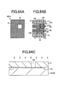
- FIG. 8A is a cross-sectional view during fabrication
process of a conventional photomask.
- FIG. 8B is a cross-sectional view during fabrication
process of a conventional photomask.
- FIG. 8C is a cross-sectional view during the fabrication
process of a conventional photomask.
- Fig. 8D is a cross-sectional view during the fabrication
process of a conventional photomask.
- FIG. 9A is a plan view showing an example of a photomask
used in the fabrication process of the semiconductor integrated
circuit device in FIG. 1.
- FIG. 9B is a cross-sectional view taken along line A-A in
FIG. 9A.
- FIG. 9C is an enlarged view showing the principal part of
FIG. 9B.
- FIG. 9D shows a modification example of an opaque member
and is an enlarged plan view showing the principal part of FIG.
9B.
- FIG. 10A is a plan view showing an example of the
photomask used in the fabrication process of the semiconductor
integrated circuit device in FIG. 1.
- FIG. 10B is a cross-sectional view taken along line A-A
in FIG. 10A.
- FIG. 11A is a plan view showing an example of the
photomask used in the fabrication process of the semiconductor
integrated circuit device in FIG. 1.
- FIG. 11B is a cross-sectional view taken along line A-A
in FIG. 11A.
- FIG. 12A is a plan view during the fabrication process of
the photomask shown in FIG. 9.
- FIG. 12B is a cross-sectional view taken along line A-A
in FIG. 12A.
- FIG. 13A is a plan view during the fabrication process of
the photomask shown in FIG. 9 subsequently to FIG. 12.
- FIG. 13B is a cross-sectional view taken along line A-A
in FIG. 13A.
- FIG. 14A is a plan view during the fabrication process of
the photomask shown in FIG. 9 subsequently to FIG. 13.
- FIG. 14B is a cross-sectional view taken along line A-A
in FIG. 14A.
- FIG. 15A is a plan view during the fabrication process of
the photomask shown in FIG. 9 subsequently to FIG. 14.
- FIG. 15B is a cross-sectional view taken along line A-A
in FIG. 15A.
- FIG. 16A is a plan view during the fabrication process of
the photomask shown in FIG. 9 subsequently to FIG. 15.
- FIG. 16B is a cross-sectional view taken along line A-A
in FIG. 16A.
- FIG. 17A is a plan view during a re-fabrication process
of the photomask shown in FIG. 9.
- FIG. 17B is a cross-sectional view taken along line A-A
in FIG. 17A.
- FIG. 18A is a plan view during the re-fabrication process
of the photomask shown in FIG. 9 subsequently to FIG. 17.
- FIG. 18B is a cross-sectional view taken along line A-A
in FIG. 18A.
- FIG. 19A is a plan view during the re-fabrication process
of the photomask shown in FIG. 9 subsequently to FIG. 18.
- FIG. 19B is a cross-sectional view taken along line A-A
in FIG. 19A.
- FIG. 20A is a plan view showing an example of a photomask
used in the fabrication process of the semiconductor integrated
circuit device in FIG. 1.
- FIG. 20B is a cross-sectional view taken along line A-A
in FIG. 20A.
- FIG. 21A is a plan view showing an example of a photomask
used in the fabrication process of the semiconductor integrated
circuit device in FIG. 1.
- FIG. 21B is a cross-sectional view taken along line A-A
in FIG. 21A.
- FIG. 22A is a plan view showing an example of a photomask
used in the fabrication process of the semiconductor integrated
circuit device in FIG. 1.
- FIG. 22B is a cross-sectional view taken along line A-A
in FIG. 22A.
- FIG. 23A is a plan view during the fabrication process of
the photomask shown in FIG. 20.
- FIG. 23B is a cross-sectional view taken along line A-A
in FIG. 23A.
- FIG. 24A is a plan view during the fabrication process of
the photomask shown in FIG. 20 subsequently to FIG. 23.
- FIG. 24B is a cross-sectional view taken along line A-A
in FIG. 24A.
- FIG. 25A is a plan view during the re-fabrication process
of the photomask shown in FIG. 20.
- FIG. 25B is a cross-sectional view taken along line A-A
in FIG. 25A.
- FIG. 26A is a plan view during the re-fabrication process
of the photomask shown in FIG. 25 subsequently to FIG. 25.
- FIG. 26B is a cross-sectional view taken along line A-A
in FIG. 26A.
- FIG. 27A is a plan view during the re-fabrication process
of the photomask shown in FIG. 25 subsequently to FIG. 26.
- FIG. 27B is a cross-sectional view taken along line A-A
in FIG. 27A.
- FIG. 28A is a plan view showing an example of the
photomask used in the fabrication process of the semiconductor
- integrated circuit device in FIG. 1.
- FIG. 28B is a cross-sectional view taken along line A-A
in FIG. 28A.
- FIG. 29A is a plan view showing an example of the
photomask used in the fabrication process of the semiconductor
integrated circuit device in FIG. 1.
- FIG. 29B is a cross-sectional view taken along line A-A
in FIG. 29A.
- FIG. 30A is a plan view showing an example of the
photomask used in the fabrication process of the semiconductor
integrated circuit device in FIG. 1.
- FIG. 30B is a cross-sectional view taken along line A-A
in FIG. 30A.
- FIG. 31A is a plan view showing the principal part of an
example of the photomask used in the fabrication process of the
semiconductor integrated circuit device of FIG. 1.
- FIG. 31B is a plan view showing the principal part of the
pattern printed by using the photomask shown in FIG. 31A.
- FIG. 31C is a plan view showing the principal part of the
photomask in FIG. 31A in a state where an opaque member made of
an organic material containing an organic photoreactive resin
film of the photomask is removed.
- FIG. 31D is a plan view showing the principal part of a
semiconductor wafer illustrating a pattern to be printed, by
the use of the photomask of FIG. 31C, onto a semiconductor
wafer.
- FIG. 32A is a plan view showing an example of the
photomask used in the fabrication process of the semiconductor
integrated circuit device in FIG. 1.
- FIG. 32B is a cross-sectional view taken along line A-A
in FIG. 32A.
- FIG. 33A is a plan view during the fabrication process of
the photomask shown in FIG. 28.
- FIG. 33B is a cross-sectional view taken along line A-A
in FIG. 33A.
- FIG. 34A is a plan view during the fabrication process of
the photomask shown in FIG. 28 subsequently to FIG. 33.
- FIG. 34B is a cross-sectional view taken along line A-A
in FIG. 34A.
- FIG. 35A is a plan view during the fabrication process of
the photomask shown in FIG. 29.
- FIG. 35B is a cross-sectional view taken along line A-A
in FIG. 35A.
- FIG. 36A is a plan view during the fabrication process of
the photomask shown in FIG. 30.
- FIG. 36B is a cross-sectional view taken along line A-A
in FIG. 36A.
- FIG. 37A is a plan view during the fabrication process of
the photomask subsequently to FIG. 34.
- FIG. 37B is a cross-sectional view taken along line A-A
in FIG. 37A.
- FIG. 38A is a plan view during the re-fabrication process
of the photomask shown in FIG. 28.
- FIG. 38B is a cross-sectional view taken along line A-A
in FIG. 38A.
- FIG. 39A is a plan view during the re-fabrication process
of the photomask shown in FIG. 28 subsequently to FIG. 38.
- FIG. 39B is a cross-sectional view taken along line A-A
in FIG. 39A.
- FIG. 40A is a plan view during the re-fabrication process
of the photomask shown in FIG. 28 subsequently to FIG. 39.
- FIG. 40B is a cross-sectional view taken along line A-A
in FIG. 40A.
- FIG. 41 is a plan view showing the principal part of an
example of a semiconductor integrated circuit device according
to an embodiment of the present invention.
- FIG. 42 is a plan view showing the principal part of a
unit cell in FIG. 41.
- FIG. 43A is a plan view showing the principal part of one
of various photomasks used in the fabrication of the
semiconductor integrated circuit device in FIG. 41.
- FIG. 43B is a plan view showing the principal part of
another one of the various photomasks used in the fabrication
of the semiconductor integrated circuit device in FIG. 41.
- FIG. 43C is a plan view showing the principal part of
another one of the various photomasks used in the fabrication
of the semiconductor integrated circuit device in FIG. 41.
- FIG. 43D is a plan view showing the principal part of
another one of the various photomasks used in the fabrication
of the semiconductor integrated circuit device in FIG. 41.
- FIG. 44 is a cross-sectional view showing a principal
part during the fabrication process of the semiconductor
integrated circuit device shown in FIG. 41.
- FIG. 45 is a cross-sectional view showing the principal
part during the fabrication process of the semiconductor
integrated circuit device shown in FIG. 41 subsequently to FIG.
44.
- FIG. 46 is a cross-sectional view showing the principal
part during the fabrication process of the semiconductor
integrated circuit device shown in FIG. 41 subsequently to FIG.
45.
- FIG. 47 is a cross-sectional view showing the principal
part during the fabrication process of the semiconductor
integrated circuit device shown in FIG. 41 subsequently to FIG.
46.
- FIG. 48 is a cross-sectional view showing the principal
part during the fabrication process of the semiconductor
integrated circuit device shown in FIG. 41 subsequently to FIG.
47.
- FIG. 49 is a cross-sectional view showing the principal
part during the fabrication process of the semiconductor
integrated circuit device shown in FIG. 41 subsequently to FIG.
48.
- FIG. 50 is a cross-sectional view showing the principal
part during the fabrication process of the semiconductor
integrated circuit device shown in FIG. 41 subsequently to FIG.
49.
- FIG. 51 is a cross-sectional view showing the principal
part during the fabrication process of the semiconductor
integrated circuit device shown in FIG. 41 subsequently to FIG.
50.
- FIG. 52 is a cross-sectional view showing the principal
part during the fabrication process of the semiconductor
integrated circuit device shown in FIG. 41 subsequently to FIG.
51.
- FIG. 53 is a cross-sectional view showing the principal
part during the fabrication process of the semiconductor
integrated circuit device shown in FIG. 41 subsequently to FIG.
52.
- FIG. 54A is a symbolic diagram of a NAND gate circuit
constituting the semiconductor integrated circuit device of FIG.
41.
- FIG. 54B is a circuit diagram of FIG. 54A.
- FIG. 54C is a plan view showing a pattern layout of FIG.
54A.
- FIG. 55A is a plan view showing the principal part of the
photomask used in printing a hole pattern in the NAND gate
circuit of FIG. 54.
- FIG. 55B is a plan view showing an example of the
principal part of the photomask used in printing a line pattern
in the NAND gate circuit of FIG. 54.
- FIG. 56 is a cross-sectional view showing a principal
part during the fabrication process of the semiconductor
integrated circuit device, in which the NAND gate circuit of
FIG. 54 is formed.
- FIG. 57 is a cross-sectional view showing the principal
part during the fabrication process of the semiconductor
integrated circuit device subsequently to FIG. 56.
- FIG. 58 is a cross-sectional view showing the principal
part during the fabrication process of the semiconductor
- integrated circuit device subsequently to FIG. 57.
- FIG. 59 is a cross-sectional view showing the principal
part during the fabrication process of the semiconductor
integrated circuit device subsequently to FIG. 58.
- FIG. 60 is a cross-sectional view showing the principal
part during the fabrication process of the semiconductor
integrated circuit device subsequently to FIG. 59.
- FIG. 61A is a symbolic diagram of a NOR gate circuit
constituting the semiconductor integrated circuit device of FIG.
41.
- FIG. 61B is a circuit diagram of FIG. 61A.
- FIG. 61C is a plan view showing a pattern layout of FIG.
61A.
- FIG. 62A is a plan view showing an example of the
principal part of the photomask used in printing a hole pattern
of the NOR gate circuit shown in FIG. 61.
- FIG. 62B is a plan view showing an example of the
principal part of the photomask used in printing a line pattern
of the NOR gate circuit in FIG. 61.
- FIG. 63A is a plan view showing the principal part of a
memory region of a mask ROM serving as a semiconductor
integrated circuit device according to another embodiment of
the present invention.
- FIG. 63B is a circuit diagram of the memory region in FIG.
63A.
- FIG. 63C is a cross-sectional view taken along line A-A
in FIG. 63A.
- FIG. 64A is a plan view showing an example of the
principal part of a photomask used in data rewriting of the
mask ROM of FIG. 63.
- FIG. 64B is a plan view showing the principal part of a
semiconductor wafer illustrating the pattern for data rewriting
printed from the photomask of FIG. 64A.
- FIG. 64C is a cross-sectional view showing the principal
part of a semiconductor wafer during a data rewriting step.
- FIG. 65A is a plan view showing another example of the
principal part of a photomask used in data rewriting of the
mask ROM of FIG. 63.
- FIG. 65B is a plan view showing the principal part of a
semiconductor wafer illustrating the pattern for data rewriting
printed from the photomask of FIG. 65A.
- FIG. 65C is a cross-sectional view showing the principal
part of a semiconductor wafer during the data rewriting step.
- FIG. 66A is a plan view showing still another example of
the principal part of a photomask used in data rewriting of the
mask ROM of FIG. 63.
- FIG. 66B is a plan view showing the principal part of a
semiconductor wafer illustrating the pattern for data rewriting
printed from the photomask of FIG. 66A.
- FIG. 66C is a cross-sectional view showing the principal
part of a semiconductor wafer during the data rewriting step.
- FIG. 67A is a plan view showing the principal part of a
memory region of a mask ROM fabricated in another method, which
serves as a semiconductor integrated circuit device of another
embodiment of the present invention.
- FIG. 67B is a circuit diagram of the memory region of FIG.
67A.
- FIG. 67C is a cross-sectional view taken along line A-A
in FIG. 67A.
- FIG. 68A is a plan view showing an example of the
principal part of a photomask used in data rewriting of the
mask ROM of FIG. 67.
- FIG. 68B is a plan view showing the principal part of the
memory region after the data rewriting by the use of the
photomask of FIG. 68A.
- FIG. 68C is a circuit diagram of the memory region of FIG.
68C.
- FIG. 68D is a cross-sectional view taken along line A-A
in FIG. 68B.
- FIG. 69A is a plan view showing an example of the
principal part of a photomask used in data rewriting of the
mask ROM of FIG. 67.
- FIG. 69B is a plan view showing the principal part of the
memory region after the data rewriting by the use of the
photomask of FIG. 69A.
- FIG. 69C is a circuit diagram of the memory region of FIG.
69C.
- FIG. 69D is a cross-sectional view taken along line A-A
in FIG. 69B.
- FIG. 70A is a plan view showing an example of the
principal part of a photomask used in data rewriting of the
mask ROM of FIG. 67.
- FIG. 70B is a plan view showing the principal part of the
memory region after the data rewriting by the use of the
photomask of FIG. 70A.
- FIG. 70C is a circuit diagram of the memory region of FIG.
70C.
- FIG. 70D is a cross-sectional view taken along line A-A
in FIG. 70B.
- FIG. 71A is a plan view showing the principal part of a
memory region of a mask ROM fabricated by another method, which
serves as a semiconductor integrated circuit device of still
another embodiment of the present invention.
- FIG. 71B is a circuit diagram of the memory region of FIG.
71A.
- FIG. 71C is a cross-sectional view taken along line A-A
in FIG. 71A.
- FIG. 72A is a plan view of a semiconductor wafer during
the fabrication process of a semiconductor integrated circuit
device according to another embodiment of the present invention.
- FIG. 72B is a plan view of the semiconductor wafer during
the fabrication process of a semiconductor integrated circuit
device according to another embodiment of the present invention.
- FIG. 72C is a plan view of the semiconductor wafer during
the fabrication process of a semiconductor integrated circuit
device according to another embodiment of the present invention.
- FIG. 73 is a plan view showing a semiconductor chip
obtained by the fabrication method of the semiconductor
integrated circuit device as shown in FIGs. 72A to 72C.
- FIG. 74 is a plan view showing a modification example of
a semiconductor chip obtained by the fabrication method of the
semiconductor integrated circuit device as shown in FIGs. 72A
to 72C.
- FIG. 75A is a cross-sectional view showing the principal
part of a semiconductor wafer during the fabrication process of
a semiconductor integrated circuit device as shown in FIG. 72A.
- FIG. 75B is a cross-sectional view showing the principal
part of the semiconductor wafer during the fabrication process
of a semiconductor integrated circuit device as shown in FIG.
72B.
- FIG. 75C is a cross-sectional view showing the principal
part of the semiconductor wafer during the fabrication process
of a semiconductor integrated circuit device as shown in FIG.
72C.
- FIG. 76A is a cross-sectional view showing a state where
the semiconductor chip obtained by the fabrication method of
the semiconductor integrated circuit device of FIGs. 72A to 72C
is packaged.
- FIG. 76B is a cross-sectional view showing a modification
example of the packaged semiconductor chip of FIG. 76A.
- FIG. 77 is a flow chart showing the process of packaging
a multi-chip module according to still another embodiment of
the present invention.
- FIG. 78A is a plan view of the multi-chip module
fabricated according to the flow shown in FIG. 77.
- FIG. 78B is a cross-sectional view taken along line A-A
in FIG. 78A.
-
DESCRIPTIONS OF THE PREFFERRED EMBODIMENTS
-
In advance of the detail description of the present
invention, each meaning of technical terms employed in this
application will be described as follows.
- 1. Mask (photomask): It is one made by forming a pattern
for shading the light and/or a pattern for changing a phase of
the light, on a mask substrate. It includes a reticle having a
pattern several times as large as a pattern of the actual size.
A first main surface of the mask means a pattern surface on
which the pattern for shading the light and/or the pattern for
changing a phase of the light are/is formed, and a second main
surface of the mask means a surface located in the other side
of the first main surface.
- 2. Conventional mask: It means a normal mask in which a
mask pattern is formed of an opaque pattern made of metal and
of a clear pattern, on a mask substrate. In the present
embodiments, a phase shift mask having a meaning for generating
a phase difference in exposure light transmitting through the
mask is also included in the conventional mask. The phase
shifter for generating the phase difference in exposure light
is one made by forming a trench having a predetermined depth in
a mask substrate and/or by providing a transparent film or a
semi-transparent film having a predetermined film thickness on
a mask substrate.
- 3. Resist shading mask: It means a mask having an opaque
member (opaque film, opaque pattern, and opaque region) made of
an organic material containing an organic photoreactive resin
film on a mask substrate. Note that the organic material
mentioned here includes a single film of the organic
photoreactive resin film, a film made by adding the photo-absorbing
material or the photo attenuating material to the
organic photoreactive resin film, a laminated film of the
organic photoreactive resin film and other film (e.g., anti-reflective
layer, photo-absorbing resin film, or photo-attenuating
resin film), and the like.
- 4. The pattern surface of a mask (the above-mentioned
conventional mask and resist-shading mask) is classified into
the following regions, that is, an "integrated circuit pattern
region" in which an integrated circuit pattern to be printed is
arranged, and a "peripheral region" which is a region of the
outer circumference of the "integrated circuit pattern region".
- 5. Although not particularly limited, the resist shading
mask is classified into the following three types in this
specification as a matter of convenience from the viewpoint of
the fabrication process thereof, that is, one of mask blanks
(hereinafter, referred to as blanks), a metal mask, and a
resist shading mask. Each of the blanks means a mask in an
early stage, in other words, a mask before completion as a mask
to be used for printing a desired pattern. More specifically,
each the blanks indicates a mask in a high commonality
(versatility) stage, the mask in which patterns have yet to be
formed in the above-mentioned integrated circuit pattern region
but which has basic constituents required for fabricating a
complete mask. The metal mask is an incomplete mask and is a
mask in such a stage that a pattern made of metal is formed in
the above-mentioned integrated circuit pattern region is formed.
The difference between the metal mask and the conventional mask
mentioned above is whether or not the mask is completed as a
mask capable of printing a desired pattern onto a substrate to
be processed. The resist shading mask means a complete mask to
be used as a mask and is a mask in such a stage that a pattern
made of a resist film is formed in the above-mentioned
integrated circuit pattern region. Some patterns used for
printing a desired pattern on a mask are made of resist films
only, and the other patterns are made of both a metal and a
resist film. Some patterns for printing desired patterns onto
the mask are all made of resist films, and the other patterns
are made of metal and resist films.
- 6. A wafer means a single crystal silicon substrate
(having an approximately flat and round shape in general), a
sapphire substrate, a glass substrate, other dielectric or
semi-dielectric substrate, a semiconductor substrate or the
like, or a substrate made by combining them, which are all used
in the fabrication of an integrated circuit. In addition, a
semiconductor integrated circuit device mentioned in this
application is not limited to one made on a semiconductor or a
dielectric substrate such as a silicon wafer, a sapphire
substrate or the like, and it also includes one made on other
dielectric substrate such as glass, for example, TFT (Thin Film
Transistor) and STN (Super-Twisted-Nematic) liquid crystal and
the like unless otherwise stated.
- 7. A device surface means a main surface of a wafer and
means a surface on which device patterns corresponding to a
plurality of chip regions are formed by photolithography.
- 8. When "opaque member", "opaque region", "opaque film",
and "opaque pattern" are mentioned, it means that they have
such optical properties that exposure light irradiated onto the
regions thereof is penetrated less than 40%. Generally, the one
capable of penetrating the light from several percent to less
than 30% is used. Meanwhile, when "transparent", "transparent
film", "clear region", and "clear pattern" are mentioned, it
means that they have such optical properties that exposure
light irradiated onto the regions is penetrated 60% or more.
Generally, the one capable of penetrating the light 90% or more
is used.
- 9. Printed pattern: It is a pattern printed onto a wafer
by a mask, and more specifically means a pattern on a wafer
actually formed by using a resist pattern and by using a resist
pattern as a mask.
- 10. Resist pattern: It means a film pattern formed by
patterning a photo-reactive organic film based by means of a
photolithography technique. Note that this pattern includes a
mere resist film having no openings with respect to the portion
concerned.
- 11. Hole pattern: It means a micro-pattern such as a
contact hole, a via hole or the like having, on a wafer, a two-dimensional
size equal to or smaller than the exposure light
wavelength. In general, the hole pattern has, on a mask, a
square shape or a rectangular shape approximate thereto or an
octagonal shape or the like. On a wafer, however, it has a
round shape in many cases.
- 12. Line pattern: It means a strip-shaped pattern for
forming a wiring pattern or the like on a wafer.
- 13. Normal illumination: It is an undeformed illumination,
and means an illumination having relatively uniform light
intensity distribution.
- 14. Deformed illumination: It is an illumination whose
illuminance at the central portion is lowered, and includes
oblique illumination, annular illumination, the multi-pole
illumination such as 4-pole illumination and 5-pole
illumination and the like, or a super resolution technique by a
pupil filter equivalent to the foregoing illuminations.
- 15. Scanning exposure: It is an exposure method in which
thin slit-shaped exposure band is moved (scanned) relatively
and continuously on both of a wafer and a mask in an orthogonal
direction relative to a longitudinal direction of the slit (may
be moved in an oblique direction), and thereby a circuit
pattern on the mask is printed onto a desired position on the
wafer.
- 16. Step and scan exposure: It is an exposure method for
performing exposure of the entire portion to be exposed on a
wafer by using the above-mentioned scanning exposure and a
stepping exposure in combination, and represents a narrower
concept of the above-mentioned scanning exposure.
- 17. Step and repeat exposure: It is an exposure method in
which a wafer is repeatedly stepped relative to a projected
image of a circuit pattern on a mask, and thus the circuit
pattern on the mask is printed onto a desired position on the
wafer.
-
-
In the embodiments described below, the invention will be
described in a plurality of sections or embodiments when
required as a matter of convenience. However, these sections or
embodiments are not irrelevant to each other unless otherwise
stated, and the one relates to the entire or a part of the
other as a modification example, details, a supplementary
explanation or the like thereof.
-
Also, in the embodiments described below, when referring
to the number of elements (including number of pieces, values,
amounts, ranges, or the like), the number of elements is not
limited to a specific number unless otherwise stated, or except
the case where the number is apparently limited to a specific
number in principle, or the like. The number larger or smaller
than the specified number is also applicable.
-
Further, in the embodiments described below, it goes
without saying that the components (including element steps or
the like) are not always essential unless otherwise stated, or
except the case where the components are apparently essential
in principle, or the like.
-
Similarly, in the embodiments described below, when the
shape of the components and the like, or the positional
relation and the like thereof, or the like are mentioned, the
substantially approximate and similar shapes and the like are
included therein unless otherwise stated, or except the case
where it can be conceived that they are apparently excluded in
principle, or the like. This condition is also applicable to
the numerical value and the range described above.
-
Also, components having the same functions are denoted by
the same reference symbols throughout the drawings for
describing the embodiments, and the repetitive description
thereof will be omitted.
-
Also, in the drawings used in the embodiments, the opaque
members (opaque film, opaque pattern, opaque region, and the
like) are hatched so as to make the drawings easy to see even
in the plan view.
-
Also, in the embodiments, a MISFET (Metal Insulator
Semiconductor Field Effect Transistor) serving as a typical
example of field effect transistors is abbreviated as a MIS, a
p channel MISFET is abbreviated as a pMIS, and an n channel
MISFET is abbreviated as an nMIS.
-
Hereinafter, embodiments of the present invention will be
described in detail based on the drawings.
(First Embodiment)
-
First, a method of fabricating a semiconductor integrated
circuit device according to an embodiment of the present
invention will be described by the use of FIG. 1. Step 101 is a
pattern printing step in which a pattern formed on a mask is
printed onto a wafer, and step 102 is a step in which various
processes such as etching, impurity doping, deposition, and the
like are performed. In the conventional semiconductor
integrated circuit device, the pattern printing (exposure) and
the various processes are repeatedly performed until it is
determined that all of the steps are completed in step 103.
-
Now, in this embodiment, in the pattern printing step 101,
after coating of a resist film on a main surface of a wafer
(step 101a), which one of the above-mentioned conventional mask
(first photomask) and the above-mentioned resist shading mask
(second photomask) is used is selected (step 101b). In this
case, for example, when the number of wafers to be exposed (the
number of exposures) per mask is smaller than a predetermined
value, a resist shading mask is separately prepared according
to the method mentioned below, and the mask thus prepared is
selected. An exposure operator inputs the above-mentioned
predetermined value (a value determined in advance). However,
the way to select the mask is not limited to this. For example,
the mask can be decided based on the accumulation of the number
of times when the wafer is used in the past, or can be decided
according to the method of specifying it based on a file or the
like. Subsequently, after the conventional mask or the resist
shading mask is placed on an exposure tool (step 101c or step
101d), a wafer is loaded on the exposure tool (step 101e), and
then the pattern on the mask is printed onto the resist film on
the wafer (step 101f). Then, after unloading of the wafer (step
101g), it is determined whether or not the printing is
completed (step 101h). When the printing is not completed yet,
the steps 101e to 101g are performed again. Meanwhile, when the
printing is completed, the wafer is subjected to a heat
treatment, development, and the like, and thus a resist pattern
is formed on the wafer (step 101i).
-
As described above, by selectively using the conventional
mask and the resist shading mask in accordance with the
exposure condition, it becomes possible to use the mask
suitable for the exposure condition.
-
For example, when the number of exposure processes per
mask is small, the use of the resist shading mask makes it
possible to achieve the cost reduction because of its simple
fabrication process. At the same time, a mask having high
pattern accuracy can be obtained in a short time because
accuracy deterioration due to etching does not occur. Therefore,
increase in fabrication cost does not occur. In addition, it is
possible to cope with the production of various kinds of
products. Thus, the resist shading mask is advantageous in
terms of cost when used in the small-lot production.
-
Meanwhile, in fabrication of a various types of
semiconductor integrated circuit devices, there are a large
number of steps of deposition or etching or the like onto a
semiconductor substrate (wafer) are performed, and are also a
large number of lithography steps for printing patterns
necessary to such steps. It is required to fabricate the number
of masks corresponding to the number of lithography steps. In
this case, for example, the same process is performed until the
fabrication of a transistor structure. However, there are many
cases where the wafers are classified into various types in a
wiring process or the like subsequent thereto and then various
types of products are fabricated. More specifically, since the
number of exposure processes per mask used to fabricate the
common structure is extremely large, the conventional mask is
used thereto. However, the number of exposure processes per
mask used to form patterns different in each type is smaller in
comparison to that used to fabricate the common structure.
Therefore, the resist shading mask is employed in such a
pattern exposure step. Thus, the improvement of productivity of
a semiconductor integrated circuit device can be achieved. Also,
the reduction in development period required to develop and
fabrication time required to fabricate the semiconductor
integrated circuit device can be achieved. Furthermore, the
reduction in cost for the semiconductor integrated circuit
device can be achieved.
-
For example, the exposure tool used therein is a standard
reduced projection exposure tool. FIG. 2 shows an example
thereof. An exposure tool 1 is provided with an optical path 1a
for guiding light L emitted from a light source, a diffuser 1b,
an aperture 1c, illumination optics (condenser lens) 1d, a mask
stage 1e, projection optics 1f, a wafer stage 1g, and the like.
A mask M and a wafer 2W are placed on the mask stage 1e and the
wafer stage 1g, respectively, and mask patterns on the mask M
are printed onto the wafer 2W. As the light source, for example,
i-ray (wavelength of 365nm), KrF excimer laser (wavelength of
248nm), ArF excimer laser (wavelength of 193nm), F2 laser
(wavelength of 157nm), or the like is used. As an exposure
method, for example, any one of the step and repeat exposure
and the step and scan exposure described above may be used. A
pellicle may be formed on a surface of the mask M. The mask on
the mask stage 1e is appropriately replaced in accordance with
the types of desired patterns to be printed. The position of
the mask stage 1e is controlled by a driving system 1h. Also,
the position of the wafer stage 1g is controlled by a driving
system 1i. The driving systems 1h and 1i are driven in response
to the control command from a main control unit 1j. The
position of the wafer 2W is obtained by detecting the position
of a mirror fixed to the wafer stage 1g by using a laser
interferometer 1k. The position data thus obtained is
transmitted to the main control system 1j. The main control
system 1j controls the driving system 1i based on the
transmitted data. Also, the main control system 1j is
electrically connected to a network system 1m, which makes it
possible to perform remote monitoring of the state of the
exposure tool 1.
-
Next, description will be made for the mask M used
therein. The mask M used in this embodiment is a reticle for
printing the original integrated circuit patterns, for example,
having dimensions one to ten times as large as the actual size
onto a wafer via the reduced projection optics. Also, a mask
used when printing a line pattern onto a wafer is exemplified
here. However, the technical idea of the present invention is
not limited to this and is applicable to various cases. For
example, the mask is applicable to the case of printing the
hole pattern or the like. Note that the mask described here is
only an example and the present invention is not limited to use
of the masks described below.
-
FIGs. 3 to 7 show examples of the conventional mask
described above. Note that FIGs. 3B, 4B, 5B, 6B and 7B are
cross-sectional views taken along line A-A in FIGs. 3A, 4A, 5A,
6A and 7A, respectively.
-
Mask substrates 3 of masks MN1(M) to MN3(M), MN4a(M),
MN4b(M) are made of, for example, a transparent fused silica
glass substrate having a thickness of about 6mm and formed in a
square shape in two dimensions. When the masks MN1, MN2, MN 4a,
or MN4b is used, a positive resist film is used on a wafer, and
when the mask MN3 is used, a negative resist film is used on a
wafer.
-
The mask MN1 shown in FIG. 3 exemplifies a mask which
forms an opaque region in the periphery of a semiconductor chip.
A clear region 4a having a rectangular shape in two dimensions
is formed in the integrated circuit pattern region at the
center of the main surface (pattern forming surface) of the
mask substrate 3 of the mask MN1, and a part of the main
surface of the mask substrate 3 is exposed. Opaque patterns 5a
made of metal are arranged in this clear region 4a. The opaque
patterns 5a are printed as line patterns (integrated circuit
pattern) onto a wafer. Also, the above-mentioned peripheral
region located on the outer of the integrated circuit pattern
region is covered with an opaque pattern 5b (metal film) made
of metal. The opaque patterns 5a and 5b are patterned in the
same step and are formed of chromium or by depositing chromium
oxide on chromium. However, the material of the metal opaque
pattern is not limited to this, and various kinds of materials
can be used thereto. This metal material will be described
later.
-
The mask MN2 shown in FIG. 4 exemplifies a mask which
forms an opaque region in the peripheral outline of the
semiconductor chip. The integrated circuit pattern region of
the mask MN2 is the same as that of the mask MN1. Therefore,
the description thereof will be omitted. The integrated circuit
pattern region on the main surface of the mask substrate 3 of
the mask MN2 is surrounded by a strip-shaped opaque pattern 5c
(metal film) made of metal. The material of the opaque pattern
5c is the same as that of the opaque patterns 5a and 5b
described above. In addition, on the most part of the
peripheral region of the mask MN2, the opaque film is removed
to form the clear region 4b.
-
The mask MN3 shown in FIG. 5 exemplifies a mask having a
pattern reverse to the patterns of the above-mentioned masks
MN1 and MN2. The most part of the main surface of the mask
substrate 3 of the mask MN3 is covered with an opaque film 5d
made of metal. The material of the opaque film 5d is the same
as that of the opaque patterns 5b and 5c described above. Also,
in the integrated circuit pattern region of the mask MN3, parts
of the opaque film 5d are removed to form clear patterns 4c.
This clear pattern 4c is printed as a line pattern onto a wafer.
Note that the peripheral region of the mask MN3 shown in FIG. 5
may be formed in the same manner as that shown in Fig. 4.
-
The mask MN 4a shown in FIG. 6 and the mask MN 4b shown
in FIG. 7 exemplify the masks used in a so-called overlapping
exposure in which one pattern or a group of patterns on a wafer
are formed by the exposure using a plurality of masks
overlapping with each other.
-
In the integrated circuit pattern region of the mask MN4a
shown in FIG. 6, for example, a clear region 4d having a
reverse-L shape in two dimensions is formed. In the clear
region 4d, the opaque patterns 5a made of metal are arranged.
The most parts of the outer peripheral region of the clear
region 4d are covered with the opaque pattern 5b made of metal.
Parts of the integrated circuit pattern region on the mask MN4a
are also covered with the opaque patterns 5b made of metal. The
mask MN4a is used as a mask for printing a circuit pattern, for
example, that is constituted of a group of fixed patterns to
which modifications and alterations are not made basically in
the semiconductor integrated circuit device.
-
Meanwhile, in the integrated circuit pattern region of
the mask MN4b shown in FIG. 7, for example, a clear region 4e
having a square shape in two dimensions and having a relatively
small area is formed. This clear region 4e is formed in a
region corresponding to a part of the region in the integrated
circuit pattern region of the mask MN4a, which is covered with
the opaque pattern 5b. Opaque patterns 5a made of metal are
arranged in the clear region 4e. The most parts around the
clear region 4e are covered with the opaque pattern 5b made of
metal. The mask MN4b is used as a mask for printing a circuit
pattern, for example, which is constituted of a group of fixed
patterns to which modifications and alterations are not made
basically in the semiconductor integrated circuit device. More
specifically, only the mask MN4b may be replaced in the case
where modifications and alterations are made in the pattern.
Therefore, it is possible to reduce the fabrication time of the
mask. Also, reduction in the material cost, the process cost,
and the fuel cost of the mask fabrication can be achieved. With
regard to the exposure process, each of the masks MN4a and MN4b
is used to perform the exposure process. Then, after the
exposure processes of both the masks MN4a and MN4b, processes
such as development or the like are performed relative to a
resist film on the wafer, and thus the resist pattern is formed.
-
An example of fabrication process of the above-described
conventional mask is shown in FIGs. 8A to 8D. First, an opaque
film 5 made of, for example, chromium or the like is formed on
a mask substrate 3, and a resist film 6 reactive to an electron
beam is coated thereon (FIG. 8A). Note that the opaque film 5
is not limited to the one made of chromium, and various changes
can be made therein. For example, refractory metal such as
tungsten (W), molybdenum (Mo), tantalum (Ta), titanium (Ti) or
the like; refractory metal nitride such as tungsten nitride
(WN) or the like; refractory metal silicide (compound) such as
tungsten silicide (WSix); molybdenum silicide (MoSix) or the
like; or a laminated film of these may be used. In the case of
the later-described resist shading mask, the mask substrate is
washed and used again in some cases after removal of the opaque
pattern made of the resist film. Therefore, a material having
high peeling resistance and high abrasion resistance is
preferably used for a metal opaque pattern. The refractory
metal such as tungsten or the like is preferable for the
material of the metal opaque pattern because it has high
oxidation resistance, high abrasion resistance, and high
peeling resistance. Next, an electron beam EB having a
predetermined pattern data is irradiated to perform the
development, and thus a resist pattern 6a is formed (FIG. 8B).
Subsequently, the resist pattern 6a is used as an etching mask
to etch the opaque film 5 and to form opaque patterns 5a and 5b
(FIG. 8C). Lastly, the remaining resist pattern 6a reactive to
the electron beam is removed, and thus the fabrication of the
conventional mask M is completed (FIG. 8D). The conventional
mask as described above is suitable in mass production because
the mask has high durability and high reliability and is
capable of being used in a large number of exposures.
-
Next, FIGs. 9 to 11 show examples of the resist shading
masks, respectively. Note that FIGs. 9B, 10B and 11B are cross-sectional
views taken along line A-A in FIGs. 9A, 10A, and 11A,
respectively.
-
Mask MR1(M) in FIG. 9 exemplifies a mask which forms an
opaque region in the periphery of a semiconductor chip. A clear
region 4a having a rectangular shape in two dimensions is
formed in the integrated circuit pattern region at the center
of the main surface of the mask substrate 3 of the mask MR1,
and parts of the main surface of the mask substrate 3 are
exposed. Opaque patterns 7a such as a resist film made of
organic material containing an organic photoreactive resin film
are arranged in this clear region 4a. The opaque patterns 7a
are printed as line patterns onto a wafer. Since the opaque
pattern 7a is formed of the resist film as described above, it
becomes possible to remove the opaque patter 7a relatively
easily as described later. Also, the new opaque pattern 7a can
be formed easily and in a short time. The resist film forming
the opaque pattern 7a has a characteristic of absorbing the
exposure light such as KrF excimer laser, ArF excimer laser, F2
laser and the like, and has almost the same light-shielding
function as an opaque pattern made of metal.
-
The opaque pattern 7a may be constituted by a single film
of a resist film as shown in FIG. 9C, and it is also possible
to form the opaque pattern 7a by adding a photo-absorbing
material and a photo-attenuating material to the single film.
Also, as shown in FIG. 9D, the opaque pattern 7a may be
constituted by laminating a photo-reactive organic film 7a2 on
a photo-absorbing organic film 7a1, or may be constituted by
laminating an anti-reflective layer on a photo-reactive organic
film. The lamination structure as described above makes it
possible to obtain a sufficient photo-reducing property
relative to the exposure light having a wavelength of 200nm or
longer such as i-ray, KrF excimer laser or the like. Also, in
the case where the opaque pattern 7a is constituted of a single
film of a resist film, the sufficient photo-reducing property
relative to the exposure light having a wavelength of 200nm or
longer can be obtained by adding an photo-absorbing material to
the resist film. The material of the resist film will be
described later. Similarly to the mask MN1 shown in FIGs. 3A
and 3B, the most parts of the peripheral region located on the
outer circumference of the integrated circuit pattern region
are covered with the opaque pattern 5b (metal film) made of
metal. Note that the technique for forming an opaque pattern by
using a resist film is disclosed in Japanese Patent Application
No. 11-185221 (filed on June 30, 1999).
-
A mask MR2(M) shown in FIGs. 10A and 10B exemplifies a
mask which forms an opaque region in the peripheral outline of
the semiconductor chip. The mask MR2 is the same as the
conventional mask MN2 shown in FIGs. 4A and 4B except that the
opaque pattern 7a made of a resist film is arranged in the
integrated circuit pattern region 4a.
-
A mask MR3(M) shown in FIGs. 11A and 11B exemplifies a
mask having a pattern reverse to the patterns of the masks MR1
and MR2. The integrated circuit patter region on the main
surface of the mask substrate 3 of the mask MR3 is covered with
an opaque film 7b. The material of the opaque film 7b is the
same as that of the opaque pattern 7a described above. Also, in
the integrated circuit pattern region of the mask MR3, parts of
the opaque film 7b are removed to form clear patterns 4c. The
clear pattern 4c is printed as a line pattern onto a wafer.
Note that it is also possible to form the peripheral region of
the mask MR3 shown in FIGs. 11A and 11B in the same manner as
that shown in FIGs. 10A and 10B.
-
An example of the fabrication process of the above-mentioned
resist shading mask will be described by the use of
FIGs. 12 to 16. Note that FIGs. 12B, 13B, 14B, 15B and 16B are
cross-sectional views taken along line A-A in FIGs. 12A, 13A,
14A, 15A and 16A, respectively. Also, descriptions will be made
of the fabrication method of the mask MR1 shown in FIGs. 9A to
9D as an example.
-
First, after deposition of the above-mentioned opaque
film 5 made of metal on the mask substrate 3 (FIGs. 12A and
12B), the resist film 6 reactive to an electron beam is coated
thereon (FIGs. 13A and 13B). Subsequently, an electron beam or
the like having a predetermined pattern data is irradiated to
perform the development, and thus a resist pattern 6b is formed
(FIGs. 14A and 14B). Subsequently, the resist pattern 6b is
used as an etching mask to etch the opaque film 5 and to form
the opaque pattern 5b. Thereafter, the resist pattern 6b is
removed (FIGs. 15A and 15B). FIGs. 15A and 15B each correspond
to the above-mentioned blanks in this type of mask. These
blanks may be stocked. Thereafter, the resist film 7 made of an
organic material containing an organic photoreactive resin film
reactive to an electron beam is coated to a thickness of about
150nm on the main surface of the mask substrate 3
(corresponding to the blanks) having the opaque pattern 5b
formed thereon (FIGs. 16A and 16B). Then, the opaque pattern 7a
made of the resist film shown in FIGs. 9A to 9D is formed by
performing the mask pattern writing and the development, and
thereby the fabrication of the mask MR1 is completed.
-
As the resist film 7, a substance mainly made of, for
example, poly (α-methylstyrene-co-α-chloroacrylic acid),
novolak resin and quinonediazide, novolak resin and poly (2-methylpentene-co-sulfone),
chloromethylated polystyrene, or the
like is used. A so-called chemical amplification resist made by
mixing an acid generator into phenol resin such as polyvinyl
phenol resin or the like, or mixing an acid generator into
novolak resin can be also used. Substances for use as the
material of the resist film 7 used here are required to have a
photo-shading property relative to a light source of the
projection exposure tool and a photosensitivity relative to the
light source of the pattern writing tool in the mask
fabrication process, that is, photosensitivity relative to the
electron beam or the light having a wavelength of 230nm or
longer. Therefore, the material of the opaque resist film 7 is
not limited to the foregoing substances and various changes can
be made therein. Also, the film thickness too is not limited to
150nm, and any film thickness is applicable if satisfying the
foregoing conditions.
-
In the case where the polyphenol resin or novolak resin
is formed up to the film thickness of about 100nm, since the
light transmittance for the light having a wavelength of, for
example, about 150nm to 230nm is almost 0, it can be understood
that such resins have sufficient mask effect on, for example,
the ArF excimer laser having a wavelength of 193nm, F2 laser
having a wavelength of 157nm, and the like. Although vacuum-ultraviolet
light having a wavelength of 200nm or shorter is
employed as an object, the light used therein is not limited to
this. If a mask material for i-ray having a wavelength of 365nm,
KrF excimer laser having a wavelength of 248nm, or the like is
required, it is preferable to take measures as follows, that
is: use of other materials; addition of a photo-absorbing
material, a photo-shielding material or a photo-attenuating
material to the resist film; or formation of a laminated film
of a photo-absorbing organic film and an organic photoreactive
resin film or formation of a laminated film of an organic
photoreactive resin film and an anti-reflective layer, as the
resist film. In addition, it is also effective to add a heat
treatment or irradiate an intense ultraviolet ray in advance
for the purpose of improving the resistance to the exposure
light irradiation, that is, to perform a so-called hardening
process of the resist film, after the opaque pattern 7a and the
opaque pattern 7b made of a resist film are formed.
-
Next, an example of modifications and alterations of the
mask pattern in the mask as described above will be described
based on FIGs. 17 to 19. Note that FIGs. 17B, 18B and 19B are
cross-sectional views taken along line A-A in FIGs. 17A, 18A
and 19A, respectively. Also, description will be made of a
method of modifying and altering the mask pattern of the mask
MR1 shown in FIG. 9 as an example.
-
First, the opaque pattern 7a made of the resist film is
peeled from the mask MR1 by the use of n-methyl-2-pyrrolidinone
organic solvent (FIGs. 17A and 17B). In addition to this, a
heated amine organic solvent or acetone may be used to peel the
opaque pattern made of the resist film. It is also possible to
remove it by using tetramethylammonium hydroxide (TMAH)
solution, or mixture solution of ozone sulfuric acid or
hydrogen peroxide, and concentrated sulfuric acid. In the case
of using the TMAH solution, the concentration thereof is
preferably set about 5% because the opaque pattern made of the
resist film can be peeled without damaging the metal (opaque
pattern 5b or the like).
-
Also, as another method of removing the opaque pattern
made of the resist film, oxygen plasma ashing is also available.
This oxygen plasma ashing has showed the highest peeling
performance. This method is particularly effective in the case
where the hardening process has been performed relative to the
opaque pattern made of the resist film. This is because since
the resist film subjected to the hardening process is hardened,
it is difficult to adequately remove such a film by the
chemical removal method in some cases.
-
Also, an opaque pattern made of the resist film may be
mechanically removed by peeling. More specifically, after an
adhesive tape is pasted on the pattern forming surface of the
opaque pattern made of the resist film of the mask MR1, the
pasted adhesive tape is peeled and thereby the opaque pattern
made of the resist film is removed together. In this case,
since it is unnecessary to create the vacuum state, the opaque
pattern made of the resist film can be peeled comparatively
easily and in a short time.
-
After the removal step of the opaque pattern made of the
resist film, a washing process is performed to remove foreign
objects 50 on the surface of the mask MR1. By so doing, this is
led to the state of blanks shown in FIG. 15. The washing
process here is performed by using the combination of, for
example, an ozone sulfuric acid washing process and a brush
washing process. However, if showing high performance in
removing the foreign objects and not damaging the opaque
pattern made of metal, a washing process is not limited to this
and various modifications and alterations can be made therein.
-
Subsequently, the resist film 7 is coated on the mask
substrate 3 in the same manner as that described in the
fabrication process of the resist shading mask (FIGs. 18A and
18B), and the opaque pattern 7a made of the resist film is
formed by performing the mask pattern writing and the
development and thereby the fabrication of the mask MR1 is
completed (FIGs. 19A and 19B). In this example, the opaque
pattern 7a having a shape and arrangement different from those
of the opaque pattern 7a shown in FIGs. 9A to 9D is exemplified.
Of course, a pattern the same as the opaque pattern 7a shown in
FIGs. 9A and 9D may be formed.
-
The use of the above-described resist mask makes it
possible to avoid problems arising at the time of installing
the mask into various tools such as a mask inspection tool, an
exposure tool or the like because the opaque member made of
metal is formed in the peripheral region of the mask or the
mask substrate 3 thereof is exposed. More specifically, if an
installation portion of such tools touches the opaque member
made of the resist film on the mask when the mask is installed
into the various tools, the abrasion and the peeling of the
resist film sometimes cause the foreign objects and the pattern
defect. However, the above-described resist shading mask can
avoid such problems because the installation portion of the
various tools touches the opaque member made of metal or the
mask substrate. Also, since the opaque member for printing the
integrated circuit pattern is formed of a resist film without
use of metal, the peeling and reproduction of the opaque member
can be performed more easily than the conventional mask in a
short time and that with the reliability of the mask substrate
ensured. Also, it is possible to perform the reproduction of
the mask from the stage after formation of the opaque member
made of metal. Therefore, the process cost, material cost, and
fuel cost can be reduced. As a result, the significant
reduction in the cost of a mask can be achieved. Thus, the
resist shading mask of this type is suitably used in the case
where the mask pattern is frequently modified and altered or
the case where frequency of use common to masks is small, more
specifically, in the development period of the semiconductor
integrated circuit device, or in the fabrication step of a
small quantity of various types of semiconductor integrated
circuit devices, or the like
-
Next, FIGs. 20 to 22 show another example of the resist
shading masks. In each case, a mask, in which all of the opaque
patterns on the mask substrate are formed of resist films or
the like, is exemplified. Note that FIGs. 20B, 21B and 22B are
cross-sectional views taken along line A-A in FIGs. 20A, 21A
and 22A, respectively.
-
In a mask MR4(M) shown in FIGs. 20A and 20B, the opaque
pattern 5b located on the periphery of the mask MR1 shown in
FIGs. 9A to 9D is formed as the opaque pattern 7c made of the
resist film or the like and having the same structure as that
of the opaque pattern 7a. The opaque pattern 7c is formed in
the same step as the opaque pattern 7a and made of the same
material as that of the opaque pattern 7a. Parts of the opaque
pattern 7c that mechanically contact to the installation
portion of an exposure tool or a mask inspection tool are
removed, and the mask substrate 3 is exposed therefrom.
Therefore, it is possible to suppress or prevent the occurrence
of foreign objects at the time when the mask MR4 is installed
into the exposure tool or the mask inspection tool or the like.
-
In a mask MR5(M) shown in FIGs. 21A and 21B, the opaque
pattern 5c of the mask MR2 shown in FIG. 10 is formed as the
opaque pattern 7d made of the resist film or the like and
having the same structure as that of the opaque pattern 7a. The
opaque pattern 7d is formed in the same step as the opaque
pattern 7a and made of the same material as that of the opaque
pattern 7a.
-
In a mask MR6(M) in FIGs. 22A and 22B, the opaque film 5d
of the conventional mask MN3 shown in FIGs. 5A and 5B is formed
as the opaque film 7e made of the resist film or the like and
having the same structure as that of the opaque pattern 7a.
Parts of the opaque film 7e that mechanically contact to the
installation portion of an exposure tool or a mask inspection
tool or the like are removed, and the mask substrate 3 is
exposed therefrom. Therefore, it is possible to suppress or
prevent the occurrence of foreign objects at the time when the
mask MR6 is installed into the exposure tool or the mask
inspection tool or the like.
-
An example of the fabrication steps and
modifying/altering steps of the above-described resist shading
mask will be described based on FIGs. 23 to 27. Note that FIGs.
23B, 24B, 25B, 26B and 27B are cross-sectional views taken
along line A-A in FIGs. 23A, 24A, 25A, 26A and 27A,
respectively. Also, the description thereof will be made of the
fabrication method and the modifying/altering method of the
mask MR4 shown in FIGs. 20A and 20B, as an example.
-
First, the mask substrate 3 is prepared as one of blanks
(FIGs. 23A and 23B), and the resist film 7 made of the photo-reactive
organic resin film used to form the opaque member is
coated thereon (FIGs. 24A and 24B). Subsequently, the opaque
patterns 7a and 7c made of the resist film shown in FIGs. 20A
and 20B are formed by performing the mask pattern writing and
the development, and thereby the fabrication of the mask MR4 is
completed. It is also preferable to add the photo-absorbing
material, photo-shading material, or photo-attenuating material
to the opaque patterns 7a and 7c made of the resist film. In
addition, it is also preferable that a laminated film of a
photo-absorbing organic film and an organic photoreactive resin
film is formed and used as the resist film, or that a laminated
film of an organic photoreactive resin film and an anti-reflective
layer is formed and used as the resist film. Further,
it is preferable to perform the hardening process after
formation of the opaque patterns 7a and 7c made of the resist
film.
-
Subsequently, the process of modifying and altering the
mask pattern of the mask MR4 is performed in such a manner as
follows. That is, the opaque patterns 7a and 7c as described
above are first removed by the use of, for example, the organic
solvent, the oxygen plasma ashing, or the peeling as described
above (FIGs. 25A and 25B). Subsequently, the mask substrate 3
is cleaned similarly to the foregoing, and thereby the foreign
objects 50 on the surface of the mask substrate 3 are removed,
and the mask substrate 3 is led to the state of the blanks
shown in FIGs. 23A and 23B (FIGs. 26A and 26B). Thereafter,
similar to the fabrication process of the resist shading mask,
the resist film 7 is coated on the mask substrate 3, and the
mask pattern writing and the development are performed thereto
and thereby the opaque patterns 7a and 7c made of the resist
film is formed, and thus the fabrication of the mask MR4 is
completed (FIGs. 27A and 27B). In this case, such an example
has been described that the opaque pattern 7a having the shape
and arrangement different from those of the opaque pattern 7a
shown in FIGs. 20A and 20B is formed. Of course, a pattern the
same as the opaque pattern 7a shown in FIGs. 20A and 20B may be
formed.
-
In the case of the resist shading mask as described above,
since the metal is not used therein, the modifications and
alterations of the opaque member can be performed more easily
than the conventional mask in a short time and that with the
reliability of the mask substrate ensured. Also, since the
process cost, material cost, and fuel cost can be reduced, the
significant reduction in the cost of a mask can be achieved.
Therefore, the resist shading mask of this type is also
suitably used in the case where the mask pattern is frequently
modified and altered or in the case where frequency of use
common to masks is small, in other words, in the development
period of the semiconductor integrated circuit device, in the
fabrication process of a small quantity of various types of
semiconductor integrated circuit devices, or the like.
-
Further, FIGs. 28 to 32 show still another example of the
resist shading mask described above. In this case, a mask is
exemplified in which the pattern for printing the integrated
circuit pattern onto the mask substrate has both of an opaque
pattern made of metal and an opaque pattern made of the resist
film. Note that FIGs. 28B, 29B, 30B and 32B is cross-sectional
views taken along line A-A in FIGs. 28A, 29A, 30A and 32A,
respectively.
-
In a mask MR7(M) shown in FIGs. 28A and 28B, a group of
the opaque patterns 5a located in a part of the integrated
circuit pattern circuit region of the conventional mask MN1
shown in FIGs. 3A and 3B described above are formed as a group
of the opaque patterns 7a made of the resist film.
-
In a mask MR8(M) shown in FIGs. 29A and 29B, a group of
the opaque patterns 5a located in a part of the integrated
circuit pattern circuit region of the conventional mask MN1
shown in FIGs. 4A and 4B described above are formed as a group
of the opaque patterns 7a made of the resist film.
-
In a mask MR9(M) shown in FIGs. 30A and 30B, a clear
region 4f having a square shape in two dimensions and having a
relatively small area is formed like an opening in a part of
the opaque film 5d in the integrated circuit pattern circuit
region of the conventional mask MN1 shown in FIGs. 5A and 5B,
and the clear region 4f is covered with an opaque film 7f made
of the resist film having the same structure as the opaque
pattern 7a. Also, parts of the opaque film 7f are removed to
form the clear pattern 4c for printing the integrated circuit
pattern.
-
A mask MR10(M) in FIG. 31A exemplifies a mask in which an
opaque pattern 7g made of the resist film or the like having
the same structure as the opaque pattern 7a is arranged only in
a part. In this case, the opaque pattern 7g is arranged so as
to connect the opaque patterns 5a made of metal and arranged
separately from each other. FIG. 31B shows a pattern 8a to be
printed onto a wafer by a exposure treatment using the mask
MR10 shown in FIG. 31A. FIG. 31C shows a state of a metal mask
on which the opaque pattern 7g made of the resist film or the
like shown in FIG. 31A is removed. And further, FIG. 31D
schematically shows a pattern 8b obtained by printing, onto a
wafer, the pattern of the metal mask shown in FIG. 31C.
-
A mask MR11 in FIGs. 32A and 32B exemplifies one of the
masks used in the overlapping exposure described above. In the
mask MR11, a group of opaque patterns 5a made of metal in the
clear region 4e of the mask MN4b shown in FIGs. 7A and 7B are
formed as a group of opaque patterns 7a made of the resist film
or the like. In this case, the modifications and alterations
can be made in the opaque pattern 7a in a short time and more
easily than the case of the mask MN4b shown in FIGs. 7A and 7B.
Also, the process cost, material cost, and fuel cost can be
further reduced. Thus, the significant reduction in the cost of
a mask can be achieved. The other masks are the same as the
mask MN4a shown in FIGs. 6A and 6B, and so the description
thereof will be omitted. The overlapping exposure of the masks
MN4a and MR11, and the method of forming the resist pattern of
the masks MN4a and MR11 are the same as those of the masks MN4a
and MN4b.
-
An example of the fabrication steps and
modifying/altering steps of the above-described resist shading
mask will be described based on FIGs. 33 to 40. Note that FIGs.
33B, 34B, 35B, 36B, 37B, 38B, 39B and 40B are cross-sectional
views taken along line A-A in FIGs. 33A, 34A, 35A, 36A, 37A,
38A, 39A and 40A, respectively. Also, in this case, description
will be mainly made of the fabrication method and the
modifying/altering method of the mask MR7 shown in FIGs. 28A
and 28B, as an example.
-
First, after the above-mentioned opaque film 5 made of
metal is deposited on the mask substrate 3, the resist film
reactive to an electron beam is coated thereon and an electron
beam having a predetermined pattern data is irradiated thereto
to perform the development and thus the resist pattern 6c is
formed (FIGs. 33A and 33B). Subsequently, the resist pattern 6c
is used as an etching mask to etch the opaque film 5 and to
form opaque patterns 5a and 5b. Thereafter, the resist pattern
6c is removed (FIGs. 34A and 34B). In this case, the opaque
pattern 5a for printing the integrated circuit pattern is also
formed on the mask substrate 3. The states of the masks MR8 and
MR9 after this step are shown in FIGs. 35 and 36, respectively.
Thereafter, similarly to the foregoing, the resist film 7 is
coated on the main surface of the mask substrate 3 having the
opaque patterns 5a and 5b formed thereon (FIGs. 37A and 37B).
Then, by performing the mask pattern writing and the
development, the opaque pattern 7a made of the resist film
shown in FIGs. 28A and 28B is formed, and thus the fabrication
of the mask MR7 is completed.
-
Subsequently, the process of modifying or altering the
mask pattern of the mask MR7 performed in such a manner as
follows. That is, the opaque pattern 7a described above is
first removed by the use of, for example, the organic solvent,
the oxygen plasma ashing, or the peeling as described above
(FIGs. 38A and 38B). In this case, the opaque pattern 5a for
printing the integrated circuit pattern is not removed.
Subsequently, the mask substrate 3 is cleaned similarly to the
foregoing, and thereby the foreign objects 50 on the surface of
the mask substrate 3 are removed. By so doing, the mask
substrate 3 is led to the state of the metal mask shown in FIGs.
34A and 34B. Thereafter, similarly to the fabrication process
of the resist shading mask, the resist film 7 is coated on the
mask substrate 3 (FIGs. 39A and 39B), and the mask pattern
writing and the development are performed thereto, and thereby
the opaque patterns 7a made of the resist film is formed, and
thus the fabrication of the mask MR4 is completed (FIGs. 40A
and 40B). In this case, such an example is described that the
opaque pattern 7a having the shape and arrangement different
from those of the opaque pattern 7a shown in FIGs. 28A and 28B
is formed. Of course, a pattern the same as the opaque pattern
7a shown in FIGs. 28A and 28B may be formed.
-
The use of the above-described mask makes it possible to
avoid the problems of the occurrence of the foreign objects and
the pattern defect similar to the foregoing because the opaque
member made of metal is formed in the peripheral region of the
mask or the mask substrate 3 is exposed therefrom. In addition,
in the case of the conventional mask, all of the patterns
thereof must be formed again even if modifications and
alterations are needed in only a part of the patterns on the
mask. However, in the case of the above-mentioned resist
shading mask, only a part of the patterns may be modified or
altered. Also, it is possible to start the reproduction of the
opaque member from the stage after formation of the opaque
member made of metal. Therefore, the modifications and
alterations thereof can be made easily and in a short time and
that with the reliability of the mask substrate ensured. In
addition, the process cost, material cost, and fuel cost can be
reduced, and the significant reduction in the cost of a mask
can be achieved. As a result, the resist shading mask of this
type is also suitably used in the case where the mask pattern
is frequently modified and altered or in the case where
frequency of use common to masks is small, more specifically,
in the development period of the semiconductor integrated
circuit device, or in the fabrication of a small quantity of
various types of semiconductor integrated circuit devices.
-
Next, a specific fabrication example of the semiconductor
integrated circuit device will be described. In this example,
descriptions will be made of the case where the present
invention is applied to a method of fabricating a semiconductor
integrated circuit device in a semi-customized manner such as
an gate array, a standard cell or the like, or to a method of
fabricating a semiconductor integrated circuit device having a
customized I/O (Input/Output) circuit, a customized logic
circuit, or an I/F (interface) control circuit on a
semiconductor substrate. FIG. 41 is a plan view showing a part
of a logic device in a semiconductor integrated circuit device.
-
This logic device is constituted by an unit cell 10
surrounded by a dot and dashed line shown in FIG. 41. This unit
cells 10 comprises, for example, two nMISs Qn and two pMISs Qp.
Each nMIS Qn is formed on an n type semiconductor region
(diffused layer) 11n on a surface of a p well region PW formed
over a semiconductor substrate, and each pMIS Qp is formed on a
p type semiconductor region (diffused layer) 11p on a surface
of an n well region NW. Gate electrodes 12A are common to the
nMISs Qn and pMISs Qp, respectively. Each gate electrode 12A is
constituted, for example, by: a single film made of low-resistive
polycrystalline silicon; a polycide structure in
which a silicide layer is provided on the upper portion of a
low-resistive polycrystalline silicon film; a polymetal
structure in which a metal film such as tungsten or the like is
deposited on a low-resistive polycrystalline silicon film
through a barrier film such as tungsten nitride or the like; or
a damascene gate electrode structure obtained by depositing a
barrier film such as titanium nitride or the like in a trench
formed in an dielectric film, and further by filling, thereon,
a metal film such as copper or the like. The part of the
semiconductor substrate below each gate electrode 12A serves as
a channel region.
-
A wiring 13A is a power supply wiring, for example, in a
high potential side (e.g., about 3.3V or about 1.8V), and is
electrically connected to p type semiconductor regions 11p of
the two pMISs Qp through contact holes CNT. Also, a wiring 13B
is a power supply wiring in a low potential side (e.g., about
0V), and is electrically connected to an n type semiconductor
region 11n of one nMIS Qn through a contact hole CNT. Each
wiring 13C is an input wiring of a 2-input NAND gate circuit,
and contacts to and is electrically connected to a broader
portion of each gate electrode 12A through each contact hole
CNT. A wiring 13D is electrically connected to both of the n
type semiconductor region 11n and the p type semiconductor
region 11p through the contact holes CNT. A wiring 14A is
electrically connected to the wiring 13D through a via hole TH.
-
A plan view of the unit cell 10 in a state before each
formation of the wirings 13A to 13D and 14A is shown in FIG. 42.
This unit cell 10 is a common basic constituent for
constituting the logic device such as a NAND gate circuit and a
NOR gate circuit and the like, and is constituted so as to form
the above-mentioned logic circuit efficiently by appropriately
selecting the wirings formed in the unit cell 10. Note that the
present invention is extensively applied to constitution for
connecting a plurality of CMIS (Complementary MIS) circuits.
-
Thereupon, the conventional mask is used until the
fabrication of the unit cell 10 serving as the basic
constituent is completed. An integrated circuit pattern region
of the conventional mask used then is shown in FIGs. 43A to 43D.
A mask MN5 in FIG. 43A is a mask used when a device isolation
portion and an active region in the unit cell 10 described
above are formed on a wafer (semiconductor substrate). On a
main surface of the mask substrate 3, for example, two opaque
patterns 5e formed in a rectangular shape in two dimensions are
arranged in parallel to each other at a predetermined interval
therebetween. Each opaque pattern 5e is made of the same metal
as the above-mentioned opaque pattern 5a, and is formed so as
to shield the active region on the wafer. A mask MN6 in FIG.
43B is a mask used when an n well region NW in the unit cell 10
is formed. On a main surface of the mask substrate 3, an opaque
film 5f is deposited, and a part of the opaque film 5f is
opened to form a clear pattern 4g having, for example, a
rectangular shape in two dimensions. The opaque film 5f is made
of the same metal as the above-mentioned opaque pattern 5a and
is formed so as to shield a region other than the n well region
on the wafer. A mask MN7 in FIG. 43C is a mask used when a p
well region PW of the unit cell 10 is formed. On a main surface
of the mask substrate 3, the opaque film 5f is deposited, and a
part of the opaque film 5f is opened to form a clear pattern 4h
having, for example, a rectangular shape in two dimensions. The
opaque film 5f is formed so as to shield a region other than
the p well region on the wafer. A mask MN8 in FIG. 43D is a
mask used when the gate electrode 12A in the unit cell 10 is
formed. On a main surface of the mask substrate 3, two strip-shaped
opaque patterns 5g having, for example, broader portions
at both ends thereof are formed in parallel to each other. Each
opaque pattern 5g is made of the same metal as the above-mentioned
opaque pattern 5a, and is formed so as to shield a
gate electrode forming region on the wafer.
-
Next, steps of forming the nMIS Qn and the pMIS Qp will
be described based on FIGs. 44 to 53 that are cross-sectional
views taken along a dashed line in FIG. 42.
-
First, a dielectric film 15 made of, for example, a
silicon oxide film is formed, by an oxidation method, on a main
surface (device surface) of a semiconductor substrate 2S
constituting a wafer 2W made of, for example, p single crystal
silicon. Thereafter, a dielectric film 16 made of, for example,
a silicon nitride film is deposited thereon by a CVD method,
and further a resist film 17 is coated thereon (FIG. 44).
Subsequently, after the above-mentioned conventional mask MN5
is used to perform the exposure process relative to the
semiconductor substrate 2S, the development process or the like
is performed and thereby resist patterns 17a are formed on the
main surface of the semiconductor substrate 2S (FIG. 45). Each
resist pattern 17a is flatly formed such that the device
isolation region is exposed and the active region is covered.
Thereafter, each resist pattern 17a is used as an etching mask
to remove by turns the dielectric films 16 and 15 exposed
therefrom, and further a main surface portion of the
semiconductor substrate 2S is removed to form trenches 18 in
the main surface portion of the semiconductor substrate 2S.
Then, the resist patterns 17a are removed (FIG. 46).
-
Subsequently, a dielectric film 19 made of, for example,
silicon oxide is deposited by a CVD (Chemical Vapor Deposition)
method or the like on the main surface of the semiconductor
substrate 2S (FIG. 47). Thereafter, the semiconductor substrate
2S is planarized by, for example, a CMP (Chemical Mechanical
Polish) method or the like. As a result, trench-like device
isolation portions SG are formed (FIG. 48). In this embodiment,
each device isolation portion SG has a trench-like isolation
structure, but is not limited to this structure, and may be
formed as a field dielectric film by, for example, a LOCOS
(Local Oxidization of Silicon) method.
-
Subsequently, after a resist film on the main surface of
the semiconductor substrate 2S is coated, the conventional mask
MN6 described above is used to perform the exposure process
relative to the semiconductor substrate 2S, and thereby a
resist pattern 17b on the main surface of the semiconductor
substrate 2S is formed. The resist pattern 17b is flatly formed
so as to expose the n well region NW and to cover the other
region. Thereafter, the resist pattern 17b is used as an ion-implantation
mask to ion-implant, for example, phosphorus,
arsenic or the like into the semiconductor substrate 2S, and
thereby an n well region NW is formed (FIG. 49). Then, the
resist pattern 17b is removed.
-
Similarly, after a resist film is coated on the main
surface of the semiconductor substrate 2S, the above-mentioned
conventional mask MN7 is used to perform the exposure process,
and thereby a resist pattern 17c is formed so as to expose the
p well region PW and to cover the other region on the main
surface of the semiconductor substrate 2S. Thereafter, the
resist pattern 17c is used as an ion-implantation mask to ion-implant,
for example, boron or the like into the semiconductor
substrate 2S, and thereby a p well region PW is formed (FIG.
50). Then, the resist pattern 17c is removed.
-
Subsequently, a gate dielectric film 20 made of, for
example, a silicon oxide film is formed up to a thickness
(converted to a film thickness of silicon dioxide) of about 3nm
on the main surface of the semiconductor substrate 2S by a
thermal oxidation method or the like. Furthermore, a conductor
film 12 made of polycrystalline silicon or the like is
deposited thereon by a CVD method or the like (FIG. 51).
Subsequently, after a resist film on the conductor film 12 is
coated, the above-mentioned conventional mask MN8 is used to
perform the exposure process, and thereby a resist pattern 17d
is formed so as to cover the gate electrode forming region and
to expose the other region on the conductor film 12. Thereafter,
the resist pattern 17d is used as an etching mask to etch the
conductor film 12, and thereby the gate electrode 12A is formed
(FIG. 52). Thereafter, the n type semiconductor region 11n used
in an nMIS Qn and having a high impurity concentration, and the
p type semiconductor region 11p used in a pMIS Qp and having a
high impurity concentration, both of which also function as a
source region, a drain region, or a wiring layer, are formed
self-alignedly relative to the gate electrode 12A by an ion-implantation
or diffusion method (FIG. 53). Note that, for
example, each of the resist patterns 17a to 17d described above
is used as a positive resist.
-
It is possible to form a NAND gate circuit or a NOR gate
circuit by appropriately selecting a wiring in the following
process. In this embodiment, the NAND gate circuit ND shown in
FIGs. 54A and 54C is fabricated as an example. FIG. 54A is a
symbolic diagram of the NAND gate circuit ND, FIG. 54B is a
circuit diagram of the same, and FIG. 54C is a plan view
showing the layout of the same. The NAND gate circuit ND having
two inputs I1 and I2 and one output F is exemplified therein.
-
FIGs. 55A and 55B are plan views showing an example of
the principal parts of patterns of the mask used for printing
contact holes and wiring patterns of the NAND gate circuit ND.
Note that an XY axis is provided in FIGs. 55A and 55B so as to
easily understand the positional relation between the masks
MR12 and MR13.
-
FIG. 55A exemplifies the pattern of the mask MR12 used
for printing the contact holes CNT shown in FIG. 54C onto a
wafer. An opaque film 7h is formed of the resist film having
the same structure as the opaque pattern 7a. Parts of the
opaque pattern 7h are removed to open a plurality of fine
patterns 4i having a square shape in two dimensions. Each clear
pattern 4i serves as a pattern for forming each contact hole
CNT. FIG. 55B exemplifies the pattern of the mask MR13 used for
printing the wirings 13A to 13D shown in FIG. 54C onto a wafer.
Each opaque pattern film 7i is formed of the resist film having
the same structure as the opaque pattern 7a described in the
embodiment described above. The opaque patterns 7i serve as the
patterns for forming the wirings 13A to 13D. Since the
fabrication method of these masks MR12 and MR13 is the same as
the foregoing, the descriptions thereof will be omitted.
-
Next, the fabrication process of a semiconductor
integrated circuit device using the masks MR12 and MR13 will be
described based on FIGs. 56 to 60. Note that FIGs. 56 to 60 are
cross-sectional views taken along the dashed line in FIG. 54C.
-
First, as described above, the nMISs Qn and the pMISs Qp
are formed over the main surface of the semiconductor substrate
2S. Thereafter, an interlayer dielectric film 21a made of, for
example, a phosphorus-doped silicon oxide film is deposited on
the main surface by a CVD method (FIG. 56). Subsequently, after
a resist film is coated on the interlayer dielectric film 21a,
the exposure process using the mask MR12 is performed and
thereby a resist pattern 17e is formed so as to expose each
contact hole forming region having a round shape in two
dimensions and to cover the other region. Thereafter, the
resist pattern 17e is used as an etching mask to form the
contact holes CNT through the interlayer dielectric film 21a
(FIG. 57).
-
Subsequently, after the resist pattern 17e is removed, a
conductor film 13 made of, for example, aluminum, aluminum
alloy, or copper is deposited over the main surface of the
semiconductor substrate 2S by a sputtering method (FIG. 58).
Then, a resist film is coated on the conductor film 13, and the
exposure process using the mask MR13 is performed thereto, and
thereby a resist pattern 17f is formed so as to cover each
wiring forming region and to expose the other region.
Thereafter, the resist pattern 17f is used as an etching mask
to etch the conductor film 13, and thus the wirings 13A to 13D
are formed (FIG. 59). Note that, for example, each of the
resist patterns 17e and 17f is used as a positive resist.
Thereafter, an interlayer dielectric film 21b is formed over
the main surface of the semiconductor substrate 2S by a CVD
method, and further other masks are used to form the via hole
TH and the wiring 14A in the upper layer thereof. Wire
connection between parts is also made by pattern formation in
which similar steps are repeated only the required number of
times. Thus, the fabrication of the semiconductor integrated
circuit device is completed.
-
In the foregoing, a fabrication example of the 2-input
NAND gate circuit has been described. However, it is also
possible to fabricate a NOR gate circuit easily by changing the
pattern arrangement of the masks MR12 and MR13 shown in FIGs.
55A and 55B. FIGs. 61A to 61C exemplify a 2-input NOR circuit
NR formed by using the unit cell 10 described above. FIG. 61A
is a symbolic diagram of the NOR circuit NR, FIG. 61B is a
circuit diagram of the same, and FIG. 61C is a plan view
showing the layout of the same.
-
As shown in FIG. 61C, the wiring 13A is electrically
connected to the p type semiconductor region 11p under one of
the pMISs Qp through one contact hole CNT. The wiring 13E is
electrically connected to the p type semiconductor region 11p
under one of the pMISs Qp through one contact hole CNT. Also,
the wiring 13E is electrically connected to the n type
semiconductor region 11n common to both nMISs Qn through one
contact hole CNT. Furthermore, the wiring 13B is electrically
connected to each n type semiconductor region 11n under each of
both nMISs Qn through two contact holes CNT.
-
FIGs. 62A and 62B are plan views showing an example of
each principal part of patterns of respective masks used for
printing contact holes and wiring patterns of the NOR gate
circuit ND. Note that an XY axis is provided in the FIGs. 62A
and 62B so as to easily understand the positional relation
between masks MR14 and MR15.
-
FIG. 62A exemplifies a pattern in the integrated circuit
pattern region of the mask MR14 used for printing the contact
holes CNT shown in FIG. 61C onto a wafer. An opaque film 7h is
formed of the resist film having the same structure as the
opaque pattern 7a described above. Each clear pattern 4i is a
pattern for forming each contact hole CNT. FIG. 62B exemplifies
a pattern of the mask MR15 used for printing the wirings 13A to
13C and 13E shown in FIG. 61C onto a wafer. Each opaque film 7i
is formed of the same resist material as the opaque pattern 7a.
The opaque patterns 7i serve as the patterns for forming the
wirings 13A to 13C and 13E. Positive resist films are used on a
wafer even if either the mask MR14 or MR15 is used.
-
The pattern alteration in the masks MR12 and MR14 shown
in FIGs. 55 and 62 can be made in the same manner as described
above, respectively. For example, the pattern for the NAND gate
circuit of the mask MR12 shown in FIG. 55 can be altered into
the pattern for the NOR gate circuit of the mask MR14 shown in
FIG. 62 in such a manner as follows. That is, after removal of
the opaque film 7h on the mask MR12 shown in FIG. 55, the
above-mentioned resist film for forming an opaque film is newly
coated on a mask substrate, and a pattern for the NOR gate
circuit is written on the resist film by an electron beam or
ultra-violet ray or the like, and thereby the opaque film 7h
and the clear patterns 4i of the mask MR14 shown in FIG. 62 are
formed. More specifically, the pattern on the mask can be
altered from the pattern for the NAND gate circuit to that for
the NOR gate circuit, on the contrary, from the pattern for the
NOR gate circuit to that for the NAND gate circuit easily and
in a short time. Therefore, it is possible to significantly
reduce the amount of time required to develop and fabricate the
semiconductor integrated circuit device by using the mask as
above. Also, such modifications and alterations can be made by
using the existing fabrication tools. In addition, the
reduction in the material cost, process cost, and fuel cost can
be achieved. Therefore, the significant reduction in the cost
of the semiconductor integrated circuit device can be achieved.
Thus, the cost reduction can be achieved even in the small-lot
production of the semiconductor integrated circuit device. In
this embodiment, the description has been made of the case
where the pattern of the mask MR12 is altered into the pattern
of the mask MR14. However, the present invention is not limited
to this, and it is also possible to prepare the masks MR12 and
MR14 separately without altering the pattern. Since it is
possible to prepare many resist shading masks at a lower cost
in comparison to the conventional mask, it is possible to
flexibly cope with the small-lot production of the
semiconductor integrated circuit device at a low cost and in a
short time if the masks MR12 and MR14 are prepared separately.
-
In this embodiment as described above, the unit cell 10
shown in FIG. 42 is fabricated by the use of the conventional
mask because a large number of unit cells are fabricated to be
used as common patterns, and the hole patterns and the wiring
patterns formed thereon are fabricated by the use of the resist
shading masks because the shapes of the hole patterns and the
wiring patterns are changed in accordance with desired logic
circuits. By so doing, it becomes possible to fabricate the
mask efficiently in a series of the fabrication process of the
semiconductor integrated circuit device, and thus the
improvement of the productivity of the semiconductor integrated
circuit device can be achieved.
(Second Embodiment)
-
In this embodiment, descriptions will be made of the case
where the technical idea of the present invention is applied to
the fabrication of, for example, a mask ROM.
-
The mask ROM has characteristics as follows. That is, a
large capacity memory can be achieved because a memory cell is
formed of one MIS, and the entire circuit structure thereof can
be made simple because no writing operation is required.
However, since the contents of memory differ in accordance with
the demands of customers, TAT of the mask ROM becomes longer in
comparison to that of another ROM (e. g., EEPROM (Electric
Erasable Programmable Read Only Memory)) and different masks
must be fabricated for respective various kinds of ROM codes of
the customers. Therefore, there arises such a problem that the
product cost is increased in the small-lot production.
Thereupon, in this embodiment, patterns of base data
constituted by basic components common to various kinds of mask
ROMs are printed by the use of the above-mentioned conventional
mask, and patterns in the memory cell region are printed by the
use of the resist shading mask so as to enable the data
rewriting. By so doing, various types of mask ROMs having
different writing data are fabricated.
-
FIGs. 63A to 63C show the base data of a mask ROM. FIG.
63A is a plan view showing layout of the memory cell region,
FIG. 63B is a circuit diagram of the same, and FIG. 63C is a
cross-sectional view taken along line A-A in FIG. 63A. A mask
ROM of the ion-implantation programming type is exemplified
herein. Each data line DL is electrically connected to an n
type semiconductor region 11n through a contact hole CNT. Each
gate electrode 12B is formed of a part of a word line WL. One
memory cell is formed of one nMIS Qn positioned near each of
the intersections between the data lines DL and the word lines
WL. In this mask ROM of the ion-implantation programming type,
the nMISs Qn are classified into two types by whether or not
impurities are introduced in a channel region of each nMIS Qn
constituting a memory cell, that is, classified into a type of
an nMIS Qn having a high threshold voltage (the threshold
voltage is high enough that the nMIS Qn is not turned on even
if the word line WL is in high-level) and a type of an nMIS Qn
having a low threshold voltage (the threshold voltage is low
enough that the nMIS Qn is turned on if the word line WL is in
high-level). Then, two types of the nMISs Qn correspond to "0"
and "1" of the data, respectively. The conventional mask
described above is used for printing the patterns of the base
data.
-
Three kinds of mask ROMs shown below are fabricated with
using the base data in common until a desired amount can be
obtained. Descriptions thereof will be made based on FIGs. 64
to 66. FIGs. 64A, 65A and 66A are plan views showing the
principal part of the integrated circuit pattern region of the
used mask, and FIGs. 64B, 65B and 66B are plan views showing
the layout of the memory cell region of the mask ROM, which
illustrates the patterns for data writing, and FIGs. 64C, 65C
and 66C are cross-sectional views of a portion corresponding to
the portion taken along line A-A in FIG. 63A in the step of
data writing.
-
First, in FIGs. 64A to 64C, such a case is exemplified
that an opening pattern 22A shown in FIG. 64B is formed on the
base data by the use of a mask MR16 shown in FIG. 64A, and
impurities are ion-implanted into the semiconductor substrate
2S exposed from the opening pattern 22A as shown in FIG. 64C,
and thereby the data is written. The mask MR16 is the resist
shading mask described above, and the opaque film 7j thereof is
made of the resist film having the same structure as the above-mentioned
opaque pattern 7a. A part of the opaque film 7j is
removed to form one clear pattern 4j having a square shape in
two dimensions. The clear pattern 4j serves as a pattern for
forming the opening pattern 22A of the resist pattern 17g over
the wafer 2W. In this case, the resist pattern 17g is used as
an impurity-implantation mask to introduce impurities for data
writing into the channel region of the one nMIS Qn. Note that
the step of impurity implantation for data writing is performed
before the step of forming gate electrodes 12B (i. e., word
lines WL). When the threshold value of the nMIS Qn is required
to be high, boron, for example, may be suitable as the impurity
to be introduced, and when the threshold value of the nMIS Qn
is required to be low, phosphorus or arsenic, for example, may
be suitable as the impurity to be introduced.
-
Next, in FIGs. 65A to 65C, such a case is exemplified
that opening patterns 22B and 22C shown in FIG. 65B are formed
on the base data by the use of a mask MR17 shown in FIG. 65A,
and impurities are ion-implanted into the semiconductor
substrate 2S exposed from the opening patterns 22B and 22C as
shown in FIG. 65C, and thereby the data is written. This mask
MR17 is the resist shading mask described above. Parts of the
opaque film 7j are removed to form two clear patterns 4k and 4m
each having a square shape in two dimensions. The clear
patterns 4k and 4m serve as patterns for forming the two
opening patterns 22B and 22C of the resist pattern 17h on the
wafer 2W. In this case, the resist pattern 17h is used as an
impurity-implantation mask to introduce impurities for data
writing into the two channel regions of the nMISs Qn.
-
Next, in FIGs. 66A to 66C, such a case is exemplified
that an opening pattern 22D shown in FIG. 66B is formed on the
base data by the use of a mask MR18 shown in FIG. 66A, and
impurities are ion-implanted into the semiconductor substrate
2S exposed from the opening pattern 22D as shown in FIG. 66C,
and thereby the data is written. The mask MR18 is the resist
shading mask, and a part of the opaque film 7j is removed to
form a clear pattern 4n. The clear pattern 4n serves as a
pattern for forming the opening pattern 22D of the resist
pattern 17i on the wafer 2W. In this case, impurities for data
writing are introduced into three channel regions of the nMISs
Qn with using the resist pattern 17i as an impurity-implantation
mask. Note that each of the resist patterns 17g to
17i is used as a positive resist.
-
The pattern alteration in the masks MR16 to MR18 shown in
FIGs. 64 to 66 may be made in the same manner as described
above. For example, the pattern of the mask MR16 shown in FIGs.
64A to 64B can be altered into the pattern of the mask MR17
shown in FIGS. 65A to 65C in such a manner as follows. That is,
after removal of the opaque film 7j on the mask MR16, a resist
film for forming an opaque film is newly coated over the mask
substrate, and an electron beam or ultra-violet ray or the like
is irradiated onto a predetermined portion of the resist film,
and thereby the opaque film 7j and the clear patterns 4k and 4m
of the mask MR17 are formed. By so doing, it becomes possible
to fabricate masks for various kinds of mask ROMs efficiently.
Of course, it is also possible to prepare the masks MR16 to
MR18 separately. Also in this case, it is possible to flexibly
cope with the fabrication of the semiconductor integrated
circuit device having the mask ROM at a low cost and in a short
time.
-
In the data rewriting of this kind, the resist shading
masks shown in FIGs. 9 to 11 and FIGs. 20 to 22 may be used.
Alternatively, the resist shading masks shown in FIGs. 28 to 32
may be used, too. More specifically, among the rewriting layers,
bit pattern portions of the mask ROM to be altered may be
printed by the use of a region having an opaque member made of
a resist film, and other non-altered patterns may be printed by
the use of a region having an opaque member made of metal. By
so doing, since the region of the opaque member made of a
resist film can be narrowed in a mask, reduction in the amount
of time required for the mask pattern writing can be achieved,
and therefore reduction in the mask fabrication time can be
achieved.
-
The steps from the rewriting step to the packaging step
as described above are the same as those of the conventional
fabrication process of a semiconductor integrated circuit
device.
-
According to the embodiment as described above, the mask
used in the patterning for fabricating the base data is the
conventional mask, and the mask used for forming the rewriting
layer is the resist shading mask. By so doing, it becomes
possible to fabricate various kinds of mask ROMs efficiently.
Also, the significant reduction in the TAT of various kinds of
mask ROMs can be achieved. In addition, the data rewriting can
be performed by using the existing manufacturing tool.
Furthermore, the reduction in the material cost, process cost,
and fuel cost can be achieved. Therefore, it is possible to
significantly reduce the cost of the mask ROM even in small-lot
production.
(Third Embodiment)
-
This embodiment is a modification example of the second
embodiment, and will describe the case where the present
invention is applied to the fabrication method of the mask ROM
of data rewriting type, which is different from that of the
second embodiment.
-
FIGs. 67A to 67C show base data of a mask ROM used in
this embodiment. FIG. 67A is a plan view showing the layout of
the memory cell region, FIG. 67B is a circuit diagram of the
same, and FIG. 67C is a cross-sectional view taken along line
A-A in FIG. 67A. In this embodiment, a mask ROM of the contact
hole programming type is exemplified. In this mask ROM of the
contact hole programming type, programming is performed
according to how to lay out contact holes (represented by the
dashed line in FIG. 67B) which connect the respective
semiconductor regions 11n and the data line DL. Also in this
embodiment, the conventional mask is used to print the pattern
of the base data.
-
The contact holes for rewriting described below are
formed before forming the data lines DL, and three kinds of
mask ROMs are fabricated with using the base data in common
until a desired amount can be obtained. Descriptions thereof
will be made based on FIGs. 68 to 70. Note that FIGs. 68A, 69A
and 70A are plan views showing the principal part of the
integrated circuit pattern region of the used mask, and FIGs.
68B, 69B and 70B are plan views showing the layout of the
memory cell region of the mask ROM, which illustrates the
pattern for data writing, and FIGs. 68C, 69C and 70C are cross-sectional
views of the same, and FIGs. 68D, 69D and 70D are
cross-sectional views taken along line A-A in FIGs. 68B, 69B
and 70B, respectively.
-
First, in FIGs. 68A to 68D, such a case is exemplified
that a contact hole CNT for exposing n type semiconductor
regions 11n shown in FIG. 68B is formed on the base data by the
use of a mask MR19 shown in FIG. 68A, and the n type
semiconductor regions 11n of the predetermined nMISs Qn and the
data lines DL are connected to one another as shown in FIGs.
68C and 68D, and thereby the data is written. Parts of the
opaque film 7j made of a resist film on the mask MR19 are
removed to open a plurality of clear patterns 4p having a
square shape in two dimensions. The clear patterns 4p serve as
the patterns used to form the opening pattern for forming a
contact hole CNT in the resist film on the wafer 2W. The method
of forming the contact hole CNT is the same as the method
described in the first embodiment. Therefore, descriptions
thereof will be omitted.
-
Next, in FIGs. 69A to 69D, such a case is exemplified
that each contact hole CNT shown in FIG. 69B is formed on the
base data by the use of a mask MR20 shown in FIG. 69A, and the
n type semiconductor region 11n of the predetermined nMISs Qn
and the data lines DL are connected to one another at two
points as shown in FIGs. 69C and 69D, and thereby the data is
written. In the mask MR20, the clear patterns 4p for printing
the contact holes used to write the data are arranged at two
points that are different from those shown in FIGs. 68A to 68D.
-
Next, in FIGs. 70A to 70D, such a case is exemplified
that each contact hole CNT shown in FIG. 70B is formed on the
base data by the use of a mask MR21 shown in FIG. 70A, and n
type semiconductor regions 11n of the predetermined nMISs Qn
and the data lines DL are connected to one another at three
points as shown in FIGs. 70C and 70D, and thereby the data is
written. In the mask MR21, the clear patterns 4p for printing
the contact holes used to write the data are arranged at three
points, that is, at the number of points increased one point
more than two points shown in FIGs. 69C and 69D.
-
The pattern alteration in the masks MR19 to MR21 shown in
FIGs. 68 to 70 may be made in the same manner as that described
in the second embodiment. Of course, it is also possible to
prepare the masks MR19 to MR21 separately. This case too can be
flexibly applied to the fabrication of the semiconductor
integrated circuit device having the mask ROM, at a low cost
and in a short time. The same effects as those of the second
embodiment can be obtained also in this third embodiment.
(Fourth Embodiment)
-
This embodiment is a modification example of the second
and third embodiments, and will describe the case where the
present invention is applied to the fabrication method of the
mask ROM of data rewriting type, which is different from those
of the second and third embodiments.
-
FIGs. 71A to 71C show a part of a NAND mask ROM according
to this embodiment. A plurality of nMISs Qn constituting a
memory cell is connected in parallel through the n type
semiconductor regions 11n. The ion-implantation type is
employed as the programming type. More specifically, an ion-implanted
part of each nMIS Qn (memory cell) is a depression
type, and a non ion-implanted part of each nMIS Qn (memory
cell) is an enhancement type, and these two parts are
corresponded to "0" and "1" of the data, respectively.
-
FIGs. 71A to 71C exemplify the case where impurities are
introduced into a channel region of an nMIS Qnd, and thus the
channel region becomes the depression type. An opening pattern
22E showing a pattern for data writing means an opening pattern
of an ion-implantation mask used at the time of performing the
programming (impurity ion implantation) relative to the nMIS
Qnd. Note that an n type semiconductor region 11ns has a
function as a power supply wiring in a low potential (e.g., 0V
= GND) side.
-
The way of using the conventional mask and the resist
shading mask, the method of altering patterns on a mask, and
the method of selectively introducing impurities into a wafer
for the programming in this embodiment are the same as those in
the second embodiment described above. Therefore, descriptions
thereof will be omitted.
-
The same effects as the second embodiment can be obtained
ever in this fourth embodiment.
(Fifth Embodiment)
-
In this fifth embodiment, such an example will be
described that the present invention is applied to a packaging
process. In this case, descriptions will be made of the case
where the technical idea of the present invention is applied to
a so-called wafer process package (hereinafter, abbreviated to
WPP) technique in which a packaging process is performed
together relative to a plurality of semiconductor chips formed
on a wafer through the wafer process, with the semiconductor
chips kept in a state of wafer.
-
FIGs. 72A to 72C are plan views of a wafer during the
fabrication process of a semiconductor integrated circuit
device according to this embodiment. FIG. 72A is a plan view of
the wafer 2W after the wafer process. The wafer process is
called also a pre-process, and generally means a series of
steps in which elements are formed on a main surface of a wafer
subjected to mirror polishing, and a wiring layer is formed,
and a surface passivation film is formed, and thereafter each
of plural semiconductor chips formed over the wafer comes to
such a state as capable of being electrically tested by probes
or the like.
-
The wafer 2W is formed, for example, in an almost round
shape in two dimensions, and a plurality of rectangular-shaped
semiconductor chips (hereinafter, referred to as chip) 2C are
regularly arranged on a main surface of the wafer 2W in an up-and-down
and a left-and-right direction of FIG. 72A. At the
center of each chip 2C in a width direction, a plurality of
bonding pads BP are arranged along a longitudinal direction of
the chip 2C (center pad arrangement). These bonding pads BP are
call also outer terminals and are electrodes functioning to
draw or the like the electrodes of elements and circuits and
the like formed on each chip 2C, to the outside. The electric
test of each chip 2C is performed in a state where the above-mentioned
probes are in contact with the bonding pads BP.
-
FIG. 72B is a plan view of the wafer 2W after a step of
forming relocation wiring layers. Each relocation wiring 23 is
a wiring for electrically connecting each bonding pad BP of the
chips 2C, to a package electrode such as a bump electrode or
the like functioning to package each chip 2C onto a
predetermined printed wiring board. Also, each relocation
wiring 23 is a wiring functions to match the size of each
bonding pad BP defined in accordance with a size of a wafer
process and the size of the package electrode defined in
accordance with a size of a packaging process. More
specifically, since the size of the package electrode (sizes of
the electrode itself, intervals adjacent thereto, pitches, and
the like) are defined in accordance with the size of the
printed wiring board, the size of the package electrode is
required to be relatively larger than that of each bonding pad
BP (sizes of the pad itself, intervals adjacent thereto,
pitches, and the like). Therefore, it is impossible to use each
fine bonding pad BP defined in accordance with the wafer
process as the package electrode directly. Thus, each bonding
pad BP is drawn, through each relocation wiring 23, to an
unused space having a relatively large area on the main surface
of the chip 2C, and then the package electrode having a
relatively large size is arranged in the space.
-
FIG. 72C is a plan view of the wafer 2W after a step of
forming a solder bump electrode. Each solder bump electrode 24
is an electrode made of, for example, lead-tin alloy or the
like and having a convex cross section, and is formed on an
organic dielectric film covering the surface of each relocation
wiring 23 described above, and is electrically connected to
each relocation wiring 23 through each connection hole formed
in the organic dielectric film, and further is electrically
connected to each bonding pad BP.
-
After this step, the chips 2C are cut out from the wafer
2W. Each chip 2C cut out has already had a CSP (chip size
package) structure in this stage. FIG. 73 is an enlarged plan
view of one chip 2C having a center pad arrangement structure.
The bonding pads BP are arranged linearly along the center of
the chip 2C and are electrically connected to the solder bump
electrodes 24 through the relocation wirings 23 extending from
the center of the chip 2C to the outer periphery thereof. Also,
FIG. 74 is an enlarged plan view of a corner portion of one
chip 2C having a structure in which pads are arranged along
four sides thereof. In this case, a plurality of bonding pads
BP are linearly arranged near and along each of the four sides
thereof and are electrically connected to the solder bump
electrodes 24 through the relocation wirings 23 extending from
the outer periphery of the chip 2C to the center thereof.
-
Next, the fabrication process of the semiconductor
integrated circuit device will be described in detail based on
FIGs. 75A to 75C.
-
FIG. 75A is a cross-sectional view showing the principal
part of the wafer 2W after the step of forming each of the
relocation wirings 23 described above. For example, the above-mentioned
logic device or the memory device or both devices,
and a multilayer wiring layer are formed over the main surface
of the semiconductor substrate 2S. On an uppermost wiring layer
of the multilayer wiring layer, each bonding pad BP described
above is formed. Each of the bonding pads BP is formed by
performing the pattern processing of the same material as the
wiring such as aluminum or aluminum alloy or the like in the
same step. The surface of each bonding pad BP is covered with a
passivation film 25a except for a part thereof. The passivation
film 25a is made of, for example, a silicon oxide film, a
silicon nitride film, or a lamination layer thereof. A
passivation film 25b made of, for example, photo-reactive
polyimide resin or the like is deposited to a thickness of
about 5 µm on the passivation film 25a. An opening 26 is formed
through the passivation films 25a and 25b so as to expose each
part of the bonding pads BP. It is preferable to use the above-mentioned
resist shading mask at the time of forming the
opening 26. This is because each position of the bonding pads
BP may be changed in accordance with the products or the
demands of the customers. Of course, it is also possible to
form the opening 26 by the use of laser or the conventional
mask. Each of the relocation wirings 23 described above is
formed on the passivation film 25b. Each relocation wiring 23
is formed by depositing a conductor film for forming a main
wiring made of copper or the like, on a barrier conductor film
made of chromium or the like, and is electrically connected to
each bonding pad BP through the opening 26. Note that the
above-mentioned barrier film has a function to improve
adhesiveness to a polyimide resin in addition to a function to
prevent the diffusion of copper. The material of the barrier
conductor film is not limited to chromium and various
modifications and alterations can be made. For example,
titanium, tungsten titanium, titanium nitride, or tungsten is
also applicable thereto.
-
The above-mentioned resist shading mask is used also in
the pattern processing of each relocation wiring 23. This is
because the shape and arrangement and the like of each
relocation wiring 23 are sometimes changed in accordance with
the products and the demands of the customers. However, a line
width of each of the relocation wirings 23 is wider in
comparison to that of the gate electrode or the like, the
above-mentioned i-ray (having a wavelength of 365nm) stepper is
used as the exposure for the patterning. Thus, a resist film
for forming an opaque member on the resist shading mask is one
that is formed by adding a photo-absorbing material or a photo-attenuating
material to an organic photoreactive resin film
(electron beam resist film), or that has a structure in which
an organic photoreactive resin film (electron beam resist film),
and a photo-absorbing resin film or a photo-attenuating resin
film or a conventional anti-reflective layer are laminated.
Note that forming together each chip on the wafer is performed
until this step, and the wafer has not been divided into chip
size units yet.
-
Subsequently, as shown in FIG. 75B, a sealing resin film
27 made of, for example, photo-reactive polyimide resin or the
like is coated again over the main surface of the wafer 2W to
coat each relocation wiring 23. The uppermost sealing resin
film 27 is made of an organic dielectric film such as polyimide
resin or the like in order to facilitate the handling of each
chip by using a comparatively soft organic dielectric film as
the uppermost layer. More specifically, if an inorganic
dielectric film is used as the uppermost dielectric film, the
sealing resin film is frequently cracked at the time of
handling each chip (conveyance or the like). Therefore, each
chip is difficult to handle. However, if an organic dielectric
film is used as the uppermost dielectric film, such difficulty
can be avoided because it is comparatively soft. Thereafter,
the exposure and development processes are performed relative
to the sealing resin film 27, and thereby an opening 28 is
formed so as to expose a part of each relocation wiring 23. The
resist shading mask described above can be used also in the
exposure process for forming the opening 28. This is because
the positions of the bonding pads BP and the relocation wirings
23 as described above are sometimes changed in accordance with
the products and the demands of the customers. Of course, it is
also possible to form the opening 28 by the use of laser or the
conventional mask or the like.
-
Thereafter, chromium, chromium-copper alloy or the like,
and gold or the like are deposited over the wafer 2W by a
sputtering method or the like in the order from below.
Thereafter, by patterning this by means of an etching process
using the resist pattern as an etching mask, an under bump
metal layer 29 is formed. The above-mentioned resist shading
mask can be used also in the exposure treatment for the pattern
processing of the under bump metal layer 29. This is because
the positions or the like of the bonding pads BP and the
relocation wirings 23 are sometimes changed in accordance with
the products and the demands of the customers. Of course, it is
also possible to form the under bump metal layer 21 by the use
of laser or the conventional mask or the like. The under bump
metal layer 29 is formed, for example, in a round shape in two
dimensions, and is electrically connected to each relocation
wiring 23 through the opening 28. Note that FIG. 72B is a plan
view showing the wafer 2W after the process described above.
-
Lastly, after print of a solder paste made of, for
example, lead-tin alloy or the like, a heat treatment is
performed relative to the wafer 2W, and thereby a solder bump
electrode 24 on the under bump metal layer 29 is formed as
shown in FIG. 75C. Until this step, forming together each chip
on the wafer is performed. Note that FIG. 72C is a plan view
showing the wafer 2W after the process described above.
-
After the process described above, each chip 2C is cut
out from the wafer 2W, and then each of the chips 2C is
packaged over a printed wiring board 30 as shown in FIGs. 76A
and 76B. The solder bump electrodes 24 under each chip 2C are
electrically connected to lands of the printed wiring board 30.
FIG. 76A exemplifies the case where the sealing resin 27 has
sufficiently buffering properties, and where filler (underfill)
is not interposed between each chip 2C and the printed wiring
board 30. Of course, the filler may be interposed therebetween.
FIG. 76B exemplifies a packaging structure in which the above-mentioned
sealing resin 27 is not provided or the buffering
properties thereof are insufficient. More specifically, FIG.
76B exemplifies the case where filler 31 made of liquid resin
or the like is interposed between each chip 2C and the printed
wiring board 30, and each chip 2C is firmly fixed to the
printed wiring board 30.
-
As described above, the technical idea of the present
invention is applied to the above-mentioned WPP (patterning of
the relocation wiring or the like). As a result, it becomes
possible to perform the packaging of the various types of chips
efficiently and in a short period.
(Sixth Embodiment)
-
In this sixth embodiment, descriptions will be made of
the case where the technical idea of the present invention is
applied to a fabrication of a multichip module.
-
In this embodiment, a memory chip and a logic chip are
fabricated through the completely different fabrication process.
The memory chip mentioned here is a chip on which a memory
circuit such as DRAM (Dynamic Random Access Memory), SRAM
(Static Random Access Memory), a mask ROM, a flash memory
(EEPROM) or the like is mainly formed. The logic chip mentioned
here is a chip on which a logic circuit such as CPU (Central
Processing Unit), DSP (Digital Signal Processor) or the like is
mainly formed.
-
In the fabrication of a memory chip, since there are a
large number of highly integrated micropatterns arranged
regularly, the illumination condition at the time of printing
the patterns of a mask onto a wafer by using an exposure tool
is determined in accordance with the integration of the
patterns. In this case, an annular illumination or a special
illumination depending on an application is used. With regard
to masks, the conventional masks described above are used in
almost all exposure steps.
-
Meanwhile, in the fabrication of a logic chip, a pattern,
which is smaller than that of a memory chip, is required
especially in a gate circuit portion. However, since the
integration is not always high, an illumination light source
(conventional illumination) having a large area is used. Also,
since different gate circuits are used depending on the types,
both of the above-mentioned resist-shading mask and the
conventional mask are used properly in the fabrication of the
chip.
-
The two types of chips described above are separately
fabricated in steps 101a and 101b, respectively, as shown in
FIG. 77, and the chips are packaged on a base substrate
(printed wiring board) in step 102. FIG. 78A is a plan view of
a multichip module MCM constituted as described above, and FIG.
78B is a cross-sectional view taken along line A-A in FIG. 78A.
In this case, in addition to a memory chip 2CM and a logic chip
2CL, other chips 2C such as an image processing unit and a
signal processing unit for a specific application and the like,
which have various functions and depend on various objects, are
mounted on a base substrate 30M. In this embodiment, these
chips 2C, 2CM, and 2CL are separately fabricated and mounted on
one base substrate 30M to fabricate a multichip module MCM. As
the step of forming each solder bump electrode 24 of the chips
2C, 2CM, and 2CL, the WPP technique as described in the fifth
embodiment is employed. Each solder bump electrode 24 of the
chips 2C, 2CM, and 2CL is electrically connected to a land on
the main surface of the base substrate 30M, to a land on the
rear surface of the base substrate 30M through an internal
wiring in the base substrate 30M, and to each solder bump
electrode 32 which is electrically connected to the land on the
rear surface of the base substrate 30M.
-
According to the embodiment described above, the optimum
process condition can be selected for each of the chips, and
the performances of chips can be improved. For this reason, a
high-performance multichip module MCM can be fabricated.
-
In the foregoing, the invention made by the inventors of
this invention has been specifically described with reference
to the embodiments. However, the present invention is not
limited to the above-mentioned embodiments, and, needless to
say, various changes and modifications of the invention can be
made without departing from the gist thereof.
-
In the embodiments described above, the case where both
of the conventional mask and the resist shading mask are
properly used in accordance with the situation has been
described. However, the present invention is not limited to
this. For example, it is also possible to use the resist
shading masks of such types as shown in FIGs. 9 to 11 and FIGs.
20 to 22 (masks in which the opaque patterns for printing
integrated circuit patterns are all made of resist films) and
the resist shading masks of such types as shown in FIGs. 28 to
32 (masks in which the opaque patterns for printing integrated
circuit patterns are made of both of the resist film and metal)
in accordance with the condition described in the above
embodiments. As a result, the production efficiency of the
semiconductor integrated circuit device can be improved.
-
In addition, it is also possible to use the resist masks
of such types as shown in FIGs. 9 to 11 and FIGs. 20 to 22 and
the resist masks of such types as shown in FIGs. 28 to 32 in
accordance with the condition described in the above
embodiments. As a result, the production efficiency of the
semiconductor integrated circuit device can be further improved.
-
In addition, it is also possible to use the conventional
masks of such types as shown in FIGs. 3 to 5 and the
conventional masks of such types as shown in FIGs. 6 and 7
(masks for the overlapping exposure), in accordance with the
condition described in the above embodiments. Also in this case,
the production efficiency of the semiconductor integrated
circuit device can be improved in comparison to the case where
only the conventional masks of such types as shown in FIGs. 3
to 5 are used in a series of fabrication steps of the
semiconductor integrated circuit device.
-
In addition, it is also possible to use the conventional
masks of such types as shown in FIGs. 3 to 5, the conventional
masks of such types as shown in FIGs. 6 and 7 (masks for the
overlay exposure), and the resist shading masks as described
above, in accordance with the condition described in the above
embodiments. As a result, the production efficiency of the
semiconductor integrated circuit can be improved. In this case,
it is also possible to use the various types of resist masks
described in various steps.
-
In the above description, the invention made by the
inventors of this invention is applied to a manufacturing
method of a semiconductor integrated circuit device, which is
an applicable field serving as the background of the invention.
However, the present invention is not limited to this, and can
be applied to a fabrication method of a liquid crystal display
apparatus and a manufacturing method of other devices such as
micro-machines or the like.
-
Effects achieved by a typical one of the inventions
disclosed in this application will be briefly described below.
- (1) According to the present invention, it becomes possible
to improve the production efficiency of a semiconductor
integrated circuit device by using a mask having an opaque
member made of a metal film and a mask having an opaque member
made of an organic material containing an organic photoreactive
resin film, at the time of an exposure treatment in the
fabrication process of the semiconductor integrated circuit
device.
- (2) According to the present invention, it becomes possible
to reduce a development period required to develop a
semiconductor integrated circuit device by using a mask having
an opaque member made of a metal film and a mask having an
opaque member made of an organic material containing an organic
photoreactive resin film, at the time of an exposure treatment
in the fabrication process of the semiconductor integrated
circuit device.
- (3) According to the present invention, it becomes possible
to reduce the fabrication time of a semiconductor integrated
circuit device by using a mask having an opaque member made of
a metal film and a mask having an opaque member made of an
organic material containing an organic photoreactive resin film,
at the time of an exposure treatment in the fabrication process
of the semiconductor integrated circuit device.
- (4) According to the present invention, it becomes possible
to reduce the cost of a semiconductor integrated circuit device
by using a mask having an opaque member made of a metal film
and a mask having an opaque member made of an organic material
containing an organic photoreactive resin film, at the time of
an exposure treatment in the fabrication process of the
semiconductor integrated circuit device.
-