EP1306695A2 - Optical element having antireflection film - Google Patents
Optical element having antireflection film Download PDFInfo
- Publication number
- EP1306695A2 EP1306695A2 EP20020023756 EP02023756A EP1306695A2 EP 1306695 A2 EP1306695 A2 EP 1306695A2 EP 20020023756 EP20020023756 EP 20020023756 EP 02023756 A EP02023756 A EP 02023756A EP 1306695 A2 EP1306695 A2 EP 1306695A2
- Authority
- EP
- European Patent Office
- Prior art keywords
- group
- layer
- antireflection film
- optical element
- carbon atoms
- Prior art date
- Legal status (The legal status is an assumption and is not a legal conclusion. Google has not performed a legal analysis and makes no representation as to the accuracy of the status listed.)
- Granted
Links
Classifications
-
- G—PHYSICS
- G02—OPTICS
- G02B—OPTICAL ELEMENTS, SYSTEMS OR APPARATUS
- G02B1/00—Optical elements characterised by the material of which they are made; Optical coatings for optical elements
- G02B1/10—Optical coatings produced by application to, or surface treatment of, optical elements
- G02B1/11—Anti-reflection coatings
- G02B1/111—Anti-reflection coatings using layers comprising organic materials
-
- G—PHYSICS
- G02—OPTICS
- G02B—OPTICAL ELEMENTS, SYSTEMS OR APPARATUS
- G02B1/00—Optical elements characterised by the material of which they are made; Optical coatings for optical elements
- G02B1/10—Optical coatings produced by application to, or surface treatment of, optical elements
- G02B1/11—Anti-reflection coatings
-
- Y—GENERAL TAGGING OF NEW TECHNOLOGICAL DEVELOPMENTS; GENERAL TAGGING OF CROSS-SECTIONAL TECHNOLOGIES SPANNING OVER SEVERAL SECTIONS OF THE IPC; TECHNICAL SUBJECTS COVERED BY FORMER USPC CROSS-REFERENCE ART COLLECTIONS [XRACs] AND DIGESTS
- Y10—TECHNICAL SUBJECTS COVERED BY FORMER USPC
- Y10T—TECHNICAL SUBJECTS COVERED BY FORMER US CLASSIFICATION
- Y10T428/00—Stock material or miscellaneous articles
- Y10T428/16—Two dimensionally sectional layer
- Y10T428/161—Two dimensionally sectional layer with frame, casing, or perimeter structure
-
- Y—GENERAL TAGGING OF NEW TECHNOLOGICAL DEVELOPMENTS; GENERAL TAGGING OF CROSS-SECTIONAL TECHNOLOGIES SPANNING OVER SEVERAL SECTIONS OF THE IPC; TECHNICAL SUBJECTS COVERED BY FORMER USPC CROSS-REFERENCE ART COLLECTIONS [XRACs] AND DIGESTS
- Y10—TECHNICAL SUBJECTS COVERED BY FORMER USPC
- Y10T—TECHNICAL SUBJECTS COVERED BY FORMER US CLASSIFICATION
- Y10T428/00—Stock material or miscellaneous articles
- Y10T428/31504—Composite [nonstructural laminate]
- Y10T428/31652—Of asbestos
- Y10T428/31663—As siloxane, silicone or silane
Definitions
- the present invention relates to optical elements having an antireflection film, in particular to those having an antireflection film formed on a plastic substrate, advantages of which are that the luminous reflectance of the antireflection film is low while the luminous transmittance thereof is high, that the impact resistance, the adhesiveness, the heat resistance, the abrasion resistance and the alkali resistance on the plastic substrate are superior, and that the productivity is good.
- optical elements comprising a plastic substrate and an antireflection film formed thereon through vapor deposition of inorganic substances.
- Such optical elements have superior properties in terms of their antireflection properties and scratch resistance.
- the primer layer is formed by applying a primer solution onto a plastic substrate, followed by heating and curing it, and thereafter, an antireflection film is formed through vapor deposition. Therefore, one problem with it is that the primer layer is often uneven in terms of the film thickness. Regarding the primer disclosed in the above-cited patent publication, the primer layer is formed in air while the antireflection film is formed in vacuum. Therefore, another problem with it is that foreign matters may likely enter the interface between the antireflection film and the primer layer and that it takes a lot of time to fabricate the final product.
- the invention has been made to solve the problems noted above, and its object is to provide an optical element having an antireflection film formed on a plastic substrate, of which the advantages are that the reflectance is low while the transmittance is high, that the impact resistance, the adhesiveness, the heat resistance, the abrasion resistance and the alkali resistance on the plastic substrate are superior, and that the productivity is good.
- the present inventors assiduously studied to solve the problems noted above. As a result, it has been found that when at least one constitutive layer of the antireflection film is a hybrid layer comprising an inorganic substance and an organic substance, an optical element having an antireflection film, which has superior impact resistance, adhesiveness, heat resistance and abrasion resistance and, in addition, improved productivity, is obtained, leading to completion of the invention.
- the optical element having an antireflection film of the invention is an optical element having an antireflection film, which comprises a plastic substrate and an antireflection film that may be formed thereon through vacuum evaporation, wherein at least one layer of the antireflection film is a hybrid layer comprising an inorganic substance and an organic substance.
- the hybrid layer is preferably laminated in vacuum. Therefore, curing necessary for providing the primer layer as in Japanese Patent Laid-Open No. 141001/1988 can be omitted, and in addition, the generation of foreign matters within the antireflection film can be reduced.
- a hybrid layer comprising an inorganic substance and an organic substance may be formed within the antireflection film through vapor deposition, whereby the flexibility of the antireflection film is increased, and the internal stress thereof is reduced.
- an optical element having an antireflection film which has superior adhesiveness, heat resistance and abrasion resistance, without impairing its impact resistance, that is comparable to those disclosed in Japanese Patent Laid-Open No. 141001/1988.
- the optical element of the invention is not required to provide a primer layer to be formed by applying a primer solution, followed by heating in air, as in the technical teaching of Japanese Patent Laid-Open No. 141001/1988, curing can be omitted, contamination with foreign matters can be prevented, and the film thickness of the antireflection film can be controlled more accurately.
- the hybrid layer can be formed in any layer of the antireflection film. Especially preferably, it is formed in a layer nearest to the plastic substrate and in a layer remotest from it, in order to more effectively realize the reflectance characteristics and the above-described physical properties, especially the impact resistance. It is also desirable that the antireflection film is formed of a plurality of layers. Still preferably, the hybrid layer is formed in an ion-assisted process in order to obtain good film strength and adhesiveness.
- the acceleration voltage is in the range of from 50 V to 150 V, and the acceleration current is in the range of from 30 mA to 100 mA for ensuring better reaction.
- the ionizing gas to be used in the ion-assisted process is preferably argon (Ar) or a mixed gas of argon + oxygen in view of the reactivity and the oxidation resistance during the film formation.
- a layer comprising at least one metal having a catalytic action during the formation of the hybrid layer mentioned below which is preferably selected from nickel (Ni), silver (Ag), platinum (Pt), niobium (Nb) and titanium (Ti), can be formed as a basic layer under the antireflection film for improving the adhesiveness.
- the basic layer is a metallic layer made of niobium for further enhancing the impact resistance.
- an ion gun pretreatment may be carried out before the formation of the basic layer.
- the ionizing gas in the ion gun pretreatment oxygen, argon (Ar), etc. can be used.
- the acceleration voltage is in the range of from 50 V to 200 V, and the acceleration current is in the range of from 50 mA to 150 mA from the standpoint of obtaining good adhesiveness and abrasion resistance.
- the antireflection film may be formed through vapor deposition. If desired, it can be formed through physical vapor deposition (PVD), chemical vapor deposition (CVD), sputtering, ion plating, plasma CVD or the like.
- PVD physical vapor deposition
- CVD chemical vapor deposition
- sputtering ion plating
- plasma CVD plasma CVD or the like.
- the constitutive layers other than the hybrid layer of the antireflection film are not specifically limited.
- a low-refraction layer is made of SiO 2 or a mixture of SiO 2 and Al 2 O 3 and that a high-refraction layer is made of Nb 2 O 5 or TiO 2 .
- the inorganic substance to be used in the hybrid layer in the invention is SiO 2 alone, a mixture of SiO 2 and Al 2 O 3 , or at least one inorganic oxide selected from Nb 2 O 5 , Ta 2 O 5 , TiO 2 , ZrO 2 and Y 2 O 3 .
- the organic substance to be used in the hybrid layer in the invention is a modified silicone oil.
- the modified silicone oil has a number-average molecular weight of from 250 to 6,000 and has a structure of any of the following general formulae (a) to (d). It is also possible to use a combination of two or more different silicone oils.
- the modified silicone oil is grouped into a reactive silicone oil and a non-reactive silicone oil.
- examples of the organic group include:
- examples of the organic group include:
- the number-average molecular weight of the modified silicone oil is in the range of from 250 to 6,000 from the standpoints of controlling the organic component in the hybrid layer and enhancing the strength of the film itself.
- the organic substance in the hybrid layer is a compound of the following general formula (I): wherein x and z each independently represent an integer of 0 or more; y represents an integer of 1 or more; R 1 to R 6 each independently represent a hydrogen atom or an organic group selected from a hydrocarbon group having 0 to 15 carbon atoms optionally containing one or more functional groups selected from an epoxy group, an amino group, a (meth)acrylic group, a hydroxyl group, a hydrocarbon group having 1 to 15 carbon atoms containing a carbonyl group, a vinyl group, a thiol group, a carbon-carbon triple bond-containing hydrocarbon group having 1 to 15 carbon atoms, an alkoxysilane group having from 1 to 15 carbon atoms, an alkylamino group having from 1 to 15 carbon atoms and a cyclic alkyl group having from 5 to 8 carbon atoms.
- general formula (I) wherein x and z each independently represent an integer of 0 or more; y
- At least one of R 1 to R 6 is a sorbitan residue (derived from sorbitan by removing one hydrogen atom from it) or a sorbitan ester residue (derived from sorbitan ester by removing one hydrogen atom from it).
- the hydrocarbon group represented by R contains preferably 10 to 20 carbon atoms. It may be branched or linear and it may contain one or more unsaturations.
- the compound of the general formula (I) is polyethylene glycol monobutyl monoglycidyl ether, polyethylene glycol diglycidyl ether, polyoxyethylene ⁇ , ⁇ -bis-3-aminopropyl ether, polyethylene glycol sorbitan monolaurate, polyethylene glycol sorbitan monooleate or polyoxyethylene monoacrylate.
- the number-average molecular weight of the compound of the general formula (I) is in the range of from 250 to 6,000 taking into account the control of the organic component in the hybrid layer and the strength of the hybrid layer.
- the control of the organic component in the hybrid layer can be improved by selecting compounds of the general formula (I) having low molecular weights that are preferably in the range of 250 to 6000.
- the organic substance is diluted with a solvent and the resulting dilution is infiltrated into a bio-column filter and dried.
- the bio-column filter is preferably produced from sinter stainless and inorganic glass.
- the solvent is not specifically limited. Dimethyl ether is preferred for amine-terminated organic compounds; ethyl acetate is for epoxide-terminated organic compounds; trimethylethylsilane or diethyl ether is preferred for polysiloxane-based organic compounds of low polarity; and methanol is preferred for polyether-based organic compounds of high polarity, respectively.
- the film formation it is desirable that a porous material is heated to thereby vaporize and deposit the organic substance on the substrate to form the intended layer thereon.
- the heating device is not specifically limited. For example, a halogen heater, a resistance heater or a ceramic heater can be used.
- the dissolved organic substance is charged into a suitable vessel, and heated and vaporized.
- the vessel is made of a porous material, and the solution is infiltrated into it and heated.
- the vapor deposition rate can be suitably controlled.
- the porous material is preferably a sintered filter produced by sintering a metal powder of high thermal conductivity such as copper.
- the pore size of the porous material is generally in the range of from 40 to 200 ⁇ m, and preferably in the range of from 80 to 120 ⁇ m.
- the vessel is heated at 200 to 300°C, and preferably 200 to 240°C from the standpoint of obtaining a suitable vapor deposition rate.
- the heating device is provided with a shutter mechanism for controlling the film formation.
- the heating device is covered for preventing the film-forming substance from scattering therearound to contaminate the plastic substrate during the heating.
- the bio-column filter is kept in an evaporation rate-controlling chamber having small holes.
- the holes are preferably oval for ensuring better distribution orientation of the film-forming organic substance.
- the content of the organic substance in the hybrid layer in the film is in the range of from 0.02 % by weight to 70 % by weight taking into account the matter that a particularly good physical property-improving effect is obtained.
- a particularly preferred content of the organic substance is in the range of 0.5 % by weight to 25 % by weight. It is also within the scope of the present invention that the relative contents of the organic substance and the inorganic substance in the hybrid layer varies along the thickness direction of the layer. This can be either a monotonous change of the relative contents, or a more complex variation in the relative contents of the individual components.
- the content of the organic substance in the hybrid layer in the film can be determined by, for example, previously grasping the refractive indices of the inorganic substance and organic substance and measuring the film thickness of the hybrid layer and the reflectance thereof.
- the content of the organic substance in the hybrid layer can be determined by means of interpolation from the refractive index of the hybrid layer, using of the refractive index of a layer consisting of the organic substance and the refractive index of a layer consisting of the inorganic substance as a basis.
- the hybrid layer it is desirable that separate vapor deposition sources of inorganic and organic substances are simultaneously vaporized and deposited.
- the relative content of the organic substance can be controlled by varying the temperature and/or surface of the heating devices of the organic substance and/or of the inorganic substance. If the hybrid layer is to contain more than one inorganic substance or more than one organic substance, these are preferably vaporized in separate heating devices.
- One preferred embodiment of the layer constitution of the antireflection film formed on a plastic substrate in the invention is as follows:
- the ranges of the layer thickness mentioned above are preferred ones for the impact resistance, adhesiveness, heat resistance and abrasion resistance of the optical element having an antireflection film formed on a plastic substrate.
- Another preferred embodiment of the layer constitution of the antireflection film is as follows:
- the ranges of the layer thickness mentioned above are preferred ones for the impact resistance, adhesiveness, heat resistance and abrasion resistance of the optical element having an antireflection film formed on a plastic substrate.
- at least one layer in the film constitution may be formed in an ion-assisted process.
- the preferred range of the refractive index of the hybrid layer of SiO 2 + Al 2 O 3 + organic substance is from 1.450 to 1.485 from the standpoint of obtaining good abrasion resistance and impact resistance.
- the material for the plastic substrate for use in the invention is not specifically limited, including, for example, methyl methacrylate homopolymers, copolymers of methyl methacrylate and one or more other monomers, diethylene glycol bisallyl carbonate homopolymers, copolymers of diethylene glycol bisallyl carbonate and one or more other monomers, sulfur-containing copolymers, halogen copolymers, polycarbonates, polystyrenes, polyvinyl chlorides, unsaturated polyesters, polyethylene terephthalates, polyurethanes, and polythiourethanes.
- the optical element of the invention may have a cured film between the plastic substrate and the basic layer.
- a composition that comprises metal oxide colloid particles and an organosilicon compound of the following general formula (II) is used: (R 7 ) a (R 8 ) b Si(OR 9 ) 4-(a+b) wherein R 7 and R 8 each independently represent an organic group selected from an alkyl group having from 1 to 8 carbon atoms, an alkenyl group having from 2 to 8 carbon atoms, an aryl group having from 6 to 8 carbon atoms, an acyl group having from 1 to 8 carbon atoms, a halogen atom, a glycidoxy group, an epoxy group, an amino group, a mercapto group, a methacryloxy group and a cyano group; R 9 represents an organic group selected from an alkyl group having from 1 to 8 carbon atoms, an acyl group having from 1 to 8 carbon atoms and an aryl group having from 6 to 10 carbon atoms; and a and b each independently represent an integer of 0
- metal oxide colloid particles examples include those of tungsten oxide (WO 3 ), zinc oxide (ZnO), silicon oxide (SiO 2 ), aluminum oxide (Al 2 O 3 ), titanium oxide (TiO 2 ), zirconium oxide (ZrO 2 ), tin oxide (SnO 2 ), beryllium oxide (BeO), and antimony oxide (Sb 2 O 5 ). These metal oxides may be used alone or be combined herein.
- organosilicon compound of the general formula (II) examples include methyl silicate, ethyl silicate, n-propyl silicate, i-propyl silicate, n-butyl silicate, sec-butyl silicate, t-butyl silicate, tetraacetoxysilane, methyltrimethoxysilane, methyltriethoxysilane, methyltripropoxysilane, methyltriacetoxysilane, methyltributoxysilane, methyltripropoxysilane, methyltriamyloxysilane, methyltriphenoxysilane, methyltribenzyloxysilane, methyltriphenethyloxysilane, glycidoxymethyltrimethoxysilane, glycidoxymethyltriethoxysilane, ⁇ -glycidoxyethyltriethoxysilane, ⁇ -glycidoxyethyltrimethoxysilane, ⁇ -
- the coating solution to form the cured film can be formulated in the conventionally known manner.
- a curing catalyst as well as various organic solvents and surfactants can be contained for the purposes of improving the wettability during the application and improving the smoothness of the cured film.
- UV absorbents, antioxidants, light stabilizers, anti-aging agents, etc. can be added so far as the desired physical properties of the coating composition and the cured film are achieved.
- the coating composition is cured by drying with hot air or by exposure to active energy rays.
- it is cured in hot air at 70 to 200°C, more preferably at 90 to 150°C.
- active energy rays include far-infrared rays, so that a damage by heat can be suppressed.
- Examples of the method for forming a cured film made of the coating composition on a substrate include a method in which the coating composition is applied onto the substrate.
- the application can be carried out by means of any ordinary method such as dipping, spin coating and spraying. In view of the face accuracy dipping or spin coating is especially preferred.
- colloidal silica (Snowtex-40 available from Nissan Chemical Industries, Ltd.), 81.6 parts by weight of methyltrimethoxysilane and 176 parts by weight of ⁇ -glycidoxypropyltrimethoxysilane as organosilicon compounds, 2.0 parts by weight of 0.5 N hydrochloric acid, 20 parts by weight of acetic acid, and 90 parts by weight of water were charged into a glass container, and the solution was stirred at room temperature for 8 hours. The resulting solution was left at room temperature for 16 hours to obtain a hydrolyzed solution.
- colloidal silica Snowtex-40 available from Nissan Chemical Industries, Ltd.
- a plastic lens substrate (made of diethylene glycol bisallyl carbonate, and having a refractive index of 1.50, a center thickness of 2.0 mm, a diameter of 70 mm and a power of lens of 0.00), which had been pretreated with an aqueous alkali solution, was dipped in the coating solution. After completion of dipping, the plastic lens was taken out at a pulling rate of 20 cm/min. Then, the plastic lens was heated at 120°C for 2 hours to form a cured film (hard coat layer A). Next, the resulting plastic lens was subjected to an ion gun pretreatment using an Ar gas under the condition of the ion acceleration voltage as shown in Tables 1 to 10.
- an antireflection film composed of 1st to 7th layers was formed on the hard coat layer A to obtain plastic lenses.
- the inorganic substance and the organic substance were almost simultaneously evaporated and deposited in a mode of controlled two-way vapor deposition.
- the organic substance was dissolved in an organic solvent, and the resulting solution was infiltrated into a sintered stainless steel-made filter (pore size, 80 to 100 ⁇ m, diameter: 18 mm, thickness: 3 mm).
- the ratio of the organic substance to the solvent was 1/4 by weight, and the content of the organic substance and the solvent was 1 ml per one filter chip.
- the filter was set in a vacuum evaporation chamber and heated at 250°C. However, since the organic substance E was vaporized in an external heating tank, and its vapor was introduced into the vapor deposition chamber using a gas valve and a mass flow controller, no filter chip was used.
- the solvent is trimethylethylsilane, LS-865 (available from Shin-Etsu Chemical Co., Ltd.).
- the solvent is ethyl acetate.
- the solvent is diethyl ether.
- the solvent is ethyl acetate.
- the obtained plastic lenses were evaluated according to the test methods (1) to (7) mentioned above, and the results are shown in Tables 1 to 10.
- Plastic lenses were fabricated under the conditions shown in Tables 11 and 12, in which the hard coat layer and the functional film of the first to seventh layers were all formed of an inorganic substance only.
- plastic lenses were evaluated according to the test methods (1) to (7) mentioned above, and the results are shown in Tables 11 and 12. Layers, which were produced without an ion assisted process, are indicated in the following tables by the sign '-' in the column 'Ion gun setting'. These layers were deposited through conventional vapor deposition.
- the plastic lenses of Examples 1 to 20 had an extremely small luminous reflectance of from 0.70 to 0.82 % and had a large luminance transmittance of from 99.0 to 99.11 %.
- their impact resistance, adhesiveness, abrasion resistance, heat resistance and alkali resistance were good.
- the plastic lenses of Comparative Examples 1 to 4 all had a high luminous reflectance of from 1.1 to 1.2 %, as in Tables 11 and 12.
- their impact resistance was low, and their adhesiveness, abrasion resistance, heat resistance and alkali resistance were lower than those in Examples 1 to 20.
- the optical element of the invention has a good antireflection film of which the reflectance is small and the transmittance is large, and, in addition, it has the advantages of superior impact resistance, adhesiveness, heat resistance, abrasion resistance and alkali resistance, and its productivity is good.
Abstract
Description
- The present invention relates to optical elements having an antireflection film, in particular to those having an antireflection film formed on a plastic substrate, advantages of which are that the luminous reflectance of the antireflection film is low while the luminous transmittance thereof is high, that the impact resistance, the adhesiveness, the heat resistance, the abrasion resistance and the alkali resistance on the plastic substrate are superior, and that the productivity is good.
- Heretofore known are optical elements comprising a plastic substrate and an antireflection film formed thereon through vapor deposition of inorganic substances. Such optical elements have superior properties in terms of their antireflection properties and scratch resistance.
- However, such optical elements having an antireflection film are unsatisfactory with respect to their impact resistance and the heat resistance. To solve the problem, for example, it is known to provide a primer layer made of an organic compound between the plastic substrate and the antireflection film, as in Japanese Patent Laid-Open No. 141001/1988.
- However, the primer layer is formed by applying a primer solution onto a plastic substrate, followed by heating and curing it, and thereafter, an antireflection film is formed through vapor deposition. Therefore, one problem with it is that the primer layer is often uneven in terms of the film thickness. Regarding the primer disclosed in the above-cited patent publication, the primer layer is formed in air while the antireflection film is formed in vacuum. Therefore, another problem with it is that foreign matters may likely enter the interface between the antireflection film and the primer layer and that it takes a lot of time to fabricate the final product.
- The invention has been made to solve the problems noted above, and its object is to provide an optical element having an antireflection film formed on a plastic substrate, of which the advantages are that the reflectance is low while the transmittance is high, that the impact resistance, the adhesiveness, the heat resistance, the abrasion resistance and the alkali resistance on the plastic substrate are superior, and that the productivity is good.
- The present inventors assiduously studied to solve the problems noted above. As a result, it has been found that when at least one constitutive layer of the antireflection film is a hybrid layer comprising an inorganic substance and an organic substance, an optical element having an antireflection film, which has superior impact resistance, adhesiveness, heat resistance and abrasion resistance and, in addition, improved productivity, is obtained, leading to completion of the invention.
- Specifically, the optical element having an antireflection film of the invention is an optical element having an antireflection film, which comprises a plastic substrate and an antireflection film that may be formed thereon through vacuum evaporation, wherein at least one layer of the antireflection film is a hybrid layer comprising an inorganic substance and an organic substance. Having the hybrid layer therein, the optical element having an antireflection film, which has superior adhesiveness, heat resistance and abrasion resistance, can be provided without impairing impact resistance, even when a primer layer such as that described in Japanese Patent Laid-Open No. 141001/1988 is not provided. Like the other constitutive layers, the hybrid layer is preferably laminated in vacuum. Therefore, curing necessary for providing the primer layer as in Japanese Patent Laid-Open No. 141001/1988 can be omitted, and in addition, the generation of foreign matters within the antireflection film can be reduced.
- The invention is described in detail hereinunder.
- In the optical element of the invention, a hybrid layer comprising an inorganic substance and an organic substance may be formed within the antireflection film through vapor deposition, whereby the flexibility of the antireflection film is increased, and the internal stress thereof is reduced. Thus, it is possible to provide an optical element having an antireflection film, which has superior adhesiveness, heat resistance and abrasion resistance, without impairing its impact resistance, that is comparable to those disclosed in Japanese Patent Laid-Open No. 141001/1988. In addition, since the optical element of the invention is not required to provide a primer layer to be formed by applying a primer solution, followed by heating in air, as in the technical teaching of Japanese Patent Laid-Open No. 141001/1988, curing can be omitted, contamination with foreign matters can be prevented, and the film thickness of the antireflection film can be controlled more accurately.
- The hybrid layer can be formed in any layer of the antireflection film. Especially preferably, it is formed in a layer nearest to the plastic substrate and in a layer remotest from it, in order to more effectively realize the reflectance characteristics and the above-described physical properties, especially the impact resistance. It is also desirable that the antireflection film is formed of a plurality of layers. Still preferably, the hybrid layer is formed in an ion-assisted process in order to obtain good film strength and adhesiveness.
- For the preferred power range in the ion-assisted process, the acceleration voltage is in the range of from 50 V to 150 V, and the acceleration current is in the range of from 30 mA to 100 mA for ensuring better reaction. The ionizing gas to be used in the ion-assisted process is preferably argon (Ar) or a mixed gas of argon + oxygen in view of the reactivity and the oxidation resistance during the film formation.
- In the optical element of the invention, a layer comprising at least one metal having a catalytic action during the formation of the hybrid layer mentioned below, which is preferably selected from nickel (Ni), silver (Ag), platinum (Pt), niobium (Nb) and titanium (Ti), can be formed as a basic layer under the antireflection film for improving the adhesiveness. Especially preferably, the basic layer is a metallic layer made of niobium for further enhancing the impact resistance. When the metallic layer is used as the basic layer, the reaction of the hybrid layer to be formed above the basic layer is likely to be promoted, thereby obtaining substances having an intramolecular network structure to improve the impact resistance.
- For ensuring good adhesiveness between the plastic substrate and the basic layer and for ensuring good uniformity of the initial film morphology of the vapor deposition substance, an ion gun pretreatment may be carried out before the formation of the basic layer. As the ionizing gas in the ion gun pretreatment, oxygen, argon (Ar), etc. can be used. For the preferred power range in the pretreatment, the acceleration voltage is in the range of from 50 V to 200 V, and the acceleration current is in the range of from 50 mA to 150 mA from the standpoint of obtaining good adhesiveness and abrasion resistance.
- In the invention, the antireflection film may be formed through vapor deposition. If desired, it can be formed through physical vapor deposition (PVD), chemical vapor deposition (CVD), sputtering, ion plating, plasma CVD or the like.
- The constitutive layers other than the hybrid layer of the antireflection film are not specifically limited. In order to obtain good properties such as antireflection, it is preferred that a low-refraction layer is made of SiO2 or a mixture of SiO2 and Al2O3 and that a high-refraction layer is made of Nb2O5 or TiO2.
- Preferably, the inorganic substance to be used in the hybrid layer in the invention is SiO2 alone, a mixture of SiO2 and Al2O3, or at least one inorganic oxide selected from Nb2O5, Ta2O5, TiO2, ZrO2 and Y2O3.
- Preferably, the organic substance to be used in the hybrid layer in the invention is a modified silicone oil.
- Also preferably, the modified silicone oil has a number-average molecular weight of from 250 to 6,000 and has a structure of any of the following general formulae (a) to (d). It is also possible to use a combination of two or more different silicone oils.
- (1) Modified at side chains:
- (a) Modified silicone oil having an organic group
introduced into the side chains of polysiloxane:

- (2) Modified at both ends:
- (b) Modified silicone oil having an organic group
introduced into both ends of polysiloxane:

- (3) Modified at one end:
- (c) Modified silicone oil having an organic group
introduced into one end of polysiloxane:

- (4) Modified at side chains and at both ends:
- (d) Modified silicone oil having an organic group
introduced into the side chains and both ends of polysiloxane:
(In the general formulae (a) to (d), m and n each independently indicate an integer of 0 or more; and in the general formula (c), R represents an alkyl group having from 1 to 10 carbon atoms, an alkenyl group having from 2 to 10 carbon atoms, or an alkinyl group having from 2 to 10 carbon atoms. The compounds of the general formulae (a) and (d) can be either block copolymers or random copolymers.)
 It is furthermore within the scope of the present invention to
use silicon oils that are derived from the above general
formulae, but having the following substitution patterns:
It is furthermore within the scope of the present invention to
use silicon oils that are derived from the above general
formulae, but having the following substitution patterns:
- (i) Compounds, wherein substituent R is attached to both terminal groups;
- (ii) compounds, wherein substituent R is attached to one or more of the non-terminal repeating units;
- (iii) compounds, wherein substituent R is attached to the same silicon atom as the organic group;
- (iv) compounds, wherein two substituents R are attached to the same silicon atom (which is either terminal or non-terminal or both);
- (v) compounds, wherein two organic groups are attached to the same silicon atom (which is either terminal or non-terminal or both);
- (vi) compounds, which contain two (or more) different organic groups (or two or more different substituents R) attached to the same or attached to different silicon atoms (wherein each of the silicon atoms may be terminal or non-terminal).
-
- Depending on the type of the organic group introduced thereinto, the modified silicone oil is grouped into a reactive silicone oil and a non-reactive silicone oil.
- In the reactive silicone oil, examples of the organic group include:
- (1) an amino group,
- (2) an epoxy group,
- (3) a carboxyl group,
- (4) a hydroxyl group-containing hydrocarbon group having 1 to 15 carbon atoms,
- (5) a (meth)acrylic group,
- (6) a mercapto group,
- (7) a phenol group,
- (8) a C1-15 alkoxy group,
- (9) a hydroxyl group,
- (10) a hydrocarbon group having 1 to 15 carbon atoms carrying one or more of the substituents listed above, and
- (11) an organic group containing a combination of two or more of the above groups (preferably a combination of amino group and alkoxy group, combination of epoxy group and polyether group, or combination of amino group and polyether group).
-
- In the non-reactive silicone oil, examples of the organic group include:
- (1) a poly(C2-15 alkylene)ether group, having 2 to 15 repeating units,
- (2) a methylstyryl group,
- (3) a C1-15 alkyl group,
- (4) a C2-15 higher acid ester group,
- (5) an ester of a fatty acid having 16 to 20 carbon atoms, and
- (6) and a hydrocarbon group having 1 to 15 carbon atoms that is substituted with one or more fluorine atoms. It is also within the scope of the present invention to use silicon oils which contain a combination of reactive organic groups and non-reactive organic groups in the same molecule and/or silicon oils which contain an organic group that is derived from a combination of a reactive organic group and a non-reactive organic group.
-
- It is desirable that the number-average molecular weight of the modified silicone oil is in the range of from 250 to 6,000 from the standpoints of controlling the organic component in the hybrid layer and enhancing the strength of the film itself.
- Also preferably, the organic substance in the hybrid layer is a compound of the following general formula (I):wherein x and z each independently represent an integer of 0 or more; y represents an integer of 1 or more; R1 to R6 each independently represent a hydrogen atom or an organic group selected from a hydrocarbon group having 0 to 15 carbon atoms optionally containing one or more functional groups selected from an epoxy group, an amino group, a (meth)acrylic group, a hydroxyl group, a hydrocarbon group having 1 to 15 carbon atoms containing a carbonyl group, a vinyl group, a thiol group, a carbon-carbon triple bond-containing hydrocarbon group having 1 to 15 carbon atoms, an alkoxysilane group having from 1 to 15 carbon atoms, an alkylamino group having from 1 to 15 carbon atoms and a cyclic alkyl group having from 5 to 8 carbon atoms.

- Preferably, at least one of R1 to R6 is a sorbitan residue (derived from sorbitan by removing one hydrogen atom from it) or a sorbitan ester residue (derived from sorbitan ester by removing one hydrogen atom from it).The hydrocarbon group represented by R contains preferably 10 to 20 carbon atoms. It may be branched or linear and it may contain one or more unsaturations.

- Also preferably, the compound of the general formula (I) is polyethylene glycol monobutyl monoglycidyl ether, polyethylene glycol diglycidyl ether, polyoxyethylene α,ω-bis-3-aminopropyl ether, polyethylene glycol sorbitan monolaurate, polyethylene glycol sorbitan monooleate or polyoxyethylene monoacrylate.
- Also preferably, the number-average molecular weight of the compound of the general formula (I) is in the range of from 250 to 6,000 taking into account the control of the organic component in the hybrid layer and the strength of the hybrid layer. The control of the organic component in the hybrid layer can be improved by selecting compounds of the general formula (I) having low molecular weights that are preferably in the range of 250 to 6000.
- In the film formation of the organic substance in the invention, for the purpose of controlling the amount of the organic substance to be evaporated, it is desirable that the organic substance is diluted with a solvent and the resulting dilution is infiltrated into a bio-column filter and dried. The bio-column filter is preferably produced from sinter stainless and inorganic glass. The solvent is not specifically limited. Dimethyl ether is preferred for amine-terminated organic compounds; ethyl acetate is for epoxide-terminated organic compounds; trimethylethylsilane or diethyl ether is preferred for polysiloxane-based organic compounds of low polarity; and methanol is preferred for polyether-based organic compounds of high polarity, respectively.
- As to the film formation, it is desirable that a porous material is heated to thereby vaporize and deposit the organic substance on the substrate to form the intended layer thereon. When the organic substance is dissolved in a solvent, and the amount of the resulting solution is controlled, the film thickness can be controlled. The heating device is not specifically limited. For example, a halogen heater, a resistance heater or a ceramic heater can be used.
- The dissolved organic substance is charged into a suitable vessel, and heated and vaporized. Preferably, the vessel is made of a porous material, and the solution is infiltrated into it and heated. In that manner, the vapor deposition rate can be suitably controlled. More concretely, the porous material is preferably a sintered filter produced by sintering a metal powder of high thermal conductivity such as copper. From the standpoint of obtaining a suitable vapor deposition rate, the pore size of the porous material is generally in the range of from 40 to 200 µm, and preferably in the range of from 80 to 120 µm.
- The vessel is heated at 200 to 300°C, and preferably 200 to 240°C from the standpoint of obtaining a suitable vapor deposition rate.
- Preferably, the heating device is provided with a shutter mechanism for controlling the film formation. Also preferably, the heating device is covered for preventing the film-forming substance from scattering therearound to contaminate the plastic substrate during the heating. For stable supply of the film-forming substance in the step of film formation, it is desirable that the bio-column filter is kept in an evaporation rate-controlling chamber having small holes. Regarding their shape, the holes are preferably oval for ensuring better distribution orientation of the film-forming organic substance.
- Preferably, the content of the organic substance in the hybrid layer in the film is in the range of from 0.02 % by weight to 70 % by weight taking into account the matter that a particularly good physical property-improving effect is obtained. A particularly preferred content of the organic substance is in the range of 0.5 % by weight to 25 % by weight. It is also within the scope of the present invention that the relative contents of the organic substance and the inorganic substance in the hybrid layer varies along the thickness direction of the layer. This can be either a monotonous change of the relative contents, or a more complex variation in the relative contents of the individual components.
- The content of the organic substance in the hybrid layer in the film can be determined by, for example, previously grasping the refractive indices of the inorganic substance and organic substance and measuring the film thickness of the hybrid layer and the reflectance thereof. The content of the organic substance in the hybrid layer can be determined by means of interpolation from the refractive index of the hybrid layer, using of the refractive index of a layer consisting of the organic substance and the refractive index of a layer consisting of the inorganic substance as a basis.
- In forming the hybrid layer, it is desirable that separate vapor deposition sources of inorganic and organic substances are simultaneously vaporized and deposited. The relative content of the organic substance can be controlled by varying the temperature and/or surface of the heating devices of the organic substance and/or of the inorganic substance. If the hybrid layer is to contain more than one inorganic substance or more than one organic substance, these are preferably vaporized in separate heating devices.
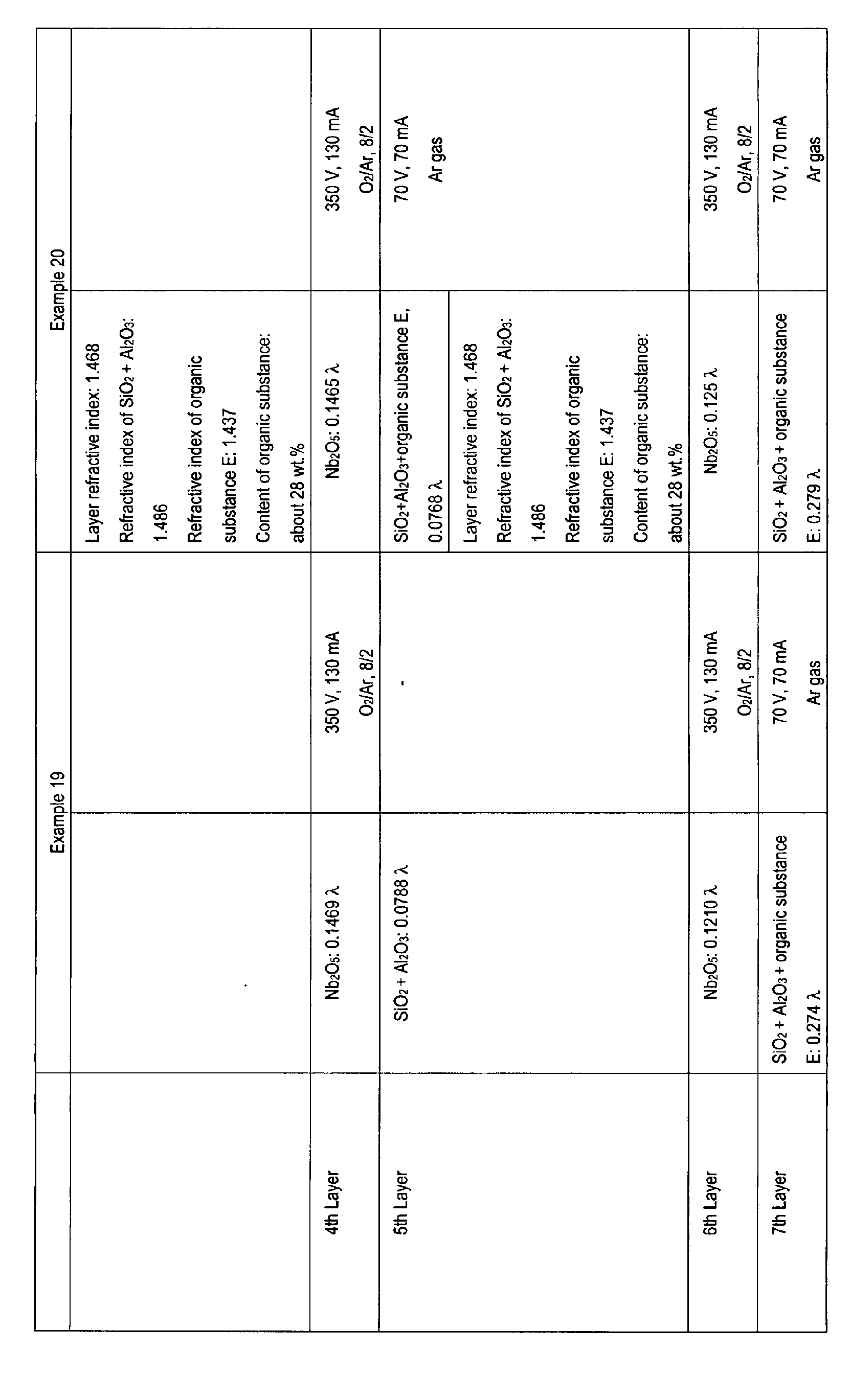
- One preferred embodiment of the layer constitution of the antireflection film formed on a plastic substrate in the invention is as follows:
- 1st layer: hybrid layer of SiO2 + Al2O3 + organic substance (layer thickness, 10 to 180 nm),
- 2nd layer: Nb2O5 layer (layer thickness, 1 to 25 nm),
- 3rd layer: SiO2 + Al2O3 layer (layer thickness, 10 to 50 nm),
- 4th layer: Nb2O5 layer (layer thickness, 10 to 55 nm),
- 5th layer: SiO2 + Al2O3 layer (layer thickness, 10 to 50 nm),
- 6th layer: Nb2O5 layer (layer thickness, 10 to 120 nm), and
- 7th layer: hybrid layer of SiO2 + Al2O3 + organic substance (layer thickness, 70 to 100 nm).
-
- The ranges of the layer thickness mentioned above are preferred ones for the impact resistance, adhesiveness, heat resistance and abrasion resistance of the optical element having an antireflection film formed on a plastic substrate.
- Another preferred embodiment of the layer constitution of the antireflection film is as follows:
- Basic layer: Nb layer (layer thickness, 1 to 5 nm),
- 1st layer: hybrid layer of SiO2 + Al2O3 + organic substance (layer thickness, 10 to 180 nm),
- 2nd layer: Nb2O5 layer (layer thickness, 10 to 55 nm),
- 3rd layer: SiO2 + Al2O3 layer (layer thickness, 10 to 50 nm),
- 4th layer: Nb2O5 layer (layer thickness, 10 to 55 nm),
- 5th layer: SiO2 + Al2O3 layer (layer thickness, 10 to 50 nm),
- 6th layer: Nb2O5 layer (layer thickness, 10 to 120 nm), and
- 7th layer: hybrid layer of SiO2 + Al2O3 + organic substance (layer thickness, 70 to 100 nm).
-
- The ranges of the layer thickness mentioned above are preferred ones for the impact resistance, adhesiveness, heat resistance and abrasion resistance of the optical element having an antireflection film formed on a plastic substrate. For better properties, at least one layer in the film constitution may be formed in an ion-assisted process.
- The preferred range of the refractive index of the hybrid layer of SiO2 + Al2O3 + organic substance is from 1.450 to 1.485 from the standpoint of obtaining good abrasion resistance and impact resistance.
- The material for the plastic substrate for use in the invention is not specifically limited, including, for example, methyl methacrylate homopolymers, copolymers of methyl methacrylate and one or more other monomers, diethylene glycol bisallyl carbonate homopolymers, copolymers of diethylene glycol bisallyl carbonate and one or more other monomers, sulfur-containing copolymers, halogen copolymers, polycarbonates, polystyrenes, polyvinyl chlorides, unsaturated polyesters, polyethylene terephthalates, polyurethanes, and polythiourethanes.
- The optical element of the invention may have a cured film between the plastic substrate and the basic layer.
- For the cured film, in general, a composition that comprises metal oxide colloid particles and an organosilicon compound of the following general formula (II) is used:
- Examples of the metal oxide colloid particles include those of tungsten oxide (WO3), zinc oxide (ZnO), silicon oxide (SiO2), aluminum oxide (Al2O3), titanium oxide (TiO2), zirconium oxide (ZrO2), tin oxide (SnO2), beryllium oxide (BeO), and antimony oxide (Sb2O5). These metal oxides may be used alone or be combined herein.
- Examples of the organosilicon compound of the general formula (II) include methyl silicate, ethyl silicate, n-propyl silicate, i-propyl silicate, n-butyl silicate, sec-butyl silicate, t-butyl silicate, tetraacetoxysilane, methyltrimethoxysilane, methyltriethoxysilane, methyltripropoxysilane, methyltriacetoxysilane, methyltributoxysilane, methyltripropoxysilane, methyltriamyloxysilane, methyltriphenoxysilane, methyltribenzyloxysilane, methyltriphenethyloxysilane, glycidoxymethyltrimethoxysilane, glycidoxymethyltriethoxysilane, α-glycidoxyethyltriethoxysilane, β-glycidoxyethyltrimethoxysilane, β-glycidoxyethyltriethoxysilane, α-glycidoxypropyltrimethoxysilane, α-glycidoxypropyltriethoxysilane, β-glycidoxypropyltrimethoxysilane, β-glycidoxypropyltriethoxysilane, γ-glycidoxypropyltrimethoxysilane, γ-glycidoxypropyltriethoxysilane, γ-glycidoxypropyltripropoxysilane, γ-glycidoxypropyltributoxysilane, γ-glycidoxypropyltriphenoxysilane, α-glycidoxybutyltrimethoxysilane, α-glycidoxybutyltriethoxysilane, β-glycidoxybutyltrimethoxysilane, β-glycidoxybutyltriethoxysilane, γ-glycidoxybutyltrimethoxysialne, γ-glycidoxybutyltriethoxysilane, δ-glycidoxybutyltrimethoxysilane, δ-glycidoxybutyltriethoxysilane, (3,4-epoxycyclohexyl)methyltrimethoxysilane, (3,4-epoxycyclohexyl)methyltriethoxysilane, β-(3,4-epoxycyclohexyl)ethyltrimethoxysilane, β-(3,4-epoxycyclohexyl)ethyltriethoxysilane, β-(3,4-epoxycyclohexyl)ethyltripropoxysilane, β-(3,4-epoxycyclohexyl)ethyltributoxysilane, β-(3,4-epoxycyclohexyl)ethyltriphenoxysilane, γ-(3,4-epoxycyclohexyl)propyltrimethoxysilane, γ-(3,4-epoxycyclohexyl)propyltriethoxysilane, δ-(3,4-epoxycyclohexyl)butyltrimethoxysilane, δ-(3,4-epoxycyclohexyl)butyltriethoxysilane, glycidoxymethylmethyldimethoxysilane, glycidoxymethylmethyldiethoxysilane, α-glycidoxyethylmethyldimethoxysilane, α-glycidoxyethylmethyldiethoxysilane, β-glycidoxyethylmethyldimethoxysilane, β-glycidoxyethylmethyldiethoxysilane, α-glycidoxypropylmethyldimethoxysilane, α-glycidoxypropylmethyldiethoxysilane, β-glycidoxypropylmethyldimethoxysilane, β-glycidoxypropylmethyldiethoxysilane, γ-glycidoxypropylmethyldimethoxysilane, γ-glycidoxypropylmethyldiethoxysilane, γ-glycidoxypropylmethyldipropoxysilane, γ-glycidoxypropylmethyldibutoxysilane, γ-glycidoxypropylmethyldiphenoxysilane, γ-glycidoxypropylethyldimethoxysilane, γ-glycidoxypropylethyldiethoxysilane, γ-glycidoxypropylvinyldimethoxysilane, γ-glycidoxypropylvinyldiethoxysilane, γ-glycidoxypropylphenyldimethoxysilane, γ-glycidoxypropylphenyldiethoxysilane, ethyltrimethoxysilane, ethyltriethoxysilane, vinyltrimethoxysilane, vinyltriacetoxysilane, vinyltrimethoxyethoxysilane, phenyltrimethoxysilane, phenyltriethoxysilane, phenyltriacetoxysilane, γ-chloropropyltrimethoxysilane, γ-chloropropyltriethoxysilane, γ-chloropropyltriacetoxysilane, 3,3,3-trifluoropropyltrimethoxysilane, γ-methacryloxypropyltrimethoxysilane, γ-mercaptopropyltrimethoxysilane, γ-mercaptopropyltriethoxysilane, β-cyanoethyltriethoxysilane, chloromethyltrimethoxysilane, chloromethyltriethoxysilane, N-(β-aminoethyl)-γ-aminopropyltrimethoxysilane, N-(β-aminoethyl)-γ-aminopropylmethyldimethoxysilane, γ-aminopropylmethyldimethoxysilane, N-(β-aminoethyl)-γ-aminopropyltriethoxysilane, N-(β-aminoethyl)-γ-aminopropylmethyldiethoxysilane, dimethyldimethoxysilane, phenylmethyldimethoxysilane, dimethyldiethoxysilane, phenylmethyldiethoxysilane, γ-chloropropylmethyldimethoxysilane, γ-chloropropylmethyldiethoxysilane, dimethyldiacetoxysilane, γ-methacryloxypropylmethyldimethoxysilane, γ-methacryloxypropylmethyldiethoxysilane, γ-mercaptopropylmethyldimethoxysilane, γ-mercaptopropylmethyldiethoxysilane, methylvinyldimethoxysilane, and methylvinyldiethoxysilane.
- The coating solution to form the cured film can be formulated in the conventionally known manner. If desired, a curing catalyst as well as various organic solvents and surfactants can be contained for the purposes of improving the wettability during the application and improving the smoothness of the cured film. In addition, UV absorbents, antioxidants, light stabilizers, anti-aging agents, etc. can be added so far as the desired physical properties of the coating composition and the cured film are achieved.
- The coating composition is cured by drying with hot air or by exposure to active energy rays. Preferably, it is cured in hot air at 70 to 200°C, more preferably at 90 to 150°C. Examples of the active energy rays include far-infrared rays, so that a damage by heat can be suppressed.
- Examples of the method for forming a cured film made of the coating composition on a substrate include a method in which the coating composition is applied onto the substrate. The application can be carried out by means of any ordinary method such as dipping, spin coating and spraying. In view of the face accuracy dipping or spin coating is especially preferred.
- The invention is described in more detail with reference to the following Examples, which, however, are not intended to restrict the invention.
- The physical properties of the optical elements obtained in the following Examples and Comparative Examples were measured according to the methods mentioned below.
- (1) Luminous transmittance: Using a spectrophotometer, U-3410 made by Hitachi, Ltd., the luminous transmittance, Y of a sample of a plastic lens having an antireflection film formed on both surfaces was measured.
- (2) Luminous reflectance: Using a spectrophotometer, U-3410 made by Hitachi, Ltd., the luminous reflectance, Z of a sample of a plastic lens having an antireflection film formed on both surfaces was measured.
- (3) Impact resistance: A plastic lens having a center thickness (CT) of 2.0 mm and a power of lens of -4.00 D was prepared and subjected to a drop ball test as defined by FDA (Food and Drug Administration). "O" indicates good samples; and "×" indicates rejected samples. The drop ball test was continued until the lens samples were broken, and the strength was confirmed as a maximum load. The weight of the ball was 14g.
- (4) Adhesiveness: Using a cutting tool, the surface of a plastic lens was cut to have 100 cross-cuts of 1 mm × 1 mm each. An adhesive tape, Cellotape was stuck on its cross-cut area, and peeled off at a stroke. The number of the remained cross-cuts was counted and shown in the following Tables, in which (number of remained cross-cuts)/100 indicates the adhesiveness.
- (5) Abrasion resistance:
The surface of a plastic lens was rubbed with steel wool
under a load of 1 kgf/cm2 applied thereto. After 10 strokes of
rubbing, the surface condition of the plastic lens was
evaluated according to the following criteria:
- UA: Scratched little.
- A: A few thin scratch marks found.
- B: Many thin scratch marks and a few thick scratch marks found.
- C: Many thin and thick scratch marks found.
- D: Almost completely peeled.
- (6) Heat resistance: A plastic lens was heated in a dry oven for 1 hour. The heating temperature at the start of the test was 60°C, and it was elevated at intervals of 5°C. The temperature at which it cracked was read.
- (7) Alkali resistance:
A plastic lens was dipped in an aqueous 10 % NaOH
solution at 20°C for 1 hour, and its surface condition was
evaluated according to the following criteria:
- UA: Changed little.
- A: A few peeled dots found.
- B: Many peeled dots found everywhere on the surface.
- C: Many peeled dots found everywhere on the surface, and a few peeled squares found.
- D: Almost completely peeled.
-
- 90 parts by weight of colloidal silica (Snowtex-40 available from Nissan Chemical Industries, Ltd.), 81.6 parts by weight of methyltrimethoxysilane and 176 parts by weight of γ-glycidoxypropyltrimethoxysilane as organosilicon compounds, 2.0 parts by weight of 0.5 N hydrochloric acid, 20 parts by weight of acetic acid, and 90 parts by weight of water were charged into a glass container, and the solution was stirred at room temperature for 8 hours. The resulting solution was left at room temperature for 16 hours to obtain a hydrolyzed solution. To this solution were added 120 parts by weight of isopropyl alcohol, 120 parts by weight of n-butyl alcohol, 16 parts by weight of aluminum acetylacetone, 0.2 parts by weight of a silicone surfactant, and 0.1 parts by weight of a UV absorbent. The mixture was stirred at room temperature for 8 hours, and then aged at room temperature for 24 hours to obtain a coating solution.
- A plastic lens substrate (made of diethylene glycol bisallyl carbonate, and having a refractive index of 1.50, a center thickness of 2.0 mm, a diameter of 70 mm and a power of lens of 0.00), which had been pretreated with an aqueous alkali solution, was dipped in the coating solution. After completion of dipping, the plastic lens was taken out at a pulling rate of 20 cm/min. Then, the plastic lens was heated at 120°C for 2 hours to form a cured film (hard coat layer A). Next, the resulting plastic lens was subjected to an ion gun pretreatment using an Ar gas under the condition of the ion acceleration voltage as shown in Tables 1 to 10.
- Next, under the conditions shown in Tables 1 to 10, an antireflection film composed of 1st to 7th layers was formed on the hard coat layer A to obtain plastic lenses.
- In forming the hybrid layer, the inorganic substance and the organic substance were almost simultaneously evaporated and deposited in a mode of controlled two-way vapor deposition. The organic substance was dissolved in an organic solvent, and the resulting solution was infiltrated into a sintered stainless steel-made filter (pore size, 80 to 100 µm, diameter: 18 mm, thickness: 3 mm). The ratio of the organic substance to the solvent was 1/4 by weight, and the content of the organic substance and the solvent was 1 ml per one filter chip. The filter was set in a vacuum evaporation chamber and heated at 250°C. However, since the organic substance E was vaporized in an external heating tank, and its vapor was introduced into the vapor deposition chamber using a gas valve and a mass flow controller, no filter chip was used.
- The structures of the products, organic substances A to E in the Tables are as follows.
- This is a reactive silicone oil, KF1001 (available from Shin-Etsu Silicone Co., Ltd.) of the general formula (a) in which the organic group is an epoxy group. The solvent is trimethylethylsilane, LS-865 (available from Shin-Etsu Chemical Co., Ltd.).
- This is a reactive silicone oil, X22-4741 (available from Shin-Etsu Silicone Co., Ltd.) of the general formula (a) in which the organic group is an epoxy group and a polyether group. The solvent is ethyl acetate.
- This is a reactive silicone oil, X22-8008 (available from Shin-Etsu Silicone Co., Ltd.) of the general formula (a) in which the organic group is an aminoalkyl group. The solvent is diethyl ether.
- This is polyoxyethylene monoacrylate, AE-400 (available from NOF Corporation). The solvent is ethyl acetate.
- This is polyethylene glycol glycidyl ether, E-400 (available from NOF Corporaiton). No solvent is used.
- The obtained plastic lenses were evaluated according to the test methods (1) to (7) mentioned above, and the results are shown in Tables 1 to 10. In the Tables, λ indicates the wavelength of the light applied, and λ = 500 nm. The refractive index of the hybrid layer was measured at λ = 500 nm.
- Plastic lenses were fabricated under the conditions shown in Tables 11 and 12, in which the hard coat layer and the functional film of the first to seventh layers were all formed of an inorganic substance only.
- The plastic lenses were evaluated according to the test methods (1) to (7) mentioned above, and the results are shown in Tables 11 and 12.
Layers, which were produced without an ion assisted process, are indicated in the following tables by the sign '-' in the column 'Ion gun setting'. These layers were deposited through conventional vapor deposition.


- As shown in Tables 1 to 10, the plastic lenses of Examples 1 to 20 had an extremely small luminous reflectance of from 0.70 to 0.82 % and had a large luminance transmittance of from 99.0 to 99.11 %. In addition, their impact resistance, adhesiveness, abrasion resistance, heat resistance and alkali resistance were good.
- As opposed to these, the plastic lenses of Comparative Examples 1 to 4 all had a high luminous reflectance of from 1.1 to 1.2 %, as in Tables 11 and 12. In addition, their impact resistance was low, and their adhesiveness, abrasion resistance, heat resistance and alkali resistance were lower than those in Examples 1 to 20.
- The above Examples 1 to 20 describe preferred embodiments of the present invention, the scope of which being defined by the appended claims. Further preferred embodiments of the present invention can be derived from the above Examples 1 to 20 by combining individual layers of different examples in a manner that is in accordance with the present invention.
- As described in detail hereinabove, the optical element of the invention has a good antireflection film of which the reflectance is small and the transmittance is large, and, in addition, it has the advantages of superior impact resistance, adhesiveness, heat resistance, abrasion resistance and alkali resistance, and its productivity is good.


Claims (22)
- An optical element having an antireflection film, which comprises a plastic substrate and an antireflection film comprising one or more layers obtainable through vacuum evaporation, wherein at least one layer of the antireflection film is a hybrid layer comprising an inorganic substance and an organic substance.
- The optical element having an antireflection film according to claim 1, wherein the hybrid layer is obtainable by means of an ion-assisted process.
- The optical element having an antireflection film according to claim 1 or 2, wherein the inorganic substance in the hybrid layer is SiO2.
- The optical element having an antireflection film according to claim 1 or 2, wherein the inorganic substance in the hybrid layer is SiO2 and Al2O3.
- The optical element having an antireflection film according to claim 1 or 2, wherein the inorganic substance in the hybrid layer is at least one inorganic oxide selected from SiO2, Al2O3, Nb2O5, Ta2O5, TiO2, ZrO2 and Y2O3.
- The optical element having an antireflection film according to any one of claims 1 to 5, wherein the organic substance in the hybrid layer is a modified silicone oil.
- The optical element having an antireflection film according to claim 6, wherein the modified silicone oil comprises one or more compounds having a structure of any of the following general formulae (a) to (d):(a) modified silicone oil having an organic group introduced into the side chains of polysiloxane:
 (b) modified silicone oil having an organic group introduced into both ends of polysiloxane:
 (c) modified silicone oil having an organic group introduced into one end of polysiloxane:
 (d) modified silicone oil having an organic group introduced into the side chains and both ends of polysiloxane:in the general formulae (a) to (d), m and n each independently indicate an integer of 0 or more; and in the general formula (c), R represents an alkyl group having from 1 to 10 carbon atoms, alkenyl group having from 2 to 10 carbon atoms, or an alkinyl group having from 2 to 10 carbon atoms.
- The optical element having an antireflection film according to claim 7, wherein the organic group is selected from an amino group, an epoxy group, a carboxyl group, a hydroxyl group, a hydroxyl group-containing hydrocarbon group having 1 to 15 carbon atoms, a (meth)acrylic group, a mercapto group, a phenol group, an alkoxy group having from 1 to 15 carbon atoms, a hydrocarbon group having 1 to 15 carbon atoms carrying one or more of the substituents listed above, and combinations thereof.
- The optical element having an antireflection film according to claim 7, wherein the organic group is selected from an alkyl group having from 1 to 15 carbon atoms, an ester group having from 2 to 15 carbon atoms, a methylstyryl group, a poly(C2-15 alkylene)ether group having 2 to 15 repeating units, an ester of a saturated or unsaturated fatty acid having 16 to 20 carbon atoms, and a hydrocarbon group having 1 to 15 carbon atoms that is substituted with one or more fluorine atoms.
- The optical element having an antireflection film according to any one of claims 6 to 9, wherein the modified silicone oil has a number-average molecular weight of from 250 to 6,000.
- The optical element having an antireflection film according to claim 1 or 2, wherein the organic substance in the hybrid layer is a compound of the following general formula (I):wherein x and z each independently indicate an integer of 0 or more; y indicates an integer of 1 or more; R1 to R6 each independently represent a hydrogen atom or an organic group selected from a methyl group, a hydrocarbon group having 0 to 15 carbon atoms optionally containing one or more functional groups selected from an epoxy group, an amino group, a (meth)acrylic group, a hydroxyl group, a hydrocarbon group having 1 to 15 carbon atoms containing a carbonyl group, a vinyl group, a thiol group, a carbon-carbon triple bond-containing hydrocarbon group having 1 to 15 carbon atoms, an alkoxysilane group having from 1 to 15 carbon atoms, an alkylamino group having from 1 to 15 carbon atoms and a cyclic alkyl group having from 5 to 8 carbon atoms.

- The optical element having an antireflection film according to claim 11, wherein at least one of R1 to R6 is a sorbitan residue or a sorbitan ester residue.
- The optical element having an antireflection film according to claim 11, wherein the compound of the general formula (I) is polyethylene glycol monobutyl monoglycidyl ether, polyethylene glycol diglycidyl ether, polyoxyethylene α,ω-bis-3-aminopropyl ether, polyethylene glycol sorbitan monolaurate, polyethylene glycol sorbitan monooleate or polyoxyethylene monoacrylate.
- The optical element having an antireflection film according to any one of claims 11 to 13, wherein the compound of the general formula (I) has a number-average molecular weight of from 250 to 6,000.
- The optical element having an antireflection film according to any one of claims 1 to 14, wherein the content of the organic substance in the hybrid layer in the film is from 0.02 % by weight to 70 % by weight.
- The optical element according to any one of claims 1 to 15, which has a basic layer having a thickness of from 1 to 5 nm and comprising at least one selected from nickel (Ni), silver (Ag), platinum (Pt), niobium (Nb) and titanium (Ti), formed between the plastic substrate and the antireflection film.
- The optical element having an antireflection film according to any one of claims 1 to 16, wherein the antireflection film is so configured that one hybrid layer is nearest to the plastic substrate and another hybrid layer, which may be the same or which may be different from the first hybrid layer, is remotest from it.
- The optical element according to claim 17, wherein the antireflection film comprises the following layers formed in that order on the plastic substrate:1st layer: hybrid layer of SiO2 + Al2O3 + organic substance (layer thickness, 10 to 180 nm),2nd layer: Nb2O5 layer (layer thickness, 1 to 25 nm),3rd layer: SiO2 + Al2O3 layer (layer thickness, 10 to 50 nm),4th layer: Nb2O5 layer (layer thickness, 10 to 55 nm),5th layer: SiO2 + Al2O3 layer (layer thickness, 10 to 50 nm),6th layer: Nb2O5 layer (layer thickness, 10 to 120 nm), and7th layer: hybrid layer of SiO2 + Al2O3 + organic substance (layer thickness, 70 to 100 nm).
- Method for forming the optical element having an antireflection film according to any one of claims 1 to 18, wherein the antireflection film is formed through vacuum evaporation.
- Method according to claim 19, wherein at least one of the hybrid layers is formed using an ion-assisted process.
- Use of the optical element having an antireflection film according to any one of claims 1 to 18 for the preparation of a spectacle.
- Spectacle comprising the optical element having an antireflection film according to any one of claims 1 to 18.
Priority Applications (1)
| Application Number | Priority Date | Filing Date | Title |
|---|---|---|---|
| EP20100173667 EP2249187A1 (en) | 2001-10-25 | 2002-10-24 | Optical element having antireflection film |
Applications Claiming Priority (2)
| Application Number | Priority Date | Filing Date | Title |
|---|---|---|---|
| JP2001327252 | 2001-10-25 | ||
| JP2001327252 | 2001-10-25 |
Related Child Applications (1)
| Application Number | Title | Priority Date | Filing Date |
|---|---|---|---|
| EP10173667.6 Division-Into | 2010-08-23 |
Publications (4)
| Publication Number | Publication Date |
|---|---|
| EP1306695A2 true EP1306695A2 (en) | 2003-05-02 |
| EP1306695A3 EP1306695A3 (en) | 2006-06-28 |
| EP1306695B1 EP1306695B1 (en) | 2010-10-13 |
| EP1306695B9 EP1306695B9 (en) | 2010-12-22 |
Family
ID=19143508
Family Applications (2)
| Application Number | Title | Priority Date | Filing Date |
|---|---|---|---|
| EP20020023756 Expired - Lifetime EP1306695B9 (en) | 2001-10-25 | 2002-10-24 | Optical element having antireflection film |
| EP20100173667 Withdrawn EP2249187A1 (en) | 2001-10-25 | 2002-10-24 | Optical element having antireflection film |
Family Applications After (1)
| Application Number | Title | Priority Date | Filing Date |
|---|---|---|---|
| EP20100173667 Withdrawn EP2249187A1 (en) | 2001-10-25 | 2002-10-24 | Optical element having antireflection film |
Country Status (11)
| Country | Link |
|---|---|
| US (1) | US6919134B2 (en) |
| EP (2) | EP1306695B9 (en) |
| KR (1) | KR100511837B1 (en) |
| CN (1) | CN1276273C (en) |
| AT (1) | ATE484764T1 (en) |
| AU (1) | AU2002301541B8 (en) |
| CA (1) | CA2408113C (en) |
| DE (1) | DE60237951D1 (en) |
| ES (1) | ES2351435T3 (en) |
| HU (1) | HUP0203631A3 (en) |
| TW (1) | TW571114B (en) |
Cited By (8)
| Publication number | Priority date | Publication date | Assignee | Title |
|---|---|---|---|---|
| EP1324078A2 (en) * | 2001-12-28 | 2003-07-02 | Hoya Corporation | Hybrid film, antireflection film comprising it, optical product, and method for restoring the defogging property of hybrid film |
| EP1433809A1 (en) * | 2002-12-26 | 2004-06-30 | Hoya Corporation | Optical member having antireflection film |
| FR2859485A1 (en) * | 2003-09-04 | 2005-03-11 | Essilor Int | METHOD FOR PRODUCING AN ANTI-REFLECTIVE TREATMENT ON AN OPTICAL SUBSTRATE, OPTICAL SUBSTRATE OBTAINED BY THIS METHOD AND DEVICE FOR IMPLEMENTING THE METHOD |
| FR2913116A1 (en) * | 2007-02-23 | 2008-08-29 | Essilor Int | METHOD FOR MANUFACTURING OPTICAL ARTICLE COATED WITH AN ANTI-REFLECTIVE OR REFLECTIVE COATING HAVING IMPROVED ADHESION AND ABRASION RESISTANCE PROPERTIES |
| EP2078765A1 (en) * | 2006-09-29 | 2009-07-15 | Hoya Corporation | Vapor deposition material, process for producing optical member or plastic lens for spectacle with use thereof, and plastic lens for spectacle |
| US8318245B2 (en) | 2007-02-23 | 2012-11-27 | Essilor International (Compagnie Generale D'optique) | Method for producing an optical article coated with an antireflection or a reflective coating having improved adhesion and abrasion resistance properties |
| WO2017021670A1 (en) * | 2015-08-05 | 2017-02-09 | Essilor International (Compagnie Générale d'Optique) | Item having improved thermomechanical properties, comprising an organic-inorganic layer |
| EP3185050A1 (en) | 2015-12-23 | 2017-06-28 | Essilor International (Compagnie Générale D'Optique) | Optical article comprising a multilayered interferential coating obtained from an organic precursor or a mixture of organic precursors |
Families Citing this family (37)
| Publication number | Priority date | Publication date | Assignee | Title |
|---|---|---|---|---|
| US6562466B2 (en) | 2001-07-02 | 2003-05-13 | Essilor International Compagnie Generale D'optique | Process for transferring a coating onto a surface of a lens blank |
| JP2005292462A (en) * | 2004-03-31 | 2005-10-20 | Konica Minolta Opto Inc | Optical element having dielectric multilayer film |
| CN100395613C (en) * | 2004-08-07 | 2008-06-18 | 鸿富锦精密工业(深圳)有限公司 | Light permeating plate |
| US20080006368A9 (en) * | 2005-02-01 | 2008-01-10 | Peiqi Jiang | Process for applying a coating onto a surface of a lens substrate |
| CN100581810C (en) | 2005-03-30 | 2010-01-20 | 鸿富锦精密工业(深圳)有限公司 | Plastic filming module assembly and method for manufacturing same |
| US20060219347A1 (en) * | 2005-04-04 | 2006-10-05 | Essilor International Compagnie Generale D'optique | Process for transferring coatings onto a surface of a lens substrate with most precise optical quality |
| TWI292340B (en) | 2005-07-13 | 2008-01-11 | Ind Tech Res Inst | Antireflective transparent zeolite hardcoat film, method for fabricating the same, and solution capable of forming said transparent zeolite film |
| US20070035070A1 (en) * | 2005-08-15 | 2007-02-15 | Essilor International Compagnie Generale D'optique | Inflatable membrane pressing apparatus for a film or coating application or lamination process |
| US20070034321A1 (en) * | 2005-08-15 | 2007-02-15 | Essilor International Compagnie Generale D'optique | System and process for making a coated article |
| US20070034322A1 (en) * | 2005-08-15 | 2007-02-15 | Essilor International Compagnie Generale D'optique | System and process for making a coated article |
| WO2007043700A1 (en) * | 2005-10-14 | 2007-04-19 | Fujifilm Corporation | Anti-reflection film, and polarizing plate and image display device using the same |
| KR100831238B1 (en) * | 2005-12-01 | 2008-05-22 | 주식회사 엘지화학 | Silicone-based hard coating materials with for middle and high refractive index substrate, method for preparing the same, and optical lens prepared therefrom |
| KR100725793B1 (en) | 2005-12-26 | 2007-06-08 | 제일모직주식회사 | Hardmask composition coated under photoresist and process of producing integrated circuit devices using thereof |
| KR100725794B1 (en) | 2005-12-26 | 2007-06-08 | 제일모직주식회사 | Hardmask composition coated under photoresist and process of producing integrated circuit devices using thereof |
| KR100947720B1 (en) * | 2006-10-18 | 2010-03-16 | 주식회사 엘지화학 | Silicone based coating composition having excellent abrasion resistance, transparency and dyeability, a method for the preparation thereof, and an optical lenz coated by said coating composition |
| BRPI0720867A2 (en) * | 2006-12-29 | 2014-03-04 | 3M Innovative Properties Company. | METHOD FOR MANUFACTURING INORGANIC OR HYBRID / ORGANIC HYBRID MOVIES |
| US7981471B2 (en) * | 2007-05-18 | 2011-07-19 | Hoya Corporation | Processes for producing thin films and optical members |
| TWI425252B (en) * | 2008-03-26 | 2014-02-01 | Nat Applied Res Laboratories | Reflective film and method for manufacturing the same |
| KR20110033210A (en) * | 2008-06-30 | 2011-03-30 | 쓰리엠 이노베이티브 프로퍼티즈 컴파니 | Method of making inorganic or inorganic/organic hybrid barrier films |
| US8163357B2 (en) * | 2009-03-26 | 2012-04-24 | Signet Armorlite, Inc. | Scratch-resistant coatings with improved adhesion to inorganic thin film coatings |
| EP2426519A1 (en) * | 2009-05-01 | 2012-03-07 | Sustainable Titania Technology Incorporated | Agent for increasing amount of visible light transmitted by light-transmitting base and process for producing highly light-transmitting base with the same |
| CA2793855A1 (en) * | 2010-03-22 | 2011-09-29 | Luxottica Us Holdings Corporation | Ion beam assisted deposition of ophthalmic lens coatings |
| US8728636B2 (en) | 2010-12-13 | 2014-05-20 | Southwall Technologies Inc. | Insulating glass unit with crack-resistant low-emissivity suspended film |
| US8530011B2 (en) | 2010-12-13 | 2013-09-10 | Southwall Technologies Inc. | Insulating glass unit with crack-resistant low-emissivity suspended film |
| KR101836307B1 (en) | 2011-05-06 | 2018-03-09 | 엘지이노텍 주식회사 | Optical member, solar cell apparatus having the same and method of fabricating the same |
| FR2985255B1 (en) | 2011-12-28 | 2015-08-07 | Ecole Polytech | COATED ARTICLE WITH AN INTERFERENTIAL COATING HAVING STABLE PROPERTIES IN TIME. |
| CN104101918B (en) * | 2013-04-03 | 2017-03-01 | 法国圣戈班玻璃公司 | A kind of optical anti-reflective film and preparation method thereof and optical module |
| FR3007024A1 (en) * | 2013-06-14 | 2014-12-19 | Essilor Int | COATED ARTICLE WITH A SILICO-ORGANIC LAYER IMPROVING THE PERFORMANCE OF AN EXTERNAL COATING |
| CN105255381A (en) * | 2014-01-09 | 2016-01-20 | 苏州斯迪克新材料科技股份有限公司 | Scratch resistant anti-dazzle protection film |
| JP6443440B2 (en) * | 2014-03-06 | 2018-12-26 | コニカミノルタ株式会社 | Laminated film and method for producing the same |
| WO2015166144A1 (en) | 2014-04-28 | 2015-11-05 | Corporation De L'ecole Polytechnique De Montreal | Article having optimised thermomechanical properties, comprising a layer of titano-organic nature |
| FR3039827B1 (en) * | 2015-08-05 | 2022-03-18 | Essilor Int | ARTICLE WITH OPTIMIZED ADHESION PROPERTIES INCLUDING A SILICO-ORGANIC LAYER |
| FR3045672B1 (en) * | 2015-12-18 | 2018-03-16 | Corporation De L'ecole Polytechnique De Montreal | ARTICLE COMPRISING AN ORGANIC-INORGANIC LAYER OF LOW REFRACTIVE INDEX |
| FR3051000B1 (en) * | 2016-05-09 | 2018-06-01 | Corporation De L'ecole Polytechnique De Montreal | ARTICLE COMPRISING A LOW ORGANIC-INORGANIC COATING OF REFRACTION INDEX OBTAINED BY AN OBLIQUE ANGLE DEPOSITION |
| EP3287818B1 (en) | 2016-08-23 | 2020-11-11 | Corporation de L'Ecole Polytechnique de Montreal | Ophthalmic lens having increased resistance to hot and humid environment |
| JP2020083700A (en) * | 2018-11-26 | 2020-06-04 | コニカミノルタ株式会社 | Optical member and method for manufacturing optical member |
| EP3693766A1 (en) * | 2019-02-05 | 2020-08-12 | Corporation de L'Ecole Polytechnique de Montreal | Article coated with a low refractive index layer based on fluorinated organosilicon compounds |
Citations (4)
| Publication number | Priority date | Publication date | Assignee | Title |
|---|---|---|---|---|
| JPS63141001A (en) | 1986-12-04 | 1988-06-13 | Hoya Corp | Production of plastic lens |
| WO1995024275A2 (en) | 1994-03-03 | 1995-09-14 | Diamonex, A Unit Of Monsanto Company | Highly abrasion-resistant, flexible coatings for soft substrates |
| WO1998033077A2 (en) | 1997-01-27 | 1998-07-30 | Haaland Peter D | Coatings, methods and apparatus for reducing reflection from optical substrates |
| EP1123905A2 (en) | 2000-02-10 | 2001-08-16 | C. Itoh Fine Chemical Co. Ltd. | Process for forming an optical composite film and for producing optical articles from the same |
Family Cites Families (25)
| Publication number | Priority date | Publication date | Assignee | Title |
|---|---|---|---|---|
| US4047804A (en) * | 1973-12-26 | 1977-09-13 | Polaroid Corporation | Anti-reflection coatings for photographic bases |
| JPS6381033A (en) * | 1986-09-25 | 1988-04-11 | Toray Ind Inc | Antireflection article and manufacture thereof |
| JPS6385701A (en) * | 1986-09-30 | 1988-04-16 | Toray Ind Inc | Antireflection article and its production |
| US4929278A (en) * | 1988-01-26 | 1990-05-29 | United States Department Of Energy | Sol-gel antireflective coating on plastics |
| US5181142A (en) * | 1988-06-10 | 1993-01-19 | Asahi Kogaku Kogyo Kabushiki Kaisha | Plastic lens and method of forming an anti-reflecting layer on a plastic lens |
| US5181141A (en) * | 1989-03-31 | 1993-01-19 | Hoya Corporation | Anti-reflection optical element |
| US5104692A (en) * | 1990-04-20 | 1992-04-14 | Pilkington Visioncare Holdings, Inc. | Two-layer antireflective coating applied in solution |
| FR2680583B1 (en) * | 1991-08-22 | 1993-10-08 | Commissariat A Energie Atomique | MATERIAL HAVING ANTI-REFLECTIVE, HYDROPHOBIC AND ABRASION RESISTANCE PROPERTIES AND METHOD FOR DEPOSITING AN ANTI-REFLECTIVE, HYDROPHOBIC AND ABRASION RESISTANT LAYER ON A SUBSTRATE. |
| US5194990A (en) * | 1991-10-07 | 1993-03-16 | Ford Motor Company | Low color purity, anti-reflection coatings for transparent glazings oriented at high angles of incidence |
| JPH06220428A (en) * | 1993-01-28 | 1994-08-09 | Toray Ind Inc | Surface-modified antifogging film |
| JPH08113760A (en) * | 1994-10-14 | 1996-05-07 | Seiko Epson Corp | Coating composition |
| JP3228658B2 (en) * | 1995-06-26 | 2001-11-12 | ジーイー東芝シリコーン株式会社 | Surface treatment method |
| JP3694882B2 (en) * | 1995-10-30 | 2005-09-14 | セイコーエプソン株式会社 | Antifogging article having antireflection performance and method for producing the same |
| US5990984A (en) * | 1995-11-16 | 1999-11-23 | Viratec Thin Films, Inc. | Coated polymer substrate with matching refractive index and method of making the same |
| TW376408B (en) * | 1995-12-01 | 1999-12-11 | Nissan Chemical Ind Ltd | Coating film having water repellency and low refractive index |
| FR2748743B1 (en) * | 1996-05-14 | 1998-06-19 | Saint Gobain Vitrage | GLASS WITH ANTI-REFLECTIVE COATING |
| US6210858B1 (en) * | 1997-04-04 | 2001-04-03 | Fuji Photo Film Co., Ltd. | Anti-reflection film and display device using the same |
| JPH10324846A (en) * | 1997-05-26 | 1998-12-08 | Seiko Epson Corp | Composition for use in coating, laminated product and lens for eyeglass |
| JPH11130982A (en) * | 1997-09-01 | 1999-05-18 | Seiko Epson Corp | Coating composition, production thereof, and laminate |
| JP3938636B2 (en) * | 1998-02-25 | 2007-06-27 | Hoya株式会社 | High refractive index plastic lens and manufacturing method thereof |
| DE60038477T2 (en) * | 1999-09-28 | 2009-06-04 | Fujifilm Corp. | Anti-reflection coating, polarizing plate provided therewith, and image display device with the anti-reflection coating or the polarizing plate |
| JP4271839B2 (en) * | 1999-09-28 | 2009-06-03 | 富士フイルム株式会社 | Antireflection film, polarizing plate, and image display device using the same |
| JP3982967B2 (en) * | 1999-12-28 | 2007-09-26 | 触媒化成工業株式会社 | Transparent film-forming coating solution, transparent film-coated substrate and display device |
| KR100644269B1 (en) * | 2000-02-21 | 2006-11-13 | 도레이새한 주식회사 | Producing method of hybrid antireflection film |
| JP3510845B2 (en) * | 2000-08-29 | 2004-03-29 | Hoya株式会社 | Optical member having antireflection film |
-
2002
- 2002-10-15 AU AU2002301541A patent/AU2002301541B8/en not_active Ceased
- 2002-10-15 CA CA002408113A patent/CA2408113C/en not_active Expired - Fee Related
- 2002-10-18 KR KR10-2002-0063798A patent/KR100511837B1/en not_active IP Right Cessation
- 2002-10-23 TW TW91124443A patent/TW571114B/en not_active IP Right Cessation
- 2002-10-24 ES ES02023756T patent/ES2351435T3/en not_active Expired - Lifetime
- 2002-10-24 AT AT02023756T patent/ATE484764T1/en not_active IP Right Cessation
- 2002-10-24 DE DE60237951T patent/DE60237951D1/en not_active Expired - Lifetime
- 2002-10-24 EP EP20020023756 patent/EP1306695B9/en not_active Expired - Lifetime
- 2002-10-24 EP EP20100173667 patent/EP2249187A1/en not_active Withdrawn
- 2002-10-25 HU HU0203631A patent/HUP0203631A3/en unknown
- 2002-10-25 US US10/279,931 patent/US6919134B2/en not_active Expired - Fee Related
- 2002-10-25 CN CNB021471819A patent/CN1276273C/en not_active Expired - Fee Related
Patent Citations (4)
| Publication number | Priority date | Publication date | Assignee | Title |
|---|---|---|---|---|
| JPS63141001A (en) | 1986-12-04 | 1988-06-13 | Hoya Corp | Production of plastic lens |
| WO1995024275A2 (en) | 1994-03-03 | 1995-09-14 | Diamonex, A Unit Of Monsanto Company | Highly abrasion-resistant, flexible coatings for soft substrates |
| WO1998033077A2 (en) | 1997-01-27 | 1998-07-30 | Haaland Peter D | Coatings, methods and apparatus for reducing reflection from optical substrates |
| EP1123905A2 (en) | 2000-02-10 | 2001-08-16 | C. Itoh Fine Chemical Co. Ltd. | Process for forming an optical composite film and for producing optical articles from the same |
Non-Patent Citations (1)
| Title |
|---|
| SCHILLER ET AL.: "PICVD : A novel technique for hard- and AR-coating of spectacles", PROCEEDINGS OF SPIE, vol. 3738, May 1999 (1999-05-01), pages 30 - 33, XP008083678 |
Cited By (21)
| Publication number | Priority date | Publication date | Assignee | Title |
|---|---|---|---|---|
| EP1324078A2 (en) * | 2001-12-28 | 2003-07-02 | Hoya Corporation | Hybrid film, antireflection film comprising it, optical product, and method for restoring the defogging property of hybrid film |
| EP1324078A3 (en) * | 2001-12-28 | 2004-01-14 | Hoya Corporation | Hybrid film, antireflection film comprising it, optical product, and method for restoring the defogging property of hybrid film |
| US6958172B2 (en) | 2001-12-28 | 2005-10-25 | Hoya Corporation | Hybrid film, antireflection film comprising it, optical product, and method for restoring the defogging property of hybrid film |
| EP1433809A1 (en) * | 2002-12-26 | 2004-06-30 | Hoya Corporation | Optical member having antireflection film |
| AU2003268585B2 (en) * | 2002-12-26 | 2005-01-20 | Hoya Corporation | Optical member having antireflection film |
| US7318959B2 (en) | 2002-12-26 | 2008-01-15 | Hoya Corporation | Optical element having antireflection film |
| FR2859485A1 (en) * | 2003-09-04 | 2005-03-11 | Essilor Int | METHOD FOR PRODUCING AN ANTI-REFLECTIVE TREATMENT ON AN OPTICAL SUBSTRATE, OPTICAL SUBSTRATE OBTAINED BY THIS METHOD AND DEVICE FOR IMPLEMENTING THE METHOD |
| WO2005024087A1 (en) * | 2003-09-04 | 2005-03-17 | Essilor International (Compagnie Generale D'optique) | Method for treating antireflection coatings on an optical substrate, the thus obtained optical substrate and device for carrying gout said method |
| US10011522B2 (en) | 2003-09-04 | 2018-07-03 | Essilor International | Method for treating antireflection coatings on an optical substrate, the thus obtained optical substrate and device for carrying gout said method |
| EP2078765A1 (en) * | 2006-09-29 | 2009-07-15 | Hoya Corporation | Vapor deposition material, process for producing optical member or plastic lens for spectacle with use thereof, and plastic lens for spectacle |
| EP2078765A4 (en) * | 2006-09-29 | 2010-06-02 | Hoya Corp | Vapor deposition material, process for producing optical member or plastic lens for spectacle with use thereof, and plastic lens for spectacle |
| JP5043851B2 (en) * | 2006-09-29 | 2012-10-10 | Hoya株式会社 | Vapor deposition material, optical member using the same, method for producing plastic lens for spectacles, and plastic lens for spectacles |
| WO2008107325A1 (en) * | 2007-02-23 | 2008-09-12 | Essilor International (Compagnie Generale D'optique) | Process for manufacturing an optical article coated with an antireflection or reflective coating having improved adhesion and abrasion-resistance properties |
| US8318245B2 (en) | 2007-02-23 | 2012-11-27 | Essilor International (Compagnie Generale D'optique) | Method for producing an optical article coated with an antireflection or a reflective coating having improved adhesion and abrasion resistance properties |
| AU2008223906B2 (en) * | 2007-02-23 | 2013-09-05 | Essilor International | Process for manufacturing an optical article coated with an antireflection or reflective coating having improved adhesion and abrasion-resistance properties |
| US8846140B2 (en) | 2007-02-23 | 2014-09-30 | Essilor International (Compagnie Generale D'optique) | Method for producing an optical article coated with an antireflection or a reflective coating having improved adhesion and abrasion resistance properties |
| FR2913116A1 (en) * | 2007-02-23 | 2008-08-29 | Essilor Int | METHOD FOR MANUFACTURING OPTICAL ARTICLE COATED WITH AN ANTI-REFLECTIVE OR REFLECTIVE COATING HAVING IMPROVED ADHESION AND ABRASION RESISTANCE PROPERTIES |
| WO2017021670A1 (en) * | 2015-08-05 | 2017-02-09 | Essilor International (Compagnie Générale d'Optique) | Item having improved thermomechanical properties, comprising an organic-inorganic layer |
| FR3039828A1 (en) * | 2015-08-05 | 2017-02-10 | Essilor Int | ARTICLE WITH IMPROVED THERMOMECHANICAL PROPERTIES COMPRISING A LAYER OF ORGANIC-INORGANIC NATURE |
| US11707921B2 (en) | 2015-08-05 | 2023-07-25 | Essilor International | Item having improved thermomechanical properties, comprising an organic-inorganic layer |
| EP3185050A1 (en) | 2015-12-23 | 2017-06-28 | Essilor International (Compagnie Générale D'Optique) | Optical article comprising a multilayered interferential coating obtained from an organic precursor or a mixture of organic precursors |
Also Published As
| Publication number | Publication date |
|---|---|
| ES2351435T3 (en) | 2011-02-04 |
| EP1306695B1 (en) | 2010-10-13 |
| TW571114B (en) | 2004-01-11 |
| EP1306695B9 (en) | 2010-12-22 |
| AU2002301541B8 (en) | 2005-07-14 |
| AU2002301541B2 (en) | 2005-04-28 |
| KR100511837B1 (en) | 2005-09-02 |
| CA2408113C (en) | 2005-10-04 |
| EP1306695A3 (en) | 2006-06-28 |
| US20030198818A1 (en) | 2003-10-23 |
| CN1276273C (en) | 2006-09-20 |
| HUP0203631A3 (en) | 2007-05-29 |
| US20040151918A9 (en) | 2004-08-05 |
| DE60237951D1 (en) | 2010-11-25 |
| CN1414398A (en) | 2003-04-30 |
| ATE484764T1 (en) | 2010-10-15 |
| CA2408113A1 (en) | 2003-04-25 |
| EP2249187A1 (en) | 2010-11-10 |
| HUP0203631A2 (en) | 2003-06-28 |
| HU0203631D0 (en) | 2002-12-28 |
| US6919134B2 (en) | 2005-07-19 |
| KR20030033938A (en) | 2003-05-01 |
Similar Documents
| Publication | Publication Date | Title |
|---|---|---|
| US6919134B2 (en) | Optical element having antireflection film | |
| US6958172B2 (en) | Hybrid film, antireflection film comprising it, optical product, and method for restoring the defogging property of hybrid film | |
| US6693747B2 (en) | Optical element having antireflection film | |
| EP0278060B1 (en) | Anti-reflection optical article and process of producing the same | |
| JP3201654B2 (en) | Coating composition | |
| JP5285300B2 (en) | Optical member | |
| JPH0627301A (en) | Optical member having cured film | |
| EP3136139A1 (en) | Eyeglass lens | |
| JP4362032B2 (en) | Optical member having antireflection film and method for producing the same | |
| JPH08198985A (en) | Optical member having cured coating film | |
| WO2022209092A1 (en) | Eyeglass lens and eyeglasses | |
| WO2022209091A1 (en) | Spectacle lens and spectacles | |
| JP2003255107A (en) | Hybrid thin film, antireflection film and optical member comprising the same, and method for restoring defogging performance of hybrid thin film | |
| WO2023080233A1 (en) | Eyeglass lens and eyeglasses |
Legal Events
| Date | Code | Title | Description |
|---|---|---|---|
| PUAI | Public reference made under article 153(3) epc to a published international application that has entered the european phase |
Free format text: ORIGINAL CODE: 0009012 |
|
| AK | Designated contracting states |
Designated state(s): AT BE BG CH CY CZ DE DK EE ES FI FR GB GR IE IT LI LU MC NL PT SE SK TR |
|
| AX | Request for extension of the european patent |
Extension state: AL LT LV MK RO SI |
|
| RIN1 | Information on inventor provided before grant (corrected) |
Inventor name: SHINDE, KENICHI Inventor name: SHIRAKAWA, HIROSHI Inventor name: MITSUISHI, TAKESHI |
|
| PUAL | Search report despatched |
Free format text: ORIGINAL CODE: 0009013 |
|
| AK | Designated contracting states |
Kind code of ref document: A3 Designated state(s): AT BE BG CH CY CZ DE DK EE ES FI FR GB GR IE IT LI LU MC NL PT SE SK TR |
|
| AX | Request for extension of the european patent |
Extension state: AL LT LV MK RO SI |
|
| 17P | Request for examination filed |
Effective date: 20061120 |
|
| AKX | Designation fees paid |
Designated state(s): AT BE BG CH CY CZ DE DK EE ES FI FR GB GR IE IT LI LU MC NL PT SE SK TR |
|
| TPAC | Observations filed by third parties |
Free format text: ORIGINAL CODE: EPIDOSNTIPA |
|
| 17Q | First examination report despatched |
Effective date: 20080806 |
|
| GRAP | Despatch of communication of intention to grant a patent |
Free format text: ORIGINAL CODE: EPIDOSNIGR1 |
|
| GRAS | Grant fee paid |
Free format text: ORIGINAL CODE: EPIDOSNIGR3 |
|
| GRAA | (expected) grant |
Free format text: ORIGINAL CODE: 0009210 |
|
| AK | Designated contracting states |
Kind code of ref document: B1 Designated state(s): AT BE BG CH CY CZ DE DK EE ES FI FR GB GR IE IT LI LU MC NL PT SE SK TR |
|
| REG | Reference to a national code |
Ref country code: GB Ref legal event code: FG4D |
|
| REG | Reference to a national code |
Ref country code: CH Ref legal event code: EP |
|
| REG | Reference to a national code |
Ref country code: IE Ref legal event code: FG4D |
|
| REF | Corresponds to: |
Ref document number: 60237951 Country of ref document: DE Date of ref document: 20101125 Kind code of ref document: P |
|
| REG | Reference to a national code |
Ref country code: ES Ref legal event code: FG2A Effective date: 20110125 |
|
| REG | Reference to a national code |
Ref country code: NL Ref legal event code: VDEP Effective date: 20101013 |
|
| PG25 | Lapsed in a contracting state [announced via postgrant information from national office to epo] |
Ref country code: BG Free format text: LAPSE BECAUSE OF FAILURE TO SUBMIT A TRANSLATION OF THE DESCRIPTION OR TO PAY THE FEE WITHIN THE PRESCRIBED TIME-LIMIT Effective date: 20110113 Ref country code: SE Free format text: LAPSE BECAUSE OF FAILURE TO SUBMIT A TRANSLATION OF THE DESCRIPTION OR TO PAY THE FEE WITHIN THE PRESCRIBED TIME-LIMIT Effective date: 20101013 Ref country code: NL Free format text: LAPSE BECAUSE OF FAILURE TO SUBMIT A TRANSLATION OF THE DESCRIPTION OR TO PAY THE FEE WITHIN THE PRESCRIBED TIME-LIMIT Effective date: 20101013 Ref country code: MC Free format text: LAPSE BECAUSE OF NON-PAYMENT OF DUE FEES Effective date: 20101031 Ref country code: PT Free format text: LAPSE BECAUSE OF FAILURE TO SUBMIT A TRANSLATION OF THE DESCRIPTION OR TO PAY THE FEE WITHIN THE PRESCRIBED TIME-LIMIT Effective date: 20110214 Ref country code: AT Free format text: LAPSE BECAUSE OF FAILURE TO SUBMIT A TRANSLATION OF THE DESCRIPTION OR TO PAY THE FEE WITHIN THE PRESCRIBED TIME-LIMIT Effective date: 20101013 Ref country code: FI Free format text: LAPSE BECAUSE OF FAILURE TO SUBMIT A TRANSLATION OF THE DESCRIPTION OR TO PAY THE FEE WITHIN THE PRESCRIBED TIME-LIMIT Effective date: 20101013 |
|
| REG | Reference to a national code |
Ref country code: CH Ref legal event code: PL |
|
| PG25 | Lapsed in a contracting state [announced via postgrant information from national office to epo] |
Ref country code: BE Free format text: LAPSE BECAUSE OF FAILURE TO SUBMIT A TRANSLATION OF THE DESCRIPTION OR TO PAY THE FEE WITHIN THE PRESCRIBED TIME-LIMIT Effective date: 20101013 Ref country code: GR Free format text: LAPSE BECAUSE OF FAILURE TO SUBMIT A TRANSLATION OF THE DESCRIPTION OR TO PAY THE FEE WITHIN THE PRESCRIBED TIME-LIMIT Effective date: 20110114 |
|
| PG25 | Lapsed in a contracting state [announced via postgrant information from national office to epo] |
Ref country code: EE Free format text: LAPSE BECAUSE OF FAILURE TO SUBMIT A TRANSLATION OF THE DESCRIPTION OR TO PAY THE FEE WITHIN THE PRESCRIBED TIME-LIMIT Effective date: 20101013 Ref country code: CH Free format text: LAPSE BECAUSE OF NON-PAYMENT OF DUE FEES Effective date: 20101031 Ref country code: CZ Free format text: LAPSE BECAUSE OF FAILURE TO SUBMIT A TRANSLATION OF THE DESCRIPTION OR TO PAY THE FEE WITHIN THE PRESCRIBED TIME-LIMIT Effective date: 20101013 Ref country code: LI Free format text: LAPSE BECAUSE OF NON-PAYMENT OF DUE FEES Effective date: 20101031 |
|
| PLBE | No opposition filed within time limit |
Free format text: ORIGINAL CODE: 0009261 |
|
| STAA | Information on the status of an ep patent application or granted ep patent |
Free format text: STATUS: NO OPPOSITION FILED WITHIN TIME LIMIT |
|
| PG25 | Lapsed in a contracting state [announced via postgrant information from national office to epo] |
Ref country code: SK Free format text: LAPSE BECAUSE OF FAILURE TO SUBMIT A TRANSLATION OF THE DESCRIPTION OR TO PAY THE FEE WITHIN THE PRESCRIBED TIME-LIMIT Effective date: 20101013 Ref country code: DK Free format text: LAPSE BECAUSE OF FAILURE TO SUBMIT A TRANSLATION OF THE DESCRIPTION OR TO PAY THE FEE WITHIN THE PRESCRIBED TIME-LIMIT Effective date: 20101013 |
|
| 26N | No opposition filed |
Effective date: 20110714 |
|
| GBPC | Gb: european patent ceased through non-payment of renewal fee |
Effective date: 20110113 |
|
| PG25 | Lapsed in a contracting state [announced via postgrant information from national office to epo] |
Ref country code: IE Free format text: LAPSE BECAUSE OF NON-PAYMENT OF DUE FEES Effective date: 20101024 |
|
| REG | Reference to a national code |
Ref country code: DE Ref legal event code: R097 Ref document number: 60237951 Country of ref document: DE Effective date: 20110714 |
|
| PG25 | Lapsed in a contracting state [announced via postgrant information from national office to epo] |
Ref country code: GB Free format text: LAPSE BECAUSE OF NON-PAYMENT OF DUE FEES Effective date: 20110113 |
|
| PG25 | Lapsed in a contracting state [announced via postgrant information from national office to epo] |
Ref country code: CY Free format text: LAPSE BECAUSE OF FAILURE TO SUBMIT A TRANSLATION OF THE DESCRIPTION OR TO PAY THE FEE WITHIN THE PRESCRIBED TIME-LIMIT Effective date: 20101013 |
|
| PG25 | Lapsed in a contracting state [announced via postgrant information from national office to epo] |
Ref country code: LU Free format text: LAPSE BECAUSE OF NON-PAYMENT OF DUE FEES Effective date: 20101024 |
|
| PG25 | Lapsed in a contracting state [announced via postgrant information from national office to epo] |
Ref country code: TR Free format text: LAPSE BECAUSE OF FAILURE TO SUBMIT A TRANSLATION OF THE DESCRIPTION OR TO PAY THE FEE WITHIN THE PRESCRIBED TIME-LIMIT Effective date: 20101013 |
|
| PGFP | Annual fee paid to national office [announced via postgrant information from national office to epo] |
Ref country code: ES Payment date: 20130911 Year of fee payment: 12 |
|
| PGFP | Annual fee paid to national office [announced via postgrant information from national office to epo] |
Ref country code: FR Payment date: 20131009 Year of fee payment: 12 Ref country code: DE Payment date: 20131016 Year of fee payment: 12 |
|
| PGFP | Annual fee paid to national office [announced via postgrant information from national office to epo] |
Ref country code: IT Payment date: 20131028 Year of fee payment: 12 |
|
| REG | Reference to a national code |
Ref country code: DE Ref legal event code: R119 Ref document number: 60237951 Country of ref document: DE |
|
| PG25 | Lapsed in a contracting state [announced via postgrant information from national office to epo] |
Ref country code: DE Free format text: LAPSE BECAUSE OF NON-PAYMENT OF DUE FEES Effective date: 20150501 |
|
| REG | Reference to a national code |
Ref country code: FR Ref legal event code: ST Effective date: 20150630 |
|
| PG25 | Lapsed in a contracting state [announced via postgrant information from national office to epo] |
Ref country code: FR Free format text: LAPSE BECAUSE OF NON-PAYMENT OF DUE FEES Effective date: 20141031 Ref country code: IT Free format text: LAPSE BECAUSE OF NON-PAYMENT OF DUE FEES Effective date: 20141024 |
|
| REG | Reference to a national code |
Ref country code: ES Ref legal event code: FD2A Effective date: 20151127 |
|
| PG25 | Lapsed in a contracting state [announced via postgrant information from national office to epo] |
Ref country code: ES Free format text: LAPSE BECAUSE OF NON-PAYMENT OF DUE FEES Effective date: 20141025 |