EP1296176A1 - Electrooptic device suitable for display devices and production method therefor - Google Patents
Electrooptic device suitable for display devices and production method therefor Download PDFInfo
- Publication number
- EP1296176A1 EP1296176A1 EP02256252A EP02256252A EP1296176A1 EP 1296176 A1 EP1296176 A1 EP 1296176A1 EP 02256252 A EP02256252 A EP 02256252A EP 02256252 A EP02256252 A EP 02256252A EP 1296176 A1 EP1296176 A1 EP 1296176A1
- Authority
- EP
- European Patent Office
- Prior art keywords
- electrode
- reflective
- electrooptic
- reflective plate
- electrooptic device
- Prior art date
- Legal status (The legal status is an assumption and is not a legal conclusion. Google has not performed a legal analysis and makes no representation as to the accuracy of the status listed.)
- Ceased
Links
Images


Classifications
-
- G—PHYSICS
- G02—OPTICS
- G02F—OPTICAL DEVICES OR ARRANGEMENTS FOR THE CONTROL OF LIGHT BY MODIFICATION OF THE OPTICAL PROPERTIES OF THE MEDIA OF THE ELEMENTS INVOLVED THEREIN; NON-LINEAR OPTICS; FREQUENCY-CHANGING OF LIGHT; OPTICAL LOGIC ELEMENTS; OPTICAL ANALOGUE/DIGITAL CONVERTERS
- G02F1/00—Devices or arrangements for the control of the intensity, colour, phase, polarisation or direction of light arriving from an independent light source, e.g. switching, gating or modulating; Non-linear optics
- G02F1/01—Devices or arrangements for the control of the intensity, colour, phase, polarisation or direction of light arriving from an independent light source, e.g. switching, gating or modulating; Non-linear optics for the control of the intensity, phase, polarisation or colour
- G02F1/13—Devices or arrangements for the control of the intensity, colour, phase, polarisation or direction of light arriving from an independent light source, e.g. switching, gating or modulating; Non-linear optics for the control of the intensity, phase, polarisation or colour based on liquid crystals, e.g. single liquid crystal display cells
- G02F1/133—Constructional arrangements; Operation of liquid crystal cells; Circuit arrangements
- G02F1/136—Liquid crystal cells structurally associated with a semi-conducting layer or substrate, e.g. cells forming part of an integrated circuit
-
- G—PHYSICS
- G02—OPTICS
- G02F—OPTICAL DEVICES OR ARRANGEMENTS FOR THE CONTROL OF LIGHT BY MODIFICATION OF THE OPTICAL PROPERTIES OF THE MEDIA OF THE ELEMENTS INVOLVED THEREIN; NON-LINEAR OPTICS; FREQUENCY-CHANGING OF LIGHT; OPTICAL LOGIC ELEMENTS; OPTICAL ANALOGUE/DIGITAL CONVERTERS
- G02F1/00—Devices or arrangements for the control of the intensity, colour, phase, polarisation or direction of light arriving from an independent light source, e.g. switching, gating or modulating; Non-linear optics
- G02F1/01—Devices or arrangements for the control of the intensity, colour, phase, polarisation or direction of light arriving from an independent light source, e.g. switching, gating or modulating; Non-linear optics for the control of the intensity, phase, polarisation or colour
- G02F1/13—Devices or arrangements for the control of the intensity, colour, phase, polarisation or direction of light arriving from an independent light source, e.g. switching, gating or modulating; Non-linear optics for the control of the intensity, phase, polarisation or colour based on liquid crystals, e.g. single liquid crystal display cells
- G02F1/133—Constructional arrangements; Operation of liquid crystal cells; Circuit arrangements
- G02F1/1333—Constructional arrangements; Manufacturing methods
- G02F1/1335—Structural association of cells with optical devices, e.g. polarisers or reflectors
- G02F1/133553—Reflecting elements
- G02F1/133555—Transflectors
-
- G—PHYSICS
- G02—OPTICS
- G02F—OPTICAL DEVICES OR ARRANGEMENTS FOR THE CONTROL OF LIGHT BY MODIFICATION OF THE OPTICAL PROPERTIES OF THE MEDIA OF THE ELEMENTS INVOLVED THEREIN; NON-LINEAR OPTICS; FREQUENCY-CHANGING OF LIGHT; OPTICAL LOGIC ELEMENTS; OPTICAL ANALOGUE/DIGITAL CONVERTERS
- G02F1/00—Devices or arrangements for the control of the intensity, colour, phase, polarisation or direction of light arriving from an independent light source, e.g. switching, gating or modulating; Non-linear optics
- G02F1/01—Devices or arrangements for the control of the intensity, colour, phase, polarisation or direction of light arriving from an independent light source, e.g. switching, gating or modulating; Non-linear optics for the control of the intensity, phase, polarisation or colour
- G02F1/13—Devices or arrangements for the control of the intensity, colour, phase, polarisation or direction of light arriving from an independent light source, e.g. switching, gating or modulating; Non-linear optics for the control of the intensity, phase, polarisation or colour based on liquid crystals, e.g. single liquid crystal display cells
- G02F1/133—Constructional arrangements; Operation of liquid crystal cells; Circuit arrangements
- G02F1/1333—Constructional arrangements; Manufacturing methods
- G02F1/1335—Structural association of cells with optical devices, e.g. polarisers or reflectors
- G02F1/133553—Reflecting elements
-
- G—PHYSICS
- G02—OPTICS
- G02F—OPTICAL DEVICES OR ARRANGEMENTS FOR THE CONTROL OF LIGHT BY MODIFICATION OF THE OPTICAL PROPERTIES OF THE MEDIA OF THE ELEMENTS INVOLVED THEREIN; NON-LINEAR OPTICS; FREQUENCY-CHANGING OF LIGHT; OPTICAL LOGIC ELEMENTS; OPTICAL ANALOGUE/DIGITAL CONVERTERS
- G02F1/00—Devices or arrangements for the control of the intensity, colour, phase, polarisation or direction of light arriving from an independent light source, e.g. switching, gating or modulating; Non-linear optics
- G02F1/01—Devices or arrangements for the control of the intensity, colour, phase, polarisation or direction of light arriving from an independent light source, e.g. switching, gating or modulating; Non-linear optics for the control of the intensity, phase, polarisation or colour
- G02F1/13—Devices or arrangements for the control of the intensity, colour, phase, polarisation or direction of light arriving from an independent light source, e.g. switching, gating or modulating; Non-linear optics for the control of the intensity, phase, polarisation or colour based on liquid crystals, e.g. single liquid crystal display cells
- G02F1/133—Constructional arrangements; Operation of liquid crystal cells; Circuit arrangements
- G02F1/1333—Constructional arrangements; Manufacturing methods
- G02F1/1343—Electrodes
- G02F1/13439—Electrodes characterised by their electrical, optical, physical properties; materials therefor; method of making
-
- G—PHYSICS
- G02—OPTICS
- G02F—OPTICAL DEVICES OR ARRANGEMENTS FOR THE CONTROL OF LIGHT BY MODIFICATION OF THE OPTICAL PROPERTIES OF THE MEDIA OF THE ELEMENTS INVOLVED THEREIN; NON-LINEAR OPTICS; FREQUENCY-CHANGING OF LIGHT; OPTICAL LOGIC ELEMENTS; OPTICAL ANALOGUE/DIGITAL CONVERTERS
- G02F1/00—Devices or arrangements for the control of the intensity, colour, phase, polarisation or direction of light arriving from an independent light source, e.g. switching, gating or modulating; Non-linear optics
- G02F1/01—Devices or arrangements for the control of the intensity, colour, phase, polarisation or direction of light arriving from an independent light source, e.g. switching, gating or modulating; Non-linear optics for the control of the intensity, phase, polarisation or colour
- G02F1/13—Devices or arrangements for the control of the intensity, colour, phase, polarisation or direction of light arriving from an independent light source, e.g. switching, gating or modulating; Non-linear optics for the control of the intensity, phase, polarisation or colour based on liquid crystals, e.g. single liquid crystal display cells
- G02F1/133—Constructional arrangements; Operation of liquid crystal cells; Circuit arrangements
- G02F1/136—Liquid crystal cells structurally associated with a semi-conducting layer or substrate, e.g. cells forming part of an integrated circuit
- G02F1/1362—Active matrix addressed cells
-
- G—PHYSICS
- G02—OPTICS
- G02F—OPTICAL DEVICES OR ARRANGEMENTS FOR THE CONTROL OF LIGHT BY MODIFICATION OF THE OPTICAL PROPERTIES OF THE MEDIA OF THE ELEMENTS INVOLVED THEREIN; NON-LINEAR OPTICS; FREQUENCY-CHANGING OF LIGHT; OPTICAL LOGIC ELEMENTS; OPTICAL ANALOGUE/DIGITAL CONVERTERS
- G02F2201/00—Constructional arrangements not provided for in groups G02F1/00 - G02F7/00
- G02F2201/12—Constructional arrangements not provided for in groups G02F1/00 - G02F7/00 electrode
-
- G—PHYSICS
- G02—OPTICS
- G02F—OPTICAL DEVICES OR ARRANGEMENTS FOR THE CONTROL OF LIGHT BY MODIFICATION OF THE OPTICAL PROPERTIES OF THE MEDIA OF THE ELEMENTS INVOLVED THEREIN; NON-LINEAR OPTICS; FREQUENCY-CHANGING OF LIGHT; OPTICAL LOGIC ELEMENTS; OPTICAL ANALOGUE/DIGITAL CONVERTERS
- G02F2203/00—Function characteristic
- G02F2203/09—Function characteristic transflective
Definitions
- the present invention relates to an electrooptic device and a production method therefor. More particularly, the present invention relates to an electrooptic device which is suitable for use in a portable telephone, a mobile computer, and the like, and in which the effective voltage to be applied to liquid crystal is high, high-contrast display is possible, and a reflective electrode and a reflective plate are prevented from deteriorating, and relates to a production method for the electrooptic device.
- Electrooptic devices for example, liquid crystal display devices and EL light-emitting display devices
- liquid crystal display devices and EL light-emitting display devices are widely used as direct-view display devices in various electronic devices such as portable telephones and mobile computers.
- a TFT array substrate and a counter substrate opposing each other are bonded with a sealing material, and liquid crystal serving as an electrooptic substance is sealed and held between the substrates in a region defined by the sealing material.
- a reflective plate is formed on the surface of the TFT array substrate so as to reflect external light incident from the counter substrate side back toward the counter substrate, light incident from the counter substrate is reflected by the reflective plate of the TFT array substrate, and an image is displayed with the light emitted from the counter substrate (reflection mode).
- the reflective plate has an opening for transmitting light, a transparent electrode is formed under the reflective plate so as to cover the opening, and an image is displayed with light from a backlight passing through the opening (transmissive mode).
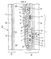
- a TFT array substrate 120 used in such a liquid crystal display device is, as shown in Fig. 15, formed, for example, by stacking, on a substrate 101, a protective underlayer 102 made of a silicon oxide film (SiO 2 film) or the like, a switching element made of a thin-film transistor (TFT) 103 or the like, a gate insulating film 103a, a source line 104, an interlayer insulating film 105, a protective film 105a made of a silicon nitride film (the protective film 105a is sometimes not formed), two layers made of organic photosensitive resin, such as acrylic resin, for forming surface irregularities for reflection under a transparent electrode 108, which will be described later, that is, a surface-irregularities forming layer 106 and an uneven layer 107, a transparent electrode 108 made of an ITO (Indium Tin Oxide) film, and a reflective plate 109 made of a single film of aluminum, silver, or an alloy thereof, or a composite film composed
- the source line 104 and the transparent electrode 108 are electrically connected by a contact hole 110 formed through the uneven layer 107.
- a transparent electrode 132 made of an ITO (Indium Tin Oxide) film is formed on a substrate 131.
- Alignment films 111 and 133 are formed on the surfaces of the TFT array substrate 120 and the counter ⁇ substrate 130 in which they face liquid crystal 50.
- the liquid crystal display device having such a configuration, however, since a voltage applied to the liquid crystal 50 between the transparent electrode 132 and the reflective plate 109 via the transparent electrode 108 drops at the reflective plate 109, the effective voltage also drops, and therefore, the display contrast decreases. Moreover, since the reflective plate 109 is exposed in a bare state at the side opposing the liquid crystal, the metal film forming the reflective plate 109 is prone to deterioration.
- the present invention has been made in view of the above problems, and an object of the present invention is to provide an electrooptic device which is suitable for use in a portable telephone, a mobile computer, and the like, and in which the effective voltage to be applied to the liquid crystal is high, high-contrast display is possible, and a reflective electrode is prevented from deteriorating, and to provide a production method for the electrooptic device.
- an electrooptic device of the present invention includes a pair of substrates opposing each other so as to seal and hold an electrooptic substance therebetween, and a reflective plate formed on the side of one of the pair of substrates close to the electrooptic substance, and having one or more openings, each at a predetermined position, for reflecting incident light from the other one of the substrates, and for transmitting light from a backlight source, wherein a transparent electrode is formed on the reflective plate and is electrically connected to a drain electrode or a semiconductor layer.
- Such a configuration makes it possible to increase the effective voltage to be applied to the liquid crystal in order to produce a higher-contrast display, and to prevent the reflective plate from deteriorating.
- the electrooptic device of the present invention may include a pair of substrates opposing each other so as to seal and hold an electrooptic substance therebetween, and a reflective plate formed on the side of one of the pair of substrates close to the electrooptic substance, and having one or more openings, each at a predetermined position, for reflecting incident light from the other one of the substrates, and for transmitting light from a backlight source, wherein a transparent electrode is formed on the reflective plate, and said reflective plate is a reflective electrode electrically connected to a drain electrode or a semiconductor layer.
- Such a configuration can prevent the reflective plate from deteriorating.
- the reflective plate is made of a single film of aluminum, silver, or an alloy containing at least one of aluminum and silver, or a composite film composed of the metal or alloy, and titanium, titanium nitride, molybdenum, tantalum, or the like.
- the transparent electrode is made of an ITO (Indium Tin Oxide) film.
- the transparent electrode is made of an ITO (Indium Tin Oxide) film.
- the area in which the transparent electrode is formed is wider than the area in which the reflective plate is formed.
- the electrooptic device further includes an uneven layer formed under the reflective plate and the transparent electrode, and having surface irregularities, and the reflective plate has an uneven surface that conforms to the irregularities of the uneven layer so as to scatter reflected light.
- An electrooptic device production method of the present invention includes the steps of forming a reflective plate on the side of one of a pair of substrates opposing each other so as to seal and hold an electrooptic substance therebetween, the side being close to the electrooptic substance, forming one or more openings, each at a predetermined position in the reflective plate, for reflecting incident light from the other one of the pair of substrates and for transmitting light from a backlight source, forming a transparent electrode on the reflective plate so as to cover an area of the reflective plate corresponding to the openings, and electrically connecting the transparent electrode to a drain electrode or a semiconductor layer.
- the electrooptic device production method of the present invention includes the steps of forming a reflective plate on a side of one of a pair of substrates opposing each other so as to seal and hold an electrooptic substance therebetween, the side being close to the electrooptic substance, forming one or more openings, each at a predetermined position in the reflective plate, for reflecting incident light from the other one of the pair of substrates and for transmitting light from a backlight source, electrically connecting the reflective plate to a drain electrode or a semiconductor layer so as to form a reflective electrode, and forming a transparent electrode on the reflective electrode so as to cover an area of the reflective electrode corresponding to the openings.
- a single film of aluminum, silver, or an alloy containing at least one of aluminum and silver, or a composite film composed of the metal or alloy, and titanium, titanium nitride, molybdenum, tantalum, or the like is used as the reflective electrode.
- an ITO (Indium Tin Oxide) film is used as the transparent electrode.
- the area in which the transparent electrode is formed is wider than the area in which the reflective electrode is formed in the step of forming the transparent electrode.
- the production method further includes a step of forming an uneven layer having surface irregularities on the one substrate before the step of forming the reflective electrode.
- Fig. 1 is plan view of a liquid crystal display device with components as an electrooptic device according to an embodiment of the present invention, as viewed from the side of a counter substrate, and Fig. 2 is a sectional view, taken along line H-H' in Fig. 1.
- Fig. 3 is an equivalent circuit diagram showing elements, lines, and the like in a plurality of pixels formed in a matrix in an image display region of the electrooptic device (liquid crystal display device).
- layers and members are shown on different scales in order that they have sizes viewable in the drawings.
- a TFT array substrate 10 (first substrate) and a counter substrate 20 (second substrate) are bonded with a sealing material 52, and liquid crystal 50 serving as an electrooptic substance is sealed and held in a region defined by the sealing material 52 (liquid-crystal sealed region).
- a light-shielding layer 53 for enclosing an image display region is made of a light-shielding material inside an area in which the sealing material 52 is formed.
- a data-line driving circuit 201 and leads 202 are formed along one side of the TFT array substrate 10 outside the sealing material 52, and scanning-line driving circuits 204 are formed along two sides next to the side.
- a plurality of wires 205 for connecting the scanning-line driving circuits 204 disposed on both sides of the image display region are formed on the remaining side of the TFT array substrate 10, and a precharge circuit and a detection circuit are sometimes formed, for example, under the light-shielding layer 53.
- a conductive material 206 is placed at at least one corner of the counter substrate 20 so as to electrically connect the TFT array substrate 10 and the counter substrate 20.
- a TAB (tape automated bonding) substrate on which a driving LSI is mounted, and a group of terminals formed on the periphery of the TFT array substrate 10 may be electrically and mechanically connected by an anisotropic conductive film.
- a polarizing film, a retardation film, a polarizer, and the like are placed in predetermined orientations in the electrooptic device 100, depending on the type of the liquid crystal 50 to be used, that is, depending on the driving mode such as a TN (twisted nematic) mode or an STN (super TN) mode, and a normally white mode/a normally black mode, they are not shown.
- red (R), green (G), and blue (B) color filters and protective films therefor are formed in regions of the counter substrate 20 opposing pixel electrodes of the TFT array substrate 10 which will be described later.
- a plurality of pixels 100a are arranged in a matrix, the pixels 100a are provided with TFTs 30 for pixel switching, respectively, and data lines 6a for supplying pixel signals S1, S2, ..., and Sn are electrically connected to sources of the corresponding TFTs 30.
- the pixel signals S1, S2, ..., and Sn to be written in the data lines 6a may be supplied in that order in a line-sequential manner (in the order of line number), and every group of the pixel signals may be supplied to a plurality of adjoining data lines 6a.
- Scanning lines 3a are electrically connected to gates of the corresponding TFTs 30 so that scan signals G1, G2, ..., and Gm are applied to the scanning lines 3a in that order in a line-sequential manner (in the order of line number) at a predetermined timing and in a pulsed form.
- Reflective electrodes 8 and transparent electrodes 9 are electrically connected to drains of the corresponding TFTs 30, and the pixel signals S1, S2, ..., and Sn supplied from the data lines 6a are written in the corresponding pixels at a predetermined timing by activating the TFTs 30 serving as the switching elements for a predetermined period.
- the pixel signals S1, S2, ..., and Sn at a predetermined level that are thus written in the liquid crystal via the reflective electrodes 8 and the transparent electrodes 9 are held between the reflective electrode 8 and the transparent electrode 9, and counter electrodes 21 of the counter substrate 20 shown in Fig. 2 for a predetermined period.
- the orientation and order of an aggregation of molecules change depending on the level of a voltage applied thereto, thereby modulating light and enabling grayscale display.
- the amount of incident light passing through the liquid crystal 50 decreases depending on the applied voltage in a normally white mode, and the amount of incident light passing through the liquid crystal 50 increases depending on the applied voltage in a normally black mode.
- light having a contrast in accordance with the pixel signals S1, S2, ..., and Sn is emitted from the electrooptic device 100 as a whole.
- storage capacitors 60 are sometimes added in parallel with liquid crystal capacitance formed between the transparent electrodes (pixel electrodes) 9 and the counter electrodes 21.
- the voltage of the transparent electrode 9 is held in the storage capacitor 60 for a time three orders of magnitude longer than the time during which the source voltage is applied. This improves the charge retention characteristics, and allows the electrooptic device 100 to achieve a high contrast.
- the storage capacitor 60 may be formed between the data line 6a and a capacitor line 3b serving as a line for forming the storage capacitor 60, as shown in Fig. 3, or between the data line 6a and the above-described scanning lines 3a.
- Fig. 4 is a plan view of one pixel in the TFT array substrate 10 used in this embodiment.
- Fig. 5 is a sectional view of the pixel in the electrooptic device shown in Fig. 4, taken along line A-A' in Fig. 4.
- a transparent electrode 9 is formed on each of reflective plates 8 that are arranged in a matrix on the TFT array substrate 10 and are made of a single film of aluminum or an aluminum alloy, or a composite film composed of the metal or alloy, and titanium, titanium nitride, molybdenum, tantalum, or the like.
- the transparent electrode 9 is electrically connected to a drain electrode 6b of a TFT 30 for pixel switching.
- a data line 6a, a scanning line 3a, and a capacitor line 3b are formed along the lengthwise and breadthwise boundaries between the areas in which the reflective plates 8 are formed, and the TFT 30 is connected to the data line 6a and the scanning line 3a.
- the data line 6a is electrically connected to a heavily doped source region 1a of a semiconductor film 1 of the TFT 30 via a contact hole, and the transparent electrode 9 is electrically connected to a heavily doped drain region 1d of the semiconductor film 1 of the TFT 30.
- an area in which an opening 14 is formed, of a region in which the reflective plate 8 is formed serves as a transmissive area covered with the transparent electrode 9 and used to perform image display in a transmissive mode, and the other area serves as a reflective area having the reflective plate 8 and used to perform image display in a reflective mode.
- a protective underlayer 11 made of a silicon oxide film (insulating film) of 300 nm to 500 nm in thickness is formed on the surface of a transparent substrate 10' serving as a base of the TFT array substrate 10, and an island-shaped semiconductor film 1 of 30 nm to 100 nm in thickness is formed on the surface of the protective underlayer 11.
- a gate insulating film 2 made of a silicon oxide film having a thickness of approximately 50 nm to 150 nm is formed on the surface of the semiconductor film 1, and a scanning line 3a of 300 nm to 800 nm in thickness extends as a gate electrode on the surface of the gate insulating film 2.
- An area of the semiconductor film 1 opposing the scanning line 3a with the gate insulating film 2 therebetween serves as a channel-forming region 1a'.
- a source region including a lightly doped region 1b and the heavily doped source region 1a is formed on one side of the channel-forming region 1a', and a drain region including a lightly doped region 1b and the heavily doped drain region 1d is formed on the other side.
- Reference numeral 1c in the figure denotes a heavily doped region.
- a first interlayer insulating film 4 made of a silicon oxide film having a thickness of 300 nm to 800 nm is formed on the front side of the TFT 30 for pixel switching.
- the data line 6a of 300 nm to 800 nm in thickness is formed on the surface of the first interlayer insulating film 4, and is electrically connected to the heavily doped source region 1a via a contact hole formed in the first interlayer insulating film 4.
- a drain electrode 6b is formed simultaneously with the data line 6a on the surface of the first interlayer insulating film 4, and is electrically connected to the heavily doped drain region 1d via a contact hole formed in the first interlayer insulating film 4.
- a second interlayer insulating film (surface-protecting film) 5 is formed of, for example, a single silicon nitride film or silicon oxide film, or two films composed of a silicon nitride film and a silicon oxide film on the first interlayer insulating film 4 (the second interlayer insulating film (surface-protecting film) 5 may be omitted).
- a surface-irregularities forming layer 13 and an uneven layer 7 made of a photosensitive resin, such as organic resin, are formed in that order on the second interlayer insulating film (surface-protecting film) 5, and a reflective plate 8 made of an aluminum film or the like having a transmission opening 14 is formed on the surface of the uneven layer 7.
- An uneven pattern 8g which conforms to the uneven surface of the uneven layer 7 is formed on the surface of the reflective plate 8.
- a transparent electrode 9 of approximately 50 nm to 200 nm in thickness is formed of a stack of ITO films on the reflective plate 8, and is electrically connected to the drain electrode 6b via a contact hole 15.
- An alignment film 12 is formed of a polyimide film on the front side of the transparent electrode 9.
- the alignment film 12 is subjected to rubbing.
- a capacitor line 3b which is formed in the same layer as the scanning line 3a opposes, as an upper electrode, an extended portion 1f (lower electrode) extending from the heavily doped drain region 1d with an insulating film (dielectric film), which is formed simultaneously with the gate insulating film 2, therebetween, thereby constituting a storage capacitor 60.
- the TFT 30 may have an offset structure in which impurity ions are not implanted in the regions corresponding to the lightly doped source region 1b and the lightly doped drain region 1c.
- the TFT 30 may be of a self-aligned type in which high-concentration impurity ions are implanted by using the gate electrode (part of the scanning line 3a) as a mask, and heavily doped source and drain regions are formed in a self-aligned manner.
- this embodiment adopts a dual gate (double gate) structure in which two gate electrodes (scanning line 3a) of the TFT 30 are placed in the source-drain region
- it may adopt a single gate structure having one gate electrode, a triple gate structure, or a structure in which more than three gate electrodes are placed.
- the same signal is applied to each gate electrode.
- the uneven pattern 8g is formed in a region on the surface of the reflective plate 8 outside the region where the TFT 30 and the opening 14 are formed in the reflection region of each pixel 100a of the TFT array substrate 10 (reflective electrode forming region), as described above.
- the surface-irregularities forming layer 13 made of an organic photosensitive resin, such as acrylic resin, and having a thickness of 1 ⁇ m to 3 ⁇ m is formed, for example, by spin coating, on the surface of the second interlayer insulating film 5 in a region that two-dimensionally overlaps with the reflective plate 8 on the lower side of the reflective plate 8, and the uneven layer 7 of 1 ⁇ m to 2 ⁇ m in thickness is formed of an insulating film made of a fluid, such as an organic photosensitive resin, for example, acrylic resin, on the surface-irregularities forming layer 13, for example, by spin coating.
- a fluid such as an organic photosensitive resin, for example, acrylic resin
- the surface-irregularities forming layer 13 has multiple irregularities. For this reason, as shown in Fig. 5, the uneven pattern 8g is formed on the surface of the reflective plate 8 so as to conform to the uneven surface of the uneven layer 7, and the edges of the surface-irregularities forming layer 13 are prevented by the uneven layer 7 from being exposed at the uneven pattern 8g.
- the edges of the irregularities of the surface-irregularities forming layer 13 may be smoothened by forming the surface-irregularities forming layer 13 and then performing baking without forming the uneven layer 7.
- a light-shielding film 23 which is called a black matrix or a black stripe, is formed in regions of the counter substrate 20 opposing the lengthwise and breadthwise boundaries of the transparent electrodes 9 formed in the TFT array substrate 10, and a counter electrode 21 is formed of an ITO film thereon.
- An alignment film 22 is formed of a polyimide film on the counter electrode 21. Liquid crystal 50 is sealed and held between the TFT array substrate 10 and the counter substrate 20.
- the reflective electrodes 8 are formed of an aluminum film or the like in the electrooptic device 100 having such a configuration (see Fig. 1), light incident from the side of the counter substrate 20 can be reflected by the TFT array substrate 10 and can be emitted from the counter substrate 20. Therefore, a predetermined image can be displayed with external light by performing optical modulation with the liquid crystal 50 in every pixel 100a during this process (reflection mode).
- the electrooptic device 100 can also function as a transmissive liquid crystal display device.
- the surface-irregularities forming layer 13 is formed on the lower side of the reflective plate 8 so as to two-dimensionally overlap with the reflective plate 8, and the uneven pattern 8g for light scattering is formed on the surface of the reflective plate 8 by using the irregularities of the surface-irregularities forming layer 13.
- the edges of the surface-irregularities forming layer 13 or the like are prevented by the uneven layer 7 from being exposed in the uneven pattern 8g. Therefore, when an image is displayed with scattered and reflected light in the reflection mode, the dependency on the angle of view is low.
- the reflective plate 8 Since the surface of the reflective plate 8 is covered with the transparent electrode 9, the reflective plate 8 can be prevented from deteriorating.
- the transparent electrode and the drain electrode are electrically connected in this embodiment, the transparent electrode and the semiconductor layer may be electrically connected.
- Fig. 6 is a sectional view schematically showing a liquid crystal display device as an electrooptic device according to another embodiment of the present invention.
- the liquid crystal display device shown in Fig. 6 is different from the liquid crystal display device shown in Fig. 5 in that a drain electrode 6b is not electrically connected to a transparent electrode 9, but is electrically connected to a reflective electrode 8'. Since the surface of the reflective electrode 8' is also covered with the transparent electrode 9 in this case, the reflective electrode 8' can be prevented from deteriorating.
- the reflective electrode and the drain electrode (source line) are also electrically connected in this embodiment, the reflective electrode and a semiconductor layer may be connected electrically.
- Figs. 7 to 11 are sectional views sequentially showing the processes of the method for producing the TFT array substrate of this embodiment.
- a substrate 10' made of glass or the like that is cleaned, for example, by ultrasonic cleaning is prepared, and a protective underlayer 11 made of a silicon oxide film and having a thickness of 100 nm to 500 nm is formed on the entire surface of the substrate 10' by plasma CVD under conditions where the substrate temperature is 150°C to 450°C.
- Material gases used in this case are, for example, a mixture of monosilane and laughing gas (nitrous oxide), a mixture of TEOS (tetraethoxysilane: Si(OC 2 H 5 ) 4 ) and oxygen, or a mixture of disilane and ammonium.
- a semiconductor film 1 made of an amorphous silicon film and having a thickness of 30 nm to 100 nm is formed on the entire surface of the substrate 10' by plasma CVD under conditions where the substrate temperature is 150°C to 450°C.
- the substrate temperature is 150°C to 450°C.
- disilane and monosilane may be used as material gases.
- the semiconductor film 1 is subjected to laser annealing by being irradiated with laser light. As a result, the amorphous semiconductor film 1 is melted, and is crystallized through cooling and solidification processes.
- the irradiation time of the regions irradiated with the laser light in this case is quite short, and the regions to be irradiated are local with respect to the entirety of the substrate, all the regions of the substrate will not be simultaneously heated to a high temperature. For this reason, even when a glass substrate or the like is used as the substrate 10', it will not be subjected to deformation, cracking, or the like due to heat.
- an island-shaped semiconductor film 1 (active layer) and a semiconductor film for forming a storage capacitance region are separately formed by etching the surface of the semiconductor film 1 by photolithography using resist masks 551, as shown in Fig. 7(B).
- a gate insulating film 2 made of a silicon oxide film or the like and having a thickness of 50 nm to 150 nm is formed on the entire surface of the substrate 10' and the surface of the semiconductor film 1, for example, by CVD at a temperature of 350°C or less.
- a mixture of TEOS and gaseous oxygen may be used as the material gas.
- the gate insulating film 2 used in this case may be a silicon nitride film, instead of the silicon oxide film.
- a lower electrode for forming a storage capacitor 60 between the semiconductor film 1 and a capacitor line 3b is formed by implanting impurity ions into an extended portion if of the semiconductor film 1 via a predetermined resist mask (see Figs. 4 and 5).
- resist masks 552 are formed by photolithography, as shown in Fig. 7(C).
- a scanning line 3a (gate electrodes), a capacitor line 3b, and the like are formed by subjecting the conductive film 3 to dry etching using the resist masks 552, as shown in Fig. 7(D).
- a lightly doped region 1b is formed in a self-aligned fashion in relation to the scanning line 3a in a pixel TFT portion and an N-channel TFT portion (not shown) of a driving circuit by implanting impurity ions (phosphorus ions) at a dosage of approximately 0.1 ⁇ 10 13 /cm 2 to approximately 10 ⁇ 10 13 /cm 2 with the scanning line 3a and the gate electrodes used as masks.
- impurity ions phosphorus ions
- resist masks 553 wider than the scanning line 3a are formed in the pixel TFT portion, and high-concentration impurity ions (phosphorus ions) are implanted therein at a dosage of approximately 0.1 ⁇ 10 15 /cm 2 to approximately 10 ⁇ 10 15 /cm 2 , thereby forming a heavily doped source region 1a and a heavily doped drain region 1d.
- a source region and a drain region of an offset structure may be formed by implanting high-concentration impurities (phosphorus ions) while forming resist masks wider than the gate electrodes, without implanting low-concentration impurities.
- a source region and a drain region of a self-aligned structure may be formed by implanting high-concentration impurities with the scanning line 3a used as a mask.
- the N-channel TFT portion of a peripheral driving circuit is formed by such processes, and a P-channel TFT portion is covered with a mask in this case, although this is not shown.
- the pixel section and the N-channel TFT portion are covered with a resist for protection, and boron ions are implanted at a dosage of approximately 0.1 ⁇ 10 15 /cm 2 to approximately 10 ⁇ 10 15 /cm 2 with the gate electrodes used as masks, thereby forming a P-channel source-drain region in a self-aligned fashion.
- a source region and a drain region of an LDD structure may be used by forming a lightly doped region in a polysilicon film by the implantation of low-concentration impurities (boron ions) at a dosage of approximately 0.1 ⁇ 10 13 /cm 2 to approximately 10 ⁇ 10 13 /cm 2 with the gate electrodes as masks, in a manner similar to that in the formation of the N-channel TFT portion, and then implanting high-concentration impurities (boron ions) at a dosage of approximately 0.1 ⁇ 10 15 /cm 2 to approximately 10 ⁇ 10 15 /cm 2 using masks wider than the gate electrodes.
- low-concentration impurities boron ions
- a source region and a drain region of an offset structure may be formed by implanting high-concentration impurities (boron ions) using masks wider than the gate electrodes formed, without implanting low-concentration impurities. These ion implantation processes enable CMOS (Complimentary MOS), and allow the peripheral driving circuits to be incorporated on the same substrate.
- CMOS Complementary MOS
- a first interlayer insulating film 4 made of a silicon oxide film or the like and having a thickness of 300 nm to 800 nm is formed on the front side of the scanning line 3a, for example, by CVD.
- a mixture of TEOS and gaseous oxygen may be used as the material gas.
- a resist mask 554 is formed by photolithography.
- the first interlayer insulating film 4 is subjected to dry etching through the resist mask 554, and contact holes are thereby formed in portions of the first interlayer insulating film 4 corresponding to the source region and the drain region, as shown in Fig. 8(C).
- a conductive film 6 made of an aluminum film, a titanium film, a titanium nitride film, a tantalum film, a molybdenum film, or an alloy film chiefly containing any of these metals, and having a thickness of 300 nm to 800 nm is formed on the front side of the first interlayer insulating film 4, for example, by sputtering so as to form a data line 6a (source electrode) and the like, and a resist mask 555 is then formed by photolithography.
- a data line 6a and a drain electrode 6b are formed by subjecting the conductive film 6 to dry etching through the predetermined resist mask 555.
- a second interlayer insulating film (surface-protecting film) 5 made of a single film, such as a silicon nitride film or a silicon oxide film, or two films, that is, a silicon nitride film and a silicon oxide film, and having a thickness of approximately 100 nm to 300 nm is formed on the first interlayer insulating film 4 by CVD (the second interlayer insulating film 5 may be omitted).
- an organic photosensitive resin 13a such as acrylic resin
- having a thickness of 1 ⁇ m to 3 ⁇ m is applied on the surface of the second interlayer insulating film (surface-protecting film) 5 by spin coating, it is patterned by photolithography, thereby forming a surface-irregularities forming layer 13 of 1 ⁇ m to 3 ⁇ m in thickness under a reflective electrode 8, which will be described later.
- a baking process may be performed for smoothing.
- Fig. 10(A) shows a case in which the photosensitive resin 13a is of a positive type, and the portions of the photosensitive resin 13a to be removed are irradiated with ultraviolet rays through light-transmitting portions of a predetermined exposure mask.
- an organic photosensitive resin 7a such as acrylic resin, having a thickness of 1 ⁇ m to 2 ⁇ m is formed on the front sides of the second interlayer insulating film (surface-protecting film) 5 and the surface-irregularities forming layer 13 by spin coating.
- an uneven layer 7 of 1 ⁇ m to 2 ⁇ m is formed by photolithography so that a portion thereof is opened to reach the surface of the second interlayer insulating film (surface-protecting film) 5 (this portion finally forms a contact hole 15).
- the uneven layer 7 is formed by applying a fluid material, an edgeless and smooth uneven pattern is formed on the surface of the uneven layer 7 so as to moderately remove the irregularities of the surface-irregularities forming layer 13.
- the edges of the surface-irregularities forming layer 13 may be smoothened by performing a baking process in a state shown in Fig. 10(B).
- a contact hole 15 is formed by removing the second interlayer insulating film (surface-protecting film) 5 by dry etching using the uneven layer 7 as a mask so that a transparent electrode 9, which will be described later, and the drain electrode 6b can be electrically connected.
- a metal film 8a having a thickness of 50nm to 200 nm and a reflectivity like the above-described aluminum film or the like is formed, for example, by sputtering.
- a reflective plate 8 having an opening 14 is formed by selectively removing a portion between pixel portions next to the opening 14 by micromachining.
- an ITO film 9a of approximately 50 nm to 200 nm in thickness is formed, for example, by sputtering.
- a transparent electrode 9 having a predetermined pattern is formed by photolithography and etching.
- the transparent electrode 9 it is preferable that the transparent electrode 9 be formed over a wider area than the area in which the reflective plate 8 is formed.
- the transparent electrode 9 and the drain electrode 6b are electrically connected.
- An uneven pattern 8g having a thickness of 500 nm or more, or 800 nm or more is formed of the irregularities made by the surface-irregularities forming layer 13 and the uneven layer 7 on the surfaces of the reflective plate 8 and the transparent electrode 9 thus formed, and the uneven pattern 8g is made edgeless and smooth by the uneven layer 7.
- an alignment film (polyimide film) 12 is formed on the front side of the transparent substrate 9.
- a polyimide varnish in which 5 to 10 weight percent polyimide or polyimide acid is melted in a solvent such as butyl cellosolve or n-methylpyrrolidone is subjected to flexography, and is set (baked) by heating.
- the substrate with the polyimide film thereon is rubbed with a fabric puff made of rayon fibers in a fixed direction so that the polyimide molecules are aligned in a fixed direction adjacent to the surface (subjected to rubbing).
- a fabric puff made of rayon fibers in a fixed direction so that the polyimide molecules are aligned in a fixed direction adjacent to the surface (subjected to rubbing).
- liquid crystal molecules that will be injected later are aligned in a fixed direction by the interaction between the liquid crystal molecules and the polyimide molecules.
- the TFT array substrate 10 is completed through the above-described procedure.
- liquid crystal display devices of the above embodiments are of an active matrix type using a TFT as the pixel switching element
- the present invention may be applied to an active matrix liquid crystal display device using a TFD as the pixel switching element, a passive matrix liquid crystal display device, or an electrooptic device using an electrooptic substance other than the liquid crystal (for example, an EL light-emitting element).
- the semi-reflective and semi-transmissive electrooptic device 100 having such a configuration may be used as a display section for various electronic devices, an example thereof will be specifically described with reference to Figs. 12 to 14.
- Fig. 12 is a block diagram showing the circuit configuration of an electronic device that uses the electrooptic device of the present invention as a display device.
- the electronic device includes a display information output source 70, a display information processing circuit 71, a power supply circuit 72, a timing generator 73, and a liquid crystal display device 74.
- the liquid crystal display device 74 has a liquid crystal display panel 75 and a driving circuit 76.
- the above-described electrooptic device 100 may be used as the liquid crystal device 74.
- the display information output source 70 includes a memory, such as a ROM (Read Only Memory) or a RAM (Random Access Memory), a storage unit, such as various disks, a tuned circuit for outputting digital image signals in a tuned manner, and the like, and supplies display information, such as a predetermined-format image signal, to the display information processing circuit 71 according to various clock signals generated by the timing generator 73.
- a memory such as a ROM (Read Only Memory) or a RAM (Random Access Memory)
- a storage unit such as various disks
- a tuned circuit for outputting digital image signals in a tuned manner and the like
- the display information processing circuit 71 includes various known circuits, such as a serial-parallel conversion circuit, amplifying and inverting circuits, a rotation circuit, a gamma correction circuit, and a clamp circuit, processes input display information, and supplies an image signal corresponding thereto to the driving circuit 76 with a clock signal CLK.
- the power supply circuit 72 supplies a predetermined voltage to each component.
- FIG. 13 shows a mobile personal computer as an electronic device according to an example of the present invention.
- a personal computer 80 shown herein includes a body section 82 having a keyboard 81, and a liquid crystal display unit 83.
- the liquid crystal display unit 83 includes the above-described electrooptic device 100.
- Fig. 14 shows a portable telephone as another electronic device.
- a portable telephone 90 shown herein includes a plurality of control buttons 91, and a display section formed of the above-described electrooptic device 100.
- the present invention can provide an electrooptic device which is suitable for use in a portable telephone, a mobile computer, and the like, and in which the effective voltage to be applied to the liquid crystal is high, high-contrast display is possible, and a reflective electrode is prevented from deteriorating, and can provide a production method for the electrooptic device.
Abstract
Description
- The present invention relates to an electrooptic device and a production method therefor. More particularly, the present invention relates to an electrooptic device which is suitable for use in a portable telephone, a mobile computer, and the like, and in which the effective voltage to be applied to liquid crystal is high, high-contrast display is possible, and a reflective electrode and a reflective plate are prevented from deteriorating, and relates to a production method for the electrooptic device.
- Electrooptic devices (for example, liquid crystal display devices and EL light-emitting display devices) are widely used as direct-view display devices in various electronic devices such as portable telephones and mobile computers. For example, in an active matrix semi-transmissive and semi-reflective liquid crystal display device of such electrooptic devices, a TFT array substrate and a counter substrate opposing each other are bonded with a sealing material, and liquid crystal serving as an electrooptic substance is sealed and held between the substrates in a region defined by the sealing material.
- A reflective plate is formed on the surface of the TFT array substrate so as to reflect external light incident from the counter substrate side back toward the counter substrate, light incident from the counter substrate is reflected by the reflective plate of the TFT array substrate, and an image is displayed with the light emitted from the counter substrate (reflection mode). The reflective plate has an opening for transmitting light, a transparent electrode is formed under the reflective plate so as to cover the opening, and an image is displayed with light from a backlight passing through the opening (transmissive mode).
- A
TFT array substrate 120 used in such a liquid crystal display device is, as shown in Fig. 15, formed, for example, by stacking, on asubstrate 101, aprotective underlayer 102 made of a silicon oxide film (SiO2 film) or the like, a switching element made of a thin-film transistor (TFT) 103 or the like, agate insulating film 103a, asource line 104, aninterlayer insulating film 105, aprotective film 105a made of a silicon nitride film (theprotective film 105a is sometimes not formed), two layers made of organic photosensitive resin, such as acrylic resin, for forming surface irregularities for reflection under atransparent electrode 108, which will be described later, that is, a surface-irregularities forming layer 106 and anuneven layer 107, atransparent electrode 108 made of an ITO (Indium Tin Oxide) film, and areflective plate 109 made of a single film of aluminum, silver, or an alloy thereof, or a composite film composed of the metal or alloy, and titanium, titanium nitride, molybdenum, or tantalum. Thesource line 104 and thetransparent electrode 108 are electrically connected by acontact hole 110 formed through theuneven layer 107. On the other hand, in acounter substrate 130, atransparent electrode 132 made of an ITO (Indium Tin Oxide) film is formed on asubstrate 131.Alignment films TFT array substrate 120 and the counter·substrate 130 in which they faceliquid crystal 50. - In the liquid crystal display device having such a configuration, however, since a voltage applied to the
liquid crystal 50 between thetransparent electrode 132 and thereflective plate 109 via thetransparent electrode 108 drops at thereflective plate 109, the effective voltage also drops, and therefore, the display contrast decreases. Moreover, since thereflective plate 109 is exposed in a bare state at the side opposing the liquid crystal, the metal film forming thereflective plate 109 is prone to deterioration. - The present invention has been made in view of the above problems, and an object of the present invention is to provide an electrooptic device which is suitable for use in a portable telephone, a mobile computer, and the like, and in which the effective voltage to be applied to the liquid crystal is high, high-contrast display is possible, and a reflective electrode is prevented from deteriorating, and to provide a production method for the electrooptic device.
- In order to achieve the above object, an electrooptic device of the present invention includes a pair of substrates opposing each other so as to seal and hold an electrooptic substance therebetween, and a reflective plate formed on the side of one of the pair of substrates close to the electrooptic substance, and having one or more openings, each at a predetermined position, for reflecting incident light from the other one of the substrates, and for transmitting light from a backlight source, wherein a transparent electrode is formed on the reflective plate and is electrically connected to a drain electrode or a semiconductor layer.
- Such a configuration makes it possible to increase the effective voltage to be applied to the liquid crystal in order to produce a higher-contrast display, and to prevent the reflective plate from deteriorating.
- The electrooptic device of the present invention may include a pair of substrates opposing each other so as to seal and hold an electrooptic substance therebetween, and a reflective plate formed on the side of one of the pair of substrates close to the electrooptic substance, and having one or more openings, each at a predetermined position, for reflecting incident light from the other one of the substrates, and for transmitting light from a backlight source, wherein a transparent electrode is formed on the reflective plate, and said reflective plate is a reflective electrode electrically connected to a drain electrode or a semiconductor layer.
- Such a configuration can prevent the reflective plate from deteriorating.
- In this case, preferably, the reflective plate is made of a single film of aluminum, silver, or an alloy containing at least one of aluminum and silver, or a composite film composed of the metal or alloy, and titanium, titanium nitride, molybdenum, tantalum, or the like. Furthermore, preferably, the transparent electrode is made of an ITO (Indium Tin Oxide) film.
- This can increase the light reflection efficiency.
- Preferably, the transparent electrode is made of an ITO (Indium Tin Oxide) film.
- This can increase the display contrast in a transmissive mode.
- Preferably, the area in which the transparent electrode is formed is wider than the area in which the reflective plate is formed.
- This can prevent the reflective plate from deteriorating.
- Preferably, the electrooptic device further includes an uneven layer formed under the reflective plate and the transparent electrode, and having surface irregularities, and the reflective plate has an uneven surface that conforms to the irregularities of the uneven layer so as to scatter reflected light.
- This can improve the reflection characteristics.
- An electrooptic device production method of the present invention includes the steps of forming a reflective plate on the side of one of a pair of substrates opposing each other so as to seal and hold an electrooptic substance therebetween, the side being close to the electrooptic substance, forming one or more openings, each at a predetermined position in the reflective plate, for reflecting incident light from the other one of the pair of substrates and for transmitting light from a backlight source, forming a transparent electrode on the reflective plate so as to cover an area of the reflective plate corresponding to the openings, and electrically connecting the transparent electrode to a drain electrode or a semiconductor layer.
- This makes it possible to efficiently and cheaply produce an electrooptic device in which the effective voltage to be applied to the liquid crystal is high, high-contrast display is possible, and deterioration of the reflective plate is prevented.
- The electrooptic device production method of the present invention includes the steps of forming a reflective plate on a side of one of a pair of substrates opposing each other so as to seal and hold an electrooptic substance therebetween, the side being close to the electrooptic substance, forming one or more openings, each at a predetermined position in the reflective plate, for reflecting incident light from the other one of the pair of substrates and for transmitting light from a backlight source, electrically connecting the reflective plate to a drain electrode or a semiconductor layer so as to form a reflective electrode, and forming a transparent electrode on the reflective electrode so as to cover an area of the reflective electrode corresponding to the openings.
- This makes it possible to efficiently and cheaply produce an electrooptic device in which deterioration of the reflective electrode is prevented.
- In this case, preferably, a single film of aluminum, silver, or an alloy containing at least one of aluminum and silver, or a composite film composed of the metal or alloy, and titanium, titanium nitride, molybdenum, tantalum, or the like is used as the reflective electrode.
- This makes it possible to efficiently and cheaply produce an electrooptic device having an increased light reflection efficiency.
- Preferably, an ITO (Indium Tin Oxide) film is used as the transparent electrode.
- This makes it possible to efficiently and cheaply produce an electrooptic device having an increased display contrast in a transmissive mode.
- Preferably, the area in which the transparent electrode is formed is wider than the area in which the reflective electrode is formed in the step of forming the transparent electrode.
- This makes it possible to efficiently and cheaply produce an electrooptic device, in which deterioration of the reflective electrode is prevented.
- Preferably, the production method further includes a step of forming an uneven layer having surface irregularities on the one substrate before the step of forming the reflective electrode.
- This makes it possible to efficiently and cheaply produce an electrooptic device having an improved reflection characteristic.
- Embodiments of the present invention will now be described by way of further example only and with reference to the accompanying drawings, in which:-
- Fig. 1 is a plan view of an electrooptic device according to an embodiment of the present invention, as viewed from the side of a counter substrate.
- Fig. 2 is a sectional view, taken along line H-H' in Fig. 1.
- Fig. 3 is an equivalent circuit diagram showing elements, lines, and the like formed in a plurality of pixels arranged in a matrix in the electrooptic device according to the embodiment of the present invention.
- Fig. 4 is a plan view showing the structure of each pixel formed in a TFT array substrate in the electrooptic device according to the embodiment of the present invention.
- Fig. 5 is a sectional view of the pixel, taken along line A-A' in Fig. 4.
- Fig. 6 is a sectional view showing the structure of each pixel formed in a TFT array substrate in an electrooptic device according to another embodiment of the present invention.
- Figs. 7(A) to 7(D) are sectional views sequentially showing the processes for producing a TFT array substrate in an electrooptic device production method according to an embodiment of the present invention.
- Figs. 8(A) to 8(D) are sectional views sequentially showing the processes for producing the TFT array substrate subsequent to the processes shown in Figs. 7(A) to 7(D).
- Figs. 9(A) and 9(B) are sectional views sequentially showing the processes for producing the TFT array substrate subsequent to the processes shown in Figs. 8(A) to 8(D).
- Figs. 10(A) to 10(D) are sectional views sequentially showing the processes for producing the TFT array substrate subsequent to the processes shown in Figs. 9(A) and 9(B).
- Figs. 11(A) to 11(E) are sectional views sequentially showing the processes for producing the TFT array substrate subsequent to the processes shown in Figs. 10(A) to 10(D).
- Fig. 12 is a block diagram showing the circuit configuration of an electronic device using the electrooptic device of the present invention as a display device.
- Fig. 13 is an explanatory view of a mobile personal computer as an example of an electronic device using the electrooptic device of the present invention.
- Fig. 14 is an explanatory view of a portable telephone as an example of an electronic device using the electrooptic device of the present invention.
- Fig. 15 is a sectional view schematically showing a part of a pixel in a conventional electrooptic device.
-
- An electrooptic device and a production method therefor according to an embodiment of the present invention will be specifically described below with reference to the drawings.
- Fig. 1 is plan view of a liquid crystal display device with components as an electrooptic device according to an embodiment of the present invention, as viewed from the side of a counter substrate, and Fig. 2 is a sectional view, taken along line H-H' in Fig. 1. Fig. 3 is an equivalent circuit diagram showing elements, lines, and the like in a plurality of pixels formed in a matrix in an image display region of the electrooptic device (liquid crystal display device). In the drawings used to describe this embodiment, layers and members are shown on different scales in order that they have sizes viewable in the drawings.
- In Figs. 1 and 2, in an electrooptic device (liquid crystal display device) 100 of this embodiment, a TFT array substrate 10 (first substrate) and a counter substrate 20 (second substrate) are bonded with a sealing
material 52, andliquid crystal 50 serving as an electrooptic substance is sealed and held in a region defined by the sealing material 52 (liquid-crystal sealed region). A light-shielding layer 53 for enclosing an image display region is made of a light-shielding material inside an area in which the sealingmaterial 52 is formed. A data-line driving circuit 201 andleads 202 are formed along one side of theTFT array substrate 10 outside the sealingmaterial 52, and scanning-line driving circuits 204 are formed along two sides next to the side. A plurality ofwires 205 for connecting the scanning-line driving circuits 204 disposed on both sides of the image display region are formed on the remaining side of theTFT array substrate 10, and a precharge circuit and a detection circuit are sometimes formed, for example, under the light-shielding layer 53. Aconductive material 206 is placed at at least one corner of thecounter substrate 20 so as to electrically connect theTFT array substrate 10 and thecounter substrate 20. - Instead of forming the data-
line driving circuit 201 and the scanningline driving circuits 204 on theTFT array substrate 10, for example, a TAB (tape automated bonding) substrate on which a driving LSI is mounted, and a group of terminals formed on the periphery of theTFT array substrate 10 may be electrically and mechanically connected by an anisotropic conductive film. While a polarizing film, a retardation film, a polarizer, and the like are placed in predetermined orientations in theelectrooptic device 100, depending on the type of theliquid crystal 50 to be used, that is, depending on the driving mode such as a TN (twisted nematic) mode or an STN (super TN) mode, and a normally white mode/a normally black mode, they are not shown. - When the
electrooptic device 100 is adapted to color display, for example, red (R), green (G), and blue (B) color filters and protective films therefor are formed in regions of thecounter substrate 20 opposing pixel electrodes of theTFT array substrate 10 which will be described later. - In the image display region of the
electrooptic device 100 having such a configuration, as shown in Fig. 3, a plurality ofpixels 100a are arranged in a matrix, thepixels 100a are provided withTFTs 30 for pixel switching, respectively, anddata lines 6a for supplying pixel signals S1, S2, ..., and Sn are electrically connected to sources of the correspondingTFTs 30. The pixel signals S1, S2, ..., and Sn to be written in thedata lines 6a may be supplied in that order in a line-sequential manner (in the order of line number), and every group of the pixel signals may be supplied to a plurality of adjoiningdata lines 6a.Scanning lines 3a are electrically connected to gates of the correspondingTFTs 30 so that scan signals G1, G2, ..., and Gm are applied to thescanning lines 3a in that order in a line-sequential manner (in the order of line number) at a predetermined timing and in a pulsed form.Reflective electrodes 8 andtransparent electrodes 9 are electrically connected to drains of the correspondingTFTs 30, and the pixel signals S1, S2, ..., and Sn supplied from thedata lines 6a are written in the corresponding pixels at a predetermined timing by activating theTFTs 30 serving as the switching elements for a predetermined period. The pixel signals S1, S2, ..., and Sn at a predetermined level that are thus written in the liquid crystal via thereflective electrodes 8 and thetransparent electrodes 9 are held between thereflective electrode 8 and thetransparent electrode 9, andcounter electrodes 21 of thecounter substrate 20 shown in Fig. 2 for a predetermined period. - In the
liquid crystal 50, the orientation and order of an aggregation of molecules change depending on the level of a voltage applied thereto, thereby modulating light and enabling grayscale display. The amount of incident light passing through theliquid crystal 50 decreases depending on the applied voltage in a normally white mode, and the amount of incident light passing through theliquid crystal 50 increases depending on the applied voltage in a normally black mode. As a result, light having a contrast in accordance with the pixel signals S1, S2, ..., and Sn is emitted from theelectrooptic device 100 as a whole. - In order to prevent the held pixel signals S1, S2, ..., and Sn from leaking, storage capacitors 60 (see Fig. 3) are sometimes added in parallel with liquid crystal capacitance formed between the transparent electrodes (pixel electrodes) 9 and the
counter electrodes 21. For example, the voltage of thetransparent electrode 9 is held in thestorage capacitor 60 for a time three orders of magnitude longer than the time during which the source voltage is applied. This improves the charge retention characteristics, and allows theelectrooptic device 100 to achieve a high contrast. Thestorage capacitor 60 may be formed between thedata line 6a and acapacitor line 3b serving as a line for forming thestorage capacitor 60, as shown in Fig. 3, or between thedata line 6a and the above-describedscanning lines 3a. - Fig. 4 is a plan view of one pixel in the
TFT array substrate 10 used in this embodiment. Fig. 5 is a sectional view of the pixel in the electrooptic device shown in Fig. 4, taken along line A-A' in Fig. 4. - In Fig. 4, a
transparent electrode 9 is formed on each ofreflective plates 8 that are arranged in a matrix on theTFT array substrate 10 and are made of a single film of aluminum or an aluminum alloy, or a composite film composed of the metal or alloy, and titanium, titanium nitride, molybdenum, tantalum, or the like. Thetransparent electrode 9 is electrically connected to adrain electrode 6b of aTFT 30 for pixel switching. Adata line 6a, ascanning line 3a, and acapacitor line 3b are formed along the lengthwise and breadthwise boundaries between the areas in which thereflective plates 8 are formed, and theTFT 30 is connected to thedata line 6a and thescanning line 3a. That is, thedata line 6a is electrically connected to a heavily doped source region 1a of asemiconductor film 1 of theTFT 30 via a contact hole, and thetransparent electrode 9 is electrically connected to a heavily dopeddrain region 1d of thesemiconductor film 1 of theTFT 30. - As shown in Fig. 4, in each
pixel 100a having such a structure, an area in which anopening 14 is formed, of a region in which thereflective plate 8 is formed, serves as a transmissive area covered with thetransparent electrode 9 and used to perform image display in a transmissive mode, and the other area serves as a reflective area having thereflective plate 8 and used to perform image display in a reflective mode. - In the cross section of the reflection area taken along line A-A' in Fig. 4, as shown in Fig. 5, a
protective underlayer 11 made of a silicon oxide film (insulating film) of 300 nm to 500 nm in thickness is formed on the surface of a transparent substrate 10' serving as a base of theTFT array substrate 10, and an island-shapedsemiconductor film 1 of 30 nm to 100 nm in thickness is formed on the surface of theprotective underlayer 11. Agate insulating film 2 made of a silicon oxide film having a thickness of approximately 50 nm to 150 nm is formed on the surface of thesemiconductor film 1, and ascanning line 3a of 300 nm to 800 nm in thickness extends as a gate electrode on the surface of thegate insulating film 2. An area of thesemiconductor film 1 opposing thescanning line 3a with thegate insulating film 2 therebetween serves as a channel-forming region 1a'. A source region including a lightly dopedregion 1b and the heavily doped source region 1a is formed on one side of the channel-forming region 1a', and a drain region including a lightly dopedregion 1b and the heavily dopeddrain region 1d is formed on the other side.Reference numeral 1c in the figure denotes a heavily doped region. - A first
interlayer insulating film 4 made of a silicon oxide film having a thickness of 300 nm to 800 nm is formed on the front side of theTFT 30 for pixel switching. Thedata line 6a of 300 nm to 800 nm in thickness is formed on the surface of the firstinterlayer insulating film 4, and is electrically connected to the heavily doped source region 1a via a contact hole formed in the firstinterlayer insulating film 4. Adrain electrode 6b is formed simultaneously with thedata line 6a on the surface of the firstinterlayer insulating film 4, and is electrically connected to the heavily dopeddrain region 1d via a contact hole formed in the firstinterlayer insulating film 4. - A second interlayer insulating film (surface-protecting film) 5 is formed of, for example, a single silicon nitride film or silicon oxide film, or two films composed of a silicon nitride film and a silicon oxide film on the first interlayer insulating film 4 (the second interlayer insulating film (surface-protecting film) 5 may be omitted). A surface-
irregularities forming layer 13 and anuneven layer 7 made of a photosensitive resin, such as organic resin, are formed in that order on the second interlayer insulating film (surface-protecting film) 5, and areflective plate 8 made of an aluminum film or the like having atransmission opening 14 is formed on the surface of theuneven layer 7. Anuneven pattern 8g which conforms to the uneven surface of theuneven layer 7 is formed on the surface of thereflective plate 8. - A
transparent electrode 9 of approximately 50 nm to 200 nm in thickness is formed of a stack of ITO films on thereflective plate 8, and is electrically connected to thedrain electrode 6b via acontact hole 15. - An
alignment film 12 is formed of a polyimide film on the front side of thetransparent electrode 9. Thealignment film 12 is subjected to rubbing. - A
capacitor line 3b which is formed in the same layer as thescanning line 3a opposes, as an upper electrode, an extended portion 1f (lower electrode) extending from the heavily dopeddrain region 1d with an insulating film (dielectric film), which is formed simultaneously with thegate insulating film 2, therebetween, thereby constituting astorage capacitor 60. - While it is preferable that the
TFT 30 have the above-described LDD structure, it may have an offset structure in which impurity ions are not implanted in the regions corresponding to the lightly dopedsource region 1b and the lightly dopeddrain region 1c. Alternatively, theTFT 30 may be of a self-aligned type in which high-concentration impurity ions are implanted by using the gate electrode (part of thescanning line 3a) as a mask, and heavily doped source and drain regions are formed in a self-aligned manner. - While this embodiment adopts a dual gate (double gate) structure in which two gate electrodes (scanning
line 3a) of theTFT 30 are placed in the source-drain region, it may adopt a single gate structure having one gate electrode, a triple gate structure, or a structure in which more than three gate electrodes are placed. When a plurality of gate electrodes are provided, the same signal is applied to each gate electrode. By thus providing theTFT 30 with the dual gate (double gate) structure, the triple gate structure, or the structure having more gates, a leakage current can be avoided at a joint portion between the channel and the source-drain region, and the current in an OFF state can be reduced. By providing at least one of the gate electrodes with an LDD structure or an offset structure, the OFF current can be further reduced, and this can achieve a stable switching element. - In Figs. 4 and 5, the
uneven pattern 8g is formed in a region on the surface of thereflective plate 8 outside the region where theTFT 30 and theopening 14 are formed in the reflection region of eachpixel 100a of the TFT array substrate 10 (reflective electrode forming region), as described above. - In order to form such an
uneven pattern 8g in theTFT array substrate 10 of this embodiment, the surface-irregularities forming layer 13 made of an organic photosensitive resin, such as acrylic resin, and having a thickness of 1 µm to 3 µm is formed, for example, by spin coating, on the surface of the secondinterlayer insulating film 5 in a region that two-dimensionally overlaps with thereflective plate 8 on the lower side of thereflective plate 8, and theuneven layer 7 of 1 µm to 2 µm in thickness is formed of an insulating film made of a fluid, such as an organic photosensitive resin, for example, acrylic resin, on the surface-irregularities forming layer 13, for example, by spin coating. - The surface-
irregularities forming layer 13 has multiple irregularities. For this reason, as shown in Fig. 5, theuneven pattern 8g is formed on the surface of thereflective plate 8 so as to conform to the uneven surface of theuneven layer 7, and the edges of the surface-irregularities forming layer 13 are prevented by theuneven layer 7 from being exposed at theuneven pattern 8g. The edges of the irregularities of the surface-irregularities forming layer 13 may be smoothened by forming the surface-irregularities forming layer 13 and then performing baking without forming theuneven layer 7. - In Fig. 5, a light-shielding
film 23, which is called a black matrix or a black stripe, is formed in regions of thecounter substrate 20 opposing the lengthwise and breadthwise boundaries of thetransparent electrodes 9 formed in theTFT array substrate 10, and acounter electrode 21 is formed of an ITO film thereon. Analignment film 22 is formed of a polyimide film on thecounter electrode 21.Liquid crystal 50 is sealed and held between theTFT array substrate 10 and thecounter substrate 20. - Since the
reflective electrodes 8 are formed of an aluminum film or the like in theelectrooptic device 100 having such a configuration (see Fig. 1), light incident from the side of thecounter substrate 20 can be reflected by theTFT array substrate 10 and can be emitted from thecounter substrate 20. Therefore, a predetermined image can be displayed with external light by performing optical modulation with theliquid crystal 50 in everypixel 100a during this process (reflection mode). - Since the
reflective electrodes 8 are formed so as not to touch theopenings 14 shown in Fig. 4, theelectrooptic device 100 can also function as a transmissive liquid crystal display device. - That is, light emitted from a backlight device (not shown) placed on the side of the
TFT array substrate 10 enters theTFT array substrate 10, and then travels toward thecounter substrate 20 after passing through the transmissive area that does not have the reflective electrode 8 (theopening 14 covered with the transparent electrode 9) in the region of eachpixel 100a (see Fig. 3) in which thereflective plate 8 is formed. For this reason, a predetermined image can be displayed with the light emitted from the backlight device by performing optical modulation with theliquid crystal 50 in everypixel 100a (transmission mode). - In this embodiment, the surface-
irregularities forming layer 13 is formed on the lower side of thereflective plate 8 so as to two-dimensionally overlap with thereflective plate 8, and theuneven pattern 8g for light scattering is formed on the surface of thereflective plate 8 by using the irregularities of the surface-irregularities forming layer 13. The edges of the surface-irregularities forming layer 13 or the like are prevented by theuneven layer 7 from being exposed in theuneven pattern 8g. Therefore, when an image is displayed with scattered and reflected light in the reflection mode, the dependency on the angle of view is low. - Since the surface of the
reflective plate 8 is covered with thetransparent electrode 9, thereflective plate 8 can be prevented from deteriorating. - While the transparent electrode and the drain electrode (source line) are electrically connected in this embodiment, the transparent electrode and the semiconductor layer may be electrically connected.
- Fig. 6 is a sectional view schematically showing a liquid crystal display device as an electrooptic device according to another embodiment of the present invention. The liquid crystal display device shown in Fig. 6 is different from the liquid crystal display device shown in Fig. 5 in that a
drain electrode 6b is not electrically connected to atransparent electrode 9, but is electrically connected to a reflective electrode 8'. Since the surface of the reflective electrode 8' is also covered with thetransparent electrode 9 in this case, the reflective electrode 8' can be prevented from deteriorating. - While the reflective electrode and the drain electrode (source line) are also electrically connected in this embodiment, the reflective electrode and a semiconductor layer may be connected electrically.
- A method for producing the
TFT array substrate 10 having such a configuration will be specifically described with reference to Figs. 7 to 11. - Figs. 7 to 11 are sectional views sequentially showing the processes of the method for producing the TFT array substrate of this embodiment.
- First, as shown in Fig. 7(A), a substrate 10' made of glass or the like that is cleaned, for example, by ultrasonic cleaning is prepared, and a
protective underlayer 11 made of a silicon oxide film and having a thickness of 100 nm to 500 nm is formed on the entire surface of the substrate 10' by plasma CVD under conditions where the substrate temperature is 150°C to 450°C. Material gases used in this case are, for example, a mixture of monosilane and laughing gas (nitrous oxide), a mixture of TEOS (tetraethoxysilane: Si(OC2H5)4) and oxygen, or a mixture of disilane and ammonium. - Next, a
semiconductor film 1 made of an amorphous silicon film and having a thickness of 30 nm to 100 nm is formed on the entire surface of the substrate 10' by plasma CVD under conditions where the substrate temperature is 150°C to 450°C. In this case, for example, disilane and monosilane may be used as material gases. Subsequently, thesemiconductor film 1 is subjected to laser annealing by being irradiated with laser light. As a result, theamorphous semiconductor film 1 is melted, and is crystallized through cooling and solidification processes. Since the irradiation time of the regions irradiated with the laser light in this case is quite short, and the regions to be irradiated are local with respect to the entirety of the substrate, all the regions of the substrate will not be simultaneously heated to a high temperature. For this reason, even when a glass substrate or the like is used as the substrate 10', it will not be subjected to deformation, cracking, or the like due to heat. - Next, an island-shaped semiconductor film 1 (active layer) and a semiconductor film for forming a storage capacitance region are separately formed by etching the surface of the
semiconductor film 1 by photolithography using resist masks 551, as shown in Fig. 7(B). - Next, a
gate insulating film 2 made of a silicon oxide film or the like and having a thickness of 50 nm to 150 nm is formed on the entire surface of the substrate 10' and the surface of thesemiconductor film 1, for example, by CVD at a temperature of 350°C or less. In this case, a mixture of TEOS and gaseous oxygen may be used as the material gas. Thegate insulating film 2 used in this case may be a silicon nitride film, instead of the silicon oxide film. - Then, although not shown, a lower electrode for forming a
storage capacitor 60 between thesemiconductor film 1 and acapacitor line 3b is formed by implanting impurity ions into an extended portion if of thesemiconductor film 1 via a predetermined resist mask (see Figs. 4 and 5). - After a
conductive film 3 made of a metal film of aluminum, tantalum, molybdenum, or the like, or an alloy film chiefly containing any of these metals, and having a thickness of 300 nm to 800 nm is formed on the entire surface of the substrate 10', for example, by sputtering so as to form ascanning line 3a and the like, resistmasks 552 are formed by photolithography, as shown in Fig. 7(C). - Subsequently, a
scanning line 3a (gate electrodes), acapacitor line 3b, and the like are formed by subjecting theconductive film 3 to dry etching using the resistmasks 552, as shown in Fig. 7(D). - Next, a lightly doped
region 1b is formed in a self-aligned fashion in relation to thescanning line 3a in a pixel TFT portion and an N-channel TFT portion (not shown) of a driving circuit by implanting impurity ions (phosphorus ions) at a dosage of approximately 0.1×10¹³/cm2 to approximately 10×1013/cm2 with thescanning line 3a and the gate electrodes used as masks. Herein, regions in which impurity ions are not implanted because of their positions just under thescanning line 3a serve as channel-forming regions 1a', while thesemiconductor film 1 remains unchanged. - Next, as shown in Fig. 8(A), resist
masks 553 wider than thescanning line 3a (gate electrodes) are formed in the pixel TFT portion, and high-concentration impurity ions (phosphorus ions) are implanted therein at a dosage of approximately 0.1×10¹⁵/cm2 to approximately 10×1015/cm2, thereby forming a heavily doped source region 1a and a heavily dopeddrain region 1d. - Instead of these impurity implanting processes, a source region and a drain region of an offset structure may be formed by implanting high-concentration impurities (phosphorus ions) while forming resist masks wider than the gate electrodes, without implanting low-concentration impurities. Alternatively, a source region and a drain region of a self-aligned structure may be formed by implanting high-concentration impurities with the
scanning line 3a used as a mask. - The N-channel TFT portion of a peripheral driving circuit is formed by such processes, and a P-channel TFT portion is covered with a mask in this case, although this is not shown. In order to form the P-channel TFT portion of the peripheral driving circuit, the pixel section and the N-channel TFT portion are covered with a resist for protection, and boron ions are implanted at a dosage of approximately 0.1×10¹⁵/cm2 to approximately 10×1015/cm2 with the gate electrodes used as masks, thereby forming a P-channel source-drain region in a self-aligned fashion.
- In this case, a source region and a drain region of an LDD structure (lightly doped drain structure) may be used by forming a lightly doped region in a polysilicon film by the implantation of low-concentration impurities (boron ions) at a dosage of approximately 0.1×10¹³/cm2 to approximately 10×1013/cm2 with the gate electrodes as masks, in a manner similar to that in the formation of the N-channel TFT portion, and then implanting high-concentration impurities (boron ions) at a dosage of approximately 0.1×10¹⁵/cm2 to approximately 10×1015/cm2 using masks wider than the gate electrodes. A source region and a drain region of an offset structure may be formed by implanting high-concentration impurities (boron ions) using masks wider than the gate electrodes formed, without implanting low-concentration impurities. These ion implantation processes enable CMOS (Complimentary MOS), and allow the peripheral driving circuits to be incorporated on the same substrate.
- As shown in Fig. 8(B), a first
interlayer insulating film 4 made of a silicon oxide film or the like and having a thickness of 300 nm to 800 nm is formed on the front side of thescanning line 3a, for example, by CVD. In this case, for example, a mixture of TEOS and gaseous oxygen may be used as the material gas. - Next, a resist
mask 554 is formed by photolithography. - Subsequently, the first
interlayer insulating film 4 is subjected to dry etching through the resistmask 554, and contact holes are thereby formed in portions of the firstinterlayer insulating film 4 corresponding to the source region and the drain region, as shown in Fig. 8(C). - Next, as shown in Fig. 8(D), a
conductive film 6 made of an aluminum film, a titanium film, a titanium nitride film, a tantalum film, a molybdenum film, or an alloy film chiefly containing any of these metals, and having a thickness of 300 nm to 800 nm is formed on the front side of the firstinterlayer insulating film 4, for example, by sputtering so as to form adata line 6a (source electrode) and the like, and a resistmask 555 is then formed by photolithography. - Next, as shown in Fig. 9(A), a
data line 6a and adrain electrode 6b are formed by subjecting theconductive film 6 to dry etching through the predetermined resistmask 555. - As shown in Fig. 9(B), a second interlayer insulating film (surface-protecting film) 5 made of a single film, such as a silicon nitride film or a silicon oxide film, or two films, that is, a silicon nitride film and a silicon oxide film, and having a thickness of approximately 100 nm to 300 nm is formed on the first
interlayer insulating film 4 by CVD (the secondinterlayer insulating film 5 may be omitted). - As shown in Figs. 10(A) and 10(B), after an organic
photosensitive resin 13a, such as acrylic resin, and having a thickness of 1 µm to 3 µm is applied on the surface of the second interlayer insulating film (surface-protecting film) 5 by spin coating, it is patterned by photolithography, thereby forming a surface-irregularities forming layer 13 of 1 µm to 3 µm in thickness under areflective electrode 8, which will be described later. Subsequently, a baking process may be performed for smoothing. - While the
photosensitive resin 13a used to form the surface-irregularities forming layer 13 by such photolithography may be of a negative type or a positive type, Fig. 10(A) shows a case in which thephotosensitive resin 13a is of a positive type, and the portions of thephotosensitive resin 13a to be removed are irradiated with ultraviolet rays through light-transmitting portions of a predetermined exposure mask. - As shown in Fig. 10(C), an organic
photosensitive resin 7a, such as acrylic resin, having a thickness of 1 µm to 2 µm is formed on the front sides of the second interlayer insulating film (surface-protecting film) 5 and the surface-irregularities forming layer 13 by spin coating. - As shown in Fig. 10(D), an
uneven layer 7 of 1 µm to 2 µm is formed by photolithography so that a portion thereof is opened to reach the surface of the second interlayer insulating film (surface-protecting film) 5 (this portion finally forms a contact hole 15). - Since the
uneven layer 7 is formed by applying a fluid material, an edgeless and smooth uneven pattern is formed on the surface of theuneven layer 7 so as to moderately remove the irregularities of the surface-irregularities forming layer 13. - When a smooth uneven pattern is formed without forming the
uneven layer 7, the edges of the surface-irregularities forming layer 13 may be smoothened by performing a baking process in a state shown in Fig. 10(B). - Next, as shown in Fig. 11(A), a
contact hole 15 is formed by removing the second interlayer insulating film (surface-protecting film) 5 by dry etching using theuneven layer 7 as a mask so that atransparent electrode 9, which will be described later, and thedrain electrode 6b can be electrically connected. - As shown in Fig. 11(B), a
metal film 8a having a thickness of 50nm to 200 nm and a reflectivity like the above-described aluminum film or the like is formed, for example, by sputtering. - As shown in Fig. 11(C), a
reflective plate 8 having anopening 14 is formed by selectively removing a portion between pixel portions next to theopening 14 by micromachining. - As shown in Fig. 11(D), an
ITO film 9a of approximately 50 nm to 200 nm in thickness is formed, for example, by sputtering. - Next, as shown in Fig. 11(E), a
transparent electrode 9 having a predetermined pattern is formed by photolithography and etching. In this case, it is preferable that thetransparent electrode 9 be formed over a wider area than the area in which thereflective plate 8 is formed. In this way, thetransparent electrode 9 and thedrain electrode 6b are electrically connected. Anuneven pattern 8g having a thickness of 500 nm or more, or 800 nm or more is formed of the irregularities made by the surface-irregularities forming layer 13 and theuneven layer 7 on the surfaces of thereflective plate 8 and thetransparent electrode 9 thus formed, and theuneven pattern 8g is made edgeless and smooth by theuneven layer 7. - After that, an alignment film (polyimide film) 12 is formed on the front side of the
transparent substrate 9. For that purpose, a polyimide varnish in which 5 to 10 weight percent polyimide or polyimide acid is melted in a solvent such as butyl cellosolve or n-methylpyrrolidone is subjected to flexography, and is set (baked) by heating. Then, the substrate with the polyimide film thereon is rubbed with a fabric puff made of rayon fibers in a fixed direction so that the polyimide molecules are aligned in a fixed direction adjacent to the surface (subjected to rubbing). As a result, liquid crystal molecules that will be injected later are aligned in a fixed direction by the interaction between the liquid crystal molecules and the polyimide molecules. - The
TFT array substrate 10 is completed through the above-described procedure. - While the liquid crystal display devices of the above embodiments are of an active matrix type using a TFT as the pixel switching element, the present invention may be applied to an active matrix liquid crystal display device using a TFD as the pixel switching element, a passive matrix liquid crystal display device, or an electrooptic device using an electrooptic substance other than the liquid crystal (for example, an EL light-emitting element).
- While the semi-reflective and semi-transmissive
electrooptic device 100 having such a configuration may be used as a display section for various electronic devices, an example thereof will be specifically described with reference to Figs. 12 to 14. - Fig. 12 is a block diagram showing the circuit configuration of an electronic device that uses the electrooptic device of the present invention as a display device.
- In Fig. 12, the electronic device includes a display
information output source 70, a displayinformation processing circuit 71, apower supply circuit 72, atiming generator 73, and a liquidcrystal display device 74. The liquidcrystal display device 74 has a liquidcrystal display panel 75 and a drivingcircuit 76. The above-describedelectrooptic device 100 may be used as theliquid crystal device 74. - The display
information output source 70 includes a memory, such as a ROM (Read Only Memory) or a RAM (Random Access Memory), a storage unit, such as various disks, a tuned circuit for outputting digital image signals in a tuned manner, and the like, and supplies display information, such as a predetermined-format image signal, to the displayinformation processing circuit 71 according to various clock signals generated by thetiming generator 73. - The display
information processing circuit 71 includes various known circuits, such as a serial-parallel conversion circuit, amplifying and inverting circuits, a rotation circuit, a gamma correction circuit, and a clamp circuit, processes input display information, and supplies an image signal corresponding thereto to the drivingcircuit 76 with a clock signal CLK. Thepower supply circuit 72 supplies a predetermined voltage to each component. - Fig. 13 shows a mobile personal computer as an electronic device according to an example of the present invention. A
personal computer 80 shown herein includes abody section 82 having akeyboard 81, and a liquidcrystal display unit 83. The liquidcrystal display unit 83 includes the above-describedelectrooptic device 100. - Fig. 14 shows a portable telephone as another electronic device. A
portable telephone 90 shown herein includes a plurality ofcontrol buttons 91, and a display section formed of the above-describedelectrooptic device 100. - As described above, the present invention can provide an electrooptic device which is suitable for use in a portable telephone, a mobile computer, and the like, and in which the effective voltage to be applied to the liquid crystal is high, high-contrast display is possible, and a reflective electrode is prevented from deteriorating, and can provide a production method for the electrooptic device.
Claims (12)
- An electrooptic device comprising:wherein a transparent electrode is formed on said reflective plate and is electrically connected to a drain electrode or a semiconductor layer.a pair of substrates opposing each other so as to seal and hold an electrooptic substance therebetween; anda reflective plate formed on a side of one of said pair of substrates close to the electrooptic substance, and having one or more openings, each at a predetermined position, for reflecting incident light from the other one of said substrates, and for transmitting light from a backlight source,
- An electrooptic device comprising:wherein a transparent electrode is formed on said reflective electrode, and said reflective electrode is electrically connected to a drain electrode or a semiconductor layer.a pair of substrates opposing each other so as to seal and hold an electrooptic substance therebetween; anda reflective electrode formed on a side of one of said pair of substrates close to the electrooptic substance, and having one or more openings, each at a predetermined position, for reflecting incident light from the other one of said substrates, and for transmitting light from a backlight source,
- An electrooptic device according to claim 1 or 2, wherein said reflective plate or said reflective electrode comprises a single film of aluminum, silver, or an alloy containing at least one of aluminum and silver, or a composite film composed of the metal or alloy, and titanium, titanium nitride, molybdenum, or tantalum.
- An electrooptic device according to claim 1, wherein said transparent electrode comprises an indium tin oxide film.
- An electrooptic device according to claim 1, wherein the area in which said transparent electrode is formed is wider than the area in which said reflective plate is formed.
- An electrooptic device according to claim 1, further comprising:wherein said reflective plate has an uneven surface that conforms to said irregularities of said uneven layer so as to scatter reflected light.an uneven layer formed under said reflective plate and said transparent electrode, and having surface irregularities,
- An electrooptic device production method comprising the steps of:forming a reflective plate on a side of one of a pair of substrates opposing each other so as to seal and hold an electrooptic substance therebetween, the side being close to the electrooptic substance;forming one or more openings, each at a predetermined position in said reflective plate, for reflecting incident light from the other one of said pair of substrates and for transmitting light from a backlight source;forming a transparent electrode on said reflective plate so as to cover an area of said reflective plate corresponding to said openings; andelectrically connecting said transparent electrode to a drain electrode or a semiconductor layer.
- An electrooptic device production method comprising the steps of:forming a reflective electrode on a side of one of a pair of substrates opposing each other so as to seal and hold an electrooptic substance therebetween, the side being close to the electrooptic substance;forming one or more openings, each at a predetermined position in said reflective electrode, for reflecting incident light from the other one of said pair of substrates and for transmitting light from a backlight source;electrically connecting said reflective electrode to a drain electrode or a semiconductor layer; andforming a transparent electrode on said reflective electrode so as to cover an area of said reflective electrode corresponding to said openings.
- An electrooptic device production method according to claim 7 or 8, wherein a single film of aluminum, silver, or an alloy containing at least one of aluminum and silver, or a composite film composed of the metal or alloy, and titanium, titanium nitride, molybdenum, or tantalum is used as said reflective plate or said reflective electrode.
- An electrooptic device production method according to claim 7, wherein an indium tin oxide film is used as said transparent electrode.
- An electrooptic device production method according to claim 7, wherein the area in which said transparent electrode is formed is wider than the area in which said reflective plate is formed in said step of forming said transparent electrode.
- An electrooptic device production method according to claim 7, further including a step of:forming an uneven layer having surface irregularities on said one of said substrates before said step of forming said reflective plate.
Applications Claiming Priority (2)
| Application Number | Priority Date | Filing Date | Title |
|---|---|---|---|
| JP2001287399A JP2003098538A (en) | 2001-09-20 | 2001-09-20 | Electro-optical device and manufacturing method therefor |
| JP2001287399 | 2001-09-20 |
Publications (1)
| Publication Number | Publication Date |
|---|---|
| EP1296176A1 true EP1296176A1 (en) | 2003-03-26 |
Family
ID=19110216
Family Applications (1)
| Application Number | Title | Priority Date | Filing Date |
|---|---|---|---|
| EP02256252A Ceased EP1296176A1 (en) | 2001-09-20 | 2002-09-10 | Electrooptic device suitable for display devices and production method therefor |
Country Status (6)
| Country | Link |
|---|---|
| US (1) | US7142770B2 (en) |
| EP (1) | EP1296176A1 (en) |
| JP (1) | JP2003098538A (en) |
| KR (1) | KR100514507B1 (en) |
| CN (2) | CN1184512C (en) |
| TW (1) | TW550427B (en) |
Cited By (1)
| Publication number | Priority date | Publication date | Assignee | Title |
|---|---|---|---|---|
| US9269725B2 (en) | 2010-01-24 | 2016-02-23 | Semiconductor Energy Laboratory Co., Ltd. | Display device |
Families Citing this family (12)
| Publication number | Priority date | Publication date | Assignee | Title |
|---|---|---|---|---|
| US20040164299A1 (en) * | 2003-02-24 | 2004-08-26 | Gem Line Technology Co., Ltd. | Reflective type thin film transistor display device and methods for fabricating the same |
| TWI231996B (en) * | 2003-03-28 | 2005-05-01 | Au Optronics Corp | Dual gate layout for thin film transistor |
| JP2004303522A (en) * | 2003-03-31 | 2004-10-28 | Fujitsu Display Technologies Corp | Display device and its manufacturing method |
| JP2007121793A (en) * | 2005-10-31 | 2007-05-17 | Epson Imaging Devices Corp | Liquid crystal display device and manufacturing method thereof |
| JP2010225572A (en) * | 2008-11-10 | 2010-10-07 | Kobe Steel Ltd | Reflective anode and wiring film for organic el display device |
| US8223426B2 (en) * | 2008-12-19 | 2012-07-17 | Motorola Mobility, Inc. | Method and apparatus for providing a decorative surface |
| KR101751908B1 (en) | 2009-10-21 | 2017-06-28 | 가부시키가이샤 한도오따이 에네루기 켄큐쇼 | Voltage regulator circuit |
| CN103499906B (en) * | 2013-10-15 | 2017-02-15 | 京东方科技集团股份有限公司 | Array substrate, manufacturing method of array substrate and display device |
| CN105573000B (en) * | 2016-03-25 | 2019-05-03 | 京东方科技集团股份有限公司 | TFT and production method, array substrate, display panel and driving method, display device |
| CN109904222A (en) * | 2019-03-19 | 2019-06-18 | 京东方科技集团股份有限公司 | Thin film transistor (TFT) and preparation method thereof, array substrate, display panel and device |
| CN112526779B (en) * | 2020-11-24 | 2022-09-27 | 北海惠科光电技术有限公司 | Substrate of display panel, driving method and non-portable display device |
| WO2023272505A1 (en) * | 2021-06-29 | 2023-01-05 | 京东方科技集团股份有限公司 | Display substrate and preparation method therefor, and display device |
Citations (5)
| Publication number | Priority date | Publication date | Assignee | Title |
|---|---|---|---|---|
| US5764324A (en) * | 1997-01-22 | 1998-06-09 | International Business Machines Corporation | Flicker-free reflective liquid crystal cell |
| EP1074874A1 (en) * | 1999-02-23 | 2001-02-07 | Citizen Watch Co., Ltd. | Liquid crystal display |
| US6215538B1 (en) * | 1998-01-26 | 2001-04-10 | Sharp Kabushiki Kaisha | Liquid crystal display including both color filter and non-color filter regions for increasing brightness |
| US20010020991A1 (en) * | 1997-07-28 | 2001-09-13 | Masumi Kubo | Liquid crystal display in which at least one pixel includes both a transmissive region and a reflective region |
| EP1158344A2 (en) * | 2000-05-25 | 2001-11-28 | Seiko Epson Corporation | Liquid crystal device and method for making the same |
Family Cites Families (11)
| Publication number | Priority date | Publication date | Assignee | Title |
|---|---|---|---|---|
| JP3666181B2 (en) | 1997-03-21 | 2005-06-29 | ソニー株式会社 | Reflective and transmissive display device |
| US6181397B1 (en) * | 1997-04-01 | 2001-01-30 | Dai Nippon Printing Co., Ltd. | Reflection-type liquid crystal display panel and method of fabricating the same |
| JPH10301142A (en) | 1997-04-25 | 1998-11-13 | Sharp Corp | Reflection type liquid crystal display device and manufacture of the same |
| JP3281849B2 (en) | 1997-10-07 | 2002-05-13 | シャープ株式会社 | Active matrix type liquid crystal display |
| JP2955277B2 (en) | 1997-07-28 | 1999-10-04 | シャープ株式会社 | Liquid crystal display |
| KR100312327B1 (en) | 1999-07-31 | 2001-11-03 | 구본준, 론 위라하디락사 | reflection and transmission type liquid crystal display device |
| KR100660531B1 (en) | 1999-09-02 | 2006-12-22 | 삼성전자주식회사 | TFT LCD of merged reflection- transmission type |
| US6559594B2 (en) * | 2000-02-03 | 2003-05-06 | Semiconductor Energy Laboratory Co., Ltd. | Light-emitting device |
| JP2002229016A (en) | 2001-02-06 | 2002-08-14 | Matsushita Electric Ind Co Ltd | Liquid crystal display, method of manufacturing the same, and image display application device |
| JP2002341342A (en) | 2001-05-21 | 2002-11-27 | Matsushita Electric Ind Co Ltd | Liquid crystal display device |
| JP2002357848A (en) | 2001-05-31 | 2002-12-13 | Matsushita Electric Ind Co Ltd | Reflection type liquid crystal display element, picture display device, and information portable terminal device |
-
2001
- 2001-09-20 JP JP2001287399A patent/JP2003098538A/en not_active Withdrawn
-
2002
- 2002-09-04 US US10/233,401 patent/US7142770B2/en not_active Expired - Lifetime
- 2002-09-10 EP EP02256252A patent/EP1296176A1/en not_active Ceased
- 2002-09-11 TW TW091120754A patent/TW550427B/en not_active IP Right Cessation
- 2002-09-19 CN CNB021427763A patent/CN1184512C/en not_active Expired - Fee Related
- 2002-09-19 KR KR10-2002-0057149A patent/KR100514507B1/en active IP Right Grant
- 2002-09-20 CN CN02254286U patent/CN2567606Y/en not_active Expired - Lifetime
Patent Citations (5)
| Publication number | Priority date | Publication date | Assignee | Title |
|---|---|---|---|---|
| US5764324A (en) * | 1997-01-22 | 1998-06-09 | International Business Machines Corporation | Flicker-free reflective liquid crystal cell |
| US20010020991A1 (en) * | 1997-07-28 | 2001-09-13 | Masumi Kubo | Liquid crystal display in which at least one pixel includes both a transmissive region and a reflective region |
| US6215538B1 (en) * | 1998-01-26 | 2001-04-10 | Sharp Kabushiki Kaisha | Liquid crystal display including both color filter and non-color filter regions for increasing brightness |
| EP1074874A1 (en) * | 1999-02-23 | 2001-02-07 | Citizen Watch Co., Ltd. | Liquid crystal display |
| EP1158344A2 (en) * | 2000-05-25 | 2001-11-28 | Seiko Epson Corporation | Liquid crystal device and method for making the same |
Cited By (2)
| Publication number | Priority date | Publication date | Assignee | Title |
|---|---|---|---|---|
| US9269725B2 (en) | 2010-01-24 | 2016-02-23 | Semiconductor Energy Laboratory Co., Ltd. | Display device |
| US10211230B2 (en) | 2010-01-24 | 2019-02-19 | Semiconductor Energy Laboratory Co., Ltd. | Display device |
Also Published As
| Publication number | Publication date |
|---|---|
| CN2567606Y (en) | 2003-08-20 |
| CN1405610A (en) | 2003-03-26 |
| KR20030025865A (en) | 2003-03-29 |
| US7142770B2 (en) | 2006-11-28 |
| TW550427B (en) | 2003-09-01 |
| CN1184512C (en) | 2005-01-12 |
| US20030053791A1 (en) | 2003-03-20 |
| JP2003098538A (en) | 2003-04-03 |
| KR100514507B1 (en) | 2005-09-14 |
Similar Documents
| Publication | Publication Date | Title |
|---|---|---|
| JP3714244B2 (en) | Transflective / reflective electro-optical device manufacturing method, transflective / reflective electro-optical device, and electronic apparatus | |
| US7142770B2 (en) | Electrooptic device and production method therefor | |
| JP2003057640A (en) | Electro-optical device, electronic apparatus, and method for manufacturing electro-optical device | |
| JP3722116B2 (en) | Reflective electro-optical device and electronic apparatus | |
| TWI243925B (en) | Photoelectric device and electronic apparatus | |
| JP4154880B2 (en) | Electro-optical device and manufacturing method thereof | |
| JP4035992B2 (en) | Electro-optical device, electronic apparatus, and method of manufacturing electro-optical device | |
| JP3951694B2 (en) | Transflective / reflective electro-optical device, electronic apparatus, and method of manufacturing transflective / reflective electro-optical device | |
| JP2003029275A (en) | Optoelectronic device, electronic equipment and method of manufacturing optoelectronic device | |
| JP3979077B2 (en) | Electro-optical device and electronic apparatus | |
| JP2003029298A (en) | Thin film semiconductor device, electro-optical device, electronic instrument and manufacturing method for thin film semiconductor device and electro-optical device | |
| JP2005275432A (en) | Electro-optic device and electronic equipment | |
| US20070099128A1 (en) | Method for manufacturing insulating resin layer, substrate for electro-optical devices, method for manufacturing electro-optical device, and electro-optical device | |
| JP4400027B2 (en) | Transflective / reflective electro-optical device and electronic apparatus using the same | |
| JP4023111B2 (en) | Manufacturing method of electro-optical device | |
| JP2003195285A (en) | Reflection type electro-optical device, electronic appliance, and manufacturing method for reflection type electro-optical device | |
| JP3932844B2 (en) | Electro-optical device and manufacturing method thereof | |
| JP2003058073A (en) | Method of manufacturing electro-optic device, electro- optic device and electronic apparatus | |
| JP2004045756A (en) | Translucent/reflective electrooptical device and electronic appliance using the same | |
| JP3800029B2 (en) | Electro-optical device and electronic apparatus | |
| JP2003015099A (en) | Optoelectronic device, electronic instrument and method for manufacturing optoelectronic device | |
| JP2003287773A (en) | Reflective electrooptic device and electronic apparatus | |
| JP2004045754A (en) | Semi-transmissive/reflective electrooptical device and electronic appliance using the same | |
| JP2003262863A (en) | Transflective electro-optic device, electronic apparatus and method for manufacturing transflective electro- optic device | |
| JP2003107454A (en) | Electro-optic device and its manufacturing method |
Legal Events
| Date | Code | Title | Description |
|---|---|---|---|
| PUAI | Public reference made under article 153(3) epc to a published international application that has entered the european phase |
Free format text: ORIGINAL CODE: 0009012 |
|
| AK | Designated contracting states |
Kind code of ref document: A1 Designated state(s): AT BE BG CH CY CZ DE DK EE ES FI FR GB GR IE IT LI LU MC NL PT SE SK TR Designated state(s): AT BE BG CH CY CZ DE DK EE ES FI FR GB GR IE IT LI LU MC NL PT SE SK TR |
|
| AX | Request for extension of the european patent |
Extension state: AL LT LV MK RO SI |
|
| 17P | Request for examination filed |
Effective date: 20030827 |
|
| AKX | Designation fees paid |
Designated state(s): DE FR GB |
|
| 17Q | First examination report despatched |
Effective date: 20040511 |
|
| 17Q | First examination report despatched |
Effective date: 20040511 |
|
| STAA | Information on the status of an ep patent application or granted ep patent |
Free format text: STATUS: THE APPLICATION HAS BEEN REFUSED |
|
| 18R | Application refused |
Effective date: 20100213 |