EP1272019A1 - Printed-circuit board, multilayer printed-circuit board and method of manufacture thereof - Google Patents
Printed-circuit board, multilayer printed-circuit board and method of manufacture thereof Download PDFInfo
- Publication number
- EP1272019A1 EP1272019A1 EP00976306A EP00976306A EP1272019A1 EP 1272019 A1 EP1272019 A1 EP 1272019A1 EP 00976306 A EP00976306 A EP 00976306A EP 00976306 A EP00976306 A EP 00976306A EP 1272019 A1 EP1272019 A1 EP 1272019A1
- Authority
- EP
- European Patent Office
- Prior art keywords
- printed wiring
- wiring board
- metal
- conductor
- distal end
- Prior art date
- Legal status (The legal status is an assumption and is not a legal conclusion. Google has not performed a legal analysis and makes no representation as to the accuracy of the status listed.)
- Granted
Links
Images


Classifications
-
- H—ELECTRICITY
- H05—ELECTRIC TECHNIQUES NOT OTHERWISE PROVIDED FOR
- H05K—PRINTED CIRCUITS; CASINGS OR CONSTRUCTIONAL DETAILS OF ELECTRIC APPARATUS; MANUFACTURE OF ASSEMBLAGES OF ELECTRICAL COMPONENTS
- H05K3/00—Apparatus or processes for manufacturing printed circuits
- H05K3/46—Manufacturing multilayer circuits
- H05K3/4611—Manufacturing multilayer circuits by laminating two or more circuit boards
- H05K3/4614—Manufacturing multilayer circuits by laminating two or more circuit boards the electrical connections between the circuit boards being made during lamination
- H05K3/4617—Manufacturing multilayer circuits by laminating two or more circuit boards the electrical connections between the circuit boards being made during lamination characterized by laminating only or mainly similar single-sided circuit boards
-
- H—ELECTRICITY
- H05—ELECTRIC TECHNIQUES NOT OTHERWISE PROVIDED FOR
- H05K—PRINTED CIRCUITS; CASINGS OR CONSTRUCTIONAL DETAILS OF ELECTRIC APPARATUS; MANUFACTURE OF ASSEMBLAGES OF ELECTRICAL COMPONENTS
- H05K2201/00—Indexing scheme relating to printed circuits covered by H05K1/00
- H05K2201/03—Conductive materials
- H05K2201/0332—Structure of the conductor
- H05K2201/0335—Layered conductors or foils
- H05K2201/0355—Metal foils
-
- H—ELECTRICITY
- H05—ELECTRIC TECHNIQUES NOT OTHERWISE PROVIDED FOR
- H05K—PRINTED CIRCUITS; CASINGS OR CONSTRUCTIONAL DETAILS OF ELECTRIC APPARATUS; MANUFACTURE OF ASSEMBLAGES OF ELECTRICAL COMPONENTS
- H05K2201/00—Indexing scheme relating to printed circuits covered by H05K1/00
- H05K2201/09—Shape and layout
- H05K2201/09209—Shape and layout details of conductors
- H05K2201/095—Conductive through-holes or vias
- H05K2201/09563—Metal filled via
-
- H—ELECTRICITY
- H05—ELECTRIC TECHNIQUES NOT OTHERWISE PROVIDED FOR
- H05K—PRINTED CIRCUITS; CASINGS OR CONSTRUCTIONAL DETAILS OF ELECTRIC APPARATUS; MANUFACTURE OF ASSEMBLAGES OF ELECTRICAL COMPONENTS
- H05K2203/00—Indexing scheme relating to apparatus or processes for manufacturing printed circuits covered by H05K3/00
- H05K2203/07—Treatments involving liquids, e.g. plating, rinsing
- H05K2203/0703—Plating
- H05K2203/0733—Method for plating stud vias, i.e. massive vias formed by plating the bottom of a hole without plating on the walls
-
- H—ELECTRICITY
- H05—ELECTRIC TECHNIQUES NOT OTHERWISE PROVIDED FOR
- H05K—PRINTED CIRCUITS; CASINGS OR CONSTRUCTIONAL DETAILS OF ELECTRIC APPARATUS; MANUFACTURE OF ASSEMBLAGES OF ELECTRICAL COMPONENTS
- H05K2203/00—Indexing scheme relating to apparatus or processes for manufacturing printed circuits covered by H05K3/00
- H05K2203/11—Treatments characterised by their effect, e.g. heating, cooling, roughening
- H05K2203/1189—Pressing leads, bumps or a die through an insulating layer
-
- H—ELECTRICITY
- H05—ELECTRIC TECHNIQUES NOT OTHERWISE PROVIDED FOR
- H05K—PRINTED CIRCUITS; CASINGS OR CONSTRUCTIONAL DETAILS OF ELECTRIC APPARATUS; MANUFACTURE OF ASSEMBLAGES OF ELECTRICAL COMPONENTS
- H05K3/00—Apparatus or processes for manufacturing printed circuits
- H05K3/30—Assembling printed circuits with electric components, e.g. with resistor
- H05K3/32—Assembling printed circuits with electric components, e.g. with resistor electrically connecting electric components or wires to printed circuits
- H05K3/328—Assembling printed circuits with electric components, e.g. with resistor electrically connecting electric components or wires to printed circuits by welding
-
- H—ELECTRICITY
- H05—ELECTRIC TECHNIQUES NOT OTHERWISE PROVIDED FOR
- H05K—PRINTED CIRCUITS; CASINGS OR CONSTRUCTIONAL DETAILS OF ELECTRIC APPARATUS; MANUFACTURE OF ASSEMBLAGES OF ELECTRICAL COMPONENTS
- H05K3/00—Apparatus or processes for manufacturing printed circuits
- H05K3/40—Forming printed elements for providing electric connections to or between printed circuits
- H05K3/42—Plated through-holes or plated via connections
- H05K3/423—Plated through-holes or plated via connections characterised by electroplating method
-
- Y—GENERAL TAGGING OF NEW TECHNOLOGICAL DEVELOPMENTS; GENERAL TAGGING OF CROSS-SECTIONAL TECHNOLOGIES SPANNING OVER SEVERAL SECTIONS OF THE IPC; TECHNICAL SUBJECTS COVERED BY FORMER USPC CROSS-REFERENCE ART COLLECTIONS [XRACs] AND DIGESTS
- Y10—TECHNICAL SUBJECTS COVERED BY FORMER USPC
- Y10T—TECHNICAL SUBJECTS COVERED BY FORMER US CLASSIFICATION
- Y10T29/00—Metal working
- Y10T29/49—Method of mechanical manufacture
- Y10T29/49002—Electrical device making
- Y10T29/49117—Conductor or circuit manufacturing
- Y10T29/49124—On flat or curved insulated base, e.g., printed circuit, etc.
- Y10T29/49126—Assembling bases
-
- Y—GENERAL TAGGING OF NEW TECHNOLOGICAL DEVELOPMENTS; GENERAL TAGGING OF CROSS-SECTIONAL TECHNOLOGIES SPANNING OVER SEVERAL SECTIONS OF THE IPC; TECHNICAL SUBJECTS COVERED BY FORMER USPC CROSS-REFERENCE ART COLLECTIONS [XRACs] AND DIGESTS
- Y10—TECHNICAL SUBJECTS COVERED BY FORMER USPC
- Y10T—TECHNICAL SUBJECTS COVERED BY FORMER US CLASSIFICATION
- Y10T29/00—Metal working
- Y10T29/49—Method of mechanical manufacture
- Y10T29/49002—Electrical device making
- Y10T29/49117—Conductor or circuit manufacturing
- Y10T29/49124—On flat or curved insulated base, e.g., printed circuit, etc.
- Y10T29/49155—Manufacturing circuit on or in base
- Y10T29/49165—Manufacturing circuit on or in base by forming conductive walled aperture in base
Definitions
- the present invention relates to a multilayer printed wiring board with an interstitial via hole structure.
- a multilayer printed wiring board having an interstitial via hole structure is conventionally fabricated in the following manner. Via holes are formed in a one-side copper-clad laminate so as to extend through an insulating substrate. Each via hole is filled with an electrically conductive paste or a metal conductor by means of copper plating so that the paste or conductor projects from a surface of the insulating substrate. On the other hand, a copper foil is formed by etching into pads on another printed wiring board to be laminated. Both printed wiring boards are bonded together by thermocompression bonding with an adhesive agent such as epoxy being interposed therebetween. As a result, both printed wiring boards are laminated with the adhesive agent therebetween, and a distal end of each metal conductor of the one printed wiring board is brought into contact with the corresponding pad of the other printed wiring board so that the printed wiring boards are electrically connected together.
- the printed wiring boards are electrically connected together by a mechanical contact between each metal conductor slightly projecting from the printed wiring board and the pad. Accordingly, reliability should be still improved.
- Amethod is provided for electroplating the distal end of each metal conductor with a metal with a low melting point, such as Sn/Pb eutectic solder, for improvement in the reliability.
- a solder melting at a relatively low temperature is used for connection, the reliability is reduced when the printed wiring board undergoes thermal history such as exposure to high temperature.
- the solder contains lead, the foregoing method is not preferable from the aspect of an environmental issue.
- a first invention to solve the foregoing problem is a printed wiring board in which a via hole formed in an insulating substrate is filled with a metal conductor, the printed wiring board being laminated with another printed wiring board, and heated and pressed so that a distal end of the metal conductor is abutted against a conductor circuit formed on a surface of said another printed wiring board so that the printed wiring board is electrically connected to said another printed wiring board, characterized in that at least the distal end of the metal conductor or the surface of the conductor circuit has a metal having a melting point higher than a temperature at which both printed wiring boards are pressed and diffusing into the counter metal during press of the printed wiring boards.
- a second invention is characterized in that the conductor circuit formed on the surface of said another printed wiring board or the metal conductor comprise copper and the distal end of the metal conductor is covered with a diffusing metal layer comprising tin.
- a third invention is characterized in that the via hole is filled with the metal conductor by an electroplating.
- a fourth invention is characterized in that the printed wiring boards described in any one of claims 1 to 3 are bonded together by the thermocompression bonding so that the distal end metal of one printed wiring board is diffused into the conductive circuit metal of the other printed wiring board such that both printed wiring boards are electrically connected to each other.
- a fifth invention is a method of fabricating a multilayer printed wiring board, in which a plurality of printed wiring boards are bonded together by thermocompression bonding in a laminated state to be integrated, and a distal end of the metal conductor is pressed against a conductor circuit formed on a surface of said another printed wiring board so that the printed wiring board is electrically connected to said another printed wiring board, characterized by the step of forming a via hole in an insulating substrate of said one printed wiring board, the step of filling the via hole with a metal conductor, the step of forming a diffusing metal layer comprising a metal having a melting point higher than a temperature at which both printed wiring boards are bonded together by the thermocompression bonding and diffusing into the counter metal during the thermocompression bonding of the printed wiring boards, and the step of bonding both printed wiring boards by thermocompression bonding with the metal conductor being pressed against the conductor circuit of the counter printed wiring board.
- a sixth invention is characterized in that a surface roughening process is applied to either one or both of the distal end of the metal conductor and the surface of the conductor circuit before the thermocompression bonding of both printed wiring boards.
- the printed wiring board is laminated with another printed wiring board, and both printed wiring boards are bonded together by the thermocompression bonding while the metal conductor of one board is pressed against the conductor circuit of the other board.
- pressure acting upon an interface causes diffusion of the metal even if at least the distal end of the metal conductor or the surface of the conductor circuit comprises a metal having a melting point higher than the temperature of thermocompression bonding.
- metal junction having a high strength and good electrical characteristic can be obtained.
- the junction is hard to be loosened and high reliability is obtained in the electrical connection.
- the metal diffusion takes place earlier when either one or both of the surfaces of the metal conductor and conductor circuit are roughened. Further, when the surface roughening process is previously applied to the contact surface, a contacting surface area is increased such that the metal diffusion is rendered smoother.
- the conductor circuit and the metal conductor are made from copper and accordingly each has a low resistivity. Moreover, tin on the surface of copper of one element diffuses into copper such that a copper-tin alloy layer having a high melting point is formed. Further, according to the printed wiring board of claim 3 in which the via hole is filled with the metal conductor by the electroplating, the density of the metal conductor is increased such that the resistivity is reduced.
- the insulating substrate is preferably a glass cloth epoxy resin substrate, glass cloth bismaleimidetriazine resin substrate, glass cloth polyphenylene ether resin substrate or aramid unwoven fabric-polyimide resin substrate.
- the adhesive agent bonding the printed wiring boards in the laminated state is preferably a thermosetting epoxy adhesive.
- the temperature preferably ranges between 180°C and 230°C, and the pressure preferably ranges between 10 and 60 kg/cm 2 .
- the thermocompression bonding is preferably carried out under reduced pressure.
- FIG. 1(B) illustrates a multilayer printed wiring board 100 of the embodiment in the completed state .
- the multilayer printed wiring board 100 is formed by laminating and bonding a plurality of one-side printed wiring boards 30 on both sides of a core substrate 50 as shown in FIG. 1(A). Firstly, fabricating steps for the one-side printed wiring board 30 will be described with reference to FIG. 2.
- the fabrication starts with a one-side copper-clad laminate 10.
- the laminate 10 has a well known structure, that is, a copper foil 12 is affixed to one side of an insulating substrate of glass cloth epoxy resin, for example. Laser beams are irradiated onto the insulating substrate 11 at the insulating substrate side so that via holes 13 extending through the insulating substrate 11 are formed so as to assume respective predetermined locations (see FIG. 2(B)).
- This laser beam machining is executed by a pulse oscillation CO 2 gas laser, for example.
- the pulse energy preferably ranges between 2.0 and 10.0 mJ
- the pulse width preferably ranges between 1 and 100 ⁇ s
- the pulse interval is preferably at or above 0.5 ms
- the number of shots preferably ranges between 3 and 50.
- a diameter of an opening of each via hole 13 is recommended to range between 50 and 250 ⁇ m.
- each via hole 13 is filled with a metal conductor 14 or copper by electroplating with the copper foil 12 serving as one electrode (see FIG. 2(C)).
- An upper face of the metal conductor 14 in each via hole 13 is preferably coplanar with the surface of the insulating substrate 11.
- each metal conductor 14 is covered with a diffusing metal layer 16 having a thickness ranging between 10 and 20 ⁇ m and comprising tin, by tinning (see FIG. 3(E)).
- An epoxy adhesive 40 is applied to an overall surface of the insulating substrate 11 at the diffusing metal layer 16 side. The adhesive 40 is preliminarily dried so as to be half hardened.
- a protecting layer 17 is affixed to the adhesive 40 (see FIG. 3(F)).
- the protecting sheet 15 at the copper foil 12 side is stripped off, and the copper foil 12 is formed into a predetermined pattern by known mask-etching method such that a conductor circuit 8 is formed.
- the one-side printed. wiring board 30 is completed (see FIG. 3(G)).
- the core substrate is fabricated as shown in FIG. 4.
- the fabrication starts with a one-side copper-clad laminate 60 having a well known structure, that is, a copper foil 62 is affixed to one side of an insulating substrate 61.
- Via holes 63 extending through the insulating substrate 61 are formed so as to assume respective predetermined locations (see FIG. 4(B)).
- Each via hole 63 is filled with a metal conductor 64 or copper by electroplating (see FIG. 4(C)).
- a protecting sheet 65 is affixed onto the copper foil 62 (see FIG. 4(D)).
- a chemical plating layer 66 is formed on the other side of the insulating substrate 61 opposed to the copper foil 62, electroplating (panel plating) is carried out with the chemical plating layer 66 serving as an electrode so that an electroplating layer 67 is formed in piles.
- a first conductor circuit 51 is formed by the known etching.
- a second conductor circuit 52 is formed on the opposite copper foil 62 by the etching. The substrate is then immersed in an etchant of organic acid for soft etching so that the surface of the pattern is roughened, whereby the core substrate 50 is formed (see FIG. 4(E)).
- two one-side printed wiring boards 30 from which the protecting sheets 17 are stripped off are disposed at both sides of the core substrate 50 as shown in FIG. 1(A). These are set in a heating vacuum press to be pressurized in a laminated state while being heated at a predetermined temperature. Distal ends of the metal conductors 14 of each one-side printed wiring board 30 are pressed against the conductor circuits 51 and 52 of the core substrate 50 and conductor circuits 18 of the inner one-side printed wiring boards 30. Consequently, the distal ends of the metal conductors 14 press the conductor circuits 18, 51 and 52, extending through the adhesive 40.
- the heating temperature is only a temperature at which the epoxy adhesive 40 hardens even if the heating temperature is at or below the melting point of tin (230°C).
- the heating temperature is recommended to range between 180°C and 230°C.
- a relative high pressure ranging between 10 kg/cm 2 and 60 kg/cm 2 is applied, and the pressurized state is desirably maintained for more than 70 minutes, for example.
- the copper atoms mainly diffuse into tin atoms of the diffusing metal layer 16 so that an alloy layer 16A of copper-tin is formed. Further, by the step of thermocompression bonding, the adhesive 40 completely hardens and the printed wiring boards 30 and 50 are solidified in the laminated state.
- the pressure acting upon the interface between copper and tin causes diffusion of the metal.
- metal junction having a high strength and good electrical characteristic is obtained. Accordingly, even when the multilayer printed wiring board undergoes thermal history such as exposure to high temperature, the junction is hard to be loosened and high reliability is obtained in the electrical connection.
- thin tin-plated layers having a thickness ranging from 0.5 to 2 ⁇ m may be formed on the counter copper foil (conductor circuits 18, 51 and 52).
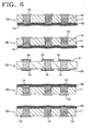
- FIG. 6 shows a second embodiment of the invention.
- the second embodiment differs from the first embodiment in the formation of the diffusing metal layers 16 on the conductor circuits 51 and 52 of the core substrate 50.
- the metal conductor 14 filling each via hole 13 of the one-side printed wiring board 30 desirably projects slightly from the surface of the insulating substrate 11. Since the metal junction having a high strength and good electrical characteristic is obtained in this embodiment as in the foregoing embodiment, high reliability is obtained in the electrical connection.
- the present invention can provide a method of fabricating a printed wiring board and multilayer printed wiring board in which a multilayer printed wiring board having high reliability in the electrical connection between layers.
Abstract
Description
- The present invention relates to a multilayer printed wiring board with an interstitial via hole structure.
- A multilayer printed wiring board having an interstitial via hole structure is conventionally fabricated in the following manner. Via holes are formed in a one-side copper-clad laminate so as to extend through an insulating substrate. Each via hole is filled with an electrically conductive paste or a metal conductor by means of copper plating so that the paste or conductor projects from a surface of the insulating substrate. On the other hand, a copper foil is formed by etching into pads on another printed wiring board to be laminated. Both printed wiring boards are bonded together by thermocompression bonding with an adhesive agent such as epoxy being interposed therebetween. As a result, both printed wiring boards are laminated with the adhesive agent therebetween, and a distal end of each metal conductor of the one printed wiring board is brought into contact with the corresponding pad of the other printed wiring board so that the printed wiring boards are electrically connected together.
- In the foregoing fabricating method, however, the printed wiring boards are electrically connected together by a mechanical contact between each metal conductor slightly projecting from the printed wiring board and the pad. Accordingly, reliability should be still improved. Amethod is provided for electroplating the distal end of each metal conductor with a metal with a low melting point, such as Sn/Pb eutectic solder, for improvement in the reliability. However, since a solder melting at a relatively low temperature is used for connection, the reliability is reduced when the printed wiring board undergoes thermal history such as exposure to high temperature. Moreover, since the solder contains lead, the foregoing method is not preferable from the aspect of an environmental issue.
- A first invention to solve the foregoing problem is a printed wiring board in which a via hole formed in an insulating substrate is filled with a metal conductor, the printed wiring board being laminated with another printed wiring board, and heated and pressed so that a distal end of the metal conductor is abutted against a conductor circuit formed on a surface of said another printed wiring board so that the printed wiring board is electrically connected to said another printed wiring board, characterized in that at least the distal end of the metal conductor or the surface of the conductor circuit has a metal having a melting point higher than a temperature at which both printed wiring boards are pressed and diffusing into the counter metal during press of the printed wiring boards.
- A second invention is characterized in that the conductor circuit formed on the surface of said another printed wiring board or the metal conductor comprise copper and the distal end of the metal conductor is covered with a diffusing metal layer comprising tin.
- A third invention is characterized in that the via hole is filled with the metal conductor by an electroplating.
- A fourth invention is characterized in that the printed wiring boards described in any one of claims 1 to 3 are bonded together by the thermocompression bonding so that the distal end metal of one printed wiring board is diffused into the conductive circuit metal of the other printed wiring board such that both printed wiring boards are electrically connected to each other.
- A fifth invention is a method of fabricating a multilayer printed wiring board, in which a plurality of printed wiring boards are bonded together by thermocompression bonding in a laminated state to be integrated, and a distal end of the metal conductor is pressed against a conductor circuit formed on a surface of said another printed wiring board so that the printed wiring board is electrically connected to said another printed wiring board, characterized by the step of forming a via hole in an insulating substrate of said one printed wiring board, the step of filling the via hole with a metal conductor, the step of forming a diffusing metal layer comprising a metal having a melting point higher than a temperature at which both printed wiring boards are bonded together by the thermocompression bonding and diffusing into the counter metal during the thermocompression bonding of the printed wiring boards, and the step of bonding both printed wiring boards by thermocompression bonding with the metal conductor being pressed against the conductor circuit of the counter printed wiring board.
- A sixth invention is characterized in that a surface roughening process is applied to either one or both of the distal end of the metal conductor and the surface of the conductor circuit before the thermocompression bonding of both printed wiring boards.
- According to the first invention of the printed wiring board and the fifth invention of the method of fabricating the multilayer printed wiring board, the printed wiring board is laminated with another printed wiring board, and both printed wiring boards are bonded together by the thermocompression bonding while the metal conductor of one board is pressed against the conductor circuit of the other board. In this case, pressure acting upon an interface causes diffusion of the metal even if at least the distal end of the metal conductor or the surface of the conductor circuit comprises a metal having a melting point higher than the temperature of thermocompression bonding. As a result, metal junction having a high strength and good electrical characteristic can be obtained. Accordingly, even when the multilayer printed wiring board undergoes thermal history such as exposure to high temperature, the junction is hard to be loosened and high reliability is obtained in the electrical connection. In this case, the metal diffusion takes place earlier when either one or both of the surfaces of the metal conductor and conductor circuit are roughened. Further, when the surface roughening process is previously applied to the contact surface, a contacting surface area is increased such that the metal diffusion is rendered smoother.
- In the second invention, the conductor circuit and the metal conductor are made from copper and accordingly each has a low resistivity. Moreover, tin on the surface of copper of one element diffuses into copper such that a copper-tin alloy layer having a high melting point is formed. Further, according to the printed wiring board of claim 3 in which the via hole is filled with the metal conductor by the electroplating, the density of the metal conductor is increased such that the resistivity is reduced.
- In each invention, the insulating substrate is preferably a glass cloth epoxy resin substrate, glass cloth bismaleimidetriazine resin substrate, glass cloth polyphenylene ether resin substrate or aramid unwoven fabric-polyimide resin substrate. The adhesive agent bonding the printed wiring boards in the laminated state is preferably a thermosetting epoxy adhesive. In this case, the temperature preferably ranges between 180°C and 230°C, and the pressure preferably ranges between 10 and 60 kg/cm2. The thermocompression bonding is preferably carried out under reduced pressure.
-
- FIG. 1 is a sectional view showing steps of fabricating a multilayer printed wiring board of a first embodiment in accordance with the present invention;
- FIG. 2 is a sectional view showing a first half of steps of fabricating a one-side printed wiring board;
- FIG. 3 is a sectional view showing a second half of steps of fabricating the one-side printed wiring board;
- FIG. 4 is a sectional view showing steps of fabricating a core substrate;
- FIG. 5 is a typical sectional view of a junction between a metal conductor and a conductor circuit; and
- FIG. 6 is a sectional view showing steps of fabricating a multilayer printed wiring board of a second embodiment in accordance with the present invention.
-
- FIG. 1(B) illustrates a multilayer printed
wiring board 100 of the embodiment in the completed state . The multilayer printedwiring board 100 is formed by laminating and bonding a plurality of one-side printedwiring boards 30 on both sides of acore substrate 50 as shown in FIG. 1(A). Firstly, fabricating steps for the one-side printedwiring board 30 will be described with reference to FIG. 2. The fabrication starts with a one-side copper-clad laminate 10. Thelaminate 10 has a well known structure, that is, acopper foil 12 is affixed to one side of an insulating substrate of glass cloth epoxy resin, for example. Laser beams are irradiated onto theinsulating substrate 11 at the insulating substrate side so that viaholes 13 extending through theinsulating substrate 11 are formed so as to assume respective predetermined locations (see FIG. 2(B)). - This laser beam machining is executed by a pulse oscillation CO2 gas laser, for example. Regarding the machining conditions, the pulse energy preferably ranges between 2.0 and 10.0 mJ, the pulse width preferably ranges between 1 and 100 µs, the pulse interval is preferably at or above 0.5 ms, and the number of shots preferably ranges between 3 and 50. A diameter of an opening of each
via hole 13 is recommended to range between 50 and 250 µm. - Thereafter, desmearing is carried out in order that resin remaining in the
via holes 13 may be removed. The desmearing includes oxygen plasma discharge, corona discharge process, treatment of potassium permanganate, etc. and is desirable for ensuring reliability in connection. Eachvia hole 13 is filled with ametal conductor 14 or copper by electroplating with thecopper foil 12 serving as one electrode (see FIG. 2(C)). An upper face of themetal conductor 14 in eachvia hole 13 is preferably coplanar with the surface of theinsulating substrate 11. - Subsequently, after a protecting
sheet 15 is affixed onto the copper foil 12 (see FIG. 2(D)), an acid treatment and a rinsing step are executed. A distal end of eachmetal conductor 14 is covered with adiffusing metal layer 16 having a thickness ranging between 10 and 20 µm and comprising tin, by tinning (see FIG. 3(E)). Anepoxy adhesive 40 is applied to an overall surface of theinsulating substrate 11 at the diffusingmetal layer 16 side. The adhesive 40 is preliminarily dried so as to be half hardened. A protectinglayer 17 is affixed to the adhesive 40 (see FIG. 3(F)). Thereafter, the protectingsheet 15 at thecopper foil 12 side is stripped off, and thecopper foil 12 is formed into a predetermined pattern by known mask-etching method such that aconductor circuit 8 is formed. Thus, the one-side printed.wiring board 30 is completed (see FIG. 3(G)). - The core substrate is fabricated as shown in FIG. 4. The fabrication starts with a one-side copper-
clad laminate 60 having a well known structure, that is, acopper foil 62 is affixed to one side of aninsulating substrate 61. Viaholes 63 extending through the insulatingsubstrate 61 are formed so as to assume respective predetermined locations (see FIG. 4(B)). Each viahole 63 is filled with ametal conductor 64 or copper by electroplating (see FIG. 4(C)). Thereafter, a protectingsheet 65 is affixed onto the copper foil 62 (see FIG. 4(D)). After achemical plating layer 66 is formed on the other side of the insulatingsubstrate 61 opposed to thecopper foil 62, electroplating (panel plating) is carried out with thechemical plating layer 66 serving as an electrode so that an electroplating layer 67 is formed in piles. Afirst conductor circuit 51 is formed by the known etching. After the protectingsheet 65 is stripped off, asecond conductor circuit 52 is formed on theopposite copper foil 62 by the etching. The substrate is then immersed in an etchant of organic acid for soft etching so that the surface of the pattern is roughened, whereby thecore substrate 50 is formed (see FIG. 4(E)). - In order that a multilayer printed
wiring board 100 may be fabricated, two one-side printedwiring boards 30 from which the protectingsheets 17 are stripped off are disposed at both sides of thecore substrate 50 as shown in FIG. 1(A). These are set in a heating vacuum press to be pressurized in a laminated state while being heated at a predetermined temperature. Distal ends of themetal conductors 14 of each one-side printedwiring board 30 are pressed against theconductor circuits core substrate 50 andconductor circuits 18 of the inner one-side printedwiring boards 30. Consequently, the distal ends of themetal conductors 14 press theconductor circuits - The heating temperature is only a temperature at which the
epoxy adhesive 40 hardens even if the heating temperature is at or below the melting point of tin (230°C). For example, the heating temperature is recommended to range between 180°C and 230°C. Further, a relative high pressure ranging between 10 kg/cm2 and 60 kg/cm2 is applied, and the pressurized state is desirably maintained for more than 70 minutes, for example. As a result, the distal ends of themetal conductors 14 formed with the respective diffusingmetal layers 16 of tin are pressed against the copper surfaces of theconductor circuits metal layer 16 so that analloy layer 16A of copper-tin is formed. Further, by the step of thermocompression bonding, the adhesive 40 completely hardens and the printedwiring boards - According to the multilayer printed
wiring board 100 of the embodiment, the pressure acting upon the interface between copper and tin causes diffusion of the metal. As a result, metal junction having a high strength and good electrical characteristic is obtained. Accordingly, even when the multilayer printed wiring board undergoes thermal history such as exposure to high temperature, the junction is hard to be loosened and high reliability is obtained in the electrical connection. - Although tin-plating is applied only to the distal ends of the
metal conductors 14 in the foregoing embodiment, thin tin-plated layers having a thickness ranging from 0.5 to 2 µm may be formed on the counter copper foil (conductor circuits - FIG. 6 shows a second embodiment of the invention. The second embodiment differs from the first embodiment in the formation of the diffusing
metal layers 16 on theconductor circuits core substrate 50. In this case, themetal conductor 14 filling each viahole 13 of the one-side printedwiring board 30 desirably projects slightly from the surface of the insulatingsubstrate 11. Since the metal junction having a high strength and good electrical characteristic is obtained in this embodiment as in the foregoing embodiment, high reliability is obtained in the electrical connection. - The present invention should not be limited by the embodiments described above with reference to the drawings. For example, the following embodiments are included in the technical scope of the present invention. Furthermore, the invention may be practiced in various forms without departing from the principle of the invention.
- (1) Although the metal conductor filling each via hole is formed by the electroplating in the foregoing embodiments, an electrically conductive paste may be formed into the metal conductor.
- (2) Although the first and second conductor circuits are formed by the subtraction method in the foregoing embodiments, the circuits may be formed by an additive method in which an electrically conductive path is formed only in a necessary portion.
-
- The present invention can provide a method of fabricating a printed wiring board and multilayer printed wiring board in which a multilayer printed wiring board having high reliability in the electrical connection between layers.
Claims (6)
- A printed wiring board in which a via hole formed in an insulating substrate is filled with a metal conductor, the printed wiring board being laminated with another printed wiring board, and heated and pressed so that a distal end of the metal conductor is abutted against a conductor circuit formed on a surface of said another printed wiring board so that the printed wiring board is electrically connected to said another printed wiring board, characterized in that at least the distal end of the metal conductor or the surface of the conductor circuit has a metal having a melting point higher than a temperature at which both printed wiring boards are pressed and diffusing into the counter metal during press of the printed wiring boards.
- A printed wiring board according to claim 1, characterized in that the conductor circuit formed on the surface of said another printed wiring board or the metal conductor comprise copper and the distal end of the metal conductor is covered with a diffusing metal layer comprising tin.
- A printed wiring board according to claim 1 or 2, characterized in that the via hole is filled with the metal conductor by an electroplating.
- A multilayer printed wiring board characterized in that the printed wiring boards described in any one of claims 1 to 3 are bonded together by the thermocompression bonding so that the distal end metal of one printed wiring board is diffused into the conductive circuit metal of the other printed wiring board such that both printed wiring boards are electrically connected to each other.
- A method of fabricating a multilayer printed wiring board, in which a plurality of printed wiring boards are bonded together by thermocompression bonding in a laminated state to be integrated, and a distal end of the metal conductor is pressed against a conductor circuit formed on a surface of said another printed wiring board so that the printed wiring board is electrically connected to said another printed wiring board, characterized by the step of forming a via hole in an insulating substrate of said one printed wiring board, the step of filling the via hole with a metal conductor, the step of forming a diffusing metal layer comprising a metal having a melting point higher than a temperature at which both printed wiring boards are bonded together by the thermocompression bonding and diffusing into the counter metal during the thermocompression bonding of the printed wiring boards, and the step of bonding both printed wiring boards by thermocompression bonding with the metal conductor being pressed against the conductor circuit of the counter printed wiring board.
- A method of fabricating a multilayer printed wiring board according to claim 5, characterized in that a surface roughening process is applied to either one or both of the distal end of the metal conductor and the surface of the conductor circuit before the thermocompression bonding of both printed wiring boards.
Applications Claiming Priority (3)
| Application Number | Priority Date | Filing Date | Title |
|---|---|---|---|
| JP2000035406A JP2001230551A (en) | 2000-02-14 | 2000-02-14 | Printed wiring board, multil ayered printed wiring board and its manufacturing method |
| JP2000035406 | 2000-02-14 | ||
| PCT/JP2000/008103 WO2001060136A1 (en) | 2000-02-14 | 2000-11-16 | Printed-circuit board, multilayer printed-circuit board and method of manufacture thereof |
Publications (3)
| Publication Number | Publication Date |
|---|---|
| EP1272019A1 true EP1272019A1 (en) | 2003-01-02 |
| EP1272019A4 EP1272019A4 (en) | 2004-12-29 |
| EP1272019B1 EP1272019B1 (en) | 2007-05-30 |
Family
ID=18559610
Family Applications (1)
| Application Number | Title | Priority Date | Filing Date |
|---|---|---|---|
| EP00976306A Expired - Lifetime EP1272019B1 (en) | 2000-02-14 | 2000-11-16 | Printed-circuit board, multilayer printed-circuit board and method of manufacture thereof |
Country Status (5)
| Country | Link |
|---|---|
| US (1) | US6831235B1 (en) |
| EP (1) | EP1272019B1 (en) |
| JP (1) | JP2001230551A (en) |
| DE (1) | DE60035066T2 (en) |
| WO (1) | WO2001060136A1 (en) |
Cited By (3)
| Publication number | Priority date | Publication date | Assignee | Title |
|---|---|---|---|---|
| EP1545176A1 (en) * | 2002-08-19 | 2005-06-22 | Taiyo Yuden Co., Ltd. | Multilayer printed wiring board and production method therefor |
| EP2157842A1 (en) * | 2007-05-17 | 2010-02-24 | Fujikura, Ltd. | Laminated wiring board and method for manufacturing the same |
| FR2954667A1 (en) * | 2009-12-17 | 2011-06-24 | Thales Sa | Multi-layer printed circuit board for e.g. digital circuit with ultra high frequency, has elementary printed circuit board provided with metal holes that permit inter-connection of two external faces of elementary printed circuit board |
Families Citing this family (8)
| Publication number | Priority date | Publication date | Assignee | Title |
|---|---|---|---|---|
| JP4294967B2 (en) * | 2003-02-13 | 2009-07-15 | デンカAgsp株式会社 | Multilayer wiring board and manufacturing method thereof |
| US7197110B2 (en) * | 2004-11-29 | 2007-03-27 | Motorola, Inc. | Method for determining chemical content of complex structures using X-ray microanalysis |
| KR100722605B1 (en) | 2005-09-02 | 2007-05-28 | 삼성전기주식회사 | Manufacturing method of all layer inner via hall printed circuit board that utilizes the fill plating |
| US7394028B2 (en) * | 2006-02-23 | 2008-07-01 | Agere Systems Inc. | Flexible circuit substrate for flip-chip-on-flex applications |
| JP2009026875A (en) * | 2007-07-18 | 2009-02-05 | Nitto Denko Corp | Wiring circuit board |
| CN101400222B (en) * | 2008-10-20 | 2012-08-22 | 深圳市深南电路有限公司 | Printed circuit board assembly and manufacturing method thereof |
| JP6081693B2 (en) * | 2011-09-12 | 2017-02-15 | 新光電気工業株式会社 | Wiring board and method of manufacturing wiring board |
| KR101410895B1 (en) * | 2012-07-04 | 2014-06-23 | 박승남 | Method for manufacturing multi-layer pcb |
Citations (4)
| Publication number | Priority date | Publication date | Assignee | Title |
|---|---|---|---|---|
| US3953924A (en) * | 1975-06-30 | 1976-05-04 | Rockwell International Corporation | Process for making a multilayer interconnect system |
| EP0793405A2 (en) * | 1996-02-28 | 1997-09-03 | CTS Corporation | Multilayer electronic assembly utilizing a sinterable composition and related method of forming |
| WO1998039781A1 (en) * | 1997-03-06 | 1998-09-11 | Ormet Corporation | Vertically interconnected electronic assemblies and compositions useful therefor |
| US5873161A (en) * | 1996-07-23 | 1999-02-23 | Minnesota Mining And Manufacturing Company | Method of making a Z axis interconnect circuit |
Family Cites Families (7)
| Publication number | Priority date | Publication date | Assignee | Title |
|---|---|---|---|---|
| JP3512225B2 (en) * | 1994-02-28 | 2004-03-29 | 株式会社日立製作所 | Method for manufacturing multilayer wiring board |
| US5909058A (en) * | 1996-09-25 | 1999-06-01 | Kabushiki Kaisha Toshiba | Semiconductor package and semiconductor mounting part |
| JPH11186729A (en) * | 1997-10-14 | 1999-07-09 | Ibiden Co Ltd | Multilayered printed wiring board |
| DE69918205T2 (en) * | 1998-03-18 | 2005-06-30 | Mitsubishi Gas Chemical Co., Inc. | A method of making through-holes by laser, copper-clad laminate suitable for making holes, and filler for making holes |
| US6207259B1 (en) * | 1998-11-02 | 2001-03-27 | Kyocera Corporation | Wiring board |
| JP3619395B2 (en) * | 1999-07-30 | 2005-02-09 | 京セラ株式会社 | Semiconductor device built-in wiring board and manufacturing method thereof |
| JP2001144444A (en) | 1999-11-17 | 2001-05-25 | Ibiden Co Ltd | Multilayer printed wiring board and double sided printed wiring board and method of production |
-
2000
- 2000-02-14 JP JP2000035406A patent/JP2001230551A/en active Pending
- 2000-11-16 EP EP00976306A patent/EP1272019B1/en not_active Expired - Lifetime
- 2000-11-16 WO PCT/JP2000/008103 patent/WO2001060136A1/en active IP Right Grant
- 2000-11-16 US US10/009,776 patent/US6831235B1/en not_active Expired - Lifetime
- 2000-11-16 DE DE60035066T patent/DE60035066T2/en not_active Expired - Lifetime
Patent Citations (5)
| Publication number | Priority date | Publication date | Assignee | Title |
|---|---|---|---|---|
| US3953924A (en) * | 1975-06-30 | 1976-05-04 | Rockwell International Corporation | Process for making a multilayer interconnect system |
| US5948533A (en) * | 1990-02-09 | 1999-09-07 | Ormet Corporation | Vertically interconnected electronic assemblies and compositions useful therefor |
| EP0793405A2 (en) * | 1996-02-28 | 1997-09-03 | CTS Corporation | Multilayer electronic assembly utilizing a sinterable composition and related method of forming |
| US5873161A (en) * | 1996-07-23 | 1999-02-23 | Minnesota Mining And Manufacturing Company | Method of making a Z axis interconnect circuit |
| WO1998039781A1 (en) * | 1997-03-06 | 1998-09-11 | Ormet Corporation | Vertically interconnected electronic assemblies and compositions useful therefor |
Non-Patent Citations (1)
| Title |
|---|
| See also references of WO0160136A1 * |
Cited By (6)
| Publication number | Priority date | Publication date | Assignee | Title |
|---|---|---|---|---|
| EP1545176A1 (en) * | 2002-08-19 | 2005-06-22 | Taiyo Yuden Co., Ltd. | Multilayer printed wiring board and production method therefor |
| EP1545176A4 (en) * | 2002-08-19 | 2009-03-04 | Taiyo Yuden Kk | Multilayer printed wiring board and production method therefor |
| EP2157842A1 (en) * | 2007-05-17 | 2010-02-24 | Fujikura, Ltd. | Laminated wiring board and method for manufacturing the same |
| EP2157842A4 (en) * | 2007-05-17 | 2011-11-30 | Fujikura Ltd | Laminated wiring board and method for manufacturing the same |
| US8502086B2 (en) | 2007-05-17 | 2013-08-06 | Fujikura Ltd. | Laminated wiring board and method for manufacturing the same |
| FR2954667A1 (en) * | 2009-12-17 | 2011-06-24 | Thales Sa | Multi-layer printed circuit board for e.g. digital circuit with ultra high frequency, has elementary printed circuit board provided with metal holes that permit inter-connection of two external faces of elementary printed circuit board |
Also Published As
| Publication number | Publication date |
|---|---|
| DE60035066D1 (en) | 2007-07-12 |
| JP2001230551A (en) | 2001-08-24 |
| EP1272019B1 (en) | 2007-05-30 |
| WO2001060136A1 (en) | 2001-08-16 |
| EP1272019A4 (en) | 2004-12-29 |
| US6831235B1 (en) | 2004-12-14 |
| DE60035066T2 (en) | 2007-10-31 |
Similar Documents
| Publication | Publication Date | Title |
|---|---|---|
| EP1009204B1 (en) | Multilayer printed wiring board and method for manufacturing the same | |
| KR101049390B1 (en) | Multilayer printed wiring board and its manufacturing method | |
| US9711440B2 (en) | Wiring board and method for manufacturing the same | |
| US7968803B2 (en) | Wiring substrate, wiring material, copper-clad laminate, and method of manufacturing the wiring substrate | |
| JP4328485B2 (en) | Circuit board and electronic equipment | |
| EP1069811A2 (en) | Multi-layer wiring board and method for manufacturing the same | |
| US6831235B1 (en) | Printed-circuit board, multilayer printed-circuit board and method of manufacture thereof | |
| KR100722739B1 (en) | Core substrate and multiplayer printed circuit board using paste bump and method of manufacturing thereof | |
| JPWO2005004567A1 (en) | Manufacturing method of component-embedded substrate | |
| JPH11204939A (en) | Multilayer circuit board and manufacture thereof | |
| JPH10190232A (en) | Multilayer interconnection board and its manufacture | |
| KR100671541B1 (en) | A manufacturing method of printed circuit embedded board | |
| JP3167840B2 (en) | Printed wiring board and method for manufacturing printed wiring board | |
| JPH11204943A (en) | Electronic circuit board and manufacture thereof | |
| JP2010153438A (en) | Method of manufacturing substrate with built-in component | |
| JPH1070363A (en) | Method for manufacturing printed wiring board | |
| JP3155565B2 (en) | Manufacturing method of printed wiring board | |
| JPH10261854A (en) | Printed wiring board and manufacturing method thereof | |
| JP2004111701A (en) | Printed wiring board and its manufacturing method | |
| JP4410370B2 (en) | Multilayer circuit board | |
| JP2000165045A (en) | Printed wiring board | |
| JP3509315B2 (en) | Circuit board manufacturing method | |
| JP2000133943A (en) | Manufacture of multilayered board | |
| JPH07235756A (en) | Circuit substrate and its manufacture | |
| JP4892924B2 (en) | Multilayer printed wiring board and manufacturing method thereof |
Legal Events
| Date | Code | Title | Description |
|---|---|---|---|
| PUAI | Public reference made under article 153(3) epc to a published international application that has entered the european phase |
Free format text: ORIGINAL CODE: 0009012 |
|
| 17P | Request for examination filed |
Effective date: 20020822 |
|
| AK | Designated contracting states |
Kind code of ref document: A1 Designated state(s): AT BE CH CY DE DK ES FI FR GB GR IE IT LI LU MC NL PT SE TR |
|
| RBV | Designated contracting states (corrected) |
Designated state(s): AT BE CH CY DE FI GB LI NL |
|
| A4 | Supplementary search report drawn up and despatched |
Effective date: 20041112 |
|
| RBV | Designated contracting states (corrected) |
Designated state(s): DE FI GB NL |
|
| GRAP | Despatch of communication of intention to grant a patent |
Free format text: ORIGINAL CODE: EPIDOSNIGR1 |
|
| GRAS | Grant fee paid |
Free format text: ORIGINAL CODE: EPIDOSNIGR3 |
|
| GRAA | (expected) grant |
Free format text: ORIGINAL CODE: 0009210 |
|
| AK | Designated contracting states |
Kind code of ref document: B1 Designated state(s): DE FI GB NL |
|
| PG25 | Lapsed in a contracting state [announced via postgrant information from national office to epo] |
Ref country code: FI Free format text: LAPSE BECAUSE OF FAILURE TO SUBMIT A TRANSLATION OF THE DESCRIPTION OR TO PAY THE FEE WITHIN THE PRESCRIBED TIME-LIMIT Effective date: 20070530 |
|
| REG | Reference to a national code |
Ref country code: GB Ref legal event code: FG4D |
|
| REF | Corresponds to: |
Ref document number: 60035066 Country of ref document: DE Date of ref document: 20070712 Kind code of ref document: P |
|
| NLV1 | Nl: lapsed or annulled due to failure to fulfill the requirements of art. 29p and 29m of the patents act | ||
| PG25 | Lapsed in a contracting state [announced via postgrant information from national office to epo] |
Ref country code: NL Free format text: LAPSE BECAUSE OF FAILURE TO SUBMIT A TRANSLATION OF THE DESCRIPTION OR TO PAY THE FEE WITHIN THE PRESCRIBED TIME-LIMIT Effective date: 20070530 |
|
| PLBE | No opposition filed within time limit |
Free format text: ORIGINAL CODE: 0009261 |
|
| STAA | Information on the status of an ep patent application or granted ep patent |
Free format text: STATUS: NO OPPOSITION FILED WITHIN TIME LIMIT |
|
| 26N | No opposition filed |
Effective date: 20080303 |
|
| GBPC | Gb: european patent ceased through non-payment of renewal fee |
Effective date: 20071116 |
|
| PG25 | Lapsed in a contracting state [announced via postgrant information from national office to epo] |
Ref country code: GB Free format text: LAPSE BECAUSE OF NON-PAYMENT OF DUE FEES Effective date: 20071116 |
|
| PGFP | Annual fee paid to national office [announced via postgrant information from national office to epo] |
Ref country code: DE Payment date: 20121114 Year of fee payment: 13 |
|
| REG | Reference to a national code |
Ref country code: DE Ref legal event code: R119 Ref document number: 60035066 Country of ref document: DE Effective date: 20140603 |
|
| PG25 | Lapsed in a contracting state [announced via postgrant information from national office to epo] |
Ref country code: DE Free format text: LAPSE BECAUSE OF NON-PAYMENT OF DUE FEES Effective date: 20140603 |