EP1255299A2 - Power semiconductor device with pressure contact - Google Patents
Power semiconductor device with pressure contact Download PDFInfo
- Publication number
- EP1255299A2 EP1255299A2 EP02008374A EP02008374A EP1255299A2 EP 1255299 A2 EP1255299 A2 EP 1255299A2 EP 02008374 A EP02008374 A EP 02008374A EP 02008374 A EP02008374 A EP 02008374A EP 1255299 A2 EP1255299 A2 EP 1255299A2
- Authority
- EP
- European Patent Office
- Prior art keywords
- contact
- circuit board
- components
- power semiconductor
- pressure
- Prior art date
- Legal status (The legal status is an assumption and is not a legal conclusion. Google has not performed a legal analysis and makes no representation as to the accuracy of the status listed.)
- Granted
Links
Images

Classifications
-
- H—ELECTRICITY
- H01—ELECTRIC ELEMENTS
- H01L—SEMICONDUCTOR DEVICES NOT COVERED BY CLASS H10
- H01L24/00—Arrangements for connecting or disconnecting semiconductor or solid-state bodies; Methods or apparatus related thereto
- H01L24/80—Methods for connecting semiconductor or other solid state bodies using means for bonding being attached to, or being formed on, the surface to be connected
- H01L24/82—Methods for connecting semiconductor or other solid state bodies using means for bonding being attached to, or being formed on, the surface to be connected by forming build-up interconnects at chip-level, e.g. for high density interconnects [HDI]
-
- H—ELECTRICITY
- H01—ELECTRIC ELEMENTS
- H01L—SEMICONDUCTOR DEVICES NOT COVERED BY CLASS H10
- H01L23/00—Details of semiconductor or other solid state devices
- H01L23/02—Containers; Seals
- H01L23/04—Containers; Seals characterised by the shape of the container or parts, e.g. caps, walls
- H01L23/043—Containers; Seals characterised by the shape of the container or parts, e.g. caps, walls the container being a hollow construction and having a conductive base as a mounting as well as a lead for the semiconductor body
- H01L23/051—Containers; Seals characterised by the shape of the container or parts, e.g. caps, walls the container being a hollow construction and having a conductive base as a mounting as well as a lead for the semiconductor body another lead being formed by a cover plate parallel to the base plate, e.g. sandwich type
-
- H—ELECTRICITY
- H01—ELECTRIC ELEMENTS
- H01L—SEMICONDUCTOR DEVICES NOT COVERED BY CLASS H10
- H01L24/00—Arrangements for connecting or disconnecting semiconductor or solid-state bodies; Methods or apparatus related thereto
- H01L24/01—Means for bonding being attached to, or being formed on, the surface to be connected, e.g. chip-to-package, die-attach, "first-level" interconnects; Manufacturing methods related thereto
- H01L24/18—High density interconnect [HDI] connectors; Manufacturing methods related thereto
- H01L24/23—Structure, shape, material or disposition of the high density interconnect connectors after the connecting process
- H01L24/24—Structure, shape, material or disposition of the high density interconnect connectors after the connecting process of an individual high density interconnect connector
-
- H—ELECTRICITY
- H01—ELECTRIC ELEMENTS
- H01L—SEMICONDUCTOR DEVICES NOT COVERED BY CLASS H10
- H01L24/00—Arrangements for connecting or disconnecting semiconductor or solid-state bodies; Methods or apparatus related thereto
- H01L24/71—Means for bonding not being attached to, or not being formed on, the surface to be connected
- H01L24/72—Detachable connecting means consisting of mechanical auxiliary parts connecting the device, e.g. pressure contacts using springs or clips
-
- H—ELECTRICITY
- H01—ELECTRIC ELEMENTS
- H01L—SEMICONDUCTOR DEVICES NOT COVERED BY CLASS H10
- H01L25/00—Assemblies consisting of a plurality of individual semiconductor or other solid state devices ; Multistep manufacturing processes thereof
- H01L25/03—Assemblies consisting of a plurality of individual semiconductor or other solid state devices ; Multistep manufacturing processes thereof all the devices being of a type provided for in the same subgroup of groups H01L27/00 - H01L33/00, or in a single subclass of H10K, H10N, e.g. assemblies of rectifier diodes
- H01L25/04—Assemblies consisting of a plurality of individual semiconductor or other solid state devices ; Multistep manufacturing processes thereof all the devices being of a type provided for in the same subgroup of groups H01L27/00 - H01L33/00, or in a single subclass of H10K, H10N, e.g. assemblies of rectifier diodes the devices not having separate containers
- H01L25/07—Assemblies consisting of a plurality of individual semiconductor or other solid state devices ; Multistep manufacturing processes thereof all the devices being of a type provided for in the same subgroup of groups H01L27/00 - H01L33/00, or in a single subclass of H10K, H10N, e.g. assemblies of rectifier diodes the devices not having separate containers the devices being of a type provided for in group H01L29/00
- H01L25/072—Assemblies consisting of a plurality of individual semiconductor or other solid state devices ; Multistep manufacturing processes thereof all the devices being of a type provided for in the same subgroup of groups H01L27/00 - H01L33/00, or in a single subclass of H10K, H10N, e.g. assemblies of rectifier diodes the devices not having separate containers the devices being of a type provided for in group H01L29/00 the devices being arranged next to each other
-
- H—ELECTRICITY
- H05—ELECTRIC TECHNIQUES NOT OTHERWISE PROVIDED FOR
- H05K—PRINTED CIRCUITS; CASINGS OR CONSTRUCTIONAL DETAILS OF ELECTRIC APPARATUS; MANUFACTURE OF ASSEMBLAGES OF ELECTRICAL COMPONENTS
- H05K1/00—Printed circuits
- H05K1/02—Details
- H05K1/14—Structural association of two or more printed circuits
- H05K1/142—Arrangements of planar printed circuit boards in the same plane, e.g. auxiliary printed circuit insert mounted in a main printed circuit
-
- H—ELECTRICITY
- H05—ELECTRIC TECHNIQUES NOT OTHERWISE PROVIDED FOR
- H05K—PRINTED CIRCUITS; CASINGS OR CONSTRUCTIONAL DETAILS OF ELECTRIC APPARATUS; MANUFACTURE OF ASSEMBLAGES OF ELECTRICAL COMPONENTS
- H05K1/00—Printed circuits
- H05K1/02—Details
- H05K1/14—Structural association of two or more printed circuits
- H05K1/147—Structural association of two or more printed circuits at least one of the printed circuits being bent or folded, e.g. by using a flexible printed circuit
-
- H—ELECTRICITY
- H01—ELECTRIC ELEMENTS
- H01L—SEMICONDUCTOR DEVICES NOT COVERED BY CLASS H10
- H01L2224/00—Indexing scheme for arrangements for connecting or disconnecting semiconductor or solid-state bodies and methods related thereto as covered by H01L24/00
- H01L2224/01—Means for bonding being attached to, or being formed on, the surface to be connected, e.g. chip-to-package, die-attach, "first-level" interconnects; Manufacturing methods related thereto
- H01L2224/18—High density interconnect [HDI] connectors; Manufacturing methods related thereto
- H01L2224/23—Structure, shape, material or disposition of the high density interconnect connectors after the connecting process
- H01L2224/24—Structure, shape, material or disposition of the high density interconnect connectors after the connecting process of an individual high density interconnect connector
- H01L2224/2401—Structure
- H01L2224/2402—Laminated, e.g. MCM-L type
-
- H—ELECTRICITY
- H01—ELECTRIC ELEMENTS
- H01L—SEMICONDUCTOR DEVICES NOT COVERED BY CLASS H10
- H01L2224/00—Indexing scheme for arrangements for connecting or disconnecting semiconductor or solid-state bodies and methods related thereto as covered by H01L24/00
- H01L2224/01—Means for bonding being attached to, or being formed on, the surface to be connected, e.g. chip-to-package, die-attach, "first-level" interconnects; Manufacturing methods related thereto
- H01L2224/18—High density interconnect [HDI] connectors; Manufacturing methods related thereto
- H01L2224/23—Structure, shape, material or disposition of the high density interconnect connectors after the connecting process
- H01L2224/24—Structure, shape, material or disposition of the high density interconnect connectors after the connecting process of an individual high density interconnect connector
- H01L2224/241—Disposition
- H01L2224/24151—Connecting between a semiconductor or solid-state body and an item not being a semiconductor or solid-state body, e.g. chip-to-substrate, chip-to-passive
- H01L2224/24221—Connecting between a semiconductor or solid-state body and an item not being a semiconductor or solid-state body, e.g. chip-to-substrate, chip-to-passive the body and the item being stacked
- H01L2224/24225—Connecting between a semiconductor or solid-state body and an item not being a semiconductor or solid-state body, e.g. chip-to-substrate, chip-to-passive the body and the item being stacked the item being non-metallic, e.g. insulating substrate with or without metallisation
- H01L2224/24226—Connecting between a semiconductor or solid-state body and an item not being a semiconductor or solid-state body, e.g. chip-to-substrate, chip-to-passive the body and the item being stacked the item being non-metallic, e.g. insulating substrate with or without metallisation the HDI interconnect connecting to the same level of the item at which the semiconductor or solid-state body is mounted, e.g. the item being planar
-
- H—ELECTRICITY
- H01—ELECTRIC ELEMENTS
- H01L—SEMICONDUCTOR DEVICES NOT COVERED BY CLASS H10
- H01L24/00—Arrangements for connecting or disconnecting semiconductor or solid-state bodies; Methods or apparatus related thereto
- H01L24/01—Means for bonding being attached to, or being formed on, the surface to be connected, e.g. chip-to-package, die-attach, "first-level" interconnects; Manufacturing methods related thereto
- H01L24/26—Layer connectors, e.g. plate connectors, solder or adhesive layers; Manufacturing methods related thereto
- H01L24/28—Structure, shape, material or disposition of the layer connectors prior to the connecting process
- H01L24/29—Structure, shape, material or disposition of the layer connectors prior to the connecting process of an individual layer connector
-
- H—ELECTRICITY
- H01—ELECTRIC ELEMENTS
- H01L—SEMICONDUCTOR DEVICES NOT COVERED BY CLASS H10
- H01L2924/00—Indexing scheme for arrangements or methods for connecting or disconnecting semiconductor or solid-state bodies as covered by H01L24/00
- H01L2924/01—Chemical elements
- H01L2924/01004—Beryllium [Be]
-
- H—ELECTRICITY
- H01—ELECTRIC ELEMENTS
- H01L—SEMICONDUCTOR DEVICES NOT COVERED BY CLASS H10
- H01L2924/00—Indexing scheme for arrangements or methods for connecting or disconnecting semiconductor or solid-state bodies as covered by H01L24/00
- H01L2924/01—Chemical elements
- H01L2924/01005—Boron [B]
-
- H—ELECTRICITY
- H01—ELECTRIC ELEMENTS
- H01L—SEMICONDUCTOR DEVICES NOT COVERED BY CLASS H10
- H01L2924/00—Indexing scheme for arrangements or methods for connecting or disconnecting semiconductor or solid-state bodies as covered by H01L24/00
- H01L2924/01—Chemical elements
- H01L2924/01019—Potassium [K]
-
- H—ELECTRICITY
- H01—ELECTRIC ELEMENTS
- H01L—SEMICONDUCTOR DEVICES NOT COVERED BY CLASS H10
- H01L2924/00—Indexing scheme for arrangements or methods for connecting or disconnecting semiconductor or solid-state bodies as covered by H01L24/00
- H01L2924/01—Chemical elements
- H01L2924/01029—Copper [Cu]
-
- H—ELECTRICITY
- H01—ELECTRIC ELEMENTS
- H01L—SEMICONDUCTOR DEVICES NOT COVERED BY CLASS H10
- H01L2924/00—Indexing scheme for arrangements or methods for connecting or disconnecting semiconductor or solid-state bodies as covered by H01L24/00
- H01L2924/01—Chemical elements
- H01L2924/01033—Arsenic [As]
-
- H—ELECTRICITY
- H01—ELECTRIC ELEMENTS
- H01L—SEMICONDUCTOR DEVICES NOT COVERED BY CLASS H10
- H01L2924/00—Indexing scheme for arrangements or methods for connecting or disconnecting semiconductor or solid-state bodies as covered by H01L24/00
- H01L2924/01—Chemical elements
- H01L2924/01068—Erbium [Er]
-
- H—ELECTRICITY
- H01—ELECTRIC ELEMENTS
- H01L—SEMICONDUCTOR DEVICES NOT COVERED BY CLASS H10
- H01L2924/00—Indexing scheme for arrangements or methods for connecting or disconnecting semiconductor or solid-state bodies as covered by H01L24/00
- H01L2924/01—Chemical elements
- H01L2924/01082—Lead [Pb]
-
- H—ELECTRICITY
- H01—ELECTRIC ELEMENTS
- H01L—SEMICONDUCTOR DEVICES NOT COVERED BY CLASS H10
- H01L2924/00—Indexing scheme for arrangements or methods for connecting or disconnecting semiconductor or solid-state bodies as covered by H01L24/00
- H01L2924/013—Alloys
- H01L2924/014—Solder alloys
-
- H—ELECTRICITY
- H01—ELECTRIC ELEMENTS
- H01L—SEMICONDUCTOR DEVICES NOT COVERED BY CLASS H10
- H01L2924/00—Indexing scheme for arrangements or methods for connecting or disconnecting semiconductor or solid-state bodies as covered by H01L24/00
- H01L2924/06—Polymers
- H01L2924/078—Adhesive characteristics other than chemical
-
- H—ELECTRICITY
- H01—ELECTRIC ELEMENTS
- H01L—SEMICONDUCTOR DEVICES NOT COVERED BY CLASS H10
- H01L2924/00—Indexing scheme for arrangements or methods for connecting or disconnecting semiconductor or solid-state bodies as covered by H01L24/00
- H01L2924/10—Details of semiconductor or other solid state devices to be connected
- H01L2924/11—Device type
- H01L2924/13—Discrete devices, e.g. 3 terminal devices
- H01L2924/1301—Thyristor
-
- H—ELECTRICITY
- H01—ELECTRIC ELEMENTS
- H01L—SEMICONDUCTOR DEVICES NOT COVERED BY CLASS H10
- H01L2924/00—Indexing scheme for arrangements or methods for connecting or disconnecting semiconductor or solid-state bodies as covered by H01L24/00
- H01L2924/10—Details of semiconductor or other solid state devices to be connected
- H01L2924/11—Device type
- H01L2924/14—Integrated circuits
-
- H—ELECTRICITY
- H01—ELECTRIC ELEMENTS
- H01L—SEMICONDUCTOR DEVICES NOT COVERED BY CLASS H10
- H01L2924/00—Indexing scheme for arrangements or methods for connecting or disconnecting semiconductor or solid-state bodies as covered by H01L24/00
- H01L2924/15—Details of package parts other than the semiconductor or other solid state devices to be connected
- H01L2924/151—Die mounting substrate
- H01L2924/156—Material
- H01L2924/15786—Material with a principal constituent of the material being a non metallic, non metalloid inorganic material
- H01L2924/15787—Ceramics, e.g. crystalline carbides, nitrides or oxides
-
- H—ELECTRICITY
- H01—ELECTRIC ELEMENTS
- H01L—SEMICONDUCTOR DEVICES NOT COVERED BY CLASS H10
- H01L2924/00—Indexing scheme for arrangements or methods for connecting or disconnecting semiconductor or solid-state bodies as covered by H01L24/00
- H01L2924/19—Details of hybrid assemblies other than the semiconductor or other solid state devices to be connected
- H01L2924/1901—Structure
- H01L2924/1904—Component type
- H01L2924/19043—Component type being a resistor
-
- H—ELECTRICITY
- H05—ELECTRIC TECHNIQUES NOT OTHERWISE PROVIDED FOR
- H05K—PRINTED CIRCUITS; CASINGS OR CONSTRUCTIONAL DETAILS OF ELECTRIC APPARATUS; MANUFACTURE OF ASSEMBLAGES OF ELECTRICAL COMPONENTS
- H05K1/00—Printed circuits
- H05K1/02—Details
- H05K1/03—Use of materials for the substrate
- H05K1/0306—Inorganic insulating substrates, e.g. ceramic, glass
-
- H—ELECTRICITY
- H05—ELECTRIC TECHNIQUES NOT OTHERWISE PROVIDED FOR
- H05K—PRINTED CIRCUITS; CASINGS OR CONSTRUCTIONAL DETAILS OF ELECTRIC APPARATUS; MANUFACTURE OF ASSEMBLAGES OF ELECTRICAL COMPONENTS
- H05K1/00—Printed circuits
- H05K1/02—Details
- H05K1/14—Structural association of two or more printed circuits
- H05K1/141—One or more single auxiliary printed circuits mounted on a main printed circuit, e.g. modules, adapters
-
- H—ELECTRICITY
- H05—ELECTRIC TECHNIQUES NOT OTHERWISE PROVIDED FOR
- H05K—PRINTED CIRCUITS; CASINGS OR CONSTRUCTIONAL DETAILS OF ELECTRIC APPARATUS; MANUFACTURE OF ASSEMBLAGES OF ELECTRICAL COMPONENTS
- H05K2201/00—Indexing scheme relating to printed circuits covered by H05K1/00
- H05K2201/10—Details of components or other objects attached to or integrated in a printed circuit board
- H05K2201/10613—Details of electrical connections of non-printed components, e.g. special leads
- H05K2201/10954—Other details of electrical connections
- H05K2201/10977—Encapsulated connections
-
- H—ELECTRICITY
- H05—ELECTRIC TECHNIQUES NOT OTHERWISE PROVIDED FOR
- H05K—PRINTED CIRCUITS; CASINGS OR CONSTRUCTIONAL DETAILS OF ELECTRIC APPARATUS; MANUFACTURE OF ASSEMBLAGES OF ELECTRICAL COMPONENTS
- H05K3/00—Apparatus or processes for manufacturing printed circuits
- H05K3/0058—Laminating printed circuit boards onto other substrates, e.g. metallic substrates
- H05K3/0061—Laminating printed circuit boards onto other substrates, e.g. metallic substrates onto a metallic substrate, e.g. a heat sink
-
- H—ELECTRICITY
- H05—ELECTRIC TECHNIQUES NOT OTHERWISE PROVIDED FOR
- H05K—PRINTED CIRCUITS; CASINGS OR CONSTRUCTIONAL DETAILS OF ELECTRIC APPARATUS; MANUFACTURE OF ASSEMBLAGES OF ELECTRICAL COMPONENTS
- H05K3/00—Apparatus or processes for manufacturing printed circuits
- H05K3/36—Assembling printed circuits with other printed circuits
- H05K3/361—Assembling flexible printed circuits with other printed circuits
- H05K3/365—Assembling flexible printed circuits with other printed circuits by abutting, i.e. without alloying process
Definitions
- the invention describes a power semiconductor module with active and / or passive Components, in particular a power converter module according to the preamble of Claim 1.
- Such power semiconductor modules are known several times from the literature. When increasing performance, reliability and durability at the same time reduced manufacturing costs are changing methods of Construction technologies for the individual components are a mandatory requirement.
- the pressure build-up in such pressure-contacted power semiconductor modules is determined by means of achieved a mechanically stable pressure plate.
- the generated pressure directly by means of special configurations of the printing plate, as exemplified in DE 196 48 562 C1 shown, or by means of an elastic pressure accumulator according to the DE 199 03 875 A1, are transferred to the substrate.
- the manufacturing method according to DE 41 32 947 A1 has an extremely complex part Layer structure and the further use of classic solder connections. On efficient construction of power semiconductor modules is therefore not guaranteed.
- the present invention has the task of presenting a power semiconductor module in the at least partially on bond and / or solder connections between the individual Semiconductor components or between semiconductor components and various types Contact areas, e.g. those of the substrate can be dispensed with, at least for State of the art equivalent quality in terms of durability and reliability has and is inexpensive to manufacture.
- An additional task is the To simplify isolation of the individual components from each other.
- the inventive design of the circuit-compatible wiring is at least done partly by means of a flexible printed circuit board instead of the bond connections. Bond connections are made in series, while the connection is made using the flexible PCB only requires a single, quick operation. by virtue of the disadvantages of cohesive connections shown above, especially from Solder connections are limited to as few areas of use as possible. It there are two equivalent alternative solutions.
- the semiconductor components are on the contact surfaces of the ceramic substrate cohesively applied. These contact surfaces of the substrate are configured in this way are that they provide circuit-appropriate connections between the individual Realize semiconductor components.
- the integral connection can be exemplified by Soldering or through a more modern and sometimes flexible connection permitted gluing process can be carried out.
- the further circuit-appropriate Wiring of the semiconductor components to each other and also to other contact areas of the substrate is realized by means of the flexible printed circuit board.
- This circuit board is made by the pressure contact of the module is flush with the first main surfaces of the Semiconductor components connected. This pressure contact exists according to the state of the Technology from a pressure-storing element and a pressure in the system introductory pressure plate. The pressure required for contacting is only through the Connection of the power semiconductor module made with the heat sink. Thus the Complete and reliable electrical contacting of the power semiconductor module simultaneously with the thermal contacting of the power semiconductor module on the Heatsink realized.
- the semiconductor components are integrally, advantageously by means of an adhesive process to attach to the flexible circuit board.
- the circuit-compatible connections both on the substrate and in the flexible Printed circuit boards are implemented analogously to the first embodiment.
- the flexible circuit board can also be used at least for partial contacting of the external Power and / or control connections are used.
- fabric-flush and / or cohesive connection variants conceivable.
- a fabric-flush variant can also the pressure contact of the power semiconductor module for the permanent Connection, i.e. a permanent safe contact.
- the inventive design of the isolation of the individual components from each other is made by a flexible insulation material.
- This insulation material can be pasty or have a foam-like structure.
- the insulation material is preferably applied to the first Main surfaces and the spaces between the components applied.
- the inventive step is then followed in the further manufacturing process Power semiconductor modules applied the flexible circuit board.
- Warts of this type on the side facing the first main surface of the components arranged that a circuit-compatible connection is ensured.
- Pressurization displaces the warts in the places where contact is made the insulation material is required.
- Excess insulation material is removed by suitable Cutouts from the area between the substrate equipped with components and the flexible printed circuit board.
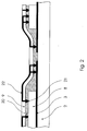
- FIGS. 1 and 2 show a detail of FIG. 1 Housing is omitted for reasons of clarity.
- the cross section is through one having the inventive features Power semiconductor module shown in a structure with a heat sink 1.
- the heat sink 1 is thermally conductively connected to the preferably ceramic substrate 2.
- This Connection by means of a thermal paste, not shown, and also not Flat metal lamination of the second main surface of the substrate 2 has been shown according to the state of the art proven to be extremely suitable for the in Dissipate heat loss resulting from semiconductor modules of the performance class.
- the ceramic substrate 2 which is electrically insulating from the heat sink 1, has its first main surface on contact surfaces 3, which as metallic lamination are trained. These are located on these contact surfaces 3 of the substrate 2 Semiconductor components 8.
- the contact surfaces 3 are designed such that a circuit-compatible connection of the second main surfaces facing the substrate components 8 to be placed thereon.
- the semiconductor components 8 cohesively connected to the contacts 3.
- This integral connection will according to the current state of the art, preferably produced by soldering. there soldering methods are used, which solder all semiconductor components 8 in one Allow operation.
- the circuit-appropriate connection of the respective first, the Main surfaces of the semiconductor components facing away from ceramic are inventively used a flexible circuit board 9 reached.
- This flexible circuit board 9 is not cohesive, but connected flush with the first main surfaces of the semiconductor components. A Permanent and reliable electrical contacting is only possible after the Pressure contact of the entire structure reached.
- the contact surfaces of the flexible circuit board 9 for contacting the In this embodiment, semiconductor components 8 should preferably be wart-like Have elevations 21. On the one hand, these warts ensure a safe one Contacting, on the other hand, can be an efficient pressure contacting of the whole Power semiconductor module are ensured.
- the first Main surfaces of the semiconductor components 8 integrally with the flexible printed circuit board 9 connected is preferably made by means of an electrically conductive Manufactured adhesive.
- a soldering connection is also conceivable.
- the composite of flexible circuit board 9 and semiconductor devices 8 is during the Manufacturing process applied to the substrate 2 such that the second main surfaces the semiconductor components to lie on the contact surfaces 3 of the substrate 2 come that a circuit-compatible contact is established.
- the permanent as well reliable electrical contact with the contact surfaces 3 of the substrate 2 also achieved only after the pressure contact in the overall structure.
- the necessary contacting of power and power semiconductor modules Control connections can also be realized by means of the flexible printed circuit board 9.
- the flexible printed circuit board 9 To are the externally introduced connections on at least one rigid or also flexible circuit board 5 with contacts 6 thereon directly by means of flexible printed circuit board 9 flush with the corresponding connections of the Power semiconductor module by means of those in the power semiconductor module Pressure contact connected.
- the flexible printed circuit board 9 covered for the purpose of contacting the external power and control connections of the Printed circuit board 5 such that at least partially an electrical contact between the corresponding contact areas of the flexible printed circuit board 9 and the contact areas 6 of the external circuit board 5 exists.
- Feedthroughs 12 can also be provided in order to achieve further performance and / or Control connections with the flexible printed circuit board 9, the semiconductor components 8 and / or to allow the contact surfaces 3 of the substrate 2.
- the cavities 4 between the substrate 2 and he flexible printed circuit board 9 can after State of the art for protection against electrical flashovers with a dielectric, for example silicone rubber.
- An inventive embodiment of the isolation of the individual components from one another uses a pasty insulation material 20, which after connecting the Semiconductor components 8 with the contact surfaces 3 of the substrate 2 flat on the latter Composite is applied.
- the flexible placed above this pasty insulation material Printed circuit board 9 is composed of the pressure plate 11 and by means of the pressure contact the pressure accumulator 10 pressed in the direction of the substrate 2.
- the warts are displaced 21 for electrically contacting the flexible printed circuit board 9 with the contact surfaces of the Semiconductor components 28 or the contact surfaces 3 of the substrate 2 in this Insulation material in the area. This creates a long-term stable electrical contact ensured.
Abstract
Description
Die Erfindung beschreibt ein Leistungshalbleitermodul mit aktiven und / oder passiven Bauelementen, insbesondere ein Stromumrichtermodul nach dem Oberbegriff des Anspruches 1. Derartige Leistungshalbleitermodule sind mehrfach aus der Literatur bekannt. Bei der Erhöhung der Leistungsfähigkeit, der Zuverlässigkeit sowie der Lebensdauer bei gleichzeitig verringerten Herstellungskosten sind veränderte Methoden der Aufbautechnologien für die einzelnen Bestandteile eine zwingende Voraussetzung.The invention describes a power semiconductor module with active and / or passive Components, in particular a power converter module according to the preamble of Claim 1. Such power semiconductor modules are known several times from the literature. When increasing performance, reliability and durability at the same time reduced manufacturing costs are changing methods of Construction technologies for the individual components are a mandatory requirement.
Moderne Leistungshalbleitermodule, die Ausgangspunkt dieser Erfindung sind, sind grundplattenlose Module, wie beispielhaft in der DE 199 03 875 A1 beschrieben, bestehend aus
- einem Gehäuse;
- einem keramischen Substrat mit darauf angeordneten schaltungsgerecht ausgeführten metallischen Kaschierungen, wie sie z.B. nach dem DCB- (direct copper bonding) Verfahren hergestellt werden;
- auf diesem Substrat mittels Löttechnik stoffschlüssig aufgebrachten Bauelementen, wie beispielhaft Dioden, Transistoren, Widerständen oder Sensoren;
- Bondverbindungen zur Verbindung der strukturierten Seite der Bauelemente mit weiteren Bauelementen, dem Substrat und / oder nach außen führenden Anschlusselementen.
- Einer vorzugsweise aus Silikonkautschuk bestehenden Vergussmasse zur Isolation der einzelnen Bauelemente zueinander.
- a housing;
- a ceramic substrate with metallic claddings arranged on it in accordance with the circuit, such as those produced by the DCB (direct copper bonding) process;
- components cohesively applied to this substrate by means of soldering technology, such as diodes, transistors, resistors or sensors;
- Bond connections for connecting the structured side of the components to further components, the substrate and / or connecting elements leading to the outside.
- A potting compound preferably made of silicone rubber for isolating the individual components from one another.
Sehr vorteilhaft hat sich für derartige Leistungshalbleitermodule die Aufbautechnologie mit Druckkontakt zur thermischen Kontaktierung des Moduls auf einem Kühlkörper erwiesen. Es hat sich gezeigt, dass sich insbesondere großflächige Lötverbindungen nur sehr schwer qualitätsgerecht beherrschen lassen, worunter die Zuverlässigkeit sowie die Lebensdauer der Leistungshalbleitermodule leiden.The construction technology has also been very advantageous for such power semiconductor modules Pressure contact for thermal contacting of the module on a heat sink has been proven. It has shown that especially large-area soldered connections are very difficult let it be mastered in terms of quality, including reliability and durability of the power semiconductor modules suffer.
Der Druckaufbau in derartigen druckkontaktierten Leistungshalbleitermodulen wird mittels einer mechanisch stabilen Druckplatte erzielt. Je nach weiterer Ausgestaltung kann der erzeugte Druck direkt mittels spezieller Ausgestaltungen der Druckplatte, wie beispielhaft in der DE 196 48 562 C1 gezeigt, oder mittels eines elastischen Druckspeichers nach der DE 199 03 875 A1, auf das Substrat übertragen werden.The pressure build-up in such pressure-contacted power semiconductor modules is determined by means of achieved a mechanically stable pressure plate. Depending on the further configuration, the generated pressure directly by means of special configurations of the printing plate, as exemplified in DE 196 48 562 C1 shown, or by means of an elastic pressure accumulator according to the DE 199 03 875 A1, are transferred to the substrate.
Aus der DE 41 32 947 A1 sind flexible Leiterplatten sowie der Einsatz von elektrisch leitenden und / oder isolierenden Pasten in Leistungshalbleitermodulen bekannt. Diese werden als Ersatz für die keramischen Substrate sowie zur Verbindung zwischen den Bauelementen eingesetzt.DE 41 32 947 A1 describes flexible printed circuit boards and the use of electrical conductive and / or insulating pastes in power semiconductor modules known. This are used as a replacement for the ceramic substrates and for the connection between the Components used.
In der US 4,180,828 wird die Verbindung eines Bauelements mit den Leiterbahnen eines Substrates über eine flexible Folie beschrieben. Der elektrische Kontakt zwischen der Folie und dem Bauelement bzw. zwischen der Folie und den Leiterbahnen wird über Löt- oder Klebeverbindungen hergestellt.In US 4,180,828 the connection of a component with the conductor tracks of a Substrate described on a flexible film. The electrical contact between the film and the component or between the film and the conductor tracks is soldered or Adhesive connections made.
Den Herstellungsverfahren nach DE 196 48 562 C1 oder DE 199 03 875 A1 haftet der Nachteil an, dass, wie bei modernen Modulen üblich, eine Vielzahl von Bauelementen miteinander und / oder mit dem Substrat kontaktiert werden müssen. Bondtechnisch wird dies mittels einer Vielzahl einzelner Bondverbindungen realisiert. Üblich sind hier durchaus bis zu 10 Bondverbindungen pro Bauelement. Da diese Bondverbindungen seriell hergestellt werden, erfordert ihre Herstellung einen erheblichen Zeitaufwand und verursacht damit auch einen wesentlichen Kostenanteil an der Modulherstellung.The manufacturing process according to DE 196 48 562 C1 or DE 199 03 875 A1 is liable The disadvantage is that, as is common with modern modules, a large number of components must be contacted with each other and / or with the substrate. Bond technology becomes this is achieved using a large number of individual bond connections. Are quite common here up to 10 bond connections per component. Because these bond connections are made in series their production takes a considerable amount of time and thus also causes a significant share of costs in module production.
Das Herstellungsverfahren nach DE 41 32 947 A1 weist einen zum Teil äußerst komplexen Schichtaufbau sowie die weitere Verwendung von klassischen Lötverbindungen auf. Ein effizienter Aufbau von Leistungshalbleitermodulen ist somit nicht gewährleistet.The manufacturing method according to DE 41 32 947 A1 has an extremely complex part Layer structure and the further use of classic solder connections. On efficient construction of power semiconductor modules is therefore not guaranteed.
In der US 4,180,828 wird die flexible Folie mittels Löt- oder Klebetechnik auf das Bauelement bzw. auf die Leiterbahnen des Substrates aufgebracht. Die praktische Herstellung derartiger Lötverbindungen gestaltet sich schwierig, da der Wärmeeintrag durch die Folie besondere Techniken erfordert, um eine Beeinträchtigung und / oder Zerstörung der Folie zu vermeiden.In US 4,180,828 the flexible film is applied to the component by means of soldering or adhesive technology or applied to the conductor tracks of the substrate. The practical manufacture of such Solder connections are difficult because the heat input through the foil is special Techniques required to avoid degradation and / or destruction of the film.
Die vorliegende Erfindung hat die Aufgabe ein Leistungshalbleitermodul vorzustellen, bei dem zumindest teilweise auf Bond- und / oder Lötverbindungen zwischen den einzelnen Halbleiterbauelementen bzw. zwischen Halbleiterbauelementen und verschiedenartigen Kontaktflächen, z.B. denen des Substrates, verzichtet werden kann, das mindestens zum Stand der Technik gleichwertige Qualität in Bezug auf Lebensdauer und Zuverlässigkeit aufweist sowie kostengünstig herstellbar ist. Eine zusätzliche Aufgabe besteht darin, die Isolation der einzelnen Bauelemente gegeneinander zu vereinfachen.The present invention has the task of presenting a power semiconductor module in the at least partially on bond and / or solder connections between the individual Semiconductor components or between semiconductor components and various types Contact areas, e.g. those of the substrate can be dispensed with, at least for State of the art equivalent quality in terms of durability and reliability has and is inexpensive to manufacture. An additional task is the To simplify isolation of the individual components from each other.
Die Aufgabe wird gelöst durch die Maßnahmen des kennzeichnenden Teils des Anspruchs 1
sowie die zusätzliche Aufgabe durch die Maßnahmen des kennzeichnenden Teils des
Anspruchs 2 . Weitere vorteilhafte Ausgestaltungen sind in den Unteransprüchen genannt.
Dabei soll im Folgenden unter einer Leiterplatte nicht nur eine im wesentlichen starre
Konstruktion verstanden werden, sondern auch moderne flexible Entwicklungen, wie sie
auch im Stand der Technik beschrieben sind. Diese werden weiterhin als "flexible
Leiterplatten" bezeichnet und sind gekennzeichnet durch einen Aufbau der verschiedene
zueinander sowie zur Oberfläche isolierte Leiterbahnen und zur Oberfläche nicht isolierte
Kontaktflächen zur elektrischen Kontaktierung aufweist,The object is achieved by the measures of the characterizing part of claim 1
as well as the additional task through the measures of the characteristic part of the
Bei der Herstellung kostengünstiger Leistungshalbleitermodule bei gleichzeitig hoher Zuverlässigkeit und Lebensdauer müssen besonders aufwändige Produktionsschritte durch einfachere und schneller zu realisierende Lösungen ersetzt werden. Einen besonderen Zeitaufwand verlangt die Bestückung der Leistungshalbleitermoduls mit den Halbleiterbauelementen und deren anschließende schaltungsgerechte Verdrahtung mittels Bondverbindungen.In the production of inexpensive power semiconductor modules with a high level at the same time Reliability and service life have to go through particularly complex production steps simpler and faster to implement solutions are replaced. A special one It takes time to equip the power semiconductor module with the Semiconductor components and their subsequent circuit-appropriate wiring by means of Bonds.
Die erfinderische Ausgestaltung der schaltungsgerechten Verdrahtung erfolgt zumindest teilweise mittels einer flexiblen Leiterplatte anstelle der Bondverbindungen. Bondverbindungen werden seriell hergestellt, während die Verbindung mittels der flexiblen Leiterplatte nur einen einzigen, schnell durchzuführenden Arbeitsgang erfordert. Aufgrund der oben dargestellten Nachteile stoffschlüssiger Verbindungen speziell von Lötverbindungen wird deren Einsatz auf möglichst wenige Einsatzbereiche beschränkt. Es bieten sich zwei gleichwertige Alternativlösungen an.The inventive design of the circuit-compatible wiring is at least done partly by means of a flexible printed circuit board instead of the bond connections. Bond connections are made in series, while the connection is made using the flexible PCB only requires a single, quick operation. by virtue of the disadvantages of cohesive connections shown above, especially from Solder connections are limited to as few areas of use as possible. It there are two equivalent alternative solutions.
Die Halbleiterbauelemente werden auf die Kontaktflächen des keramischen Substrates stoffschlüssig aufgebracht. Wobei diese Kontaktflächen des Substrates derart ausgestaltet sind, dass sie schaltungsgerechte Verbindungen zwischen den einzeln Halbleiterbauelementen realisieren. Die stoffschlüssige Verbindung kann beispielhaft durch Löten oder durch ein moderneres und zum Teil auch in sich flexible Verbindungen gestattendes Klebeverfahren durchgeführt werden. Die weitere schaltungsgerechte Verdrahtung der Halbleiterbauelemente zueinander und auch zu weiteren Kontaktflächen des Substrates wird mittels der flexiblen Leiterplatte realisiert. Diese Leiterplatte wird durch die Druckkontaktierung des Moduls stoffbündig mit den ersten Hauptflächen der Halbleiterbauelemente verbunden. Diese Druckkontaktierung besteht nach dem Stand der Technik aus einem druckspeichernden Element sowie einer Druck in das System einleitenden Druckplatte. Der zur Kontaktierung notwendige Druck wird erst durch die Verbindung des Leistungshalbleitermoduls mit dem Kühlkörper hergestellt. Somit wird die vollständige und zuverlässige elektrische Kontaktierung des Leistungshalbleitermodul gleichzeitig mit der thermischen Kontaktierung des Leistungshalbleitermodul auf dem Kühlkörper realisiert.The semiconductor components are on the contact surfaces of the ceramic substrate cohesively applied. These contact surfaces of the substrate are configured in this way are that they provide circuit-appropriate connections between the individual Realize semiconductor components. The integral connection can be exemplified by Soldering or through a more modern and sometimes flexible connection permitted gluing process can be carried out. The further circuit-appropriate Wiring of the semiconductor components to each other and also to other contact areas of the substrate is realized by means of the flexible printed circuit board. This circuit board is made by the pressure contact of the module is flush with the first main surfaces of the Semiconductor components connected. This pressure contact exists according to the state of the Technology from a pressure-storing element and a pressure in the system introductory pressure plate. The pressure required for contacting is only through the Connection of the power semiconductor module made with the heat sink. Thus the Complete and reliable electrical contacting of the power semiconductor module simultaneously with the thermal contacting of the power semiconductor module on the Heatsink realized.
Als zweite erfinderische Variante bietet sich an, die Halbleiterbauelemente stoffschlüssig, vorteilhafterweise mittels eines Klebeverfahrens, auf der flexiblen Leiterplatte zu befestigen. Die schaltungsgerechten Verbindungen sowohl auf dem Substrat als auch in der flexiblen Leiterplatte werden analog zur ersten Ausgestaltung realisiert. Durch Aufbringen der mit den Halbleiterbauelementen versehenen flexiblen Leiterplatte auf das Substrat wird die vollständige schaltungsgerechte Verdrahtung des Leistungshalbleitermoduls hergestellt. Die vollständige Funktionsfähigkeit der Verdrahtung wird erst durch die oben beschriebene Druckkontaktierung einschließlich der thermisch leitenden Verbindung mit dem Kühlkörper erzielt.As a second inventive variant, the semiconductor components are integrally, advantageously by means of an adhesive process to attach to the flexible circuit board. The circuit-compatible connections both on the substrate and in the flexible Printed circuit boards are implemented analogously to the first embodiment. By applying the with the Semiconductor components provided flexible circuit board on the substrate complete circuit-compatible wiring of the power semiconductor module. The complete functionality of the wiring is only possible through the one described above Pressure contact including the thermally conductive connection to the heat sink achieved.
Mischformen beider Lösungen können bei speziellen Anwendungsfällen vorteilhaft sein.Mixed forms of both solutions can be advantageous in special applications.
Beide Lösungen besitzen die gleiche vorteilhafte Eigenschaft, dass die Herstellung der stoffbündigen elektrisch leitenden Verbindungen durch die im Leistungshalbleitermodul bereits zur thermischen Kontaktierung auf dem Kühlkörper vorhandene Druckkontaktierung ebenfalls erfolgt.Both solutions have the same advantageous property that the manufacture of the electrically conductive connections through the in the power semiconductor module Pressure contact already present on the heat sink for thermal contacting also done.
Die flexible Leiterplatte kann weiterhin zumindest zur teilweisen Kontaktierung der externen Leistungs- und / oder der Steueranschlüsse dienen. Hier sind ebenfalls stoffbündige und / oder stoffschlüssige Anschlussvarianten denkbar. Bei einer stoffbündigen Variante kann ebenfalls die Druckkontaktierung des Leistungshalbleitermoduls für die dauerhafte Verbindung, d.h. einen dauerhaft sicheren Kontakt, sorgen.The flexible circuit board can also be used at least for partial contacting of the external Power and / or control connections are used. Here are also fabric-flush and / or cohesive connection variants conceivable. For a fabric-flush variant can also the pressure contact of the power semiconductor module for the permanent Connection, i.e. a permanent safe contact.
Die erfinderische Ausgestaltung der Isolation der einzelnen Bauelemente gegeneinander erfolgt durch einen flexiblen Isolationsstoff. Dieser Isolationsstoff kann eine pastöse oder schaumartige Struktur aufweisen. Vorzugsweise wird der Isolationsstoff auf die ersten Hauptflächen sowie die Zwischenräume zwischen den Bauelementen aufgebracht. The inventive design of the isolation of the individual components from each other is made by a flexible insulation material. This insulation material can be pasty or have a foam-like structure. The insulation material is preferably applied to the first Main surfaces and the spaces between the components applied.
Anschließend wird im weiteren Herstellungsprozess der erfinderischen Leistungshalbleitermodule die flexible Leiterplatte aufgebracht. Auf dieser Leiterplatte sind auf der der ersten Hauptfläche der Bauelemente zugewandten Seite Warzen derart angeordnet, dass eine schaltungsgerechte Verbindung sichergestellt ist. Durch die Druckbeaufschlagung verdrängen die Warzen an den Stellen, an denen eine Kontaktierung erforderlich ist, den Isolationsstoff. Überschüssiger Isolationsstoff wird durch geeignete Aussparungen aus dem Bereich zwischen dem mit Bauelementen bestückten Substrat und der flexiblen Leiterplatte herausgepresst. Somit wird mittels der Druckkontaktierung sichergestellt, dass einerseits ein sicherer elektrischer Kontakt zwischen den Bauelementen bzw. den Kontaktflächen des Substrates sowie der flexiblen Leiterplatte hergestellt wird, und andererseits der Zwischenraum zwischen dem mit Bauelementen bestückten Substrat und der flexiblen Leiterplatte vollständig mit isolierendem Material verfüllt ist. Dies sichert die Isolation zwischen den einzelnen Bauelementen.The inventive step is then followed in the further manufacturing process Power semiconductor modules applied the flexible circuit board. Are on this circuit board Warts of this type on the side facing the first main surface of the components arranged that a circuit-compatible connection is ensured. Through the Pressurization displaces the warts in the places where contact is made the insulation material is required. Excess insulation material is removed by suitable Cutouts from the area between the substrate equipped with components and the flexible printed circuit board. Thus, by means of the pressure contact ensures that on the one hand there is a safe electrical contact between the components or the contact surfaces of the substrate and the flexible printed circuit board is produced, and on the other hand, the space between the substrate equipped with components and the flexible printed circuit board is completely filled with insulating material. This secures the Isolation between the individual components.
Spezielle Ausgestaltungen der erfinderischen Lösungen werden an Hand der Fig. 1 und 2 erläutert. Figur 2 zeigt dabei einen Detailausschnitt der Figur 1. Auf die Darstellung eines Gehäuses wird aus Gründen der Übersichtlichkeit verzichtet.Special configurations of the inventive solutions are shown in FIGS. 1 and 2 explained. FIG. 2 shows a detail of FIG. 1 Housing is omitted for reasons of clarity.
In den Figuren ist der Querschnitt durch ein die erfinderischen Merkmale aufweisendes
Leistungshalbleitermodul in einem Aufbau mit einem Kühlkörper 1 gezeigt. Der Kühlkörper 1
ist thermisch leitend mit dem vorzugsweise keramischen Substrat 2 verbunden. Diese
Verbindung mittels einer nicht dargestellten Wärmeleitpaste sowie einer ebenfalls nicht
dargestellten flächigen Metallkaschierung der zweiten Hauptfläche des Substrates 2 hat sich
nach dem Stand der Technik als hervorragend geeignet erwiesen, um die in
Halbleitermodulen der Leistungsklasse entstehende Verlustwärme abzuführen.In the figures, the cross section is through one having the inventive features
Power semiconductor module shown in a structure with a heat sink 1. The heat sink 1
is thermally conductively connected to the preferably
Das gegenüber dem Kühlkörper 1 elektrisch isolierende keramische Substrat 2 weist auf
seiner ersten Hauptfläche Kontaktflächen 3 auf, die als metallische Kaschierungen
ausgebildet sind. Auf diesen Kontaktflächen 3 des Substrates 2 befinden sich die
Halbleiterbauelemente 8. Die Kontaktflächen 3 sind derart gestaltet, dass eine
schaltungsgerechte Verbindung der zweiten, dem Substrat zugewandten, Hauptflächen
darauf zu platzierender Bauelemente 8 erfolgt.The
In einer ersten Ausgestaltung der erfinderischen Lösung sind die Halbleiterbauelemente 8
stoffschlüssig mit den Kontaktierungen 3 verbunden. Diese stoffschlüssige Verbindung wird
nach dem gegenwärtigen Stand der Technik vorzugsweise durch Löten hergestellt. Dabei
werden Lötverfahren angewandt, die eine Lötung aller Halbleiterbauelemente 8 in einem
Arbeitsgang erlauben. Die schaltungsgerechte Verbindung der jeweiligen ersten, der
Keramik abgewandten Hauptflächen der Halbleiterbauelemente wird erfinderisch mittels
einer flexiblen Leiterplatte 9 erreicht. Diese flexible Leiterplatte 9 wird nicht stoffschlüssig,
sondern stoffbündig mit den ersten Hauptflächen der Halbleiterbauelemente verbunden. Eine
dauerhafte sowie zuverlässige elektrische Kontaktierung wird erst nach der
Druckkontaktierung des Gesamtaufbaus erreicht.In a first embodiment of the inventive solution, the
Die Kontaktflächen der flexiblen Leiterplatte 9 zur Kontaktierung mit den
Halbleiterbauelementen 8 sollten bei dieser Ausgestaltung vorzugsweise warzenartige
Erhebungen 21 aufweisen. Diese Warzen gewährleisten einerseits eine sichere
Kontaktierung, andererseits kann damit eine effiziente Druckkontaktierung des gesamten
Leistungshalbleitermoduls sicher gestellt werden.The contact surfaces of the
Bei einer weiteren möglichen Ausgestaltung der erfinderischen Lösung werden die ersten
Hauptflächen der Halbleiterbauelemente 8 stoffschlüssig mit der flexiblen Leiterplatte 9
verbunden. Diese Verbindung wird vorzugsweise mittels eines elektrisch leitfähigen
Klebstoffes hergestellt. Eine löttechnisch Verbindung ist ebenfalls denkbar. Der Verbund aus
flexibler Leiterplatte 9 und Halbleiterbauelementen 8 wird während des
Herstellungsprozesses derart auf das Substrat 2 aufgebracht, dass die zweiten Hauptflächen
der Halbleiterbauelemente derart auf den Kontaktflächen 3 des Substrates 2 zu liegen
kommen, dass eine schaltungsgerechte Kontaktierung hergestellt wird. Die dauerhafte sowie
zuverlässige elektrischen Kontaktierung mit den Kontaktflächen 3 des Substrates 2 wird
ebenfalls erst nach der Druckkontaktierung im Gesamtaufbau erreicht.In a further possible embodiment of the inventive solution, the first
Main surfaces of the
Die bei Leistungshalbleitermodulen notwendige Kontaktierung von Leistungs- und
Steueranschlüssen kann ebenfalls mittels der flexiblen Leiterplatte 9 realisiert werden. Dazu
werden beispielhaft die extern herangeführten Anschlüsse auf mindestens einer starren oder
auch flexiblen Leiterplatte 5 mit darauf befindlichen Kontaktierungen 6 direkt mittels der
flexiblen Leiterplatte 9 stoffbündig mit den entsprechenden Anschlüssen des
Leistungshalbleitermoduls mittels der im Leistungshalbleitermodul vorhandenen
Druckkontaktierung verbunden. Die nicht notwendigerweise die gleiche Dicke wie das
Substrat 2 aufweisenden externen Leiterplatten 5 sind zumindest teilweise mit ihrer zweiten
Hauptfläche elektrisch isoliert auf dem Kühlkörper 1 plaziert. Die flexible Leiterplatte 9
überdeckt zum Zwecke der Kontaktierung der externen Leistungs- und Steueranschlüsse der
Leiterplatte 5 derart, dass zumindest teilweise ein elektrischer Kontakt zwischen den
entsprechenden Kontaktflächen der flexiblen Leiterplatte 9 sowie den Kontaktflächen 6 der
externen Leiterplatte 5 besteht. The necessary contacting of power and power semiconductor modules
Control connections can also be realized by means of the flexible printed
Alle stoffbündigen Kontakte werden erst nach Erstellen der Druckbeaufschlagung mittels
eines elastischen Druckspeichers 10 und einer starren, Druck einleitenden Druckplatte 11,
dauerhaft und zuverlässig geschlossen. Zur Druckeinleitung dient beispielhaft eine
Schraubverbindung. Für diese Schraubverbindungen sind Durchführungen 7, 13, 14, 15 in
der Druckplatte 11, wenn gefordert auch im Druckspeicher 10, dem Substrat 2 und / oder der
externen Leiterplatten 5 vorzusehen. Somit werden bei der Montage auf einem Kühlkörper 1
gleichzeitig sowohl der thermisch leitende, elektrisch isolierende Kontakt des
Leistungshalbleitermoduls zu diesem Kühlkörper 1 als auch alle elektrisch leitenden
stoffbündigen Kontakte hergestellt.All contacts flush with the fabric are only created after the pressure has been applied
an
Weiterhin können Durchführungen 12 vorgesehen werden, um weitere Leistungs- und / oder
Steueranschlüsse mit der flexiblen Leiterplatte 9, den Halbleiterbauelementen 8 und / oder
den Kontaktflächen 3 des Substrates 2 zu erlauben.
Die Hohlräume 4 zwischen dem Substrat 2 sowie er flexiblen Leiterplatte 9 können nach dem
Stand der Technik zur Sicherung gegen elektrische Überschläge mit einem Dielektrikum,
beispielsweise Silikonkautschuk, ausgefüllt sein.The
Eine erfinderische Ausgestaltung der Isolation der einzelnen Bauelemente zueinander
verwendet einen pastösen Isolationsstoff 20, der nach der Verbindung der
Halbleiterbauelemente 8 mit den Kontaktflächen 3 des Substrates 2 flächig auf diesen
Verbund aufgebracht wird. Die oberhalb dieses pastösen Isolationsstoffes platzierte flexible
Leiterplatte 9 wird mittels der Druckkontaktierung bestehend aus der Druckplatte 11 sowie
dem Druckspeicher 10 in Richtung des Substrates 2 gedrückt. Dabei verdrängen die Warzen
21 zur elektrisch Kontaktierung der flexiblen Leiterplatte 9 mit den Kontaktflächen der
Halbleiterbauelemente 28 bzw. den Kontaktflächen 3 des Substrates 2 den in diesem
Bereich befindlichen Isolationsstoff. Somit wird ein langzeitstabiler elektrischer Kontakt
sichergestellt. Weiterhin wird durch die Druckkontaktierung der gesamte verbleibende
Hohlraum zwischen der flexiblen Leiterplatte 9 sowie dem mit Halbleiterbauelementen 8
bestückten Substrat 2 vollständig oder wenn gefordert auch teilweise mit dem Isolationsstoff
ausgefüllt. Überschüssiger Isolationsstoff wird durch geeignete Ausnehmungen oder an den
Rändern des Leistungshalbleitermoduls verdrängt.An inventive embodiment of the isolation of the individual components from one another
uses a
Claims (10)
dadurch gekennzeichnet, dass
die Bauelemente 8 mittels einer zumindest teilweise oberhalb ihrer erster Hauptfläche angeordneten mit Leiterbahnen sowie Kontaktflächen versehenen flexiblen Leiterplatte 9 kontaktiert werden, wobei diese flexible Leiterplatte 9 die Bauelement 8 schaltungsgerecht miteinander und / oder mit den Kontaktflächen 3 des Substrates 2 verbindet und somit die schaltungsgerechte elektrische Verbindung des Moduls bildet und / oder die flexible Leiterplatte 9 die schaltungsgerechte Verbindung zu Kontaktflächen 6 mindestens einer externen Leiterplatte 5 bildet.Power semiconductor module consisting of a housing, a ceramic substrate 2, circuit-oriented structured and electrically conductive contact surfaces 3 arranged thereon, components 8 arranged thereon, a pressure contacting consisting of a flexible pressure accumulator 10 and a pressure-generating pressure plate 11 as well as power and control connections
characterized in that
the components 8 are contacted by means of a flexible printed circuit board 9 arranged at least partially above their first main surface and provided with conductor tracks and contact surfaces, this flexible printed circuit board 9 connecting the components 8 to one another in a circuit-appropriate manner and / or to the contact surfaces 3 of the substrate 2 and thus the circuit-appropriate electrical connection of the module and / or the flexible circuit board 9 forms the circuit-appropriate connection to contact areas 6 of at least one external circuit board 5.
dadurch gekennzeichnet, dass
zur Isolation der Bauelemente 8 gegeneinander ein flexibler Isolationsstoff 20 eingebracht ist, sowie die Kontaktierung der Leiterplatte 9 mit den Bauelementen 8 durch warzenartige Erhebungen 21 derart gebildet wird, dass bei Druckbeaufschlagung mittels der Druckkontaktierung eine sichere elektrisch leitende Verbindung gebildet wird.Power semiconductor module consisting of a housing, a ceramic substrate 2, structured and electrically conductive contact surfaces 3 arranged thereon in accordance with the circuit, components 8 arranged thereon, at least one printed circuit board 9 electrically connecting these components, a pressure contact consisting of a flexible pressure accumulator 10 and a pressure plate 11 generating the pressure as well as power and control connections
characterized in that
a flexible insulation material 20 is introduced to isolate the components 8 from one another, and the contacting of the printed circuit board 9 with the components 8 is formed by wart-like elevations 21 such that a secure electrically conductive connection is formed when pressure is applied by means of the pressure contact.
Applications Claiming Priority (2)
| Application Number | Priority Date | Filing Date | Title |
|---|---|---|---|
| DE10121970A DE10121970B4 (en) | 2001-05-05 | 2001-05-05 | Power semiconductor module in pressure contact |
| DE10121970 | 2001-05-05 |
Publications (3)
| Publication Number | Publication Date |
|---|---|
| EP1255299A2 true EP1255299A2 (en) | 2002-11-06 |
| EP1255299A3 EP1255299A3 (en) | 2006-05-17 |
| EP1255299B1 EP1255299B1 (en) | 2008-01-09 |
Family
ID=7683799
Family Applications (1)
| Application Number | Title | Priority Date | Filing Date |
|---|---|---|---|
| EP02008374A Expired - Lifetime EP1255299B1 (en) | 2001-05-05 | 2002-04-12 | Power semiconductor device with pressure contact |
Country Status (7)
| Country | Link |
|---|---|
| US (1) | US6881071B2 (en) |
| EP (1) | EP1255299B1 (en) |
| JP (1) | JP4194293B2 (en) |
| AT (1) | ATE383658T1 (en) |
| DE (2) | DE10121970B4 (en) |
| DK (1) | DK1255299T3 (en) |
| ES (1) | ES2298303T3 (en) |
Cited By (8)
| Publication number | Priority date | Publication date | Assignee | Title |
|---|---|---|---|---|
| EP1786035A2 (en) * | 2005-11-09 | 2007-05-16 | Semikron Elektronik GmbH & Co. KG Patentabteilung | Circuit arrangement, especially frequency converter |
| EP1855318A1 (en) * | 2006-03-22 | 2007-11-14 | SEMIKRON Elektronik GmbH & Co. KG | Compact high performance semiconductor module with connecting device |
| CN101409276A (en) * | 2007-09-19 | 2009-04-15 | 塞米克朗电子有限及两合公司 | System with a connection device and at least one semi-conductor construction element |
| EP2557595A1 (en) * | 2011-08-12 | 2013-02-13 | SEMIKRON Elektronik GmbH & Co. KG | Power electronics system with a switching device and a control device |
| CN104157635A (en) * | 2013-05-14 | 2014-11-19 | 赛米控电子股份有限公司 | Power semiconductor module and systems with the same |
| WO2018189276A1 (en) * | 2017-04-11 | 2018-10-18 | Audi Ag | Power electronics module |
| EP3439028A1 (en) | 2017-08-03 | 2019-02-06 | Siemens Aktiengesellschaft | Power module with at least one power semiconductor |
| EP4132233A4 (en) * | 2021-03-19 | 2023-12-27 | BOE Technology Group Co., Ltd. | Circuit board module |
Families Citing this family (41)
| Publication number | Priority date | Publication date | Assignee | Title |
|---|---|---|---|---|
| DE10258565B3 (en) * | 2002-12-14 | 2004-08-12 | Semikron Elektronik Gmbh | Circuit arrangement for semiconductor components and method for the production |
| DE10355925B4 (en) | 2003-11-29 | 2006-07-06 | Semikron Elektronik Gmbh & Co. Kg | Power semiconductor module and method of its manufacture |
| DE102004018469B3 (en) * | 2004-04-16 | 2005-10-06 | eupec Europäische Gesellschaft für Leistungshalbleiter mbH | Power semiconductor circuit |
| DE102004018468A1 (en) * | 2004-04-16 | 2006-02-16 | eupec Europäische Gesellschaft für Leistungshalbleiter mbH | Process for the structured application of a laminatable film to a substrate for a semiconductor module |
| DE102004018476B4 (en) | 2004-04-16 | 2009-06-18 | Infineon Technologies Ag | Power semiconductor arrangement with contacting film and pressing device |
| DE102004026596A1 (en) * | 2004-06-01 | 2006-03-02 | eupec Europäische Gesellschaft für Leistungshalbleiter mbH | Active semiconductor arrangement with at least one module plane and having a raised geometry with a conductive layer to make contact with an upper plane |
| DE102004051039B4 (en) | 2004-10-20 | 2008-06-26 | Semikron Elektronik Gmbh & Co. Kg | Power semiconductor module with pressure contact device |
| DE102004057494A1 (en) | 2004-11-29 | 2006-06-08 | Siemens Ag | Metallized foil for surface contact |
| WO2006063539A1 (en) * | 2004-12-17 | 2006-06-22 | Siemens Aktiengesellschaft | Semiconductor switching module |
| DE102005041174A1 (en) | 2005-08-30 | 2007-03-15 | Infineon Technologies Ag | Power semiconductor device with cables within a housing |
| DE102005047567B3 (en) * | 2005-10-05 | 2007-03-29 | Semikron Elektronik Gmbh & Co. Kg | Power semiconductor module comprises a housing, connecting elements and an electrically insulated substrate arranged within the housing and semiconductor components with a connecting element and an insulating molded body |
| DE102005053398B4 (en) * | 2005-11-09 | 2008-12-24 | Semikron Elektronik Gmbh & Co. Kg | The power semiconductor module |
| DE102006006423B4 (en) * | 2006-02-13 | 2009-06-10 | Semikron Elektronik Gmbh & Co. Kg | Power semiconductor module and associated manufacturing method |
| DE102006006424B4 (en) * | 2006-02-13 | 2011-11-17 | Semikron Elektronik Gmbh & Co. Kg | Arrangement with at least one power semiconductor module and a cooling component and associated manufacturing method |
| DE102006020243B3 (en) | 2006-04-27 | 2008-01-17 | Infineon Technologies Austria Ag | Power semiconductor module as H-bridge circuit and method for producing the same |
| US7442046B2 (en) * | 2006-05-15 | 2008-10-28 | Sony Ericsson Mobile Communications Ab | Flexible circuit connectors |
| DE102006025531A1 (en) * | 2006-06-01 | 2008-04-10 | Semikron Elektronik Gmbh & Co. Kg | Converter module |
| JP4365388B2 (en) * | 2006-06-16 | 2009-11-18 | 株式会社日立製作所 | Semiconductor power module and manufacturing method thereof |
| DE102007006706B4 (en) * | 2007-02-10 | 2011-05-26 | Semikron Elektronik Gmbh & Co. Kg | Circuit arrangement with connecting device and manufacturing method thereof |
| DE102007033288A1 (en) * | 2007-07-17 | 2009-01-22 | Siemens Ag | Electronic component and device with high insulation resistance and method for their production |
| US20090079057A1 (en) * | 2007-09-24 | 2009-03-26 | Infineon Technologies Ag | Integrated circuit device |
| DE102007057346B3 (en) * | 2007-11-28 | 2009-06-10 | Fachhochschule Kiel | Laminated power electronics module |
| DE102009005915B4 (en) * | 2009-01-23 | 2013-07-11 | Semikron Elektronik Gmbh & Co. Kg | Power semiconductor module in pressure contact design |
| DE102009015757A1 (en) * | 2009-04-01 | 2010-10-14 | Siemens Aktiengesellschaft | Pressure support for an electronic circuit |
| DE102009017733B4 (en) * | 2009-04-11 | 2011-12-08 | Semikron Elektronik Gmbh & Co. Kg | Power semiconductor module with a connection device and formed as a contact spring internal connection elements |
| DE102009026558B3 (en) * | 2009-05-28 | 2010-12-02 | Infineon Technologies Ag | Power semiconductor module with movably mounted circuit carriers and method for producing such a power semiconductor module |
| DE102009046403B4 (en) | 2009-11-04 | 2015-05-28 | Semikron Elektronik Gmbh & Co. Kg | Power semiconductor module in pressure contact technology |
| DE102010039824B4 (en) * | 2010-08-26 | 2018-03-29 | Semikron Elektronik Gmbh & Co. Kg | Power module with a flexible connection device |
| DE102011078811B3 (en) * | 2011-07-07 | 2012-05-24 | Semikron Elektronik Gmbh & Co. Kg | Power electronic system with a cooling device |
| DE102011078806B4 (en) * | 2011-07-07 | 2014-10-30 | Semikron Elektronik Gmbh & Co. Kg | Manufacturing method for a power electronic system with a cooling device |
| JP5842489B2 (en) * | 2011-09-14 | 2016-01-13 | 三菱電機株式会社 | Semiconductor device |
| DE102013104949B3 (en) * | 2013-05-14 | 2014-04-24 | Semikron Elektronik Gmbh & Co. Kg | Power electronic switching device and arrangement hereby |
| KR101790237B1 (en) | 2016-05-27 | 2017-11-21 | 한경대학교 산학협력단 | Independent gate tunneling field-effect transistor and method for manufacturing thereof |
| EP3273473B1 (en) * | 2016-07-22 | 2020-09-09 | SEMIKRON Elektronik GmbH & Co. KG | Power electronics switching device, arrangement using the same, and method for producing the switch device |
| EP3273470A1 (en) * | 2016-07-22 | 2018-01-24 | SEMIKRON Elektronik GmbH & Co. KG | Power electronics switching device, arrangement using the same, and method for producing the switch device |
| EP3273474A1 (en) | 2016-07-22 | 2018-01-24 | SEMIKRON Elektronik GmbH & Co. KG | Power electronics switching device, arrangement using the same, and method for producing the switch device |
| CN109545773B (en) * | 2018-11-21 | 2020-09-18 | 北京卫星制造厂有限公司 | High-power chip flexible interconnection module and processing method |
| DE102019116686A1 (en) * | 2019-06-19 | 2020-12-24 | Infineon Technologies Ag | POWER CONVERTER SYSTEM, METHOD FOR MANUFACTURING A POWER CONVERTER SYSTEM AND COMBINED SUBSTRATE FOR A POWER CONVERTER SYSTEM |
| US11776890B2 (en) | 2020-01-13 | 2023-10-03 | Samsung Sdi Co., Ltd. | Power semiconductor device |
| DE102020115831B4 (en) | 2020-06-16 | 2024-03-14 | Semikron Elektronik Gmbh & Co. Kg | Power electronic switching device with a printing device |
| DE102021205632A1 (en) | 2021-06-02 | 2022-12-08 | Zf Friedrichshafen Ag | Half bridge for an electric drive of an electric vehicle or a hybrid vehicle, power module for an inverter and inverter |
Citations (3)
| Publication number | Priority date | Publication date | Assignee | Title |
|---|---|---|---|---|
| US5267867A (en) * | 1992-09-11 | 1993-12-07 | Digital Equipment Corporation | Package for multiple removable integrated circuits |
| US5659952A (en) * | 1994-09-20 | 1997-08-26 | Tessera, Inc. | Method of fabricating compliant interface for semiconductor chip |
| US5856913A (en) * | 1996-04-29 | 1999-01-05 | Semikron Elektronik Gmbh | Multilayer semiconductor device having high packing density |
Family Cites Families (9)
| Publication number | Priority date | Publication date | Assignee | Title |
|---|---|---|---|---|
| US3199067A (en) * | 1963-04-04 | 1965-08-03 | Stutzman Guy Robert | Printed circuit multiple connector |
| US3501832A (en) * | 1966-02-26 | 1970-03-24 | Sony Corp | Method of making electrical wiring and wiring connections for electrical components |
| NL7704773A (en) * | 1977-05-02 | 1978-11-06 | Philips Nv | HYBRID CIRCUIT EQUIPPED WITH SEMICONDUCTOR CIRCUIT. |
| US4657322A (en) * | 1985-10-01 | 1987-04-14 | Tektronix, Inc. | Microwave interconnect |
| US4749120A (en) * | 1986-12-18 | 1988-06-07 | Matsushita Electric Industrial Co., Ltd. | Method of connecting a semiconductor device to a wiring board |
| DE4132947C2 (en) * | 1991-10-04 | 1998-11-26 | Export Contor Ausenhandelsgese | Electronic circuitry |
| DE19648562C2 (en) * | 1996-11-23 | 2001-02-15 | Semikron Elektronik Gmbh | Method and device for current monitoring for semiconductor circuits |
| US6326241B1 (en) * | 1997-12-29 | 2001-12-04 | Visteon Global Technologies, Inc. | Solderless flip-chip assembly and method and material for same |
| DE19903875C2 (en) * | 1999-02-01 | 2001-11-29 | Semikron Elektronik Gmbh | Power semiconductor circuit arrangement, in particular current converter, in pressure contact |
-
2001
- 2001-05-05 DE DE10121970A patent/DE10121970B4/en not_active Expired - Lifetime
-
2002
- 2002-04-12 ES ES02008374T patent/ES2298303T3/en not_active Expired - Lifetime
- 2002-04-12 DK DK02008374T patent/DK1255299T3/en active
- 2002-04-12 AT AT02008374T patent/ATE383658T1/en active
- 2002-04-12 EP EP02008374A patent/EP1255299B1/en not_active Expired - Lifetime
- 2002-04-12 DE DE50211496T patent/DE50211496D1/en not_active Expired - Lifetime
- 2002-04-17 JP JP2002114741A patent/JP4194293B2/en not_active Expired - Lifetime
- 2002-05-02 US US10/138,034 patent/US6881071B2/en not_active Expired - Fee Related
Patent Citations (3)
| Publication number | Priority date | Publication date | Assignee | Title |
|---|---|---|---|---|
| US5267867A (en) * | 1992-09-11 | 1993-12-07 | Digital Equipment Corporation | Package for multiple removable integrated circuits |
| US5659952A (en) * | 1994-09-20 | 1997-08-26 | Tessera, Inc. | Method of fabricating compliant interface for semiconductor chip |
| US5856913A (en) * | 1996-04-29 | 1999-01-05 | Semikron Elektronik Gmbh | Multilayer semiconductor device having high packing density |
Cited By (18)
| Publication number | Priority date | Publication date | Assignee | Title |
|---|---|---|---|---|
| EP1786035A2 (en) * | 2005-11-09 | 2007-05-16 | Semikron Elektronik GmbH & Co. KG Patentabteilung | Circuit arrangement, especially frequency converter |
| EP1786035A3 (en) * | 2005-11-09 | 2010-07-07 | Semikron Elektronik GmbH & Co. KG Patentabteilung | Circuit arrangement, especially frequency converter |
| EP1855318A1 (en) * | 2006-03-22 | 2007-11-14 | SEMIKRON Elektronik GmbH & Co. KG | Compact high performance semiconductor module with connecting device |
| US7626256B2 (en) | 2006-03-22 | 2009-12-01 | Semikron Elektronik Gmbh & Co. Kg | Compact power semiconductor module having a connecting device |
| CN101047172B (en) * | 2006-03-22 | 2010-05-26 | 塞米克朗电子有限及两合公司 | Compact type power semi-conductor module with connecting device |
| CN101409276A (en) * | 2007-09-19 | 2009-04-15 | 塞米克朗电子有限及两合公司 | System with a connection device and at least one semi-conductor construction element |
| EP2040295A3 (en) * | 2007-09-19 | 2011-11-02 | SEMIKRON Elektronik GmbH & Co. KG | System with a connection device and at least one semi-conductor construction element |
| EP2557595A1 (en) * | 2011-08-12 | 2013-02-13 | SEMIKRON Elektronik GmbH & Co. KG | Power electronics system with a switching device and a control device |
| CN104157635A (en) * | 2013-05-14 | 2014-11-19 | 赛米控电子股份有限公司 | Power semiconductor module and systems with the same |
| EP2804213A1 (en) * | 2013-05-14 | 2014-11-19 | SEMIKRON Elektronik GmbH & Co. KG | Semiconductor power module and assembly with the same |
| KR20140134629A (en) * | 2013-05-14 | 2014-11-24 | 세미크론 엘렉트로니크 지엠비에치 앤드 코. 케이지 | Power semiconductor module and arrangement comprising the same |
| CN104157635B (en) * | 2013-05-14 | 2018-03-27 | 赛米控电子股份有限公司 | Power semiconductor modular and the system with the power semiconductor modular |
| WO2018189276A1 (en) * | 2017-04-11 | 2018-10-18 | Audi Ag | Power electronics module |
| US11183489B2 (en) | 2017-04-11 | 2021-11-23 | Audi Ag | Power electronics module |
| EP3439028A1 (en) | 2017-08-03 | 2019-02-06 | Siemens Aktiengesellschaft | Power module with at least one power semiconductor |
| WO2019025314A1 (en) | 2017-08-03 | 2019-02-07 | Siemens Aktiengesellschaft | Power module having at least one power semiconductor |
| US11056447B2 (en) | 2017-08-03 | 2021-07-06 | Siemens Aktiengesellschaft | Power module having at least one power semiconductor |
| EP4132233A4 (en) * | 2021-03-19 | 2023-12-27 | BOE Technology Group Co., Ltd. | Circuit board module |
Also Published As
| Publication number | Publication date |
|---|---|
| DK1255299T3 (en) | 2008-05-26 |
| ATE383658T1 (en) | 2008-01-15 |
| EP1255299A3 (en) | 2006-05-17 |
| US20020173192A1 (en) | 2002-11-21 |
| US6881071B2 (en) | 2005-04-19 |
| DE50211496D1 (en) | 2008-02-21 |
| JP4194293B2 (en) | 2008-12-10 |
| JP2002353408A (en) | 2002-12-06 |
| EP1255299B1 (en) | 2008-01-09 |
| ES2298303T3 (en) | 2008-05-16 |
| DE10121970A1 (en) | 2002-11-28 |
| DE10121970B4 (en) | 2004-05-27 |
Similar Documents
| Publication | Publication Date | Title |
|---|---|---|
| EP1255299B1 (en) | Power semiconductor device with pressure contact | |
| EP1351302B1 (en) | Power semiconductor module | |
| DE102008052029A1 (en) | Semiconductor module with switching components and driver electronics | |
| EP1411549A1 (en) | Semiconductor power module with electrically conducting carbon nanotubes | |
| EP0805494A2 (en) | Semiconductor multilayer power module having high package density | |
| EP2284889A1 (en) | High performance semiconductor module with switch holder and load connection element and corresponding production method | |
| EP1192841B1 (en) | Intelligent power module | |
| EP0368143A2 (en) | Electronic control apparatus | |
| EP3273473B1 (en) | Power electronics switching device, arrangement using the same, and method for producing the switch device | |
| WO2018002321A1 (en) | Modular module | |
| DE102011080153A1 (en) | Power semiconductor module for use at outer wall of motor, has component or contact surface exhibiting direct connection with one substrate and arranged between respective substrates and metallization layer that is attached on substrates | |
| DE19924993A1 (en) | Intelligent power module in sandwich construction | |
| DE102017125052A1 (en) | Power semiconductor module with a switching device and power semiconductor device with such a power semiconductor module | |
| DE102008012256A1 (en) | Electronic component mounting board | |
| DE10258565B3 (en) | Circuit arrangement for semiconductor components and method for the production | |
| DE102007039618B4 (en) | Module for integrated control electronics with a simplified structure | |
| EP2033219A1 (en) | Power housing for semiconductor chips and the arrangement thereof for heat dissipation | |
| DE202016101292U1 (en) | Power semiconductor device | |
| DE10121969C1 (en) | Circuit arrangement in pressure contact and method for its production | |
| DE19924994A1 (en) | Sandwich-structured intelligent power module for building into appliances includes a printed circuit board for a logical unit with a recess fitted with a power substrate on a cooling plate connected by a wire bonding technique. | |
| DE102019126923A1 (en) | Power semiconductor module and method for producing a power semiconductor module | |
| DE102011077469A1 (en) | Solar cell module and method for its production | |
| WO2003071601A2 (en) | Circuit module and method for the production thereof | |
| WO2018046165A1 (en) | Power module | |
| WO2017032613A1 (en) | Light-emitting component |
Legal Events
| Date | Code | Title | Description |
|---|---|---|---|
| PUAI | Public reference made under article 153(3) epc to a published international application that has entered the european phase |
Free format text: ORIGINAL CODE: 0009012 |
|
| AK | Designated contracting states |
Kind code of ref document: A2 Designated state(s): AT BE CH CY DE DK ES FI FR GB GR IE IT LI LU MC NL PT SE TR |
|
| AX | Request for extension of the european patent |
Free format text: AL;LT;LV;MK;RO;SI |
|
| RAP1 | Party data changed (applicant data changed or rights of an application transferred) |
Owner name: SEMIKRON ELEKTRONIK GMBH & CO. KG |
|
| PUAL | Search report despatched |
Free format text: ORIGINAL CODE: 0009013 |
|
| AK | Designated contracting states |
Kind code of ref document: A3 Designated state(s): AT BE CH CY DE DK ES FI FR GB GR IE IT LI LU MC NL PT SE TR |
|
| AX | Request for extension of the european patent |
Extension state: AL LT LV MK RO SI |
|
| 17P | Request for examination filed |
Effective date: 20060413 |
|
| 17Q | First examination report despatched |
Effective date: 20060818 |
|
| AKX | Designation fees paid |
Designated state(s): AT BE CH CY DE DK ES FI FR GB GR IE IT LI LU MC NL PT SE TR |
|
| 17Q | First examination report despatched |
Effective date: 20060818 |
|
| GRAP | Despatch of communication of intention to grant a patent |
Free format text: ORIGINAL CODE: EPIDOSNIGR1 |
|
| GRAS | Grant fee paid |
Free format text: ORIGINAL CODE: EPIDOSNIGR3 |
|
| GRAA | (expected) grant |
Free format text: ORIGINAL CODE: 0009210 |
|
| AK | Designated contracting states |
Kind code of ref document: B1 Designated state(s): AT BE CH CY DE DK ES FI FR GB GR IE IT LI LU MC NL PT SE TR |
|
| REG | Reference to a national code |
Ref country code: GB Ref legal event code: FG4D Free format text: NOT ENGLISH |
|
| REG | Reference to a national code |
Ref country code: CH Ref legal event code: EP |
|
| REG | Reference to a national code |
Ref country code: IE Ref legal event code: FG4D Free format text: LANGUAGE OF EP DOCUMENT: GERMAN |
|
| REF | Corresponds to: |
Ref document number: 50211496 Country of ref document: DE Date of ref document: 20080221 Kind code of ref document: P |
|
| REG | Reference to a national code |
Ref country code: CH Ref legal event code: NV Representative=s name: BRAUNPAT BRAUN EDER AG |
|
| REG | Reference to a national code |
Ref country code: SE Ref legal event code: TRGR |
|
| REG | Reference to a national code |
Ref country code: ES Ref legal event code: FG2A Ref document number: 2298303 Country of ref document: ES Kind code of ref document: T3 |
|
| REG | Reference to a national code |
Ref country code: DK Ref legal event code: T3 |
|
| REG | Reference to a national code |
Ref country code: GB Ref legal event code: R108 |
|
| REG | Reference to a national code |
Ref country code: GB Ref legal event code: R108 Effective date: 20080616 |
|
| ET | Fr: translation filed | ||
| PG25 | Lapsed in a contracting state [announced via postgrant information from national office to epo] |
Ref country code: PT Free format text: LAPSE BECAUSE OF FAILURE TO SUBMIT A TRANSLATION OF THE DESCRIPTION OR TO PAY THE FEE WITHIN THE PRESCRIBED TIME-LIMIT Effective date: 20080609 |
|
| REG | Reference to a national code |
Ref country code: IE Ref legal event code: FD4D |
|
| PG25 | Lapsed in a contracting state [announced via postgrant information from national office to epo] |
Ref country code: IE Free format text: LAPSE BECAUSE OF FAILURE TO SUBMIT A TRANSLATION OF THE DESCRIPTION OR TO PAY THE FEE WITHIN THE PRESCRIBED TIME-LIMIT Effective date: 20080109 |
|
| PLBE | No opposition filed within time limit |
Free format text: ORIGINAL CODE: 0009261 |
|
| STAA | Information on the status of an ep patent application or granted ep patent |
Free format text: STATUS: NO OPPOSITION FILED WITHIN TIME LIMIT |
|
| PG25 | Lapsed in a contracting state [announced via postgrant information from national office to epo] |
Ref country code: MC Free format text: LAPSE BECAUSE OF NON-PAYMENT OF DUE FEES Effective date: 20080430 |
|
| 26N | No opposition filed |
Effective date: 20081010 |
|
| PG25 | Lapsed in a contracting state [announced via postgrant information from national office to epo] |
Ref country code: CY Free format text: LAPSE BECAUSE OF FAILURE TO SUBMIT A TRANSLATION OF THE DESCRIPTION OR TO PAY THE FEE WITHIN THE PRESCRIBED TIME-LIMIT Effective date: 20080109 |
|
| PG25 | Lapsed in a contracting state [announced via postgrant information from national office to epo] |
Ref country code: LU Free format text: LAPSE BECAUSE OF NON-PAYMENT OF DUE FEES Effective date: 20080412 |
|
| PG25 | Lapsed in a contracting state [announced via postgrant information from national office to epo] |
Ref country code: TR Free format text: LAPSE BECAUSE OF FAILURE TO SUBMIT A TRANSLATION OF THE DESCRIPTION OR TO PAY THE FEE WITHIN THE PRESCRIBED TIME-LIMIT Effective date: 20080109 |
|
| PG25 | Lapsed in a contracting state [announced via postgrant information from national office to epo] |
Ref country code: GR Free format text: LAPSE BECAUSE OF FAILURE TO SUBMIT A TRANSLATION OF THE DESCRIPTION OR TO PAY THE FEE WITHIN THE PRESCRIBED TIME-LIMIT Effective date: 20080410 |
|
| PGFP | Annual fee paid to national office [announced via postgrant information from national office to epo] |
Ref country code: CH Payment date: 20120427 Year of fee payment: 11 Ref country code: BE Payment date: 20120420 Year of fee payment: 11 Ref country code: NL Payment date: 20120425 Year of fee payment: 11 Ref country code: DK Payment date: 20120411 Year of fee payment: 11 |
|
| PGFP | Annual fee paid to national office [announced via postgrant information from national office to epo] |
Ref country code: GB Payment date: 20120404 Year of fee payment: 11 Ref country code: SE Payment date: 20120425 Year of fee payment: 11 Ref country code: FI Payment date: 20120404 Year of fee payment: 11 |
|
| PGFP | Annual fee paid to national office [announced via postgrant information from national office to epo] |
Ref country code: ES Payment date: 20120426 Year of fee payment: 11 |
|
| PGFP | Annual fee paid to national office [announced via postgrant information from national office to epo] |
Ref country code: AT Payment date: 20120216 Year of fee payment: 11 |
|
| BERE | Be: lapsed |
Owner name: SEMIKRON ELEKTRONIK G.M.B.H. & CO. KG Effective date: 20130430 |
|
| REG | Reference to a national code |
Ref country code: NL Ref legal event code: V1 Effective date: 20131101 |
|
| REG | Reference to a national code |
Ref country code: CH Ref legal event code: PL |
|
| REG | Reference to a national code |
Ref country code: SE Ref legal event code: EUG |
|
| REG | Reference to a national code |
Ref country code: DK Ref legal event code: EBP Effective date: 20130430 |
|
| REG | Reference to a national code |
Ref country code: AT Ref legal event code: MM01 Ref document number: 383658 Country of ref document: AT Kind code of ref document: T Effective date: 20130430 |
|
| GBPC | Gb: european patent ceased through non-payment of renewal fee |
Effective date: 20130412 |
|
| PG25 | Lapsed in a contracting state [announced via postgrant information from national office to epo] |
Ref country code: BE Free format text: LAPSE BECAUSE OF NON-PAYMENT OF DUE FEES Effective date: 20130430 Ref country code: CH Free format text: LAPSE BECAUSE OF NON-PAYMENT OF DUE FEES Effective date: 20130430 Ref country code: LI Free format text: LAPSE BECAUSE OF NON-PAYMENT OF DUE FEES Effective date: 20130430 Ref country code: SE Free format text: LAPSE BECAUSE OF NON-PAYMENT OF DUE FEES Effective date: 20130413 Ref country code: GB Free format text: LAPSE BECAUSE OF NON-PAYMENT OF DUE FEES Effective date: 20130412 |
|
| PG25 | Lapsed in a contracting state [announced via postgrant information from national office to epo] |
Ref country code: NL Free format text: LAPSE BECAUSE OF NON-PAYMENT OF DUE FEES Effective date: 20131101 Ref country code: FI Free format text: LAPSE BECAUSE OF NON-PAYMENT OF DUE FEES Effective date: 20130412 |
|
| PG25 | Lapsed in a contracting state [announced via postgrant information from national office to epo] |
Ref country code: DK Free format text: LAPSE BECAUSE OF NON-PAYMENT OF DUE FEES Effective date: 20130430 |
|
| REG | Reference to a national code |
Ref country code: ES Ref legal event code: FD2A Effective date: 20140611 |
|
| PG25 | Lapsed in a contracting state [announced via postgrant information from national office to epo] |
Ref country code: ES Free format text: LAPSE BECAUSE OF NON-PAYMENT OF DUE FEES Effective date: 20130413 |
|
| REG | Reference to a national code |
Ref country code: FR Ref legal event code: PLFP Year of fee payment: 15 |
|
| PG25 | Lapsed in a contracting state [announced via postgrant information from national office to epo] |
Ref country code: AT Free format text: THE PATENT HAS BEEN ANNULLED BY A DECISION OF A NATIONAL AUTHORITY Effective date: 20130430 |
|
| REG | Reference to a national code |
Ref country code: FR Ref legal event code: PLFP Year of fee payment: 16 |
|
| REG | Reference to a national code |
Ref country code: FR Ref legal event code: PLFP Year of fee payment: 17 |
|
| PGFP | Annual fee paid to national office [announced via postgrant information from national office to epo] |
Ref country code: DE Payment date: 20210430 Year of fee payment: 20 Ref country code: FR Payment date: 20210421 Year of fee payment: 20 Ref country code: IT Payment date: 20210430 Year of fee payment: 20 |
|
| REG | Reference to a national code |
Ref country code: DE Ref legal event code: R071 Ref document number: 50211496 Country of ref document: DE |