EP1249822A2 - Display device - Google Patents
Display device Download PDFInfo
- Publication number
- EP1249822A2 EP1249822A2 EP20020008340 EP02008340A EP1249822A2 EP 1249822 A2 EP1249822 A2 EP 1249822A2 EP 20020008340 EP20020008340 EP 20020008340 EP 02008340 A EP02008340 A EP 02008340A EP 1249822 A2 EP1249822 A2 EP 1249822A2
- Authority
- EP
- European Patent Office
- Prior art keywords
- signal
- analogue
- image signal
- circuit
- digital
- Prior art date
- Legal status (The legal status is an assumption and is not a legal conclusion. Google has not performed a legal analysis and makes no representation as to the accuracy of the status listed.)
- Withdrawn
Links
Images


Classifications
-
- G—PHYSICS
- G02—OPTICS
- G02F—OPTICAL DEVICES OR ARRANGEMENTS FOR THE CONTROL OF LIGHT BY MODIFICATION OF THE OPTICAL PROPERTIES OF THE MEDIA OF THE ELEMENTS INVOLVED THEREIN; NON-LINEAR OPTICS; FREQUENCY-CHANGING OF LIGHT; OPTICAL LOGIC ELEMENTS; OPTICAL ANALOGUE/DIGITAL CONVERTERS
- G02F1/00—Devices or arrangements for the control of the intensity, colour, phase, polarisation or direction of light arriving from an independent light source, e.g. switching, gating or modulating; Non-linear optics
- G02F1/01—Devices or arrangements for the control of the intensity, colour, phase, polarisation or direction of light arriving from an independent light source, e.g. switching, gating or modulating; Non-linear optics for the control of the intensity, phase, polarisation or colour
- G02F1/13—Devices or arrangements for the control of the intensity, colour, phase, polarisation or direction of light arriving from an independent light source, e.g. switching, gating or modulating; Non-linear optics for the control of the intensity, phase, polarisation or colour based on liquid crystals, e.g. single liquid crystal display cells
- G02F1/133—Constructional arrangements; Operation of liquid crystal cells; Circuit arrangements
-
- G—PHYSICS
- G09—EDUCATION; CRYPTOGRAPHY; DISPLAY; ADVERTISING; SEALS
- G09G—ARRANGEMENTS OR CIRCUITS FOR CONTROL OF INDICATING DEVICES USING STATIC MEANS TO PRESENT VARIABLE INFORMATION
- G09G3/00—Control arrangements or circuits, of interest only in connection with visual indicators other than cathode-ray tubes
- G09G3/20—Control arrangements or circuits, of interest only in connection with visual indicators other than cathode-ray tubes for presentation of an assembly of a number of characters, e.g. a page, by composing the assembly by combination of individual elements arranged in a matrix no fixed position being assigned to or needed to be assigned to the individual characters or partial characters
- G09G3/34—Control arrangements or circuits, of interest only in connection with visual indicators other than cathode-ray tubes for presentation of an assembly of a number of characters, e.g. a page, by composing the assembly by combination of individual elements arranged in a matrix no fixed position being assigned to or needed to be assigned to the individual characters or partial characters by control of light from an independent source
- G09G3/36—Control arrangements or circuits, of interest only in connection with visual indicators other than cathode-ray tubes for presentation of an assembly of a number of characters, e.g. a page, by composing the assembly by combination of individual elements arranged in a matrix no fixed position being assigned to or needed to be assigned to the individual characters or partial characters by control of light from an independent source using liquid crystals
- G09G3/3611—Control of matrices with row and column drivers
- G09G3/3685—Details of drivers for data electrodes
- G09G3/3688—Details of drivers for data electrodes suitable for active matrices only
-
- G—PHYSICS
- G09—EDUCATION; CRYPTOGRAPHY; DISPLAY; ADVERTISING; SEALS
- G09G—ARRANGEMENTS OR CIRCUITS FOR CONTROL OF INDICATING DEVICES USING STATIC MEANS TO PRESENT VARIABLE INFORMATION
- G09G2300/00—Aspects of the constitution of display devices
- G09G2300/08—Active matrix structure, i.e. with use of active elements, inclusive of non-linear two terminal elements, in the pixels together with light emitting or modulating elements
- G09G2300/0809—Several active elements per pixel in active matrix panels
- G09G2300/0842—Several active elements per pixel in active matrix panels forming a memory circuit, e.g. a dynamic memory with one capacitor
- G09G2300/0857—Static memory circuit, e.g. flip-flop
-
- G—PHYSICS
- G09—EDUCATION; CRYPTOGRAPHY; DISPLAY; ADVERTISING; SEALS
- G09G—ARRANGEMENTS OR CIRCUITS FOR CONTROL OF INDICATING DEVICES USING STATIC MEANS TO PRESENT VARIABLE INFORMATION
- G09G2330/00—Aspects of power supply; Aspects of display protection and defect management
- G09G2330/02—Details of power systems and of start or stop of display operation
- G09G2330/021—Power management, e.g. power saving
-
- G—PHYSICS
- G09—EDUCATION; CRYPTOGRAPHY; DISPLAY; ADVERTISING; SEALS
- G09G—ARRANGEMENTS OR CIRCUITS FOR CONTROL OF INDICATING DEVICES USING STATIC MEANS TO PRESENT VARIABLE INFORMATION
- G09G2340/00—Aspects of display data processing
- G09G2340/04—Changes in size, position or resolution of an image
- G09G2340/0407—Resolution change, inclusive of the use of different resolutions for different screen areas
- G09G2340/0428—Gradation resolution change
-
- G—PHYSICS
- G09—EDUCATION; CRYPTOGRAPHY; DISPLAY; ADVERTISING; SEALS
- G09G—ARRANGEMENTS OR CIRCUITS FOR CONTROL OF INDICATING DEVICES USING STATIC MEANS TO PRESENT VARIABLE INFORMATION
- G09G3/00—Control arrangements or circuits, of interest only in connection with visual indicators other than cathode-ray tubes
- G09G3/20—Control arrangements or circuits, of interest only in connection with visual indicators other than cathode-ray tubes for presentation of an assembly of a number of characters, e.g. a page, by composing the assembly by combination of individual elements arranged in a matrix no fixed position being assigned to or needed to be assigned to the individual characters or partial characters
- G09G3/2007—Display of intermediate tones
- G09G3/2011—Display of intermediate tones by amplitude modulation
Definitions
- This invention relates to a display device, specifically to a display device which is incorporated into a portable communication and computing device.
- Fig. 6 shows a circuit diagram corresponding to a single pixel element of a conventional liquid crystal display device.
- a gate signal line 51 and a drain signal line 61 are placed on an insulating substrate (not shown) perpendicular to each other.
- a thin-film transistor (TFT) 72 connected to two signal lines 51, 61, is formed near the intersection of the two signal lines 51, 61.
- a source 11s of the TFT 65 is connected to a display electrode 80 of a liquid crystal 21.
- a storage capacitor element 85 holds the voltage of the display electrode 80 during one field period.
- One terminal 86 of the storage capacitor 85 is connected to the source 11s of the TFT 72 and the other terminal 87 is provided with a voltage common among all the pixel elements.
- the TFT 72 When a scanning signal is applied to the gate signal line 51, the TFT 72 turns to an on-state. Accordingly, an analogue image signal from the drain signal line 61 is applied to the display electrode 80, and the storage capacitor 85 holds the voltage. The voltage of the image signal is applied to the liquid crystal 21 through the display electrode 80, and the liquid crystal 21 aligns in response to the applied voltage for providing a liquid crystal display image.
- this configuration is capable of showing both moving images and still images.
- the display is capable of showing both a moving image and a still image within a single display.
- One such example is to show a still image of a battery within an area of a moving image of a cellular phone display to show the remaining amount of the battery power.
- the configuration shown in Fig. 6 requires a continuous rewriting of each pixel element with the same image signal at each scanning in order to provide a still image. This is basically to show a still-like image in a moving image mode, and the scanning signal needs to activate the TFT 72 at each scanning.
- Japanese Laid-Open Patent Publication No. Hei 8-194205 discloses another configuration for a display device suitable for portable applications.
- This display device has a static memory for each of the pixel elements, as shown in Fig. 7.
- a static memory in which two inverters INV1 and INV2 are positively fed back to each other, holds the image signal. This results in reduced power consumption.
- a switching element 24 controls the resistance between a reference line and a display electrode 80 in response to the divalent digital image signal held by the static memory in order to adjust the biasing of the liquid crystal 21.
- the common electrode receives an AC signal Vcom. Ideally, this configuration does not need to refresh the memory when the image stays still for a period of time.
- the conventional liquid crystal display device is suitable for displaying a full color moving picture in response to the analogue image signal.
- the liquid crystal display device with a static memory for retaining the digital image signal is suitable for displaying a low-depth still picture with low-power consumption.
- the object of this invention is directed to a display device, which can alternate between two kinds of display modes, an analogue display mode and a digital display mode.
- the invention provides a display device including a signal processing circuit for processing a digital image signal and a digital-analogue converter for converting the processed digital image signal into an analogue image signal.
- An analogue image signal amplifier is provided for amplifying the analogue image signal outputted from the digital-analogue converter.
- a static memory circuit is provided for retaining an amplified image signal amplified by the analogue signal amplifier.
- a display circuit is also provided for displaying an image based on the image signal retained in the static memory circuit. In this configuration, the signal processing circuit processes the digital image signal so that the processed digital image signal is converted to one of only two values by the digital-analogue converter.
- the invention also provides a display device including a signal processing circuit for processing a digital image signal and a digital-analogue converter for converting the processed digital image signal into an analogue image signal.
- An analogue signal amplifier is provided for amplifying the analogue image signal outputted from the digital-analogue converter.
- the device has a first display circuit receiving the analogue image signal amplified by the analogue signal amplifier. The first display circuit operates in an analogue display mode based on the analogue image signal.
- the device also has a second display circuit having a static memory circuit for retaining the image signal fed through the digital-analogue converter and the analogue signal amplifier. The second display circuit operates in a digital display mode based on the image signal retained in the static memory circuit.
- the first display circuit or the second display circuit is selected corresponding to the analogue display mode or the digital display mode, respectively, and, when the second display circuit is selected, the signal processing circuit processes the digital image signal so that the processed digital image signal is converted to one of only two values by the digital-analogue converter, the two values being a high level and a low level.
- the analogue signal amplifier can amplify the voltage amplitude of the digital image signal, allowing a simpler design of the display circuit.
- This invention is directed to a display device, which can alternate between two kinds of display modes, an analog display mode and a digital display mode, as described in commonly owned copending U.S. Patent Application Serial No. 09/953,233, entitled “DISPLAY DEVICE AND ITS CONTROL METHOD.”
- U.S. Patent Application Serial No. 09/953,233 entitled “DISPLAY DEVICE AND ITS CONTROL METHOD.”
- the disclosure of U.S. Patent Application Serial No. 09/953,233 is in its entirety incorporated herein by reference.
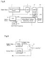
- Fig. 8 shows a display device, which forms a basis of this invention.
- the digital image signal After being processed by the signal processing circuit 1, the digital image signal is converted to the analogue image signal by the DA converter 3, and then inputted to the amplifier 4 in an analogue display mode. Also, the digital image signal, which is written into a static memory, is inputted directly to the amplifier 4, without passing through the DA converter 3, in a digital display mode.
- Fig. 9 shows a configuration of the amplifier of the device of Fig. 8.
- the analogue amplifier 10 amplifies the input analogue image signal.
- the level shifter 11 raises the amplitude of the input digital image signal.
- a switching element 12 is triggered by a display mode switching signal MD. Therefore, under the ordinary display mode (analogue display mode), the analogue image signal amplified by the analogue amplifier 10 is outputted to the liquid crystal display panel 100, and under the digital display mode, the digital image signal amplified by the level shifter 11 is outputted to the liquid crystal display panel 100.
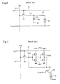
- Fig. 1 shows a circuit diagram of a display device of an embodiment of this invention.
- the signal processing circuit 1 performs the various signal processing tasks such as contrast adjustment and brightness adjustment for the digital image signal inputted from outside.
- the processed digital image signal is converted into the analogue image signal by the DA converter 3, and then inputted to the amplifier 4.
- the analogue amplifier 10 of the amplifier 4 amplifies the analogue image signal.
- the analogue image signal amplified by the analogue amplifier 10 is outputted to the liquid crystal display panel 100.
- the signal processing circuit 1 performs the following signal processing to the digital image signal, the processed signal is outputted to the liquid crystal display device through the DA converter 3 and the amplifier 4. That is, when a corresponding pixel element is to be "white,” the signal processing circuit 1 makes the entire bits of the data "High” ("1") and outputs the high voltage "H” through the DA converter 3. Also, when a corresponding pixel element is to be “black,” the signal processing circuit 1 makes the entire bits of the digital data "Low” ("0") and outputs the low voltage "L” through the DA converter 3.
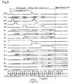
- the signal processing described above is further explained by referring to the output wave shape of the DA converter 3 shown in Fig. 3.
- the output of the DA converter 3 is converted into the analogue image signal corresponding to 16-depth.
- the digital image signal can be written through the analogue amplifier 10.
- the timing control circuit 6 outputs the control signals for controlling the panel drive signal PC, signal processing circuit 1, and the DA converter 3 based on the system clock CLK, horizontal synchronization signal Hsync and the vertical synchronization signal Vsync from the oscillator 5.
- the white/black generating circuit 7 outputs the white signal (signal B) and the black signal (signal A) to the liquid crystal display panel 100 in response to the signal from the timing control circuit 6.
- Reference numeral 8 is the amplifier for amplifying the common electrode drive signal of the liquid crystal.
- a plurality of gate signal lines 51 connected to a gate driver 50 supplying the scanning signal are disposed in one direction.
- a plurality of drain signal lines 61 are disposed in the direction perpendicular to the gate signal line 51.
- the respective sampling transistors SP1, SP2, --- SPn sequentially turn on, supplying a data signal (analogue image signal or digital image signal) of a data signal line 62 to the drain signal line 61.
- a plurality of display pixel elements are disposed in a matrix configuration, which are selected by a scanning signal fed from the gate signal line 51 and which are provided with the data signal fed from the drain signal line 61.
- a circuit selection circuit 40 comprising a P channel TFT 41 and an N channel TFT 42 is formed near the crossing of the gate signal line 51 and drain signal line 61. Both drains of the TFTs 41 and 42 are connected to the drain signal line 61 and both gates of these TFTs are connected to a circuit selection signal line 88. Either one of TFTs 41 or 42 turns on based on a selection signal from the circuit selection signal line 88. Also, as explained later, a circuit selection circuit 43 is formed, making a pair with the circuit selection circuit 40.
- a pixel element selection circuit 70 having an N channel TFT 71 and an N channel TFT 72 is formed adjacent to the circuit selection circuit 40.
- the pixel element selection TFTs 71 and 72 are connected to the circuit selection TFTs 41 and 42 of the circuit selection circuit 40 in vertical direction respectively.
- both gates of the TFTs 71, 72 are connected to the gate signal lines 51. Both of the TFTs 71 and 72 turn on simultaneously in response to the scanning signal fed from the gate signal line 51.
- a storage capacitance element 85 holds the analogue image signal in the analogue mode.
- One electrode 86 of the storage capacitance element 85 is connected to the source 71s of the TFT 71.
- Another electrode 87 is connected to a common storage capacitance line SCL and provided with a bias voltage VCS.
- VCS bias voltage
- a P channel TFT 44 of the circuit selection circuit 43 is placed between the storage capacitance element 85 and the liquid crystal 21, and turns on and off in synchronization with the switching of the TFT 41 of the circuit selection circuit 43.
- a static memory circuit 110 and a signal selection circuit 120 are placed between the TFT 72 of the pixel element selection circuit 70 and the display electrode 80 of the liquid crystal 21.
- the static memory circuit 110 has two inverter circuits, the first and second inverter circuits, which are positively fed back to each other.
- the source 72s of the pixel element selection TFT 72 is connected to an input terminal of the first inverter circuit INV1, and its output is inputted to the second inverter circuit INV2. Also, an output terminal of the second inverter circuit INV2 is connected to the input terminal of the first inverter circuit INV1.
- the signal selection circuit 120 is the circuit selecting the signal based on the digital image signal retained in the static memory circuit 110 and comprises two N-channel TFTs 121, and 122. To the gates of the TFTs 121, 122, the output signal is complimentarily supplied from the static memory circuit 110 and the TFTs 121, 122 complimentarily turn on and off.
- the common electrode signal VCOM (signal B) is selected when the TFT 122 turns on, and the AC drive signal (signal A) is selected when the TFT 121 turns on.
- the selected signal is then applied to the display electrode 80, which supplied the voltage to the liquid crystal 21, through the TFT 45 of the circuit selection circuit 43.
- the liquid crystal panel 100 has peripheral circuit as well.
- An LSI 91 for driver scanning is mounted on an external circuit board 90 retrofitted to the insulating substrate 10 of the liquid crystal panel 100, and sends the vertical start signal STV and the horizontal start signal STH to the gate driver 50 and the drain driver 60, respectively.
- the panel driver LSI also feeds the image signal to the data line 62.
- Fig. 5 shows a timing chart when the liquid crystal display device is set to operate under the digital display mode.
- the analogue image signal is outputted to the data signal line 62 through the DA converter 3 and the amplifier 4. Also, the voltage applied to the circuit selection signal line 88 changes to "L" so that the TFTs 41, 44 of the circuit selection circuits 40, 43 turn on.
- the sampling transistor SP turns on in response to the sampling signal based on the horizontal start signal STH so that the analogue image signal is supplied to the drain signal line 61 through the data signal line 62.
- the scanning signal is supplied to the gate signal line 51 in accordance with the vertical start signal STV.
- the TFT 71 turns on in response to the scanning signal, the analogue image signal Sig is applied through the drain signal line 61 to the display electrode 80 and the storage capacitance element 85, which holds the applied voltage.
- the liquid crystal 21 aligns itself in accordance with the image signal voltage applied to the liquid crystal 21 fed from the display electrode 80, resulting in a display image.
- the analogue display mode is suitable for showing a full color moving picture.
- the data signal line 62 is set to receive the digital image signal.
- the voltage of the circuit selection signal line 88 turns to "H", and the static memory circuit 110 is set to be operable.
- the digital image signal is inputted to the data signal line 62 through the DA converter 3 and the amplifier 4 after being processed by the signal processing circuit 1.
- the TFTs 42 and 45 turn on when the TFTs 41, 44 of the circuit selection circuits 40, 43 turn off.
- the LSI 91 for driver scanning on the external circuit board 90 sends start signals STV, STH to the gate driver 50 and the drain driver 60, respectively.
- the sampling signals are sequentially generated and turn on the respective sampling transistors SP1, SP2, --- SPn sequentially, which sample the digital image signal Sig and send it to each of the drain signal lines 61.
- the scanning signal G1 turns on each TFT of the pixel elements, P11, P12, ---P1n, connected to the gate signal line 51, for one horizontal field period.
- the sampling signal SP1 takes in the digital image signal S11 and feeds it to the drain signal line 61.
- the scanning signal G1 becomes "H", turning the TFT 70 on.
- the drain signal D1 is written into the static memory circuit 110.
- the level of the digital image signal S11 is the divalent output having the high voltage (VH) and the low voltage (VL). Therefore, the writing into the static memory circuit 110 is possible by setting the threshold voltage of the static memory circuit 110 between the high voltage (VH) and the low voltage (VL).
- the signal retained by the static memory circuit 110 is then fed to the signal selection circuit 120, and the signal selection circuit 120 selects one of the signal A and signal B.
- the selected signal is then applied to the liquid crystal 21 through the display electrode 80.
- the display in accordance with the signals held in the static memory circuit 110 appears. Under this digital display mode, the supply of the power voltage to the circuits such as the gate driver 50, the drain driver 60 and the external LSI 91 is halted. In the meantime, the static memory circuit 110 continuously receives the voltages VDD, VSS. Also, the common electrode 32 receives the common electrode voltage and the signal selection circuit 120 receives the signal A and the signal B.
- the liquid crystal display panel 100 when the static memory circuit 110 receives the VDD, VSS for its operation and when the common electrode voltage VCOM is applied to the common electrode, the liquid crystal display panel 100 is in the normally-white (NW) mode. In this mode, the same voltage as the common electrode 32 is applied to the signal B and the AC drive voltage (for example 60HZ) for driving the liquid crystal is applied to the signal A.
- NW normally-white
- the static memory circuit 110 receives the digital image signal of "H (high)" through the drain signal line 61, at the signal selection circuit 120, the first TFT 121 receives an "L” signal and accordingly turns off, and the second TFT 122 receives an "H” signal and accordingly turns on.
- the signal B is selected and the liquid crystal 21 receives the signal B having the same voltage as VCOM applied to the common electrode 32.
- VCOM voltage as VCOM applied to the common electrode 32.
- the static memory circuit 110 receives the digital image signal of "L” through the drain signal line 61, at the signal selection circuit 120, the first TFT 121 receives an "H” signal and accordingly turns on, and the second TFT 122 receives an "L” signal and accordingly turns off.
- the signal A is selected and the liquid crystal 21 receives the signal A, which is the AC drive signal, resulting in the rearrangement of the liquid crystal 21. Since the display panel is in a NW mode, a black image results.
- one-bit digital data signal is used in the digital display mode.
- this invention is not limited to that embodiment, and is also applicable to the multiple-bit digital data signal. In such configuration, a multi gray scale image representation is possible. Also, it is necessary to provide the retaining circuits and the signal selection circuits in accordance with the number of the bits used in the system. Also alternation of the signal processing circuit 1 is required in such application.
- the analogue signal amplifier can be imitatively used as the digital driver. That is, the voltage amplitude of the digital image signal can be amplified by using the analogue signal amplifier, leading to the simplification of the circuit design.
Abstract
Description
- This invention relates to a display device, specifically to a display device which is incorporated into a portable communication and computing device.
- There has been a great demand in the market for portable communication and computing devices such as a portable TV and a cellular phone. All these devices need a small, light-weight and low-power consumption display device, and efforts have been made accordingly.
- Fig. 6 shows a circuit diagram corresponding to a single pixel element of a conventional liquid crystal display device. A
gate signal line 51 and adrain signal line 61 are placed on an insulating substrate (not shown) perpendicular to each other. A thin-film transistor (TFT) 72 connected to twosignal lines signal lines source 11s of the TFT 65 is connected to adisplay electrode 80 of aliquid crystal 21. - A
storage capacitor element 85 holds the voltage of thedisplay electrode 80 during one field period. Oneterminal 86 of thestorage capacitor 85 is connected to thesource 11s of theTFT 72 and theother terminal 87 is provided with a voltage common among all the pixel elements. - When a scanning signal is applied to the
gate signal line 51, theTFT 72 turns to an on-state. Accordingly, an analogue image signal from thedrain signal line 61 is applied to thedisplay electrode 80, and thestorage capacitor 85 holds the voltage. The voltage of the image signal is applied to theliquid crystal 21 through thedisplay electrode 80, and theliquid crystal 21 aligns in response to the applied voltage for providing a liquid crystal display image. - Therefore, this configuration is capable of showing both moving images and still images. There is a need for the display to show both a moving image and a still image within a single display. One such example is to show a still image of a battery within an area of a moving image of a cellular phone display to show the remaining amount of the battery power.
- However, the configuration shown in Fig. 6 requires a continuous rewriting of each pixel element with the same image signal at each scanning in order to provide a still image. This is basically to show a still-like image in a moving image mode, and the scanning signal needs to activate the TFT 72 at each scanning.
- Accordingly, it is necessary to operate a driver circuit which generates a driver signal for the scanning signals and the image signals, and an external LSI which generates various signals for controlling the timing of the driver circuit, resulting in a significant electric power consumption. This is a considerable drawback when such a configuration is used in a cellular phone device which has only a limited power source. That is, the time a user can use the telephone under one battery charge is considerably decreased.
- Japanese Laid-Open Patent Publication No. Hei 8-194205 discloses another configuration for a display device suitable for portable applications. This display device has a static memory for each of the pixel elements, as shown in Fig. 7. A static memory, in which two inverters INV1 and INV2 are positively fed back to each other, holds the image signal. This results in reduced power consumption.
- In this configuration, a
switching element 24 controls the resistance between a reference line and adisplay electrode 80 in response to the divalent digital image signal held by the static memory in order to adjust the biasing of theliquid crystal 21. The common electrode, on the other hand, receives an AC signal Vcom. Ideally, this configuration does not need to refresh the memory when the image stays still for a period of time. - As described above, the conventional liquid crystal display device is suitable for displaying a full color moving picture in response to the analogue image signal. On the other hand, the liquid crystal display device with a static memory for retaining the digital image signal is suitable for displaying a low-depth still picture with low-power consumption.
- However, two liquid crystal display devices described above have different sources for image signals, thus, it is impossible to have both images within single display device.
- Therefore, the object of this invention is directed to a display device, which can alternate between two kinds of display modes, an analogue display mode and a digital display mode.
- The invention lies in the features of the independent claims and preferably in those of the dependent claims.
- The invention provides a display device including a signal processing circuit for processing a digital image signal and a digital-analogue converter for converting the processed digital image signal into an analogue image signal. An analogue image signal amplifier is provided for amplifying the analogue image signal outputted from the digital-analogue converter. A static memory circuit is provided for retaining an amplified image signal amplified by the analogue signal amplifier. A display circuit is also provided for displaying an image based on the image signal retained in the static memory circuit. In this configuration, the signal processing circuit processes the digital image signal so that the processed digital image signal is converted to one of only two values by the digital-analogue converter.
- The invention also provides a display device including a signal processing circuit for processing a digital image signal and a digital-analogue converter for converting the processed digital image signal into an analogue image signal. An analogue signal amplifier is provided for amplifying the analogue image signal outputted from the digital-analogue converter. The device has a first display circuit receiving the analogue image signal amplified by the analogue signal amplifier. The first display circuit operates in an analogue display mode based on the analogue image signal. The device also has a second display circuit having a static memory circuit for retaining the image signal fed through the digital-analogue converter and the analogue signal amplifier. The second display circuit operates in a digital display mode based on the image signal retained in the static memory circuit. In this configuration, the first display circuit or the second display circuit is selected corresponding to the analogue display mode or the digital display mode, respectively, and, when the second display circuit is selected, the signal processing circuit processes the digital image signal so that the processed digital image signal is converted to one of only two values by the digital-analogue converter, the two values being a high level and a low level.
- Accordingly, it is possible to imitatively utilize the analogue signal amplifier as a digital driver. That is, the analogue signal amplifier can amplify the voltage amplitude of the digital image signal, allowing a simpler design of the display circuit.
-
- Fig. 1 is a circuit block diagram of a liquid crystal display device of an embodiment of this invention.
- Fig. 2 is a block diagram of an
amplifier 4 of the embodiment of Fig. 1. - Fig. 3 is a schematic diagram showing a digital-analogue conversion under a digital display mode of the embodiment of Fig. 1.
- Fig. 4 is a circuit diagram of the liquid crystal display device of the embodiment.
- Fig. 5 is a timing chart of the display device under a digital display mode.
- Fig. 6 is a circuit diagram of a conventional liquid crystal display device.
- Fig. 7 is a circuit diagram of another conventional liquid crystal display device.
- Fig. 8 is a circuit block diagram of a liquid crystal display device which provides a basis of this invention.
- Fig. 9 is a block diagram showing a configuration of the amplifier of the liquid crystal display device of Fig. 8.
-
- This invention is directed to a display device, which can alternate between two kinds of display modes, an analog display mode and a digital display mode, as described in commonly owned copending U.S. Patent Application Serial No. 09/953,233, entitled "DISPLAY DEVICE AND ITS CONTROL METHOD." The disclosure of U.S. Patent Application Serial No. 09/953,233 is in its entirety incorporated herein by reference.
- Fig. 8 shows a display device, which forms a basis of this invention. After being processed by the
signal processing circuit 1, the digital image signal is converted to the analogue image signal by theDA converter 3, and then inputted to theamplifier 4 in an analogue display mode. Also, the digital image signal, which is written into a static memory, is inputted directly to theamplifier 4, without passing through theDA converter 3, in a digital display mode. - In Fig. 9 shows a configuration of the amplifier of the device of Fig. 8. The
analogue amplifier 10 amplifies the input analogue image signal. Also, thelevel shifter 11 raises the amplitude of the input digital image signal. - Then, a switching
element 12 is triggered by a display mode switching signal MD. Therefore, under the ordinary display mode (analogue display mode), the analogue image signal amplified by theanalogue amplifier 10 is outputted to the liquidcrystal display panel 100, and under the digital display mode, the digital image signal amplified by thelevel shifter 11 is outputted to the liquidcrystal display panel 100. - Fig. 1 shows a circuit diagram of a display device of an embodiment of this invention.
- The
signal processing circuit 1 performs the various signal processing tasks such as contrast adjustment and brightness adjustment for the digital image signal inputted from outside. The processed digital image signal is converted into the analogue image signal by theDA converter 3, and then inputted to theamplifier 4. - As seen in Fig. 2, the
analogue amplifier 10 of theamplifier 4 amplifies the analogue image signal. Under the ordinary display mode (analogue display mode), the analogue image signal amplified by theanalogue amplifier 10 is outputted to the liquidcrystal display panel 100. - On the other hand, under the digital display mode (under the mode where the image signal is written into a static memory, as mentioned later), after the
signal processing circuit 1 performs the following signal processing to the digital image signal, the processed signal is outputted to the liquid crystal display device through theDA converter 3 and theamplifier 4. That is, when a corresponding pixel element is to be "white," thesignal processing circuit 1 makes the entire bits of the data "High" ("1") and outputs the high voltage "H" through theDA converter 3. Also, when a corresponding pixel element is to be "black," thesignal processing circuit 1 makes the entire bits of the digital data "Low" ("0") and outputs the low voltage "L" through theDA converter 3. - The signal processing described above is further explained by referring to the output wave shape of the
DA converter 3 shown in Fig. 3. When the digital image signal from thesignal processing circuit 1 has a 4-bit configuration, the output of theDA converter 3 is converted into the analogue image signal corresponding to 16-depth. - Under the digital display mode, the entire bits of the digital image signals with "0" at the top bit (0001) --- (0111), is converted into "0s". Also, the entire bits of the digital image signals with "1" at the top bit (1000), (1001), --- (1110) is converted into "1s" Therefore, the digital image signal becomes (1111) when a corresponding pixel element is to be "white," and is converted into (0000) when a corresponding pixel element is to be "black." Thus, when the digital-analogue conversion is performed on the digital image signal processed in the above manner, a divalent output with the high voltage (VH) and the low voltage (VL) is obtained. Also, by amplifying the signal by the
analogue amplifier 10 after the digital-analogue conversion, as shown in Fig. 3, a divalent digital signal with a voltage amplitude of about 3V is obtained. - Therefore, by setting the threshold voltage of the static memory of the liquid crystal display panel between the high voltage (VH) and the low voltage (VL), the digital image signal can be written through the
analogue amplifier 10. - The
timing control circuit 6 outputs the control signals for controlling the panel drive signal PC,signal processing circuit 1, and theDA converter 3 based on the system clock CLK, horizontal synchronization signal Hsync and the vertical synchronization signal Vsync from theoscillator 5. - The white/
black generating circuit 7 outputs the white signal (signal B) and the black signal (signal A) to the liquidcrystal display panel 100 in response to the signal from thetiming control circuit 6.Reference numeral 8 is the amplifier for amplifying the common electrode drive signal of the liquid crystal. - Next, the configuration of the liquid crystal display device, especially the liquid
crystal display panel 100 will be explained by referring to the circuit diagram shown in Fig. 4. - On an insulating substrate, a plurality of
gate signal lines 51 connected to agate driver 50 supplying the scanning signal are disposed in one direction. And a plurality ofdrain signal lines 61 are disposed in the direction perpendicular to thegate signal line 51. - In response to the timing of the sampling pulse outputted from a drain driver 60, the respective sampling transistors SP1, SP2, --- SPn sequentially turn on, supplying a data signal (analogue image signal or digital image signal) of a
data signal line 62 to thedrain signal line 61. - On a liquid
crystal display panel 100, a plurality of display pixel elements are disposed in a matrix configuration, which are selected by a scanning signal fed from thegate signal line 51 and which are provided with the data signal fed from thedrain signal line 61. - The detailed configuration of a
display element 200 will be explained hereinafter. Acircuit selection circuit 40 comprising aP channel TFT 41 and anN channel TFT 42 is formed near the crossing of thegate signal line 51 anddrain signal line 61. Both drains of theTFTs drain signal line 61 and both gates of these TFTs are connected to a circuit selection signal line 88. Either one ofTFTs circuit selection circuit 40. - Therefore the selecting as well as the changing between the analogue display mode (full color moving image) and the digital display mode (low power consumption, still image) becomes possible. Also, a pixel
element selection circuit 70 having anN channel TFT 71 and anN channel TFT 72 is formed adjacent to thecircuit selection circuit 40. The pixelelement selection TFTs circuit selection TFTs circuit selection circuit 40 in vertical direction respectively. Also, both gates of theTFTs TFTs gate signal line 51. - A
storage capacitance element 85 holds the analogue image signal in the analogue mode. Oneelectrode 86 of thestorage capacitance element 85 is connected to thesource 71s of theTFT 71. Anotherelectrode 87 is connected to a common storage capacitance line SCL and provided with a bias voltage VCS. When the analogue image signal is applied to theliquid crystal 21 after the opening of the TFT gates of thecircuit selection circuit 70, the voltage of the applied signal reduces even during a one-field period, resulting in loosing the homogeneity of the display image. Thestorage capacitance element 85 maintains the applied voltage at the initial level during one field period for eliminating the problem above. -
A P channel TFT 44 of the circuit selection circuit 43 is placed between thestorage capacitance element 85 and theliquid crystal 21, and turns on and off in synchronization with the switching of theTFT 41 of the circuit selection circuit 43. Astatic memory circuit 110 and a signal selection circuit 120 are placed between theTFT 72 of the pixelelement selection circuit 70 and thedisplay electrode 80 of theliquid crystal 21. - The
static memory circuit 110 has two inverter circuits, the first and second inverter circuits, which are positively fed back to each other. The source 72s of the pixelelement selection TFT 72 is connected to an input terminal of the first inverter circuit INV1, and its output is inputted to the second inverter circuit INV2. Also, an output terminal of the second inverter circuit INV2 is connected to the input terminal of the first inverter circuit INV1. - Under the digital display mode, when the voltage of the circuit selection signal line 88 as well as the scanning signal of the
gate signal line 51 becomes "H", thestatic memory circuit 110 is ready to for the writing. - The signal selection circuit 120 is the circuit selecting the signal based on the digital image signal retained in the
static memory circuit 110 and comprises two N-channel TFTs TFTs static memory circuit 110 and theTFTs - Here, the common electrode signal VCOM (signal B) is selected when the
TFT 122 turns on, and the AC drive signal (signal A) is selected when theTFT 121 turns on. The selected signal is then applied to thedisplay electrode 80, which supplied the voltage to theliquid crystal 21, through the TFT 45 of the circuit selection circuit 43. - The
liquid crystal panel 100 has peripheral circuit as well. AnLSI 91 for driver scanning is mounted on anexternal circuit board 90 retrofitted to the insulatingsubstrate 10 of theliquid crystal panel 100, and sends the vertical start signal STV and the horizontal start signal STH to thegate driver 50 and the drain driver 60, respectively. The panel driver LSI also feeds the image signal to thedata line 62. - The driving method of the display device described above will be explained hereinafter in reference to Figs. 4 and 5. Fig. 5 shows a timing chart when the liquid crystal display device is set to operate under the digital display mode.
- When the analogue display mode is selected in response to the mode selection signal MD, the analogue image signal is outputted to the data signal
line 62 through theDA converter 3 and theamplifier 4. Also, the voltage applied to the circuit selection signal line 88 changes to "L" so that theTFTs circuit selection circuits 40, 43 turn on. - The sampling transistor SP turns on in response to the sampling signal based on the horizontal start signal STH so that the analogue image signal is supplied to the
drain signal line 61 through the data signalline 62. - Also, the scanning signal is supplied to the
gate signal line 51 in accordance with the vertical start signal STV. When theTFT 71 turns on in response to the scanning signal, the analogue image signal Sig is applied through thedrain signal line 61 to thedisplay electrode 80 and thestorage capacitance element 85, which holds the applied voltage. Theliquid crystal 21 aligns itself in accordance with the image signal voltage applied to theliquid crystal 21 fed from thedisplay electrode 80, resulting in a display image. - The analogue display mode is suitable for showing a full color moving picture.
- When the digital display mode is selected in response to the mode selection signal MD, the data signal
line 62 is set to receive the digital image signal. At the same time, the voltage of the circuit selection signal line 88 turns to "H", and thestatic memory circuit 110 is set to be operable. - Here, as described before, the digital image signal is inputted to the data signal
line 62 through theDA converter 3 and theamplifier 4 after being processed by thesignal processing circuit 1. - Also, the
TFTs 42 and 45 turn on when theTFTs circuit selection circuits 40, 43 turn off. TheLSI 91 for driver scanning on theexternal circuit board 90 sends start signals STV, STH to thegate driver 50 and the drain driver 60, respectively. In response to the start signals, the sampling signals are sequentially generated and turn on the respective sampling transistors SP1, SP2, --- SPn sequentially, which sample the digital image signal Sig and send it to each of the drain signal lines 61. - The operation of the first row of the matrix, or the operation of the
gate signal line 51, which receives the scanning signal G1 will be described below. First, the scanning signal G1 turns on each TFT of the pixel elements, P11, P12, ---P1n, connected to thegate signal line 51, for one horizontal field period. - In the pixel element P11 located at the upper left corner of the matrix, the sampling signal SP1 takes in the digital image signal S11 and feeds it to the
drain signal line 61. The scanning signal G1 becomes "H", turning theTFT 70 on. Thus, the drain signal D1 is written into thestatic memory circuit 110. - Under the digital display mode, the level of the digital image signal S11 is the divalent output having the high voltage (VH) and the low voltage (VL). Therefore, the writing into the
static memory circuit 110 is possible by setting the threshold voltage of thestatic memory circuit 110 between the high voltage (VH) and the low voltage (VL). - The signal retained by the
static memory circuit 110 is then fed to the signal selection circuit 120, and the signal selection circuit 120 selects one of the signal A and signal B. The selected signal is then applied to theliquid crystal 21 through thedisplay electrode 80. Thus, when the scanning is done from the firstgate signal line 51 on the top row of the matrix to the lastgate signal line 51 on the bottom row of the matrix, a full display frame scan (one field scan) is completed. - Then, the display in accordance with the signals held in the static memory circuit 110 (still picture display) appears. Under this digital display mode, the supply of the power voltage to the circuits such as the
gate driver 50, the drain driver 60 and theexternal LSI 91 is halted. In the meantime, thestatic memory circuit 110 continuously receives the voltages VDD, VSS. Also, thecommon electrode 32 receives the common electrode voltage and the signal selection circuit 120 receives the signal A and the signal B. - That is, when the
static memory circuit 110 receives the VDD, VSS for its operation and when the common electrode voltage VCOM is applied to the common electrode, the liquidcrystal display panel 100 is in the normally-white (NW) mode. In this mode, the same voltage as thecommon electrode 32 is applied to the signal B and the AC drive voltage (for example 60HZ) for driving the liquid crystal is applied to the signal A. - In this way, the data for one still picture is retained and displayed. Other circuits such as the
gate driver 50, the drain driver 60 and theexternal LSI 91 do not receive voltage. - When the
static memory circuit 110 receives the digital image signal of "H (high)" through thedrain signal line 61, at the signal selection circuit 120, thefirst TFT 121 receives an "L" signal and accordingly turns off, and thesecond TFT 122 receives an "H" signal and accordingly turns on. - In this case, the signal B is selected and the
liquid crystal 21 receives the signal B having the same voltage as VCOM applied to thecommon electrode 32. As a result, there is no change in the arrangement of theliquid crystal 21 and the display element stays white - When the
static memory circuit 110 receives the digital image signal of "L" through thedrain signal line 61, at the signal selection circuit 120, thefirst TFT 121 receives an "H" signal and accordingly turns on, and thesecond TFT 122 receives an "L" signal and accordingly turns off. In this case, the signal A is selected and theliquid crystal 21 receives the signal A, which is the AC drive signal, resulting in the rearrangement of theliquid crystal 21. Since the display panel is in a NW mode, a black image results. - In the above embodiment, one-bit digital data signal is used in the digital display mode. However, this invention is not limited to that embodiment, and is also applicable to the multiple-bit digital data signal. In such configuration, a multi gray scale image representation is possible. Also, it is necessary to provide the retaining circuits and the signal selection circuits in accordance with the number of the bits used in the system. Also alternation of the
signal processing circuit 1 is required in such application. - In the display device of this invention, the analogue signal amplifier can be imitatively used as the digital driver. That is, the voltage amplitude of the digital image signal can be amplified by using the analogue signal amplifier, leading to the simplification of the circuit design.
- The above is a detailed description of the particular embodiment of the invention which is not intended to limit the invention to the embodiment described. It is recognized that modifications within the scope of the invention will occur to a person skilled in the art. Such modifications and equivalents of the invention are intended for inclusion within the scope of this invention
Claims (5)
- A display device comprising:wherein the signal processing circuit processes the digital image signal so that the processed digital image signal is converted to one of only two values by the digital-analogue converter, the two values being a high level and a low level.a signal processing circuit for processing a digital image signal;a digital-analogue converter for converting the processed digital image signal into an analogue image signal;an analogue image signal amplifier for amplifying the analogue image signal outputted from the digital-analogue converter;a static memory circuit for retaining an amplified image signal amplified by the analogue signal amplifier; anda display circuit for displaying an image based on the image signal retained in the static memory circuit;
- A display device comprising:wherein the first display circuit or the second display circuit is selected corresponding to the analogue display mode or the digital display mode, respectively, and, when the second display circuit is selected, the signal processing circuit processes the digital image signal so that the processed digital image signal is converted to one of only two values by the digital-analogue converter, the two values being a high level and a low level.a signal processing circuit for processing a digital image signal;a digital-analogue converter for converting the processed digital image signal into an analogue image signal;an analogue signal amplifier for amplifying the analogue image signal outputted from the digital-analogue converter;a first display circuit receiving the analogue image signal amplified by the analogue signal amplifier and operating in an analogue display mode based on the analogue image signal;a second display circuit having a static memory circuit for retaining the image signal fed through the digital-analogue converter and the analogue signal amplifier, the second display circuit operating in a digital display mode based on the image signal retained in the static memory circuit;
- The display device of claims 1 or 2, wherein the signal processing circuit converts the entire bits of the digital image signal into 1 when a top bit of the signal is 1 and converts the entire bits of the digital image signal into 0 when the top bit is 0.
- The display device according to any of claims 1 to 3, wherein a threshold voltage of the static memory circuit is set between the high level and the low level.
- The display device according to any of claims 1 to 4, wherein the static memory circuit comprises a first inverter circuit and a second inverter circuit positively feeding back to each other.
Applications Claiming Priority (2)
| Application Number | Priority Date | Filing Date | Title |
|---|---|---|---|
| JP2001112723 | 2001-04-11 | ||
| JP2001112723A JP4868652B2 (en) | 2001-04-11 | 2001-04-11 | Display device |
Publications (2)
| Publication Number | Publication Date |
|---|---|
| EP1249822A2 true EP1249822A2 (en) | 2002-10-16 |
| EP1249822A3 EP1249822A3 (en) | 2006-03-22 |
Family
ID=18964080
Family Applications (1)
| Application Number | Title | Priority Date | Filing Date |
|---|---|---|---|
| EP02008340A Withdrawn EP1249822A3 (en) | 2001-04-11 | 2002-04-11 | Display device |
Country Status (6)
| Country | Link |
|---|---|
| US (1) | US6873321B2 (en) |
| EP (1) | EP1249822A3 (en) |
| JP (1) | JP4868652B2 (en) |
| KR (1) | KR100465471B1 (en) |
| CN (1) | CN1264134C (en) |
| TW (1) | TW550416B (en) |
Cited By (3)
| Publication number | Priority date | Publication date | Assignee | Title |
|---|---|---|---|---|
| EP1724751A1 (en) | 2005-05-20 | 2006-11-22 | Semiconductor Energy Laboratory Co., Ltd. | Liquid crystal display device and electronic apparatus |
| CN100383843C (en) * | 2004-09-29 | 2008-04-23 | 精工爱普生株式会社 | Electro-optical device, method of driving the same, data line driving circuit and electronic apparatus |
| US7724247B2 (en) | 2005-05-02 | 2010-05-25 | Semiconductor Energy Laboratory Co., Ltd. | Display device with ambient light sensing |
Families Citing this family (15)
| Publication number | Priority date | Publication date | Assignee | Title |
|---|---|---|---|---|
| US7298355B2 (en) * | 2002-12-27 | 2007-11-20 | Semiconductor Energy Laboratory Co., Ltd. | Display device |
| JP3925467B2 (en) * | 2003-06-20 | 2007-06-06 | セイコーエプソン株式会社 | Electro-optical device, driving method thereof, and electronic apparatus |
| KR100616711B1 (en) | 2003-06-20 | 2006-08-28 | 엘지.필립스 엘시디 주식회사 | drive IC of Liquid Crystal Display |
| CN1858839B (en) | 2005-05-02 | 2012-01-11 | 株式会社半导体能源研究所 | Driving method of display device |
| US8059109B2 (en) * | 2005-05-20 | 2011-11-15 | Semiconductor Energy Laboratory Co., Ltd. | Display device and electronic apparatus |
| US7636078B2 (en) * | 2005-05-20 | 2009-12-22 | Semiconductor Energy Laboratory Co., Ltd. | Display device and electronic device |
| JP4595700B2 (en) * | 2005-06-21 | 2010-12-08 | エプソンイメージングデバイス株式会社 | Electro-optical device, driving method, and electronic apparatus |
| KR101261603B1 (en) | 2005-08-03 | 2013-05-06 | 삼성디스플레이 주식회사 | Display device |
| JP4466606B2 (en) | 2005-09-07 | 2010-05-26 | エプソンイメージングデバイス株式会社 | Electro-optical device and electronic apparatus |
| JP2007199441A (en) * | 2006-01-27 | 2007-08-09 | Hitachi Displays Ltd | Image display device |
| JP5098395B2 (en) * | 2007-03-29 | 2012-12-12 | セイコーエプソン株式会社 | Electrophoretic display panel drive device, electrophoretic display device, and electronic apparatus |
| JP5161670B2 (en) * | 2008-06-25 | 2013-03-13 | 株式会社ジャパンディスプレイイースト | Display device |
| KR101534203B1 (en) * | 2008-10-14 | 2015-07-07 | 삼성디스플레이 주식회사 | Data driving apparatus, display comprising the same |
| CN102792358B (en) * | 2010-03-03 | 2015-03-25 | 夏普株式会社 | Display device, method for driving same, and liquid crystal display device |
| JP5646925B2 (en) * | 2010-09-08 | 2014-12-24 | 株式会社ジャパンディスプレイ | Image display device and driving method thereof |
Citations (4)
| Publication number | Priority date | Publication date | Assignee | Title |
|---|---|---|---|---|
| US5537650A (en) * | 1992-12-14 | 1996-07-16 | International Business Machines Corporation | Method and apparatus for power management in video subsystems |
| JPH09329806A (en) * | 1996-06-11 | 1997-12-22 | Toshiba Corp | Liquid crystal display device |
| US5712652A (en) * | 1995-02-16 | 1998-01-27 | Kabushiki Kaisha Toshiba | Liquid crystal display device |
| EP0852371A1 (en) * | 1995-09-20 | 1998-07-08 | Hitachi, Ltd. | Image display device |
Family Cites Families (20)
| Publication number | Priority date | Publication date | Assignee | Title |
|---|---|---|---|---|
| JPS5823091A (en) | 1981-08-04 | 1983-02-10 | セイコーインスツルメンツ株式会社 | Picture display unit |
| JP2784615B2 (en) | 1991-10-16 | 1998-08-06 | 株式会社半導体エネルギー研究所 | Electro-optical display device and driving method thereof |
| JP3180972B2 (en) * | 1992-03-05 | 2001-07-03 | ローム株式会社 | LED drive IC |
| JPH08194205A (en) | 1995-01-18 | 1996-07-30 | Toshiba Corp | Active matrix type display device |
| US5945972A (en) | 1995-11-30 | 1999-08-31 | Kabushiki Kaisha Toshiba | Display device |
| US6072454A (en) | 1996-03-01 | 2000-06-06 | Kabushiki Kaisha Toshiba | Liquid crystal display device |
| JP3319561B2 (en) | 1996-03-01 | 2002-09-03 | 株式会社東芝 | Liquid crystal display |
| JP3305946B2 (en) | 1996-03-07 | 2002-07-24 | 株式会社東芝 | Liquid crystal display |
| EP0797182A1 (en) | 1996-03-19 | 1997-09-24 | Hitachi, Ltd. | Active matrix LCD with data holding circuit in each pixel |
| US5790090A (en) | 1996-10-16 | 1998-08-04 | International Business Machines Corporation | Active matrix liquid crystal display with reduced drive pulse amplitudes |
| US5952991A (en) | 1996-11-14 | 1999-09-14 | Kabushiki Kaisha Toshiba | Liquid crystal display |
| JP3226092B2 (en) * | 1997-03-27 | 2001-11-05 | 日本ビクター株式会社 | Liquid crystal display |
| JP4189062B2 (en) * | 1998-07-06 | 2008-12-03 | セイコーエプソン株式会社 | Electronics |
| DE69934201T2 (en) | 1998-08-04 | 2007-09-20 | Seiko Epson Corp. | ELECTROOPTICAL UNIT AND ELECTRONIC UNIT |
| JP2000132148A (en) * | 1998-10-23 | 2000-05-12 | Matsushita Electric Ind Co Ltd | Digital picture signal processing device |
| JP5019668B2 (en) * | 2000-09-18 | 2012-09-05 | 三洋電機株式会社 | Display device and control method thereof |
| JP3668115B2 (en) * | 2000-09-18 | 2005-07-06 | 三洋電機株式会社 | Display device |
| JP2001242819A (en) | 2000-12-28 | 2001-09-07 | Seiko Epson Corp | Electrooptical device and electronics |
| KR100760935B1 (en) * | 2001-02-19 | 2007-09-21 | 엘지.필립스 엘시디 주식회사 | Circuit for driving data in a liquid crystal display device |
| JP2002268611A (en) * | 2001-03-12 | 2002-09-20 | Toshiba Corp | Counter potential generating circuit, planar display device and method for driving the same device |
-
2001
- 2001-04-11 JP JP2001112723A patent/JP4868652B2/en not_active Expired - Lifetime
-
2002
- 2002-02-05 TW TW091101947A patent/TW550416B/en not_active IP Right Cessation
- 2002-04-09 KR KR10-2002-0019201A patent/KR100465471B1/en not_active IP Right Cessation
- 2002-04-10 CN CNB021060630A patent/CN1264134C/en not_active Expired - Fee Related
- 2002-04-11 US US10/120,149 patent/US6873321B2/en not_active Expired - Lifetime
- 2002-04-11 EP EP02008340A patent/EP1249822A3/en not_active Withdrawn
Patent Citations (4)
| Publication number | Priority date | Publication date | Assignee | Title |
|---|---|---|---|---|
| US5537650A (en) * | 1992-12-14 | 1996-07-16 | International Business Machines Corporation | Method and apparatus for power management in video subsystems |
| US5712652A (en) * | 1995-02-16 | 1998-01-27 | Kabushiki Kaisha Toshiba | Liquid crystal display device |
| EP0852371A1 (en) * | 1995-09-20 | 1998-07-08 | Hitachi, Ltd. | Image display device |
| JPH09329806A (en) * | 1996-06-11 | 1997-12-22 | Toshiba Corp | Liquid crystal display device |
Non-Patent Citations (1)
| Title |
|---|
| PATENT ABSTRACTS OF JAPAN vol. 1998, no. 04, 31 March 1998 (1998-03-31) & JP 09 329806 A (TOSHIBA), 22 December 1997 (1997-12-22) -& US 6 331 844 B1 (OKUMURA ET AL.) 18 December 2001 (2001-12-18) * |
Cited By (4)
| Publication number | Priority date | Publication date | Assignee | Title |
|---|---|---|---|---|
| CN100383843C (en) * | 2004-09-29 | 2008-04-23 | 精工爱普生株式会社 | Electro-optical device, method of driving the same, data line driving circuit and electronic apparatus |
| US7724247B2 (en) | 2005-05-02 | 2010-05-25 | Semiconductor Energy Laboratory Co., Ltd. | Display device with ambient light sensing |
| EP1724751A1 (en) | 2005-05-20 | 2006-11-22 | Semiconductor Energy Laboratory Co., Ltd. | Liquid crystal display device and electronic apparatus |
| US9159291B2 (en) | 2005-05-20 | 2015-10-13 | Semiconductor Energy Laboratory Co., Ltd. | Liquid crystal display device, method for driving thereof and electronic apparatus |
Also Published As
| Publication number | Publication date |
|---|---|
| JP2002311902A (en) | 2002-10-25 |
| KR100465471B1 (en) | 2005-01-13 |
| CN1380637A (en) | 2002-11-20 |
| JP4868652B2 (en) | 2012-02-01 |
| US20020163591A1 (en) | 2002-11-07 |
| KR20020079531A (en) | 2002-10-19 |
| TW550416B (en) | 2003-09-01 |
| EP1249822A3 (en) | 2006-03-22 |
| CN1264134C (en) | 2006-07-12 |
| US6873321B2 (en) | 2005-03-29 |
Similar Documents
| Publication | Publication Date | Title |
|---|---|---|
| US7796126B2 (en) | Liquid crystal display device, method of controlling the same, and mobile terminal | |
| US6873321B2 (en) | Display device with two-level image representation | |
| US7808495B2 (en) | Display device and its control method | |
| US6961054B2 (en) | Driving circuit and display comprising the same | |
| US7027026B2 (en) | Display device | |
| EP1251485A2 (en) | Active matrix display device | |
| EP1251483A2 (en) | Active matrix display device | |
| US6885359B2 (en) | Display device with selective rewriting function | |
| US7038650B2 (en) | Display device | |
| EP1189195A2 (en) | Active matrix display device | |
| US20020113762A1 (en) | Data driving circuit of liquid crystal display device | |
| US7898516B2 (en) | Liquid crystal display device and mobile terminal | |
| JPH10177369A (en) | Active matrix display device |
Legal Events
| Date | Code | Title | Description |
|---|---|---|---|
| PUAI | Public reference made under article 153(3) epc to a published international application that has entered the european phase |
Free format text: ORIGINAL CODE: 0009012 |
|
| AK | Designated contracting states |
Kind code of ref document: A2 Designated state(s): AT BE CH CY DE DK ES FI FR GB GR IE IT LI LU MC NL PT SE TR |
|
| AX | Request for extension of the european patent |
Free format text: AL;LT;LV;MK;RO;SI |
|
| PUAL | Search report despatched |
Free format text: ORIGINAL CODE: 0009013 |
|
| AK | Designated contracting states |
Kind code of ref document: A3 Designated state(s): AT BE CH CY DE DK ES FI FR GB GR IE IT LI LU MC NL PT SE TR |
|
| AX | Request for extension of the european patent |
Extension state: AL LT LV MK RO SI |
|
| 17P | Request for examination filed |
Effective date: 20060426 |
|
| AKX | Designation fees paid |
Designated state(s): DE FI FR GB NL |
|
| STAA | Information on the status of an ep patent application or granted ep patent |
Free format text: STATUS: THE APPLICATION HAS BEEN WITHDRAWN |
|
| 18W | Application withdrawn |
Effective date: 20070326 |