EP1241009B1 - Ink feed trench etch technique for a fully integrated thermal inkjet printhead - Google Patents
Ink feed trench etch technique for a fully integrated thermal inkjet printhead Download PDFInfo
- Publication number
- EP1241009B1 EP1241009B1 EP02251654A EP02251654A EP1241009B1 EP 1241009 B1 EP1241009 B1 EP 1241009B1 EP 02251654 A EP02251654 A EP 02251654A EP 02251654 A EP02251654 A EP 02251654A EP 1241009 B1 EP1241009 B1 EP 1241009B1
- Authority
- EP
- European Patent Office
- Prior art keywords
- layer
- trench
- substrate
- ink
- thin film
- Prior art date
- Legal status (The legal status is an assumption and is not a legal conclusion. Google has not performed a legal analysis and makes no representation as to the accuracy of the status listed.)
- Expired - Fee Related
Links
- 238000000034 method Methods 0.000 title claims description 29
- 239000000758 substrate Substances 0.000 claims description 40
- 229910021420 polycrystalline silicon Inorganic materials 0.000 claims description 32
- 229920005591 polysilicon Polymers 0.000 claims description 32
- 239000010409 thin film Substances 0.000 claims description 31
- WGTYBPLFGIVFAS-UHFFFAOYSA-M tetramethylammonium hydroxide Chemical compound [OH-].C[N+](C)(C)C WGTYBPLFGIVFAS-UHFFFAOYSA-M 0.000 claims description 24
- 238000005530 etching Methods 0.000 claims description 13
- 238000007639 printing Methods 0.000 claims description 7
- 230000000873 masking effect Effects 0.000 claims description 6
- 238000001039 wet etching Methods 0.000 claims description 6
- 230000002093 peripheral effect Effects 0.000 claims 3
- 239000004065 semiconductor Substances 0.000 claims 1
- 239000000976 ink Substances 0.000 description 88
- XUIMIQQOPSSXEZ-UHFFFAOYSA-N Silicon Chemical compound [Si] XUIMIQQOPSSXEZ-UHFFFAOYSA-N 0.000 description 15
- 229910052710 silicon Inorganic materials 0.000 description 15
- 239000010703 silicon Substances 0.000 description 15
- 239000005360 phosphosilicate glass Substances 0.000 description 13
- 239000004020 conductor Substances 0.000 description 8
- 238000007796 conventional method Methods 0.000 description 5
- 238000002161 passivation Methods 0.000 description 5
- 229910016570 AlCu Inorganic materials 0.000 description 4
- 239000010931 gold Substances 0.000 description 4
- 238000004519 manufacturing process Methods 0.000 description 4
- 230000008569 process Effects 0.000 description 4
- 230000000712 assembly Effects 0.000 description 3
- 238000000429 assembly Methods 0.000 description 3
- 239000012530 fluid Substances 0.000 description 3
- PCHJSUWPFVWCPO-UHFFFAOYSA-N gold Chemical compound [Au] PCHJSUWPFVWCPO-UHFFFAOYSA-N 0.000 description 3
- 229910052737 gold Inorganic materials 0.000 description 3
- 150000004767 nitrides Chemical class 0.000 description 3
- 238000001020 plasma etching Methods 0.000 description 3
- IJGRMHOSHXDMSA-UHFFFAOYSA-N Atomic nitrogen Chemical compound N#N IJGRMHOSHXDMSA-UHFFFAOYSA-N 0.000 description 2
- ZOXJGFHDIHLPTG-UHFFFAOYSA-N Boron Chemical compound [B] ZOXJGFHDIHLPTG-UHFFFAOYSA-N 0.000 description 2
- MHAJPDPJQMAIIY-UHFFFAOYSA-N Hydrogen peroxide Chemical compound OO MHAJPDPJQMAIIY-UHFFFAOYSA-N 0.000 description 2
- 230000002411 adverse Effects 0.000 description 2
- 230000009286 beneficial effect Effects 0.000 description 2
- 229910052796 boron Inorganic materials 0.000 description 2
- 230000000694 effects Effects 0.000 description 2
- 238000009413 insulation Methods 0.000 description 2
- 239000000463 material Substances 0.000 description 2
- 229910052715 tantalum Inorganic materials 0.000 description 2
- GUVRBAGPIYLISA-UHFFFAOYSA-N tantalum atom Chemical compound [Ta] GUVRBAGPIYLISA-UHFFFAOYSA-N 0.000 description 2
- 240000007175 Datura inoxia Species 0.000 description 1
- 239000004593 Epoxy Substances 0.000 description 1
- PIICEJLVQHRZGT-UHFFFAOYSA-N Ethylenediamine Chemical compound NCCN PIICEJLVQHRZGT-UHFFFAOYSA-N 0.000 description 1
- KWYUFKZDYYNOTN-UHFFFAOYSA-M Potassium hydroxide Chemical compound [OH-].[K+] KWYUFKZDYYNOTN-UHFFFAOYSA-M 0.000 description 1
- 229910052581 Si3N4 Inorganic materials 0.000 description 1
- BOTDANWDWHJENH-UHFFFAOYSA-N Tetraethyl orthosilicate Chemical compound CCO[Si](OCC)(OCC)OCC BOTDANWDWHJENH-UHFFFAOYSA-N 0.000 description 1
- RTAQQCXQSZGOHL-UHFFFAOYSA-N Titanium Chemical compound [Ti] RTAQQCXQSZGOHL-UHFFFAOYSA-N 0.000 description 1
- 230000009471 action Effects 0.000 description 1
- RVSGESPTHDDNTH-UHFFFAOYSA-N alumane;tantalum Chemical compound [AlH3].[Ta] RVSGESPTHDDNTH-UHFFFAOYSA-N 0.000 description 1
- 239000003086 colorant Substances 0.000 description 1
- 230000008021 deposition Effects 0.000 description 1
- 238000010292 electrical insulation Methods 0.000 description 1
- 238000005516 engineering process Methods 0.000 description 1
- 238000010304 firing Methods 0.000 description 1
- 230000007246 mechanism Effects 0.000 description 1
- 229910052751 metal Inorganic materials 0.000 description 1
- 239000002184 metal Substances 0.000 description 1
- 150000002739 metals Chemical class 0.000 description 1
- 229910052757 nitrogen Inorganic materials 0.000 description 1
- 230000003287 optical effect Effects 0.000 description 1
- 238000000206 photolithography Methods 0.000 description 1
- 229920002120 photoresistant polymer Polymers 0.000 description 1
- 230000005855 radiation Effects 0.000 description 1
- HBMJWWWQQXIZIP-UHFFFAOYSA-N silicon carbide Chemical compound [Si+]#[C-] HBMJWWWQQXIZIP-UHFFFAOYSA-N 0.000 description 1
- 229910010271 silicon carbide Inorganic materials 0.000 description 1
- HQVNEWCFYHHQES-UHFFFAOYSA-N silicon nitride Chemical compound N12[Si]34N5[Si]62N3[Si]51N64 HQVNEWCFYHHQES-UHFFFAOYSA-N 0.000 description 1
- 238000004088 simulation Methods 0.000 description 1
- 239000010936 titanium Substances 0.000 description 1
- 229910052719 titanium Inorganic materials 0.000 description 1
Images


Classifications
-
- B—PERFORMING OPERATIONS; TRANSPORTING
- B41—PRINTING; LINING MACHINES; TYPEWRITERS; STAMPS
- B41J—TYPEWRITERS; SELECTIVE PRINTING MECHANISMS, i.e. MECHANISMS PRINTING OTHERWISE THAN FROM A FORME; CORRECTION OF TYPOGRAPHICAL ERRORS
- B41J2/00—Typewriters or selective printing mechanisms characterised by the printing or marking process for which they are designed
- B41J2/005—Typewriters or selective printing mechanisms characterised by the printing or marking process for which they are designed characterised by bringing liquid or particles selectively into contact with a printing material
- B41J2/01—Ink jet
- B41J2/135—Nozzles
- B41J2/16—Production of nozzles
- B41J2/1601—Production of bubble jet print heads
- B41J2/1603—Production of bubble jet print heads of the front shooter type
-
- B—PERFORMING OPERATIONS; TRANSPORTING
- B41—PRINTING; LINING MACHINES; TYPEWRITERS; STAMPS
- B41J—TYPEWRITERS; SELECTIVE PRINTING MECHANISMS, i.e. MECHANISMS PRINTING OTHERWISE THAN FROM A FORME; CORRECTION OF TYPOGRAPHICAL ERRORS
- B41J2/00—Typewriters or selective printing mechanisms characterised by the printing or marking process for which they are designed
- B41J2/005—Typewriters or selective printing mechanisms characterised by the printing or marking process for which they are designed characterised by bringing liquid or particles selectively into contact with a printing material
- B41J2/01—Ink jet
- B41J2/135—Nozzles
- B41J2/16—Production of nozzles
- B41J2/1621—Manufacturing processes
- B41J2/1626—Manufacturing processes etching
- B41J2/1628—Manufacturing processes etching dry etching
-
- B—PERFORMING OPERATIONS; TRANSPORTING
- B41—PRINTING; LINING MACHINES; TYPEWRITERS; STAMPS
- B41J—TYPEWRITERS; SELECTIVE PRINTING MECHANISMS, i.e. MECHANISMS PRINTING OTHERWISE THAN FROM A FORME; CORRECTION OF TYPOGRAPHICAL ERRORS
- B41J2/00—Typewriters or selective printing mechanisms characterised by the printing or marking process for which they are designed
- B41J2/005—Typewriters or selective printing mechanisms characterised by the printing or marking process for which they are designed characterised by bringing liquid or particles selectively into contact with a printing material
- B41J2/01—Ink jet
- B41J2/135—Nozzles
- B41J2/16—Production of nozzles
- B41J2/1621—Manufacturing processes
- B41J2/1626—Manufacturing processes etching
- B41J2/1629—Manufacturing processes etching wet etching
-
- B—PERFORMING OPERATIONS; TRANSPORTING
- B41—PRINTING; LINING MACHINES; TYPEWRITERS; STAMPS
- B41J—TYPEWRITERS; SELECTIVE PRINTING MECHANISMS, i.e. MECHANISMS PRINTING OTHERWISE THAN FROM A FORME; CORRECTION OF TYPOGRAPHICAL ERRORS
- B41J2/00—Typewriters or selective printing mechanisms characterised by the printing or marking process for which they are designed
- B41J2/005—Typewriters or selective printing mechanisms characterised by the printing or marking process for which they are designed characterised by bringing liquid or particles selectively into contact with a printing material
- B41J2/01—Ink jet
- B41J2/135—Nozzles
- B41J2/16—Production of nozzles
- B41J2/1621—Manufacturing processes
- B41J2/1631—Manufacturing processes photolithography
-
- B—PERFORMING OPERATIONS; TRANSPORTING
- B41—PRINTING; LINING MACHINES; TYPEWRITERS; STAMPS
- B41J—TYPEWRITERS; SELECTIVE PRINTING MECHANISMS, i.e. MECHANISMS PRINTING OTHERWISE THAN FROM A FORME; CORRECTION OF TYPOGRAPHICAL ERRORS
- B41J2/00—Typewriters or selective printing mechanisms characterised by the printing or marking process for which they are designed
- B41J2/005—Typewriters or selective printing mechanisms characterised by the printing or marking process for which they are designed characterised by bringing liquid or particles selectively into contact with a printing material
- B41J2/01—Ink jet
- B41J2/135—Nozzles
- B41J2/16—Production of nozzles
- B41J2/1621—Manufacturing processes
- B41J2/1635—Manufacturing processes dividing the wafer into individual chips
-
- B—PERFORMING OPERATIONS; TRANSPORTING
- B41—PRINTING; LINING MACHINES; TYPEWRITERS; STAMPS
- B41J—TYPEWRITERS; SELECTIVE PRINTING MECHANISMS, i.e. MECHANISMS PRINTING OTHERWISE THAN FROM A FORME; CORRECTION OF TYPOGRAPHICAL ERRORS
- B41J2/00—Typewriters or selective printing mechanisms characterised by the printing or marking process for which they are designed
- B41J2/005—Typewriters or selective printing mechanisms characterised by the printing or marking process for which they are designed characterised by bringing liquid or particles selectively into contact with a printing material
- B41J2/01—Ink jet
- B41J2/135—Nozzles
- B41J2/16—Production of nozzles
- B41J2/1621—Manufacturing processes
- B41J2/1637—Manufacturing processes molding
- B41J2/1639—Manufacturing processes molding sacrificial molding
-
- Y—GENERAL TAGGING OF NEW TECHNOLOGICAL DEVELOPMENTS; GENERAL TAGGING OF CROSS-SECTIONAL TECHNOLOGIES SPANNING OVER SEVERAL SECTIONS OF THE IPC; TECHNICAL SUBJECTS COVERED BY FORMER USPC CROSS-REFERENCE ART COLLECTIONS [XRACs] AND DIGESTS
- Y10—TECHNICAL SUBJECTS COVERED BY FORMER USPC
- Y10T—TECHNICAL SUBJECTS COVERED BY FORMER US CLASSIFICATION
- Y10T29/00—Metal working
- Y10T29/49—Method of mechanical manufacture
- Y10T29/49346—Rocket or jet device making
Definitions
- This invention relates to inkjet printers and, more particularly, to a monolithic printhead for an inkjet printer.
- Inkjet printers typically have a printhead mounted on a carriage that scans back and forth across the width of a sheet of paper feeding through the printer. Ink from an ink reservoir, either on-board the carriage or external to the carriage, is fed to ink ejection chambers on the printhead. Each ink ejection chamber contains an ink ejection element, such as a heater resistor or a piezoelectric element, which is independently addressable. Energizing an ink ejection element causes a droplet of ink to be ejected through a nozzle for creating a small dot on the medium. The pattern of dots created forms an image or text.
- an ink ejection element such as a heater resistor or a piezoelectric element
- European Patent Application EP 1 078 755 A discloses a fully integrated thermal inkjet printhead having multiple ink feed holes per nozzle.
- Thin film layers including ink ejection elements are formed on a top surface of a silicon substrate. The various layers are etched to provide conductive leads to the ink ejection elements. At least one ink feed hole is formed through the thin film layers for each ink ejection chamber.
- a trench is etched in the bottom surface of the substrate so that ink can flow into the trench and into each ink ejection chamber through the ink feed holes formed in the thin film layers.
- An orifice layer is formed on the top surface of the thin film layers to define the nozzles and ink ejection chambers.
- the present invention provides a method for forming a printing device as recited in the appended claims.
- a silicon substrate has formed on its top surface a thin polysilicon layer in the area in which a trench is to be later formed in the substrate.
- the edges of the polysilicon layer align with the intended placement of ink feed holes leading into ink ejection chambers.
- Thin film layers, including a resistive layer are then formed on the top surface of the silicon substrate.
- the thin film layers include oxide layers formed over the polysilicon layer.
- the various layers are etched to provide conductive leads to the heater resistor elements. Piezoelectric elements may be used instead of the resistive elements.
- At least one ink feed hole is partially formed through the thin film layers for each ink ejection chamber, leaving the oxide layers over the polysilicon layer in the ink feed hole areas.
- An orifice layer is formed on the top surface of the thin film layers to define the nozzles and ink ejection chambers.
- a photo-definable material is used to form the orifice layer.
- a trench mask is formed on the bottom surface of the substrate.
- a trench is etched (using, for example, TMAH) through the exposed bottom surface of the substrate.
- TMAH TMAH
- the TMAH rapidly etches away the polysilicon sandwiched between the silicon substrate and the oxide layers, creating a gap between the silicon substrate and the oxide layers. This gap exposes fast etch planes of the silicon.
- fast etch planes may be, for example, (110) and others.
- the TMAH then rapidly etches the silicon substrate along the etch planes, thus aligning the edges of the trench with the polysilicon edges.
- the lateral (in the plane of the wafer) trench etch rate during this rapid etch has been shown in simulations to be 100 microns or more per hour as compared with the lateral component of purely (111) plane etching, which is usually 2-6 microns per hour.
- the rapid lateral etch rate is almost twice as fast as the vertical etch rate along the ⁇ 100> direction.
- a wet etch is then performed using a buffered oxide etch (BOE) solution.
- the etchant enters the ink chambers through the nozzles and etches the exposed oxide layers in the ink feed hole areas from the topside.
- the oxide layers exposed by the trench are also etched from the underside during the same wet etching step.
- the BOE will completely etch through the exposed oxide layers forming ink feed holes through the thin film layers.
- the trench is aligned with the ink feed holes due to the polysilicon layer.
- This process allows some misalignment of the trench mask without affecting the final trench dimensions.
- the resulting fully integrated thermal inkjet printhead can be manufactured to a very precise tolerance since the entire structure is monolithic, meeting the needs for the next generation of printheads.
- the process may be used to form openings in devices other than printheads.
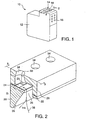
- Fig. 1 is a perspective view of one type of inkjet print cartridge 10 which may incorporate the printhead structures of the present invention.
- the print cartridge 10 of Fig. 1 is the type that contains a substantial quantity of ink within its body 12, but another suitable print cartridge may be the type that receives ink from an external ink supply either mounted on the printhead or connected to the printhead via a tube.
- the ink is supplied to a printhead 14.
- Printhead 14 to be described in detail later, channels the ink into ink ejection chambers, each chamber containing an ink ejection element. Electrical signals are provided to contacts 16 to individually energize the ink ejection elements to eject a droplet of ink through an associated nozzle 18.
- the structure and operation of conventional print cartridges are very well known.
- Fig. 2 is a cross-sectional view of a portion of the printhead of Fig. 1 taken along line 2-2 in Fig. 1.
- a printhead may have 300 or more nozzles and associated ink ejection chambers, detail of only a single ink ejection chamber need be described in order to understand the invention. It should also be understood by those skilled in the art that many printheads are formed on a single silicon wafer and then separated from one another using conventional techniques.
- a silicon substrate 20 has formed on it various thin film layers 22, to be described in detail later.
- the thin film layers 22 include a resistive layer for forming resistors 24.
- Other thin film layers perform various functions, such as providing electrical insulation from the substrate 20, providing a thermally conductive path from the heater resistor elements to the substrate 20, and providing electrical conductors to the resistor elements.
- One electrical conductor 25 is shown leading to one end of a resistor 24.
- a similar conductor leads to the other end of the resistor 24.
- the resistors and conductors in a chamber would be obscured by overlying layers.
- Ink feed holes 26 are formed completely through the thin film layers 22. Each ink feed hole 26 may be larger or smaller than that shown in Fig. 2. There may be multiple holes per chamber.
- a manifold may be formed in the orifice layer 28 for providing a common ink channel for a row of ink ejection chambers 30.
- An orifice layer 28 is deposited over the surface of the thin film layers 22 and etched to form ink ejection chambers 30, one chamber per resistor 24.
- Nozzles 34 may be formed using conventional photolithographic techniques.
- the silicon substrate 20 is etched to form a trench 36 extending along the length of the row of ink feed holes 26 so that ink 38 from an ink reservoir may enter the ink feed holes 26 for supplying ink to the ink ejection chambers 30.
- a thin film sacrificial layer e.g., polysilicon
- the polysilicon or other sacrificial layer must have an etch rate greater than the lateral etch rate of the silicon wafer for the sacrificial layer to have beneficial properties.
- each printhead is approximately one-half inch long and contains two offset rows of nozzles, each row containing 150 nozzles for a total of 300 nozzles per printhead.
- the printhead can thus print at a single pass resolution of 600 dots per inch (dpi) along the direction of the nozzle rows or print at a greater resolution in multiple passes. Greater resolutions may also be printed along the scan direction of the printhead. Resolutions of 1200 or greater dpi may be obtained using the present invention.
- an electrical signal is provided to heater resistor 24, which vaporizes a portion of the ink to form a bubble within the ink ejection chamber 30.
- the bubble propels an ink droplet through an associated nozzle 34 onto a medium.
- the ink ejection chamber is then refilled by capillary action.
- Fig. 3 is a cross-sectional view along line 3-3 of Fig. 2 showing a single ink ejection chamber 30 and the associated structure of the printhead.
- Fig. 3 shows one embodiment of the individual thin film layers. Layers etched away during the TMAH trench etch and BOE wet etch are shown in ghost outline. Conventional deposition, masking, and etching steps are used unless otherwise noted.
- a silicon substrate 20 with a crystalline orientation of ⁇ 100> is placed in a vacuum chamber.
- the bulk silicon is about 675 microns thick.
- a polysilicon layer 44 (shown in ghost outline), having a thickness of between approximately 0.1 and 0.5 microns, is formed over the top surface of the substrate 20.
- the polysilicon layer 44 is masked and etched to leave polysilicon only in the area where the trench 36 is to be formed.
- Fig. 4 is a top down view of a portion of the fully processed wafer showing the location of the poly mask 45.
- the edges of the polysilicon layer 44 will define the edges of the trench 36. It is important that the edges of the trench not affect the intended size of the ink feed holes 26 leading into the ink ejection chambers 30 because the size of the ink feed holes 26 is carefully calculated to provide a certain fluid resistance for optimum performance of the printhead.
- the process described herein uses the polysilicon layer 44 dimensions to define the trench edges so that the backside trench mask can be misaligned without affecting the final trench dimensions. Since the polysilicon layer 44 can be patterned with high precision with respect to the intended ink feed holes 26, the resulting trench edges can be precisely aligned with the ink feed holes 26.
- the poly mask 45 in Fig. 4 patterns the polysilicon layer 44 to extend over the entire trench area, the polysilicon layer 44 need only reside along the periphery of the trench area (but not extend beyond the trench area) where the ink feed holes are to be formed. Forming the polysilicon over the entire trench area is beneficial because the polysilicon results in a much faster silicon wafer etch rate in the lateral direction.
- a field oxide layer 46 having a thickness of 1.2 microns, is formed over the silicon substrate 20 and polysilicon layer 44 using conventional techniques.
- Other types of oxide layers may be used, such as oxides of nitrogen (NOX).
- a phosphosilicate glass (PSG) layer 48 having a thickness of 0.5 microns, is then deposited over the field oxide layer 46 using conventional techniques.
- a boron PSG or boron TEOS (BTEOS) layer may be used instead of PSG layer 48.
- a mask is formed over the PSG layer 48 using conventional photolithographic techniques.
- the PSG layer 48 is then etched using conventional reactive ion etching (RIE) to pull back the PSG layer 48 from the subsequently formed ink feed hole. This will protect the PSG layer 48 from ink.
- RIE reactive ion etching
- a resistive layer (ultimately forming resistors 24) of, for example, tantalum aluminum (TaAl), having a thickness of 0.1 microns, is then the deposited over the PSG layer 48. Other known resistive layers can also be used.
- a conductive layer 25 (see Fig. 2) of AlCu is then deposited over the TaAl.
- a mask is deposited and patterned using conventional photolithographic techniques, and the conductive layer 25 and the resistive layer are etched using conventional IC fabrication techniques. Another masking and etching step is used to remove the portions of the AlCu over the heater resistors 24, as shown in Fig. 2. The resulting AlCu conductors are outside the field of view of Fig. 3.
- the etching of the conductive layer 25 and resistive layer defines a first resistor dimension (e.g., a width).
- a second resistor dimension (e.g., a length) is defined by etching the conductive layer 25 to cause the resistive portion to be contacted by the conductive traces at two ends.
- This technique of forming resistors and electrical conductors is well known in the art.
- the conductive traces are formed so as to not extend across the middle of the printhead, but run along the edges. Appropriate addressing circuitry and pads are provided on the substrate 20 for providing energizing signals to the resistors 24.
- a silicon nitride layer 56 Over the resistors 24 and conductive layer 25 is formed a silicon nitride layer 56, having a thickness of 0.5 microns. This layer provides insulation and passivation.
- nitride layer 56 Over the nitride layer 56 is formed a silicon carbide layer 58, having a thickness of 0.25 microns, to provide additional insulation and passivation.
- the nitride layer 56 and carbide layer 58 protect the PSG layer 48 from the ink.
- Other dielectric layers may be used instead of nitride and carbide.
- passivation layers are then masked (outside the field of view) and etched using conventional techniques to expose portions of the conductive layer 25 for electrical contact to a subsequent gold conductive layer to provide ground lines.
- a bubble cavitation layer 60 of tantalum (Ta) is then formed over the carbide layer 58.
- Gold (Au) is deposited over the tantalum layer 60 and etched to form the ground lines electrically connected to certain ones of the conductive layer 25 traces. The ground lines terminate in bond pads along edges of the substrate 20.
- the AlCu and gold conductors may be coupled to transistors formed on the substrate surface. Such transistors are described in U.S. Patent No. 5,648,806, previously mentioned.
- a mask is patterned to expose portions of the thin film layers above the FOX and PSG oxide layers 46 and 48 corresponding to the ink feed holes 26.
- the thin film layers overlying the oxide layers 46 and 48 in the ink feed hole areas are then etched. Alternately, multiple masking and etching steps may be used as the various thin film layers are formed. This etch process can be a combination of several types of etches (RIE or wet). The etch through the thin film layers may use conventional IC fabrication techniques.
- Fig. 3 shows the layers 44, 46, and 48 as ghost layers within the ink feed hole areas, since these layers are ultimately etched away.
- the orifice layer 28 is then deposited and formed.
- the orifice layer 28 may be formed of a spun-on epoxy called SU8. Orifice layer 28 may alternatively be laminated or screened on.
- the orifice layer in one embodiment is about 20 microns.
- the ink chambers 30 and nozzles 34 are formed through photolithography.
- a first mask using a half dosage of UV radiation "hardens" the upper surface of the SU8 (a negative photoresist) except in locations where the nozzles 34 are to be formed.
- a second mask using a full UV dosage then exposes the SU8 in those areas where neither nozzles 34 nor ink ejection chambers 30 are to be formed. After these two exposures, the SU8 is developed, and the hardened portions remain but the nozzle portions and the ink ejection chamber portions of the SU8 are removed.
- the backside of the wafer is then masked (by mask 76) using conventional techniques to expose the portion of the backside of the wafer to be subjected to the TMAH trench etch.
- the backside mask 76 may be a FOX hard mask formed using conventional photolithographic techniques.
- the wafer is dipped into the wet TMAH etch, which forms the angled profile.
- the trench width will typically be less than 200 microns, and, in one embodiment, is between 20-60 microns.
- the backside masking may be misaligned by a large margin but still must be within the intended trench area. Such misalignment would normally restrict the area of the ink feed hole and have an adverse effect on the fluid properties of the printhead.
- the use of the polysilicon layer 44 avoids any adverse effects of such misalignment.
- the TMAH after etching through the substrate to the polysilicon layer 44, rapidly etches the polysilicon layer 44, forming a gap between the substrate and the oxide layers 46 and 48. This gap exposes the fast etch planes of the substrate, and the TMAH rapidly etches the substrate so that the edges of the trench align with the polysilicon layer 44 edges.
- the trench 36 in one embodiment, extends the length of a row of ink ejection chambers. Any one of several etch techniques could be used. Examples of appropriate wet etches include ethylene diamine pyrocatecol (EDP), potassium hydroxide (KOH), and TMAH. Any one of these or a combination thereof could be used for this application.
- EDP ethylene diamine pyrocatecol
- KOH potassium hydroxide
- TMAH TMAH
- the wafer is then subjected to a conventional wet buffered oxide etch (BOE).
- BOE wet buffered oxide etch
- the BOE etches away the exposed oxide layers 46 and 48 to complete the ink feed holes 26.
- the BOE etches from both the topside of the oxide layers (from within the ink ejection chambers 30) and the underside of the oxide layers, resulting in a relatively rapid etch.
- no masking is used in the wet etch, since the exposed oxide layers 46 and 48 on the topside and underside of the wafer are already aligned with the ink feed hole areas.
- Fig. 5 is a cross-sectional view of a larger portion of the wafer corresponding to the top down view of Fig. 4.
- the sacrificed polysilicon layer 44 is shown in ghost outline. Any thin film layers beneath the orifice layer 28 are not functional and are not shown.
- the PSG layer 48 has been pulled back and protected by the overlying passivation layers from ink.
- the BOE wet etch to complete the ink feed holes 26 only etches through the field oxide layer 46.
- the resulting wafer is then sawed to form the individual printheads.
- a flexible circuit is used to provide electrical access to the conductors on the printhead.
- the resulting assembly is then affixed to a plastic print cartridge, such as that shown in Fig. 1, and the printhead is sealed with respect to the print cartridge body to prevent ink seepage.
- the trench 36 may extend the length of the printhead or, to improve the mechanical strength of the printhead, only extend a portion of the length of the printhead beneath the ink ejection chambers.
- a passivation layer may be deposited on the substrate 20 if reaction of the substrate with the ink is a concern.
- polysilicon was used as the sacrificial layer, other materials, such as metals, may be used instead.
- One suitable metel is titanium, which can be etched with a hydrogen peroxide HF etch.
- polysilicon is preferable since it is etched using the same TMAH etch used to etch the substrate 20.
- Fig. 6 illustrates one embodiment of an inkjet printer 130 that can incorporate the invention. Numerous other designs of inkjet printers may also be used along with this invention, more detail of an inkjet printer is found in U.S. Patent No. 5,852,459, to Norman Pawlowski et al.
- Inkjet printer 130 includes an input tray 132 containing sheets of paper 134 which are forwarded through a print zone 13 5, using rollers 13 7, for being printed upon. The paper 134 is then forwarded to an output tray 136.
- a moveable carriage 13 8 holds print cartridges 140-143, which respectively print cyan (C), black (K), magenta (M), and yellow (Y) ink.
- inks in replaceable ink cartridges 146 are supplied to their associated print cartridges via flexible ink tubes 148.
- the print cartridges may also be the type that hold a substantial supply of fluid and may be refillable or non-refillable.
- the ink supplies are separate from the printhead portions and are removeably mounted on the printheads in the carriage 13 8.
- the carriage 13 8 is moved along a scan axis by a conventional belt and pulley system and slides along a slide rod 150.
- the carriage is stationery, and an array of stationary print cartridges print on a moving sheet of paper.
- Printing signals from a conventional external computer are processed by printer 130 to generate a bitmap of the dots to be printed.
- the bitmap is then converted into firing signals for the printheads.
- the position of the carriage 138 as it traverses back and forth along the scan axis while printing is determined from an optical encoder strip 152, detected by a photoelectric element on carriage 138, to cause the various ink ejection elements on each print cartridge to be selectively tired at the appropriate time during a carriage scan.
- the printhead may use resistive, piezoelectric, or other types of ink ejection elements.
- the print cartridges in carriage 13 8 scan across a sheet of paper, the swaths printed by the print cartridges overlap. After one or more scans, the sheet of paper 134 is shifted in a direction towards the output tray 136, and the carriage 138 resumes scanning.
- the present invention is equally applicable to alternative printing systems (not shown) that utilize alternative media and/or printhead moving mechanisms, such as those incorporating grit wheel, roll feed, or drum or vacuum belt technology to support and move the print media relative to the printhead assemblies.
- a grit wheel design a grit wheel and pinch roller move the media back and forth along one axis while a carriage carrying one or more printhead assemblies scans past the media along an orthogonal axis.
- a drum printer design the media is mounted to a rotating drum that is rotated along one axis while a carriage carrying one or more printhead assemblies scans past the media along an orthogonal axis. In either the drum or grit wheel designs, the scanning is typically not done in a back and forth manner as is the case for the system depicted in Fig. 13.
- printheads may be formed on a single substrate. Further, an array of printheads may extend across the entire width of a page so that no scanning of the printheads is needed; only the paper is shifted perpendicular to the array.
- Additional print cartridges in the carriage may include other colors or fixers.
Description
- This invention relates to inkjet printers and, more particularly, to a monolithic printhead for an inkjet printer.
- Inkjet printers typically have a printhead mounted on a carriage that scans back and forth across the width of a sheet of paper feeding through the printer. Ink from an ink reservoir, either on-board the carriage or external to the carriage, is fed to ink ejection chambers on the printhead. Each ink ejection chamber contains an ink ejection element, such as a heater resistor or a piezoelectric element, which is independently addressable. Energizing an ink ejection element causes a droplet of ink to be ejected through a nozzle for creating a small dot on the medium. The pattern of dots created forms an image or text.
- Additional information regarding one particular type of printhead and inkjet printer is found in U.S. Patent No. 5,648,806, entitled, "Stable Substrate Structure For A Wide Swath Nozzle Array In A High Resolution Inkjet Printer," by Steven Steinfield et al., assigned to the present assignee.
- European Patent Application EP 1 078 755 A discloses a fully integrated thermal inkjet printhead having multiple ink feed holes per nozzle. Thin film layers including ink ejection elements are formed on a top surface of a silicon substrate. The various layers are etched to provide conductive leads to the ink ejection elements. At least one ink feed hole is formed through the thin film layers for each ink ejection chamber. A trench is etched in the bottom surface of the substrate so that ink can flow into the trench and into each ink ejection chamber through the ink feed holes formed in the thin film layers. An orifice layer is formed on the top surface of the thin film layers to define the nozzles and ink ejection chambers.
- As the resolutions and printing speeds of printheads increase to meet the demanding needs of the consumer market, new printhead manufacturing techniques and structures are required.
- The present invention provides a method for forming a printing device as recited in the appended claims.
- A silicon substrate has formed on its top surface a thin polysilicon layer in the area in which a trench is to be later formed in the substrate. The edges of the polysilicon layer align with the intended placement of ink feed holes leading into ink ejection chambers. Thin film layers, including a resistive layer, are then formed on the top surface of the silicon substrate. The thin film layers include oxide layers formed over the polysilicon layer. The various layers are etched to provide conductive leads to the heater resistor elements. Piezoelectric elements may be used instead of the resistive elements.
- At least one ink feed hole is partially formed through the thin film layers for each ink ejection chamber, leaving the oxide layers over the polysilicon layer in the ink feed hole areas.
- An orifice layer is formed on the top surface of the thin film layers to define the nozzles and ink ejection chambers. In one embodiment, a photo-definable material is used to form the orifice layer.
- A trench mask is formed on the bottom surface of the substrate. A trench is etched (using, for example, TMAH) through the exposed bottom surface of the substrate. When the substrate is etched to the polysilicon layer, the TMAH rapidly etches away the polysilicon sandwiched between the silicon substrate and the oxide layers, creating a gap between the silicon substrate and the oxide layers. This gap exposes fast etch planes of the silicon. Such fast etch planes may be, for example, (110) and others. The TMAH then rapidly etches the silicon substrate along the etch planes, thus aligning the edges of the trench with the polysilicon edges. The lateral (in the plane of the wafer) trench etch rate during this rapid etch has been shown in simulations to be 100 microns or more per hour as compared with the lateral component of purely (111) plane etching, which is usually 2-6 microns per hour. The rapid lateral etch rate is almost twice as fast as the vertical etch rate along the <100> direction.
- A wet etch is then performed using a buffered oxide etch (BOE) solution. The etchant enters the ink chambers through the nozzles and etches the exposed oxide layers in the ink feed hole areas from the topside. The oxide layers exposed by the trench are also etched from the underside during the same wet etching step. Thus, the wet etching, without the use of any masks, quickly etches the exposed oxide layers from the topside and underside. The BOE will completely etch through the exposed oxide layers forming ink feed holes through the thin film layers. The trench is aligned with the ink feed holes due to the polysilicon layer.
- This process allows some misalignment of the trench mask without affecting the final trench dimensions.
- The resulting fully integrated thermal inkjet printhead can be manufactured to a very precise tolerance since the entire structure is monolithic, meeting the needs for the next generation of printheads.
- The process may be used to form openings in devices other than printheads.
-
- Fig. 1 is a perspective view of one embodiment of a print cartridge that may incorporate the printheads described herein.
- Fig. 2 is a perspective cutaway view of a portion of one embodiment of a printhead in accordance with the present invention.
- Fig. 3 is a cross-sectional view of the printhead portion of Fig. 2 along line 3-3 showing additional detail of the thin film layers.
- Fig. 4 is a top down partially transparent view of the printhead shown in Fig. 2, showing additional portions of the printhead.
- Fig. 5 is a cross-sectional view along line 3-3 in Fig. 2 showing additional portions of the printhead.
- Fig. 6 is a perspective view of a conventional inkjet printer into which the printheads of the present invention may be installed for printing on a medium.
-
- Fig. 1 is a perspective view of one type of
inkjet print cartridge 10 which may incorporate the printhead structures of the present invention. Theprint cartridge 10 of Fig. 1 is the type that contains a substantial quantity of ink within itsbody 12, but another suitable print cartridge may be the type that receives ink from an external ink supply either mounted on the printhead or connected to the printhead via a tube. - The ink is supplied to a
printhead 14.Printhead 14, to be described in detail later, channels the ink into ink ejection chambers, each chamber containing an ink ejection element. Electrical signals are provided tocontacts 16 to individually energize the ink ejection elements to eject a droplet of ink through an associatednozzle 18. The structure and operation of conventional print cartridges are very well known. - Fig. 2 is a cross-sectional view of a portion of the printhead of Fig. 1 taken along line 2-2 in Fig. 1. Although a printhead may have 300 or more nozzles and associated ink ejection chambers, detail of only a single ink ejection chamber need be described in order to understand the invention. It should also be understood by those skilled in the art that many printheads are formed on a single silicon wafer and then separated from one another using conventional techniques.
- In Fig. 2, a
silicon substrate 20 has formed on it variousthin film layers 22, to be described in detail later. Thethin film layers 22 include a resistive layer for formingresistors 24. Other thin film layers perform various functions, such as providing electrical insulation from thesubstrate 20, providing a thermally conductive path from the heater resistor elements to thesubstrate 20, and providing electrical conductors to the resistor elements. Oneelectrical conductor 25 is shown leading to one end of aresistor 24. A similar conductor leads to the other end of theresistor 24. In an actual embodiment, the resistors and conductors in a chamber would be obscured by overlying layers. - Ink feed holes 26 are formed completely through the thin film layers 22. Each
ink feed hole 26 may be larger or smaller than that shown in Fig. 2. There may be multiple holes per chamber. A manifold may be formed in theorifice layer 28 for providing a common ink channel for a row ofink ejection chambers 30. - An
orifice layer 28 is deposited over the surface of the thin film layers 22 and etched to formink ejection chambers 30, one chamber perresistor 24.Nozzles 34 may be formed using conventional photolithographic techniques. - The
silicon substrate 20 is etched to form atrench 36 extending along the length of the row of ink feed holes 26 so thatink 38 from an ink reservoir may enter the ink feed holes 26 for supplying ink to theink ejection chambers 30. A thin film sacrificial layer (e.g., polysilicon), described below, is used to precisely align the edges of thetrench 36 with the ink feed holes 26. The polysilicon or other sacrificial layer must have an etch rate greater than the lateral etch rate of the silicon wafer for the sacrificial layer to have beneficial properties. - In one embodiment, each printhead is approximately one-half inch long and contains two offset rows of nozzles, each row containing 150 nozzles for a total of 300 nozzles per printhead. The printhead can thus print at a single pass resolution of 600 dots per inch (dpi) along the direction of the nozzle rows or print at a greater resolution in multiple passes. Greater resolutions may also be printed along the scan direction of the printhead. Resolutions of 1200 or greater dpi may be obtained using the present invention.
- In operation, an electrical signal is provided to
heater resistor 24, which vaporizes a portion of the ink to form a bubble within theink ejection chamber 30. The bubble propels an ink droplet through an associatednozzle 34 onto a medium. The ink ejection chamber is then refilled by capillary action. - Fig. 3 is a cross-sectional view along line 3-3 of Fig. 2 showing a single
ink ejection chamber 30 and the associated structure of the printhead. Fig. 3 shows one embodiment of the individual thin film layers. Layers etched away during the TMAH trench etch and BOE wet etch are shown in ghost outline. Conventional deposition, masking, and etching steps are used unless otherwise noted. - To form the structure of Fig. 3, a
silicon substrate 20 with a crystalline orientation of <100> is placed in a vacuum chamber. The bulk silicon is about 675 microns thick. - A polysilicon layer 44 (shown in ghost outline), having a thickness of between approximately 0.1 and 0.5 microns, is formed over the top surface of the
substrate 20. Thepolysilicon layer 44 is masked and etched to leave polysilicon only in the area where thetrench 36 is to be formed. Fig. 4 is a top down view of a portion of the fully processed wafer showing the location of thepoly mask 45. The edges of thepolysilicon layer 44 will define the edges of thetrench 36. It is important that the edges of the trench not affect the intended size of the ink feed holes 26 leading into theink ejection chambers 30 because the size of the ink feed holes 26 is carefully calculated to provide a certain fluid resistance for optimum performance of the printhead. It is difficult to obtain repeatable trench dimensions by only using a backside trench mask followed by a TMAH etch of the substrate. The process described herein uses thepolysilicon layer 44 dimensions to define the trench edges so that the backside trench mask can be misaligned without affecting the final trench dimensions. Since thepolysilicon layer 44 can be patterned with high precision with respect to the intended ink feed holes 26, the resulting trench edges can be precisely aligned with the ink feed holes 26. - Although the
poly mask 45 in Fig. 4 patterns thepolysilicon layer 44 to extend over the entire trench area, thepolysilicon layer 44 need only reside along the periphery of the trench area (but not extend beyond the trench area) where the ink feed holes are to be formed. Forming the polysilicon over the entire trench area is beneficial because the polysilicon results in a much faster silicon wafer etch rate in the lateral direction. - Referring back to Fig. 3, a
field oxide layer 46, having a thickness of 1.2 microns, is formed over thesilicon substrate 20 andpolysilicon layer 44 using conventional techniques. Other types of oxide layers may be used, such as oxides of nitrogen (NOX). A phosphosilicate glass (PSG)layer 48, having a thickness of 0.5 microns, is then deposited over thefield oxide layer 46 using conventional techniques. A boron PSG or boron TEOS (BTEOS) layer may be used instead ofPSG layer 48. - In an alternative embodiment, a mask is formed over the
PSG layer 48 using conventional photolithographic techniques. ThePSG layer 48 is then etched using conventional reactive ion etching (RIE) to pull back thePSG layer 48 from the subsequently formed ink feed hole. This will protect thePSG layer 48 from ink. In such an embodiment, the PSG does not extend over the ink feed hole areas. Such an embodiment is shown in Fig. 5. - A resistive layer (ultimately forming resistors 24) of, for example, tantalum aluminum (TaAl), having a thickness of 0.1 microns, is then the deposited over the
PSG layer 48. Other known resistive layers can also be used. A conductive layer 25 (see Fig. 2) of AlCu is then deposited over the TaAl. A mask is deposited and patterned using conventional photolithographic techniques, and theconductive layer 25 and the resistive layer are etched using conventional IC fabrication techniques. Another masking and etching step is used to remove the portions of the AlCu over theheater resistors 24, as shown in Fig. 2. The resulting AlCu conductors are outside the field of view of Fig. 3. - The etching of the
conductive layer 25 and resistive layer defines a first resistor dimension (e.g., a width). A second resistor dimension (e.g., a length) is defined by etching theconductive layer 25 to cause the resistive portion to be contacted by the conductive traces at two ends. This technique of forming resistors and electrical conductors is well known in the art. The conductive traces are formed so as to not extend across the middle of the printhead, but run along the edges. Appropriate addressing circuitry and pads are provided on thesubstrate 20 for providing energizing signals to theresistors 24. - Over the
resistors 24 andconductive layer 25 is formed asilicon nitride layer 56, having a thickness of 0.5 microns. This layer provides insulation and passivation. - Over the
nitride layer 56 is formed asilicon carbide layer 58, having a thickness of 0.25 microns, to provide additional insulation and passivation. Thenitride layer 56 andcarbide layer 58 protect thePSG layer 48 from the ink. Other dielectric layers may be used instead of nitride and carbide. - The passivation layers are then masked (outside the field of view) and etched using conventional techniques to expose portions of the
conductive layer 25 for electrical contact to a subsequent gold conductive layer to provide ground lines. - A
bubble cavitation layer 60 of tantalum (Ta) is then formed over thecarbide layer 58. Gold (Au), not shown, is deposited over thetantalum layer 60 and etched to form the ground lines electrically connected to certain ones of theconductive layer 25 traces. The ground lines terminate in bond pads along edges of thesubstrate 20. - The AlCu and gold conductors may be coupled to transistors formed on the substrate surface. Such transistors are described in U.S. Patent No. 5,648,806, previously mentioned.
- A mask is patterned to expose portions of the thin film layers above the FOX and PSG oxide layers 46 and 48 corresponding to the ink feed holes 26. The thin film layers overlying the oxide layers 46 and 48 in the ink feed hole areas are then etched. Alternately, multiple masking and etching steps may be used as the various thin film layers are formed. This etch process can be a combination of several types of etches (RIE or wet). The etch through the thin film layers may use conventional IC fabrication techniques.
- Fig. 3 shows the
layers - An
orifice layer 28 is then deposited and formed. Theorifice layer 28 may be formed of a spun-on epoxy called SU8.Orifice layer 28 may alternatively be laminated or screened on. The orifice layer in one embodiment is about 20 microns. Theink chambers 30 andnozzles 34 are formed through photolithography. In one technique, a first mask using a half dosage of UV radiation "hardens" the upper surface of the SU8 (a negative photoresist) except in locations where thenozzles 34 are to be formed. A second mask using a full UV dosage then exposes the SU8 in those areas where neithernozzles 34 norink ejection chambers 30 are to be formed. After these two exposures, the SU8 is developed, and the hardened portions remain but the nozzle portions and the ink ejection chamber portions of the SU8 are removed. - The backside of the wafer is then masked (by mask 76) using conventional techniques to expose the portion of the backside of the wafer to be subjected to the TMAH trench etch. The
backside mask 76 may be a FOX hard mask formed using conventional photolithographic techniques. The wafer is dipped into the wet TMAH etch, which forms the angled profile. The trench width will typically be less than 200 microns, and, in one embodiment, is between 20-60 microns. The backside masking may be misaligned by a large margin but still must be within the intended trench area. Such misalignment would normally restrict the area of the ink feed hole and have an adverse effect on the fluid properties of the printhead. However, the use of thepolysilicon layer 44 avoids any adverse effects of such misalignment. The TMAH, after etching through the substrate to thepolysilicon layer 44, rapidly etches thepolysilicon layer 44, forming a gap between the substrate and the oxide layers 46 and 48. This gap exposes the fast etch planes of the substrate, and the TMAH rapidly etches the substrate so that the edges of the trench align with thepolysilicon layer 44 edges. - The
trench 36, in one embodiment, extends the length of a row of ink ejection chambers. Any one of several etch techniques could be used. Examples of appropriate wet etches include ethylene diamine pyrocatecol (EDP), potassium hydroxide (KOH), and TMAH. Any one of these or a combination thereof could be used for this application. - The wafer is then subjected to a conventional wet buffered oxide etch (BOE). The BOE etches away the exposed
oxide layers oxide layers - Fig. 5 is a cross-sectional view of a larger portion of the wafer corresponding to the top down view of Fig. 4. The sacrificed
polysilicon layer 44 is shown in ghost outline. Any thin film layers beneath theorifice layer 28 are not functional and are not shown. - In the embodiment of Fig. 5, the
PSG layer 48 has been pulled back and protected by the overlying passivation layers from ink. Thus, in the embodiment of Fig. 5, the BOE wet etch to complete the ink feed holes 26 only etches through thefield oxide layer 46. - The resulting wafer is then sawed to form the individual printheads. A flexible circuit is used to provide electrical access to the conductors on the printhead. The resulting assembly is then affixed to a plastic print cartridge, such as that shown in Fig. 1, and the printhead is sealed with respect to the print cartridge body to prevent ink seepage.
- Additional details of forming thin film layers may be found in U.S. Patent No.6,336,714 , entitled "Fully Integrated Thermal Inkjet Printhead Having Thin Film Layer Shelf," filed August 27, 1999, by Naoto Kawamura et al., assigned to the present assignee.
- The
trench 36 may extend the length of the printhead or, to improve the mechanical strength of the printhead, only extend a portion of the length of the printhead beneath the ink ejection chambers. A passivation layer may be deposited on thesubstrate 20 if reaction of the substrate with the ink is a concern. - Although polysilicon was used as the sacrificial layer, other materials, such as metals, may be used instead. One suitable metel is titanium, which can be etched with a hydrogen peroxide HF etch. However, polysilicon is preferable since it is etched using the same TMAH etch used to etch the
substrate 20. - One skilled in the art of integrated circuit manufacturing would understand the various techniques used to form the printhead structures described herein. The thin film layers and their thicknesses may be varied, and some layers deleted, while still obtaining the benefits of the present invention. Additional ink feed hole patterns are also envisioned.
- Fig. 6 illustrates one embodiment of an
inkjet printer 130 that can incorporate the invention. Numerous other designs of inkjet printers may also be used along with this invention, more detail of an inkjet printer is found in U.S. Patent No. 5,852,459, to Norman Pawlowski et al. -
Inkjet printer 130 includes aninput tray 132 containing sheets ofpaper 134 which are forwarded through a print zone 13 5, using rollers 13 7, for being printed upon. Thepaper 134 is then forwarded to anoutput tray 136. A moveable carriage 13 8 holds print cartridges 140-143, which respectively print cyan (C), black (K), magenta (M), and yellow (Y) ink. - In one embodiment, inks in
replaceable ink cartridges 146 are supplied to their associated print cartridges viaflexible ink tubes 148. The print cartridges may also be the type that hold a substantial supply of fluid and may be refillable or non-refillable. In another embodiment, the ink supplies are separate from the printhead portions and are removeably mounted on the printheads in the carriage 13 8. - The carriage 13 8 is moved along a scan axis by a conventional belt and pulley system and slides along a
slide rod 150. In another embodiment, the carriage is stationery, and an array of stationary print cartridges print on a moving sheet of paper. - Printing signals from a conventional external computer (e.g., a PC) are processed by
printer 130 to generate a bitmap of the dots to be printed. The bitmap is then converted into firing signals for the printheads. The position of thecarriage 138 as it traverses back and forth along the scan axis while printing is determined from anoptical encoder strip 152, detected by a photoelectric element oncarriage 138, to cause the various ink ejection elements on each print cartridge to be selectively tired at the appropriate time during a carriage scan. - The printhead may use resistive, piezoelectric, or other types of ink ejection elements.
- As the print cartridges in carriage 13 8 scan across a sheet of paper, the swaths printed by the print cartridges overlap. After one or more scans, the sheet of
paper 134 is shifted in a direction towards theoutput tray 136, and thecarriage 138 resumes scanning. - The present invention is equally applicable to alternative printing systems (not shown) that utilize alternative media and/or printhead moving mechanisms, such as those incorporating grit wheel, roll feed, or drum or vacuum belt technology to support and move the print media relative to the printhead assemblies. With a grit wheel design, a grit wheel and pinch roller move the media back and forth along one axis while a carriage carrying one or more printhead assemblies scans past the media along an orthogonal axis. With a drum printer design, the media is mounted to a rotating drum that is rotated along one axis while a carriage carrying one or more printhead assemblies scans past the media along an orthogonal axis. In either the drum or grit wheel designs, the scanning is typically not done in a back and forth manner as is the case for the system depicted in Fig. 13.
- Multiple printheads may be formed on a single substrate. Further, an array of printheads may extend across the entire width of a page so that no scanning of the printheads is needed; only the paper is shifted perpendicular to the array.
- Additional print cartridges in the carriage may include other colors or fixers.
Claims (11)
- A method for forming a printing device comprising:providing a printhead substrate (20);forming a polysilicon layer (44) over a first surface of said substrate, said polysilicon layer having peripheral portions for defining edges of a trench (36) to be subsequently formed in said substrate, said peripheral portions being aligned with an intended boundary of ink feed holes (26), to be later formed;forming a plurality of thin film layers (46, 48)on said first surface of said substrate, at least one of said layers forming a plurality of ink ejection elements (24);forming ink feed openings (26) through at least some of said thin film layers;forming an orifice layer (20) over said thin film layers, said orifice layer defining a plurality of ink ejection chambers (30), each chamber having within it an ink ejection element, said orifice layer further defining a nozzle (34) for each ink ejection chamber;masking a second surface of said substrate to perform a trench etch;etching said second surface of said substrate using a wet etchant to form a trench, said etching also etching said polysilicon layer, said trench having at least some edges aligned with said peripheral portions of said polysilicon layer; andwet etching portions of said thin film layers exposed through said ink feed openings and by said trench to self-align edges of said trench substantially to said ink feed holes formed completely through said thin film layers.
- The method of Claim 1 wherein said thin film layers include one or more oxide layers (46, 48), said wet etching etching away portions of said one or more oxide layers to form said ink feed holes (26).
- The method of Claim 2 wherein said oxide layers comprises a field oxide layer (46).
- The method of Claim 2 wherein said oxide layers comprise a PSG layer (48).
- The method of Claim 2 wherein said oxide layers comprise a NOX layer.
- The method of Claim 1 wherein said orifice layer (28) at least partially defines boundaries of said ink feed holes (26).
- The method of Claim 1 wherein said etching said second surface of said substrate to form a trench (36) comprises etching said substrate (20) with a TMAH solution to form an angled trench edge with respect to said second surface.
- The method of Claim 1 wherein said wet etching uses a buffered oxide etch.
- The method of Claim 1 wherein said wet etching is performed without a mask.
- The method of Claim 1 wherein said printhead substrate is part of a semiconductor wafer, said method further comprising:separating out printheads from said wafer; andinstalling said printheads in print cartridges (10).
- The method of Claim 10 further comprising installing said print cartridges (10) in inkjet printers (130).
Applications Claiming Priority (2)
| Application Number | Priority Date | Filing Date | Title |
|---|---|---|---|
| US811052 | 2001-03-15 | ||
| US09/811,052 US6517735B2 (en) | 2001-03-15 | 2001-03-15 | Ink feed trench etch technique for a fully integrated thermal inkjet printhead |
Publications (3)
| Publication Number | Publication Date |
|---|---|
| EP1241009A2 EP1241009A2 (en) | 2002-09-18 |
| EP1241009A3 EP1241009A3 (en) | 2003-07-02 |
| EP1241009B1 true EP1241009B1 (en) | 2005-05-25 |
Family
ID=25205411
Family Applications (1)
| Application Number | Title | Priority Date | Filing Date |
|---|---|---|---|
| EP02251654A Expired - Fee Related EP1241009B1 (en) | 2001-03-15 | 2002-03-08 | Ink feed trench etch technique for a fully integrated thermal inkjet printhead |
Country Status (5)
| Country | Link |
|---|---|
| US (1) | US6517735B2 (en) |
| EP (1) | EP1241009B1 (en) |
| JP (1) | JP4278335B2 (en) |
| DE (1) | DE60204251T2 (en) |
| HK (1) | HK1046388B (en) |
Cited By (4)
| Publication number | Priority date | Publication date | Assignee | Title |
|---|---|---|---|---|
| US7988247B2 (en) | 2007-01-11 | 2011-08-02 | Fujifilm Dimatix, Inc. | Ejection of drops having variable drop size from an ink jet printer |
| US8459768B2 (en) | 2004-03-15 | 2013-06-11 | Fujifilm Dimatix, Inc. | High frequency droplet ejection device and method |
| US8491076B2 (en) | 2004-03-15 | 2013-07-23 | Fujifilm Dimatix, Inc. | Fluid droplet ejection devices and methods |
| US8708441B2 (en) | 2004-12-30 | 2014-04-29 | Fujifilm Dimatix, Inc. | Ink jet printing |
Families Citing this family (11)
| Publication number | Priority date | Publication date | Assignee | Title |
|---|---|---|---|---|
| US6675476B2 (en) * | 2000-12-05 | 2004-01-13 | Hewlett-Packard Development Company, L.P. | Slotted substrates and techniques for forming same |
| US7052117B2 (en) | 2002-07-03 | 2006-05-30 | Dimatix, Inc. | Printhead having a thin pre-fired piezoelectric layer |
| KR100499132B1 (en) * | 2002-10-24 | 2005-07-04 | 삼성전자주식회사 | Inkjet printhead and manufacturing method thereof |
| CN100355573C (en) * | 2002-12-27 | 2007-12-19 | 佳能株式会社 | Ink-jet recording head and mfg. method, and substrate for mfg. ink-jet recording head |
| US7036913B2 (en) * | 2003-05-27 | 2006-05-02 | Samsung Electronics Co., Ltd. | Ink-jet printhead |
| JP4854328B2 (en) * | 2005-04-13 | 2012-01-18 | キヤノン株式会社 | Liquid discharge recording head |
| US7390745B2 (en) | 2005-09-23 | 2008-06-24 | International Business Machines Corporation | Pattern enhancement by crystallographic etching |
| US9016837B2 (en) | 2013-05-14 | 2015-04-28 | Stmicroelectronics, Inc. | Ink jet printhead device with compressive stressed dielectric layer |
| US9016836B2 (en) * | 2013-05-14 | 2015-04-28 | Stmicroelectronics, Inc. | Ink jet printhead with polarity-changing driver for thermal resistors |
| US11746005B2 (en) * | 2021-03-04 | 2023-09-05 | Funai Electric Co. Ltd | Deep reactive ion etching process for fluid ejection heads |
| CN113584456A (en) * | 2021-07-21 | 2021-11-02 | 深圳清华大学研究院 | Ultra-smooth framework and processing method thereof |
Family Cites Families (11)
| Publication number | Priority date | Publication date | Assignee | Title |
|---|---|---|---|---|
| JP2635043B2 (en) | 1986-04-28 | 1997-07-30 | ヒューレット・パッカード・カンパニー | Thermal ink jet print head |
| US4789425A (en) | 1987-08-06 | 1988-12-06 | Xerox Corporation | Thermal ink jet printhead fabricating process |
| US4864329A (en) | 1988-09-22 | 1989-09-05 | Xerox Corporation | Fluid handling device with filter and fabrication process therefor |
| US5001085A (en) * | 1990-07-17 | 1991-03-19 | Micron Technology, Inc. | Process for creating a metal etch mask which may be utilized for halogen-plasma excavation of deep trenches |
| US5648806A (en) | 1992-04-02 | 1997-07-15 | Hewlett-Packard Company | Stable substrate structure for a wide swath nozzle array in a high resolution inkjet printer |
| US5852459A (en) | 1994-10-31 | 1998-12-22 | Hewlett-Packard Company | Printer using print cartridge with internal pressure regulator |
| US6305790B1 (en) * | 1996-02-07 | 2001-10-23 | Hewlett-Packard Company | Fully integrated thermal inkjet printhead having multiple ink feed holes per nozzle |
| DE69730667T2 (en) | 1996-11-11 | 2005-09-22 | Canon K.K. | A method of making a via, use of this method of making a silicon substrate having such a via, or apparatus with that substrate, methods of making an inkjet printhead, and use of this method of making an inkjet printhead |
| US6019907A (en) * | 1997-08-08 | 2000-02-01 | Hewlett-Packard Company | Forming refill for monolithic inkjet printhead |
| US6154234A (en) * | 1998-01-09 | 2000-11-28 | Hewlett-Packard Company | Monolithic ink jet nozzle formed from an oxide and nitride composition |
| US6391527B2 (en) * | 1998-04-16 | 2002-05-21 | Canon Kabushiki Kaisha | Method of producing micro structure, method of production liquid discharge head |
-
2001
- 2001-03-15 US US09/811,052 patent/US6517735B2/en not_active Expired - Fee Related
-
2002
- 2002-03-08 DE DE60204251T patent/DE60204251T2/en not_active Expired - Lifetime
- 2002-03-08 EP EP02251654A patent/EP1241009B1/en not_active Expired - Fee Related
- 2002-03-15 JP JP2002071598A patent/JP4278335B2/en not_active Expired - Fee Related
- 2002-10-29 HK HK02107817.4A patent/HK1046388B/en not_active IP Right Cessation
Cited By (4)
| Publication number | Priority date | Publication date | Assignee | Title |
|---|---|---|---|---|
| US8459768B2 (en) | 2004-03-15 | 2013-06-11 | Fujifilm Dimatix, Inc. | High frequency droplet ejection device and method |
| US8491076B2 (en) | 2004-03-15 | 2013-07-23 | Fujifilm Dimatix, Inc. | Fluid droplet ejection devices and methods |
| US8708441B2 (en) | 2004-12-30 | 2014-04-29 | Fujifilm Dimatix, Inc. | Ink jet printing |
| US7988247B2 (en) | 2007-01-11 | 2011-08-02 | Fujifilm Dimatix, Inc. | Ejection of drops having variable drop size from an ink jet printer |
Also Published As
| Publication number | Publication date |
|---|---|
| US20020129495A1 (en) | 2002-09-19 |
| DE60204251D1 (en) | 2005-06-30 |
| US6517735B2 (en) | 2003-02-11 |
| JP2002283580A (en) | 2002-10-03 |
| EP1241009A3 (en) | 2003-07-02 |
| HK1046388A1 (en) | 2003-01-10 |
| HK1046388B (en) | 2005-09-23 |
| JP4278335B2 (en) | 2009-06-10 |
| EP1241009A2 (en) | 2002-09-18 |
| DE60204251T2 (en) | 2006-05-11 |
Similar Documents
| Publication | Publication Date | Title |
|---|---|---|
| US6419346B1 (en) | Two-step trench etch for a fully integrated thermal inkjet printhead | |
| EP1078755B1 (en) | Fully integrated thermal inkjet printhead having multiple ink feed holes per nozzle | |
| US6938340B2 (en) | Method of forming a printhead using a silicon on insulator substrate | |
| EP1078754B1 (en) | Fully integrated thermal inkjet printhead having etched back phosphosilicate glass layer | |
| EP1078753B1 (en) | Fully integrated thermal inkjet printhead having thin film layer shelf | |
| EP1241009B1 (en) | Ink feed trench etch technique for a fully integrated thermal inkjet printhead | |
| EP1308283B1 (en) | Printhead having a thin film membrane with a floating section | |
| EP1211076B1 (en) | Ink-feed channel structure for fully integrated ink-jet printhead | |
| US6234623B1 (en) | Integral ink filter for ink jet printhead | |
| US6782621B2 (en) | Method of fabricating a fluid ejector |
Legal Events
| Date | Code | Title | Description |
|---|---|---|---|
| PUAI | Public reference made under article 153(3) epc to a published international application that has entered the european phase |
Free format text: ORIGINAL CODE: 0009012 |
|
| AK | Designated contracting states |
Kind code of ref document: A2 Designated state(s): AT BE CH CY DE DK ES FI FR GB GR IE IT LI LU MC NL PT SE TR |
|
| AX | Request for extension of the european patent |
Free format text: AL;LT;LV;MK;RO;SI |
|
| PUAL | Search report despatched |
Free format text: ORIGINAL CODE: 0009013 |
|
| AK | Designated contracting states |
Designated state(s): AT BE CH CY DE DK ES FI FR GB GR IE IT LI LU MC NL PT SE TR |
|
| AX | Request for extension of the european patent |
Extension state: AL LT LV MK RO SI |
|
| 17P | Request for examination filed |
Effective date: 20030811 |
|
| 17Q | First examination report despatched |
Effective date: 20040204 |
|
| AKX | Designation fees paid |
Designated state(s): DE FR GB NL |
|
| GRAP | Despatch of communication of intention to grant a patent |
Free format text: ORIGINAL CODE: EPIDOSNIGR1 |
|
| GRAS | Grant fee paid |
Free format text: ORIGINAL CODE: EPIDOSNIGR3 |
|
| GRAA | (expected) grant |
Free format text: ORIGINAL CODE: 0009210 |
|
| AK | Designated contracting states |
Kind code of ref document: B1 Designated state(s): DE FR GB NL |
|
| REG | Reference to a national code |
Ref country code: GB Ref legal event code: FG4D |
|
| REG | Reference to a national code |
Ref country code: IE Ref legal event code: FG4D |
|
| REF | Corresponds to: |
Ref document number: 60204251 Country of ref document: DE Date of ref document: 20050630 Kind code of ref document: P |
|
| REG | Reference to a national code |
Ref country code: HK Ref legal event code: GR Ref document number: 1046388 Country of ref document: HK |
|
| PLBE | No opposition filed within time limit |
Free format text: ORIGINAL CODE: 0009261 |
|
| STAA | Information on the status of an ep patent application or granted ep patent |
Free format text: STATUS: NO OPPOSITION FILED WITHIN TIME LIMIT |
|
| ET | Fr: translation filed | ||
| 26N | No opposition filed |
Effective date: 20060228 |
|
| REG | Reference to a national code |
Ref country code: GB Ref legal event code: 732E Free format text: REGISTERED BETWEEN 20120329 AND 20120404 |
|
| REG | Reference to a national code |
Ref country code: NL Ref legal event code: SD Effective date: 20120731 |
|
| PGFP | Annual fee paid to national office [announced via postgrant information from national office to epo] |
Ref country code: GB Payment date: 20130228 Year of fee payment: 12 Ref country code: DE Payment date: 20130221 Year of fee payment: 12 |
|
| PGFP | Annual fee paid to national office [announced via postgrant information from national office to epo] |
Ref country code: NL Payment date: 20130222 Year of fee payment: 12 |
|
| PGFP | Annual fee paid to national office [announced via postgrant information from national office to epo] |
Ref country code: FR Payment date: 20130429 Year of fee payment: 12 |
|
| REG | Reference to a national code |
Ref country code: DE Ref legal event code: R119 Ref document number: 60204251 Country of ref document: DE |
|
| REG | Reference to a national code |
Ref country code: NL Ref legal event code: V1 Effective date: 20141001 |
|
| GBPC | Gb: european patent ceased through non-payment of renewal fee |
Effective date: 20140308 |
|
| REG | Reference to a national code |
Ref country code: FR Ref legal event code: ST Effective date: 20141128 |
|
| REG | Reference to a national code |
Ref country code: DE Ref legal event code: R119 Ref document number: 60204251 Country of ref document: DE Effective date: 20141001 |
|
| PG25 | Lapsed in a contracting state [announced via postgrant information from national office to epo] |
Ref country code: FR Free format text: LAPSE BECAUSE OF NON-PAYMENT OF DUE FEES Effective date: 20140331 Ref country code: DE Free format text: LAPSE BECAUSE OF NON-PAYMENT OF DUE FEES Effective date: 20141001 Ref country code: GB Free format text: LAPSE BECAUSE OF NON-PAYMENT OF DUE FEES Effective date: 20140308 |
|
| PG25 | Lapsed in a contracting state [announced via postgrant information from national office to epo] |
Ref country code: NL Free format text: LAPSE BECAUSE OF NON-PAYMENT OF DUE FEES Effective date: 20141001 |