EP1237242A1 - Quantum cascade laser with relaxation-stabilized injection - Google Patents
Quantum cascade laser with relaxation-stabilized injection Download PDFInfo
- Publication number
- EP1237242A1 EP1237242A1 EP02251369A EP02251369A EP1237242A1 EP 1237242 A1 EP1237242 A1 EP 1237242A1 EP 02251369 A EP02251369 A EP 02251369A EP 02251369 A EP02251369 A EP 02251369A EP 1237242 A1 EP1237242 A1 EP 1237242A1
- Authority
- EP
- European Patent Office
- Prior art keywords
- miniband
- minibands
- charge carriers
- active
- layers
- Prior art date
- Legal status (The legal status is an assumption and is not a legal conclusion. Google has not performed a legal analysis and makes no representation as to the accuracy of the status listed.)
- Withdrawn
Links
Images

Classifications
-
- B—PERFORMING OPERATIONS; TRANSPORTING
- B82—NANOTECHNOLOGY
- B82Y—SPECIFIC USES OR APPLICATIONS OF NANOSTRUCTURES; MEASUREMENT OR ANALYSIS OF NANOSTRUCTURES; MANUFACTURE OR TREATMENT OF NANOSTRUCTURES
- B82Y20/00—Nanooptics, e.g. quantum optics or photonic crystals
-
- H—ELECTRICITY
- H01—ELECTRIC ELEMENTS
- H01S—DEVICES USING THE PROCESS OF LIGHT AMPLIFICATION BY STIMULATED EMISSION OF RADIATION [LASER] TO AMPLIFY OR GENERATE LIGHT; DEVICES USING STIMULATED EMISSION OF ELECTROMAGNETIC RADIATION IN WAVE RANGES OTHER THAN OPTICAL
- H01S5/00—Semiconductor lasers
- H01S5/30—Structure or shape of the active region; Materials used for the active region
- H01S5/34—Structure or shape of the active region; Materials used for the active region comprising quantum well or superlattice structures, e.g. single quantum well [SQW] lasers, multiple quantum well [MQW] lasers or graded index separate confinement heterostructure [GRINSCH] lasers
- H01S5/3401—Structure or shape of the active region; Materials used for the active region comprising quantum well or superlattice structures, e.g. single quantum well [SQW] lasers, multiple quantum well [MQW] lasers or graded index separate confinement heterostructure [GRINSCH] lasers having no PN junction, e.g. unipolar lasers, intersubband lasers, quantum cascade lasers
- H01S5/3402—Structure or shape of the active region; Materials used for the active region comprising quantum well or superlattice structures, e.g. single quantum well [SQW] lasers, multiple quantum well [MQW] lasers or graded index separate confinement heterostructure [GRINSCH] lasers having no PN junction, e.g. unipolar lasers, intersubband lasers, quantum cascade lasers intersubband lasers, e.g. transitions within the conduction or valence bands
-
- H—ELECTRICITY
- H01—ELECTRIC ELEMENTS
- H01S—DEVICES USING THE PROCESS OF LIGHT AMPLIFICATION BY STIMULATED EMISSION OF RADIATION [LASER] TO AMPLIFY OR GENERATE LIGHT; DEVICES USING STIMULATED EMISSION OF ELECTROMAGNETIC RADIATION IN WAVE RANGES OTHER THAN OPTICAL
- H01S5/00—Semiconductor lasers
- H01S5/06—Arrangements for controlling the laser output parameters, e.g. by operating on the active medium
- H01S5/062—Arrangements for controlling the laser output parameters, e.g. by operating on the active medium by varying the potential of the electrodes
- H01S5/0625—Arrangements for controlling the laser output parameters, e.g. by operating on the active medium by varying the potential of the electrodes in multi-section lasers
- H01S5/06255—Controlling the frequency of the radiation
- H01S5/06256—Controlling the frequency of the radiation with DBR-structure
-
- H—ELECTRICITY
- H01—ELECTRIC ELEMENTS
- H01S—DEVICES USING THE PROCESS OF LIGHT AMPLIFICATION BY STIMULATED EMISSION OF RADIATION [LASER] TO AMPLIFY OR GENERATE LIGHT; DEVICES USING STIMULATED EMISSION OF ELECTROMAGNETIC RADIATION IN WAVE RANGES OTHER THAN OPTICAL
- H01S5/00—Semiconductor lasers
- H01S5/20—Structure or shape of the semiconductor body to guide the optical wave ; Confining structures perpendicular to the optical axis, e.g. index or gain guiding, stripe geometry, broad area lasers, gain tailoring, transverse or lateral reflectors, special cladding structures, MQW barrier reflection layers
- H01S5/22—Structure or shape of the semiconductor body to guide the optical wave ; Confining structures perpendicular to the optical axis, e.g. index or gain guiding, stripe geometry, broad area lasers, gain tailoring, transverse or lateral reflectors, special cladding structures, MQW barrier reflection layers having a ridge or stripe structure
- H01S5/223—Buried stripe structure
- H01S5/2231—Buried stripe structure with inner confining structure only between the active layer and the upper electrode
Definitions
- This invention relates to superlattice quantum cascade lasers.
- charge carrier transitions from the upper to lower minibands 16, 18 produce the light emissions.
- stimulated optical emissions have wavelengths that corresponding to the energy of the miniband gap 22 separating the upper and lower minibands 16, 18.
- An exemplary embodiment of QC laser 50 uses Gallium (Ga) Indium (In) Arsenide (As)/Aluminum (Al) Indium Arsenide -type superlattice structures for active layers 32, 32' and injector layers 34, 34'.
- the superlattices are formed by alternating layers of Ga 0.47 In 0.53 As and layers of Al 0.48 In 0.52 As.
- the alternating layers of the superlattice have the following sequence of thicknesses: 2 /3.7/ 1 /4.1/ 1 / / 4.6/ 1 / 4.6/ 1 / 4.6/ 1 / 4.6/ 1 / / 4.5/ 1 / 4.3.
- some GaInAs and AlInAs layers are n-type doped to a dopant density of about 1 x 10 18 per centimeter (cm) cubed. Underlining indicates the n-type-doped superlattice layers in the above sequence.
- the layer sequence of the exemplary embodiment of QC laser 50 produces the flat-band condition between pairs of source lower minibands 38 and transport minibands 40 for applied per stage voltages of about 0.330 V.
- the 0.330 applied per stage voltage is about 35 milli-volts above the onset voltage for strong current injection, i.e., the current threshold for lasing.
- the transport miniband 40 also injects transported charge carriers into high-energy states of target upper miniband 36.
- the transported charge carriers are injected into states that are, at least, 3-5 average thermal energies above lower edge 48 of the target upper miniband 36 for this pumping current.
- FIG 8 illustrates a process 70 for operating a QC laser having the optical gain medium 30 of Figure 2, e.g., QC laser 50 of Figure 3.
- the process 60 includes applying a pumping voltage, V p , across the optical gain medium 30 to transport carriers of charge, q, from one active layer 32 to an adjacent active layer 32' (step 72).
- the applied pumping voltage, V p produces a per stage voltage drop, V ps , that satisfies qV ps > ⁇ lm + E mg .
- the intra-miniband transitions are to lower minibands 38 in the same active layer 32' to which the charge carriers were transported.
- qV ps - ⁇ lm - E ep is more than the line width, i.e., in energy units, for the light produced by stimulated emission in the gain medium 30.
- E ep is smaller than qV ps - ⁇ lm by 3-5 or more times the average thermal energy of the carriers in the upper miniband 36 of the active layers 32'.
Abstract
An optical gain medium has first and second active layers and an injector
layer interposed between the first and second active layers. The active layers have
upper minibands and lower minibands. The injector layer has a miniband that
transports charge carriers from the lower miniband of the first active layer to an excited
state in the upper miniband of the second active layer in response to application of a
voltage across the optical gain medium.
Description
- This invention relates to superlattice quantum cascade lasers.
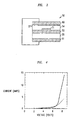
- Figure 1 illustrates the miniband structure of a conventional
optical gain medium 10. Theoptical gain medium 10 includesactive layers 12, 12' andinjector layer 14, which is interposed between theactive layers 12, 12'. The active andinjector layers lower minibands active layers 12, 12', andtransport miniband 20, in theinjector layer 14. The miniband structures are produced by semiconductor superlattice structures in the active andinjector layers - The structure of the upper and
lower minibands active layers 12, 12' fix the wavelength of the light emitted bygain medium 10. In particular, in quantum cascade (QC) lasers, charge carrier transitions from the upper tolower minibands miniband gap 22 separating the upper andlower minibands -
Transport miniband 20 ofinjector layer 14 transports de-excited charge carriers fromlower miniband 18 ofactive layer 12 toupper miniband 16 of adjacent active layer 12'. Thetransport miniband 20 replenishes inverted populations of charge carrier in theupper miniband 16 of the active layer 12'. Thus, theupper miniband 16 is the target upper miniband of the associatedtransport miniband 20. Keeping the inverted population of charge carriers replenished enables further optical emissions from the active layer 12'. - Various embodiments of optical gain medium have injector and active layers in which associated transport and target upper minibands have mismatched lower edges during pumping. The mismatches enable relaxation processes to reduce densities in the active layers of charge carriers that have energies of the associated transport minibands. Reducing densities of such charge carriers in the active layers reduces backward transport of charge carriers through the injector layers. Reducing backward transport increases obtainable inverted populations of charge carriers over those obtainable in optical gain media that are similar except that such mismatches between associated transport and target upper minibands do not exist.
- In one aspect, the invention features an optical gain medium having first and second active layers and an injector layer interposed between the first and second active layers. The active layers have upper minibands and lower minibands. The injector layer has a miniband that transports charge carriers from the lower miniband of the first active layer to an excited state in the upper miniband of the second active layer in response to application of a voltage across the optical gain medium.
- In another aspect, the invention features a process for operating an optical gain medium with a plurality of active layers. The process includes transporting charge carriers from a lower miniband of one of the active layers to an upper miniband of an adjacent one of the active layers and relaxing the transported charge carriers to lower energy states in the same upper miniband.
- In another aspect, the invention features an apparatus that includes an optical gain medium and electrical contacts adjacent opposite sides of the medium. The optical gain medium has a series of stages. Each stage includes an injector layer and an adjacent active layer. The active layers have upper and lower minibands that are separated by a miniband gap Emg. The lower minibands have a width Δlm. The electrical contacts are able to apply a voltage Vps across each one of the stages. Emg is smaller than qVps - Δlm with q being a charge of carriers in the minibands.
-
- Figure 1 shows the miniband structure of a conventional optical gain medium when electrically pumped to generate stimulated optical emission;
- Figure 2 shows the miniband structure of an improved optical gain medium when electrically pumped to generate stimulated optical emission;
- Figure 3 shows an embodiment of a quantum cascade (QC) laser that is based on a gain medium of the type shown in Figure 2;
- Figure 4 shows contrasting electrical characteristics of QC lasers that do and that do not inject charge carriers into excited states of target upper minibands of active layers;
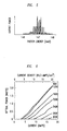
- Figure 5 shows a optical power spectrum of a QC laser of a type shown in Figure 3 when the QC laser is pumped with a 2.5 amp current and operated at about 10 °Kelvin (°K);
- Figure 6 shows optical power-current characteristics of the same QC laser for various operating temperatures;
- Figure 7 is a flow chart for a process of operating the QC laser of Figure 3; and
- Figure 8 is a flow chart for a process for operating a QC laser having the optical gain medium of Figure 2.
-
- Injector layers fix the maximal output optical powers of QC lasers, because the injector layers replenish inverted populations of active regions. Thus, the total transport rate by transport minibands of the injector layers defines the available output optical power of such lasers.
- Referring to Figure 1, in
conventional gain medium 10,transport miniband 20, targetupper miniband 16, and sourcelower miniband 18 have alignedlower miniband edges lower miniband edges transport miniband 20 to perform both forward and backward transport of charge carriers. The backward transport causes charge carriers to move out of the targetupper miniband 16 of active layer 12'. The backward transport reduces the density of charge carriers available to form the inverted population of the targetupper miniband 16. For this reason, the miniband alignment ofgain medium 10 enables lower output optical powers than would otherwise be available in the absence of backward transport of charge carriers. - The amount of backward transport of charge carriers has a direct relation to the density in target active layer 12' of charge carriers with energies of
transport miniband 20. Reducing the density of charge carriers with such energies in the target active layer 12' would reduce backward transport byinjector layer 14. Unfortunately, the alignment oflower edges 24 and 24' fixes the density of charge carriers at energies of thetransport miniband 20 to be equal to the density of charge carriers in the inverted population of the targetupper miniband 16, which is a high density in ideal operating situations. Thus, the miniband alignment in theconventional gain medium 10 favors significant backward transport of charge carriers in ideal operating situations, i.e., high density inverted populations. For this reason, the miniband alignment in theconventional gain medium 10 produces a non-optimal operating situation where significant backward transport lowers the maximum output optical power. - Various embodiments of QC lasers have optical gain medium in which the lower edge of a transport miniband is higher than the lower edge of the associated target upper miniband. This mismatch of lower edges enables relaxation processes to lower densities of charge carriers in the associated target upper miniband at energies of the transport miniband. The lower densities reduce backward transport so that inverted populations of charge carriers can be maintained at higher levels than in gain medium where miniband alignments do not defavorize backward transport of the charge carriers.
- Figure 2 shows several layers of one embodiment of an
optical gain medium 30. Thegain medium 30 includes a sequence ofstages 28, 28' of which two are shown. Eachstage 28, 28' includes aninjector layer 34, 34' and an associated sourceactive layer 32, 32'. Theinjector layer 34 transports charge carriers to the active layer 32' of the next stage in response to electrical pumping. - The
active layers 32, 32' andinjector layers 34, 34' have superlattice structures that produce different miniband structures therein. Theactive layers 32, 32' haveupper minibands 36 andlower minibands 38. By making electronic transitions from theupper minibands 36 to lowerminibands 38 of the sameactive layer 32, 32', charge carriers generate light for stimulated emission or lasing. During stimulated emission. the emitted light has a wavelength that corresponds to the energy Emg of theminiband gap 42. - The injector layers 34 have
transport minibands 40, 40' that transport de-excited charge carriers, i.e., electrons or holes, from a sourcelower miniband 38 to a targetupper miniband 36. The forward transport of charge carriers goes from onestage 28 to the next stage 28'. - Figure 2 shows the miniband structure of gain medium 30 during optimal electrical pumping for stimulated emission. During pumping, the lower edge of
transport miniband 40 is positioned to enable forward transport of charge carriers from a sourcelower miniband 38 ofactive layer 32 to targetupper miniband 36 of adjacent active layer 32'. Pumping facilitates forward transport out of theactive layer 32 by aligning thelower edges transport miniband 40 and sourcelower miniband 38 of thesame stage 28. Herein, such an alignment of a transport miniband and an associated source lower miniband is referred to as a flat-band condition. For the same pumping conditions, backwards transport from the targetupper miniband 36 to the sourcelower miniband 38 is also defavorised, because thelower edge 44 of thetransport miniband 40 is positioned above thelower edge 48 of the targetupper miniband 36. - The mismatch between
lower edges upper minibands upper miniband 36. De-exciting the transported charge carriers lowers the density in the targetupper miniband 36 of charge carrier with energies of thetransport miniband 40. In turn, this de-excitation reduces the probability that the transported charge carriers will propagate backward to source lower miniband 36'. Reducing such backward propagation increases the inverted population in active layer 32' over the population that would exist in a gain medium that was similar except that lower edges of target upper miniband and associated transport miniband matched. - The lower edges 44, 48 of
transport miniband 40 and associated targetupper miniband 36 have a mismatch that is, at least, one to several times the average thermal energy for charge carriers in targetupper miniband 36 at the operating temperature. Preferably, thelower edge 44 is 5 or more times the average thermal energy above thelower edge 48 and more preferably 10 or more times the average thermal energy above thelower edge 48. Since these miniband mismatches are, in each case, greater than the relevant average thermal energy, de-excited charge carriers in theupper miniband 36 are rarely thermally re-excited up to energies oftransport miniband 40. For this reason, intra-band electronic relaxation effectively removes the transported charge carriers from the states of the targetupper miniband 36 with strong probabilities of causing backward propagation via thetransport miniband 40. - Since efficient forward transport requires overlap between transport and target
upper minibands upper minibands upper miniband 36 has a minimum width, Δum. The width, Δum, should, at least, be larger than the average thermal energy of charge carriers in theupper miniband 36, e.g., at 300°K, is preferably 3-5 or more times this average thermal energy and more preferably is 10 or more times this average thermal energy. For such a width, a miniband mismatch can reduce backward transport of charge carriers without interfering with forward transport of the charge carriers. - Figure 3 is a cross sectional view through a Fabry-Perot cavity of a quantum cascade (QC)
laser 50 with thegain medium 30 of Figure 2. The Fabry-Perot cavity is anoptical waveguide 51 that is constructed from anoptical core layer 52 and optical cladding layers 54, 55. The exemplaryoptical waveguide 51 is formed by a ridge whose width, w, is about 38 µm, and whose length of about 2.25 mm long. Other embodiments use optical waveguides that are completely surrounded by optical cladding (not shown). The optical cladding layers 54, 55 have a lower refractive index than thewaveguide core layer 52 so that light is strongly index-confined tooptical waveguide 51. The optical core and cladding layers 52, 54, 55 are made by well-known wet etching. - The core layer 56 is
optical gain medium 30, shown in Figure 2. The gain medium is electrically pumped by a current passing betweenmetallic contacts QC laser 50 at a low temperature to improve performance. To maintain the low temperature, theQC laser 50 is indium-soldered onto a copper holder, which is then mounted in a He-flow cryostat (both not shown). - Referring to Figures 2 and 3, the miniband structure of
gain medium 30 andoptical core layer 52 results from semiconductor superlattice structures in the active andinjector layers optical core layer 52 includes a sequence of stages, i.e., paired active and injector layers, e.g., layers 32, 34 and layers 32', 34'. Theactive layers 32, 32' are intrinsic semiconductor superlattice structures. The injector layers 34, 34' are doped semiconductor superlattice structures that screen external electric fields and produce a selected voltage drop per stage when the gain medium is electrically pumped. The per stage voltage drop, i.e., over a pair of active and injector layers, is (Δlm + Emg + δ)/q. Here, Δlm, Emg, δ, and q are the width of the active layer'slower miniband 38, the active layer'sminiband gap 42, the mismatch betweenlower edges transport miniband 40 and the targetupper miniband 36, and the charge of the current carriers, respectively. This per stage voltage drop produces a miniband alignment that is the same for different stages and large current transport throughinjector layers gain medium 30 is electrically pumped. Thetransport miniband 40 provides transport so that the charge carriers, e.g., electrons or holes, accumulate at the lower edge ofupper miniband 36 after relaxation-induced de-excitation. - Some such lasers generate peak powers of about 2.2 watts per facet at wavelengths of about 8.4 µm and temperatures of about 80°K.
- Performance can be further improved by chirping superlattice active regions or intrinsic superlattices where overlaps between states of laser transition are high so that phonon bottleneck effects are low.
- An exemplary embodiment of
QC laser 50 uses Gallium (Ga) Indium (In) Arsenide (As)/Aluminum (Al) Indium Arsenide -type superlattice structures foractive layers 32, 32' andinjector layers 34, 34'. The superlattices are formed by alternating layers of Ga 0.47 In 0.53 As and layers of Al0.48 In0.52 As. In theactive layers 32, 32', the alternating layers of the superlattice have the following sequence of thicknesses: 2 /3.7/1 /4.1/ 1/ 4.6/ 1/ 4.6/ 1/ 4.6/ 1/ 4.6/ 1/ 4.5/ 1/ 4.3. In the injector layers 34, 34', the alternating layers of the superlattice have the following sequence of thicknesses: 4.0/ 9/ 3.9 / 9 / 3.9/ 1.1/ 3.7/ 1.5/ 3.3/ 1.9/ 2.9/ 2.1/ 2.7/ 2.6/ 2.2/ 3.0/ 1.8/ 3.3. In each sequence, numbers provide layer thicknesses in nanometers, and AlInAs layers and GalnAs layers are bolded and unbolded, respectively. In theactive layers 32, 32', the superlattices are undoped. In the superlattices of the injector layers 34, 34', some GaInAs and AlInAs layers are n-type doped to a dopant density of about 1 x 10¹⁸ per centimeter (cm) cubed. Underlining indicates the n-type-doped superlattice layers in the above sequence. - In the exemplary embodiment of
QCL laser 50,optical core layer 52 includes twenty-fivestages 28, 28' of paired active andinjector layers active stages 28, 38' are sandwiched between the pair of outer GaInAs layers. The outer GaInAs layers having n-type dopant densities of about 5x1016 cm-3. The outer GaInAs layer closest to the InP substrate is about 400 nm thick, and the outer GaInAs layer farthest from the InP substrate is about 220 nm thick. The various layers of the optical core layer are grown over the InP substrate by molecular beam epitaxy processes known to those of skill in the art. - The two optical cladding layers 54, 55 have lower refractive indexes than the active
optical core layer 52. Thelower cladding layer 55 is the InP substrate itself. Theupper cladding layer 55 includes two Al0.48 In0.52 As layers. Each of these AlInAs layers is about 1.2 µm thick each. The two AlInAs layers of the upper cladding layer have n-dopant densities of about 1x1017 cm-3 and about 2x1017 cm-3, respectfully. - Some embodiments of the QC laser also include a
top layer 57 of Ga0.47 In0.53 As. Thistop layer 57 is about 500 nm thick and has an n-type dopant density of about 7x1018 cm-3. Thetop layer 57 provides plasmon-enhanced optical confinement for light that is propagating in the optical waveguide. - The layer sequence of the exemplary embodiment of
QC laser 50 produces the flat-band condition between pairs of source lower minibands 38 andtransport minibands 40 for applied per stage voltages of about 0.330 V. The 0.330 applied per stage voltage is about 35 milli-volts above the onset voltage for strong current injection, i.e., the current threshold for lasing. For the 0.330 applied per stage voltage, thetransport miniband 40 also injects transported charge carriers into high-energy states of targetupper miniband 36. The transported charge carriers are injected into states that are, at least, 3-5 average thermal energies abovelower edge 48 of the targetupper miniband 36 for this pumping current. - Figure 4 compares electrical performance of the exemplary embodiment of QC laser 50 (solid line) with a second QC laser based on a GaInAs/AlInAs superlattice structure. The exemplary and second QC lasers have identical active layers and different injector layers. The injector layers of the second QC laser do not produce a mismatch between transport minibands and target upper minibands of active layers when pumped. While both the exemplary and second QC lasers have onset voltages for lasing of about 7 volts, the two QC lasers behave differently when pumped with currents that are higher than the onset voltage. Above the onset voltage, the exemplary embodiment of
QC laser 50 has a significantly lower resistance than the second QC laser, i.e., a higher current for the same pumping voltage. The lower resistance for above-onset pumping voltages results, in part, from the mismatch between transport and targetupper minibands QC laser 50. - Figure 5 shows the power spectrum of the exemplary embodiment of
QC laser 50 of Figure 3 when pumped with a current of about 2.5 amps at a temperature of about 10°K. The power spectrum has a center wavelength of about 8.4 nm, which corresponds to aminigap 42 of about 151 meV. - Figure 6 shows the optical power-current characteristics of the exemplary embodiment of
QC laser 50 of Figure 3 for operating temperatures in the range of about 80°K to about 300 °K. At 80°K, the output optical power increases approximately linearly with temperature over a range of currents that is several times the size of the lasing threshold current. The exemplary embodiment ofQC laser 50 has output optical powers of 1 watt (W) or more at temperatures below about 200°K, and an output optical power of at least 0.15 watts at temperatures below about 300°K. The output optical power does not saturate for pumping currents of at least 17 amps, i.e., current densities of at least 20 amps/cm2. This performance results from satisfying the flat-miniband and miniband mismatch conditions over the range of above-threshold pumping currents. - Figure 7 illustrates a
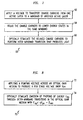
process 60 for operatingoptical gain medium 30 of Figure 2. Theprocess 60 includes applying a pump voltage across the optical gain medium to cause transport minibands to transport charge carriers from alower miniband 38 of oneactive layer 32 to a targetupper miniband 36 of an adjacent active layer 32' (step 62). The applied pump voltage is larger than an onset voltage needed to stimulate optical emissions in theoptical gain medium 30. Theprocess 60 includes relaxing the transported charge carriers to lower energy states in the same targetupper minibands 36 that received the transported charge carriers (step 64). Theprocess 60 includes optically stimulating the relaxed charge carriers to perform inter-miniband transitions that produce light (step 66). The intra-miniband transitions are tolower minibands 38 in the same active layers 32' in which the charge carriers relaxed. - Figure 8 illustrates a process 70 for operating a QC laser having the
optical gain medium 30 of Figure 2, e.g.,QC laser 50 of Figure 3. Theprocess 60 includes applying a pumping voltage, Vp, across theoptical gain medium 30 to transport carriers of charge, q, from oneactive layer 32 to an adjacent active layer 32' (step 72). The applied pumping voltage, Vp, produces a per stage voltage drop, Vps, that satisfies qVps > Δlm + Emg. The process 70 includes optically stimulating carriers in the active layer 32' to make inter-miniband transitions with emission of photons with an average energy, Ecp, that satisfies Eep < qVps - Δlm, i.e., Eep = Emg (step 72). The intra-miniband transitions are tolower minibands 38 in the same active layer 32' to which the charge carriers were transported. Here, qVps - Δlm - Eep is more than the line width, i.e., in energy units, for the light produced by stimulated emission in thegain medium 30. Preferably, Eep is smaller than qVps - Δlm by 3-5 or more times the average thermal energy of the carriers in theupper miniband 36 of the active layers 32'. - Other embodiments of the invention will be apparent to those of skill in the are in light of the specification, drawings, and claims of this application.
Claims (10)
- An apparatus, comprising:an optical gain medium having first and second active layers and an injector layer interposed between the first and second active layers, the active layers having upper minibands and lower minibands; andwherein the injector layer has a miniband that transports charge carriers from the lower miniband of the first active layer to an excited state in the upper miniband of the second active layer in response to application of a voltage across the optical gain medium.
- The apparatus of claim 1, wherein the active and injector layers include semiconductor superlattice structures.
- The apparatus of claim 2, wherein the semiconductor superlattice structures include gallium and arsenic.
- The apparatus of claim 2, wherein the upper miniband of the second active layer has a lower energy state to which charge carriers are able to relax from the excited state.
- The apparatus of claim 4, wherein a lower edge of the miniband of the injector layer has a higher energy than a lower edge of the upper miniband of the second active layer when the voltage is applied.
- The apparatus of claim 5, wherein the apparatus is a quantum cascade laser and a mismatch between the lower edges of the miniband of the injector layer and the upper miniband of the second active layer is larger than an energy associated with the line width of laser light from the quantum cascade laser.
- The apparatus of claim 6, wherein transitions of charge carriers between minibands of the same active layer produce photons during lasing.
- The apparatus of claim 1, wherein the upper minibands have a width Δum that is at least three times the average thermal energy of charge carriers therein at 300°K.
- A process for operating an optical gain medium with a plurality of active layers, comprising:transporting charge carriers from lower minibands of the active layers to upper minibands of adjacent ones of the active layers; andrelaxing the transported charge carriers to lower energy states in the same upper minibands that received the transported carriers.
- The process of claim 9, further comprising:causing a laser cavity to emit light produced by optically stimulating transitions of a portion of the relaxed charge carriers from the upper minibands to lower minibands in the same active layers.
Applications Claiming Priority (4)
| Application Number | Priority Date | Filing Date | Title |
|---|---|---|---|
| 1998-12-15 | |||
| US27317901P | 2001-03-02 | 2001-03-02 | |
| US273179P | 2001-03-02 | ||
| US10/081,313 US6690699B2 (en) | 2001-03-02 | 2002-02-21 | Quantum cascade laser with relaxation-stabilized injection |
Publications (1)
| Publication Number | Publication Date |
|---|---|
| EP1237242A1 true EP1237242A1 (en) | 2002-09-04 |
Family
ID=26765460
Family Applications (1)
| Application Number | Title | Priority Date | Filing Date |
|---|---|---|---|
| EP02251369A Withdrawn EP1237242A1 (en) | 2001-03-02 | 2002-02-27 | Quantum cascade laser with relaxation-stabilized injection |
Country Status (2)
| Country | Link |
|---|---|
| US (1) | US6690699B2 (en) |
| EP (1) | EP1237242A1 (en) |
Families Citing this family (47)
| Publication number | Priority date | Publication date | Assignee | Title |
|---|---|---|---|---|
| US20060231857A1 (en) * | 2003-06-26 | 2006-10-19 | Rj Mears, Llc | Method for making a semiconductor device including a memory cell with a negative differential resistance (ndr) device |
| US20060243964A1 (en) * | 2003-06-26 | 2006-11-02 | Rj Mears, Llc | Method for making a semiconductor device having a semiconductor-on-insulator configuration and a superlattice |
| US7659539B2 (en) | 2003-06-26 | 2010-02-09 | Mears Technologies, Inc. | Semiconductor device including a floating gate memory cell with a superlattice channel |
| US20060289049A1 (en) * | 2003-06-26 | 2006-12-28 | Rj Mears, Llc | Semiconductor Device Having a Semiconductor-on-Insulator (SOI) Configuration and Including a Superlattice on a Thin Semiconductor Layer |
| US20060267130A1 (en) * | 2003-06-26 | 2006-11-30 | Rj Mears, Llc | Semiconductor Device Including Shallow Trench Isolation (STI) Regions with a Superlattice Therebetween |
| US20050279991A1 (en) * | 2003-06-26 | 2005-12-22 | Rj Mears, Llc | Semiconductor device including a superlattice having at least one group of substantially undoped layers |
| US20070063185A1 (en) * | 2003-06-26 | 2007-03-22 | Rj Mears, Llc | Semiconductor device including a front side strained superlattice layer and a back side stress layer |
| US20070063186A1 (en) * | 2003-06-26 | 2007-03-22 | Rj Mears, Llc | Method for making a semiconductor device including a front side strained superlattice layer and a back side stress layer |
| US7586165B2 (en) * | 2003-06-26 | 2009-09-08 | Mears Technologies, Inc. | Microelectromechanical systems (MEMS) device including a superlattice |
| US20060273299A1 (en) * | 2003-06-26 | 2006-12-07 | Rj Mears, Llc | Method for making a semiconductor device including a dopant blocking superlattice |
| US7446002B2 (en) * | 2003-06-26 | 2008-11-04 | Mears Technologies, Inc. | Method for making a semiconductor device comprising a superlattice dielectric interface layer |
| US20050282330A1 (en) * | 2003-06-26 | 2005-12-22 | Rj Mears, Llc | Method for making a semiconductor device including a superlattice having at least one group of substantially undoped layers |
| US20060011905A1 (en) * | 2003-06-26 | 2006-01-19 | Rj Mears, Llc | Semiconductor device comprising a superlattice dielectric interface layer |
| US7531850B2 (en) * | 2003-06-26 | 2009-05-12 | Mears Technologies, Inc. | Semiconductor device including a memory cell with a negative differential resistance (NDR) device |
| US20070015344A1 (en) * | 2003-06-26 | 2007-01-18 | Rj Mears, Llc | Method for Making a Semiconductor Device Including a Strained Superlattice Between at Least One Pair of Spaced Apart Stress Regions |
| US20060220118A1 (en) * | 2003-06-26 | 2006-10-05 | Rj Mears, Llc | Semiconductor device including a dopant blocking superlattice |
| US7612366B2 (en) * | 2003-06-26 | 2009-11-03 | Mears Technologies, Inc. | Semiconductor device including a strained superlattice layer above a stress layer |
| US7535041B2 (en) * | 2003-06-26 | 2009-05-19 | Mears Technologies, Inc. | Method for making a semiconductor device including regions of band-engineered semiconductor superlattice to reduce device-on resistance |
| US7531828B2 (en) * | 2003-06-26 | 2009-05-12 | Mears Technologies, Inc. | Semiconductor device including a strained superlattice between at least one pair of spaced apart stress regions |
| US7531829B2 (en) * | 2003-06-26 | 2009-05-12 | Mears Technologies, Inc. | Semiconductor device including regions of band-engineered semiconductor superlattice to reduce device-on resistance |
| US7514328B2 (en) * | 2003-06-26 | 2009-04-07 | Mears Technologies, Inc. | Method for making a semiconductor device including shallow trench isolation (STI) regions with a superlattice therebetween |
| US7202494B2 (en) * | 2003-06-26 | 2007-04-10 | Rj Mears, Llc | FINFET including a superlattice |
| US7491587B2 (en) * | 2003-06-26 | 2009-02-17 | Mears Technologies, Inc. | Method for making a semiconductor device having a semiconductor-on-insulator (SOI) configuration and including a superlattice on a thin semiconductor layer |
| US20070020860A1 (en) * | 2003-06-26 | 2007-01-25 | Rj Mears, Llc | Method for Making Semiconductor Device Including a Strained Superlattice and Overlying Stress Layer and Related Methods |
| US20060292765A1 (en) * | 2003-06-26 | 2006-12-28 | Rj Mears, Llc | Method for Making a FINFET Including a Superlattice |
| US7598515B2 (en) * | 2003-06-26 | 2009-10-06 | Mears Technologies, Inc. | Semiconductor device including a strained superlattice and overlying stress layer and related methods |
| US7586116B2 (en) * | 2003-06-26 | 2009-09-08 | Mears Technologies, Inc. | Semiconductor device having a semiconductor-on-insulator configuration and a superlattice |
| US20070010040A1 (en) * | 2003-06-26 | 2007-01-11 | Rj Mears, Llc | Method for Making a Semiconductor Device Including a Strained Superlattice Layer Above a Stress Layer |
| US20070020833A1 (en) * | 2003-06-26 | 2007-01-25 | Rj Mears, Llc | Method for Making a Semiconductor Device Including a Channel with a Non-Semiconductor Layer Monolayer |
| US7274719B2 (en) * | 2005-03-09 | 2007-09-25 | Agilent Technologies, Inc. | Buried heterostructure quantum cascade laser |
| US20070030870A1 (en) * | 2005-07-27 | 2007-02-08 | Bour David P | Method and structure for ridge waveguide quantum cascade laser with p-type overgrowth |
| TW200746237A (en) * | 2005-12-22 | 2007-12-16 | Mears R J Llc | Method for making an electronic device including a poled superlattice having a net electrical dipole moment |
| US7517702B2 (en) * | 2005-12-22 | 2009-04-14 | Mears Technologies, Inc. | Method for making an electronic device including a poled superlattice having a net electrical dipole moment |
| US7718996B2 (en) * | 2006-02-21 | 2010-05-18 | Mears Technologies, Inc. | Semiconductor device comprising a lattice matching layer |
| US7781827B2 (en) | 2007-01-24 | 2010-08-24 | Mears Technologies, Inc. | Semiconductor device with a vertical MOSFET including a superlattice and related methods |
| US7928425B2 (en) * | 2007-01-25 | 2011-04-19 | Mears Technologies, Inc. | Semiconductor device including a metal-to-semiconductor superlattice interface layer and related methods |
| US7880161B2 (en) | 2007-02-16 | 2011-02-01 | Mears Technologies, Inc. | Multiple-wavelength opto-electronic device including a superlattice |
| US7863066B2 (en) * | 2007-02-16 | 2011-01-04 | Mears Technologies, Inc. | Method for making a multiple-wavelength opto-electronic device including a superlattice |
| US7812339B2 (en) * | 2007-04-23 | 2010-10-12 | Mears Technologies, Inc. | Method for making a semiconductor device including shallow trench isolation (STI) regions with maskless superlattice deposition following STI formation and related structures |
| US9450053B2 (en) * | 2012-07-26 | 2016-09-20 | Massachusetts Institute Of Technology | Photonic integrated circuits based on quantum cascade structures |
| EP3072158A1 (en) | 2013-11-22 | 2016-09-28 | Atomera Incorporated | Vertical semiconductor devices including superlattice punch through stop layer and related methods |
| US9406753B2 (en) | 2013-11-22 | 2016-08-02 | Atomera Incorporated | Semiconductor devices including superlattice depletion layer stack and related methods |
| WO2015191561A1 (en) | 2014-06-09 | 2015-12-17 | Mears Technologies, Inc. | Semiconductor devices with enhanced deterministic doping and related methods |
| US9722046B2 (en) | 2014-11-25 | 2017-08-01 | Atomera Incorporated | Semiconductor device including a superlattice and replacement metal gate structure and related methods |
| US9941359B2 (en) | 2015-05-15 | 2018-04-10 | Atomera Incorporated | Semiconductor devices with superlattice and punch-through stop (PTS) layers at different depths and related methods |
| US9721790B2 (en) | 2015-06-02 | 2017-08-01 | Atomera Incorporated | Method for making enhanced semiconductor structures in single wafer processing chamber with desired uniformity control |
| US9558939B1 (en) | 2016-01-15 | 2017-01-31 | Atomera Incorporated | Methods for making a semiconductor device including atomic layer structures using N2O as an oxygen source |
Family Cites Families (10)
| Publication number | Priority date | Publication date | Assignee | Title |
|---|---|---|---|---|
| US5457709A (en) * | 1994-04-04 | 1995-10-10 | At&T Ipm Corp. | Unipolar semiconductor laser |
| US5727010A (en) * | 1996-03-20 | 1998-03-10 | Lucent Technologies Inc. | Article comprising an improved quantum cascade laser |
| US5978397A (en) * | 1997-03-27 | 1999-11-02 | Lucent Technologies Inc. | Article comprising an electric field-tunable semiconductor laser |
| US5901168A (en) * | 1997-05-07 | 1999-05-04 | Lucent Technologies Inc. | Article comprising an improved QC laser |
| US5963571A (en) * | 1997-06-30 | 1999-10-05 | Nec Research Institute, Inc. | Quantum-dot cascade laser |
| US6154475A (en) * | 1997-12-04 | 2000-11-28 | The United States Of America As Represented By The Secretary Of The Air Force | Silicon-based strain-symmetrized GE-SI quantum lasers |
| US6091753A (en) * | 1998-05-01 | 2000-07-18 | Lucent Technologies Inc. | Article comprising an improved superlattice quantum cascade laser |
| US6137817A (en) * | 1998-06-12 | 2000-10-24 | Lucent Technologies Inc. | Quantum cascade laser |
| US6501783B1 (en) * | 2000-02-24 | 2002-12-31 | Lucent Technologies Inc. | Distributed feedback surface plasmon laser |
| US6400744B1 (en) * | 2000-02-25 | 2002-06-04 | Lucent Technologies, Inc. | Apparatus comprising a quantum cascade laser having improved distributed feedback for single-mode operation |
-
2002
- 2002-02-21 US US10/081,313 patent/US6690699B2/en not_active Expired - Lifetime
- 2002-02-27 EP EP02251369A patent/EP1237242A1/en not_active Withdrawn
Non-Patent Citations (2)
| Title |
|---|
| SCAMARCIO G ET AL: "High peak power (2.2 W) superlattice quantum cascade laser", ELECTRONICS LETTERS, IEE STEVENAGE, GB, vol. 37, no. 5, 1 March 2001 (2001-03-01), pages 295 - 296, XP006016340, ISSN: 0013-5194 * |
| TROCCOLI M ET AL: "Electronic distribution in superlattice quantum cascade lasers", APPLIED PHYSICS LETTERS, 21 AUG. 2000, AIP, USA, vol. 77, no. 8, pages 1088 - 1090, XP002200818, ISSN: 0003-6951 * |
Also Published As
| Publication number | Publication date |
|---|---|
| US20020136252A1 (en) | 2002-09-26 |
| US6690699B2 (en) | 2004-02-10 |
Similar Documents
| Publication | Publication Date | Title |
|---|---|---|
| US6690699B2 (en) | Quantum cascade laser with relaxation-stabilized injection | |
| Vurgaftman et al. | Mid-IR type-II interband cascade lasers | |
| Heinrichsdorff et al. | High-power quantum-dot lasers at 1100 nm | |
| Shterengas et al. | Cascade pumping of 1.9–3.3 μm type-i quantum well GaSb-based diode lasers | |
| Vurgaftman et al. | High-power/low-threshold type-II interband cascade mid-IR laser-design and modeling | |
| US7756179B2 (en) | Semiconductor laser apparatus | |
| US8374208B2 (en) | Quantum cascade laser | |
| Köhler et al. | Terahertz quantum-cascade lasers based on an interlaced photon-phonon cascade | |
| Grundmann et al. | Progress in quantum dot lasers: 1100 nm, 1300 nm, and high power applications | |
| US7609738B2 (en) | Multiple phonon resonance quantum cascade lasers | |
| Faugeras et al. | High-power room temperature emission quantum cascade lasers at/spl lambda/= 9/spl mu/m | |
| US20020191658A1 (en) | Engineering the gain/loss profile of intersubband optical devices having heterogeneous cascades | |
| US7646797B1 (en) | Use of current channeling in multiple node laser systems and methods thereof | |
| Emanuel et al. | High-efficiency AlGaAs-based laser diode at 808 nm with large transverse spot size | |
| US20180261980A1 (en) | Semiconductor laser | |
| Fujimoto et al. | High-power InGaAs/AlGaAs laser diodes with decoupled confinement heterostructure | |
| Lee et al. | Improvement of catastrophic optical damage (COD) level for high-power 0.98-μm GaInAs-GaInP laser | |
| Thornton et al. | Highly efficient, long lived AlGaAs lasers fabricated by silicon impurity induced disordering | |
| Tredicucci et al. | High-performance quantum cascade lasers with electric-field-free undoped superlattice | |
| Vurgaftman et al. | Physics of interband cascade lasers | |
| EP3893341B1 (en) | Quantum cascade laser element | |
| US7428256B2 (en) | Semiconductor laser device | |
| Lammert et al. | High power (> 10 W from 100 µm aperture) high reliability 808nm InAlGaAs broad area laser diodes | |
| JPH06237041A (en) | High-output semiconductor laser | |
| Chow et al. | Semiconductor Laser Diodes |
Legal Events
| Date | Code | Title | Description |
|---|---|---|---|
| PUAI | Public reference made under article 153(3) epc to a published international application that has entered the european phase |
Free format text: ORIGINAL CODE: 0009012 |
|
| AK | Designated contracting states |
Kind code of ref document: A1 Designated state(s): AT BE CH CY DE DK ES FI FR GB GR IE IT LI LU MC NL PT SE TR |
|
| AX | Request for extension of the european patent |
Free format text: AL;LT;LV;MK;RO;SI |
|
| AKX | Designation fees paid |
Designated state(s): DE FR GB |
|
| 17P | Request for examination filed |
Effective date: 20030422 |
|
| 17Q | First examination report despatched |
Effective date: 20041006 |
|
| STAA | Information on the status of an ep patent application or granted ep patent |
Free format text: STATUS: THE APPLICATION IS DEEMED TO BE WITHDRAWN |
|
| 18D | Application deemed to be withdrawn |
Effective date: 20050217 |