BACKGROUND OF THE INVENTION
Field of the Invention
-
The present invention relates to an image display
system, and more particularly to an image display system
suitable for performing a signal processing of a color image
data using a compressed data.
Description of the Related Art
-
Conventionally, at a time when transmitting /-
receiving a color image, for example, it is adopted a system
of setting up a screen on which a plurality of pixels are
arranged, of defining a scanning system of pixels that
constitute the screen, as well as of sequentially
transmitting color image data with respect to each pixel
based on this scanning procedure, for a television
transmitter, and of displaying the received color image data
in a defined scanning order, on a receiver side. For
example, a CRT (Cathode Ray Tube) is configured to perform a
display for each pixel by projecting an electron beam that
is narrowly focused, onto a surface of a fluorescent
material, and then to display a color image over an entire
screen by scanning the electron beam. In this case, in high
vision broadcasting for a purpose of an enhancement of an
image quality, the number of pixels that constitute the
screen has been increased comparing to the conventional
television broadcasting. Further, in a display device that
is used in a computer terminal and the like, at a time when
enhancing a quality of an image, it is adopted a system of
increasing the number of rewritings (frame rates) of the
display screen as well as an increase of the number of
pixels.
-
On one hand, in a liquid crystal display device, a
plasma display device and the like, it is adopted a
structure (configuration) of constituting a pixel that
becomes a unit of a display as a circuit-like, and of
displaying a color image on a screen, by supplying a display
signal to each pixel while selecting each pixel. In this
kind of display device, it is constituted to display a color
image by inputting data with respect to a color image
through a wire from a display control device that creates or
stores a display data, supplying the inputted data to each
pixel using a driver circuit, and then driving each pixel
sequentially. In this case, as a method of enhancing a
quality of an image to be displayed, increasing the number
of pixels within the screen and/ or of increasing the frame
rate are/is adopted.
-
Incidentally, in order to enhance an image quality, if
the number of pixels and the frame rate are increased, and
thus a capacity of the image data increases, so that, as a
method of decreasing the capacity of the image data, it has
been proposed a compression system that utilizes a
characteristic of an image signal. As one example, in a
still - picture, the JPEG (Joint Photographic Expert Group),
and in animation, the MPEG (Motion Photographic Expert
Group) and the like have been widely adopted. These systems
implement a compression processing of a block in which a
plurality of pixels are combined as a unit, and for the JPEG,
the amount of data of the original picture (image) can be
compressed to the degrees of 1/10 to 1/20. As described
above, even if it is a case of implementing a data transfer
with a limited transmission capacity, by compressing the
data, increasing the number of pixels and the frame rate can
enhance the image quality.
-
In general, enhancing an image quality is equivalent
to increasing an amount of information to be sensed visually,
and this is eventually equivalent to increasing an amount of
data to be displayed. As a result, an enhancement of an
image quality can be planned, by simply increasing the
number of pixels that constitute the screen, or increasing
the number of rewritings (the frame rate "f") of the display
screen, as in the conventional technology. However, for an
increase of the amount of data, it is not possible to
increase the number of pixels and the frame rate all
together under a certain processing capability.
-
That is, assuming that a processing time for a sheet
of screen is "pf", a time required for a generation or an
input of a display data is "pi", and a transfer time of the
display data is "pt", then a processing time for the sheet
of screen "pf" is expressed as pf = pi + pt. Herein, if the
processing time "pf" for the sheet of screen is proportional
to the number of pixels, then increasing the number of
pixels for the purpose of an enhancement of the image
quality causes the processing time "pf" to be extended, and
eventually this causes the frame rate "f" to be decreased.
That is, if the processing time "pf" for the sheet of screen
is a constant (the data generation processing capability = k
pixel/sec.), or if the display capability is a constant, the
display capability is in a relationship of the display
capability = the number of pixels x the frame rate, and thus
two parameters such as the number of pixels and the frame
rate are in the inversely proportional relationship. In
other words, for the increase of the amount of data in the
image data, it is not possible to increase two parameters of
the number of pixels and the frame rate simultaneously,
under a certain device capability.
-
For example, a so-called VGA screen is constituted of
640 horizontal pixels and 480 vertical pixels, and a so-called
UXGA screen is constituted of 3200 horizontal pixels
and 2400 vertical pixels, and the ratio of the number of
pixels between two screens is 1:25. Further, in the common
television broadcasting, a screen of 30 frames per second is
transmitted for reproducing and displaying the motion
pictures, and on one hand, for a screen display of a
computer terminal and the like, a high frame rate such as
120 frame per second is set up, for example, and the ratio
between the frame rates in both cases is 1:4.
-
Now, considering the case that the image data by the
VGA screen is transferred in 30 frames/second, and the image
data by the QUXGA screen is transferred in 120 frames/second,
an amount of data for a display is a multiplication of the
frame rate and the number of pixels, and the ratio of the
amount of data in both cases is 1:100. Accordingly, if
there is no restriction in a data transfer path, at a time
when the amount of data increases along with the increase in
the data generation capability, the increased data can be
easily transferred, if the frame rate is made to be higher,
but if the transfer condition of the data transfer path is
30 frames/second, then for transferring the data
corresponding to 120 frames/second, the amount of data
transfer is restricted by the transfer condition, and thus
it can not be dealt with the increase of the amount of data.
-
As described above, if the processing time "pf" or the
display capability for the sheet of screen is a constant, it
is not possible to increase the number of pixels and the
frame rate simultaneously, along with the increase of the
amount of data.
-
Further, a processing time largely depends on a
capability of a device that performs a screen display, and
thus it is possible that the device for generating the data
and the device for receiving the data have the different
capabilities. For example, if a generation capability of a
display data is equivalent to the one of television
broadcasting, when the display device has the ability of the
QUXGA, then an image that can be displayed in practice is
equivalent to the one of the television broadcasting.
Conversely, even if the processing time "pf" is shortened by
increasing the capability of the device that performs the
processing, there is a case that an upper limit value of the
frame rate "f" possessed by the display device becomes a
restriction. As described above, at a time when processing
the image data, if the capabilities of the device for
generating the data and of the device for receiving the data
are not managed, the capabilities of devices can not be
utilized sufficiently as a whole system.
SUMMARY OF THE INVENTION
-
Accordingly, it is an object of the present invention
to provide a control device, an image display system, an
information processing device, a television receiver, a
transmitter and an image distribution system, which are
capable of suppressing an increase in a load of a data
transfer for an increase of an amount of data.
-
The above-mentioned object of the present invention
can be achieved by a control device, which includes a
compressed data generation unit for generating a compressed
data based on a set-up value inputted, and a controller for
outputting a frame rate information to the compressed data
generation unit, and for making compressed data to be
outputted from a memory for use in storing a compressed data
to an image display device in accordance with the frame rate.
-
The above mentioned object of the present invention
can also be achieved by an image display system, which
includes an image display device for displaying an image in
accordance with an image information, a memory for storing a
compressed data, and a controller for making the compressed
data to be outputted from the memory to the image display
device in accordance with a frame rate.
-
The above mentioned object of the present invention
can be achieved by an image display system, which includes
an image display device for displaying an image in
accordance with an image information, a compressed data
generation unit for generating a compressed data based on a
frame rate and an image information, and a controller for
outputting an information of a frame rate to the compressed
data generation unit.
-
The above-mentioned object of the present invention
can be achieved by an image display system, which includes
an image display device for displaying an image in
accordance with an image information, a compressed data
generation unit for generating a compressed data based on a
frame rate and an image information, and a controller for
outputting a frame rate information to the compressed data
generation unit, and for making the compressed data to be
outputted from a memory for use in storing a compressed data
to the image display device in accordance with the frame
rate.
-
The above-mentioned of the present invention can be
achieved by an information processing device, which includes
an image display device for displaying an image in
accordance with an image information, and a control device
for outputting an image information to the image display
device, wherein the control device includes an image
information generation unit for generating an image
information, a compressed data generation unit for
generating a compressed data based on a frame rate and an
image information, and a controller for outputting a frame
rate information to the compressed data generation unit, and
for making the compressed data to be outputted from a memory
for use in storing a compressed data to the image display
device in accordance with the frame rate.
-
The above-mentioned object of the present invention
can be achieved by a television receiver, which includes an
image display device for displaying an image in accordance
with an image information, and a control device for
outputting an image information to the image display device,
wherein the control device includes a receiving unit for
receiving an image information, a compressed data generation
unit for generating a compressed data based on a frame rate
and an image information received by the receiving unit, and
a controller for outputting a frame rate information to the
compressed data generation unit, and for making the
compressed data to be outputted from a memory for use in
storing a compressed data to the image display device in
accordance with the frame rate.
-
The above-mentioned object of the present invention
can be achieved by a transmitter, which includes an image
information generation unit for generating an image
information, a compressed data generation unit for
generating a compressed data in accordance with a
predetermined transmission rate and the image information,
and a transmission unit for transmitting the compressed data.
-
The above-mentioned object of the present invention
can be achieved by an image distribution system, which
includes a first recording unit for recording a distribution
request from a user and an information about an image
display device of which the user possesses, on a recording
medium through a telecommunication line, a second recording
unit for recording a transmission rate of an image
information on the recording medium, a compressing unit for
compressing an image information to be displayed on the
image display device, in accordance with the distribution
request, the information about the image display device and
the transmission rate, a transmission unit for transmitting
the compressed image information, and an accounting unit for
processing the distribution request recorded on the
recording medium or the information of the image display
device, and for performing an accounting in response to a
result of the processing.
-
According to the above-described units, it is
configured to change the compression rate of data along with
the frame rate, so that the increase in the load of the data
transfer can be suppressed for the increase of the amount of
data. More concretely, by increasing the data compression
rate along with the increase of the frame rate, the contrary
conditions of the number of pixels and of the frame rate can
be relaxed. As a result, by transferring the compressed
data in which the compression rate of data has been changed
along with the frame rate to the image display device, it
can be contributed to an enhancement of the image quality.
-
Further objects and advantages of the invention can be
more fully understood from the following detailed
description taken in conjunction with the accompanying
drawings in which:
BRIEF DESCRIPTION OF THE DRAWINGS
-
- Fig. 1A is a block diagram showing a structure of an
image display system according to one embodiment of the
present invention;
- Fig. 1B is a block diagram showing a structure of an
image display system according to another embodiment of the
present invention;
- Fig. 2 is a block diagram showing a structure of a
display device according to the present invention;
- Fig. 3 is a diagram for illustrating the structures of
an address generation control signal and a compressed data
generation control signal;
- Fig. 4 is a diagram for illustrating a relationship
between a diagram structure and a pixel block;
- Fig. 5 is a diagram for illustrating a relationship
between a display device and a display data in a compression
rate set - up;
- Fig. 6 is a diagram for illustrating a transfer method
of a compressed data;
- Fig. 7 is a diagram for illustrating a generation
method of a compressed data;
- Fig. 8 is a block diagram showing an entire structure
of a display device according to the present invention;
- Fig. 9 is diagram enlargedly showing a portion of a
display area in order to illustrate a write situation into a
pixel for each frame in the embodiment shown in Fig. 8;
- Fig. 10 is a circuit diagram showing an embodiment of
a pixel circuit structure for implementing an image area
separation display according to the present invention;
- Fig. 11 is a timing chart showing an example of a
driving voltage waveform to be applied to each wire, in
order to perform the image area separation display according
to the present invention;
- Fig. 12 is a block diagram showing an entire structure
of a display device according to another embodiment of the
present invention;
- Fig. 13 is a circuit diagram showing an example of the
pixel unit 300 shown in Fig. 12;
- Fig. 14 is a circuit diagram showing an example of a
detailed circuit structure of the pixel unit 300 shown in
Fig. 12;
- Fig. 15 is a diagram for illustrating an operation of
the signal comparator shown in Fig. 14;
- Fig. 16 is a diagram for illustrating a control
operation of the display device shown in Fig. 12;
- Fig. 17 is a timing chart for illustrating a control
operation of the display device shown in Fig. 12;
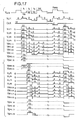
- Fig. 18 is a diagram for illustrating a negotiation
procedure of a device capability;
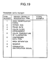
- Fig. 19 is a diagram for illustrating a negotiation of
a device capability;
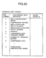
- Fig. 20 is a diagram for illustrating a data structure
of a data transfer;
- Fig. 21 is a block diagram showing a structure at a
time when applying the present invention to a transmitter;
- Fig. 22 is a block diagram showing a structure at a
time when applying the present invention to an image
distribution system;
-
DESCRIPTION OF THE PREFERRED EMBODIMENT(S)
-
In the following, the preferred embodiments of the
present invention will be described with reference to the
accompanying drawings.
-
Fig. 1A is a block diagram showing a structure of an
image display system according one embodiment of the present
invention. In Fig. 1A, the image display system is
constituted of a display control device 200, a data transfer
device 211, and a display device (image display device) 212.
-
The display control device 200 is configured to, as an
element of a video card, input a screen structure of the
display device 212, a data concerning a frame rate (frame
rate information) or a color image data as an image
information, from a keyboard, for example, to compress the
inputted data in a compression rate (data compression rate)
matching with a frame rate, and to transfer the compressed
data to the display device 212 through the data transfer
device 211. At a time when compressing the data, as shown
in Fig. 1B, it may also adopt a structure to input an image
information, for example, a color image data, according to a
generation of the processor (CPU) 210 connected to the
display control device 200, and then to compress the
inputted data in the display control device 200.
-
The display device 200 is, as shown in Fig. 2,
constituted of a management unit 201, a compressed data
generation unit 202, a compressed data memory 203, and an
address generation unit 204. The management unit 201 is
configured to input a data including a screen structure, a
frame rate, and a color image information, to generate a
compressed data generation control signal and an address
generation control signal based on the inputted data, to
output the compressed data generation control signal to the
compressed data generation unit 202, and to output the
address generation control signal to the address generation
unit 204.
-
The compressed data generation signal and the address
generation signal are, as shown in Fig. 3, constituted of
signals including information of a frame rate (100 fps, 50
fps,...), a block size (1000 x 1000, 640 x 480, ...), a number
of analogous colors (two colors, four colors, ...), areas
(animation area, still-picture area, ...), and a clock.
-
The address generation unit 204 is configured to
generate a write address and a read address, as a memory
address associated with each pixel that constitutes the
color image, in response to the address generation control
signal, and to sequentially output the memory addresses for
the write/read to the compressed data memory 203. The
memory address for writing the data is generated using the
information such as a format and a timing of the data input,
a type of the compressed data, a screen structure of the
display device 212 and the like. On one hand, the memory
address for reading the data is generated using the
information such as a type of the compressed data, a screen
structure of the display device 212, a frame rate and the
like. When performing the read or the write of data in
accordance with the memory addresses generated, it is
configured to perform a control with a dihedral memory
structure in order to prevent the operations of the read and
the write of data from interfering each other. Further,
when making the type of compressed data and the like to be
variables, based on the signal characteristics of image, it
enables the generation method of addresses to change in
matching with the type of compressed data.
-
The compressed address generation unit 202 is
configured to compress the color image data, in accordance
with the frame rate as the set - up value (predetermined
value), in response to the compressed data generation
control signal, and to transfer the compressed data together
with a header information to the compressed data memory 203.
-
The compressed data memory 203 is configured to store
the compressed data into a designated memory area in
response to the memory address for the write, as a memory
(storage medium) for storing the compressed data, to read
the compressed data from the designated memory area in
response to the memory address for the read, and to output
the compressed data read as a display data to the data
transfer device 211.
-
That is, the management unit 201, the address
generation unit 204 are configured to have an capability of
a controller so as to output an information concerning the
frame rate to the compressed data generation unit 202, at a
time when the data concerning the color image data is
inputted, as well as to read the compressed data from the
compressed data memory 203, in response to the frame rate,
and then to cause the compressed data read, as a display
data, to be outputted to the display device 212 through the
data transfer device 211.
-
The compressed data generated by the compressed data
generation unit 202 is generated in that a block of which a
plurality of pixels are combined is a unit, as shown in Fig.
4. It is performed with the block unit when the compressed
data generated by the compressed data generation unit 202 is
transferred or stored, as well as it is performed with the
block unit when an elongation-process is performed on the
transferred data. The parameters such as a shape and a size
of this block, a number of pixels to be included in the
block may be set - up with a fixed value, or it may be set-up
as variables based on the characteristics of the image
signal, and a compression rate may be established based on
the set-up parameters. Further, in a sheet of an image, the
parameters may be set-up as variables by separating the
image areas based on the signal characteristics. Moreover,
when generating a compressed data, it may be generated by
implementing a compression process as making an image data
for a pixel (of a pixel unit) inputted from the processor
210 to be a subject thereto, or a compressed data may be
generated based on a plotting command.
-
The data transfer device 211 may be constituted of a
data transmission line in which a lead is used, as well as
of a wireless data transmitting means or an optical data
transmission line. In this case, the image data by the
compressed data is transferred along with a control signal,
and an electric power may be transmitted simultaneously if
necessary. Then, if the image data to be transferred
follows with a predefined data format, a transmission
procedure and the like, the same image data may be
rearranged on the receiving side, i.e., the display device
212 side.
-
The data transfer device 211 is in that an upper limit
of a rate with which a data transfer can be made stably is
defined in many cases, and in general, a transfer rate is
expressed in a unit of bps (bit per second) and the like.
This value is to define a time "pt" required for a certain
data transfer. Under the condition as the time "pt" being
defined, in the present embodiment, as will be described
later, assuming the data to be transferred as a compressed
type, it is arranged that a substantial transfer rate is
enhanced, and the process time "pt" is shortened.
-
On one hand, the display device 212 is constituted by
using a liquid crystal display device of an active matrix
type, for example, and an upper limit "fup" of a physical
frame rate possessed by the display device itself is set-up,
by electrical operation conditions such as an element
structure, a wiring, a driver structure and the like.
However, in the present invention, because the data
compression rate is to be changed in matching with the frame
rate, the compressed data would not be elongated, and by
directly utilizing it as a display data, an operation
condition can be eased by reducing an amount of signal to be
driven by a driver, thereby it is arranged to enhance the
frame rate "fup" of the display device 212 itself. Further,
in a case that an elongation device is integrated into the
display device itself, a compatibility of an interface can
be implemented, because an operation of a driver of the
display device 212, a signal flowing through a wiring, and
the like become the same as the ones of the conventional
driving conditions per pixel unit.
-
As described above, the image display system in the
present embodiment is planning to enhance a device
capability (the upper limit "fup" of the frame rate) of the
display device itself, as the above-mentioned capabilities
(abilities) to be the fundamental structures, to shorten the
process time "pf" (= pi + pt) or to improve a display
capability (= the number of pixels x the frame rate), so as
to enhance an image quality.
-
More concretely, as shown in Fig. 5, the frame rate
"f" depends on the timing "pf" of the display data inputted
into the display device, and it becomes as "f = 1/pf". As a
result, it is arranged to set-up the processing time "pf" in
such a manner that the "f" approaches to the "fup".
-
Herein, if the processing time "pf" could be 1 / 2 as
a result of the compression rate of data being 1/2, then,
from the above-mentioned relational expression, the frame
rate capable of displaying the inputted data can be set-up
in two-holds. However, the upper limit value "fup" defined
by the device capability of the display device itself can
not be exceeded. Accordingly, the processing time "pf" can
be defined as the upper limit value "fup" being the
constraint.
-
Further, by using the display control device 200,
performing a negotiation procedure for exchanging the
capabilities among the devices, a set-up of the compressed
data type, the image area separation based on the image
content, and adjusting the processing time "pf" and the
display frame "f", it is also possible to enhance the image
quality while utilizing the device capabilities.
-
Moreover, in a case that the generation time "pi" of
the compressed data can be made approximately zero ("0"),
with an invent such as the dihedral memory structure, an
influential factor of the processing time "pf" becomes the
data transfer time "pt". In this case, if the transfer rate
of the data transfer device 211 has already defined, then
the influential factor becomes an amount of data per screen
(= processing time "pf" x transfer rate). That is, the
compression rate becomes a large factor to determine the
characteristics of the device as a whole. However, in the
systems such as the JPEG, MPEG in which the compression
rates vary with the patterns, the processing time can not be
established in advance, and thus the device design becomes
difficult. On the contrary, the processing time can be
established in advance by adopting a compression system in
which the compression rate is to be fixed by the parameter
set-up, as in the present invention.
-
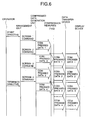
When transferring the compressed data, as shown in Fig.
6, the commands concerning the screen 1 to the screen 4 are
inputted based on the start directive and the terminate
directive of the operator, the compressed data 1 to 4
concerning the screen 1 to 4 are generated based on the
commands inputted, and it makes possible to display the
images that follow the respective commands onto the screen
of the display device 212 by iterating the processes of
transferring the compressed data 1 to 4 to the display
device 212 through the data transfer device 211 after having
stored the compressed data 1 to 4 into the compressed data
memory 203. In this case, although the frame rate of the
display is substantially controlled by the data transfer
time, in order to shorten the transfer time, utilizing the
compressed data may enhance the frame rate.
-
Further, when transferring the compressed data, the
generation time "pi" of the compressed data as seeing from
the data output side could be made approximately zero "0" by
constituting the compressed data memory 203 with the one
having the capacity to store the compressed data for two
screens, for example, two memories, as well as constituting
the switches on both sides of each memory, and arranging
them (the switches) to enable the processes of writing the
data for one screen into one of the memories through one of
the switches, and reading the data for one screen from the
other memory through the other switch, and thereby
alternately switching the memories which perform the reading
of data and the writing of data.
-
Moreover, as other memory arrangement, for a block
constituted of a plurality of pixels as a unit of a
compression, for example, the processes of writing the data
and of reading the data in the block unit could be performed
simultaneously by arranging the memory in a dihedral
structure. In addition, the compressed data memory 203 may
be no longer required by arranging the generation of the
compressed data to be faster than the data transfer rate.
-
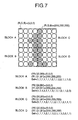
In the following, a concrete generation method of a
compressed data will be described. At a time when
generating the compressed data, it is assumed that the
inputted image is a two-dimensional image of which several
pixels are arranged on a plane, the inputted image is
divided into a block constituted of a plurality of pixels,
and the compression processing procedures for a block unit
is performed. In this case, a size of the block is not
restricted, but it may be configured as 4 (four) in vertical
and 4 (four) in horizontal (total 16 pixels/block), as shown
in Fig. 7, for example. Further, a color signal of each
pixel is not restricted, but here it is assumed to have the
color signal of (Rij, Gij, Bij), (i, j = 0 to 3), and as an
example of the compression procedure, it will be described
for a case that as the kind of colors appeared within the
block to be two kinds, the color signal within the block is
approximated to two kinds.
- (1) Measuring the amplitudes of the color signals (Rij,
Gij, Bij), for all pixels (16 pixels) with the block A.
- (2) Calculating the average value Cave, for the color
signal C with the largest amplitude, within the block A.
The color signal C may be any one of the RGB. Further, it
may be varied for each block.
- (3) Grouping all pixels within the block according to
the large/small comparisons with the average value Cave of
the color signal C. A number of pixels to be grouped into
each group are not restricted.
- (4) Calculating the average for two groups (R0, G0,
B0), (R1, G1, B1). Then, representing the inside of the
block A, by approximating with these two kinds of color
signals.
- (5) Approximating each pixel within the block A with
either one of the two kinds of color signals (R0, G0, B0),
(R1, G1, B1). As a result, a choice of two kinds of color
signals is represented in 1 bit signal.
- (6) Iterating the same processes from the above-mentioned
(1), for the next blocks B to D.
-
-
According to the above-mentioned procedures, it may be
represented by the two kinds of color signals (R0, G0, B0),
(R1, G1, B1) for each block, and by a signal indicating the
choice of two things for each pixel.
-
For example, when writing a black character onto a
white background for each of the blocks A to D, as analogous
color signals within each block, the white background (R, G,
B) = (0, 0, 0), and the black (R, G, B) = (255, 255, 255)
are set-up. Then for selecting each of the analogous color
signals, a pixel of the white background is set-up to 1, and
a pixel constituting the character is set-up to 0,
respectively.
-
Here, in a case that the color signal is 8 bits, 1
(one) block of the inputted images becomes as 16 pixels x 3
colors x 8 bits = 384 bits/block. On one hand, a compressed
data generated by the above-mentioned procedures becomes as
3 colors x 8 bits x two kinds x a signal indicating the
choice of two things for each pixel 1 bit x 16 pixels = 64
bits. Comparing the two, it is apparent that the data is
compressed to 1/6 of the original image data. As described
above, in a step of the data generation, the process load
may be reduced to 1/6. With the same ratio, the shortenings
of the memory capacity and the memory writing time may be
implemented. Further, this method has a feature that the
compression rate is always a constant since the amount of
data of the compressed data to be generated is not affected
by the pattern within the block.
-
In the above-mentioned embodiment, the inside of block
is represented by the two kinds (white and black) of
analogous color signals, but it is not intended to limit the
kind and the number thereof. Further, as he parameters of
the compression processes, the block size, the kind of
analogous colors within the block, the number of bits for
the color signal and the like may be set-up.
-
A profile information becomes important for an area at
where there is motion, and on the contrary, if it is not
sensed as the number of bits of the color signal is reduced,
then the amount of data may be reduced by representing a 8-bits
signal with 6 bits, for example. In this case, it
becomes the total of 52 bits as 36 bits (= two kinds x 3
colors x 6 bits) representing the two kinds of analogous
color signals and the selection signal 16 bits (= 16 pixels
within the block) for each pixel, and the compression rate
becomes 52/384 (= approximately 1/7.4).
-
The above-mentioned procedures implement the grouping
(3) using the average value Cave calculated in the procedure
(2), in order to simplify the processing. That is, each
pixel is classified according to only a single color signal
C. However, it is not limited to this classifying method,
but the grouping may be made by performing a distance
calculation on a color space.
-
The parameters such as the block size, the number of
analogous colors within the block and the like may be
modified arbitrarily in the above-mentioned procedures. The
compression rate may be set-up along with this set-up of the
parameters.
-
In the following, one embodiment of the image display
device according to the present invention will be described
in accordance with Fig. 8. Fig. 8 is a block diagram
showing an entire structure of the image display device 212.
The image display device 212 in the present embodiment is
constituted of a display controller 10, an image conversion
circuit 11, and a display panel 15. The display controller
10 converts the image data (compressed data) from the data
transfer device 211 to a display data. The image conversion
circuit 11 is constituted of a frame memory, which sends the
data with different resolutions to the display panel 15, and
an animation discriminate circuit.
-
On the periphery of the display panel 15, a signal
driver 12 for applying an image data signal to the display
panel 15, a gate driver 13 for applying a scanning signal to
the display panel 15, and a pixel selection driver 14 for
applying a selection signal which selects a display block
are arranged.
-
The display panel 15 is capable of optionally
switching an animation area 15A in which a plurality of
pixels within one block is selected in one scanning period
of time simultaneously and the same content is displayed,
and a still-picture area 15B in which a plurality of pixels
within 1 block are selected by multiple times of scanning
and the different displays are possible for each selection,
with a plurality of pixels among which several pixels are
arranged in a matrix shape as 1 block unit.
-
In the image display device 212 of the present
embodiment, for the plurality of pixels, it implements a
smooth display of an animation by displaying the data with
the low resolution in one scanning period of time
simultaneously, and it also implements a highly minute
display of a still-picture by displaying the data with high
resolution in multiple times.
-
Although a detailed structure of the display panel 15
will be described later, the animation area 15A, in which
input signals from the signal driver 12, the gate driver 13
and the pixel selection driver 14 are selected for a
plurality of pixels within one block in one scanning period
of time simultaneously and the same content is displayed,
and the still-picture area 15B in which the input signals
are selected by the scanning of multiple times, for the
plurality of pixels within 1 block and the different
displays are possible for each selection may be optionally
selected, and the sizes and the display locations may be
changed.
-
It makes also possible to switch the still-picture
area 15B in Fig. 8 to the animation area 15A, and to switch
the current animation area 15A to the still-picture 15B.
-
It may also adopt a system to divide the inside of
block into two sub-blocks, for example, and to display the
same information on each of the sub-blocks, for the still-picture
which may be only with a relatively low minuteness,
in matching with a minuteness of the still-picture to be
displayed.
-
In the present specification, for a case of the color
display, one pixel is constituted of 3 pixels of red, green
and blue, and for a case of the monochrome display, it is
assumed that one pixel is equal to one pixel.
-
Fig. 9 is a diagram enlargedly showing a portion of
the display area for illustrating a write situation into a
pixel for each frame in the present embodiment. In the
present embodiment, 4 pixels of 2 x 2 pixels are defined as
1 block unit.
-
First, in the first frame 100, the high minute still-picture
area writes the image data a(1) 1,1 into the pixel 150,
and similarly, to other high minute still-picture areas, the
image data is written into one pixel within four pixels,
respectively.
-
On one hand, the low minute animation area writes the
same image data a(1) 3,0 into four pixels 160, and similarly,
to other low minute animation areas, the same image data is
written into four pixels, respectively.
-
In the second frame 101, the high minute still-picture
area holds the image data a(1) 1,1 of the pixel 150 written
into the previous frame, and newly writes the image data a(2)
1,2 into the pixel 151 which is different from the previous
frame within the block, and similarly, to other high minute
still-picture areas, the image data is written into one
pixel that is different from the previous frame,
respectively.
-
On one hand, the low minute animation area writes the
same and the new image data a(2) 3,0 into four pixels 161, and
similarly, to other low minute animation areas, the same and
new image data is written into four pixels, respectively.
-
In the third frame 102, the high minute still-picture
area holds the image data of the pixels 150, 151 written
into the first and second frames, and newly writes the image
data a(3) 1,3 into the pixel 152 which is different from the
first and second frames within the block, and similarly, to
other high minute still-picture areas, the image data is
written into one pixel that is different from the first and
second frames, respectively.
-
On one hand, the low minute animation area writes the
same and the new image data a(3) 3,0 into four pixels 162, and
similarly, to other low minute animation areas, the same and
new image data is written into four pixels, respectively.
-
Further, in the fourth frame 103, the high minute
still-picture area holds the image data of the pixels 150,
151, 152 written into the first, second and third frames,
and newly writes the image data a(4) 1,4 into the pixel 153
which is different from the first, second and third frames
within the block, and similarly, to other high minute still-picture
areas, the image data is written into one pixel that
is different from the first, second and third frames,
respectively.
-
On one hand, the low minute animation area writes the
same and the new image data a(4) 3,0 into four pixels 163, and
similarly, to other low minute animation areas, the same and
new image data is written into four pixels, respectively.
-
By iterating the above described processes, the high
minute still-picture display area and the low minute
animation display area can be displayed in arbitrary areas
within the display area.
-
The high minute still-picture area forms a high minute
image with four frames, and the low minute animation area
can display a new data for each frame. Accordingly, the
still-picture having no variation within four frames can be
displayed in a high minute, and the animation with a rapid
motion can be fast-displayed for each frame.
-
In the present specification, a display system for
displaying by varying a resolution of an arbitrary area
within a display area as described above is called as an
image area separation display system.
-
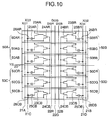
Fig. 10 is a circuit diagram showing an embodiment of
a pixel circuit structure for implementing an image area
separation display according to the present invention.
-
The present embodiment is a pixel circuit structure of
which 2 x 2 pixels are made as 1 block unit, and an entire
display area of the display panel 15 is formed by arranging
a large number of this pixel circuit structures. One block
unit is not restricted to four pixels. However, in
considering a degradation of an opening ratio caused by an
increase of wiring and the like, one block with four pixels
is preferable.
-
The image display device using the image area
separation display system of the present invention is not
restricted to the liquid crystal display, and it is
applicable to the ELD, FED, PDP and the like. Here, the
present invention will be described with the liquid crystal
display that is the most suitable as an example.
-
The liquid crystal display of the present embodiment
is constituted of an illumination device on the background,
and includes a pair of transparent substrates having
polarizing plates and a liquid crystal layer sandwiched
between these pair of transparent substrates, and is
configured to control an orientation state of the liquid
crystal layer by applying an electrical field to the liquid
crystal layer, and to display an image.
-
In the circuit structure of 1 block pixel with four
pixels in Fig. 10, for each elements, providing, after a
number, A to an upper left pixel, B to an upper right pixel,
C to a lower left pixel, and D to a lower right pixel, and
further providing R, G, B for the pixels of Red, Green and
Blue, correspondingly.
-
In the present embodiment, one block is formed by four
pixels of the pixels 50A, 50B, 50C, 50D. The pixel 50A is
constituted of three pixels of the Red 50AR, the Green 50AG,
and the Blue 50AB. The pixel 50B is constituted of three
pixels of the Red 50BR, the Green 50BG, and the Blue 50BB.
The pixel 50C is constituted of three pixels of the Red 50CR,
the Green 50CG, and the Blue 50CB. The pixel 50D is
constituted of three pixels of the Red 50DR, the Green 50DG,
and the Blue 50DB.
-
A scanning wiring 20 that is a common to the four
pixels is formed at a center, and twelve gates of the thin
film transistors 24AR, 24BR, 24CB, 24DB and the like that
are the first switches are connected to the scanning wiring
20.
-
A block selection signal wiring 21A is connected to
the drain electrodes of the thin film transistors 24AR, 24AG,
and 24AB that are the first switches. A block selection
signal wiring 21B is connected to the drain electrodes of
the thin film transistors 24BR, 24BG, and 24BB. A block
selection signal wiring 21C is connected to the drain
electrodes of the thin film transistors 24CR, 24CG, and 24CB.
A block selection signal wiring 21D is connected to the
drain electrodes of the thin film transistors 24DR, 24DG,
and 24DB.
-
The thin film transistors 24AR, 24AG, 24AB that are
the first switches are the switches for selecting the pixel
50A, respectively, and can also be formed as one by a
commonization. Similarly to the pixels 50B, 50C, 50D, the
first switches can also be formed as one by a commonization.
-
Twelve gate electrodes of the thin film transistors
23AR, 23BR, 23CB, 23CB and the like that are the second
switches are connected to the source electrodes of the thin
film transistors that are the first switches.
-
A red color image signal wiring 22R, a green color
image signal wiring 22G, and a blue color image signal
wiring 22B are connected to the drain electrodes of the thin
film transistors that are the second switches, respectively.
-
To the source electrodes of the thin film transistors
that are the second switches, the pixel electrodes are
connected, respectively, and the counter electrodes 26AR,
26BR, 26CB, 26DB and the like are connected thereto, by
sandwiching the liquid crystal layer, so that they form the
pixel units 25AR, 25BR, 25CB, 25DB and the like.
-
The counter electrodes are the electrodes that are
common to all pixels. To the pixel units 25AR, 25BR, 25CB,
25DB and the like, the holding capacitors are formed in
parallel.
-
By adopting the image circuit structure such as
described above, it makes possible the image area separation
display illustrated in Fig. 9.
-
In the present embodiment, in Fig. 10, although the
scanning wiring 20 is connected to the gates of the first
switches and the block selection signal wiring is connected
to the drain electrodes of the first switches, but it may be
arranged as a structure of which the block signal selection
wiring for each pixel is connected to the respective gates,
and the scanning wiring 20 is connected to the drain
electrodes of all four pixels.
-
Fig. 11 is a timing-chart showing an example of a
driving voltage waveform to be applied to each wiring in Fig.
10 in order to perform an image area separation display.
Consider the j-th scanning wiring Y(j). To the scanning
wire Y(j), a gate voltage 30 which turns on the thin film
transistors that are first switches for every frame period
of time 34 is applied. In synchronization with this gate
voltage 30, in the area for performing a high minute display,
the voltages 32A to 32D are applied to the block selection
signal wiring X(i)1 to X(i)4 21A to 21D for each 4 blocks,
respectively, and in synchronization with the gate voltage
30, the image signals 31 corresponding to the red color
D(i)R, the green color D(i)G, and the blue color D(i)B are
applied to the pixels through the second switches.
-
Accordingly, only either one of the pixels 50A, 50B,
50C and 50D is selected. Further, in the pixels not to be
selected, the voltages are held, during four (4) frames.
-
On one hand, in the area for performing a low minute
display, the voltage 33 is applied to 21A to 21D that are
the block selection signal wiring X(i)all for each frame,
respectively, and in synchronization with the gate voltage
30, the image signals 31 corresponding to the red color
D(i)R, the green color D(i)G, and the blue color D(i)B are
applied to the pixels through the second switches.
Accordingly, the same signal is applied to all of the pixels
50A, 50B, 50C, 50D, and thus the same display for four
pixels can be rewritten for each frame.
-
For the j+1-th scanning wiring Y(j+1), similarly to
the j-th wiring, it discriminates whether it is the high
minute display area or the low minute display area, and by
inputting the above-mentioned driving waveform, it makes
possible a display of an image area separation.
-
Consequently, by displaying a still-picture in the
high minute area and an animation in the low minute area,
even in the display mixed of the animation and the still-picture,
the animation can be rewritten in fast-speed, and
the still-picture is displayed in the high minute.
-
In the following, another embodiment of the display
device 212 according to the present invention will be
described with reference to Fig. 12. Fig. 12 is a block
diagram showing an entire structure of the display device
212 according to the present invention. The display device
212 in the present embodiment is constituted of n-levels of
gray approximation arithmetic circuit 310 for converting the
inputted image signal to a n-levels of gray approximate
image signal approximated to a gray level of a binary value
for each block, a signal control circuit 320 for supplying
predetermined signals to the X driver 330, the Y driver 340,
the common voltage generation circuit 350, and the signal
supply circuit 360 in accordance with the n-levels of gray
approximation image signals outputted from the n-levels of
gray approximation arithmetic circuit 310, and a plurality
of pixel units 300 provided at an intersection unit of a X
signal line 331 connected to the X driver 330 and extended
to the Y direction and a Y signal line 341 connected to the
Y driver 340 and extended to the X direction.
-
Fig. 13 is a circuit diagram showing an example of a
structure of the pixel unit 300. To the pixel unit 300, the
X signal Vx is supplied from the X driver 330 through the X
signal line 331. To the pixel unit 300, the Y signal VY is
supplied from the Y driver 340 through the Y signal line 341.
To the pixel unit 300, the liquid crystal driving signal VLCD
is supplied from the signal supply circuit 360 through the
liquid crystal driving signal line 361. In addition, to the
pixel unit 300, the common voltage VCOM is supplied from the
common voltage generation circuit 350 through the common
voltage line 351.
-
The pixel unit 300 is constituted of a XY arithmetic
circuit 310 connected to both the X signal line 331 and the
Y signal line 341, a signal comparator 320 connected to the
XY arithmetic circuit 310, a switch 332 which is controlled
in response to an output of the signal comparator 320, a
pixel electrode 340 of which a connection to the liquid
crystal driving signal line 361 is controlled by the switch
332, and a liquid crystal 352 arranged between the pixel
electrode 340 and the common voltage line 351. As shown in
Fig. 12, the pixel unit 300 is divided into the block 360
that consists of the total of 16 pixel units of 4 columns in
the X direction and 4 rows in the Y direction.
-
Fig. 14 is a circuit diagram showing an example of a
detailed circuit structure of the pixel unit 300. The XY
arithmetic circuit 310 is constituted of a capacitor 111
connected to a terminal to which the Vx is supplied from the
X signal line 331, a capacitor 312 connected to a terminal
to which the VY is supplied from the Y signal line 341, and a
p-type MOS-TFT 313 which operates in response to a clock
signal CLK.
-
The clock signal CLK is supplied from the Y driver 340
through a clock signal line 371. The signal comparator 320
is constituted of a p-type MOS-TFT 321 and an n-type MOS-TFT
322, which are connected in series. The switch 332 is a p-type
MOS-TFT 331. A source terminal of the p-type MOS-TFT
331 is connected to the pixel electrode 340, and a drain
terminal thereof is connected to the liquid crystal driving
signal line 361.
-
The capacitance of the capacitor 311 and the
capacitance of the capacitor 312 of the XY arithmetic
circuit 310 are equivalent, and an input voltage Vin = (VX +
VY) / 2 of the signal comparator is outputted therefrom.
Since an output terminal 315 of the XY arithmetic circuit
310, i.e., the input terminal of the signal comparator 320
is floating, it is operated stably by occasionally
conducting the output terminal 315 and the X signal line 331,
through the p-type MOS-TFT 313.
-
Fig. 15 is a diagram for illustrating an operation of
the signal comparator 320. A relationship of the input Vin
and the output Vout of the signal comparator 320, at a time
when the VDD is set to 12 V is, as shown in Fig. 15, Vout =
12 V if the Vin is equal to or less than 4 V, and Vout = 0 V
if the Vin is equal to or more than 6 V. Further, in Figs.
12 and 13, for simplifying a description, a signal line for
supplying the VDD and a signal line for supplying a grounded
voltage are omitted.
-
In the following, an operation of the present
embodiment will be described. To the n-levels of gray
approximation arithmetic circuit 310, an image signal having
a gray level information for each pixel is inputted. In the
n-levels of gray approximation arithmetic circuit 310, the
pixel is divided into the blocks of 4 rows x 4 columns = 16,
and a gray level of a pixel is approximated to a binary
value for each block.
-
This approximation is performed as follows. First,
calculating an average value of the gray levels of the 16
pixels. Classifying the pixels within the block into the
pixels H having the higher gray levels than the average
value and the pixels L having the lower gray levels than the
average value. Calculating an average value of the gray
levels of the pixels H, and approximate this as the gray
level value of the pixels H. Similarly, calculating an
average value of the gray levels of the pixels L, and
approximate this as the gray level value of the pixels L.
Further, checking the pixels within the block in the Y
direction, and for example, if they are arranged as the
pixel H, the pixel H, the pixel L, the pixel H in order, it
should be rearranged as the pixel H, the pixel H, the pixel
H, the pixel L, and should be approximated as to be two
areas of the pixel H and the pixel L, or only the pixels H,
or only the pixels L along the Y direction. In this case,
two gray level values are defined as the first gray level
value and the second gray level value in order in the Y
direction. Then, performing the above-mentioned
approximation for all blocks, and generating the n-levels of
gray approximation image signals, and inputting these into
the signal generation circuit 320. The signal generation
circuit 320 generates signals for controlling the outputs of
the X driver, the Y driver, the signal supply circuit, and
the common voltage generation circuit in response to the n-level
gray approximation image signal.
-
Fig. 16 is a diagram for illustrating a control
operation of the display device 312 in Fig. 12. Fig. 16 is
drawn by extracting the total of 64 pixels of 8 columns in
the X direction and 8 rows in the Y direction. 4 rows x 4
columns = 16 pixels is set to be 1 block. It is defined as
the first column, the second column, ... from the toward the X
direction on the screen. It is defined as the first row,
the second row, ... from the upper part toward the Y direction
on the screen.
-
First, for the selection period of time t1, the VYMAX =
20 V is applied to the signal lines of the first row to the
fourth row, and the VYMIN = 0 V is applied to other Y signal
lines. In each square of Fig. 16, an output voltage (Vin)
of the XY arithmetic circuit for that pixel is written. As
described above, Vin = (VX + VY) / 2. In the example of Fig.
16, the VX = 4 V is applied to the first column and the VY =
20 V is applied to the first row, and thus Vin = (4 + 20) /
2 = 12 V. A voltage applied to as the VX is either one of -8,
-4, 0, 4, and 8 V, and if the VY = VYMAX = 20 V, the Vin is
absolutely equal to or more than 6 V. Since the signal
comparator 320 has the characteristics shown in Fig. 15, the
Vout in this case is 0 (zero), regardless of the Vx.
Accordingly, the p-type MOS-TFT331 of the switch 332 is in
continuity, and the liquid crystal driving voltage VLCD is
written into the pixel electrode 340.
-
That is, the VLCD corresponding to the first gray level
value is written into the pixel electrodes of all pixels of
the first row to the fourth row during the period time of t1.
Here, the VLCD of the same block are the same, but the VLCD of
the other blocks have the different voltage values. That is,
the first gray level value is different for each block.
-
On one hand, since the VY of the fifth row to the
eighth row are the VYMIN = 0 V, and thus the value of Vin
becomes equal to or less than 4 V, regardless the value of Vx.
Since the signal comparator 320 has the characteristics
shown in Fig. 15, the Vout in this case is 12 V, regardless
the Vx. Accordingly, the p-type MOS-TFT331 of the switch 130
is in non-continuity, and thus the voltage of the pixel
electrode 340 is held without being varied.
-
For the selection period of time t2, the VY in the
first block group become 4, 8, 12 and 16 V from the top in
order, and the VY in the second block group becomes the VYMAX
= 20 V. Although it is not shown in Fig. 16, the VY in other
rows are all VYMIN = 0 V. To the X signal line 331, a voltage
is applied to in response to the n-levels gray approximation
signal.
-
That is, the VX = 4 V is applied to the columns in
which the pixels in the first row is the first gray level
value, and the pixels in the second to the fourth rows are
the second gray level value. The VX = 0 V is applied to the
columns in which the pixels in the first to second rows are
the first gray level value, and the pixels in the third to
the fourth rows are the second gray level value. The VX = -4
V is applied to the columns in which the pixels in the first
to third rows are the first gray level value, and the pixels
in the fourth row are the second gray level value. The VX =
-8 V is applied to the columns in which all pixels in the
first to fourth rows are the first gray level value. The VX
= 8 V is applied to the columns in which all pixels in the
first to fourth rows are the second gray level value.
-
The first column of Fig. 16 (b) is a case that the n-level
of gray approximation signal in which the pixels in
the first to second rows are the first gray level value, and
the pixels in the third to fourth rows are the second gray
level value is being transmitted, and the VX of the first
column becomes 0 V in response thereto. The squares shown
in hatching are the pixels of which the liquid crystal
driving voltages are written into the pixel electrodes
during this period of time. In the present embodiment, the
second gray level values of the blocks corresponding to the
first to the fourth rows are the same value as the first
gray level values of the blocks corresponding to the fifth
to eighth rows.
-
As described above, at first, writing the liquid
crystal driving voltage corresponding to the first gray
level into the pixel electrodes of all blocks corresponding
to the first to fourth rows during the first period of time.
Then during the second period of time that follows, by
rewriting only the pixel electrodes of the pixels that
become the second gray level value, with the liquid crystal
driving voltage corresponding to the second gray level value,
it makes possible to write the liquid crystal driving
voltage corresponding to the n-levels of gray approximation
image signal generated by the n-levels of gray approximation
signal arithmetic circuit into the pixel electrodes of the
pixels within the blocks.
-
While the liquid crystal driving voltages are being
written into the blocks of other rows, the p-type MOS-TFT of
the switch is in the non-continuity, so that the written
liquid crystal driving voltage are held until those blocks
are selected again. By iterating the above-mentioned
operations sequentially, the liquid crystal driving voltages
corresponding to the n-levels of gray approximation signal
are written into the pixel electrodes of all blocks.
-
Fig. 17 is a timing-chart showing a control operation
of the display device shown in Fig. 12. The VLCD is a liquid
crystal driving voltage common to the blocks corresponding
to the first to fourth rows. The CLK is a clock signal of
the XY arithmetic circuit. The VY(1) to VY(8) are the
voltages VY of the Y signal line 41 from the first row to
the eighth row, respectively. The Vin (1, 1) to Vin (1, 8)
are the input voltages Vin of the signal comparator 320 from
the pixels of the first column, the first row to the pixels
of first column, the eighth row, respectively. The Vpx (1,
1) to Vpx (1, 8) are the voltages of the pixel electrodes
340 from the pixels of the first column, the first row to
the pixels of first column, the eighth row, respectively.
In the Vpx (1, 1) to Vpx (1, 8), the dotted lined part
indicates that the p-type MOS-TFT 331 is in non-continuity,
and the state of the voltages of the pixel electrodes being
held.
-
During the selection period of time t1, the VLCD = Va,
Vx (1) = 4 V, and CLK = 12 V. Since the VY(1) to VY(4) = VMAX
= 20 V, then Vin (1, 1) to Vin (1, 4) = (4+20) / 2 = 12 V,
and all are equal to or more than 6 V, so the p-type MOS-TFT
331 becomes in continuity, and to the pixel electrode 340,
the liquid crystal driving voltage VLCD = Va is written, and
the Vpx (1, 1) = Vpx (1, 2) = Vpx (1, 3) = Vpx (1, 4) = Va.
Since the VY(5) to VY(8) = VYMIN = 0 V, then Vin (1, 5) to Vin
(1, 8) = (4+0) / 2 = 2 V, and all are equal to or less than
4 V, so the p-type MOS-TFT 331 becomes in non-continuity,
and the electrical potentials Vpx (1, 5) to Vpx (1, 8) of
the pixel electrode 340 are held without being varied.
-
During the selection period of time t2 that follows,
the VLCD = Vb, Vx (1) = 0 V, and CLK = 12 V. Since the VY(1) =
4 V, VY(2) = 8 V, VY(3) = 12 V and VY(4) = 16 V, then from
the Vin = (VX + VY) / 2, Vin (1, 1) = 2 V, Vin (1, 2) = 4 V,
Vin (1, 3) = 6 V, and Vin (1, 4) = 8 V. The p-type MOS-TFT
331of the pixels of which the vin equal to or more than 6 V
becomes in continuity, and since to the pixel electrode 340,
the liquid crystal driving voltage VLCD = Vb is written, so
that the Vpx (1, 3) = Vpx (1, 4) = Vb.
-
The p-type MOS-TFT 331 of the pixel of which the Vin
is equal to or less than 4 V becomes in non-continuity, and
since the liquid crystal driving voltage Va written during
the period t1 is held in the pixel electrode 340,it would be
the Vpx (1, 1) = Vpx (1, 2) = Va. Since the VY(5) to VY(8) =
VYMAX = 20 V, then Vin (1, 5) to Vin (1, 8) = (0+20) / 2 = 10
V, and all are equal to or more than 6 V, so the p-type MOS-TFT
331 becomes in continuity, and to the pixel electrode
340, the liquid crystal driving voltage VLCD = Vb is written,
and the Vpx (1, 5) = Vpx (1, 6) = Vpx (1, 7) = Vpx (1, 8) =
Vb.
-
During the selection period of time t3 that follows,
the VLCD = Vc, Vx (1) = -4 V, and CLK = 12 V. Since the VY(1)
= VY(2) = VY(3) = VY(4) = VYMIN = 0V, then from the Vin = (VX +
VY) / 2, Vin (1, 1) = Vin (1, 2) = Vin (1, 3) = Vin (1, 4) =
-2 V. Since the Vin is equal to or less than the 4 V, the
p-type MOS-TFT 331 of the pixels becomes in non-continuity,
and the voltage of the pixel electrode 340 is held, so that
the Vpx (1, 1) = Vpx (1, 2) = Va, and the Vpx (1, 3) = Vpx
(1, 4) = Vb. Since the VY(5) = 4 V, VY(6) = 8 V, VY(7) = 12 V,
VY(8) = 16 V, then from the Vin = (VX + VY) / 2, Vin (1, 5) =
0 V, Vin (1, 6) = 2 V, Vin (1, 7) = 4V, and Vin (1, 8) = 6 V.
-
The p-type MOS-TFT 331 of the pixel of which the Vin
is equal to or more than 6 V becomes in continuity, and
since the liquid crystal driving voltage VLCD = Vb is written
into the pixel electrode 340,it would be the Vpx (1, 8) = Vc.
The p-type MOS-TFT 331 of the pixels of which the Vin is
equal to or less than 4 V becomes in non-continuity, and to
the pixel electrode 340, the liquid crystal driving voltage
Vb which is written during the period of time t2 is held, so
that the Vpx (1, 5) = Vpx (1, 6) = Vpx (1, 7) = Vpx (1, 8) =
Vb.
-
By iterating the above described processes,
sequentially writing the liquid crystal driving voltages VLCD
corresponding to the n-levels of gray approximation image
signal generated in the n-levels of gray approximation
arithmetic circuit 310 to the pixel electrodes 340 of the
pixels in the blocks of the ninth row to twelfth row, and
from the thirteen row to the sixteenth row.
-
After having completed the writing of all pixel
electrodes, providing the Reset period of time, and
resetting the output terminals of the XY arithmetic circuit
during this period of time, and so as to operate stably.
During the Reset period of time, for all of VX = VY = 4 V,
and CLK = 0 V. At this moment, the p-type MOS-TFT 313
becomes in continuity, and the voltage of the output
terminal becomes the voltage 4V that is equal to the VX and
VY. By providing such mechanism, even if the unwanted
charges are stored at the output terminal that is floating,
as caused by something, it can be cancelled and thus the
stable operation may be obtained.
-
By completing the above mentioned operation within 1
frame period of time, iterating this frame period of time,
and then displaying the image.
-
As described above, it makes possible to write the
liquid crystal driving voltages into the pixel electrodes of
the pixels in 1 block constituted of four rows with twice of
the selection period of time, and comparing to the case of
writing four rows with four times of the selection period of
time, the number of times of the period of time becomes a
half.
-
If 1 frame period of time is the same, using the
present embodiment, the length of the period of time can be
made twice as much. Further, in the case of the present
embodiment, since the second selection of period of time and
the next first selection of period of time of the block
constituted of 4 rows are the same, the selection time of
period become twice as much, and thus the period of time of
total four times can be secured.
-
As described above, according to the image display
system of the present embodiment, at a time when
transferring the compressed data generated by the display
control device 200 to the display device 212 through the
data transfer device 211, by varying the compression rate of
the data in matching with the frame rate, an increase of the
load of the data transfer can be suppressed, for an increase
of the amount of data. More concretely, by enlarging the
data compression rate in matching with an increase of the
frame rate, the contrast conditions of the number of pixels
and the frame rate can be eased.
-
Incidentally, at a time when transferring the
compressed data generated by the display control device 200
to the display device 212 through the data transfer device
211, it is necessary to consider the followings.
-
That is, in the display device 212, there are fixed
characteristics attached to the device such as the screen
size, the number of pixels, the colors (fluorescence, color
filter, etc.) and the like, and variable characteristics
represented by the upper limit and the lower limit such as
the frame rate of the display device itself. Here, the
frame rate to be displayed in practice is set up in
synchronization with the display data to be inputted, and in
general, flickering would be less as the frame rate becomes
higher, and thus it contributes to an enhancement of an
image quality.
-
On one hand, as the device capability of the display
control device 200, there are a memory capacity, a data
generation capability (= enabling the frame rate range to be
set-up), the color signal type and the like.
-
Further, there are the products integrating the
display control device 200 and the display device 212, but
there is a case of combining the individual devices
arbitrarily. There is a case of switching the device
capabilities with software or a switch. For the data itself
to be displayed, the characteristics can be converted by a
signal processing. For example, in the general image
processing software, there are readily provided several
processing items such as the enlarging/contracting, the
color conversion, the gamma characteristics, the edge
enlightening, the averaging and the like, and an image
quality may be varied by these set-ups.
-
As described above, since there are many factors
affecting to the image display, it is desirable that, by
preparing the means for managing an operation of the entire
devices, this management means collect the information about
the device structures of the entire devices and forces to
implement the non-failure operations. Further, in the non-failure
range, it is desirable to set up the conditions of
which a user may use easily and see easily.
-
For example, as shown in Fig. 18, it is necessary to
set up the negotiation procedures that exchange the
capabilities between the devices. Making the device
structure of which the display control device 200 and the
display device 212 are connected with the signal line as an
example, the negotiation procedures of the capabilities
among the devices can be implemented by turning on the power
supply by an operator, pressing down the reset button, the
measurement result of the device characteristics, the
measurement results of the environmental conditions, or the
modification of the set-up conditions by the operator and
the like, as a trigger.
-
There is a possibility for a certain type of the
display 212 that the image quality may vary according to the
aging or the environment conditions and the like, and a
stabilization of the image quality can be implemented by
preparing the means for feeding back these conditions as the
device capabilities. Based on these device capabilities,
the operation conditions can be set-up by the management
means.
-
For example, when focusing on the device capabilities
of the display control device 200, the display device 212
and the data transfer device 211, the set-up parameters of
the compressed data type are, as shown in Fig. 3, there are
the frame rate, the block size, the number of analogous
colors, the area signal, and the clock, and the based on
these, the compressed data generation control signal is
generated.
-
For example, the amount of data for displaying the RGB
each pixel 8 bit signal of the VGA screen (640 x 480 pixels)
becomes 921600 bites (= 640 x 480 x 3). Here, if the upper
limit of the frame rate "fup" of the display device itself
is 60 frames/sec., and the capability of the data transfer
device 211 is 40M bites/sec., then the data transfer device
211 becomes a constraint, and the displayable one becomes
43.4 frames/sec. (= 40M bites/921600bites).
-
If performing the data transfer with the compressed
data type in which the compression rate is defined as 1/3,
the data transfer device 211 does not become a constraint,
but the condition "fup" (60 frames/sec.) of the frame rate
of the display device 212 becomes a constraint. Here, if
for the compression rate, setting the ratio of the amount of
display data and the data transfer capability to 1.3824 (=
640 x 480 x 3 x 60 x 40M bites), the maximum capabilities of
both the data transfer device 211 and the display device 212
can be demonstrated. However, even if the average
compression rate were the above-mentioned numerical value,
in the compression system that may be varied with the image
contents, for example, in the MPEG and the like, there would
be a case that causes a trouble in the display.
-
On the contrary, in the present invention, by
utilizing the compressed data type in which the compression
rate of the pattern independent can be set-up, the parameter
set-up can be performed based on the above-mentioned device
capabilities, and thus an enhancement of the image quality
can be implemented. Further, in practice, if it is
difficult to accurately set-up the compression rate such as
the above-mentioned numerical value example, for example,
the set-up value close to the condition can be selected by
preparing a correspondence table of the set-up parameters
and the compression rates in advance.
-
The data to be transferred from the display control
device 200 to the display device 212 can be implemented by
the combinations of the device capability data for
performing the above-mentioned negotiation procedures, the
header information indicating the data contents to be
transferred, the display data based on this header
information, and the like.
-
For example, the device capability of the display
device 212 may be constituted of the items as shown in Fig.
19. Further, as shown in Fig. 20, the header information
and the display data can be integrated.
-
In the above-mentioned embodiment, it is described
about the image display system, but an information
processing device may be constituted by using the display
control device 200 and the processor 210 as the control
device of the information processing device, and generating
the image information by the processor 210, and in the
compressed data generation unit 200 of the display control
device 200, generating the compressed data based on the
frame rate and the image information, and in the controller
constituted of the management unit 201 and the address
generation unit 204, outputting the frame rate information
to the compressed data generation unit and outputting the
compressed data from the compressed data memory 203 to the
image display device (display device 212) in response to the
frame rate.
-
In the present embodiment, also, by varying the
compression rate of the data in matching with the frame rate,
an increase of the load of the data transfer can be
suppressed, for an increase of the amount of data. More
concretely, by enlarging the data compression rate in
matching with an increase of the frame rate, the contrast
conditions of the number of pixels and the frame rate can be
eased.
-
Further, the display control device 200 may be also
used as a control device for a television receiver. In this
case, as the control device of the television receiver, it
can be constituted of a receiving unit for receiving an
image information (image information by the television
broadcasting), a compressed data generation unit 202 for
generating the compressed data based on the frame rate and
the image information received by the receiving unit, and a
controller (the management unit 201 and the address
generation unit 204) for outputting the frame rate
information to the compressed data generation unit, as well
as for outputting the compressed data from the compressed
data memory 203 to the image display device (CRT) in
response to the frame rate.
-
In the present embodiment, an increase of the load of
the data transfer can be suppressed, for an increase of the
amount of data, by varying the compression rate of the data
in matching with the frame rate. More concretely, by
enlarging the data compression rate in matching with an
increase of the frame rate, the contrast conditions of the
number of pixels and the frame rate can be eased.
-
At a time when applying the display control device 200
to a transmitter, as shown in Fig. 21, it may be applied to
the transmitter for transmitting the image information.
This transmitter may be constituted of a processor 210 as an
image information generation unit for generating the image
information, a compressed data generation unit 202 for
generating the compressed data in response to the image
information and the transmission rate being set-up, and a
transmitting unit 214 for transmitting the compressed data.
In this case, as the transmission rate, if the data
generation capability of the processor 210 is set up to 1M
bits/sec. when the bit rate in the transmission line is set-up,
for example, as 250k bits/sec., then in the compressed
data generation unit 202, in order to vary the compression
rate in matching with the transmission rate, by compressing
the data with the compression rate 1/4, for an increase of
the amount of data, an increase of the load of the data
transfer can be suppressed.
-
In the present embodiment, an increase of the load of
the data transfer can be suppressed, for an increase of the
amount of data, by varying the compression rate of the data
in matching with the frame rate. More concretely, by
enlarging the data compression rate in matching with an
increase of the frame rate, the contrast conditions of the
number of pixels and the frame rate can be eased.
-
At a time when applying the display control device 200
to an image distribution system, as shown in Fig. 22, it can
be constituted of a processor (image information generation
means) 210 for generating an image information, a compressed
data generation device (compressing means) 218 for
compressing the image information, in response to a
distribution request from a user, an information about the
image display device (display device 212) that the user has
and the transmission rate that is set-up in the transmission
device 216, a transmission device (transmitting means) 216
for transmitting the compressed image information, generated
by the compressed data generation device 218, a recording
device 220 as a recording means for recording the
distribution request from the user, and the information
about the image display device 212 that the user has through
a communication line (including a telecommunication line and
an optical communication line), as well as for recording the
transmission rate on the recording medium, respectively, and
an accounting device 222 as accounting means for processing
the distribution request recorded on the recording medium of
the recording device 220 or the information of the image
display device 212, and for performing an accounting
corresponding to the process results.
-
In the present embodiment, an increase of the load of
the data transfer can be suppressed, for an increase of the
amount of data, by varying the compression rate of the data
in matching with the frame rate. More concretely, by
enlarging the data compression rate in matching with an
increase of the frame rate, the contrast conditions of the
number of pixels and the frame rate can be eased.
-
As described above, according to the present invention,
it is arranged to vary the compression rate of the data in
matching with the frame rate, an increase of the load of the
data transfer can be suppressed, for an increase of the
amount of data.
-
The invention may be embodied in other specific forms
without departing from the spirit or essential
characteristics thereof. The present embodiments are
therefore to be considered in all respects as illustrative
and not restrictive, the scope of the invention being
indicated by the appended claims rather than by foregoing
description and all changes which come within the meaning
and range of equivalency of the claims are therefore
intended to be embraced therein.