EP1221724A2 - Wellenlängenkonvertierende Vergussmasse, deren Verwendung und Verfahren zu deren Herstellung - Google Patents
Wellenlängenkonvertierende Vergussmasse, deren Verwendung und Verfahren zu deren Herstellung Download PDFInfo
- Publication number
- EP1221724A2 EP1221724A2 EP02007512A EP02007512A EP1221724A2 EP 1221724 A2 EP1221724 A2 EP 1221724A2 EP 02007512 A EP02007512 A EP 02007512A EP 02007512 A EP02007512 A EP 02007512A EP 1221724 A2 EP1221724 A2 EP 1221724A2
- Authority
- EP
- European Patent Office
- Prior art keywords
- light
- radiation
- semiconductor body
- phosphor
- semiconductor component
- Prior art date
- Legal status (The legal status is an assumption and is not a legal conclusion. Google has not performed a legal analysis and makes no representation as to the accuracy of the status listed.)
- Granted
Links
Images


Classifications
-
- C—CHEMISTRY; METALLURGY
- C09—DYES; PAINTS; POLISHES; NATURAL RESINS; ADHESIVES; COMPOSITIONS NOT OTHERWISE PROVIDED FOR; APPLICATIONS OF MATERIALS NOT OTHERWISE PROVIDED FOR
- C09K—MATERIALS FOR MISCELLANEOUS APPLICATIONS, NOT PROVIDED FOR ELSEWHERE
- C09K11/00—Luminescent, e.g. electroluminescent, chemiluminescent materials
- C09K11/08—Luminescent, e.g. electroluminescent, chemiluminescent materials containing inorganic luminescent materials
- C09K11/77—Luminescent, e.g. electroluminescent, chemiluminescent materials containing inorganic luminescent materials containing rare earth metals
- C09K11/7766—Luminescent, e.g. electroluminescent, chemiluminescent materials containing inorganic luminescent materials containing rare earth metals containing two or more rare earth metals
- C09K11/7774—Aluminates
-
- C—CHEMISTRY; METALLURGY
- C09—DYES; PAINTS; POLISHES; NATURAL RESINS; ADHESIVES; COMPOSITIONS NOT OTHERWISE PROVIDED FOR; APPLICATIONS OF MATERIALS NOT OTHERWISE PROVIDED FOR
- C09K—MATERIALS FOR MISCELLANEOUS APPLICATIONS, NOT PROVIDED FOR ELSEWHERE
- C09K11/00—Luminescent, e.g. electroluminescent, chemiluminescent materials
- C09K11/08—Luminescent, e.g. electroluminescent, chemiluminescent materials containing inorganic luminescent materials
- C09K11/77—Luminescent, e.g. electroluminescent, chemiluminescent materials containing inorganic luminescent materials containing rare earth metals
- C09K11/7715—Luminescent, e.g. electroluminescent, chemiluminescent materials containing inorganic luminescent materials containing rare earth metals containing cerium
- C09K11/7716—Chalcogenides
- C09K11/7718—Chalcogenides with alkaline earth metals
-
- C—CHEMISTRY; METALLURGY
- C09—DYES; PAINTS; POLISHES; NATURAL RESINS; ADHESIVES; COMPOSITIONS NOT OTHERWISE PROVIDED FOR; APPLICATIONS OF MATERIALS NOT OTHERWISE PROVIDED FOR
- C09K—MATERIALS FOR MISCELLANEOUS APPLICATIONS, NOT PROVIDED FOR ELSEWHERE
- C09K11/00—Luminescent, e.g. electroluminescent, chemiluminescent materials
- C09K11/08—Luminescent, e.g. electroluminescent, chemiluminescent materials containing inorganic luminescent materials
- C09K11/77—Luminescent, e.g. electroluminescent, chemiluminescent materials containing inorganic luminescent materials containing rare earth metals
- C09K11/7715—Luminescent, e.g. electroluminescent, chemiluminescent materials containing inorganic luminescent materials containing rare earth metals containing cerium
- C09K11/7721—Aluminates
-
- C—CHEMISTRY; METALLURGY
- C09—DYES; PAINTS; POLISHES; NATURAL RESINS; ADHESIVES; COMPOSITIONS NOT OTHERWISE PROVIDED FOR; APPLICATIONS OF MATERIALS NOT OTHERWISE PROVIDED FOR
- C09K—MATERIALS FOR MISCELLANEOUS APPLICATIONS, NOT PROVIDED FOR ELSEWHERE
- C09K11/00—Luminescent, e.g. electroluminescent, chemiluminescent materials
- C09K11/08—Luminescent, e.g. electroluminescent, chemiluminescent materials containing inorganic luminescent materials
- C09K11/77—Luminescent, e.g. electroluminescent, chemiluminescent materials containing inorganic luminescent materials containing rare earth metals
- C09K11/7743—Luminescent, e.g. electroluminescent, chemiluminescent materials containing inorganic luminescent materials containing rare earth metals containing terbium
- C09K11/7744—Chalcogenides
- C09K11/7746—Chalcogenides with alkaline earth metals
-
- C—CHEMISTRY; METALLURGY
- C09—DYES; PAINTS; POLISHES; NATURAL RESINS; ADHESIVES; COMPOSITIONS NOT OTHERWISE PROVIDED FOR; APPLICATIONS OF MATERIALS NOT OTHERWISE PROVIDED FOR
- C09K—MATERIALS FOR MISCELLANEOUS APPLICATIONS, NOT PROVIDED FOR ELSEWHERE
- C09K11/00—Luminescent, e.g. electroluminescent, chemiluminescent materials
- C09K11/08—Luminescent, e.g. electroluminescent, chemiluminescent materials containing inorganic luminescent materials
- C09K11/77—Luminescent, e.g. electroluminescent, chemiluminescent materials containing inorganic luminescent materials containing rare earth metals
- C09K11/7743—Luminescent, e.g. electroluminescent, chemiluminescent materials containing inorganic luminescent materials containing rare earth metals containing terbium
- C09K11/7749—Aluminates
-
- C—CHEMISTRY; METALLURGY
- C09—DYES; PAINTS; POLISHES; NATURAL RESINS; ADHESIVES; COMPOSITIONS NOT OTHERWISE PROVIDED FOR; APPLICATIONS OF MATERIALS NOT OTHERWISE PROVIDED FOR
- C09K—MATERIALS FOR MISCELLANEOUS APPLICATIONS, NOT PROVIDED FOR ELSEWHERE
- C09K11/00—Luminescent, e.g. electroluminescent, chemiluminescent materials
- C09K11/08—Luminescent, e.g. electroluminescent, chemiluminescent materials containing inorganic luminescent materials
- C09K11/77—Luminescent, e.g. electroluminescent, chemiluminescent materials containing inorganic luminescent materials containing rare earth metals
- C09K11/7766—Luminescent, e.g. electroluminescent, chemiluminescent materials containing inorganic luminescent materials containing rare earth metals containing two or more rare earth metals
- C09K11/7767—Chalcogenides
- C09K11/7769—Oxides
-
- H—ELECTRICITY
- H01—ELECTRIC ELEMENTS
- H01L—SEMICONDUCTOR DEVICES NOT COVERED BY CLASS H10
- H01L33/00—Semiconductor devices with at least one potential-jump barrier or surface barrier specially adapted for light emission; Processes or apparatus specially adapted for the manufacture or treatment thereof or of parts thereof; Details thereof
- H01L33/48—Semiconductor devices with at least one potential-jump barrier or surface barrier specially adapted for light emission; Processes or apparatus specially adapted for the manufacture or treatment thereof or of parts thereof; Details thereof characterised by the semiconductor body packages
- H01L33/483—Containers
- H01L33/486—Containers adapted for surface mounting
-
- H—ELECTRICITY
- H01—ELECTRIC ELEMENTS
- H01L—SEMICONDUCTOR DEVICES NOT COVERED BY CLASS H10
- H01L33/00—Semiconductor devices with at least one potential-jump barrier or surface barrier specially adapted for light emission; Processes or apparatus specially adapted for the manufacture or treatment thereof or of parts thereof; Details thereof
- H01L33/48—Semiconductor devices with at least one potential-jump barrier or surface barrier specially adapted for light emission; Processes or apparatus specially adapted for the manufacture or treatment thereof or of parts thereof; Details thereof characterised by the semiconductor body packages
- H01L33/50—Wavelength conversion elements
- H01L33/501—Wavelength conversion elements characterised by the materials, e.g. binder
- H01L33/502—Wavelength conversion materials
-
- H—ELECTRICITY
- H01—ELECTRIC ELEMENTS
- H01L—SEMICONDUCTOR DEVICES NOT COVERED BY CLASS H10
- H01L2224/00—Indexing scheme for arrangements for connecting or disconnecting semiconductor or solid-state bodies and methods related thereto as covered by H01L24/00
- H01L2224/01—Means for bonding being attached to, or being formed on, the surface to be connected, e.g. chip-to-package, die-attach, "first-level" interconnects; Manufacturing methods related thereto
- H01L2224/26—Layer connectors, e.g. plate connectors, solder or adhesive layers; Manufacturing methods related thereto
- H01L2224/31—Structure, shape, material or disposition of the layer connectors after the connecting process
- H01L2224/32—Structure, shape, material or disposition of the layer connectors after the connecting process of an individual layer connector
- H01L2224/321—Disposition
- H01L2224/32151—Disposition the layer connector connecting between a semiconductor or solid-state body and an item not being a semiconductor or solid-state body, e.g. chip-to-substrate, chip-to-passive
- H01L2224/32221—Disposition the layer connector connecting between a semiconductor or solid-state body and an item not being a semiconductor or solid-state body, e.g. chip-to-substrate, chip-to-passive the body and the item being stacked
- H01L2224/32245—Disposition the layer connector connecting between a semiconductor or solid-state body and an item not being a semiconductor or solid-state body, e.g. chip-to-substrate, chip-to-passive the body and the item being stacked the item being metallic
-
- H—ELECTRICITY
- H01—ELECTRIC ELEMENTS
- H01L—SEMICONDUCTOR DEVICES NOT COVERED BY CLASS H10
- H01L2224/00—Indexing scheme for arrangements for connecting or disconnecting semiconductor or solid-state bodies and methods related thereto as covered by H01L24/00
- H01L2224/01—Means for bonding being attached to, or being formed on, the surface to be connected, e.g. chip-to-package, die-attach, "first-level" interconnects; Manufacturing methods related thereto
- H01L2224/42—Wire connectors; Manufacturing methods related thereto
- H01L2224/47—Structure, shape, material or disposition of the wire connectors after the connecting process
- H01L2224/48—Structure, shape, material or disposition of the wire connectors after the connecting process of an individual wire connector
- H01L2224/4805—Shape
- H01L2224/4809—Loop shape
- H01L2224/48091—Arched
-
- H—ELECTRICITY
- H01—ELECTRIC ELEMENTS
- H01L—SEMICONDUCTOR DEVICES NOT COVERED BY CLASS H10
- H01L2224/00—Indexing scheme for arrangements for connecting or disconnecting semiconductor or solid-state bodies and methods related thereto as covered by H01L24/00
- H01L2224/01—Means for bonding being attached to, or being formed on, the surface to be connected, e.g. chip-to-package, die-attach, "first-level" interconnects; Manufacturing methods related thereto
- H01L2224/42—Wire connectors; Manufacturing methods related thereto
- H01L2224/47—Structure, shape, material or disposition of the wire connectors after the connecting process
- H01L2224/48—Structure, shape, material or disposition of the wire connectors after the connecting process of an individual wire connector
- H01L2224/481—Disposition
- H01L2224/48151—Connecting between a semiconductor or solid-state body and an item not being a semiconductor or solid-state body, e.g. chip-to-substrate, chip-to-passive
- H01L2224/48221—Connecting between a semiconductor or solid-state body and an item not being a semiconductor or solid-state body, e.g. chip-to-substrate, chip-to-passive the body and the item being stacked
- H01L2224/48245—Connecting between a semiconductor or solid-state body and an item not being a semiconductor or solid-state body, e.g. chip-to-substrate, chip-to-passive the body and the item being stacked the item being metallic
- H01L2224/48247—Connecting between a semiconductor or solid-state body and an item not being a semiconductor or solid-state body, e.g. chip-to-substrate, chip-to-passive the body and the item being stacked the item being metallic connecting the wire to a bond pad of the item
-
- H—ELECTRICITY
- H01—ELECTRIC ELEMENTS
- H01L—SEMICONDUCTOR DEVICES NOT COVERED BY CLASS H10
- H01L2224/00—Indexing scheme for arrangements for connecting or disconnecting semiconductor or solid-state bodies and methods related thereto as covered by H01L24/00
- H01L2224/01—Means for bonding being attached to, or being formed on, the surface to be connected, e.g. chip-to-package, die-attach, "first-level" interconnects; Manufacturing methods related thereto
- H01L2224/42—Wire connectors; Manufacturing methods related thereto
- H01L2224/47—Structure, shape, material or disposition of the wire connectors after the connecting process
- H01L2224/48—Structure, shape, material or disposition of the wire connectors after the connecting process of an individual wire connector
- H01L2224/481—Disposition
- H01L2224/48151—Connecting between a semiconductor or solid-state body and an item not being a semiconductor or solid-state body, e.g. chip-to-substrate, chip-to-passive
- H01L2224/48221—Connecting between a semiconductor or solid-state body and an item not being a semiconductor or solid-state body, e.g. chip-to-substrate, chip-to-passive the body and the item being stacked
- H01L2224/48245—Connecting between a semiconductor or solid-state body and an item not being a semiconductor or solid-state body, e.g. chip-to-substrate, chip-to-passive the body and the item being stacked the item being metallic
- H01L2224/48257—Connecting between a semiconductor or solid-state body and an item not being a semiconductor or solid-state body, e.g. chip-to-substrate, chip-to-passive the body and the item being stacked the item being metallic connecting the wire to a die pad of the item
-
- H—ELECTRICITY
- H01—ELECTRIC ELEMENTS
- H01L—SEMICONDUCTOR DEVICES NOT COVERED BY CLASS H10
- H01L2224/00—Indexing scheme for arrangements for connecting or disconnecting semiconductor or solid-state bodies and methods related thereto as covered by H01L24/00
- H01L2224/01—Means for bonding being attached to, or being formed on, the surface to be connected, e.g. chip-to-package, die-attach, "first-level" interconnects; Manufacturing methods related thereto
- H01L2224/42—Wire connectors; Manufacturing methods related thereto
- H01L2224/47—Structure, shape, material or disposition of the wire connectors after the connecting process
- H01L2224/48—Structure, shape, material or disposition of the wire connectors after the connecting process of an individual wire connector
- H01L2224/484—Connecting portions
- H01L2224/4847—Connecting portions the connecting portion on the bonding area of the semiconductor or solid-state body being a wedge bond
- H01L2224/48472—Connecting portions the connecting portion on the bonding area of the semiconductor or solid-state body being a wedge bond the other connecting portion not on the bonding area also being a wedge bond, i.e. wedge-to-wedge
-
- H—ELECTRICITY
- H01—ELECTRIC ELEMENTS
- H01L—SEMICONDUCTOR DEVICES NOT COVERED BY CLASS H10
- H01L2224/00—Indexing scheme for arrangements for connecting or disconnecting semiconductor or solid-state bodies and methods related thereto as covered by H01L24/00
- H01L2224/01—Means for bonding being attached to, or being formed on, the surface to be connected, e.g. chip-to-package, die-attach, "first-level" interconnects; Manufacturing methods related thereto
- H01L2224/42—Wire connectors; Manufacturing methods related thereto
- H01L2224/47—Structure, shape, material or disposition of the wire connectors after the connecting process
- H01L2224/49—Structure, shape, material or disposition of the wire connectors after the connecting process of a plurality of wire connectors
- H01L2224/491—Disposition
- H01L2224/49105—Connecting at different heights
- H01L2224/49107—Connecting at different heights on the semiconductor or solid-state body
-
- H—ELECTRICITY
- H01—ELECTRIC ELEMENTS
- H01L—SEMICONDUCTOR DEVICES NOT COVERED BY CLASS H10
- H01L2224/00—Indexing scheme for arrangements for connecting or disconnecting semiconductor or solid-state bodies and methods related thereto as covered by H01L24/00
- H01L2224/73—Means for bonding being of different types provided for in two or more of groups H01L2224/10, H01L2224/18, H01L2224/26, H01L2224/34, H01L2224/42, H01L2224/50, H01L2224/63, H01L2224/71
- H01L2224/732—Location after the connecting process
- H01L2224/73251—Location after the connecting process on different surfaces
- H01L2224/73265—Layer and wire connectors
-
- H—ELECTRICITY
- H01—ELECTRIC ELEMENTS
- H01L—SEMICONDUCTOR DEVICES NOT COVERED BY CLASS H10
- H01L2224/00—Indexing scheme for arrangements for connecting or disconnecting semiconductor or solid-state bodies and methods related thereto as covered by H01L24/00
- H01L2224/80—Methods for connecting semiconductor or other solid state bodies using means for bonding being attached to, or being formed on, the surface to be connected
- H01L2224/85—Methods for connecting semiconductor or other solid state bodies using means for bonding being attached to, or being formed on, the surface to be connected using a wire connector
- H01L2224/85909—Post-treatment of the connector or wire bonding area
- H01L2224/8592—Applying permanent coating, e.g. protective coating
-
- H—ELECTRICITY
- H01—ELECTRIC ELEMENTS
- H01L—SEMICONDUCTOR DEVICES NOT COVERED BY CLASS H10
- H01L24/00—Arrangements for connecting or disconnecting semiconductor or solid-state bodies; Methods or apparatus related thereto
- H01L24/73—Means for bonding being of different types provided for in two or more of groups H01L24/10, H01L24/18, H01L24/26, H01L24/34, H01L24/42, H01L24/50, H01L24/63, H01L24/71
-
- H—ELECTRICITY
- H01—ELECTRIC ELEMENTS
- H01L—SEMICONDUCTOR DEVICES NOT COVERED BY CLASS H10
- H01L2924/00—Indexing scheme for arrangements or methods for connecting or disconnecting semiconductor or solid-state bodies as covered by H01L24/00
- H01L2924/15—Details of package parts other than the semiconductor or other solid state devices to be connected
- H01L2924/181—Encapsulation
-
- H—ELECTRICITY
- H01—ELECTRIC ELEMENTS
- H01L—SEMICONDUCTOR DEVICES NOT COVERED BY CLASS H10
- H01L2933/00—Details relating to devices covered by the group H01L33/00 but not provided for in its subgroups
- H01L2933/0008—Processes
- H01L2933/0033—Processes relating to semiconductor body packages
- H01L2933/0041—Processes relating to semiconductor body packages relating to wavelength conversion elements
-
- H—ELECTRICITY
- H01—ELECTRIC ELEMENTS
- H01L—SEMICONDUCTOR DEVICES NOT COVERED BY CLASS H10
- H01L2933/00—Details relating to devices covered by the group H01L33/00 but not provided for in its subgroups
- H01L2933/0008—Processes
- H01L2933/0033—Processes relating to semiconductor body packages
- H01L2933/005—Processes relating to semiconductor body packages relating to encapsulations
-
- H—ELECTRICITY
- H01—ELECTRIC ELEMENTS
- H01L—SEMICONDUCTOR DEVICES NOT COVERED BY CLASS H10
- H01L2933/00—Details relating to devices covered by the group H01L33/00 but not provided for in its subgroups
- H01L2933/0091—Scattering means in or on the semiconductor body or semiconductor body package
-
- H—ELECTRICITY
- H01—ELECTRIC ELEMENTS
- H01L—SEMICONDUCTOR DEVICES NOT COVERED BY CLASS H10
- H01L33/00—Semiconductor devices with at least one potential-jump barrier or surface barrier specially adapted for light emission; Processes or apparatus specially adapted for the manufacture or treatment thereof or of parts thereof; Details thereof
- H01L33/48—Semiconductor devices with at least one potential-jump barrier or surface barrier specially adapted for light emission; Processes or apparatus specially adapted for the manufacture or treatment thereof or of parts thereof; Details thereof characterised by the semiconductor body packages
- H01L33/52—Encapsulations
- H01L33/56—Materials, e.g. epoxy or silicone resin
-
- Y—GENERAL TAGGING OF NEW TECHNOLOGICAL DEVELOPMENTS; GENERAL TAGGING OF CROSS-SECTIONAL TECHNOLOGIES SPANNING OVER SEVERAL SECTIONS OF THE IPC; TECHNICAL SUBJECTS COVERED BY FORMER USPC CROSS-REFERENCE ART COLLECTIONS [XRACs] AND DIGESTS
- Y02—TECHNOLOGIES OR APPLICATIONS FOR MITIGATION OR ADAPTATION AGAINST CLIMATE CHANGE
- Y02B—CLIMATE CHANGE MITIGATION TECHNOLOGIES RELATED TO BUILDINGS, e.g. HOUSING, HOUSE APPLIANCES OR RELATED END-USER APPLICATIONS
- Y02B20/00—Energy efficient lighting technologies, e.g. halogen lamps or gas discharge lamps
Definitions
- the invention relates to a wavelength-converting casting compound based on a transparent epoxy resin that is mixed with a phosphor, especially for use in the case of an electroluminescent component with a body emitting ultraviolet, blue or green light.
- Such a component is for example from the published patent application DE 38 04 293 known.
- the one emitted by the arrangement As a result, light has a different color than that of LED emitted.
- plastic attached dye can be used with one and the same Light emitting diode type manufacture light emitting diode arrangements in different Colors glow.
- LED arrays In many potential fields of application for light emitting diodes, such as for example for display elements in the automotive fittings area, lighting in airplanes and cars and in full color suitability LED displays, the demand for LED arrays is increasing with which mixed-colored light, in particular can produce white light.
- JP-07 176 794-A there is a planar emitting white light Light source described in which a Transparent plate two blue light emitting diodes arranged that emit light into the transparent plate.
- the transparent plate is on one of the two each other opposite main surfaces with a fluorescent Coated substance that emits light when used with the blue light of the diodes is excited. That of the fluorescent Substance emitted light has a different wavelength than the blue light emitted by the diodes.
- It is particularly difficult to make the fluorescent component To apply substance in a way that the Light source emits homogeneous white light.
- the present invention has for its object a Develop potting compound of the type mentioned, with the electroluminescent components can be produced, which emit homogeneous mixed-colored light and which are mass-produced with reasonable technical effort and with as much as possible reproducible component characteristic enables.
- the emitted light should also at temperature and Temperature-moisture exposure to be color-stable. Furthermore is to specify a method for producing this potting compound become.
- an inorganic-mineral phosphor pigment powder based on a garnet host lattice with the general formula A 3 B 5 X 12 : M is dispersed in the transparent epoxy casting resin and that the phosphor pigments have grain sizes 20 20 ⁇ m and an average grain diameter d 50 5 5 ⁇ m ,
- the average grain diameter d 50 is particularly preferably between 1 and 2 ⁇ m.
- Favorable manufacturing yields can be obtained with these grain sizes.
- Inorganic-mineral phosphors are advantageous extremely temperature and temperature stable.
- Suitable epoxy casting resins are, for example, in DE-OS 26 42 465 on pages 4 to 9, especially examples 1 to 4, and in EP 0 039 017 on pages 2 to 5, in particular Examples 1 to 8, described, the disclosure content hereby is taken up by reference.
- Fumed silica for example, is a thixotropic agent used.
- the thixotropic agent serves to thicken the Epoxy casting resin to the sedimentation of the luminous pigment powder to diminish.
- the Flow and wetting properties set.
- CaF 2 is preferably used as the mineral diffuser to optimize the luminous image of the component.
- Glycol ether for example, is suitable as a processing aid. It improves the compatibility between epoxy cast resin and luminous pigment powder and thus serves for stabilization the dispersion luminous pigment powder - epoxy casting resin. To this Surface modifiers based on silicone can also be used be used.
- the hydrophobizing agent e.g. B. liquid silicone wax also for modification of the pigment surface, in particular will the compatibility and wettability of the inorganic Improved pigment surface with the organic resin.
- the adhesion promoter e.g. B. functional alkoxysiloxane, improved the adhesion between the pigments and the epoxy resin in the hardened condition of the sealing compound. This ensures that the interface between the epoxy resin and the pigments z. B. does not tear off with temperature fluctuations. Column between the epoxy resin and the pigments would lead to light losses in the Guide component.
- the epoxy casting resin preferably with a reactive oxirane triple ring, preferably contains a mono- and / or a multifunctional Epoxy casting resin system ( ⁇ 80% by weight; e.g. bisphenol A diglycidyl ether), a reactive thinner ( ⁇ 10% by weight; e.g. aromatic Monoglycidyl ether), a polyfunctional alcohol ( ⁇ 5% by weight), a degassing agent based on silicone ( ⁇ 1% by weight) and a decolorization component to adjust the color number ( ⁇ 1 Wt%).
- a mono- and / or a multifunctional Epoxy casting resin system ⁇ 80% by weight; e.g. bisphenol A diglycidyl ether
- a reactive thinner ⁇ 10% by weight; e.g. aromatic Monoglycidyl ether
- a polyfunctional alcohol ⁇ 5% by weight
- a degassing agent based on silicone ⁇ 1% by weight
- a decolorization component to adjust the color number ( ⁇ 1 Wt%).
- the phosphor pigments are spherical or scaly.
- the tendency for such pigments to form agglomerates is advantageously very low.
- the H 2 O content is below 2%.
- the phosphor pigments can advantageously be dispersed in the above-mentioned grain size essentially homogeneously and free of agglomerates in the epoxy casting resin. This dispersion is stable even when the casting compound is stored for a long time. There are essentially no wetting and / or sedimentation problems.
- Particles of phosphorus are particularly preferred the group of Ce-doped garnets, in particular YAG: Ce particles used.
- An advantageous dopant concentration is, for example, 1% and an advantageous phosphor concentration is, for example, 12%.
- this points out highly pure phosphor pigment powder advantageously an iron content of ⁇ 5ppm. A high iron content leads excessive light loss in the component.
- the pigment pigment powder is very abrasive.
- the Fe content of the casting compound can be their production therefore increase significantly.
- Advantageous Fe contents in the casting compound are ⁇ 20ppm.
- the inorganic phosphor YAG: Ce has, among other things, the special one Advantage that this is insoluble color pigments trades with a refractive index of approximately 1.84. Thereby occur in addition to the wavelength conversion and dispersion Scattering effects that result in a good mixture of blue Lead diode radiation and yellow converter radiation.
- the Fluorescent pigments advantageously with a silicone coating be provided.
- Potting compound is the phosphor pigment powder before mixing with the epoxy resin z. B. at about 10 hours at a temperature ⁇ 200 ° C. This also allows the The tendency to agglomerate formation can be reduced.
- the phosphor pigment powder can be used before mixing with the epoxy resin in a higher boiling alcohol is slurried and then dried.
- Another way to reduce agglomerate formation consists of the phosphor pigment powder before mixing add a hydrophobic silicone wax with the epoxy casting resin.
- Surface stabilization is particularly advantageous the phosphors by heating the pigments in the presence of glycol ethers, z. B. 16 h at T> 60 ° C.
- Fluorescent pigments To avoid disruptive impurities when dispersing the Fluorescent pigments, caused by abrasion, become reaction vessels, Stirring and dispersing devices as well as rolling mills Glass, corundum, carbide and nitride materials as well as specially hardened Steel grades used. Agglomerate-free phosphor dispersions are also done in ultrasound or by the Use of sieves and glass ceramic frits obtained.
- a particularly preferred inorganic phosphor for the production of white luminous optoelectronic components is the phosphor YAG: Ce (Y 3 Al 5 O 12 : Ce 3+ ). This can be mixed in a particularly simple manner in transparent epoxy casting resins conventionally used in LED technology. Also conceivable as phosphors are other grenades doped with rare earths such as. B. Y 3 Ga 5 O 12 : Ce 3+ , Y (Al, Ga) 5 O 12 : Ce 3+ and Y (Al, Ga) 5 O 12 : Tb 3+ .
- rare earth-doped thiogallates such as z.
- the use of rare earth-doped aluminates such.
- the yttrium can in principle also be replaced by scandium or lanthanum.
- the potting compound according to the invention is preferably used in a radiation-emitting semiconductor body, in particular with an active semiconductor layer or layer sequence of Ga x In 1-x N or Ga x Al 1-x N, which emits electromagnetic radiation from the ultraviolet, blue and / or or green spectral range.
- the phosphor particles in the potting compound convert part of the radiation originating from this spectral range into radiation with a longer wavelength, such that the semiconductor component emits mixed radiation, in particular mixed-colored light consisting of this radiation and radiation from the ultraviolet, blue and / or green spectral range , This means, for example, that the phosphor particles spectrally selectively absorb part of the radiation emitted by the semiconductor body and emit them in the longer-wave range.
- the radiation emitted by the semiconductor body preferably has a relative intensity maximum at a wavelength ⁇ 520 520 nm, and the wavelength range spectrally selectively absorbed by the phosphor particles lies outside this intensity maximum.
- Fluorescent particle types that are at different wavelengths emit, be dispersed in the potting compound. This will preferably by different doping in different Host lattice reached. This makes it advantageous possible, diverse color mixtures and color temperatures of the to generate light emitted by the component. Of special This is of interest for full-color compatible LEDs.
- the potting compound according to the invention is a radiation-emitting semiconductor body (e.g. an LED chip) at least partially enclosed by this.
- the Potting compound is preferably at the same time as a component covering (Housing) used.
- Housing a component covering
- the advantage of a semiconductor device according to this embodiment essentially consists in that conventional for its manufacture, for the manufacture of conventional light emitting diodes (e.g. radial light emitting diodes) are used Production lines can be used. For component wrapping is instead of the conventional LEDs the transparent plastic used simply the potting compound used.
- the potting compound according to the invention can be used in a simple manner with a single colored light source, especially one Light-emitting diode with a single semiconductor body that emits blue light, mixed-colored, especially white light become.
- a blue light emitting semiconductor body Generating white light becomes part of that Semiconductor body emitted radiation using inorganic Fluorescent particles from the blue spectral range to Blue complementary yellow spectral range converted.
- the color temperature or color location of the white light can through a suitable choice of the phosphor, its particle size and its concentration.
- you can fluorescent mixtures are also used, which makes advantageously the desired hue of the emitted Light can be set very precisely.
- the potting compound is particularly preferably used in a radiation-emitting semiconductor body in which the radiation spectrum emitted is at a wavelength between 420 nm and 460 nm, in particular at 430 nm (for example semiconductor bodies based on Ga x Al 1-x N) or 450 nm (e.g. semiconductor body based on Ga x In 1-x N) has an intensity maximum.
- a radiation-emitting semiconductor body made of electroluminescent semiconductor material
- another electroluminescent material such as polymer material, can also be used.
- the potting compound is particularly suitable for a light-emitting one Semiconductor component (z. B. a light emitting diode), in which the electroluminescent semiconductor body in a recess of a prefabricated possibly already provided with a lead frame Housing is arranged and the recess with the sealing compound is provided.
- a semiconductor device leaves in large numbers in conventional production lines produce. To do this, only after mounting the semiconductor body the potting compound is filled into the recess in the housing become.
- a semiconductor device that emits white light can be with the potting compound according to the invention advantageously thereby produce that the phosphor is chosen so that a blue radiation emitted by the semiconductor body into complementary ones Wavelength ranges, in particular blue and yellow, or to additive color triples, e.g. B. converted to blue, green and red becomes.
- the yellow or the green and red light is over which produces phosphors.
- the color tone (color location in the CIE color chart) of the white light generated in this way can suitable choice of the phosphor (s) with regard to the mixture and concentration can be varied.
- the potting compound according to the invention additionally added a luminescent dye in the blue, which is a so-called directional characteristic of that of the semiconductor body emitted radiation attenuates. Under polar pattern it should be understood that that emitted by the semiconductor body Radiation has a preferred radiation direction.
- a white light-emitting semiconductor component according to the invention with a blue light-emitting electroluminescent semiconductor body can be particularly preferably realized by admixing the inorganic phosphor YAG: Ce (Y 3 Al 5 O 12 : Ce 3+ ) with the epoxy resin used for the sealing compound. Part of a blue radiation emitted by the semiconductor body is shifted by the inorganic phosphor Y 3 Al 5 O 12 : Ce 3+ into the yellow spectral range and thus into a wavelength range complementary to the color blue.
- the color tone (color location in the CIE color chart) of the white light can be varied by a suitable choice of the dye concentration.
- the potting compound can also contain light-scattering particles, so-called Diffusers may be added. This advantageously allows the color impression and the radiation characteristics further optimize the semiconductor device.
- the potting compound according to the invention can advantageously also one of an electroluminescent semiconductor body ultraviolet radiation emitted in addition to the visible radiation be converted into visible light. This will make the Brightness of the light emitted by the semiconductor body clearly elevated.
- a particular advantage of white light emitting according to the invention Semiconductor components in which as a luminescence conversion dye in particular YAG: Ce is used in that this fluorescent one when excited with blue light spectral shift of approximately 100 nm between absorption and causes emission. This leads to a substantial reduction the reabsorption of the light emitted by the phosphor and thus to a higher light output.
- YAG also owns: Ce advantageously high thermal and photochemical (e.g. B. UV) stability (much higher than organic phosphors), so that white diodes for outdoor use and / or high temperature ranges can be produced.
- YAG Ce has so far changed in terms of reabsorption, luminous efficacy, thermal and photochemical stability and processability turned out to be the most suitable phosphor.
- Ce-doped Phosphors, especially Ce-doped garnet types.
- the wavelength conversion of the primary radiation is determined by the crystal field splitting of the active transition metal centers in the host lattice.
- the substitution of Y by Gd and / or Lu or Al by Ga in the Y 3 Al 5 O 12 grenade grating means that the emission wavelengths can be shifted in different ways, as can also by the type of doping. Corresponding shifts can be generated by substituting Ce 3+ centers with Eu 3+ and / or Cr 3+ . Appropriate doping with Nd 3+ and Er 3+ enables IRemitting components even because of the larger ionic radii and thus lower crystal field splits.
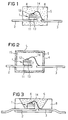
- the light-emitting semiconductor component of Figure 1 is the semiconductor body 1 by means of an electrically conductive connecting means, z. B. a metallic solder or an adhesive, with its rear contact 11 on a first electrical Port 2 attached.
- the front contact 12 is by means of a bonding wire 14 with a second electrical connection 3 connected.
- the free surfaces of the semiconductor body 1 and partial areas the electrical connections 2 and 3 are directly from one hardened, wavelength-converting potting compound 5 enclosed.
- This preferably has: epoxy casting resin 80-90% by weight, Fluorescent pigments (YAG: Ce) ⁇ 15% by weight, diethylene glycol monomethyl ether ⁇ 2% by weight, Tegoprene 6875-45 ⁇ 2% by weight, Aerosil 200 ⁇ 5 wt%
- FIG. 2 of an inventive Semiconductor device differs from that of Figure 1 in that the semiconductor body 1 and portions of electrical connections 2 and 3 instead of a wavelength converting one Potting compound from a transparent Envelope 15 are enclosed.
- This transparent envelope 15 causes no change in the wavelength of the semiconductor body 1 emitted radiation and consists for example of one Epoxy, silicone, commonly used in LED technology or acrylic resin or any other suitable radiation-permeable material such.
- a layer 4 is applied to this transparent covering 15, made of a wavelength-converting casting compound, as shown in Figure 2, the entire surface of the envelope 15 covered. It is also conceivable that the layer 4 only covered a portion of this surface.
- Layer 4 exists for example from a transparent epoxy resin, the is mixed with phosphor particles 6. Also suitable here as a phosphor for a white glowing semiconductor component preferably YAG: Ce.
- "Prefabricated” means that the basic housing 8 already at the connections 2, 3, for example is finished by injection molding before the semiconductor body is mounted on connection 2.
- the basic housing 8 consists for example of an opaque plastic and the recess 9 is in terms of its shape as a reflector 17 for those emitted by the semiconductor body during operation Radiation (if necessary by suitable coating of the inside walls of the Recess 9) formed.
- Such basic housing 8 in particular for light-emitting diodes that can be surface-mounted on printed circuit boards used. You will be assembling the semiconductor body on a conductor strip having the electrical connections 2, 3 (Leadframe) e.g. B. applied by injection molding.
- the recess 9 is with a potting compound 5, the composition the above in connection with the description of FIG. 1 specified specified, filled.
- FIG. in this connection is the electroluminescent semiconductor body 1 in a as Reflector-formed part 16 of the first electrical connection 2 attached for example by soldering or gluing.
- Such housing designs are known in light-emitting diode technology and therefore require no further explanation.
- the free surfaces of the semiconductor body 1 are immediate covered with a potting compound 5 with phosphor particles 6, the again surrounded by a further transparent covering 10 is.
- FIG. 5 there is a layer 4 (possible materials as stated above) directly on the semiconductor body 1 applied.
- This and parts of the electrical Connections 2,3 are of another transparent Envelope 10 enclosed, which does not change the wavelength caused through the layer 4 radiation and for example from a usable in light emitting diode technology transparent epoxy resin or made of glass.
- the potting compound 5, possibly the transparent covering 15, and / or the further transparent covering 10 can advantageously have light-scattering particles, advantageously so-called diffusers.
- diffusers are mineral fillers, in particular CaF 2 , TiO 2 , SiO 2 , CaCO 3 or BaSO 4 or organic pigments. These materials can easily be added to epoxy resins.
- FIGS. 6, 7 and 8 show emission spectra of a blue one Light-emitting semiconductor body (Fig. 6) (luminescence maximum at ⁇ ⁇ 430 nm) or by means of such a semiconductor body manufactured white luminous semiconductor components (Figs. 7 and 8) shown. On the abscissa is the Wavelength ⁇ in nm and on the ordinate is a relative one Electroluminescence (EL) intensity applied.
- Fig. 6 blue one Light-emitting semiconductor body
- Figs. 7 and 8 show emission spectra of a blue one Light-emitting semiconductor body (Fig. 6) (luminescence maximum at ⁇ ⁇ 430 nm) or by means of such a semiconductor body manufactured white luminous semiconductor components (Figs. 7 and 8) shown.
- On the abscissa is the Wavelength ⁇ in nm and on the ordinate is a relative one Electroluminescence (EL) intensity applied.
- EL Electroluminescence
- the Dashed line 30 in Figure 7 represents an emission spectrum of a semiconductor device that emits radiation from two complementary Wavelength ranges (blue and yellow) and thus emits a total of white light.
- the emission spectrum shows here at wavelengths between approx. 400 and approx. 430 nm (blue) and a maximum between about 550 and about 580 nm (yellow).
- the solid line 31 represents the emission spectrum of a semiconductor device that has the color white from three wavelength ranges (Additive color triplet of blue, green and Red) mixes.
- the emission spectrum shows here, for example at the wavelengths of approx. 430 nm (blue), approx. 500 nm (green) and about 615 nm (red) each a maximum.
- FIG. 8 shows an emission spectrum of a white light
- Semiconductor component with an emission spectrum according to 6 emitting semiconductor body is provided and at which is used as the phosphor YAG: Ce. From that of the semiconductor body only a part of the radiation emitted according to FIG. 6 converted to a longer wavelength range, so that white light is created as a mixed color.
- the different dashed lines Lines 30 to 33 of Figure 8 represent emission spectra of semiconductor components according to the invention, in which the epoxy resin of the potting compound 5 different YAG: Ce concentrations having.
- FIG. 12 illustrates that in the inventive Semiconductor device in a simple manner by changing the Fluorescent concentration in the epoxy resin is the CIE color locus of the white Light can be changed.
Abstract
Description
Claims (37)
- Wellenlängenkonvertierende Vergußmasse (5) auf der Basis eines transparenten Epoxidgießharzes für ein elektrolumineszierendes Bauelement mit einem ultraviolettes, blaues oder grünes Licht aussendenden Körper (1), bei der im transparenten Epoxidgießharz ein anorganisches Leuchtstoffpigmentpulver mit Leuchtstoffpigmenten (6) aus der Gruppe der mit seltenen Erden dotierten Granate, mit seltenen Erden dotierten Thiogallate, mit seltenen Erden dotierten Aluminate und/oder mit seltenen Erden dotierten Orthosilikate dispergiert ist und die Leuchtstoffpigmente Korngrößen ≤ 20 µm und ein d50 ≤ 5 µm aufweisen.
- Vergußmasse nach Anspruch 1, bei der die Leuchtstoffpigmente (6) kugelförmig oder schuppenförmig sind.
- Vergußmasse nach Anspruch 1 oder 2, bei der der mittlere Korndurchmesser d50 der Leuchtstoffpigmente (6) zwischen 1 und 2 µm liegt.
- Vergußmasse nach einem der Ansprüche 1 bis 3, die zusammengesetzt ist aus:a) Epoxidgießharz ≥ 60 Gew%b) Leuchtstoffpigmente > 0 und ≤ 25 Gew%c) Thixotropiermittel > 0 und ≤ 10 Gew%d) mineralischem Diffusor > 0 und ≤ 10 Gew%e) Verarbeitungshilfsmittel > 0 und ≤ 3 Gew%f) Hydrophobiermittel > 0 und ≤ 3 Gew%g) Haftvermittler > 0 und ≤ 2 Gew%.
- Vergußmasse nach einem der Ansprüche 1 bis 4, bei der der Eisengehalt ≤ 20ppm ist.
- Vergußmasse nach einem der Ansprüche 1 bis 5, bei der die Leuchtstoffpigmente (6) mit einem Silikon-Coating versehen sind.
- Verfahren zum Herstellen einer Vergußmasse für ein elektrolumineszierendes Bauelement mit einem ultraviolettes, blaues oder grünes Licht aussendenden Körper (1), bei dem ein anorganisches Leuchtstoffpigmentpulver, mit Leuchtstoffpigmenten (6) aus der Gruppe der mit seltenen Erden dotierten Granate, mit seltenen Erden dotierten Thiogallate, mit seltenen Erden dotierten Aluminate und/oder mit seltenen Erden dotierten Orthosilikate, mit Korngrößen ≤ 20 µm und mit ein d50 ≤ 5 µm hergestellt wird und in der Vergussmasse dispergiert wird.
- Verfahren nach Anspruch 7, bei dem das Leuchtstoffpigmentpulver bei einer Temperatur ≥ 200°C getempert wird.
- Verfahren nach Anspruch 7 oder 8, bei dem das Leuchtstoffpigmentpulver in einem höher siedenden Alkohol geschlämmt und anschließend getrocknet wird.
- Verfahren nach einem der Ansprüche 7 bis 9, bei dem dem Leuchtstoffpigmentpulver ein hydrophobierendes Silikonwachs zugegeben wird.
- Verfahren nach einem der Ansprüche 7 bis 10, bei dem das Leuchstoffpigmentpulver mit Alkoholen, Glykolethern und Silikonen bei erhöhten Temperaturen oberflächenmodifiziert wird.
- Verfahren nach einem der Ansprüche 7 bis 11, bei dem ein Leuchtstoffpigmentpulver mit einem mittleren Korndurchmesser d50 zwischen 1 und 2 µm hergestellt wird.
- Verfahren nach einem der Ansprüche 7 bis 12, bei dema) Epoxidgießharz ≥ 60 Gew%b) Leuchtstoffpigmente > 0 und ≤ 25 Gew%c) Thixotropiermittel > 0 und ≤ 10 Gew%d) mineralischem Diffusor > 0 und ≤ 10 Gew%e) Verarbeitungshilfsmittel > 0 und ≤ 3 Gew%f) Hydrophobiermittel > 0 und ≤ 3 Gew%g) Haftvermittler > 0 und ≤ 2 Gew% vermischt werden.
- Verfahren nach einem der Ansprüche 7 bis 13, bei dem die Leuchtstoffpigmente (6) mit einem Silikon-Coating versehen werden.
- Verfahren zum Herstellen eines lichtabstrahlenden Halbleiterbauelements, bei dem ein Halbleiterkörper (1), der eine Halbleiterschichtenfolge (7) aufweist, die geeignet ist, im Betrieb des Halbleiterbauelements elektromagnetische Strahlung aus dem ultravioletten, blauen und/oder grünen Spektralbereich auszusenden, zumindest teilweise mit einer Vergußmasse gemäß einem der Patentansprüche 1 bis 6 bzw. mit einer nach einem Verfahren gemäß einem der Ansprüche 7 bis 14 hergestellten Vergußmasse umschlossen wird.
- Verfahren zum Herstellen eines lichtabstrahlenden Halbleiterbauelements, bei dem auf einen Halbleiterkörper (1), der eine Halbleiterschichtenfolge (7) aufweist, die geeignet ist, im Betrieb des Halbleiterbauelements elektromagnetische Strahlung aus dem ultravioletten, blauen und/oder grünen Spektralbereich auszusenden, eine Schicht (4) aus einer Vergußmasse gemäß einem der Patentansprüche 1 bis 6 bzw. aus einer nach einem Verfahren gemäß einem der Ansprüche 7 bis 14 hergestellten Vergußmasse aufgebracht wird und der Halbleiterkörper (1) in ein SMD-Gehäuse oder ein Radial-Gehäuse montiert wird.
- Lichtabstrahlendes Halbleiterbauelement, hergestellt mit einer wellenlängenkonvertierenden Vergußmasse nach einem der Ansprüche 1 bis 6 bzw. mit einer nach einem Verfahren gemäß einem der Ansprüche 7 bis 14 hergestellten Vergußmasse, mit einem Halbleiterkörper (1), der eine Halbleiterschichtenfolge (7) aufweist, die geeignet ist, im Betrieb des Halbleiterbauelements elektromagnetische Strahlung aus dem ultravioletten, blauen und/oder grünen Spektralbereich auszusenden, und die Leuchtstoffpigmente einen Teil der aus diesem Spektralbereich stammenden Strahlung in Strahlung mit größerer Wellenlänge umwandelt, derart, daß das Halbleiterbauelement Mischstrahlung, insbesondere mischfarbiges Licht, bestehend aus dieser Strahlung und aus Strahlung aus dem ultravioletten, blauen und/oder grünen Spektralbereich aussendet.
- Lichtabstrahlendes Halbleiterbauelement nach Anspruch 17, bei dem die Vergußmasse zumindest einen Teil des Halbleiterkörpers (1) umschließt.
- Lichtabstrahlendes Halbleiterbauelement nach Anspruch 17 oder 18, bei dem das vom Halbleiterkörper (1) ausgesandte Strahlungsspektrum bei einer Wellenlänge kleiner oder gleich 520 nm ein Intensitätsmaximum aufweist und ein von den Leuchtstoffpigmenten spektral selektiv absorbierter Wellenlängenbereich außerhalb dieses Intensitätsmaximums liegt.
- Lichtabstrahlendes Halbleiterbauelement nach Anspruch 17 oder 18, bei dem das vom Halbleiterkörper (1) ausgesandte Strahlungsspektrum bei einer Wellenlänge zwischen 420nm und 460 nm ein Intensitätsmaximum aufweist.
- Lichtabstrahlendes Halbleiterbauelement nach Anspruch 17 oder 18, bei dem das vom Halbleiterkörper (1) ausgesandte Strahlungsspektrum bei 430 nm oder 450 nm ein Intensitätsmaximum aufweist.
- Lichtabstrahlendes Halbleiterbauelement nach Anspruch 19, 20 oder 21, bei dem der Halbleiterkörper auf der Basis von GaxAl1-xN oder auf der Basis von GaxIn1-xN hergestellt ist.
- Lichtabstrahlendes Halbleiterbauelement nach einem der Ansprüche 17 bis 22, bei dem in der Vergußmasse (5) mehrere verschiedene Leuchtstoffpartikelarten, die bei unterschiedlichen Wellenlängen emittieren, dispergiert sind.
- Lichtabstrahlendes Halbleiterbauelement nach einem der Ansprüche 17 bis 22, bei dem die Vergußmasse (5) hinsichtlich Wirtsgitter und Art und Ausmaß der Dotierung mit verschiedenartigen Leuchtstoffpigmenten (6) versehen ist.
- Lichtabstrahlendes Halbleiterbauelement nach einem der Ansprüche 17 bis 24, bei dem der Halbleiterkörper (1) in einer Ausnehmung (9) eines Grundgehäuses (8) angeordnet ist und daß die Ausnehmung (9) zumindest teilweise mit der Vergußmasse (5) gefüllt ist.
- Lichtabstrahlendes Halbleiterbauelement nach einem der Ansprüche 17 bis 24, bei dem der Halbleiterkörper (1) in einem als Reflektor ausgebildeten Teil (16) eines elektrischen Anschlusses (2) befestigt ist, der zumindest teilweise mit der Vergußmasse (5) gefüllt ist.
- Lichtabstrahlendes Halbleiterbauelement nach einem der Ansprüche 17 bis 24, bei dem auf dem Halbleiterkörper (1) eine Schicht (4) aus der Vergußmasse aufgebracht ist.
- Lichtabstrahlendes Halbleiterbauelement nach einem der Ansprüche 25 bis 27, bei dem die freien Oberflächen des Halbleiterkörpers (1) mit der Vergußmasse (5) bedeckt sind, auf der wiederum eine weitere transparente Umhüllung (10) aufgebracht ist.
- Lichtabstrahlendes Halbleiterbauelement nach einem der Ansprüche 17 bis 28, das weißes Licht aussendet, indem der Halbleiterkörper blaue Strahlung aussendet und der Leuchtstoff blaue Strahlung in gelbe Strahlung umwandelt.
- Lichtabstrahlendes Halbleiterbauelement nach Anspruch 29, bei dem das Emissionsspektrum zwischen ca. 400 und ca. 430 nm und zwischen ca. 550 und ca. 580 nm je ein Maximum aufweist.
- Lichtabstrahlendes Halbleiterbauelement nach einem der Ansprüche 17 bis 28, das weißes Licht aussendet, indem der Halbleiterkörper blaue Strahlung aussendet und der Leuchtstoff blaue Strahlung in grüne und in rote Strahlung umwandelt.
- Lichtabstrahlendes Halbleiterbauelement nach Anspruch 31, bei dem das Emissionsspektrum bei ca. 430 nm, bei ca. 500 nm und bei ca. 615 nm je ein Maximum aufweist.
- Lichtabstrahlendes Halbleiterbauelement nach einem der Ansprüche 17 bis 32, bei dem der Vergußmasse zusätzlich lichtstreuende Partikel zugesetzt sind.
- Lichtabstrahlendes Halbleiterbauelement nach Anspruch 28, bei dem der transparenten Umhüllung (10) lichtstreuende Partikel zugesetzt sind.
- Lichtabstrahlendes Halbleiterbauelement nach einem der Ansprüche 17 bis 34, bei dem der Halbleiterkörper neben einer sichtbaren Strahlung ultraviolette Strahlung aussendet, die von der Vergußmasse in sichtbare Strahlung umgewandelt wird.
- Halbleiterkörper (1), der eine Halbleiterschichtenfolge (7) aufweist, die geeignet ist, im Betrieb des Halbleiterbauelements elektromagnetische Strahlung aus dem ultravioletten, blauen und/oder grünen Spektralbereich auszusenden, auf dem eine Schicht (4) aus einer Vergußmasse gemäß einem der Patentansprüche 1 bis 6 bzw. aus einer nach einem Verfahren gemäß einem der Ansprüche 7 bis 14 hergestellten Vergußmasse aufgebracht ist.
- Halbleiterkörper nach Anspruch 36, der auf der Basis von GaxAl1-xN oder auf der Basis von GaxIn1-xN hergestellt ist.
Applications Claiming Priority (3)
| Application Number | Priority Date | Filing Date | Title |
|---|---|---|---|
| DE19638667A DE19638667C2 (de) | 1996-09-20 | 1996-09-20 | Mischfarbiges Licht abstrahlendes Halbleiterbauelement mit Lumineszenzkonversionselement |
| DE19638667 | 1996-09-20 | ||
| EP97909167A EP0862794B1 (de) | 1996-09-20 | 1997-09-22 | Wellenlängenkonvertierende vergussmasse und verfahren zu deren herstellung, verfahren zum herstellen eines licht abstrahlenden halbleiterbauelements und licht abstrahlendes halbleiterbauelement |
Related Parent Applications (2)
| Application Number | Title | Priority Date | Filing Date |
|---|---|---|---|
| EP97909167A Division EP0862794B1 (de) | 1996-09-20 | 1997-09-22 | Wellenlängenkonvertierende vergussmasse und verfahren zu deren herstellung, verfahren zum herstellen eines licht abstrahlenden halbleiterbauelements und licht abstrahlendes halbleiterbauelement |
| EP97909167.5 Division | 1998-03-26 |
Publications (3)
| Publication Number | Publication Date |
|---|---|
| EP1221724A2 true EP1221724A2 (de) | 2002-07-10 |
| EP1221724A3 EP1221724A3 (de) | 2005-07-06 |
| EP1221724B1 EP1221724B1 (de) | 2011-02-16 |
Family
ID=7806400
Family Applications (2)
| Application Number | Title | Priority Date | Filing Date |
|---|---|---|---|
| EP02007512A Revoked EP1221724B1 (de) | 1996-09-20 | 1997-09-22 | Wellenlängenkonvertierende Vergussmasse, deren Verwendung und Verfahren zu deren Herstellung |
| EP97909167A Expired - Lifetime EP0862794B1 (de) | 1996-09-20 | 1997-09-22 | Wellenlängenkonvertierende vergussmasse und verfahren zu deren herstellung, verfahren zum herstellen eines licht abstrahlenden halbleiterbauelements und licht abstrahlendes halbleiterbauelement |
Family Applications After (1)
| Application Number | Title | Priority Date | Filing Date |
|---|---|---|---|
| EP97909167A Expired - Lifetime EP0862794B1 (de) | 1996-09-20 | 1997-09-22 | Wellenlängenkonvertierende vergussmasse und verfahren zu deren herstellung, verfahren zum herstellen eines licht abstrahlenden halbleiterbauelements und licht abstrahlendes halbleiterbauelement |
Country Status (8)
| Country | Link |
|---|---|
| US (9) | US6066861A (de) |
| EP (2) | EP1221724B1 (de) |
| JP (10) | JP3364229B2 (de) |
| KR (8) | KR101301650B1 (de) |
| CN (8) | CN101081909B (de) |
| BR (1) | BR9706787A (de) |
| DE (6) | DE19638667C2 (de) |
| WO (1) | WO1998012757A1 (de) |
Cited By (8)
| Publication number | Priority date | Publication date | Assignee | Title |
|---|---|---|---|---|
| WO2004040661A3 (de) * | 2002-10-30 | 2004-09-10 | Osram Opto Semiconductors Gmbh | Verfahren zum herstellen einer leuchtdioden-lichtquelle mit lumineszenz-konversionselement |
| US7157745B2 (en) | 2004-04-09 | 2007-01-02 | Blonder Greg E | Illumination devices comprising white light emitting diodes and diode arrays and method and apparatus for making them |
| WO2007104665A1 (de) * | 2006-03-13 | 2007-09-20 | Osram Gesellschaft mit beschränkter Haftung | Hochbeständiges kunststoffbauteil, das zur lumineszenz geeignet ist |
| US7528421B2 (en) | 2003-05-05 | 2009-05-05 | Lamina Lighting, Inc. | Surface mountable light emitting diode assemblies packaged for high temperature operation |
| CN100508221C (zh) * | 2002-10-30 | 2009-07-01 | 奥斯兰姆奥普托半导体有限责任公司 | 用于混合色的发光二极管光源的生产方法 |
| US7696690B2 (en) | 2002-12-25 | 2010-04-13 | Japan Science And Technolgoy Agency | Short-wavelength light-emitting element arranged in a container with a window having a window board formed of a calcium fluoride crystals |
| WO2010045915A1 (de) * | 2008-10-22 | 2010-04-29 | Osram Opto Semiconductors Gmbh | Verfahren zum herstellen eines lumineszenzkonversionselements, lumineszenzkonversionselement und optoelektronisches bauteil |
| WO2018019846A1 (de) * | 2016-07-28 | 2018-02-01 | Osram Opto Semiconductors Gmbh | Strahlungsemittierender halbleiterchip, verfahren zur herstellung einer vielzahl strahlungsemittierender halbleiterchips, strahlungsemittierendes bauelement und verfahren zur herstellung eines strahlungsemittierenden bauelements |
Families Citing this family (885)
| Publication number | Priority date | Publication date | Assignee | Title |
|---|---|---|---|---|
| DE19638667C2 (de) * | 1996-09-20 | 2001-05-17 | Osram Opto Semiconductors Gmbh | Mischfarbiges Licht abstrahlendes Halbleiterbauelement mit Lumineszenzkonversionselement |
| BRPI9715293B1 (pt) * | 1996-06-26 | 2016-11-01 | Osram Ag | elemento de cobertura para um elemento de construção optoeletrônico |
| TW383508B (en) * | 1996-07-29 | 2000-03-01 | Nichia Kagaku Kogyo Kk | Light emitting device and display |
| US6613247B1 (en) * | 1996-09-20 | 2003-09-02 | Osram Opto Semiconductors Gmbh | Wavelength-converting casting composition and white light-emitting semiconductor component |
| JP3378465B2 (ja) * | 1997-05-16 | 2003-02-17 | 株式会社東芝 | 発光装置 |
| US6623670B2 (en) | 1997-07-07 | 2003-09-23 | Asahi Rubber Inc. | Method of molding a transparent coating member for light-emitting diodes |
| US6319425B1 (en) * | 1997-07-07 | 2001-11-20 | Asahi Rubber Inc. | Transparent coating member for light-emitting diodes and a fluorescent color light source |
| AU747260B2 (en) | 1997-07-25 | 2002-05-09 | Nichia Chemical Industries, Ltd. | Nitride semiconductor device |
| EP1004145B1 (de) * | 1997-07-29 | 2005-06-01 | Osram Opto Semiconductors GmbH | Optoelektronisches bauelement |
| US6806659B1 (en) * | 1997-08-26 | 2004-10-19 | Color Kinetics, Incorporated | Multicolored LED lighting method and apparatus |
| US7014336B1 (en) * | 1999-11-18 | 2006-03-21 | Color Kinetics Incorporated | Systems and methods for generating and modulating illumination conditions |
| US7161313B2 (en) | 1997-08-26 | 2007-01-09 | Color Kinetics Incorporated | Light emitting diode based products |
| US20030133292A1 (en) | 1999-11-18 | 2003-07-17 | Mueller George G. | Methods and apparatus for generating and modulating white light illumination conditions |
| US7038398B1 (en) * | 1997-08-26 | 2006-05-02 | Color Kinetics, Incorporated | Kinetic illumination system and methods |
| US6252254B1 (en) | 1998-02-06 | 2001-06-26 | General Electric Company | Light emitting device with phosphor composition |
| US6255670B1 (en) * | 1998-02-06 | 2001-07-03 | General Electric Company | Phosphors for light generation from light emitting semiconductors |
| US6294800B1 (en) | 1998-02-06 | 2001-09-25 | General Electric Company | Phosphors for white light generation from UV emitting diodes |
| US6580097B1 (en) * | 1998-02-06 | 2003-06-17 | General Electric Company | Light emitting device with phosphor composition |
| JP3541709B2 (ja) * | 1998-02-17 | 2004-07-14 | 日亜化学工業株式会社 | 発光ダイオードの形成方法 |
| EP1089335A4 (de) * | 1998-05-20 | 2002-02-06 | Rohm Co Ltd | Halbleitervorrichtung |
| DE19829197C2 (de) | 1998-06-30 | 2002-06-20 | Siemens Ag | Strahlungsaussendendes und/oder -empfangendes Bauelement |
| JP2002520822A (ja) | 1998-06-30 | 2002-07-09 | オスラム オプト セミコンダクターズ ゲゼルシャフト ミット ベシュレンクテル ハフツング ウント コンパニー オッフェネ ハンデルスゲゼルシャフト | 可視光を発生する光源 |
| US5959316A (en) * | 1998-09-01 | 1999-09-28 | Hewlett-Packard Company | Multiple encapsulation of phosphor-LED devices |
| CN1227749C (zh) † | 1998-09-28 | 2005-11-16 | 皇家菲利浦电子有限公司 | 照明系统 |
| US6429583B1 (en) | 1998-11-30 | 2002-08-06 | General Electric Company | Light emitting device with ba2mgsi2o7:eu2+, ba2sio4:eu2+, or (srxcay ba1-x-y)(a1zga1-z)2sr:eu2+phosphors |
| JP2000208822A (ja) * | 1999-01-11 | 2000-07-28 | Matsushita Electronics Industry Corp | 半導体発光装置 |
| JP3770014B2 (ja) | 1999-02-09 | 2006-04-26 | 日亜化学工業株式会社 | 窒化物半導体素子 |
| US6351069B1 (en) | 1999-02-18 | 2002-02-26 | Lumileds Lighting, U.S., Llc | Red-deficiency-compensating phosphor LED |
| US6680569B2 (en) | 1999-02-18 | 2004-01-20 | Lumileds Lighting U.S. Llc | Red-deficiency compensating phosphor light emitting device |
| EP1168539B1 (de) | 1999-03-04 | 2009-12-16 | Nichia Corporation | Nitridhalbleiterlaserelement |
| DE19918370B4 (de) | 1999-04-22 | 2006-06-08 | Osram Opto Semiconductors Gmbh | LED-Weißlichtquelle mit Linse |
| JP3458823B2 (ja) * | 1999-05-11 | 2003-10-20 | 日亜化学工業株式会社 | 面発光装置 |
| KR100661945B1 (ko) * | 1999-06-14 | 2006-12-28 | 후-쿠 후앙 | 광 입사에 의해 활성화되는 에너지 레벨 전이에 기초하는 전자기파 방사 장치 및 방법 |
| DE19934126A1 (de) * | 1999-07-23 | 2001-01-25 | Patent Treuhand Ges Fuer Elektrische Gluehlampen Mbh | Leuchtstoff für Lichtquellen und zugehörige Lichtquelle |
| DE19951790A1 (de) * | 1999-10-27 | 2001-05-03 | Patent Treuhand Ges Fuer Elektrische Gluehlampen Mbh | Leuchtstoff für Lichtquellen und zugehörige Lichtquelle |
| CN100334746C (zh) | 1999-07-23 | 2007-08-29 | 奥斯兰姆奥普托半导体股份有限两合公司 | 荧光材料混合物、波长转换的浇注料和光源装置 |
| CN1190997C (zh) * | 1999-07-23 | 2005-02-23 | 电灯专利信托有限公司 | 光源的发光物质及其相关的光源 |
| US6686691B1 (en) * | 1999-09-27 | 2004-02-03 | Lumileds Lighting, U.S., Llc | Tri-color, white light LED lamps |
| KR100683364B1 (ko) | 1999-09-27 | 2007-02-15 | 필립스 루미리즈 라이팅 캄파니 엘엘씨 | 완전한 형광 물질 변환에 의해 백색광을 생성하는 발광다이오드 소자 |
| US6696703B2 (en) * | 1999-09-27 | 2004-02-24 | Lumileds Lighting U.S., Llc | Thin film phosphor-converted light emitting diode device |
| DE19947044B9 (de) * | 1999-09-30 | 2007-09-13 | Osram Opto Semiconductors Gmbh | Oberflächenmontierbares optoelektronisches Bauelement mit Reflektor und Verfahren zur Herstellung desselben |
| JP2001111109A (ja) * | 1999-10-07 | 2001-04-20 | Sharp Corp | 窒化ガリウム系化合物半導体発光素子 |
| DE19952712A1 (de) * | 1999-11-02 | 2001-05-10 | Osram Opto Semiconductors Gmbh | Laserdiodenvorrichtung |
| DE19952932C1 (de) * | 1999-11-03 | 2001-05-03 | Osram Opto Semiconductors Gmbh | LED-Weißlichtquelle mit breitbandiger Anregung |
| JP2003517705A (ja) * | 1999-11-18 | 2003-05-27 | カラー・キネティックス・インコーポレーテッド | 照明状態を発生し且つ調整するシステム及び方法 |
| US20020176259A1 (en) * | 1999-11-18 | 2002-11-28 | Ducharme Alfred D. | Systems and methods for converting illumination |
| US7202506B1 (en) | 1999-11-19 | 2007-04-10 | Cree, Inc. | Multi element, multi color solid state LED/laser |
| JP3895086B2 (ja) * | 1999-12-08 | 2007-03-22 | ローム株式会社 | チップ型半導体発光装置 |
| JP2001177153A (ja) * | 1999-12-17 | 2001-06-29 | Sharp Corp | 発光装置 |
| JP2001177145A (ja) * | 1999-12-21 | 2001-06-29 | Toshiba Electronic Engineering Corp | 半導体発光素子およびその製造方法 |
| DE19963805B4 (de) * | 1999-12-30 | 2005-01-27 | Osram Opto Semiconductors Gmbh | Weißlichtquelle auf der Basis nichtlinear-optischer Prozesse |
| DE19964252A1 (de) | 1999-12-30 | 2002-06-06 | Osram Opto Semiconductors Gmbh | Oberflächenmontierbares Bauelement für eine LED-Weißlichtquelle |
| TWI273722B (en) * | 2000-01-27 | 2007-02-11 | Gen Electric | Organic light emitting device and method for mounting |
| JP4709458B2 (ja) | 2000-02-23 | 2011-06-22 | オスラム オプト セミコンダクターズ ゲゼルシャフト ミット ベシュレンクテル ハフツング | 光ルミネセンス層およびその形成方法 |
| DE10010638A1 (de) * | 2000-03-03 | 2001-09-13 | Osram Opto Semiconductors Gmbh | Verfahren zur Herstellung eines lichtabstrahlenden Halbleiterkörpers mit Lumineszenzkonversionselement |
| JP4406490B2 (ja) * | 2000-03-14 | 2010-01-27 | 株式会社朝日ラバー | 発光ダイオード |
| US6538371B1 (en) | 2000-03-27 | 2003-03-25 | The General Electric Company | White light illumination system with improved color output |
| US6409938B1 (en) | 2000-03-27 | 2002-06-25 | The General Electric Company | Aluminum fluoride flux synthesis method for producing cerium doped YAG |
| US6522065B1 (en) | 2000-03-27 | 2003-02-18 | General Electric Company | Single phosphor for creating white light with high luminosity and high CRI in a UV led device |
| US6603258B1 (en) * | 2000-04-24 | 2003-08-05 | Lumileds Lighting, U.S. Llc | Light emitting diode device that emits white light |
| DE10020465A1 (de) | 2000-04-26 | 2001-11-08 | Osram Opto Semiconductors Gmbh | Strahlungsemittierendes Halbleiterbauelement mit Lumineszenzkonversionselement |
| US6604971B1 (en) | 2000-05-02 | 2003-08-12 | General Electric Company | Fabrication of LED lamps by controlled deposition of a suspension media |
| EP1153792A1 (de) * | 2000-05-09 | 2001-11-14 | SIDLER GMBH & CO | Leuchtenanordnung mit mehreren LED's |
| US6501100B1 (en) * | 2000-05-15 | 2002-12-31 | General Electric Company | White light emitting phosphor blend for LED devices |
| US6621211B1 (en) * | 2000-05-15 | 2003-09-16 | General Electric Company | White light emitting phosphor blends for LED devices |
| US6555958B1 (en) | 2000-05-15 | 2003-04-29 | General Electric Company | Phosphor for down converting ultraviolet light of LEDs to blue-green light |
| US6466135B1 (en) | 2000-05-15 | 2002-10-15 | General Electric Company | Phosphors for down converting ultraviolet light of LEDs to blue-green light |
| GB0012377D0 (en) * | 2000-05-22 | 2000-07-12 | Isis Innovation | Oxide based phosphors |
| DE10026435A1 (de) | 2000-05-29 | 2002-04-18 | Osram Opto Semiconductors Gmbh | Kalzium-Magnesium-Chlorosilikat-Leuchtstoff und seine Anwendung bei Lumineszenz-Konversions-LED |
| US6504179B1 (en) | 2000-05-29 | 2003-01-07 | Patent-Treuhand-Gesellschaft Fur Elektrische Gluhlampen Mbh | Led-based white-emitting illumination unit |
| DE10027206A1 (de) * | 2000-05-31 | 2001-12-13 | Osram Opto Semiconductors Gmbh | Alterungsstabile Epoxidharzsysteme, daraus hergestellte Formstoffe und Bauelemente und deren Verwendung |
| JP2002190622A (ja) * | 2000-12-22 | 2002-07-05 | Sanken Electric Co Ltd | 発光ダイオード用透光性蛍光カバー |
| KR100869866B1 (ko) | 2000-06-29 | 2008-11-24 | 코닌클리즈케 필립스 일렉트로닉스 엔.브이. | 광전 소자 및 그 피복 방법 |
| DE10032453A1 (de) * | 2000-07-04 | 2002-01-24 | Vishay Semiconductor Gmbh | Strahlung emittierendes Bauelement |
| DE10036940A1 (de) | 2000-07-28 | 2002-02-07 | Patent Treuhand Ges Fuer Elektrische Gluehlampen Mbh | Lumineszenz-Konversions-LED |
| JP2002050797A (ja) * | 2000-07-31 | 2002-02-15 | Toshiba Corp | 半導体励起蛍光体発光装置およびその製造方法 |
| US6747406B1 (en) * | 2000-08-07 | 2004-06-08 | General Electric Company | LED cross-linkable phospor coating |
| EP1179858B1 (de) * | 2000-08-09 | 2009-03-18 | Avago Technologies General IP (Singapore) Pte. Ltd | Lichtemittierende Vorrichtungen |
| US6635363B1 (en) * | 2000-08-21 | 2003-10-21 | General Electric Company | Phosphor coating with self-adjusting distance from LED chip |
| JP2002076434A (ja) * | 2000-08-28 | 2002-03-15 | Toyoda Gosei Co Ltd | 発光装置 |
| EP1187226B1 (de) * | 2000-09-01 | 2012-12-26 | Citizen Electronics Co., Ltd. | Oberflächenmontierbare LED und Herstellungsverfahren dafür |
| US6614103B1 (en) * | 2000-09-01 | 2003-09-02 | General Electric Company | Plastic packaging of LED arrays |
| JP2002141556A (ja) | 2000-09-12 | 2002-05-17 | Lumileds Lighting Us Llc | 改良された光抽出効果を有する発光ダイオード |
| JP3609709B2 (ja) * | 2000-09-29 | 2005-01-12 | 株式会社シチズン電子 | 発光ダイオード |
| US6998281B2 (en) * | 2000-10-12 | 2006-02-14 | General Electric Company | Solid state lighting device with reduced form factor including LED with directional emission and package with microoptics |
| US6650044B1 (en) * | 2000-10-13 | 2003-11-18 | Lumileds Lighting U.S., Llc | Stenciling phosphor layers on light emitting diodes |
| JP2002133925A (ja) * | 2000-10-25 | 2002-05-10 | Sanken Electric Co Ltd | 蛍光カバー及び半導体発光装置 |
| JP2002141559A (ja) * | 2000-10-31 | 2002-05-17 | Sanken Electric Co Ltd | 発光半導体チップ組立体及び発光半導体リードフレーム |
| AT4889U1 (de) * | 2000-11-07 | 2001-12-27 | Binder Co Ag | Diodenlichtquelle für eine zeilenkamera |
| US6518600B1 (en) | 2000-11-17 | 2003-02-11 | General Electric Company | Dual encapsulation for an LED |
| JP3614776B2 (ja) | 2000-12-19 | 2005-01-26 | シャープ株式会社 | チップ部品型ledとその製造方法 |
| AT410266B (de) | 2000-12-28 | 2003-03-25 | Tridonic Optoelectronics Gmbh | Lichtquelle mit einem lichtemittierenden element |
| JP4545956B2 (ja) * | 2001-01-12 | 2010-09-15 | ローム株式会社 | 半導体装置、およびその製造方法 |
| DE10101554A1 (de) * | 2001-01-15 | 2002-08-01 | Osram Opto Semiconductors Gmbh | Lumineszenzdiode |
| MY131962A (en) * | 2001-01-24 | 2007-09-28 | Nichia Corp | Light emitting diode, optical semiconductor device, epoxy resin composition suited for optical semiconductor device, and method for manufacturing the same |
| JP2002232013A (ja) * | 2001-02-02 | 2002-08-16 | Rohm Co Ltd | 半導体発光素子 |
| US6541800B2 (en) * | 2001-02-22 | 2003-04-01 | Weldon Technologies, Inc. | High power LED |
| DE10109349B4 (de) * | 2001-02-27 | 2012-04-19 | Osram Opto Semiconductors Gmbh | Strahlungsemittierendes Halbleiterbauelement |
| JP2002261333A (ja) * | 2001-03-05 | 2002-09-13 | Toyoda Gosei Co Ltd | 発光装置 |
| JP2002270365A (ja) * | 2001-03-12 | 2002-09-20 | Nippon Hoso Kyokai <Nhk> | El素子 |
| DE10112542B9 (de) * | 2001-03-15 | 2013-01-03 | Osram Opto Semiconductors Gmbh | Strahlungsemittierendes optisches Bauelement |
| JP2002299698A (ja) * | 2001-03-30 | 2002-10-11 | Sumitomo Electric Ind Ltd | 発光装置 |
| JP2002314143A (ja) * | 2001-04-09 | 2002-10-25 | Toshiba Corp | 発光装置 |
| JP4101468B2 (ja) * | 2001-04-09 | 2008-06-18 | 豊田合成株式会社 | 発光装置の製造方法 |
| US6685852B2 (en) | 2001-04-27 | 2004-02-03 | General Electric Company | Phosphor blends for generating white light from near-UV/blue light-emitting devices |
| US6686676B2 (en) * | 2001-04-30 | 2004-02-03 | General Electric Company | UV reflectors and UV-based light sources having reduced UV radiation leakage incorporating the same |
| JP2002344029A (ja) * | 2001-05-17 | 2002-11-29 | Rohm Co Ltd | 発光ダイオードの色調調整方法 |
| US6616862B2 (en) * | 2001-05-21 | 2003-09-09 | General Electric Company | Yellow light-emitting halophosphate phosphors and light sources incorporating the same |
| US6989412B2 (en) * | 2001-06-06 | 2006-01-24 | Henkel Corporation | Epoxy molding compounds containing phosphor and process for preparing such compositions |
| US6642652B2 (en) | 2001-06-11 | 2003-11-04 | Lumileds Lighting U.S., Llc | Phosphor-converted light emitting device |
| US6576488B2 (en) * | 2001-06-11 | 2003-06-10 | Lumileds Lighting U.S., Llc | Using electrophoresis to produce a conformally coated phosphor-converted light emitting semiconductor |
| JP4114331B2 (ja) * | 2001-06-15 | 2008-07-09 | 豊田合成株式会社 | 発光装置 |
| JP2002374007A (ja) * | 2001-06-15 | 2002-12-26 | Toyoda Gosei Co Ltd | 発光装置 |
| DE10131698A1 (de) * | 2001-06-29 | 2003-01-30 | Osram Opto Semiconductors Gmbh | Oberflächenmontierbares strahlungsemittierendes Bauelement und Verfahren zu dessen Herstellung |
| JP2003037295A (ja) * | 2001-07-05 | 2003-02-07 | Taiwan Lite On Electronics Inc | 発光ダイオードと発光ダイオードの製造方法 |
| DE10133352A1 (de) | 2001-07-16 | 2003-02-06 | Patent Treuhand Ges Fuer Elektrische Gluehlampen Mbh | Beleuchtungseinheit mit mindestens einer LED als Lichtquelle |
| JP2003027057A (ja) * | 2001-07-17 | 2003-01-29 | Hitachi Ltd | 光源およびそれを用いた画像表示装置 |
| DE10137641A1 (de) * | 2001-08-03 | 2003-02-20 | Osram Opto Semiconductors Gmbh | Hybrid-LED |
| TW511303B (en) * | 2001-08-21 | 2002-11-21 | Wen-Jr He | A light mixing layer and method |
| US6737681B2 (en) * | 2001-08-22 | 2004-05-18 | Nichia Corporation | Light emitting device with fluorescent member excited by semiconductor light emitting element |
| US7728345B2 (en) * | 2001-08-24 | 2010-06-01 | Cao Group, Inc. | Semiconductor light source for illuminating a physical space including a 3-dimensional lead frame |
| DE10142009B4 (de) * | 2001-08-28 | 2010-04-22 | Osram Opto Semiconductors Gmbh | LED - Lichtquelle mit einem Konversionsmittel und mit einer UV-absorbierenden Schicht |
| CN100423296C (zh) | 2001-09-03 | 2008-10-01 | 松下电器产业株式会社 | 半导体发光元件、发光装置及半导体发光元件的制造方法 |
| US7604361B2 (en) * | 2001-09-07 | 2009-10-20 | Litepanels Llc | Versatile lighting apparatus and associated kit |
| US6749310B2 (en) | 2001-09-07 | 2004-06-15 | Contrast Lighting Services, Inc. | Wide area lighting effects system |
| US7331681B2 (en) * | 2001-09-07 | 2008-02-19 | Litepanels Llc | Lighting apparatus with adjustable lenses or filters |
| DE10146719A1 (de) | 2001-09-20 | 2003-04-17 | Patent Treuhand Ges Fuer Elektrische Gluehlampen Mbh | Beleuchtungseinheit mit mindestens einer LED als Lichtquelle |
| DE10147040A1 (de) | 2001-09-25 | 2003-04-24 | Patent Treuhand Ges Fuer Elektrische Gluehlampen Mbh | Beleuchtungseinheit mit mindestens einer LED als Lichtquelle |
| DE20115914U1 (de) | 2001-09-27 | 2003-02-13 | Patent Treuhand Ges Fuer Elektrische Gluehlampen Mbh | Beleuchtungseinheit mit mindestens einer LED als Lichtquelle |
| JP3948650B2 (ja) | 2001-10-09 | 2007-07-25 | アバゴ・テクノロジーズ・イーシービーユー・アイピー(シンガポール)プライベート・リミテッド | 発光ダイオード及びその製造方法 |
| EP1437776B1 (de) * | 2001-10-12 | 2011-09-21 | Nichia Corporation | Lichtemittierendes bauelement und verfahren zu seiner herstellung |
| JP4043752B2 (ja) * | 2001-10-19 | 2008-02-06 | 星和電機株式会社 | 発光ダイオードランプとこれを用いた照明器具 |
| JP2003133595A (ja) * | 2001-10-24 | 2003-05-09 | Seiwa Electric Mfg Co Ltd | 発光ダイオードランプ、これに用いられる赤色蛍光体及びこれに用いられるフィルタ |
| US7858403B2 (en) * | 2001-10-31 | 2010-12-28 | Cree, Inc. | Methods and systems for fabricating broad spectrum light emitting devices |
| DE10153259A1 (de) | 2001-10-31 | 2003-05-22 | Osram Opto Semiconductors Gmbh | Optoelektronisches Bauelement |
| JP2003147351A (ja) * | 2001-11-09 | 2003-05-21 | Taiwan Lite On Electronics Inc | 白色光光源の製作方法 |
| US6734465B1 (en) * | 2001-11-19 | 2004-05-11 | Nanocrystals Technology Lp | Nanocrystalline based phosphors and photonic structures for solid state lighting |
| DE10241989A1 (de) | 2001-11-30 | 2003-06-18 | Osram Opto Semiconductors Gmbh | Optoelektronisches Bauelement |
| WO2003066374A2 (en) * | 2002-02-06 | 2003-08-14 | Schefenacker Vision Systems Usa Inc. | Center high mounted stop lamp including leds and tir lens |
| JP3972670B2 (ja) * | 2002-02-06 | 2007-09-05 | 豊田合成株式会社 | 発光装置 |
| US6881983B2 (en) * | 2002-02-25 | 2005-04-19 | Kopin Corporation | Efficient light emitting diodes and lasers |
| KR100961342B1 (ko) | 2002-03-22 | 2010-06-04 | 니치아 카가쿠 고교 가부시키가이샤 | 질화물 형광체와 그 제조 방법 및 발광 장치 |
| DE10213294B4 (de) * | 2002-03-25 | 2015-05-13 | Osram Gmbh | Verwendung eines UV-beständigen Polymers in der Optoelektronik sowie im Außenanwendungsbereich, UV-beständiges Polymer sowie optisches Bauelement |
| TW558065U (en) * | 2002-03-28 | 2003-10-11 | Solidlite Corp | Purplish pink light emitting diode |
| DE10214119A1 (de) * | 2002-03-28 | 2003-10-23 | Osram Opto Semiconductors Gmbh | Optoelektronisches Bauelement |
| US8294172B2 (en) | 2002-04-09 | 2012-10-23 | Lg Electronics Inc. | Method of fabricating vertical devices using a metal support film |
| US20030189215A1 (en) | 2002-04-09 | 2003-10-09 | Jong-Lam Lee | Method of fabricating vertical structure leds |
| US6911079B2 (en) * | 2002-04-19 | 2005-06-28 | Kopin Corporation | Method for reducing the resistivity of p-type II-VI and III-V semiconductors |
| TWI226357B (en) | 2002-05-06 | 2005-01-11 | Osram Opto Semiconductors Gmbh | Wavelength-converting reaction-resin, its production method, light-radiating optical component and light-radiating semiconductor-body |
| DE50309259D1 (de) * | 2002-05-06 | 2008-04-10 | Osram Opto Semiconductors Gmbh | Wellenlängenkonvertierende reaktionsharzmasse und leuchtdiodenbauelement |
| DE10221857A1 (de) * | 2002-05-16 | 2003-11-27 | Osram Opto Semiconductors Gmbh | Verfahren zum Befestigen eines Halbleiterchips in einem Kunststoffgehäusekörper, optoelektronisches Halbleiterbauelement und Verfahren zu dessen Herstellung |
| AU2003238234A1 (en) * | 2002-06-13 | 2003-12-31 | Cree, Inc. | Semiconductor emitter comprising a saturated phosphor |
| US7002180B2 (en) * | 2002-06-28 | 2006-02-21 | Kopin Corporation | Bonding pad for gallium nitride-based light-emitting device |
| US6734091B2 (en) | 2002-06-28 | 2004-05-11 | Kopin Corporation | Electrode for p-type gallium nitride-based semiconductors |
| WO2003107444A2 (en) | 2002-06-17 | 2003-12-24 | Kopin Corporation | Light-emitting diode device geometry |
| KR100567546B1 (ko) * | 2002-06-24 | 2006-04-05 | 서울반도체 주식회사 | 핑크색 발광 다이오드 및 그 제조 방법 |
| US6841802B2 (en) * | 2002-06-26 | 2005-01-11 | Oriol, Inc. | Thin film light emitting diode |
| DE10228634A1 (de) * | 2002-06-26 | 2004-01-22 | Osram Opto Semiconductors Gmbh | Oberflächenmontierbare Miniatur-Lumineszenz-und/oder Photo-Diode und Verfahren zu deren Herstellung |
| US6955985B2 (en) | 2002-06-28 | 2005-10-18 | Kopin Corporation | Domain epitaxy for thin film growth |
| US6809471B2 (en) * | 2002-06-28 | 2004-10-26 | General Electric Company | Phosphors containing oxides of alkaline-earth and Group-IIIB metals and light sources incorporating the same |
| KR101030068B1 (ko) | 2002-07-08 | 2011-04-19 | 니치아 카가쿠 고교 가부시키가이샤 | 질화물 반도체 소자의 제조방법 및 질화물 반도체 소자 |
| US7928455B2 (en) * | 2002-07-15 | 2011-04-19 | Epistar Corporation | Semiconductor light-emitting device and method for forming the same |
| US20040124433A1 (en) * | 2002-07-19 | 2004-07-01 | Kelly Stephen G. | Process for fabricating, and light emitting device resulting from, a homogenously mixed powder/pelletized compound |
| CN100595938C (zh) | 2002-08-01 | 2010-03-24 | 日亚化学工业株式会社 | 半导体发光元件及其制造方法、使用此的发光装置 |
| KR20040017926A (ko) * | 2002-08-22 | 2004-03-02 | 웬-치 호 | 광-혼합 층 및 광-혼합 방법 |
| US10340424B2 (en) * | 2002-08-30 | 2019-07-02 | GE Lighting Solutions, LLC | Light emitting diode component |
| JP2004128273A (ja) * | 2002-10-03 | 2004-04-22 | Sharp Corp | 発光素子 |
| JP2004132772A (ja) * | 2002-10-09 | 2004-04-30 | Casio Comput Co Ltd | 照明装置およびそれを用いた電子機器 |
| US7554258B2 (en) | 2002-10-22 | 2009-06-30 | Osram Opto Semiconductors Gmbh | Light source having an LED and a luminescence conversion body and method for producing the luminescence conversion body |
| DE10250911B4 (de) * | 2002-10-31 | 2009-08-27 | Osram Opto Semiconductors Gmbh | Verfahren zur Herstellung einer Umhüllung und/oder zumindest eines Teiles eines Gehäuses eines optoelektronischen Bauelements |
| JP2004158635A (ja) * | 2002-11-06 | 2004-06-03 | Stanley Electric Co Ltd | 表面実装型チップled及びその製造方法 |
| CN1980948B (zh) * | 2002-11-27 | 2011-08-10 | Dmi生物科学公司 | 治疗由增强磷酸化介导的疾病和病况 |
| DE10258193B4 (de) | 2002-12-12 | 2014-04-10 | Osram Opto Semiconductors Gmbh | Verfahren zum Herstellen von Leuchtdioden-Lichtquellen mit Lumineszenz-Konversionselement |
| US7042150B2 (en) * | 2002-12-20 | 2006-05-09 | Showa Denko K.K. | Light-emitting device, method of fabricating the device, and LED lamp using the device |
| DE10261908B4 (de) * | 2002-12-27 | 2010-12-30 | Osa Opto Light Gmbh | Verfahren zur Herstellung eines konversionslichtemittierenden Elementes auf der Basis von Halbleiterlichtquellen |
| DE10261672B4 (de) * | 2002-12-31 | 2005-11-24 | Osram Opto Semiconductors Gmbh | LED-Chip mit Konversionsstoff, optoelektronisches Bauelement mit einem derartigen LED-Chip und Verfahren zum Herstellen eines derartigen LED-Chips |
| JP3910144B2 (ja) * | 2003-01-06 | 2007-04-25 | シャープ株式会社 | 半導体発光装置およびその製造方法 |
| US7550777B2 (en) | 2003-01-10 | 2009-06-23 | Toyoda Gosei, Co., Ltd. | Light emitting device including adhesion layer |
| TWI351566B (en) | 2003-01-15 | 2011-11-01 | Semiconductor Energy Lab | Liquid crystal display device |
| US20040137656A1 (en) * | 2003-01-15 | 2004-07-15 | Gurbir Singh | Low thermal resistance light emitting diode package and a method of making the same |
| US20040142098A1 (en) * | 2003-01-21 | 2004-07-22 | Eastman Kodak Company | Using compacted organic materials in making white light emitting oleds |
| JP3717480B2 (ja) * | 2003-01-27 | 2005-11-16 | ローム株式会社 | 半導体発光装置 |
| US6982523B2 (en) * | 2003-01-28 | 2006-01-03 | Kabushiki Kaisha Fine Rubber Kenkyuusho | Red light emitting phosphor, its production and light emitting device |
| TWI237546B (en) | 2003-01-30 | 2005-08-01 | Osram Opto Semiconductors Gmbh | Semiconductor-component sending and/or receiving electromagnetic radiation and housing-basebody for such a component |
| US20040151829A1 (en) * | 2003-01-31 | 2004-08-05 | Eastman Kodak Company | Optimizing OLED emission |
| US7074346B2 (en) * | 2003-02-06 | 2006-07-11 | Ube Industries, Ltd. | Sialon-based oxynitride phosphor, process for its production, and use thereof |
| US7042020B2 (en) | 2003-02-14 | 2006-05-09 | Cree, Inc. | Light emitting device incorporating a luminescent material |
| CN103396933B (zh) | 2003-02-26 | 2016-04-20 | 凯利达基因组股份有限公司 | 通过杂交进行的随机阵列dna分析 |
| EP2262006A3 (de) * | 2003-02-26 | 2012-03-21 | Cree, Inc. | Weisslichtquelle mit Leuchtdiode und Leuchtstoffe |
| US7423296B2 (en) | 2003-02-26 | 2008-09-09 | Avago Technologies Ecbu Ip Pte Ltd | Apparatus for producing a spectrally-shifted light output from a light emitting device utilizing thin-film luminescent layers |
| JP2004260111A (ja) * | 2003-02-27 | 2004-09-16 | Sharp Corp | 半導体発光素子およびその半導体発光素子を用いた半導体発光装置 |
| DE10308890A1 (de) * | 2003-02-28 | 2004-09-09 | Opto Tech Corporation | Gehäusestruktur für eine Lichtemissionsdiode und Verfahren zu dessen Herstellung |
| DE10308866A1 (de) | 2003-02-28 | 2004-09-09 | Osram Opto Semiconductors Gmbh | Beleuchtungsmodul und Verfahren zu dessen Herstellung |
| JP4131178B2 (ja) * | 2003-02-28 | 2008-08-13 | 豊田合成株式会社 | 発光装置 |
| US6806658B2 (en) * | 2003-03-07 | 2004-10-19 | Agilent Technologies, Inc. | Method for making an LED |
| US6885033B2 (en) * | 2003-03-10 | 2005-04-26 | Cree, Inc. | Light emitting devices for light conversion and methods and semiconductor chips for fabricating the same |
| KR101100467B1 (ko) * | 2003-03-13 | 2011-12-29 | 오스람 옵토 세미컨덕터스 게엠베하 | 인광 효과를 가진 발광 변환 led 및 상기 led의 사용 방법 |
| DE10314524A1 (de) | 2003-03-31 | 2004-10-28 | Osram Opto Semiconductors Gmbh | Scheinwerfer und Scheinwerferelement |
| US7279832B2 (en) * | 2003-04-01 | 2007-10-09 | Innovalight, Inc. | Phosphor materials and illumination devices made therefrom |
| US20040252488A1 (en) * | 2003-04-01 | 2004-12-16 | Innovalight | Light-emitting ceiling tile |
| DE10315133A1 (de) * | 2003-04-03 | 2004-10-14 | Hella Kg Hueck & Co. | Beleuchtungseinheit für Kraftfahrzeuge |
| DE10316769A1 (de) * | 2003-04-10 | 2004-10-28 | Patent-Treuhand-Gesellschaft für elektrische Glühlampen mbH | Leuchtstoffbassierte LED und zugehöriger Leuchtstoff |
| US7125501B2 (en) * | 2003-04-21 | 2006-10-24 | Sarnoff Corporation | High efficiency alkaline earth metal thiogallate-based phosphors |
| US7368179B2 (en) * | 2003-04-21 | 2008-05-06 | Sarnoff Corporation | Methods and devices using high efficiency alkaline earth metal thiogallate-based phosphors |
| JP2006525682A (ja) * | 2003-04-30 | 2006-11-09 | クリー インコーポレイテッド | 高出力固体発光素子パッケージ |
| US7005679B2 (en) * | 2003-05-01 | 2006-02-28 | Cree, Inc. | Multiple component solid state white light |
| US7633093B2 (en) | 2003-05-05 | 2009-12-15 | Lighting Science Group Corporation | Method of making optical light engines with elevated LEDs and resulting product |
| US7777235B2 (en) | 2003-05-05 | 2010-08-17 | Lighting Science Group Corporation | Light emitting diodes with improved light collimation |
| US6982045B2 (en) * | 2003-05-17 | 2006-01-03 | Phosphortech Corporation | Light emitting device having silicate fluorescent phosphor |
| DE10323857A1 (de) * | 2003-05-26 | 2005-01-27 | Osram Opto Semiconductors Gmbh | Gehäuse für ein Laserdiodenbauelement, Laserdiodenbauelement und Verfahren zum Herstellen eines Laserdiodenbauelements |
| US7122841B2 (en) | 2003-06-04 | 2006-10-17 | Kopin Corporation | Bonding pad for gallium nitride-based light-emitting devices |
| US6803607B1 (en) * | 2003-06-13 | 2004-10-12 | Cotco Holdings Limited | Surface mountable light emitting device |
| JP4138586B2 (ja) * | 2003-06-13 | 2008-08-27 | スタンレー電気株式会社 | 光源用ledランプおよびこれを用いた車両用前照灯 |
| CN100511732C (zh) * | 2003-06-18 | 2009-07-08 | 丰田合成株式会社 | 发光器件 |
| US7521667B2 (en) | 2003-06-23 | 2009-04-21 | Advanced Optical Technologies, Llc | Intelligent solid state lighting |
| US7145125B2 (en) | 2003-06-23 | 2006-12-05 | Advanced Optical Technologies, Llc | Integrating chamber cone light using LED sources |
| US7075225B2 (en) | 2003-06-27 | 2006-07-11 | Tajul Arosh Baroky | White light emitting device |
| US7462983B2 (en) | 2003-06-27 | 2008-12-09 | Avago Technologies Ecbu Ip (Singapore) Pte. Ltd. | White light emitting device |
| US7088038B2 (en) * | 2003-07-02 | 2006-08-08 | Gelcore Llc | Green phosphor for general illumination applications |
| US8999736B2 (en) * | 2003-07-04 | 2015-04-07 | Epistar Corporation | Optoelectronic system |
| DE10361661A1 (de) * | 2003-07-14 | 2005-03-17 | Osram Opto Semiconductors Gmbh | Licht emittierendes Bauelement mit einem Lumineszenz-Konversionselement |
| US7391153B2 (en) | 2003-07-17 | 2008-06-24 | Toyoda Gosei Co., Ltd. | Light emitting device provided with a submount assembly for improved thermal dissipation |
| DE10335077A1 (de) * | 2003-07-31 | 2005-03-03 | Osram Opto Semiconductors Gmbh | LED-Modul |
| US7112921B2 (en) * | 2003-08-02 | 2006-09-26 | Phosphortech Inc. | Light emitting device having selenium-based fluorescent phosphor |
| US6987353B2 (en) * | 2003-08-02 | 2006-01-17 | Phosphortech Corporation | Light emitting device having sulfoselenide fluorescent phosphor |
| US7109648B2 (en) * | 2003-08-02 | 2006-09-19 | Phosphortech Inc. | Light emitting device having thio-selenide fluorescent phosphor |
| US7026755B2 (en) * | 2003-08-07 | 2006-04-11 | General Electric Company | Deep red phosphor for general illumination applications |
| JP2005064233A (ja) * | 2003-08-12 | 2005-03-10 | Stanley Electric Co Ltd | 波長変換型led |
| EP1659335A4 (de) * | 2003-08-28 | 2010-05-05 | Mitsubishi Chem Corp | Lichtabgabevorrichtung und -phosphor |
| TWI233697B (en) * | 2003-08-28 | 2005-06-01 | Genesis Photonics Inc | AlInGaN light-emitting diode with wide spectrum and solid-state white light device |
| US7029935B2 (en) * | 2003-09-09 | 2006-04-18 | Cree, Inc. | Transmissive optical elements including transparent plastic shell having a phosphor dispersed therein, and methods of fabricating same |
| US7183587B2 (en) * | 2003-09-09 | 2007-02-27 | Cree, Inc. | Solid metal block mounting substrates for semiconductor light emitting devices |
| JP4140042B2 (ja) * | 2003-09-17 | 2008-08-27 | スタンレー電気株式会社 | 蛍光体を用いたled光源装置及びled光源装置を用いた車両前照灯 |
| JP2005091675A (ja) * | 2003-09-17 | 2005-04-07 | Pentax Corp | 発光装置 |
| TW200512949A (en) * | 2003-09-17 | 2005-04-01 | Nanya Plastics Corp | A method to provide emission of white color light by the principle of secondary excitation and its product |
| US7915085B2 (en) * | 2003-09-18 | 2011-03-29 | Cree, Inc. | Molded chip fabrication method |
| JP4378242B2 (ja) * | 2003-09-25 | 2009-12-02 | 株式会社小糸製作所 | 車両用灯具 |
| JP4402425B2 (ja) * | 2003-10-24 | 2010-01-20 | スタンレー電気株式会社 | 車両前照灯 |
| WO2005042669A1 (ja) * | 2003-10-30 | 2005-05-12 | Japan Science And Technology Agency | 電界発光材料及びそれを用いた電界発光素子 |
| DE10351397A1 (de) * | 2003-10-31 | 2005-06-16 | Osram Opto Semiconductors Gmbh | Lumineszenzdiodenchip |
| US7276782B2 (en) * | 2003-10-31 | 2007-10-02 | Harvatek Corporation | Package structure for semiconductor |
| DE10351349A1 (de) | 2003-10-31 | 2005-06-16 | Osram Opto Semiconductors Gmbh | Verfahren zum Hestellen eines Lumineszenzdiodenchips |
| KR100537560B1 (ko) * | 2003-11-25 | 2005-12-19 | 주식회사 메디아나전자 | 2단계 큐어 공정을 포함하는 백색 발광 다이오드 소자의제조방법 |
| JP3837588B2 (ja) | 2003-11-26 | 2006-10-25 | 独立行政法人物質・材料研究機構 | 蛍光体と蛍光体を用いた発光器具 |
| JP2005167092A (ja) * | 2003-12-04 | 2005-06-23 | Nitto Denko Corp | 光半導体装置の製造方法 |
| US20070117248A1 (en) * | 2003-12-09 | 2007-05-24 | Jochen Kunze | Method for the production of light-emitting semiconductor diodes |
| US20050127833A1 (en) * | 2003-12-10 | 2005-06-16 | Tieszen Dwayne A. | White light LED and method to adjust the color output of same |
| US7102152B2 (en) * | 2004-10-14 | 2006-09-05 | Avago Technologies Ecbu Ip (Singapore) Pte. Ltd. | Device and method for emitting output light using quantum dots and non-quantum fluorescent material |
| US7318651B2 (en) * | 2003-12-18 | 2008-01-15 | Avago Technologies Ecbu Ip (Singapore) Pte. Ltd. | Flash module with quantum dot light conversion |
| US7667766B2 (en) * | 2003-12-18 | 2010-02-23 | Avago Technologies Ecbu Ip (Singapore) Pte. Ltd. | Adjustable spectrum flash lighting for image acquisition |
| KR100610249B1 (ko) * | 2003-12-23 | 2006-08-09 | 럭스피아 주식회사 | 황색 발광 형광체 및 그것을 채용한 백색 반도체 발광장치 |
| TW200522387A (en) * | 2003-12-26 | 2005-07-01 | Ind Tech Res Inst | High-power LED planarization encapsulation structure |
| JP2005191420A (ja) * | 2003-12-26 | 2005-07-14 | Stanley Electric Co Ltd | 波長変換層を有する半導体発光装置およびその製造方法 |
| US20050146270A1 (en) * | 2003-12-29 | 2005-07-07 | Ying-Ming Ho | Stacked light emitting diode |
| TWI275189B (en) | 2003-12-30 | 2007-03-01 | Osram Opto Semiconductors Gmbh | Radiation-emitting and/or radiation-receiving semiconductor component and method for producing such component |
| JP2005197329A (ja) * | 2004-01-05 | 2005-07-21 | Stanley Electric Co Ltd | 表面実装型半導体装置及びそのリードフレーム構造 |
| US7183588B2 (en) * | 2004-01-08 | 2007-02-27 | Avago Technologies Ecbu Ip (Singapore) Pte. Ltd. | Light emission device |
| JP2005209795A (ja) * | 2004-01-21 | 2005-08-04 | Koito Mfg Co Ltd | 発光モジュール及び灯具 |
| JP5032130B2 (ja) | 2004-01-26 | 2012-09-26 | オスラム オプト セミコンダクターズ ゲゼルシャフト ミット ベシュレンクテル ハフツング | 電流拡散構造を有する薄膜led |
| DE102004004779B4 (de) * | 2004-01-30 | 2015-09-03 | Osram Opto Semiconductors Gmbh | Leuchtdioden-Beleuchtungsmodul mit optischer Einrichtung zur Strahlformung |
| DE102004004778B4 (de) * | 2004-01-30 | 2010-02-25 | Osram Opto Semiconductors Gmbh | Leuchtdioden-Beleuchtungsmodul und strahlungsformende optische Einrichtung für ein Leuchtdioden-Beleuchtungsmodul |
| US20050179042A1 (en) * | 2004-02-13 | 2005-08-18 | Kopin Corporation | Monolithic integration and enhanced light extraction in gallium nitride-based light-emitting devices |
| US20050179046A1 (en) * | 2004-02-13 | 2005-08-18 | Kopin Corporation | P-type electrodes in gallium nitride-based light-emitting devices |
| KR101228428B1 (ko) | 2004-02-20 | 2013-01-31 | 오스람 옵토 세미컨덕터스 게엠베하 | 광전 소자, 다수의 광전 소자를 구비한 장치 및 광전 소자를 제조하기 위한 방법 |
| JP4572312B2 (ja) * | 2004-02-23 | 2010-11-04 | スタンレー電気株式会社 | Led及びその製造方法 |
| JP2005243973A (ja) | 2004-02-26 | 2005-09-08 | Kyocera Corp | 発光装置および照明装置 |
| TWI229465B (en) | 2004-03-02 | 2005-03-11 | Genesis Photonics Inc | Single chip white light component |
| JP2005286312A (ja) * | 2004-03-02 | 2005-10-13 | Fujikura Ltd | 発光デバイス及び照明装置 |
| US7592192B2 (en) * | 2004-03-05 | 2009-09-22 | Konica Minolta Holdings, Inc. | White light emitting diode (white LED) and method of manufacturing white LED |
| US7239080B2 (en) * | 2004-03-11 | 2007-07-03 | Avago Technologies Ecbu Ip (Singapore) Pte. Ltd | LED display with overlay |
| US20050199784A1 (en) * | 2004-03-11 | 2005-09-15 | Rizal Jaffar | Light to PWM converter |
| DE102004013680A1 (de) * | 2004-03-18 | 2005-10-20 | Siemens Ag | Lichtquelle für Bilderzeugungseinheit |
| JP4504056B2 (ja) * | 2004-03-22 | 2010-07-14 | スタンレー電気株式会社 | 半導体発光装置の製造方法 |
| DE102004014207A1 (de) * | 2004-03-23 | 2005-10-13 | Osram Opto Semiconductors Gmbh | Optoelektronisches Bauteil mit mehrteiligem Gehäusekörper |
| US20050211991A1 (en) * | 2004-03-26 | 2005-09-29 | Kyocera Corporation | Light-emitting apparatus and illuminating apparatus |
| JP2005285925A (ja) * | 2004-03-29 | 2005-10-13 | Stanley Electric Co Ltd | Led |
| CN1677702A (zh) * | 2004-03-29 | 2005-10-05 | 斯坦雷电气株式会社 | 发光二极管 |
| US7327078B2 (en) * | 2004-03-30 | 2008-02-05 | Lumination Llc | LED illumination device with layered phosphor pattern |
| JP4229447B2 (ja) * | 2004-03-31 | 2009-02-25 | スタンレー電気株式会社 | 半導体発光装置及び製造方法 |
| US7517728B2 (en) * | 2004-03-31 | 2009-04-14 | Cree, Inc. | Semiconductor light emitting devices including a luminescent conversion element |
| US7868343B2 (en) * | 2004-04-06 | 2011-01-11 | Cree, Inc. | Light-emitting devices having multiple encapsulation layers with at least one of the encapsulation layers including nanoparticles and methods of forming the same |
| KR100605212B1 (ko) * | 2004-04-07 | 2006-07-31 | 엘지이노텍 주식회사 | 형광체 및 이를 이용한 백색 발광다이오드 |
| KR100605211B1 (ko) | 2004-04-07 | 2006-07-31 | 엘지이노텍 주식회사 | 형광체 및 이를 이용한 백색 발광다이오드 |
| JP4471356B2 (ja) * | 2004-04-23 | 2010-06-02 | スタンレー電気株式会社 | 半導体発光装置 |
| JP2005317661A (ja) * | 2004-04-27 | 2005-11-10 | Sharp Corp | 半導体発光装置およびその製造方法 |
| WO2005106978A1 (ja) * | 2004-04-28 | 2005-11-10 | Matsushita Electric Industrial Co., Ltd. | 発光装置およびその製造方法 |
| DE102004021233A1 (de) * | 2004-04-30 | 2005-12-01 | Osram Opto Semiconductors Gmbh | Leuchtdiodenanordnung |
| US7837348B2 (en) | 2004-05-05 | 2010-11-23 | Rensselaer Polytechnic Institute | Lighting system using multiple colored light emitting sources and diffuser element |
| KR101256919B1 (ko) * | 2004-05-05 | 2013-04-25 | 렌슬러 폴리테크닉 인스티튜트 | 고체-상태 에미터 및 하향-변환 재료를 이용한 고효율 광소스 |
| KR100655894B1 (ko) | 2004-05-06 | 2006-12-08 | 서울옵토디바이스주식회사 | 색온도 및 연색성이 우수한 파장변환 발광장치 |
| US11158768B2 (en) | 2004-05-07 | 2021-10-26 | Bruce H. Baretz | Vacuum light emitting diode |
| JP4632690B2 (ja) * | 2004-05-11 | 2011-02-16 | スタンレー電気株式会社 | 半導体発光装置とその製造方法 |
| KR100658700B1 (ko) | 2004-05-13 | 2006-12-15 | 서울옵토디바이스주식회사 | Rgb 발광소자와 형광체를 조합한 발광장치 |
| US20050264194A1 (en) * | 2004-05-25 | 2005-12-01 | Ng Kee Y | Mold compound with fluorescent material and a light-emitting device made therefrom |
| WO2005117071A2 (de) | 2004-05-31 | 2005-12-08 | Osram Opto Semiconductors Gmbh | Optoelektronisches halbleiterbauelement und gehäuse-grundkörper für ein derartiges bauelement |
| DE102004040468B4 (de) | 2004-05-31 | 2022-02-03 | OSRAM Opto Semiconductors Gesellschaft mit beschränkter Haftung | Optoelektronisches Halbleiterbauelement und Gehäuse-Grundkörper für ein derartiges Bauelement |
| US8308980B2 (en) | 2004-06-10 | 2012-11-13 | Seoul Semiconductor Co., Ltd. | Light emitting device |
| KR100665298B1 (ko) | 2004-06-10 | 2007-01-04 | 서울반도체 주식회사 | 발광장치 |
| KR100665299B1 (ko) | 2004-06-10 | 2007-01-04 | 서울반도체 주식회사 | 발광물질 |
| CN100403558C (zh) * | 2004-06-11 | 2008-07-16 | 浙江古越龙山电子科技发展有限公司 | 白偏蓝贴片式发光二极管及其制造方法 |
| JP4583076B2 (ja) * | 2004-06-11 | 2010-11-17 | スタンレー電気株式会社 | 発光素子 |
| KR100900282B1 (ko) * | 2004-06-18 | 2009-05-29 | 도쿠리츠교세이호징 붓시쯔 자이료 겐큐키코 | α형 사이알론 및 α형 사이알론 형광체 및 그 제조 방법 |
| CN100401536C (zh) * | 2004-06-18 | 2008-07-09 | 江苏稳润光电有限公司 | 白光发光二极管的制造方法 |
| JP4632697B2 (ja) * | 2004-06-18 | 2011-02-16 | スタンレー電気株式会社 | 半導体発光素子及びその製造方法 |
| JP2004274087A (ja) * | 2004-06-21 | 2004-09-30 | Sanken Electric Co Ltd | 半導体発光装置 |
| KR20060000313A (ko) * | 2004-06-28 | 2006-01-06 | 루미마이크로 주식회사 | 대입경 형광 분말을 포함하는 색변환 발광 장치 그의 제조방법 및 그에 사용되는 수지 조성물 |
| DE102004031391B4 (de) * | 2004-06-29 | 2009-06-04 | Osram Opto Semiconductors Gmbh | Elektronisches Bauteil mit Gehäuse zum ESD-Schutz |
| DE102004031689A1 (de) * | 2004-06-30 | 2006-02-16 | Osram Opto Semiconductors Gmbh | Leuchtdiodenanordnung |
| KR20060000977A (ko) * | 2004-06-30 | 2006-01-06 | 엘지.필립스 엘시디 주식회사 | 액정표시장치의 백라이트 유닛 |
| EP1763896B1 (de) | 2004-06-30 | 2018-10-03 | OSRAM Opto Semiconductors GmbH | Leuchtdiodenanordnung und optisches aufzeichnungsgerät |
| DE102004044179B4 (de) * | 2004-06-30 | 2010-04-22 | Osram Opto Semiconductors Gmbh | Verfahren zur Montage von Halbleiterchips |
| DE102004045947A1 (de) | 2004-06-30 | 2006-01-19 | Osram Opto Semiconductors Gmbh | Leuchtdiodenanordnung |
| DE102004052245A1 (de) * | 2004-06-30 | 2006-02-02 | Osram Opto Semiconductors Gmbh | Strahlungsemittierender Halbleiterchip und strahlungsemittierendes Halbleiterbauelement mit einem derartigen Halbleiterchip |
| JP4731485B2 (ja) * | 2004-07-05 | 2011-07-27 | 株式会社Kri | 有機無機複合体 |
| US20060006366A1 (en) * | 2004-07-06 | 2006-01-12 | Vladimir Abramov | Wave length shifting compositions for white emitting diode systems |
| EP1769050B1 (de) * | 2004-07-06 | 2013-01-16 | Lightscape Materials Inc. | Effiziente grünemittierende leuchtstoffe und kombinationen mit rotemittierenden leuchtstoffen |
| US20060006793A1 (en) * | 2004-07-12 | 2006-01-12 | Baroky Tajul A | Deep ultraviolet used to produce white light |
| WO2006006582A1 (ja) | 2004-07-13 | 2006-01-19 | Fujikura Ltd. | 蛍光体及びその蛍光体を用いた電球色光を発する電球色光発光ダイオードランプ |
| DE102004042561A1 (de) | 2004-07-20 | 2006-02-16 | Osram Opto Semiconductors Gmbh | Optisches Element |
| DE102004036157B4 (de) | 2004-07-26 | 2023-03-16 | OSRAM Opto Semiconductors Gesellschaft mit beschränkter Haftung | Elektromagnetische Strahlung emittierendes optoelektronisches Bauelement und Leuchtmodul |
| JP4599111B2 (ja) * | 2004-07-30 | 2010-12-15 | スタンレー電気株式会社 | 灯具光源用ledランプ |
| KR101158601B1 (ko) | 2004-07-30 | 2012-06-22 | 오스람 옵토 세미컨덕터스 게엠베하 | 박막기술을 사용하여 반도체 칩을 제조하는 방법 및박막기술을 사용하여 제조된 반도체 칩 |
| US8728937B2 (en) | 2004-07-30 | 2014-05-20 | Osram Opto Semiconductors Gmbh | Method for producing semiconductor chips using thin film technology |
| JP4858867B2 (ja) * | 2004-08-09 | 2012-01-18 | スタンレー電気株式会社 | Led及びその製造方法 |
| US7750352B2 (en) * | 2004-08-10 | 2010-07-06 | Pinion Technologies, Inc. | Light strips for lighting and backlighting applications |
| JP4547569B2 (ja) * | 2004-08-31 | 2010-09-22 | スタンレー電気株式会社 | 表面実装型led |
| WO2006025403A1 (ja) * | 2004-08-31 | 2006-03-09 | Fujifilm Corporation | 分散型エレクトロルミネッセンス素子 |
| KR101217659B1 (ko) * | 2004-09-03 | 2013-01-02 | 스탠리 일렉트릭 컴퍼니, 리미티드 | El소자 |
| EP1800054A2 (de) * | 2004-09-10 | 2007-06-27 | Color Kinetics Incorporated | Verfahren und vorrichtungen zur beleuchtungszonensteuerung |
| US7217583B2 (en) * | 2004-09-21 | 2007-05-15 | Cree, Inc. | Methods of coating semiconductor light emitting elements by evaporating solvent from a suspension |
| JP5086641B2 (ja) | 2004-09-22 | 2012-11-28 | 株式会社東芝 | 発光装置とそれを用いたバックライトおよび液晶表示装置 |
| DE102004045950A1 (de) | 2004-09-22 | 2006-03-30 | Osram Opto Semiconductors Gmbh | Gehäuse für ein optoelektronisches Bauelement, optoelektronisches Bauelement und Verfahren zur Herstellung eines optoelektronischen Bauelements |
| EP2360225B1 (de) | 2004-09-22 | 2013-06-26 | National Institute for Materials Science | Phosphor, Herstellungsverfahren und Licht emittierendes Instrument |
| JP4922555B2 (ja) * | 2004-09-24 | 2012-04-25 | スタンレー電気株式会社 | Led装置 |
| DE102004047061B4 (de) | 2004-09-28 | 2018-07-26 | Osram Opto Semiconductors Gmbh | Optoelektronisches Bauelement und Verfahren zum Herstellen eines optoelektronischen Bauelements |
| JP4756841B2 (ja) * | 2004-09-29 | 2011-08-24 | スタンレー電気株式会社 | 半導体発光装置の製造方法 |
| DE102004047324A1 (de) | 2004-09-29 | 2006-04-13 | Osram Opto Semiconductors Gmbh | Leuchtdiodenanordnung |
| DE102004050371A1 (de) | 2004-09-30 | 2006-04-13 | Osram Opto Semiconductors Gmbh | Optoelektronisches Bauelement mit einer drahtlosen Kontaktierung |
| DE102004060358A1 (de) * | 2004-09-30 | 2006-04-13 | Osram Opto Semiconductors Gmbh | Verfahren zum Herstellen von Lumineszenzdiodenchips und Lumineszenzdiodenchip |
| DE102004047727B4 (de) | 2004-09-30 | 2018-01-18 | Osram Opto Semiconductors Gmbh | Lumineszenzdiodenchip mit einer Konverterschicht und Verfahren zur Herstellung eines Lumineszenzdiodenchips mit einer Konverterschicht |
| DE102004047640A1 (de) | 2004-09-30 | 2006-04-13 | Osram Opto Semiconductors Gmbh | Optoelektronisches Bauelement und Gehäuse für ein optoelektronisches Bauelement |
| DE102005046420B4 (de) * | 2004-10-04 | 2019-07-11 | Stanley Electric Co. Ltd. | Verfahren zur Herstellung einer Licht emittierenden Halbleitervorrichtung |
| US20060097385A1 (en) * | 2004-10-25 | 2006-05-11 | Negley Gerald H | Solid metal block semiconductor light emitting device mounting substrates and packages including cavities and heat sinks, and methods of packaging same |
| US8134292B2 (en) * | 2004-10-29 | 2012-03-13 | Ledengin, Inc. | Light emitting device with a thermal insulating and refractive index matching material |
| US8816369B2 (en) | 2004-10-29 | 2014-08-26 | Led Engin, Inc. | LED packages with mushroom shaped lenses and methods of manufacturing LED light-emitting devices |
| DE102004056252A1 (de) | 2004-10-29 | 2006-05-04 | Osram Opto Semiconductors Gmbh | Beleuchtungseinrichtung, Kfz-Scheinwerfer und Verfahren zur Herstellung einer Beleuchtungseinrichtung |
| US9929326B2 (en) | 2004-10-29 | 2018-03-27 | Ledengin, Inc. | LED package having mushroom-shaped lens with volume diffuser |
| US8324641B2 (en) * | 2007-06-29 | 2012-12-04 | Ledengin, Inc. | Matrix material including an embedded dispersion of beads for a light-emitting device |
| JP4627177B2 (ja) * | 2004-11-10 | 2011-02-09 | スタンレー電気株式会社 | Ledの製造方法 |
| JP2006140281A (ja) * | 2004-11-11 | 2006-06-01 | Stanley Electric Co Ltd | パワーled及びその製造方法 |
| ATE398836T1 (de) | 2004-11-18 | 2008-07-15 | Koninkl Philips Electronics Nv | Lichtemittierende vorrichtung mit umwandlungsstruktur |
| CN101401225B (zh) * | 2004-12-06 | 2010-11-03 | 皇家飞利浦电子股份有限公司 | 有机电致发光光源 |
| CN101073165B (zh) * | 2004-12-06 | 2010-05-05 | 皇家飞利浦电子股份有限公司 | 有机电致发光光源 |
| US7357512B2 (en) * | 2004-12-15 | 2008-04-15 | Symbol Technologies, Inc. | Color image projection system and method |
| DE102004060890A1 (de) | 2004-12-17 | 2006-06-29 | Patent-Treuhand-Gesellschaft für elektrische Glühlampen mbH | Kfz-Scheinwerferelement |
| DE102004062989A1 (de) | 2004-12-22 | 2006-07-06 | Patent-Treuhand-Gesellschaft für elektrische Glühlampen mbH | Beleuchtungseinrichtung mit mindestens einer Leuchtdiode und Fahrzeugscheinwerfer |
| BRPI0517584B1 (pt) * | 2004-12-22 | 2017-12-12 | Seoul Semiconductor Co., Ltd | Lighting device |
| US7322732B2 (en) | 2004-12-23 | 2008-01-29 | Cree, Inc. | Light emitting diode arrays for direct backlighting of liquid crystal displays |
| US20060138941A1 (en) * | 2004-12-27 | 2006-06-29 | Osram Opto Semiconductors Gmbh | Electrolumenscent organic light emitting device and production method thereof |
| JP2006190888A (ja) * | 2005-01-07 | 2006-07-20 | Stanley Electric Co Ltd | 表面実装型led |
| US9070850B2 (en) * | 2007-10-31 | 2015-06-30 | Cree, Inc. | Light emitting diode package and method for fabricating same |
| US7821023B2 (en) | 2005-01-10 | 2010-10-26 | Cree, Inc. | Solid state lighting component |
| US7564180B2 (en) | 2005-01-10 | 2009-07-21 | Cree, Inc. | Light emission device and method utilizing multiple emitters and multiple phosphors |
| US8125137B2 (en) | 2005-01-10 | 2012-02-28 | Cree, Inc. | Multi-chip light emitting device lamps for providing high-CRI warm white light and light fixtures including the same |
| US9793247B2 (en) * | 2005-01-10 | 2017-10-17 | Cree, Inc. | Solid state lighting component |
| US7304694B2 (en) * | 2005-01-12 | 2007-12-04 | Cree, Inc. | Solid colloidal dispersions for backlighting of liquid crystal displays |
| WO2006076692A1 (en) * | 2005-01-12 | 2006-07-20 | Emisphere Technologies, Inc. | Compositions for buccal delivery of parathyroid hormone |
| TWI352437B (en) * | 2007-08-27 | 2011-11-11 | Epistar Corp | Optoelectronic semiconductor device |
| DE102006002275A1 (de) | 2005-01-19 | 2006-07-20 | Osram Opto Semiconductors Gmbh | Beleuchtungseinrichtung |
| DE102005012953B9 (de) * | 2005-01-26 | 2013-04-25 | Osram Opto Semiconductors Gmbh | Verfahren zur Herstellung eines optoelektronischen Bauelements und optoelektronisches Bauelement |
| US7521856B2 (en) * | 2005-01-26 | 2009-04-21 | Osram Opto Semiconductors Gmbh | OLED device |
| JP4756261B2 (ja) | 2005-01-27 | 2011-08-24 | 独立行政法人物質・材料研究機構 | 蛍光体とその製造方法および発光器具 |
| KR20060088228A (ko) * | 2005-02-01 | 2006-08-04 | 어드밴스드 옵토일렉트로닉 테크놀로지 인코포레이티드 | 나노미터 형광 물질을 이용하여 다수 파장의 빛을 방출할수 있는 발광 장치, 발광 소자 및 그의 제조 방법 |
| US7497973B2 (en) * | 2005-02-02 | 2009-03-03 | Lumination Llc | Red line emitting phosphor materials for use in LED applications |
| US7648649B2 (en) * | 2005-02-02 | 2010-01-19 | Lumination Llc | Red line emitting phosphors for use in led applications |
| US7358542B2 (en) * | 2005-02-02 | 2008-04-15 | Lumination Llc | Red emitting phosphor materials for use in LED and LCD applications |
| US20070114562A1 (en) * | 2005-11-22 | 2007-05-24 | Gelcore, Llc | Red and yellow phosphor-converted LEDs for signal applications |
| DE102005004931B4 (de) * | 2005-02-03 | 2008-02-21 | Albis Plastic Gmbh | Beleuchtungsvorrichtung |
| US7522211B2 (en) * | 2005-02-10 | 2009-04-21 | Avago Technologies Ecbu Ip (Singapore) Pte. Ltd. | Studio light |
| JP2006222288A (ja) * | 2005-02-10 | 2006-08-24 | Toshiba Corp | 白色led及びその製造方法 |
| JP4733402B2 (ja) * | 2005-02-14 | 2011-07-27 | 株式会社Kri | 調光光学要素 |
| DE102005041065A1 (de) | 2005-02-16 | 2006-08-24 | Patent-Treuhand-Gesellschaft für elektrische Glühlampen mbH | Beleuchtungseinrichtung |
| US7405433B2 (en) | 2005-02-22 | 2008-07-29 | Avago Technologies Ecbu Ip Pte Ltd | Semiconductor light emitting device |
| JP4538739B2 (ja) * | 2005-05-19 | 2010-09-08 | 電気化学工業株式会社 | α型サイアロン蛍光体とそれを用いた照明器具 |
| CN101712868A (zh) | 2005-02-28 | 2010-05-26 | 电气化学工业株式会社 | 荧光体及其制造方法及使用了该荧光体的发光元件 |
| DE102005009066A1 (de) | 2005-02-28 | 2006-09-07 | Osram Opto Semiconductors Gmbh | Verfahren zur Herstellung eines optischen und eines strahlungsemittierenden Bauelementes und optisches sowie strahlungsemittierendes Bauelement |
| US20090008663A1 (en) * | 2005-02-28 | 2009-01-08 | Mitshubishi Chemcial | Phosphor and method for production thereof, and application thereof |
| DE102005019375A1 (de) | 2005-02-28 | 2006-09-07 | Osram Opto Semiconductors Gmbh | LED-Array |
| US7341878B2 (en) * | 2005-03-14 | 2008-03-11 | Philips Lumileds Lighting Company, Llc | Wavelength-converted semiconductor light emitting device |
| US8748923B2 (en) * | 2005-03-14 | 2014-06-10 | Philips Lumileds Lighting Company Llc | Wavelength-converted semiconductor light emitting device |
| US20060222024A1 (en) * | 2005-03-15 | 2006-10-05 | Gray Allen L | Mode-locked semiconductor lasers with quantum-confined active region |
| US7274045B2 (en) * | 2005-03-17 | 2007-09-25 | Lumination Llc | Borate phosphor materials for use in lighting applications |
| JP4788944B2 (ja) * | 2005-03-18 | 2011-10-05 | 株式会社フジクラ | 粉末状蛍光体とその製造方法、発光デバイス及び照明装置 |
| JP2006261540A (ja) * | 2005-03-18 | 2006-09-28 | Stanley Electric Co Ltd | 発光デバイス |
| TWI249867B (en) | 2005-03-24 | 2006-02-21 | Lighthouse Technology Co Ltd | Light-emitting diode package, cold cathode fluorescence lamp and photoluminescence material thereof |
| US7276183B2 (en) * | 2005-03-25 | 2007-10-02 | Sarnoff Corporation | Metal silicate-silica-based polymorphous phosphors and lighting devices |
| JP4751972B2 (ja) * | 2005-03-29 | 2011-08-17 | 独立行政法人科学技術振興機構 | 電界発光素子の駆動方法 |
| US7733310B2 (en) * | 2005-04-01 | 2010-06-08 | Prysm, Inc. | Display screens having optical fluorescent materials |
| US7791561B2 (en) * | 2005-04-01 | 2010-09-07 | Prysm, Inc. | Display systems having screens with optical fluorescent materials |
| US7474286B2 (en) * | 2005-04-01 | 2009-01-06 | Spudnik, Inc. | Laser displays using UV-excitable phosphors emitting visible colored light |
| US20060221022A1 (en) * | 2005-04-01 | 2006-10-05 | Roger Hajjar | Laser vector scanner systems with display screens having optical fluorescent materials |
| JP2006314082A (ja) * | 2005-04-04 | 2006-11-16 | Nippon Sheet Glass Co Ltd | 発光ユニット、該発光ユニットを用いた照明装置及び画像読取装置 |
| US20060226772A1 (en) * | 2005-04-06 | 2006-10-12 | Tan Kheng L | Increased light output light emitting device using multiple phosphors |
| US20060227825A1 (en) * | 2005-04-07 | 2006-10-12 | Nl-Nanosemiconductor Gmbh | Mode-locked quantum dot laser with controllable gain properties by multiple stacking |
| US20060231847A1 (en) * | 2005-04-15 | 2006-10-19 | Taiwan Oasis Technology Co., Ltd. | Multiple-wavelength light emitting diode and its light emitting chip structure |
| US7994702B2 (en) | 2005-04-27 | 2011-08-09 | Prysm, Inc. | Scanning beams displays based on light-emitting screens having phosphors |
| US8089425B2 (en) * | 2006-03-03 | 2012-01-03 | Prysm, Inc. | Optical designs for scanning beam display systems using fluorescent screens |
| US8000005B2 (en) | 2006-03-31 | 2011-08-16 | Prysm, Inc. | Multilayered fluorescent screens for scanning beam display systems |
| TW200638558A (en) * | 2005-04-29 | 2006-11-01 | Teknowledge Dev Corp | White light emitting diode device |
| CN100399591C (zh) * | 2005-05-24 | 2008-07-02 | 陈建伟 | 自适应360度体发光白光发光二极管 |
| WO2006126567A1 (ja) | 2005-05-24 | 2006-11-30 | Mitsubishi Chemical Corporation | 蛍光体及びその利用 |
| DE102005025416A1 (de) * | 2005-06-02 | 2006-12-14 | Osram Opto Semiconductors Gmbh | Lumineszenzdiodenchip mit einer Kontaktstruktur |
| US9297092B2 (en) | 2005-06-05 | 2016-03-29 | Qd Vision, Inc. | Compositions, optical component, system including an optical component, devices, and other products |
| US8718437B2 (en) | 2006-03-07 | 2014-05-06 | Qd Vision, Inc. | Compositions, optical component, system including an optical component, devices, and other products |
| US8669572B2 (en) * | 2005-06-10 | 2014-03-11 | Cree, Inc. | Power lamp package |
| CN101851432B (zh) | 2005-06-14 | 2012-10-17 | 电气化学工业株式会社 | 含有荧光体的树脂组合物及片材,以及使用其的发光元件 |
| WO2007002234A1 (en) * | 2005-06-23 | 2007-01-04 | Rensselaer Polytechnic Institute | Package design for producing white light with short-wavelength leds and down-conversion materials |
| DE102005030324B4 (de) * | 2005-06-29 | 2013-04-04 | Lextar Electronics Corp. | Lichtemittierende Dioden-Baugruppenanordnung, Kaltkathoden-Fluoreszenzlampe und photolumineszentes Material davon |
| DE102005031523B4 (de) * | 2005-06-30 | 2015-11-05 | Schott Ag | Halbleiterlichtquelle mit Lichtkonversionsmedium aus Glaskeramik |
| WO2007004493A1 (ja) | 2005-07-01 | 2007-01-11 | National Institute For Materials Science | 蛍光体とその製造方法および照明器具 |
| DE102005030761A1 (de) * | 2005-07-01 | 2007-01-04 | Carl Zeiss Jena Gmbh | Beleuchtungseinrichtung für Mikroskope |
| DE112006001722B4 (de) | 2005-07-01 | 2021-05-06 | National Institute For Materials Science | Leuchtstoff und Verfahren zu dessen Herstellung sowie Verwendung des Leuchtstoffs |
| KR100665216B1 (ko) | 2005-07-04 | 2007-01-09 | 삼성전기주식회사 | 개선된 측벽 반사 구조를 갖는 측면형 발광다이오드 |
| DE102005034166A1 (de) | 2005-07-21 | 2007-02-01 | Osram Opto Semiconductors Gmbh | Gehäuse für ein elektromagnetische Strahlung emittierendes optoelektronisches Bauelement, elektromagnetische Strahlung emittierendes Bauelement und Verfahren zum Herstellen eines Gehäuses oder eines Bauelements |
| DE102005034793B3 (de) * | 2005-07-21 | 2007-04-19 | G.L.I. Global Light Industries Gmbh | Lichtemittierende Halbleiterdiode hoher Lichtleistung |
| DE102005035722B9 (de) | 2005-07-29 | 2021-11-18 | OSRAM Opto Semiconductors Gesellschaft mit beschränkter Haftung | Optoelektronischer Halbleiterchip und Verfahren zu dessen Herstellung |
| US7910940B2 (en) * | 2005-08-05 | 2011-03-22 | Panasonic Corporation | Semiconductor light-emitting device |
| WO2007018260A1 (ja) | 2005-08-10 | 2007-02-15 | Mitsubishi Chemical Corporation | 蛍光体及びそれを用いた発光装置 |
| US7329907B2 (en) | 2005-08-12 | 2008-02-12 | Avago Technologies, Ecbu Ip Pte Ltd | Phosphor-converted LED devices having improved light distribution uniformity |
| KR100691273B1 (ko) * | 2005-08-23 | 2007-03-12 | 삼성전기주식회사 | 복합 형광체 분말, 이를 이용한 발광 장치 및 복합 형광체분말의 제조 방법 |
| DE102005040558A1 (de) * | 2005-08-26 | 2007-03-01 | Osram Opto Semiconductors Gmbh | Verfahren zum Herstellen eines Lumineszenzdiodenchips und Lumineszenzdiodenchip |
| DE102005041064B4 (de) * | 2005-08-30 | 2023-01-19 | OSRAM Opto Semiconductors Gesellschaft mit beschränkter Haftung | Oberflächenmontierbares optoelektronisches Bauelement und Verfahren zu dessen Herstellung |
| DE102005046450A1 (de) | 2005-09-28 | 2007-04-05 | Osram Opto Semiconductors Gmbh | Optoelektronischer Halbleiterchip, Verfahren zu dessen Herstellung und optoelektronisches Bauteil |
| JP2007096079A (ja) * | 2005-09-29 | 2007-04-12 | Stanley Electric Co Ltd | 半導体発光装置 |
| DE102006032416A1 (de) * | 2005-09-29 | 2007-04-05 | Osram Opto Semiconductors Gmbh | Strahlungsemittierendes Bauelement |
| DE102006032428A1 (de) * | 2005-09-30 | 2007-04-05 | Osram Opto Semiconductors Gmbh | Strahlungsemittierendes Bauelement und Verfahren zur Herstellung eines strahlungsemittierenden Bauelements |
| DE102005049685A1 (de) | 2005-10-14 | 2007-04-19 | Patent-Treuhand-Gesellschaft für elektrische Glühlampen mbH | Multifunktions-Kfz-Scheinwerfermodul insbesondere für den Frontbereich eines Fahrzeugs |
| US7952108B2 (en) * | 2005-10-18 | 2011-05-31 | Finisar Corporation | Reducing thermal expansion effects in semiconductor packages |
| KR100665262B1 (ko) * | 2005-10-20 | 2007-01-09 | 삼성전기주식회사 | 발광다이오드 패키지 |
| EP1783482A1 (de) * | 2005-11-04 | 2007-05-09 | Siemens Aktiengesellschaft | Verfahren zum Strahlen und ein Strahlmaterial |
| KR101258397B1 (ko) | 2005-11-11 | 2013-04-30 | 서울반도체 주식회사 | 구리 알칼리토 실리케이트 혼성 결정 형광체 |
| KR100691440B1 (ko) * | 2005-11-15 | 2007-03-09 | 삼성전기주식회사 | Led 패키지 |
| US20070114561A1 (en) * | 2005-11-22 | 2007-05-24 | Comanzo Holly A | High efficiency phosphor for use in LEDs |
| US7564070B2 (en) * | 2005-11-23 | 2009-07-21 | Visteon Global Technologies, Inc. | Light emitting diode device having a shield and/or filter |
| US20070125984A1 (en) * | 2005-12-01 | 2007-06-07 | Sarnoff Corporation | Phosphors protected against moisture and LED lighting devices |
| US8906262B2 (en) * | 2005-12-02 | 2014-12-09 | Lightscape Materials, Inc. | Metal silicate halide phosphors and LED lighting devices using the same |
| WO2007065614A2 (en) | 2005-12-07 | 2007-06-14 | Innolume Gmbh | Laser source with broadband spectrum emission |
| US8411711B2 (en) * | 2005-12-07 | 2013-04-02 | Innolume Gmbh | Semiconductor laser with low relative intensity noise of individual longitudinal modes and optical transmission system incorporating the laser |
| US7835408B2 (en) * | 2005-12-07 | 2010-11-16 | Innolume Gmbh | Optical transmission system |
| US7561607B2 (en) * | 2005-12-07 | 2009-07-14 | Innolume Gmbh | Laser source with broadband spectrum emission |
| KR101055772B1 (ko) | 2005-12-15 | 2011-08-11 | 서울반도체 주식회사 | 발광장치 |
| DE102006033893B4 (de) | 2005-12-16 | 2017-02-23 | Osram Opto Semiconductors Gmbh | Beleuchtungseinrichtung |
| JP2007165811A (ja) | 2005-12-16 | 2007-06-28 | Nichia Chem Ind Ltd | 発光装置 |
| KR101332139B1 (ko) | 2005-12-21 | 2013-11-21 | 크리, 인코포레이티드 | 조명 장치 및 조명 방법 |
| JP5614766B2 (ja) | 2005-12-21 | 2014-10-29 | クリー インコーポレイテッドCree Inc. | 照明装置 |
| TWI396814B (zh) | 2005-12-22 | 2013-05-21 | 克里公司 | 照明裝置 |
| EP1974389A4 (de) | 2006-01-05 | 2010-12-29 | Illumitex Inc | Separate optische vorrichtung zur lichtorientierung von einer led |
| KR100723247B1 (ko) * | 2006-01-10 | 2007-05-29 | 삼성전기주식회사 | 칩코팅형 led 패키지 및 그 제조방법 |
| JP2007188976A (ja) * | 2006-01-11 | 2007-07-26 | Shinko Electric Ind Co Ltd | 発光装置の製造方法 |
| US8044412B2 (en) | 2006-01-20 | 2011-10-25 | Taiwan Semiconductor Manufacturing Company, Ltd | Package for a light emitting element |
| US8441179B2 (en) | 2006-01-20 | 2013-05-14 | Cree, Inc. | Lighting devices having remote lumiphors that are excited by lumiphor-converted semiconductor excitation sources |
| JP2009524247A (ja) * | 2006-01-20 | 2009-06-25 | クリー エル イー ディー ライティング ソリューションズ インコーポレイテッド | ルミファー膜を空間的に分離することにより固体光発光素子におけるスペクトル内容をシフトすること |
| CN1807548B (zh) * | 2006-01-27 | 2010-09-08 | 罗维鸿 | 多棱面大粒度分散萤光粉及使用它的白光二极管 |
| TWI317756B (en) * | 2006-02-07 | 2009-12-01 | Coretronic Corp | Phosphor, fluorescent gel, and light emitting diode device |
| US8451195B2 (en) * | 2006-02-15 | 2013-05-28 | Prysm, Inc. | Servo-assisted scanning beam display systems using fluorescent screens |
| US7884816B2 (en) * | 2006-02-15 | 2011-02-08 | Prysm, Inc. | Correcting pyramidal error of polygon scanner in scanning beam display systems |
| JP4820184B2 (ja) * | 2006-02-20 | 2011-11-24 | シチズン電子株式会社 | 発光装置とその製造方法 |
| US7737634B2 (en) | 2006-03-06 | 2010-06-15 | Avago Technologies General Ip (Singapore) Pte. Ltd. | LED devices having improved containment for liquid encapsulant |
| US8849087B2 (en) * | 2006-03-07 | 2014-09-30 | Qd Vision, Inc. | Compositions, optical component, system including an optical component, devices, and other products |
| US9874674B2 (en) | 2006-03-07 | 2018-01-23 | Samsung Electronics Co., Ltd. | Compositions, optical component, system including an optical component, devices, and other products |
| EP2041478B1 (de) | 2006-03-07 | 2014-08-06 | QD Vision, Inc. | Halbleiternanokristalle enthaltender artikel |
| KR100746749B1 (ko) * | 2006-03-15 | 2007-08-09 | (주)케이디티 | 광 여기 시트 |
| US7808004B2 (en) * | 2006-03-17 | 2010-10-05 | Edison Opto Corporation | Light emitting diode package structure and method of manufacturing the same |
| US8710737B2 (en) | 2006-03-28 | 2014-04-29 | Kyocera Corporation | Light-emitting device |
| US7675145B2 (en) | 2006-03-28 | 2010-03-09 | Cree Hong Kong Limited | Apparatus, system and method for use in mounting electronic elements |
| DE112007000773B4 (de) * | 2006-03-29 | 2013-04-25 | Kyocera Corp. | Licht emittierende Vorrichtung |
| KR101274044B1 (ko) * | 2006-03-31 | 2013-06-12 | 서울반도체 주식회사 | 발광 소자 및 이를 포함한 led 백라이트 |
| KR100875443B1 (ko) | 2006-03-31 | 2008-12-23 | 서울반도체 주식회사 | 발광 장치 |
| US8969908B2 (en) * | 2006-04-04 | 2015-03-03 | Cree, Inc. | Uniform emission LED package |
| US8513875B2 (en) | 2006-04-18 | 2013-08-20 | Cree, Inc. | Lighting device and lighting method |
| WO2007123938A2 (en) | 2006-04-18 | 2007-11-01 | Cree Led Lighting Solutions, Inc. | Lighting device and lighting method |
| US7821194B2 (en) * | 2006-04-18 | 2010-10-26 | Cree, Inc. | Solid state lighting devices including light mixtures |
| US9084328B2 (en) | 2006-12-01 | 2015-07-14 | Cree, Inc. | Lighting device and lighting method |
| EP2008019B1 (de) | 2006-04-20 | 2015-08-05 | Cree, Inc. | Beleuchtungsvorrichtung und beleuchtungsverfahren |
| US8748915B2 (en) * | 2006-04-24 | 2014-06-10 | Cree Hong Kong Limited | Emitter package with angled or vertical LED |
| US7635915B2 (en) * | 2006-04-26 | 2009-12-22 | Cree Hong Kong Limited | Apparatus and method for use in mounting electronic elements |
| WO2007130358A2 (en) | 2006-05-02 | 2007-11-15 | Superbulbs, Inc. | Plastic led bulb |
| KR20090008316A (ko) | 2006-05-02 | 2009-01-21 | 슈퍼불브스, 인크. | Led 및 그것으로 제조된 전구를 위한 광 분산 및 특정 파장의 우선적 스캐터링 방법 |
| EP2549330B1 (de) | 2006-05-05 | 2017-08-30 | Prysm, Inc. | Phosphorzusammensetzungen und andere Leuchtstoffmaterialien für Anzeigesysteme und -vorrichtungen |
| KR101340682B1 (ko) | 2006-05-05 | 2013-12-12 | 크리, 인코포레이티드 | 조명 장치 |
| TWI357435B (en) | 2006-05-12 | 2012-02-01 | Lextar Electronics Corp | Light emitting diode and wavelength converting mat |
| JP2009538531A (ja) * | 2006-05-23 | 2009-11-05 | クリー エル イー ディー ライティング ソリューションズ インコーポレイテッド | 照明装置、および、製造方法 |
| WO2007139781A2 (en) | 2006-05-23 | 2007-12-06 | Cree Led Lighting Solutions, Inc. | Lighting device |
| BRPI0712439B1 (pt) * | 2006-05-31 | 2019-11-05 | Cree Led Lighting Solutions Inc | dispositivo de iluminação e método de iluminação |
| JP2007324475A (ja) * | 2006-06-02 | 2007-12-13 | Sharp Corp | 波長変換部材および発光装置 |
| US7541596B2 (en) * | 2006-07-05 | 2009-06-02 | Omnivision Technologies, Inc. | Method and apparatus for increasing light absorption in an image sensor using energy conversion layer |
| US8735920B2 (en) | 2006-07-31 | 2014-05-27 | Cree, Inc. | Light emitting diode package with optical element |
| US7943952B2 (en) * | 2006-07-31 | 2011-05-17 | Cree, Inc. | Method of uniform phosphor chip coating and LED package fabricated using method |
| US20080029720A1 (en) | 2006-08-03 | 2008-02-07 | Intematix Corporation | LED lighting arrangement including light emitting phosphor |
| US8367945B2 (en) * | 2006-08-16 | 2013-02-05 | Cree Huizhou Opto Limited | Apparatus, system and method for use in mounting electronic elements |
| KR101258227B1 (ko) | 2006-08-29 | 2013-04-25 | 서울반도체 주식회사 | 발광 소자 |
| US7703942B2 (en) * | 2006-08-31 | 2010-04-27 | Rensselaer Polytechnic Institute | High-efficient light engines using light emitting diodes |
| US8425271B2 (en) | 2006-09-01 | 2013-04-23 | Cree, Inc. | Phosphor position in light emitting diodes |
| US7910938B2 (en) * | 2006-09-01 | 2011-03-22 | Cree, Inc. | Encapsulant profile for light emitting diodes |
| US20100224890A1 (en) * | 2006-09-18 | 2010-09-09 | Cree, Inc. | Light emitting diode chip with electrical insulation element |
| US20080068295A1 (en) * | 2006-09-19 | 2008-03-20 | Hajjar Roger A | Compensation for Spatial Variation in Displayed Image in Scanning Beam Display Systems Using Light-Emitting Screens |
| DE102007020782A1 (de) * | 2006-09-27 | 2008-04-03 | Osram Opto Semiconductors Gmbh | Strahlungsemittierende Vorrichtung |
| KR100757803B1 (ko) | 2006-09-29 | 2007-09-11 | 서울옵토디바이스주식회사 | 자외선 발광다이오드 어셈블리 |
| US8067778B2 (en) * | 2006-09-28 | 2011-11-29 | Seoul Opto Device Co., Ltd. | Ultraviolet light emitting diode package |
| DE102006051746A1 (de) * | 2006-09-29 | 2008-04-03 | Osram Opto Semiconductors Gmbh | Optoelektronisches Bauelement mit einer Lumineszenzkonversionsschicht |
| DE102006046199A1 (de) | 2006-09-29 | 2008-04-03 | Osram Opto Semiconductors Gmbh | Optoelektronisches Bauelement |
| KR20090084830A (ko) | 2006-09-29 | 2009-08-05 | 오스람 옵토 세미컨덕터스 게엠베하 | 광 도파로 및 광학 장치 |
| DE102006046678A1 (de) | 2006-09-29 | 2008-04-03 | Osram Opto Semiconductors Gmbh | Gehäuse für ein optoelektronisches Bauelement, optoelektronisches Bauelement und Verfahren zum Herstellen eines Gehäuses für ein optoelektronisches Bauelement |
| JP2010506402A (ja) | 2006-10-02 | 2010-02-25 | イルミテックス, インコーポレイテッド | Ledのシステムおよび方法 |
| CN101605867B (zh) * | 2006-10-03 | 2013-05-08 | 渲染材料公司 | 金属硅酸盐卤化物磷光体以及使用它们的led照明器件 |
| US9018619B2 (en) | 2006-10-09 | 2015-04-28 | Cree, Inc. | Quantum wells for light conversion |
| US8475683B2 (en) | 2006-10-20 | 2013-07-02 | Intematix Corporation | Yellow-green to yellow-emitting phosphors based on halogenated-aluminates |
| EP1914809A1 (de) | 2006-10-20 | 2008-04-23 | Tridonic Optoelectronics GmbH | Hülle für optoelektronische Bauelemente |
| US8133461B2 (en) * | 2006-10-20 | 2012-03-13 | Intematix Corporation | Nano-YAG:Ce phosphor compositions and their methods of preparation |
| US9120975B2 (en) | 2006-10-20 | 2015-09-01 | Intematix Corporation | Yellow-green to yellow-emitting phosphors based on terbium-containing aluminates |
| US8529791B2 (en) | 2006-10-20 | 2013-09-10 | Intematix Corporation | Green-emitting, garnet-based phosphors in general and backlighting applications |
| US7659549B2 (en) * | 2006-10-23 | 2010-02-09 | Chang Gung University | Method for obtaining a better color rendering with a photoluminescence plate |
| DE102006051756A1 (de) | 2006-11-02 | 2008-05-08 | MAX-PLANCK-Gesellschaft zur Förderung der Wissenschaften e.V. | Lichtquelle |
| US8029155B2 (en) | 2006-11-07 | 2011-10-04 | Cree, Inc. | Lighting device and lighting method |
| US10295147B2 (en) * | 2006-11-09 | 2019-05-21 | Cree, Inc. | LED array and method for fabricating same |
| US7889421B2 (en) * | 2006-11-17 | 2011-02-15 | Rensselaer Polytechnic Institute | High-power white LEDs and manufacturing method thereof |
| EP1925874B8 (de) | 2006-11-24 | 2014-09-10 | OSRAM GmbH | LED Farbmischung Beleuchtungssystem |
| US9441793B2 (en) | 2006-12-01 | 2016-09-13 | Cree, Inc. | High efficiency lighting device including one or more solid state light emitters, and method of lighting |
| JP5153783B2 (ja) | 2006-12-07 | 2013-02-27 | クリー インコーポレイテッド | 照明デバイスおよび照明方法 |
| JP4910192B2 (ja) * | 2006-12-12 | 2012-04-04 | 独立行政法人科学技術振興機構 | 酸化物電界発光素子 |
| US8013506B2 (en) * | 2006-12-12 | 2011-09-06 | Prysm, Inc. | Organic compounds for adjusting phosphor chromaticity |
| US9178121B2 (en) * | 2006-12-15 | 2015-11-03 | Cree, Inc. | Reflective mounting substrates for light emitting diodes |
| US8642093B2 (en) * | 2007-10-30 | 2014-02-04 | The Invention Science Fund I, Llc | Methods and systems for use of photolyzable nitric oxide donors |
| US8221690B2 (en) * | 2007-10-30 | 2012-07-17 | The Invention Science Fund I, Llc | Systems and devices that utilize photolyzable nitric oxide donors |
| US7862598B2 (en) * | 2007-10-30 | 2011-01-04 | The Invention Science Fund I, Llc | Devices and systems that deliver nitric oxide |
| US20110190604A1 (en) * | 2006-12-22 | 2011-08-04 | Hyde Roderick A | Nitric oxide sensors and systems |
| US20090110933A1 (en) * | 2007-10-30 | 2009-04-30 | Searete Llc, A Limited Liability Corporation Of The State Of Delaware | Systems and devices related to nitric oxide releasing materials |
| US20090112197A1 (en) | 2007-10-30 | 2009-04-30 | Searete Llc | Devices configured to facilitate release of nitric oxide |
| EP2109157B1 (de) * | 2006-12-28 | 2018-11-28 | Nichia Corporation | Leuchtbauelement und verfahren zu seiner herstellung |
| JP5380774B2 (ja) | 2006-12-28 | 2014-01-08 | 日亜化学工業株式会社 | 表面実装型側面発光装置及びその製造方法 |
| KR100946015B1 (ko) * | 2007-01-02 | 2010-03-09 | 삼성전기주식회사 | 백색 발광장치 및 이를 이용한 lcd 백라이트용 광원모듈 |
| US8836212B2 (en) | 2007-01-11 | 2014-09-16 | Qd Vision, Inc. | Light emissive printed article printed with quantum dot ink |
| DE102007003785A1 (de) | 2007-01-19 | 2008-07-24 | Merck Patent Gmbh | Emitter-converter-chip |
| US7968900B2 (en) * | 2007-01-19 | 2011-06-28 | Cree, Inc. | High performance LED package |
| US9024349B2 (en) | 2007-01-22 | 2015-05-05 | Cree, Inc. | Wafer level phosphor coating method and devices fabricated utilizing method |
| US8232564B2 (en) * | 2007-01-22 | 2012-07-31 | Cree, Inc. | Wafer level phosphor coating technique for warm light emitting diodes |
| US9159888B2 (en) | 2007-01-22 | 2015-10-13 | Cree, Inc. | Wafer level phosphor coating method and devices fabricated utilizing method |
| US20090085053A1 (en) * | 2007-01-25 | 2009-04-02 | Hsing Chen | Light emitting diode package with large viewing angle |
| US20080179618A1 (en) * | 2007-01-26 | 2008-07-31 | Ching-Tai Cheng | Ceramic led package |
| DE102007010244A1 (de) * | 2007-02-02 | 2008-08-07 | Osram Opto Semiconductors Gmbh | Anordnung und Verfahren zur Erzeugung von Mischlicht |
| JP4335263B2 (ja) * | 2007-02-07 | 2009-09-30 | ソニー株式会社 | 半導体装置および半導体装置の製造方法 |
| US8212262B2 (en) | 2007-02-09 | 2012-07-03 | Cree, Inc. | Transparent LED chip |
| US9711703B2 (en) * | 2007-02-12 | 2017-07-18 | Cree Huizhou Opto Limited | Apparatus, system and method for use in mounting electronic elements |
| JP5473609B2 (ja) | 2007-02-13 | 2014-04-16 | スリーエム イノベイティブ プロパティズ カンパニー | レンズを有するledデバイス及びその作製方法 |
| US9944031B2 (en) * | 2007-02-13 | 2018-04-17 | 3M Innovative Properties Company | Molded optical articles and methods of making same |
| US20080197369A1 (en) * | 2007-02-20 | 2008-08-21 | Cree, Inc. | Double flip semiconductor device and method for fabrication |
| KR100900620B1 (ko) * | 2007-02-20 | 2009-06-02 | 삼성전기주식회사 | 백색 발광 장치 |
| JP5476128B2 (ja) * | 2007-02-22 | 2014-04-23 | クリー インコーポレイテッド | 照明装置、照明方法、光フィルタ、および光をフィルタリングする方法 |
| JP5013905B2 (ja) | 2007-02-28 | 2012-08-29 | スタンレー電気株式会社 | 半導体発光装置 |
| WO2008110959A1 (en) * | 2007-03-09 | 2008-09-18 | Koninklijke Philips Electronics N.V. | Lighting system for energy stimulation |
| KR100818518B1 (ko) * | 2007-03-14 | 2008-03-31 | 삼성전기주식회사 | Led 패키지 |
| WO2008116123A1 (en) * | 2007-03-20 | 2008-09-25 | Spudnik, Inc. | Delivering and displaying advertisement or other application data to display systems |
| DE102007016228A1 (de) | 2007-04-04 | 2008-10-09 | Litec Lll Gmbh | Verfahren zur Herstellung von Leuchtstoffen basierend auf Orthosilikaten für pcLEDs |
| DE102007016229A1 (de) | 2007-04-04 | 2008-10-09 | Litec Lll Gmbh | Verfahren zur Herstellung von Leuchtstoffen basierend auf Orthosilikaten für pcLEDs |
| US8169454B1 (en) | 2007-04-06 | 2012-05-01 | Prysm, Inc. | Patterning a surface using pre-objective and post-objective raster scanning systems |
| US7697183B2 (en) * | 2007-04-06 | 2010-04-13 | Prysm, Inc. | Post-objective scanning beam systems |
| US20080258130A1 (en) * | 2007-04-23 | 2008-10-23 | Bergmann Michael J | Beveled LED Chip with Transparent Substrate |
| DE102007019776A1 (de) | 2007-04-26 | 2008-10-30 | Osram Opto Semiconductors Gmbh | Optoelektronisches Bauelement und Verfahren zur Herstellung einer Mehrzahl optoelektronischer Bauelemente |
| DE102007019775A1 (de) | 2007-04-26 | 2008-10-30 | Osram Opto Semiconductors Gmbh | Optoelektronisches Bauelement |
| EP1987762A1 (de) * | 2007-05-03 | 2008-11-05 | F.Hoffmann-La Roche Ag | Oximeter |
| EP2142844B1 (de) | 2007-05-08 | 2017-08-23 | Cree, Inc. | Beleuchtungsvorrichtung und beleuchtungsverfahren |
| US7781779B2 (en) * | 2007-05-08 | 2010-08-24 | Luminus Devices, Inc. | Light emitting devices including wavelength converting material |
| EP2153113B1 (de) | 2007-05-08 | 2016-01-06 | Cree, Inc. | Beleuchtungsvorrichtung und beleuchtungsverfahren |
| EP2142843B1 (de) * | 2007-05-08 | 2016-12-14 | Cree, Inc. | Beleuchtungsvorrichtung und beleuchtungsverfahren |
| CN101688644B (zh) | 2007-05-08 | 2011-06-15 | 科锐Led照明科技公司 | 照明装置及照明方法 |
| TW200912204A (en) | 2007-05-08 | 2009-03-16 | Cree Led Lighting Solutions | Lighting device and lighting method |
| RU2442197C2 (ru) | 2007-05-17 | 2012-02-10 | Призм, Инк. | Многослойные экраны со светоизлучающими полосками для систем отображения со сканирующим лучом |
| US8513876B2 (en) | 2007-05-22 | 2013-08-20 | National Institute For Materials Science | Fluorescent substance, method for producing the same, and light-emitting device using the same |
| DE102007025092A1 (de) | 2007-05-30 | 2008-12-04 | Osram Opto Semiconductors Gmbh | Lumineszenzdiodenchip |
| WO2008153043A1 (ja) * | 2007-06-14 | 2008-12-18 | Rohm Co., Ltd. | 半導体発光装置 |
| US7942556B2 (en) * | 2007-06-18 | 2011-05-17 | Xicato, Inc. | Solid state illumination device |
| DE102007028120A1 (de) | 2007-06-19 | 2008-12-24 | Osram Gesellschaft mit beschränkter Haftung | Verfahren zur Herstellung eines Chlorosilikat-Leuchtstoffs und damit hergestellter Leuchtstoff |
| KR101672553B1 (ko) * | 2007-06-25 | 2016-11-03 | 큐디 비젼, 인크. | 조성물 및 나노물질의 침착을 포함하는 방법 |
| US8556430B2 (en) | 2007-06-27 | 2013-10-15 | Prysm, Inc. | Servo feedback control based on designated scanning servo beam in scanning beam display systems with light-emitting screens |
| US7878657B2 (en) * | 2007-06-27 | 2011-02-01 | Prysm, Inc. | Servo feedback control based on invisible scanning servo beam in scanning beam display systems with light-emitting screens |
| TWI365546B (en) * | 2007-06-29 | 2012-06-01 | Ind Tech Res Inst | Light emitting diode device and fabrication method thereof |
| US20090001372A1 (en) * | 2007-06-29 | 2009-01-01 | Lumination Llc | Efficient cooling of lasers, LEDs and photonics devices |
| DE102007030129A1 (de) | 2007-06-29 | 2009-01-02 | Osram Opto Semiconductors Gmbh | Verfahren zur Herstellung einer Mehrzahl optoelektronischer Bauelemente und optoelektronisches Bauelement |
| US9401461B2 (en) | 2007-07-11 | 2016-07-26 | Cree, Inc. | LED chip design for white conversion |
| US10505083B2 (en) * | 2007-07-11 | 2019-12-10 | Cree, Inc. | Coating method utilizing phosphor containment structure and devices fabricated using same |
| TWI404228B (zh) | 2007-07-12 | 2013-08-01 | Epistar Corp | 半導體發光裝置與其製造方法 |
| US20090016066A1 (en) * | 2007-07-12 | 2009-01-15 | Chen Pi Hsiang | Package Structure for a High-Luminance Light Source |
| TWI347687B (en) * | 2007-07-13 | 2011-08-21 | Lite On Technology Corp | Light-emitting device with open-loop control |
| WO2009012301A2 (en) * | 2007-07-16 | 2009-01-22 | Lumination Llc | Red line emitting complex fluoride phosphors activated with mn4+ |
| US8791631B2 (en) | 2007-07-19 | 2014-07-29 | Quarkstar Llc | Light emitting device |
| WO2009011205A1 (ja) | 2007-07-19 | 2009-01-22 | Sharp Kabushiki Kaisha | 発光装置 |
| WO2009014707A2 (en) | 2007-07-23 | 2009-01-29 | Qd Vision, Inc. | Quantum dot light enhancement substrate and lighting device including same |
| TWI384052B (zh) * | 2007-07-25 | 2013-02-01 | Univ Nat Chiao Tung | 新穎螢光體與其製造方法 |
| TWI342628B (en) * | 2007-08-02 | 2011-05-21 | Lextar Electronics Corp | Light emitting diode package, direct type back light module and side type backlight module |
| DE102007036226A1 (de) * | 2007-08-02 | 2009-02-05 | Perkinelmer Elcos Gmbh | Anbringungsstruktur für LEDs, LED-Baugruppe, LED-Baugruppensockel, Verfahren zum Ausbilden einer Anbringungsstruktur |
| US20090039375A1 (en) * | 2007-08-07 | 2009-02-12 | Cree, Inc. | Semiconductor light emitting devices with separated wavelength conversion materials and methods of forming the same |
| US7863635B2 (en) * | 2007-08-07 | 2011-01-04 | Cree, Inc. | Semiconductor light emitting devices with applied wavelength conversion materials |
| CN101784636B (zh) | 2007-08-22 | 2013-06-12 | 首尔半导体株式会社 | 非化学计量四方铜碱土硅酸盐磷光体及其制备方法 |
| US8128249B2 (en) | 2007-08-28 | 2012-03-06 | Qd Vision, Inc. | Apparatus for selectively backlighting a material |
| KR101055769B1 (ko) | 2007-08-28 | 2011-08-11 | 서울반도체 주식회사 | 비화학양론적 정방정계 알칼리 토류 실리케이트 형광체를채택한 발광 장치 |
| JP5578597B2 (ja) | 2007-09-03 | 2014-08-27 | 独立行政法人物質・材料研究機構 | 蛍光体及びその製造方法、並びにそれを用いた発光装置 |
| US20090065792A1 (en) | 2007-09-07 | 2009-03-12 | 3M Innovative Properties Company | Method of making an led device having a dome lens |
| US20090068496A1 (en) * | 2007-09-10 | 2009-03-12 | Liann-Be Chang | Led structure |
| DE102007058723A1 (de) | 2007-09-10 | 2009-03-12 | Osram Opto Semiconductors Gmbh | Lichtemittierende Struktur |
| US20150147240A1 (en) * | 2007-09-10 | 2015-05-28 | Liann-Be Chang | Led Lamp Having Photocatalyst Agents |
| DE102007049005A1 (de) | 2007-09-11 | 2009-03-12 | Osram Opto Semiconductors Gmbh | Strahlungsemittierende Vorrichtung |
| DE102007043183A1 (de) * | 2007-09-11 | 2009-04-09 | Osram Opto Semiconductors Gmbh | Optoelektronisches Bauelement und Verfahren zur Herstellung eines solchen |
| DE102007043355A1 (de) * | 2007-09-12 | 2009-03-19 | Lumitech Produktion Und Entwicklung Gmbh | LED-Modul, LED-Leuchtmittel und LED Leuchte für die energie-effiziente Wiedergabe von weißem Licht |
| CN101388161A (zh) * | 2007-09-14 | 2009-03-18 | 科锐香港有限公司 | Led表面安装装置和并入有此装置的led显示器 |
| DE102007043903A1 (de) | 2007-09-14 | 2009-03-26 | Osram Gesellschaft mit beschränkter Haftung | Leucht-Vorrichtung |
| DE102007050876A1 (de) * | 2007-09-26 | 2009-04-09 | Osram Opto Semiconductors Gmbh | Optoelektronisches Bauteil |
| DE102007046519A1 (de) | 2007-09-28 | 2009-04-02 | Osram Opto Semiconductors Gmbh | Dünnfilm-LED mit einer Spiegelschicht und Verfahren zu deren Herstellung |
| DE102007057710B4 (de) * | 2007-09-28 | 2024-03-14 | OSRAM Opto Semiconductors Gesellschaft mit beschränkter Haftung | Strahlungsemittierendes Bauelement mit Konversionselement |
| DE102007046611A1 (de) | 2007-09-28 | 2009-04-02 | Osram Opto Semiconductors Gmbh | Lichtquelle mit Konversionselement und Lichtwellenleiter, Verfahren zur Herstellung der Lichtquelle und deren Verwendung |
| DE102008012316B4 (de) | 2007-09-28 | 2023-02-02 | OSRAM Opto Semiconductors Gesellschaft mit beschränkter Haftung | Halbleiterlichtquelle mit einer Primärstrahlungsquelle und einem Lumineszenzkonversionselement |
| DE102007049799A1 (de) * | 2007-09-28 | 2009-04-02 | Osram Opto Semiconductors Gmbh | Optoelektronisches Bauelement |
| WO2009049019A1 (en) * | 2007-10-10 | 2009-04-16 | Cree Led Lighting Solutions, Inc. | Lighting device and method of making |
| US9086213B2 (en) | 2007-10-17 | 2015-07-21 | Xicato, Inc. | Illumination device with light emitting diodes |
| US7984999B2 (en) * | 2007-10-17 | 2011-07-26 | Xicato, Inc. | Illumination device with light emitting diodes and moveable light adjustment member |
| CA2706975A1 (en) | 2007-10-24 | 2009-04-30 | Superbulbs, Inc. | Diffuser for led light sources |
| US8877508B2 (en) * | 2007-10-30 | 2014-11-04 | The Invention Science Fund I, Llc | Devices and systems that deliver nitric oxide |
| US8980332B2 (en) | 2007-10-30 | 2015-03-17 | The Invention Science Fund I, Llc | Methods and systems for use of photolyzable nitric oxide donors |
| US20090112055A1 (en) * | 2007-10-30 | 2009-04-30 | Searete Llc, A Limited Liability Corporation Of The State Of Delaware | Sleeves configured to facilitate release of nitric oxide |
| US20090112193A1 (en) * | 2007-10-30 | 2009-04-30 | Searete Llc, A Limited Liability Corporation Of The State Of Delaware | Systems and devices that utilize photolyzable nitric oxide donors |
| US8349262B2 (en) * | 2007-10-30 | 2013-01-08 | The Invention Science Fund I, Llc | Nitric oxide permeable housings |
| US7897399B2 (en) | 2007-10-30 | 2011-03-01 | The Invention Science Fund I, Llc | Nitric oxide sensors and systems |
| US10080823B2 (en) | 2007-10-30 | 2018-09-25 | Gearbox Llc | Substrates for nitric oxide releasing devices |
| US10256385B2 (en) | 2007-10-31 | 2019-04-09 | Cree, Inc. | Light emitting die (LED) packages and related methods |
| USD615504S1 (en) | 2007-10-31 | 2010-05-11 | Cree, Inc. | Emitter package |
| US8866169B2 (en) * | 2007-10-31 | 2014-10-21 | Cree, Inc. | LED package with increased feature sizes |
| US8018139B2 (en) * | 2007-11-05 | 2011-09-13 | Enertron, Inc. | Light source and method of controlling light spectrum of an LED light engine |
| US8119028B2 (en) * | 2007-11-14 | 2012-02-21 | Cree, Inc. | Cerium and europium doped single crystal phosphors |
| US8462269B2 (en) * | 2007-11-16 | 2013-06-11 | Mediatek Inc. | Devices and methods for extracting a synchronization signal from a video signal |
| DE102007056562A1 (de) | 2007-11-23 | 2009-05-28 | Oerlikon Textile Gmbh & Co. Kg | Vorrichtung zur optischen Detektion von Verunreinigungen in längsbewegtem Garn |
| DE102007057669A1 (de) | 2007-11-30 | 2009-06-04 | Osram Opto Semiconductors Gmbh | Mischfarbige Strahlung emittierendes Halbleiterbauelement |
| DE102007057812A1 (de) * | 2007-11-30 | 2009-06-25 | Schott Ag | Lichtemittierende Vorrichtung und Verfahren zu deren Herstellung sowie Lichtkonverter und dessen Verwendung |
| WO2009074934A1 (en) * | 2007-12-11 | 2009-06-18 | Koninklijke Philips Electronics N.V. | Side emitting device with hybrid top reflector |
| US8283686B2 (en) * | 2007-12-11 | 2012-10-09 | Koninklijke Philips Electronics N.V. | Side emitting device with hybrid top reflector |
| TWI390008B (zh) * | 2007-12-12 | 2013-03-21 | Solar cells and their light-emitting conversion layer | |
| US8167674B2 (en) * | 2007-12-14 | 2012-05-01 | Cree, Inc. | Phosphor distribution in LED lamps using centrifugal force |
| US9431589B2 (en) * | 2007-12-14 | 2016-08-30 | Cree, Inc. | Textured encapsulant surface in LED packages |
| US9041285B2 (en) | 2007-12-14 | 2015-05-26 | Cree, Inc. | Phosphor distribution in LED lamps using centrifugal force |
| USD633631S1 (en) | 2007-12-14 | 2011-03-01 | Cree Hong Kong Limited | Light source of light emitting diode |
| USD634863S1 (en) | 2008-01-10 | 2011-03-22 | Cree Hong Kong Limited | Light source of light emitting diode |
| US8878219B2 (en) | 2008-01-11 | 2014-11-04 | Cree, Inc. | Flip-chip phosphor coating method and devices fabricated utilizing method |
| US20090309114A1 (en) * | 2008-01-16 | 2009-12-17 | Luminus Devices, Inc. | Wavelength converting light-emitting devices and methods of making the same |
| DE102008006988A1 (de) * | 2008-01-31 | 2009-08-06 | Osram Opto Semiconductors Gmbh | Optoelektronisches Bauelement und Verfahren zur Herstellung eines optoelektronischen Bauelements |
| DE102008006990A1 (de) * | 2008-01-31 | 2009-08-06 | Osram Opto Semiconductors Gmbh | Hintergrundbeleuchtungseinheit für eine Hintergrundbeleuchtung eines Bildschirms und Bildschirmeinheit des Bildschirms |
| DE102008012407A1 (de) | 2008-01-31 | 2009-08-06 | Osram Opto Semiconductors Gmbh | Strahlungsemittierende Vorrichtung |
| KR100937963B1 (ko) * | 2008-02-05 | 2010-01-21 | 삼성에스디아이 주식회사 | 디스플레이 장치용 형광체 조성물 |
| EP2240968A1 (de) | 2008-02-08 | 2010-10-20 | Illumitex, Inc. | System und verfahren zur bildung einer emitterschicht |
| DE102008026841A1 (de) * | 2008-02-22 | 2009-08-27 | Osram Opto Semiconductors Gmbh | Optoelektronisches Bauteil |
| DE202008005509U1 (de) * | 2008-02-26 | 2009-07-09 | Ledon Lighting Jennersdorf Gmbh | LED-Modul mit anwendungsspezifischer Farbeinstellung |
| DE102008011866B4 (de) | 2008-02-29 | 2018-05-03 | Osram Opto Semiconductors Gmbh | Lichtquellenanordnung mit einer Halbleiterlichtquelle |
| KR100950418B1 (ko) * | 2008-02-29 | 2010-03-29 | 부경대학교 산학협력단 | 백색 엘이디용 가넷계 결정 형광체 및 이의 제조방법 |
| JP5416975B2 (ja) | 2008-03-11 | 2014-02-12 | ローム株式会社 | 半導体発光装置 |
| US8637883B2 (en) | 2008-03-19 | 2014-01-28 | Cree, Inc. | Low index spacer layer in LED devices |
| DE102008019667A1 (de) | 2008-04-18 | 2009-10-22 | Ledon Lighting Jennersdorf Gmbh | LED-Modul mit einer Plattform mit einer Zentralausnehmung |
| DE102009018603B9 (de) | 2008-04-25 | 2021-01-14 | Samsung Electronics Co., Ltd. | Leuchtvorrichtung und Herstellungsverfahren derselben |
| DE102008020882A1 (de) * | 2008-04-25 | 2009-10-29 | Ledon Lighting Jennersdorf Gmbh | Lichtemittierende Vorrichtung und Verfahren zur Bereitstellung einer lichtemittierenden Vorrichtung mit vordefinierten optischen Eigenschaften des emittierten Lichts |
| DE102008021436A1 (de) | 2008-04-29 | 2010-05-20 | Schott Ag | Optik-Konverter-System für (W)LEDs |
| DE102008021658A1 (de) | 2008-04-30 | 2009-11-05 | Ledon Lighting Jennersdorf Gmbh | Lichtemittierende Vorrichtung mit Volumenstrukturierung |
| DE202008005987U1 (de) * | 2008-04-30 | 2009-09-03 | Ledon Lighting Jennersdorf Gmbh | LED-Modul mit kalottenförmiger Farbkonversionsschicht |
| WO2009151515A1 (en) | 2008-05-06 | 2009-12-17 | Qd Vision, Inc. | Solid state lighting devices including quantum confined semiconductor nanoparticles |
| US9207385B2 (en) | 2008-05-06 | 2015-12-08 | Qd Vision, Inc. | Lighting systems and devices including same |
| WO2009137053A1 (en) | 2008-05-06 | 2009-11-12 | Qd Vision, Inc. | Optical components, systems including an optical component, and devices |
| DE102008022795B4 (de) | 2008-05-08 | 2020-01-09 | Osram Opto Semiconductors Gmbh | Kfz-Scheinwerfer |
| TWI362769B (en) | 2008-05-09 | 2012-04-21 | Univ Nat Chiao Tung | Light emitting device and fabrication method therefor |
| US8049230B2 (en) * | 2008-05-16 | 2011-11-01 | Cree Huizhou Opto Limited | Apparatus and system for miniature surface mount devices |
| US8242525B2 (en) * | 2008-05-20 | 2012-08-14 | Lightscape Materials, Inc. | Silicate-based phosphors and LED lighting devices using the same |
| DE102008025756B4 (de) * | 2008-05-29 | 2023-02-23 | OSRAM Opto Semiconductors Gesellschaft mit beschränkter Haftung | Halbleiteranordnung |
| DE202008018269U1 (de) | 2008-05-29 | 2012-06-26 | Lumitech Produktion Und Entwicklung Gmbh | LED Modul für die Allgemeinbeleuchtung |
| DE102008025864A1 (de) | 2008-05-29 | 2009-12-03 | Lumitech Produktion Und Entwicklung Gmbh | LED Modul für die Allgemeinbeleuchtung |
| US7868340B2 (en) | 2008-05-30 | 2011-01-11 | Bridgelux, Inc. | Method and apparatus for generating white light from solid state light emitting devices |
| JP5152502B2 (ja) * | 2008-06-09 | 2013-02-27 | スタンレー電気株式会社 | 灯具 |
| TWI384649B (zh) * | 2008-06-18 | 2013-02-01 | Harvatek Corp | Light emitting diode chip encapsulation structure with embedded electrostatic protection function and its making method |
| KR101495071B1 (ko) * | 2008-06-24 | 2015-02-25 | 삼성전자 주식회사 | 서브 마운트 및 이를 이용한 발광 장치, 상기 서브마운트의 제조 방법 및 이를 이용한 발광 장치의 제조 방법 |
| US8240875B2 (en) | 2008-06-25 | 2012-08-14 | Cree, Inc. | Solid state linear array modules for general illumination |
| CN101619136B (zh) * | 2008-06-30 | 2011-11-23 | 柏腾科技股份有限公司 | 用于转换光谱的有机薄膜及发光二极管芯片封装模块 |
| EP2312658B1 (de) * | 2008-07-03 | 2018-06-27 | Samsung Electronics Co., Ltd. | Wellenlängenumsetzender leuchtdioden-(led-)chip und verhfahren zur herstelung einer mit diesem chip ausgestatteten led-anordnung |
| DE102008033394B4 (de) | 2008-07-16 | 2018-01-25 | Osram Oled Gmbh | Bauteil mit einem ersten und einem zweiten Substrat |
| DE102008034708A1 (de) | 2008-07-25 | 2010-02-04 | Osram Opto Semiconductors Gmbh | Optoelektronischer Halbleiterchip und Verfahren zur Herstellung eines optoelektronischen Halbleiterchips |
| US7869112B2 (en) * | 2008-07-25 | 2011-01-11 | Prysm, Inc. | Beam scanning based on two-dimensional polygon scanner for display and other applications |
| JP4890514B2 (ja) * | 2008-08-07 | 2012-03-07 | 星和電機株式会社 | 蛍光体及び発光ダイオード |
| CN100565000C (zh) * | 2008-08-11 | 2009-12-02 | 山东华光光电子有限公司 | 利用yag透明陶瓷制备白光led的方法 |
| US8152586B2 (en) | 2008-08-11 | 2012-04-10 | Shat-R-Shield, Inc. | Shatterproof light tube having after-glow |
| WO2010021676A1 (en) | 2008-08-18 | 2010-02-25 | Superbulbs, Inc. | Anti-reflective coatings for light bulbs |
| EP2161763A1 (de) * | 2008-09-04 | 2010-03-10 | Bayer MaterialScience AG | Konversionsfolie und ein Verfahren zu deren Herstellung |
| EP2324097A1 (de) * | 2008-09-04 | 2011-05-25 | Bayer MaterialScience AG | Lichtemittierende vorrichtung und verfahren zu deren herstellung |
| DE102008048653A1 (de) * | 2008-09-24 | 2010-04-08 | Osram Opto Semiconductors Gmbh | Optoelektronisches Halbleiterbauelement |
| DE102008049188A1 (de) | 2008-09-26 | 2010-04-01 | Osram Opto Semiconductors Gmbh | Optoelektronisches Modul mit einem Trägersubstrat und einer Mehrzahl von strahlungsemittierenden Halbleiterbauelementen und Verfahren zu dessen Herstellung |
| US7955875B2 (en) * | 2008-09-26 | 2011-06-07 | Cree, Inc. | Forming light emitting devices including custom wavelength conversion structures |
| DE102008049069B8 (de) | 2008-09-26 | 2020-10-15 | OSRAM Opto Semiconductors Gesellschaft mit beschränkter Haftung | Optoelektronisches Modul mit einem Trägersubstrat, zumindest einem strahlungsemittierenden Halbleiterbauelement und mindestens einem elektrischen Bauelement und Verfahren zu dessen Herstellung |
| US8075165B2 (en) * | 2008-10-14 | 2011-12-13 | Ledengin, Inc. | Total internal reflection lens and mechanical retention and locating device |
| US8096676B2 (en) * | 2008-10-21 | 2012-01-17 | Mitutoyo Corporation | High intensity pulsed light source configurations |
| US20100097779A1 (en) * | 2008-10-21 | 2010-04-22 | Mitutoyo Corporation | High intensity pulsed light source configurations |
| US9425172B2 (en) * | 2008-10-24 | 2016-08-23 | Cree, Inc. | Light emitter array |
| US20100109025A1 (en) * | 2008-11-05 | 2010-05-06 | Koninklijke Philips Electronics N.V. | Over the mold phosphor lens for an led |
| US8791471B2 (en) | 2008-11-07 | 2014-07-29 | Cree Hong Kong Limited | Multi-chip light emitting diode modules |
| DE102008057720A1 (de) * | 2008-11-17 | 2010-05-20 | Osram Opto Semiconductors Gmbh | Strahlungsemittierende Vorrichtung |
| US8220971B2 (en) | 2008-11-21 | 2012-07-17 | Xicato, Inc. | Light emitting diode module with three part color matching |
| JP5641384B2 (ja) | 2008-11-28 | 2014-12-17 | 独立行政法人物質・材料研究機構 | 表示装置用照明装置及び表示装置 |
| US8456082B2 (en) * | 2008-12-01 | 2013-06-04 | Ifire Ip Corporation | Surface-emission light source with uniform illumination |
| TW201034256A (en) | 2008-12-11 | 2010-09-16 | Illumitex Inc | Systems and methods for packaging light-emitting diode devices |
| US8507300B2 (en) * | 2008-12-24 | 2013-08-13 | Ledengin, Inc. | Light-emitting diode with light-conversion layer |
| US8368112B2 (en) | 2009-01-14 | 2013-02-05 | Cree Huizhou Opto Limited | Aligned multiple emitter package |
| CN101499446B (zh) * | 2009-02-26 | 2013-10-16 | 光宝电子(广州)有限公司 | 导线架料片、封装结构以及发光二极管封装结构 |
| JP5126127B2 (ja) * | 2009-03-17 | 2013-01-23 | 豊田合成株式会社 | 発光装置の製造方法 |
| DE102009022682A1 (de) | 2009-05-26 | 2010-12-02 | Osram Opto Semiconductors Gmbh | Verfahren zur Herstellung einer Leuchtdiode |
| US8921876B2 (en) * | 2009-06-02 | 2014-12-30 | Cree, Inc. | Lighting devices with discrete lumiphor-bearing regions within or on a surface of remote elements |
| US8426871B2 (en) * | 2009-06-19 | 2013-04-23 | Honeywell International Inc. | Phosphor converting IR LEDs |
| DE102009030205A1 (de) | 2009-06-24 | 2010-12-30 | Litec-Lp Gmbh | Leuchtstoffe mit Eu(II)-dotierten silikatischen Luminophore |
| KR101055762B1 (ko) | 2009-09-01 | 2011-08-11 | 서울반도체 주식회사 | 옥시오소실리케이트 발광체를 갖는 발광 물질을 채택한 발광 장치 |
| US8415692B2 (en) * | 2009-07-06 | 2013-04-09 | Cree, Inc. | LED packages with scattering particle regions |
| JP5517037B2 (ja) | 2009-08-06 | 2014-06-11 | 独立行政法人物質・材料研究機構 | 蛍光体及びその製造方法、並びにそれを用いた発光装置 |
| CN105713599B (zh) | 2009-08-14 | 2018-09-11 | 三星电子株式会社 | 发光器件、用于发光器件的光学元件、以及方法 |
| DE102009037732A1 (de) * | 2009-08-17 | 2011-02-24 | Osram Gesellschaft mit beschränkter Haftung | Konversions-LED mit hoher Effizienz |
| US8598809B2 (en) * | 2009-08-19 | 2013-12-03 | Cree, Inc. | White light color changing solid state lighting and methods |
| US8449128B2 (en) | 2009-08-20 | 2013-05-28 | Illumitex, Inc. | System and method for a lens and phosphor layer |
| US8585253B2 (en) | 2009-08-20 | 2013-11-19 | Illumitex, Inc. | System and method for color mixing lens array |
| DE102009039982A1 (de) | 2009-09-03 | 2011-03-10 | Osram Opto Semiconductors Gmbh | Optoelektronisches Halbleiterbauelement und Verfahren zum Herstellen eines optoelektronischen Halbleiterbauelements |
| CN102630288B (zh) | 2009-09-25 | 2015-09-09 | 科锐公司 | 具有低眩光和高亮度级均匀性的照明设备 |
| US8593040B2 (en) | 2009-10-02 | 2013-11-26 | Ge Lighting Solutions Llc | LED lamp with surface area enhancing fins |
| DE102009048401A1 (de) | 2009-10-06 | 2011-04-07 | Osram Opto Semiconductors Gmbh | Verfahren zum Herstellen eines optoelektronischen Halbleiterbauteils und optoelektronisches Halbleiterbauteil |
| KR101034054B1 (ko) * | 2009-10-22 | 2011-05-12 | 엘지이노텍 주식회사 | 발광소자 패키지 및 그 제조방법 |
| US9435493B2 (en) | 2009-10-27 | 2016-09-06 | Cree, Inc. | Hybrid reflector system for lighting device |
| WO2011068433A1 (ru) * | 2009-12-04 | 2011-06-09 | Vishnyakov Anatoly Vasilyevich | Композиционный люминесцирующий материал для твердотельных источников белого света |
| US8466611B2 (en) | 2009-12-14 | 2013-06-18 | Cree, Inc. | Lighting device with shaped remote phosphor |
| DE102009058796A1 (de) | 2009-12-18 | 2011-06-22 | OSRAM Opto Semiconductors GmbH, 93055 | Optoelektronisches Bauelement und Verfahren zur Herstellung eines optoelektronischen Bauelements |
| US9093623B2 (en) | 2009-12-30 | 2015-07-28 | Merck Patent Gmbh | Casting composition as diffusion barrier for water molecules |
| JP5383611B2 (ja) * | 2010-01-29 | 2014-01-08 | 株式会社東芝 | Ledパッケージ |
| DE102010018260A1 (de) * | 2010-01-29 | 2011-08-04 | OSRAM Opto Semiconductors GmbH, 93055 | Beleuchtungsvorrichtung |
| TW201128808A (en) * | 2010-02-03 | 2011-08-16 | Advanced Optoelectronic Tech | Package of semiconductor light emitting device |
| US9631782B2 (en) * | 2010-02-04 | 2017-04-25 | Xicato, Inc. | LED-based rectangular illumination device |
| US9468070B2 (en) | 2010-02-16 | 2016-10-11 | Cree Inc. | Color control of light emitting devices and applications thereof |
| WO2011102185A1 (ja) * | 2010-02-17 | 2011-08-25 | シャープ株式会社 | 光源ユニット、照明装置、表示装置、テレビ受信装置 |
| WO2011102272A1 (ja) | 2010-02-19 | 2011-08-25 | 東レ株式会社 | 蛍光体含有シリコーン硬化物、その製造方法、蛍光体含有シリコーン組成物、その組成物前駆体、シート状成型物、ledパッケージ、発光装置およびled実装基板の製造方法 |
| DE102010009456A1 (de) | 2010-02-26 | 2011-09-01 | Osram Opto Semiconductors Gmbh | Strahlungsemittierendes Bauelement mit einem Halbleiterchip und einem Konversionselement und Verfahren zu dessen Herstellung |
| US9275979B2 (en) | 2010-03-03 | 2016-03-01 | Cree, Inc. | Enhanced color rendering index emitter through phosphor separation |
| US8104908B2 (en) * | 2010-03-04 | 2012-01-31 | Xicato, Inc. | Efficient LED-based illumination module with high color rendering index |
| BR112012022991A8 (pt) * | 2010-03-16 | 2018-04-03 | Koninklijke Philips Electronics Nv | Aparelho de iluminação, método de fabricação para fabricar um aparelho de iluminação e método de iluminação |
| US9012938B2 (en) | 2010-04-09 | 2015-04-21 | Cree, Inc. | High reflective substrate of light emitting devices with improved light output |
| MY169600A (en) | 2010-05-24 | 2019-04-22 | Dominant Opto Tech Sdn Bhd | Led lighting device with uniform color mixing |
| US8684559B2 (en) | 2010-06-04 | 2014-04-01 | Cree, Inc. | Solid state light source emitting warm light with high CRI |
| DE202011106595U1 (de) | 2010-06-07 | 2011-12-06 | Chee Sheng Lim | LED-Leuchtvorrichtung mit hoher Farbwiedergabe |
| US8142050B2 (en) | 2010-06-24 | 2012-03-27 | Mitutoyo Corporation | Phosphor wheel configuration for high intensity point source |
| US10546846B2 (en) | 2010-07-23 | 2020-01-28 | Cree, Inc. | Light transmission control for masking appearance of solid state light sources |
| DE102010034923A1 (de) | 2010-08-20 | 2012-02-23 | Osram Opto Semiconductors Gmbh | Verfahren zur Herstellung eines Schichtverbunds aus einer Lumineszenzkonversionsschicht und einer Streuschicht |
| DE102010034913B4 (de) | 2010-08-20 | 2023-03-30 | OSRAM Opto Semiconductors Gesellschaft mit beschränkter Haftung | Strahlung emittierendes Bauelement und Verfahren zur Herstellung des Strahlung emittierenden Bauelements |
| US20120051045A1 (en) | 2010-08-27 | 2012-03-01 | Xicato, Inc. | Led Based Illumination Module Color Matched To An Arbitrary Light Source |
| KR20120024104A (ko) * | 2010-09-06 | 2012-03-14 | 서울옵토디바이스주식회사 | 발광 소자 |
| US9070851B2 (en) | 2010-09-24 | 2015-06-30 | Seoul Semiconductor Co., Ltd. | Wafer-level light emitting diode package and method of fabricating the same |
| US8957585B2 (en) | 2010-10-05 | 2015-02-17 | Intermatix Corporation | Solid-state light emitting devices with photoluminescence wavelength conversion |
| US8604678B2 (en) | 2010-10-05 | 2013-12-10 | Intematix Corporation | Wavelength conversion component with a diffusing layer |
| US8610341B2 (en) | 2010-10-05 | 2013-12-17 | Intematix Corporation | Wavelength conversion component |
| US8614539B2 (en) | 2010-10-05 | 2013-12-24 | Intematix Corporation | Wavelength conversion component with scattering particles |
| CN103155024B (zh) | 2010-10-05 | 2016-09-14 | 英特曼帝克司公司 | 具光致发光波长转换的固态发光装置及标牌 |
| US9546765B2 (en) | 2010-10-05 | 2017-01-17 | Intematix Corporation | Diffuser component having scattering particles |
| JP5468517B2 (ja) | 2010-10-19 | 2014-04-09 | パナソニック株式会社 | 半導体発光デバイス |
| US20120097985A1 (en) * | 2010-10-21 | 2012-04-26 | Wen-Huang Liu | Light Emitting Diode (LED) Package And Method Of Fabrication |
| KR20120050282A (ko) | 2010-11-10 | 2012-05-18 | 삼성엘이디 주식회사 | 발광 소자 패키지 및 그 제조 방법 |
| DE102010051286A1 (de) | 2010-11-12 | 2012-05-16 | Osram Opto Semiconductors Gmbh | Optoelektronischer Halbleiterchip und Verfahren zu dessen Herstellung |
| US8556469B2 (en) | 2010-12-06 | 2013-10-15 | Cree, Inc. | High efficiency total internal reflection optic for solid state lighting luminaires |
| WO2012081411A1 (ja) * | 2010-12-13 | 2012-06-21 | 東レ株式会社 | 蛍光体シート、これを用いたledおよび発光装置ならびにledの製造方法 |
| KR101101712B1 (ko) * | 2010-12-13 | 2012-01-05 | 한국세라믹기술원 | 고굴절률 발광소자용 패키지의 제조방법 |
| DE102010055265A1 (de) * | 2010-12-20 | 2012-06-21 | Osram Opto Semiconductors Gmbh | Optoelektronisches Halbleiterbauteil |
| DE102010063760B4 (de) * | 2010-12-21 | 2022-12-29 | OSRAM Opto Semiconductors Gesellschaft mit beschränkter Haftung | Verfahren zur Herstellung eines optoelektronischen Bauelements und optoelektronisches Bauelement |
| US8317347B2 (en) | 2010-12-22 | 2012-11-27 | Mitutoyo Corporation | High intensity point source system for high spectral stability |
| US8772817B2 (en) | 2010-12-22 | 2014-07-08 | Cree, Inc. | Electronic device submounts including substrates with thermally conductive vias |
| US8493569B2 (en) | 2010-12-27 | 2013-07-23 | Mitutoyo Corporation | Optical encoder readhead configuration with phosphor layer |
| DE102011013369A1 (de) | 2010-12-30 | 2012-07-05 | Osram Opto Semiconductors Gmbh | Verfahren zum Herstellen einer Mehrzahl von Halbleiterbauelementen |
| DE102011009369A1 (de) * | 2011-01-25 | 2012-07-26 | Osram Opto Semiconductors Gmbh | Optoelektronischer Halbleiterchip und Verfahren zu dessen Herstellung |
| US9166126B2 (en) | 2011-01-31 | 2015-10-20 | Cree, Inc. | Conformally coated light emitting devices and methods for providing the same |
| US11251164B2 (en) | 2011-02-16 | 2022-02-15 | Creeled, Inc. | Multi-layer conversion material for down conversion in solid state lighting |
| JP5631509B2 (ja) * | 2011-03-01 | 2014-11-26 | オスラム ゲーエムベーハーOSRAM GmbH | 蛍光体エレメントを有する照明装置 |
| JPWO2012131792A1 (ja) | 2011-03-31 | 2014-07-24 | パナソニック株式会社 | 半導体発光装置 |
| CN102766906B (zh) * | 2011-05-05 | 2016-06-29 | 中国科学院福建物质结构研究所 | 一类铒离子激活3微米波段镓酸盐激光晶体及其制备方法 |
| DE102011100710A1 (de) | 2011-05-06 | 2012-11-08 | Osram Opto Semiconductors Gmbh | Konversionselement für Leuchtdioden und Herstellungsverfahren |
| DE102011102590A1 (de) | 2011-05-27 | 2012-11-29 | Osram Opto Semiconductors Gmbh | Verfahren zum Herstellen von Leuchtdioden-Bauelementen |
| US8747697B2 (en) * | 2011-06-07 | 2014-06-10 | Cree, Inc. | Gallium-substituted yttrium aluminum garnet phosphor and light emitting devices including the same |
| JP5863291B2 (ja) * | 2011-06-28 | 2016-02-16 | 株式会社小糸製作所 | 平面発光モジュール |
| DE102011079721A1 (de) | 2011-07-25 | 2013-01-31 | Osram Gesellschaft mit beschränkter Haftung | Led-lichtquelle |
| KR101871501B1 (ko) | 2011-07-29 | 2018-06-27 | 엘지이노텍 주식회사 | 발광 소자 패키지 및 이를 구비한 조명 시스템 |
| JP2013030380A (ja) * | 2011-07-29 | 2013-02-07 | Sharp Corp | 発光装置 |
| US9290618B2 (en) | 2011-08-05 | 2016-03-22 | Sabic Global Technologies B.V. | Polycarbonate compositions having enhanced optical properties, methods of making and articles comprising the polycarbonate compositions |
| US9772270B2 (en) | 2011-08-16 | 2017-09-26 | Elwha Llc | Devices and methods for recording information on a subject's body |
| DE102011113777A1 (de) | 2011-09-19 | 2013-03-21 | Osram Opto Semiconductors Gmbh | Wellenlängenkonversionselement und Licht emittierendes Halbleiterbauelement mit Wellenlängenkonversionselement |
| ES2665950T5 (es) * | 2011-10-19 | 2021-07-26 | Signify Holding Bv | Dispositivo de iluminación con distribución de luz omnidireccional |
| DE102011116752A1 (de) * | 2011-10-24 | 2013-04-25 | Osram Opto Semiconductors Gmbh | Optoelektronisches Halbleiterbauteil und Streumittel |
| US8962117B2 (en) | 2011-10-27 | 2015-02-24 | Sabic Global Technologies B.V. | Process for producing bisphenol A with reduced sulfur content, polycarbonate made from the bisphenol A, and containers formed from the polycarbonate |
| EP2783398B1 (de) | 2011-11-23 | 2017-10-04 | Quarkstar LLC | Lichtemittierende vorrichtungen mit asymmetrischer lichtausbreitung |
| US8564004B2 (en) | 2011-11-29 | 2013-10-22 | Cree, Inc. | Complex primary optics with intermediate elements |
| DE102011056810B4 (de) | 2011-12-21 | 2022-01-20 | OSRAM Opto Semiconductors Gesellschaft mit beschränkter Haftung | Optoelektronisches Halbleiterbauelement |
| DE102012000217A1 (de) | 2012-01-07 | 2013-07-11 | Michael Licht | Vis led |
| US8896010B2 (en) | 2012-01-24 | 2014-11-25 | Cooledge Lighting Inc. | Wafer-level flip chip device packages and related methods |
| US20130187540A1 (en) | 2012-01-24 | 2013-07-25 | Michael A. Tischler | Discrete phosphor chips for light-emitting devices and related methods |
| US8907362B2 (en) | 2012-01-24 | 2014-12-09 | Cooledge Lighting Inc. | Light-emitting dies incorporating wavelength-conversion materials and related methods |
| DE102012201448B4 (de) * | 2012-02-01 | 2015-10-22 | Osram Gmbh | Verfahren zum Herstellen einer mit Leuchtstoff versetzten Platte |
| KR101957700B1 (ko) | 2012-02-01 | 2019-03-14 | 삼성전자주식회사 | 발광 장치 |
| CN104205376B (zh) | 2012-02-03 | 2018-04-27 | 沙特基础全球技术有限公司 | 发光二极管器件及用于生产其的包括转换材料化学的方法 |
| EP2814071A4 (de) * | 2012-02-08 | 2015-01-07 | Panasonic Corp | Lichtemittierende vorrichtung |
| WO2013118072A2 (en) | 2012-02-10 | 2013-08-15 | Koninklijke Philips N.V. | Wavelength converted light emitting device |
| DE102012202928A1 (de) * | 2012-02-27 | 2013-08-29 | Osram Gmbh | Lichtquelle mit led-chip und leuchtstoffschicht |
| CN105206732B (zh) | 2012-02-29 | 2018-11-09 | 沙特基础全球技术有限公司 | 塑料模制器件和发光器件 |
| WO2013130606A2 (en) * | 2012-02-29 | 2013-09-06 | Sabic Innovative Plastics Ip B.V. | Polycarbonate made from low sulfur bisphenol a and containing converions material chemistry, and articles made therefrom |
| KR20140148417A (ko) * | 2012-03-27 | 2014-12-31 | 스미또모 베이크라이트 가부시키가이샤 | 광 반사용 수지 조성물, 광 반도체 소자 탑재용 기판 및 광 반도체 장치 |
| US9897284B2 (en) | 2012-03-28 | 2018-02-20 | Ledengin, Inc. | LED-based MR16 replacement lamp |
| US9346949B2 (en) | 2013-02-12 | 2016-05-24 | Sabic Global Technologies B.V. | High reflectance polycarbonate |
| DE102012103159A1 (de) | 2012-04-12 | 2013-10-17 | Osram Opto Semiconductors Gmbh | Strahlung emittierendes Bauelement, transparentes Material und Füllstoffpartikel sowie deren Herstellungsverfahren |
| CN103375708B (zh) * | 2012-04-26 | 2015-10-28 | 展晶科技(深圳)有限公司 | 发光二极管灯源装置 |
| US9500355B2 (en) | 2012-05-04 | 2016-11-22 | GE Lighting Solutions, LLC | Lamp with light emitting elements surrounding active cooling device |
| DE102012104363A1 (de) | 2012-05-21 | 2013-11-21 | Osram Opto Semiconductors Gmbh | Optoelektronisches Bauelement und Verfahren zu dessen Herstellung |
| US9929325B2 (en) | 2012-06-05 | 2018-03-27 | Samsung Electronics Co., Ltd. | Lighting device including quantum dots |
| WO2013190778A1 (ja) | 2012-06-21 | 2013-12-27 | パナソニック株式会社 | 発光装置および投写装置 |
| US9685585B2 (en) | 2012-06-25 | 2017-06-20 | Cree, Inc. | Quantum dot narrow-band downconverters for high efficiency LEDs |
| JP2014041993A (ja) | 2012-07-24 | 2014-03-06 | Toyoda Gosei Co Ltd | 発光装置及びその製造方法 |
| DE102012106812A1 (de) | 2012-07-26 | 2014-01-30 | Osram Opto Semiconductors Gmbh | Verfahren zum Vergießen von optoelektronischen Bauelementen |
| DE102012108828A1 (de) | 2012-09-19 | 2014-03-20 | Osram Opto Semiconductors Gmbh | Optoelektronisches Bauelement, optisches Element und deren Herstellungsverfahren |
| DE102012109083A1 (de) * | 2012-09-26 | 2014-03-27 | Osram Opto Semiconductors Gmbh | Optoelektronisches Bauelement und Verfahren zu dessen Herstellung |
| DE102012109754A1 (de) * | 2012-10-12 | 2014-04-17 | Osram Opto Semiconductors Gmbh | Optoelektronisches Halbleiterbauelement und Verfahren zum Herstellen eines optoelektronischen Halbleiterbauelements |
| WO2014061393A1 (ja) * | 2012-10-16 | 2014-04-24 | 電気化学工業株式会社 | 蛍光体、発光装置及び照明装置 |
| EP2912107B1 (de) | 2012-10-25 | 2018-03-28 | SABIC Global Technologies B.V. | Leuchtdiodenvorrichtungen, verfahren zur herstellung, verwendungen davon |
| TW201418414A (zh) * | 2012-11-12 | 2014-05-16 | Genesis Photonics Inc | 波長轉換物質、波長轉換膠體以及發光裝置 |
| EP2733190B1 (de) | 2012-11-16 | 2020-01-01 | LG Innotek Co., Ltd. | Phosphorzusammensetzung und lichtemittierende Vorrichtung damit |
| US20140185269A1 (en) | 2012-12-28 | 2014-07-03 | Intermatix Corporation | Solid-state lamps utilizing photoluminescence wavelength conversion components |
| KR20140111876A (ko) | 2013-03-12 | 2014-09-22 | 삼성디스플레이 주식회사 | 표시 장치 |
| TWI627371B (zh) | 2013-03-15 | 2018-06-21 | 英特曼帝克司公司 | 光致發光波長轉換組件 |
| KR20140113046A (ko) | 2013-03-15 | 2014-09-24 | 삼성디스플레이 주식회사 | 표시 장치 |
| US9634199B2 (en) * | 2013-03-15 | 2017-04-25 | Jan-Marie SPANARD | Methods of tuning light emitting devices and tuned light emitting devices |
| DE102013006308A1 (de) * | 2013-04-12 | 2014-10-16 | Thiesen Hardware- Und Software-Design Gmbh | LED-Leuchte mit einer lichtemittierenden Diode |
| DE102013207460A1 (de) * | 2013-04-24 | 2014-10-30 | Osram Opto Semiconductors Gmbh | Optoelektronisches Bauelement |
| WO2014186548A1 (en) | 2013-05-16 | 2014-11-20 | Sabic Innovative Plastics Ip B.V. | Branched polycarbonate compositions having conversion material chemistry and articles thereof |
| FR3006546B1 (fr) * | 2013-05-28 | 2019-03-29 | Sgame | Module de diode electroluminescente lumiere blanche |
| EP3004234B1 (de) | 2013-05-29 | 2021-08-18 | SABIC Global Technologies B.V. | Beleuchtungsvorrichtungen mit farbstabilen thermoplastischen lichtdurchlässigen gegenständen |
| US9006378B2 (en) | 2013-05-29 | 2015-04-14 | Sabic Global Technologies B.V. | Color stable thermoplastic composition |
| CN104241262B (zh) | 2013-06-14 | 2020-11-06 | 惠州科锐半导体照明有限公司 | 发光装置以及显示装置 |
| DE102013107862A1 (de) * | 2013-07-23 | 2015-01-29 | Osram Opto Semiconductors Gmbh | Oberflächenmontierbares optoelektronisches Halbleiterbauteil und Verfahren zur Herstellung zumindest eines oberflächenmontierbaren optoelektronischen Halbleiterbauteils |
| CN103467936B (zh) * | 2013-09-12 | 2016-01-20 | 苏州金海薄膜科技发展有限公司 | 一种可吸收并转化紫外光及短波蓝光的pet薄膜及其制备方法 |
| JP6209949B2 (ja) * | 2013-11-13 | 2017-10-11 | 日亜化学工業株式会社 | 発光装置及び発光装置の製造方法 |
| US9382472B2 (en) * | 2013-12-18 | 2016-07-05 | Rohm And Haas Electronic Materials Llc | Transformative wavelength conversion medium |
| JP2015144261A (ja) * | 2013-12-26 | 2015-08-06 | インテマティックス・コーポレーションIntematix Corporation | フォトルミネセンス波長変換を用いる固体発光デバイス |
| US9343443B2 (en) | 2014-02-05 | 2016-05-17 | Cooledge Lighting, Inc. | Light-emitting dies incorporating wavelength-conversion materials and related methods |
| JPWO2015147096A1 (ja) * | 2014-03-26 | 2017-04-13 | リンテック株式会社 | シート状封止材、封止シートおよび電子デバイス封止体 |
| JP2015192096A (ja) * | 2014-03-28 | 2015-11-02 | 豊田合成株式会社 | 発光装置 |
| CZ307024B6 (cs) * | 2014-05-05 | 2017-11-22 | Crytur, Spol.S R.O. | Světelný zdroj |
| KR20150129232A (ko) | 2014-05-09 | 2015-11-19 | 삼성디스플레이 주식회사 | 백라이트 유닛 및 이를 포함하는 표시 장치 |
| DE102014108188A1 (de) | 2014-06-11 | 2015-12-17 | Osram Gmbh | Optoelektronisches Halbleiterbauteil |
| DE102014117423A1 (de) * | 2014-11-27 | 2016-06-02 | Seaborough IP IV BV | Lichtemittierende Remote-Phosphor-Vorrichtung |
| US10658552B2 (en) * | 2015-03-24 | 2020-05-19 | Koninklijke Philips N.V. | Blue emitting phosphor converted LED with blue pigment |
| CN106328008B (zh) * | 2015-06-30 | 2019-03-22 | 光宝光电(常州)有限公司 | 胶体填充至壳体的制法、发光二极管的数字显示器及制法 |
| JP6141948B2 (ja) * | 2015-11-30 | 2017-06-07 | 大電株式会社 | 紫外線発光蛍光体、発光素子、及び発光装置 |
| EP3402845B1 (de) | 2016-01-14 | 2020-03-11 | Basf Se | Perylenbismide mit starren 2,2'-biphenoxy-brücken |
| JP6951847B2 (ja) * | 2016-03-18 | 2021-10-20 | 日東電工株式会社 | 光学部材、ならびに、該光学部材を用いたバックライトユニットおよび液晶表示装置 |
| CN205944139U (zh) | 2016-03-30 | 2017-02-08 | 首尔伟傲世有限公司 | 紫外线发光二极管封装件以及包含此的发光二极管模块 |
| DE102017202956A1 (de) * | 2016-07-11 | 2018-01-11 | Fraunhofer-Gesellschaft zur Förderung der angewandten Forschung e. V. | Verfahren und aushärtbare Masse zum Vergießen elektronischer Bauteile oder Bauteilgruppen |
| KR101731762B1 (ko) * | 2016-07-27 | 2017-04-28 | 오충봉 | 발광체 분말을 이용한 확산판 제조기술 |
| TWI721005B (zh) * | 2016-08-17 | 2021-03-11 | 晶元光電股份有限公司 | 發光裝置以及其製造方法 |
| DE102016115907A1 (de) | 2016-08-26 | 2018-03-01 | Osram Opto Semiconductors Gmbh | Optoelektronisches Bauelement und Verfahren zur Herstellung eines optoelektronischen Bauelements |
| DE102016117519A1 (de) | 2016-09-16 | 2018-03-22 | Osram Opto Semiconductors Gmbh | Verfahren zur Herstellung eines Siloxans, Verfahren zur Herstellung eines Polysiloxans, Verfahren zum Vergießen von optoelektronischen Bauelementen |
| CN109803969B (zh) | 2016-10-06 | 2022-08-05 | 巴斯夫欧洲公司 | 2-苯基苯氧基取代的苝双酰亚胺化合物及其用途 |
| DE102016011999A1 (de) | 2016-10-06 | 2018-04-12 | Michael Licht | Uv-led |
| WO2018094220A1 (en) | 2016-11-18 | 2018-05-24 | Gr Energy Services Management, Lp | Mobile ball launcher with free-fall ball release and method of making same |
| DE102017117441A1 (de) * | 2017-08-01 | 2019-02-07 | Osram Opto Semiconductors Gmbh | Verfahren zum Herstellen eines optoelektronischen Bauelements |
| JP2019046989A (ja) * | 2017-09-04 | 2019-03-22 | スタンレー電気株式会社 | 半導体発光装置及び半導体発光装置の製造方法 |
| US10957825B2 (en) | 2017-09-25 | 2021-03-23 | Lg Innotek Co., Ltd. | Lighting module and lighting apparatus having thereof |
| KR20200100702A (ko) | 2017-12-19 | 2020-08-26 | 바스프 에스이 | 시아노아릴 치환된 벤즈(오티)오크산텐 화합물 |
| JP7250897B2 (ja) | 2018-03-20 | 2023-04-03 | ビーエーエスエフ ソシエタス・ヨーロピア | 黄色発光素子 |
| US10775669B2 (en) * | 2018-03-26 | 2020-09-15 | Nichia Corporation | Light emitting module |
| JP6923814B2 (ja) | 2018-03-26 | 2021-08-25 | 日亜化学工業株式会社 | 発光モジュール |
| JP7089175B2 (ja) * | 2018-06-20 | 2022-06-22 | 日亜化学工業株式会社 | セラミックス複合体、それを用いた発光装置及びセラミックス複合体の製造方法 |
| CN110857389B (zh) * | 2018-08-23 | 2022-08-19 | 有研稀土新材料股份有限公司 | 一种近红外荧光粉以及含该荧光粉的发光装置 |
| US20200161506A1 (en) * | 2018-11-21 | 2020-05-21 | Osram Opto Semiconductors Gmbh | Method for Producing a Ceramic Converter Element, Ceramic Converter Element, and Optoelectronic Component |
| US10756243B1 (en) * | 2019-03-04 | 2020-08-25 | Chung Yuan Christian University | Light-emitting diode package structure and method for manufacturing the same |
| US11313671B2 (en) | 2019-05-28 | 2022-04-26 | Mitutoyo Corporation | Chromatic confocal range sensing system with enhanced spectrum light source configuration |
| DE102019212944A1 (de) * | 2019-08-28 | 2021-03-04 | OSRAM Opto Semiconductors Gesellschaft mit beschränkter Haftung | Halbleiterbauelement, vorrichtung mit einem halbleiterbauelement und verfahren zur herstellung von halbleiterbauelementen |
| RU195810U1 (ru) * | 2019-09-27 | 2020-02-05 | Федеральное государственное бюджетное образовательное учреждение высшего образования "Томский государственный университет систем управления и радиоэлектроники" (ТУСУР) | Светоизлучающий диод |
| US11426476B2 (en) * | 2019-12-12 | 2022-08-30 | United States Of America As Represented By The Secretary Of The Navy | Internal ultraviolet LED antifouling |
| US11592166B2 (en) | 2020-05-12 | 2023-02-28 | Feit Electric Company, Inc. | Light emitting device having improved illumination and manufacturing flexibility |
| DE102021105905A1 (de) | 2020-05-29 | 2021-12-02 | GM Global Technology Operations LLC | Durch quantenpunkt-material verbesserte led-beleuchtung |
| US11876042B2 (en) | 2020-08-03 | 2024-01-16 | Feit Electric Company, Inc. | Omnidirectional flexible light emitting device |
Citations (3)
| Publication number | Priority date | Publication date | Assignee | Title |
|---|---|---|---|---|
| US4479886A (en) * | 1983-08-08 | 1984-10-30 | Gte Products Corporation | Method of making cerium activated yttrium aluminate phosphor |
| WO1996023030A2 (en) * | 1995-01-25 | 1996-08-01 | Northern Engraving Corporation | Fluorescent ink and fluorescent display device |
| WO1998005078A1 (en) * | 1996-07-29 | 1998-02-05 | Nichia Chemical Industries, Ltd. | Light emitting device and display device |
Family Cites Families (217)
| Publication number | Priority date | Publication date | Assignee | Title |
|---|---|---|---|---|
| US2096693A (en) | 1937-04-03 | 1937-10-19 | Hygrade Sylvania Corp | Luminescent coating for electric lamps |
| US2192869A (en) | 1937-10-27 | 1940-03-05 | Pearce John Harold George | Manufacture of fluorescent discharge tubes |
| US2927279A (en) * | 1954-06-14 | 1960-03-01 | Cgs Lab Inc | Variable frequency oscillator system |
| US3316109A (en) | 1963-03-11 | 1967-04-25 | Westinghouse Electric Corp | Coating composition |
| US3312851A (en) | 1963-04-26 | 1967-04-04 | Westinghouse Electric Corp | Electroluminescent lamp structure having the phosphor particles dispersed in a modified cyanoethylated polyvinyl alcohol resin |
| US3440471A (en) | 1966-03-16 | 1969-04-22 | Gen Telephone & Elect | Electroluminescent cell matrix material of improved stability |
| GB1208308A (en) | 1966-10-27 | 1970-10-14 | Matsushita Electric Ind Co Ltd | Electroluminescent display devices |
| US3453604A (en) | 1966-11-15 | 1969-07-01 | Bell Telephone Labor Inc | Optical memory device employing multiphoton-excited fluorescing material to reduce exposure crosstalk |
| NL152702B (nl) | 1966-12-31 | 1977-03-15 | Philips Nv | Werkwijze voor het vervaardigen van een kathodestraalbuis, alsmede een kathodestraalbuis, vervaardigd door toepassing van deze werkwijze. |
| US3519474A (en) * | 1967-02-02 | 1970-07-07 | Corning Glass Works | Light-diffusing surfaces for glass-ceramic articles |
| US3565815A (en) | 1967-12-28 | 1971-02-23 | Ind Mfg Co Inc | Phosphor containing plastic polystyrene |
| US3529200A (en) | 1968-03-28 | 1970-09-15 | Gen Electric | Light-emitting phosphor-diode combination |
| US3510732A (en) | 1968-04-22 | 1970-05-05 | Gen Electric | Solid state lamp having a lens with rhodamine or fluorescent material dispersed therein |
| NL6811326A (de) | 1968-08-09 | 1970-02-11 | ||
| NL6814348A (de) | 1968-10-07 | 1970-04-09 | ||
| US3822215A (en) | 1969-04-16 | 1974-07-02 | Bell Telephone Labor Inc | Phosphor rare earth oxychloride compositions |
| US3593055A (en) | 1969-04-16 | 1971-07-13 | Bell Telephone Labor Inc | Electro-luminescent device |
| US3659136A (en) | 1969-04-16 | 1972-04-25 | Bell Telephone Labor Inc | Gallium arsenide junction diode-activated up-converting phosphor |
| US3621340A (en) | 1969-04-16 | 1971-11-16 | Bell Telephone Labor Inc | Gallium arsenide diode with up-converting phosphor coating |
| SE364160B (de) | 1969-05-26 | 1974-02-11 | Western Electric Co | |
| US3699478A (en) | 1969-05-26 | 1972-10-17 | Bell Telephone Labor Inc | Display system |
| US3573568A (en) | 1969-06-18 | 1971-04-06 | Gen Electric | Light emitting semiconductor chips mounted in a slotted substrate forming a display apparatus |
| US3602758A (en) | 1969-06-20 | 1971-08-31 | Westinghouse Electric Corp | Phosphor blend lamps which reduce the proportions of the costlier phosphors |
| CA932474A (en) | 1969-12-12 | 1973-08-21 | Kressel Henry | Electroluminescent device |
| US3654463A (en) | 1970-01-19 | 1972-04-04 | Bell Telephone Labor Inc | Phosphorescent devices |
| US3691482A (en) | 1970-01-19 | 1972-09-12 | Bell Telephone Labor Inc | Display system |
| US3669478A (en) | 1970-05-04 | 1972-06-13 | Gen Electric | Machine and process for semiconductor device assembly |
| US3787684A (en) | 1970-12-30 | 1974-01-22 | S Isenberg | Beta activated ultraviolet radiation source surrounded by a visible light producing fluorescent agent |
| US3742277A (en) | 1971-03-18 | 1973-06-26 | Gte Laboratories Inc | Flying spot scanner having screen of strontium thiogallte coactivatedby trivalent cerium and divalent lead |
| US3742833A (en) | 1971-06-14 | 1973-07-03 | J Sewell | System for optically encoding an item and verifying same |
| BE786323A (fr) | 1971-07-16 | 1973-01-15 | Eastman Kodak Co | Ecran renforcateur et produit radiographique le |
| DE7128442U (de) | 1971-07-23 | 1971-12-30 | Siemens Ag | Hermetisch abgeschlossenes gehaeuse fuer halbleiterbauelemente |
| JPS48100083A (de) | 1972-02-24 | 1973-12-18 | ||
| JPS48102585A (de) | 1972-04-04 | 1973-12-22 | ||
| JPS491221A (de) | 1972-04-17 | 1974-01-08 | ||
| JPS4924355A (de) * | 1972-06-27 | 1974-03-04 | ||
| US3932881A (en) | 1972-09-05 | 1976-01-13 | Nippon Electric Co., Inc. | Electroluminescent device including dichroic and infrared reflecting components |
| US3774086A (en) | 1972-09-25 | 1973-11-20 | Gen Electric | Solid state lamp having visible-emitting phosphor at edge of infrated-emitting element |
| US3942185A (en) | 1972-12-13 | 1976-03-02 | U.S. Philips Corporation | Polychromatic electroluminescent device |
| GB1455291A (en) | 1973-02-05 | 1976-11-10 | Rca Corp | Amplifier which consumes a substantially constant current |
| US3780357A (en) | 1973-02-16 | 1973-12-18 | Hewlett Packard Co | Electroluminescent semiconductor display apparatus and method of fabricating the same |
| JPS49112577A (de) | 1973-02-23 | 1974-10-26 | ||
| US3819974A (en) | 1973-03-12 | 1974-06-25 | D Stevenson | Gallium nitride metal-semiconductor junction light emitting diode |
| JPS5043913A (de) | 1973-08-20 | 1975-04-21 | ||
| FR2262407B1 (de) | 1974-02-22 | 1977-09-16 | Radiotechnique Compelec | |
| US4034257A (en) * | 1975-06-05 | 1977-07-05 | General Electric Company | Mercury vapor lamp utilizing a combination of phosphor materials |
| JPS5245181A (en) | 1975-10-07 | 1977-04-09 | Matsushita Electric Works Ltd | Chain |
| JPS52135663A (en) | 1976-05-10 | 1977-11-12 | Hitachi Ltd | Manufacture for brown tube |
| NL181063C (nl) | 1976-05-13 | 1987-06-01 | Philips Nv | Luminescerend scherm; lagedrukkwikdampontladingslamp; werkwijze voor de bereiding van een luminescerend materiaal. |
| US4075532A (en) * | 1976-06-14 | 1978-02-21 | General Electric Company | Cool-white fluorescent lamp with phosphor having modified spectral energy distribution to improve luminosity thereof |
| DE2629641C3 (de) | 1976-07-01 | 1979-03-08 | Fraunhofer-Gesellschaft Zur Foerderung Der Angewandten Forschung E.V., 8000 Muenchen | Vorrichtung zur Umwandlung von Lichtenergie in Wärmeenergie |
| GB1594357A (en) | 1976-08-19 | 1981-07-30 | Bbc Brown Boveri & Cie | Production of electroluminescent powder |
| GB1589964A (en) | 1976-09-03 | 1981-05-20 | Johnson Matthey Co Ltd | Luminescent materials |
| DE2642465C3 (de) | 1976-09-21 | 1981-01-22 | Siemens Ag, 1000 Berlin Und 8000 Muenchen | Verfahren zur Herstellung einer VerguBmasse |
| NL7707008A (nl) | 1977-06-24 | 1978-12-28 | Philips Nv | Luminescentiescherm. |
| FR2400817A1 (fr) | 1977-08-19 | 1979-03-16 | Radiotechnique Compelec | Dispositifs electroluminescents pour affichage au soleil |
| JPS5441660A (en) | 1977-09-09 | 1979-04-03 | Matsushita Electric Works Ltd | Timer |
| US4203792A (en) | 1977-11-17 | 1980-05-20 | Bell Telephone Laboratories, Incorporated | Method for the fabrication of devices including polymeric materials |
| JPS5489984A (en) * | 1977-12-27 | 1979-07-17 | Toshiba Corp | Fluorescent substance treating method |
| US4173495A (en) | 1978-05-03 | 1979-11-06 | Owens-Illinois, Inc. | Solar collector structures containing thin film polysiloxane, and solar cells |
| NL7806828A (nl) | 1978-06-26 | 1979-12-28 | Philips Nv | Luminescentiescherm. |
| FR2436505A1 (fr) | 1978-09-12 | 1980-04-11 | Radiotechnique Compelec | Dispositif optoelectronique a emetteur et recepteur couples |
| US4431941A (en) * | 1979-06-11 | 1984-02-14 | Gte Products Corporation | Fluorescent lamp having double phosphor layer |
| IT1132065B (it) | 1979-06-15 | 1986-06-25 | Gte Prod Corp | Fosforo alluminato emettitore di raggi ultravioletti e lampade fluorescenti per l'abbronzatura artificiale utilizzanti tale fosforo |
| JPS5632582A (en) * | 1979-08-23 | 1981-04-02 | Chugoku Toryo Kk | Method for increasing intensity of light emission of fluorescent material |
| US4262206A (en) | 1980-01-11 | 1981-04-14 | The United States Of America As Represented By The Administrator Of The National Aeronautics And Space Administration | Fluorescent radiation converter |
| DE3016103A1 (de) | 1980-04-25 | 1981-10-29 | Siemens AG, 1000 Berlin und 8000 München | Verfahren zur herstellung transparenter geissharze |
| US4495514A (en) | 1981-03-02 | 1985-01-22 | Eastman Kodak Company | Transparent electrode light emitting diode and method of manufacture |
| DE3117571A1 (de) | 1981-05-04 | 1982-11-18 | Licentia Patent-Verwaltungs-Gmbh, 6000 Frankfurt | Lumineszenz-halbleiterbauelement |
| US4599537A (en) * | 1982-04-30 | 1986-07-08 | Shigeaki Yamashita | IR light emitting apparatus with visible detection means |
| NL8203543A (nl) | 1982-09-13 | 1984-04-02 | Oce Nederland Bv | Kopieerapparaat. |
| US5184114A (en) | 1982-11-04 | 1993-02-02 | Integrated Systems Engineering, Inc. | Solid state color display system and light emitting diode pixels therefor |
| US4550256A (en) | 1983-10-17 | 1985-10-29 | At&T Bell Laboratories | Visual display system utilizing high luminosity single crystal garnet material |
| JPS60101175A (ja) | 1983-11-05 | 1985-06-05 | Sony Corp | 投射型テレビ用緑色螢光体 |
| US4684592A (en) | 1984-04-06 | 1987-08-04 | Fuji Photo Film Co., Ltd. | Stimulable phosphor sheet |
| US4825124A (en) | 1984-05-07 | 1989-04-25 | Gte Laboratories Incorporated | Phosphor particle, fluorescent lamp, and manufacturing method |
| US4710674A (en) | 1984-05-07 | 1987-12-01 | Gte Laboratories Incorporated | Phosphor particle, fluorescent lamp, and manufacturing method |
| JPS6110827A (ja) | 1984-06-27 | 1986-01-18 | Matsushita Electronics Corp | 陰極線管螢光体膜の形成方法 |
| US4665003A (en) | 1984-07-31 | 1987-05-12 | Fuji Photo Film Co., Ltd. | Stimulable phosphor sheet and method of conveying the same |
| IT1183061B (it) | 1984-07-31 | 1987-10-05 | Zambon Spa | Composti dotati di attivita'antiallergica |
| JPS61220250A (ja) | 1985-03-26 | 1986-09-30 | Sony Corp | 陰極線管 |
| NL8502025A (nl) | 1985-07-15 | 1987-02-02 | Philips Nv | Lagedrukkwikdampontladingslamp. |
| US4818983A (en) | 1985-08-20 | 1989-04-04 | Hamamatsu Photonics Kabushiki Kaisha | Optical image generator having a spatial light modulator and a display device |
| US4818434A (en) | 1985-11-15 | 1989-04-04 | Quantex Corporation | Thermoluminescent material including fusible salt |
| US5166456A (en) | 1985-12-16 | 1992-11-24 | Kasei Optonix, Ltd. | Luminescent phosphor composition |
| NL8600023A (nl) | 1986-01-08 | 1987-08-03 | Philips Nv | Lagedrukkwikdampontladingslamp. |
| US4734619A (en) | 1986-07-07 | 1988-03-29 | Karel Havel | Display device with variable color background |
| US4894583A (en) | 1986-07-14 | 1990-01-16 | American Telephone And Telegraph Company, At&T Bell Laboratories | Display devices with yttrium orthosilicate phosphors |
| JPS6323987A (ja) * | 1986-07-17 | 1988-02-01 | Toshiba Corp | 電場発光蛍光体 |
| DE3633251A1 (de) | 1986-09-30 | 1988-03-31 | Siemens Ag | Optoelektronisches koppelelement |
| US4875750A (en) | 1987-02-25 | 1989-10-24 | Siemens Aktiengesellschaft | Optoelectronic coupling element and method for its manufacture |
| JPS63280467A (ja) | 1987-05-12 | 1988-11-17 | Toshiba Corp | 光半導体素子 |
| JPS6471053A (en) * | 1987-09-10 | 1989-03-16 | Matsushita Electronics Corp | Fluorescent high-pressure mercury lamp |
| DE3736970C3 (de) * | 1987-10-30 | 1996-08-01 | Stockhausen Chem Fab Gmbh | Wasserfreie Hautreinigungsmittel und ihre Verwendung |
| US4843280A (en) | 1988-01-15 | 1989-06-27 | Siemens Corporate Research & Support, Inc. | A modular surface mount component for an electrical device or led's |
| DE3804293A1 (de) * | 1988-02-12 | 1989-08-24 | Philips Patentverwaltung | Anordnung mit einer elektrolumineszenz- oder laserdiode |
| US5132045A (en) | 1988-03-16 | 1992-07-21 | Mitsubishi Rayon Co., Ltd. | Acrylic phosphor paste compositions and phosphor coatings obtained therefrom |
| JP2705183B2 (ja) * | 1988-07-30 | 1998-01-26 | ソニー株式会社 | イットリウム・アルミニウム・ガーネット微粒子およびイットリウム・アルミニウム・ガーネット系蛍光体微粒子の製造方法 |
| KR920010085B1 (ko) | 1988-07-30 | 1992-11-14 | 소니 가부시기가이샤 | 이트륨 · 알루미늄 · 가넷미립자의 제조방법 |
| JPH0749506B2 (ja) * | 1988-08-10 | 1995-05-31 | 日立化成工業株式会社 | 難燃性エポキシ樹脂組成物 |
| JPH0291980A (ja) | 1988-09-29 | 1990-03-30 | Toshiba Lighting & Technol Corp | 固体発光素子 |
| GB8823691D0 (en) * | 1988-10-08 | 1988-11-16 | Emi Plc Thorn | Aquarium lighting |
| DE3902001C2 (de) | 1989-01-24 | 1995-08-31 | Tacan Corp | Verwendung eines Fluoreszenz-Materials |
| DE4003842C2 (de) | 1989-02-09 | 1997-06-05 | Shinetsu Chemical Co | Epoxidharzmassen zum Einkapseln von Halbleitern, enthaltend kugelförmiges Siliciumdioxid |
| US5126214A (en) | 1989-03-15 | 1992-06-30 | Idemitsu Kosan Co., Ltd. | Electroluminescent element |
| IT1229159B (it) | 1989-04-07 | 1991-07-22 | Minnesota Mining & Mfg | Metodo per registrare e riprodurre l'immagine di una radiazione, pannello e fosfori per la memorizzazione dell'immagine di una radiazione. |
| DE58908841D1 (de) | 1989-05-31 | 1995-02-09 | Siemens Ag | Oberflächenmontierbares Opto-Bauelement. |
| EP1187227A3 (de) | 1989-05-31 | 2002-08-28 | Osram Opto Semiconductors GmbH & Co. OHG | Oberflächenmontierbares Opto-Bauelement und Verfahren zum Herstellen desselben |
| DE58907120D1 (de) | 1989-06-01 | 1994-04-07 | Weidmueller Interface | Bezeichnungsträger für elektrische Leiter. |
| JP2536628B2 (ja) | 1989-08-02 | 1996-09-18 | 信越化学工業株式会社 | 半導体素子保護用組成物 |
| US5624602A (en) | 1989-09-25 | 1997-04-29 | Osram Sylvania Inc. | Method of improving the maintenance of a fluorescent lamp containing terbium-activated cerium magnesium aluminate phosphor |
| USRE34254E (en) | 1989-10-05 | 1993-05-18 | Dialight Corporation | Surface mounted LED package |
| US4935856A (en) | 1989-10-05 | 1990-06-19 | Dialight Corporation | Surface mounted LED package |
| US5120214A (en) | 1989-11-13 | 1992-06-09 | Control Techtronics, Inc. | Acoustical burner control system and method |
| JPH03160714A (ja) * | 1989-11-20 | 1991-07-10 | Fujitsu Ltd | 半導体装置及びその製造方法 |
| US5019746A (en) | 1989-12-04 | 1991-05-28 | Hewlett-Packard Company | Prefabricated wire leadframe for optoelectronic devices |
| EP0454907A1 (de) | 1990-05-03 | 1991-11-06 | Agfa-Gevaert N.V. | Reproduktion von Röntgenbildern mit einem photostimulierbaren Leuchtstoff |
| KR930006932B1 (ko) | 1990-05-11 | 1993-07-24 | 삼성전관 주식회사 | 녹색발광 형광체 및 그것을 사용한 브라운관 |
| JP2506223B2 (ja) | 1990-06-28 | 1996-06-12 | トリニティ工業株式会社 | 自動塗装装置 |
| JPH0463162A (ja) | 1990-06-29 | 1992-02-28 | Suzuki Motor Corp | 塗装装置 |
| DE9013615U1 (de) * | 1990-09-28 | 1990-12-06 | Licentia Patent-Verwaltungs-Gmbh, 6000 Frankfurt, De | |
| JP2796187B2 (ja) * | 1990-10-01 | 1998-09-10 | 日東電工株式会社 | 光半導体装置 |
| JP2784255B2 (ja) | 1990-10-02 | 1998-08-06 | 日亜化学工業株式会社 | 蛍光体及びそれを用いた放電ランプ |
| JPH04280664A (ja) | 1990-10-18 | 1992-10-06 | Texas Instr Inc <Ti> | 半導体装置用リードフレーム |
| FR2668464B1 (fr) | 1990-10-25 | 1993-01-08 | Commissariat Energie Atomique | Silicates mixtes d'yttrium et de lanthanide et laser utilisant des monocristaux de ces silicates. |
| JPH04186679A (ja) | 1990-11-16 | 1992-07-03 | Daido Steel Co Ltd | 発光ダイオード |
| JPH04234481A (ja) * | 1990-12-28 | 1992-08-24 | Matsushita Electron Corp | 蛍光高圧水銀灯 |
| US5202777A (en) | 1991-05-31 | 1993-04-13 | Hughes Aircraft Company | Liquid crystal light value in combination with cathode ray tube containing a far-red emitting phosphor |
| FR2677659B1 (fr) | 1991-06-14 | 1994-09-30 | Hoechst France | Composition fluide luminescente polymerisable et son application. |
| JPH0563068A (ja) | 1991-08-30 | 1993-03-12 | Shin Etsu Handotai Co Ltd | ウエーハバスケツト |
| MY110582A (en) | 1991-09-03 | 1998-08-29 | Kasei Optonix | Rare earth oxysulfide phosphor and hight resolution cathode ray tube employing it. |
| JP2666228B2 (ja) * | 1991-10-30 | 1997-10-22 | 豊田合成株式会社 | 窒化ガリウム系化合物半導体発光素子 |
| JPH05152609A (ja) * | 1991-11-25 | 1993-06-18 | Nichia Chem Ind Ltd | 発光ダイオード |
| US5208462A (en) | 1991-12-19 | 1993-05-04 | Allied-Signal Inc. | Wide bandwidth solid state optical source |
| JPH05251717A (ja) | 1992-03-04 | 1993-09-28 | Hitachi Ltd | 半導体パッケージおよび半導体モジュール |
| JPH0637202A (ja) | 1992-07-20 | 1994-02-10 | Mitsubishi Electric Corp | マイクロ波ic用パッケージ |
| JPH0623195U (ja) | 1992-07-29 | 1994-03-25 | シンロイヒ株式会社 | El発光素子 |
| WO1994003931A1 (fr) | 1992-08-07 | 1994-02-17 | Asahi Kasei Kogyo Kabushiki Kaisha | Dispositif semi-conducteur a base de nitrure et fabrication |
| JPH0669546A (ja) | 1992-08-21 | 1994-03-11 | Asahi Chem Ind Co Ltd | 発光ダイオード |
| JPH0677537A (ja) * | 1992-08-24 | 1994-03-18 | Asahi Chem Ind Co Ltd | 発光ダイオード |
| DE69322607T2 (de) | 1992-09-23 | 1999-06-17 | Koninkl Philips Electronics Nv | Quecksilberniederdruckentladungslampe |
| US5578839A (en) * | 1992-11-20 | 1996-11-26 | Nichia Chemical Industries, Ltd. | Light-emitting gallium nitride-based compound semiconductor device |
| US5382856A (en) | 1992-12-09 | 1995-01-17 | General Electric Co. | Generator rotor collector terminal stud hydrogen seal |
| US5643674A (en) | 1992-12-18 | 1997-07-01 | E. I. Du Pont De Nemours And Company | Luminescent materials prepared by coating luminescent compositions onto substrate particles |
| US5382452A (en) | 1992-12-18 | 1995-01-17 | E. I. Du Pont De Nemours And Company | Luminescent materials prepared by coating luminescent compositions onto substrate particles |
| JP2894921B2 (ja) | 1993-04-30 | 1999-05-24 | シャープ株式会社 | 半導体装置およびその製造方法 |
| US5379186A (en) | 1993-07-06 | 1995-01-03 | Motorola, Inc. | Encapsulated electronic component having a heat diffusing layer |
| JPH0799345A (ja) * | 1993-09-28 | 1995-04-11 | Nichia Chem Ind Ltd | 発光ダイオード |
| BE1007825A5 (fr) | 1993-12-15 | 1995-10-31 | Niezen Michel | Dispositif lumineux. |
| JPH07176794A (ja) * | 1993-12-17 | 1995-07-14 | Nichia Chem Ind Ltd | 面状光源 |
| JPH07193281A (ja) * | 1993-12-27 | 1995-07-28 | Mitsubishi Materials Corp | 指向性の少ない赤外可視変換発光ダイオード |
| JP3425465B2 (ja) | 1994-03-03 | 2003-07-14 | 化成オプトニクス株式会社 | 緑色発光蛍光体及びそれを用いた陰極線管 |
| US5656832A (en) | 1994-03-09 | 1997-08-12 | Kabushiki Kaisha Toshiba | Semiconductor heterojunction device with ALN buffer layer of 3nm-10nm average film thickness |
| JPH07263147A (ja) | 1994-03-24 | 1995-10-13 | Fuji Electric Co Ltd | 薄膜発光素子 |
| US5432358A (en) | 1994-03-24 | 1995-07-11 | Motorola, Inc. | Integrated electro-optical package |
| JPH07273366A (ja) | 1994-03-28 | 1995-10-20 | Pioneer Electron Corp | Iii族窒化物発光素子の製造方法 |
| JP3261853B2 (ja) * | 1994-03-29 | 2002-03-04 | 凸版印刷株式会社 | 反射型液晶表示装置 |
| JP2596709B2 (ja) * | 1994-04-06 | 1997-04-02 | 都築 省吾 | 半導体レーザ素子を用いた照明用光源装置 |
| NL9400766A (nl) * | 1994-05-09 | 1995-12-01 | Euratec Bv | Werkwijze voor het inkapselen van een geintegreerde halfgeleiderschakeling. |
| US5665793A (en) | 1994-06-09 | 1997-09-09 | Anders; Irving | Phosphorescent highway paint composition |
| JP3116727B2 (ja) | 1994-06-17 | 2000-12-11 | 日亜化学工業株式会社 | 面状光源 |
| JPH10502117A (ja) | 1994-06-24 | 1998-02-24 | インペリアル ケミカル インダストリーズ パブリック リミティド カンパニー | スチレン系ポリマーとアクリル系ポリマーの混合物の発泡製品 |
| EP0691798A3 (de) | 1994-07-05 | 1996-07-17 | Ford Motor Co | Fluoreszente elektrolumineszente Lampe |
| JPH0832112A (ja) | 1994-07-20 | 1996-02-02 | Toyoda Gosei Co Ltd | 3族窒化物半導体発光素子 |
| KR100291911B1 (ko) | 1994-07-26 | 2001-09-17 | 김순택 | 반도체발광소자를이용한표시소자 |
| JPH0864860A (ja) * | 1994-08-17 | 1996-03-08 | Mitsubishi Materials Corp | 色純度の高い赤外可視変換青色発光ダイオード |
| DE4432035A1 (de) | 1994-09-09 | 1996-03-14 | Philips Patentverwaltung | Beschichtungsverfahren für Lumineszenzpulver, Luminenzenzpulver und beschichteter Gegenstand |
| US5543657A (en) | 1994-10-07 | 1996-08-06 | International Business Machines Corporation | Single layer leadframe design with groundplane capability |
| JPH08119631A (ja) | 1994-10-21 | 1996-05-14 | Shin Etsu Chem Co Ltd | 球状希土類元素酸化物およびその前駆体の製造方法 |
| JPH08170077A (ja) * | 1994-12-19 | 1996-07-02 | Hitachi Ltd | 蛍光体、その製造方法、発光スクリーン及びそれを用いた陰極線管 |
| JP3260995B2 (ja) | 1994-12-28 | 2002-02-25 | ワイケイケイ株式会社 | 蓄光性合成樹脂材料及びその製造方法並びに成形品 |
| JPH08231681A (ja) * | 1995-02-28 | 1996-09-10 | Asahi Chem Ind Co Ltd | 接着性付与剤 |
| US5670798A (en) | 1995-03-29 | 1997-09-23 | North Carolina State University | Integrated heterostructures of Group III-V nitride semiconductor materials including epitaxial ohmic contact non-nitride buffer layer and methods of fabricating same |
| US5685071A (en) * | 1995-06-05 | 1997-11-11 | Hughes Electronics | Method of constructing a sealed chip-on-board electronic module |
| US5601751A (en) * | 1995-06-08 | 1997-02-11 | Micron Display Technology, Inc. | Manufacturing process for high-purity phosphors having utility in field emission displays |
| US5798537A (en) * | 1995-08-31 | 1998-08-25 | Kabushiki Kaisha Toshiba | Blue light-emitting device |
| JP3931355B2 (ja) | 1995-09-06 | 2007-06-13 | 日亜化学工業株式会社 | 面状光源 |
| US6140040A (en) * | 1995-10-06 | 2000-10-31 | Advanced Minerals Corporation | Method of mechanically separating microparticles suspended in fluids using particulate media |
| US5635110A (en) | 1995-10-25 | 1997-06-03 | Micron Display Technology, Inc. | Specialized phosphors prepared by a multi-stage grinding and firing sequence |
| US5788881A (en) * | 1995-10-25 | 1998-08-04 | Micron Technology, Inc. | Visible light-emitting phosphor composition having an enhanced luminescent efficiency over a broad range of voltages |
| JPH09125056A (ja) * | 1995-11-02 | 1997-05-13 | Hitachi Chem Co Ltd | 表面処理された蛍光体及びその製造法 |
| JP3267250B2 (ja) | 1995-12-06 | 2002-03-18 | 日亜化学工業株式会社 | 窒化物半導体発光素子 |
| US6117294A (en) * | 1996-01-19 | 2000-09-12 | Micron Technology, Inc. | Black matrix material and methods related thereto |
| JP2927229B2 (ja) | 1996-01-23 | 1999-07-28 | ヤマハ株式会社 | メドレー演奏装置 |
| DE29724381U1 (de) | 1996-03-15 | 2001-02-22 | Asahi Optical Co Ltd | Datenaufbelichtungseinheit für eine Kamera |
| US6600175B1 (en) * | 1996-03-26 | 2003-07-29 | Advanced Technology Materials, Inc. | Solid state white light emitter and display using same |
| BRPI9715293B1 (pt) * | 1996-06-26 | 2016-11-01 | Osram Ag | elemento de cobertura para um elemento de construção optoeletrônico |
| DE19625622A1 (de) | 1996-06-26 | 1998-01-02 | Siemens Ag | Lichtabstrahlendes Halbleiterbauelement mit Lumineszenzkonversionselement |
| DE19638667C2 (de) * | 1996-09-20 | 2001-05-17 | Osram Opto Semiconductors Gmbh | Mischfarbiges Licht abstrahlendes Halbleiterbauelement mit Lumineszenzkonversionselement |
| US6608332B2 (en) | 1996-07-29 | 2003-08-19 | Nichia Kagaku Kogyo Kabushiki Kaisha | Light emitting device and display |
| JP2927279B2 (ja) * | 1996-07-29 | 1999-07-28 | 日亜化学工業株式会社 | 発光ダイオード |
| JP3338616B2 (ja) * | 1996-09-05 | 2002-10-28 | 富士通株式会社 | 蛍光体層の形成方法及び蛍光体ペースト |
| JPH1092549A (ja) | 1996-09-13 | 1998-04-10 | Ngk Insulators Ltd | 限流アークホーン |
| US6613247B1 (en) * | 1996-09-20 | 2003-09-02 | Osram Opto Semiconductors Gmbh | Wavelength-converting casting composition and white light-emitting semiconductor component |
| US5772916A (en) * | 1996-10-15 | 1998-06-30 | Liberty Technologies, Inc. | Phosphor screen, method of producing the same, and method for preparing a phosphor powder for producing a phosphor screen |
| DE19645035C1 (de) * | 1996-10-31 | 1998-04-30 | Siemens Ag | Mehrfarbiges Licht abstrahlende Bildanzeigevorrichtung |
| JP3522990B2 (ja) * | 1996-11-13 | 2004-04-26 | 信越化学工業株式会社 | イットリア球状微粒子の製造方法 |
| DE69834559T3 (de) * | 1997-02-24 | 2011-05-05 | Cabot Corp., Boston | Sauerstoffhaltige Phosphorpulver, Verfahren zur Herstellung von Phosphorpulvern und Vorrichtung hiermit |
| US5813752A (en) * | 1997-05-27 | 1998-09-29 | Philips Electronics North America Corporation | UV/blue LED-phosphor device with short wave pass, long wave pass band pass and peroit filters |
| US5813753A (en) * | 1997-05-27 | 1998-09-29 | Philips Electronics North America Corporation | UV/blue led-phosphor device with efficient conversion of UV/blues light to visible light |
| US5847507A (en) | 1997-07-14 | 1998-12-08 | Hewlett-Packard Company | Fluorescent dye added to epoxy of light emitting diode lens |
| US6501091B1 (en) * | 1998-04-01 | 2002-12-31 | Massachusetts Institute Of Technology | Quantum dot white and colored light emitting diodes |
| US6085971A (en) * | 1998-07-10 | 2000-07-11 | Walter Tews | Luminescent meta-borate substances |
| US5959316A (en) | 1998-09-01 | 1999-09-28 | Hewlett-Packard Company | Multiple encapsulation of phosphor-LED devices |
| JP4110236B2 (ja) | 1998-12-28 | 2008-07-02 | 富士フイルム株式会社 | Ccd撮像デバイス及びその駆動方法、並びにフイルムスキャナー |
| US6295750B1 (en) * | 1999-07-06 | 2001-10-02 | Beckett Publications, Inc. | System for displaying cards |
| US6455213B1 (en) * | 2000-01-04 | 2002-09-24 | Lg Electronics, Inc. | Method for manufacturing phosphor layer for image display apparatus |
| US6483234B1 (en) | 2000-08-30 | 2002-11-19 | Koninklijke Philips Electronics N.V. | Single-component arctic bright calcium halophosphate phosphor |
| TWI226357B (en) * | 2002-05-06 | 2005-01-11 | Osram Opto Semiconductors Gmbh | Wavelength-converting reaction-resin, its production method, light-radiating optical component and light-radiating semiconductor-body |
| US6692659B2 (en) * | 2002-05-31 | 2004-02-17 | General Electric Company | Phosporescent polycarbonate, concentrate and molded articles |
| US20040046938A1 (en) * | 2002-09-05 | 2004-03-11 | Gary Gero | Automatic and manual lens focusing system with visual matching for motion picture camera |
| JP4234482B2 (ja) | 2003-04-10 | 2009-03-04 | 株式会社日立製作所 | 動的dns登録方法、ドメイン名解決方法、代理サーバ、及びアドレス変換装置 |
| JP4175265B2 (ja) | 2004-02-04 | 2008-11-05 | トヨタ自動車株式会社 | 内燃機関の補機部品取付構造 |
| JP4820539B2 (ja) | 2004-06-25 | 2011-11-24 | 京セラミタ株式会社 | スチルベン誘導体、その製造方法、および電子写真感光体 |
| JP4639866B2 (ja) | 2005-03-10 | 2011-02-23 | 富士ゼロックス株式会社 | トナー補給装置 |
| JP4717684B2 (ja) | 2006-03-30 | 2011-07-06 | 富士通テレコムネットワークス株式会社 | コンデンサ充電装置 |
| JP4142070B2 (ja) | 2006-06-23 | 2008-08-27 | 信越ポリマー株式会社 | キャリアテープの製造方法 |
-
1996
- 1996-09-20 DE DE19638667A patent/DE19638667C2/de not_active Expired - Lifetime
-
1997
- 1997-09-22 KR KR1020067016224A patent/KR101301650B1/ko not_active IP Right Cessation
- 1997-09-22 EP EP02007512A patent/EP1221724B1/de not_active Revoked
- 1997-09-22 CN CN2006100944827A patent/CN101081909B/zh not_active Expired - Lifetime
- 1997-09-22 KR KR1020087022130A patent/KR100908170B1/ko not_active IP Right Cessation
- 1997-09-22 CN CNB2003101163991A patent/CN1273537C/zh not_active Expired - Lifetime
- 1997-09-22 EP EP97909167A patent/EP0862794B1/de not_active Expired - Lifetime
- 1997-09-22 CN CN97191656.XA patent/CN1156029C/zh not_active Expired - Lifetime
- 1997-09-22 CN CNB2004100367021A patent/CN100367521C/zh not_active Expired - Lifetime
- 1997-09-22 DE DE29724284U patent/DE29724284U1/de not_active Expired - Lifetime
- 1997-09-22 KR KR1020057013736A patent/KR100808752B1/ko not_active IP Right Cessation
- 1997-09-22 CN CNB2004100367040A patent/CN100492683C/zh not_active Expired - Lifetime
- 1997-09-22 KR KR1020087022131A patent/KR100933586B1/ko not_active IP Right Cessation
- 1997-09-22 WO PCT/DE1997/002139 patent/WO1998012757A1/de not_active Application Discontinuation
- 1997-09-22 DE DE29724382U patent/DE29724382U1/de not_active Expired - Lifetime
- 1997-09-22 CN CNA2006100944831A patent/CN101081910A/zh active Pending
- 1997-09-22 DE DE59708820T patent/DE59708820D1/de not_active Expired - Lifetime
- 1997-09-22 KR KR1019980703765A patent/KR100816596B1/ko not_active IP Right Cessation
- 1997-09-22 KR KR1020057013737A patent/KR100875010B1/ko not_active IP Right Cessation
- 1997-09-22 DE DE29724849U patent/DE29724849U1/de not_active Expired - Lifetime
- 1997-09-22 CN CNB2004100367017A patent/CN100492681C/zh not_active Expired - Lifetime
- 1997-09-22 DE DE59713056T patent/DE59713056D1/de not_active Expired - Lifetime
- 1997-09-22 KR KR1020077013840A patent/KR100908171B1/ko not_active IP Right Cessation
- 1997-09-22 KR KR1020077013838A patent/KR100908172B1/ko not_active IP Right Cessation
- 1997-09-22 JP JP51419098A patent/JP3364229B2/ja not_active Expired - Lifetime
- 1997-09-22 CN CNB2004100367036A patent/CN100492682C/zh not_active Expired - Lifetime
- 1997-09-22 BR BR9706787A patent/BR9706787A/pt not_active IP Right Cessation
-
1998
- 1998-05-20 US US09/082,205 patent/US6066861A/en not_active Expired - Lifetime
-
2000
- 2000-02-24 JP JP2000048025A patent/JP4001703B2/ja not_active Expired - Lifetime
- 2000-03-28 US US09/536,564 patent/US6277301B1/en not_active Expired - Lifetime
- 2000-08-29 US US09/650,932 patent/US6245259B1/en not_active Expired - Lifetime
- 2000-12-06 US US09/731,406 patent/US7235189B2/en not_active Expired - Fee Related
-
2001
- 2001-04-25 US US09/843,080 patent/US6592780B2/en not_active Expired - Lifetime
- 2001-12-04 JP JP2001369804A patent/JP4233252B2/ja not_active Expired - Lifetime
- 2001-12-04 JP JP2001369802A patent/JP3866091B2/ja not_active Expired - Lifetime
- 2001-12-04 JP JP2001369806A patent/JP3824917B2/ja not_active Expired - Lifetime
- 2001-12-04 JP JP2001369803A patent/JP3866092B2/ja not_active Expired - Lifetime
- 2001-12-04 JP JP2001369805A patent/JP2002208733A/ja active Pending
-
2003
- 2003-07-10 US US10/616,783 patent/US7276736B2/en not_active Expired - Fee Related
- 2003-07-21 US US10/623,819 patent/US20040016908A1/en not_active Abandoned
-
2007
- 2007-05-21 US US11/751,291 patent/US7709852B2/en not_active Expired - Fee Related
- 2007-12-20 JP JP2007328490A patent/JP2008103756A/ja active Pending
-
2008
- 2008-12-26 JP JP2008334452A patent/JP2009071336A/ja active Pending
-
2010
- 2010-03-25 US US12/731,450 patent/US8071996B2/en not_active Expired - Fee Related
-
2012
- 2012-08-27 JP JP2012186932A patent/JP2012238909A/ja active Pending
Patent Citations (3)
| Publication number | Priority date | Publication date | Assignee | Title |
|---|---|---|---|---|
| US4479886A (en) * | 1983-08-08 | 1984-10-30 | Gte Products Corporation | Method of making cerium activated yttrium aluminate phosphor |
| WO1996023030A2 (en) * | 1995-01-25 | 1996-08-01 | Northern Engraving Corporation | Fluorescent ink and fluorescent display device |
| WO1998005078A1 (en) * | 1996-07-29 | 1998-02-05 | Nichia Chemical Industries, Ltd. | Light emitting device and display device |
Non-Patent Citations (3)
| Title |
|---|
| "White-LED lamp, efficient light emission, half a production cost" ZEITUNGSARTIKEL NIKKEI SANGYO SHIMBUN, 13. September 1996 (1996-09-13), XP002324888 * |
| PATENT ABSTRACTS OF JAPAN Bd. 017, Nr. 542 (E-1441), 29. September 1993 (1993-09-29) & JP 05 152609 A (NICHIA CHEM IND LTD), 18. Juni 1993 (1993-06-18) * |
| SCHREIBEN VON HERR WUSTLICH/WUSTLICH MICRO/OPTO-ELEKTRONIK GMBH AN HERR MENDEN/MENDEN BUCHSTABEN, 22. September 1995 (1995-09-22), XP002324886 * |
Cited By (9)
| Publication number | Priority date | Publication date | Assignee | Title |
|---|---|---|---|---|
| WO2004040661A3 (de) * | 2002-10-30 | 2004-09-10 | Osram Opto Semiconductors Gmbh | Verfahren zum herstellen einer leuchtdioden-lichtquelle mit lumineszenz-konversionselement |
| CN100508221C (zh) * | 2002-10-30 | 2009-07-01 | 奥斯兰姆奥普托半导体有限责任公司 | 用于混合色的发光二极管光源的生产方法 |
| US7824941B2 (en) | 2002-10-30 | 2010-11-02 | Osram Opto Semiconductors Gmbh | Method for producing an LED light source comprising a luminescence conversion element |
| US7696690B2 (en) | 2002-12-25 | 2010-04-13 | Japan Science And Technolgoy Agency | Short-wavelength light-emitting element arranged in a container with a window having a window board formed of a calcium fluoride crystals |
| US7528421B2 (en) | 2003-05-05 | 2009-05-05 | Lamina Lighting, Inc. | Surface mountable light emitting diode assemblies packaged for high temperature operation |
| US7157745B2 (en) | 2004-04-09 | 2007-01-02 | Blonder Greg E | Illumination devices comprising white light emitting diodes and diode arrays and method and apparatus for making them |
| WO2007104665A1 (de) * | 2006-03-13 | 2007-09-20 | Osram Gesellschaft mit beschränkter Haftung | Hochbeständiges kunststoffbauteil, das zur lumineszenz geeignet ist |
| WO2010045915A1 (de) * | 2008-10-22 | 2010-04-29 | Osram Opto Semiconductors Gmbh | Verfahren zum herstellen eines lumineszenzkonversionselements, lumineszenzkonversionselement und optoelektronisches bauteil |
| WO2018019846A1 (de) * | 2016-07-28 | 2018-02-01 | Osram Opto Semiconductors Gmbh | Strahlungsemittierender halbleiterchip, verfahren zur herstellung einer vielzahl strahlungsemittierender halbleiterchips, strahlungsemittierendes bauelement und verfahren zur herstellung eines strahlungsemittierenden bauelements |
Also Published As
Similar Documents
| Publication | Publication Date | Title |
|---|---|---|
| EP0862794B1 (de) | Wellenlängenkonvertierende vergussmasse und verfahren zu deren herstellung, verfahren zum herstellen eines licht abstrahlenden halbleiterbauelements und licht abstrahlendes halbleiterbauelement | |
| EP1501909B1 (de) | Wellenlängenkonvertierende reaktionsharzmasse und leuchtdiodenbauelement | |
| EP1441395B1 (de) | Lichtabstrahlendes halbleiterbauelement mit lumineszenzkonversionselement | |
| EP1243031B9 (de) | Oberflächenmontierbare leuchtdioden-lichtquelle und verfahren zur herstellung einer leuchtdioden-lichtquelle | |
| EP1399978B1 (de) | Oberflächenmontierbares strahlungsemittierendes bauelement | |
| EP1897152B1 (de) | Wellenlängenkonvertierendes konvertermaterial, lichtabstrahlendes optisches bauelement und verfahren zu dessen herstellung | |
| DE19655445B3 (de) | Weißes Licht abstrahlendes Halbleiterbauelement mit Lumineszenzkonversionsschicht und Verwendung solcher Halbleiterbauelemente | |
| DE19655185B9 (de) | Mischfarbiges Licht abstrahlendes Halbleiterbauelement mit Lumineszenzkonversionselement |
Legal Events
| Date | Code | Title | Description |
|---|---|---|---|
| PUAI | Public reference made under article 153(3) epc to a published international application that has entered the european phase |
Free format text: ORIGINAL CODE: 0009012 |
|
| AC | Divisional application: reference to earlier application |
Ref document number: 862794 Country of ref document: EP |
|
| AK | Designated contracting states |
Kind code of ref document: A2 Designated state(s): DE ES FR GB PT SE |
|
| RIN1 | Information on inventor provided before grant (corrected) |
Inventor name: HOEHN, KLAUS Inventor name: SCHMIDT, RALF Inventor name: SCHLOTTER, PETER Inventor name: SCHNEIDER, JUERGEN Inventor name: DEBRAY, ALEXANDRA |
|
| PUAL | Search report despatched |
Free format text: ORIGINAL CODE: 0009013 |
|
| AK | Designated contracting states |
Kind code of ref document: A3 Designated state(s): DE ES FR GB PT SE |
|
| 17P | Request for examination filed |
Effective date: 20051220 |
|
| AKX | Designation fees paid |
Designated state(s): DE ES FR GB PT SE |
|
| 17Q | First examination report despatched |
Effective date: 20070417 |
|
| RAP1 | Party data changed (applicant data changed or rights of an application transferred) |
Owner name: OSRAM OPTO SEMICONDUCTORS GMBH |
|
| GRAP | Despatch of communication of intention to grant a patent |
Free format text: ORIGINAL CODE: EPIDOSNIGR1 |
|
| GRAS | Grant fee paid |
Free format text: ORIGINAL CODE: EPIDOSNIGR3 |
|
| GRAA | (expected) grant |
Free format text: ORIGINAL CODE: 0009210 |
|
| AC | Divisional application: reference to earlier application |
Ref document number: 0862794 Country of ref document: EP Kind code of ref document: P |
|
| AK | Designated contracting states |
Kind code of ref document: B1 Designated state(s): DE ES FR GB PT SE |
|
| REG | Reference to a national code |
Ref country code: GB Ref legal event code: FG4D Free format text: NOT ENGLISH |
|
| REF | Corresponds to: |
Ref document number: 59713056 Country of ref document: DE Date of ref document: 20110331 Kind code of ref document: P |
|
| REG | Reference to a national code |
Ref country code: DE Ref legal event code: R096 Ref document number: 59713056 Country of ref document: DE Effective date: 20110331 |
|
| PLBI | Opposition filed |
Free format text: ORIGINAL CODE: 0009260 |
|
| 26 | Opposition filed |
Opponent name: DOMINANT OPTO TECHNOLOGIES SDN BHD Effective date: 20110615 |
|
| PG25 | Lapsed in a contracting state [announced via postgrant information from national office to epo] |
Ref country code: PT Free format text: LAPSE BECAUSE OF FAILURE TO SUBMIT A TRANSLATION OF THE DESCRIPTION OR TO PAY THE FEE WITHIN THE PRESCRIBED TIME-LIMIT Effective date: 20110616 Ref country code: SE Free format text: LAPSE BECAUSE OF FAILURE TO SUBMIT A TRANSLATION OF THE DESCRIPTION OR TO PAY THE FEE WITHIN THE PRESCRIBED TIME-LIMIT Effective date: 20110216 Ref country code: ES Free format text: LAPSE BECAUSE OF FAILURE TO SUBMIT A TRANSLATION OF THE DESCRIPTION OR TO PAY THE FEE WITHIN THE PRESCRIBED TIME-LIMIT Effective date: 20110527 |
|
| REG | Reference to a national code |
Ref country code: DE Ref legal event code: R026 Ref document number: 59713056 Country of ref document: DE Effective date: 20110615 |
|
| PLBI | Opposition filed |
Free format text: ORIGINAL CODE: 0009260 |
|
| PLAX | Notice of opposition and request to file observation + time limit sent |
Free format text: ORIGINAL CODE: EPIDOSNOBS2 |
|
| 26 | Opposition filed |
Opponent name: DOMINANT OPTO TECHNOLOGIES SDN BHD Effective date: 20110615 Opponent name: TRIDONIC JENNERSDORF GMBH Effective date: 20111116 |
|
| PLAF | Information modified related to communication of a notice of opposition and request to file observations + time limit |
Free format text: ORIGINAL CODE: EPIDOSCOBS2 |
|
| PLBB | Reply of patent proprietor to notice(s) of opposition received |
Free format text: ORIGINAL CODE: EPIDOSNOBS3 |
|
| PLAB | Opposition data, opponent's data or that of the opponent's representative modified |
Free format text: ORIGINAL CODE: 0009299OPPO |
|
| PGFP | Annual fee paid to national office [announced via postgrant information from national office to epo] |
Ref country code: DE Payment date: 20140922 Year of fee payment: 18 |
|
| PGFP | Annual fee paid to national office [announced via postgrant information from national office to epo] |
Ref country code: FR Payment date: 20140919 Year of fee payment: 18 Ref country code: GB Payment date: 20140919 Year of fee payment: 18 |
|
| REG | Reference to a national code |
Ref country code: DE Ref legal event code: R103 Ref document number: 59713056 Country of ref document: DE Ref country code: DE Ref legal event code: R064 Ref document number: 59713056 Country of ref document: DE |
|
| RDAF | Communication despatched that patent is revoked |
Free format text: ORIGINAL CODE: EPIDOSNREV1 |
|
| RDAG | Patent revoked |
Free format text: ORIGINAL CODE: 0009271 |
|
| STAA | Information on the status of an ep patent application or granted ep patent |
Free format text: STATUS: PATENT REVOKED |
|
| 27W | Patent revoked |
Effective date: 20141210 |
|
| GBPR | Gb: patent revoked under art. 102 of the ep convention designating the uk as contracting state |
Effective date: 20141210 |
|
| REG | Reference to a national code |
Ref country code: DE Ref legal event code: R107 Ref document number: 59713056 Country of ref document: DE |