EP1217404A1 - Fiber-connected, opto-electronic module with radiator for cooling and flexible printed circuit board (PCB) - Google Patents
Fiber-connected, opto-electronic module with radiator for cooling and flexible printed circuit board (PCB) Download PDFInfo
- Publication number
- EP1217404A1 EP1217404A1 EP01000562A EP01000562A EP1217404A1 EP 1217404 A1 EP1217404 A1 EP 1217404A1 EP 01000562 A EP01000562 A EP 01000562A EP 01000562 A EP01000562 A EP 01000562A EP 1217404 A1 EP1217404 A1 EP 1217404A1
- Authority
- EP
- European Patent Office
- Prior art keywords
- printed circuit
- face
- radiator
- circuit element
- optical
- Prior art date
- Legal status (The legal status is an assumption and is not a legal conclusion. Google has not performed a legal analysis and makes no representation as to the accuracy of the status listed.)
- Granted
Links
Images
Classifications
-
- G—PHYSICS
- G02—OPTICS
- G02B—OPTICAL ELEMENTS, SYSTEMS OR APPARATUS
- G02B6/00—Light guides; Structural details of arrangements comprising light guides and other optical elements, e.g. couplings
- G02B6/24—Coupling light guides
- G02B6/42—Coupling light guides with opto-electronic elements
- G02B6/4201—Packages, e.g. shape, construction, internal or external details
-
- G—PHYSICS
- G02—OPTICS
- G02B—OPTICAL ELEMENTS, SYSTEMS OR APPARATUS
- G02B6/00—Light guides; Structural details of arrangements comprising light guides and other optical elements, e.g. couplings
- G02B6/24—Coupling light guides
- G02B6/36—Mechanical coupling means
- G02B6/38—Mechanical coupling means having fibre to fibre mating means
- G02B6/3807—Dismountable connectors, i.e. comprising plugs
- G02B6/381—Dismountable connectors, i.e. comprising plugs of the ferrule type, e.g. fibre ends embedded in ferrules, connecting a pair of fibres
- G02B6/3814—Dismountable connectors, i.e. comprising plugs of the ferrule type, e.g. fibre ends embedded in ferrules, connecting a pair of fibres with cooling or heat dissipation means
-
- G—PHYSICS
- G02—OPTICS
- G02B—OPTICAL ELEMENTS, SYSTEMS OR APPARATUS
- G02B6/00—Light guides; Structural details of arrangements comprising light guides and other optical elements, e.g. couplings
- G02B6/24—Coupling light guides
- G02B6/42—Coupling light guides with opto-electronic elements
- G02B6/4201—Packages, e.g. shape, construction, internal or external details
- G02B6/4249—Packages, e.g. shape, construction, internal or external details comprising arrays of active devices and fibres
-
- G—PHYSICS
- G02—OPTICS
- G02B—OPTICAL ELEMENTS, SYSTEMS OR APPARATUS
- G02B6/00—Light guides; Structural details of arrangements comprising light guides and other optical elements, e.g. couplings
- G02B6/24—Coupling light guides
- G02B6/42—Coupling light guides with opto-electronic elements
- G02B6/4292—Coupling light guides with opto-electronic elements the light guide being disconnectable from the opto-electronic element, e.g. mutually self aligning arrangements
-
- H—ELECTRICITY
- H05—ELECTRIC TECHNIQUES NOT OTHERWISE PROVIDED FOR
- H05K—PRINTED CIRCUITS; CASINGS OR CONSTRUCTIONAL DETAILS OF ELECTRIC APPARATUS; MANUFACTURE OF ASSEMBLAGES OF ELECTRICAL COMPONENTS
- H05K1/00—Printed circuits
- H05K1/18—Printed circuits structurally associated with non-printed electric components
- H05K1/189—Printed circuits structurally associated with non-printed electric components characterised by the use of a flexible or folded printed circuit
Definitions
- the present invention relates to an optoelectronic device transmitter and or receiver. It finds more particularly its use in the field of high speed optical connections, especially those respecting standards of use in telecommunications.
- a device of this type comprising a circuit printed on which is placed an optical transceiver, to transmit or receive these optical signals exchanged with an optical connector arranged opposite this optical transceiver.
- Such devices dissipate a lot of energy, and are generally equipped with a radiator to keep them cool.
- the interest of the invention is what presents an optoelectronic device fitted with a radiator, so that the radiator also serves as a mechanical support for the device.
- This parallel optical link implements a transceiver and a complementary connector connected to an optical fiber.
- it includes a printed circuit on which is presented a transceiver with aligned photodiodes, the printed circuit being designed so that the connector can be mounted on the surface of this printed circuit and presented opposite the optical transceiver.
- the complementary connector has fiber optic ends connected to this connector with a spacing of its ends equal to the spacing between the photodiodes of the transceiver.
- the printed circuit has two holes and the connector has corresponding two pins of guide.
- the position of the ends of the optical fibers is precisely defined with respect to the guide pins, the position of the photodiodes is precisely defined in relation to the orifices of the circuit printed.
- This parallel optical link also includes a base metallic to be able to dissipate the heat emitted by all of the electronic components carried by the printed circuit, in particular that emitted by photodiodes.
- the metal base is an applied plate against one side of the printed circuit, preferably facing the transmitter receiver. In a preferred example, this metal base comprises also alignment holes. Thus, the metal base can also receive the centering pins of the complementary connector.
- the printed circuit is flexible, and it includes several portions allowing connection with different devices.
- a first portion is intended to be connected with the additional connector.
- the metal base is applied against that one first serving.
- a second portion of the printed circuit is intended to be connected, by a system of balls of soldering, to another device, such as a motherboard for example.
- a device comprises a third portion of circuit printed, which third portion is intended more particularly for receive passive components.
- the metal base intended to serve as a radiator is generally of a size smaller than that of the printed circuit. Indeed, the printed circuit being flexible, and the different portions of this circuit being not necessarily aligned, the metal base, which is a rigid plate, cannot follow the different portions of the printed circuit. So in general the interest of this metal base is limited to the role of radiator, in the very restricted area where it is located.
- the flexible printed circuit may be subject to friction at level around the metal base. Indeed, this metal base being local, it has raised edges for the flexible printed circuit. For example, if the flexible printed circuit is curved so that it folds over the metal base, then the protruding edges may cut it locally. In addition, the base metal being very thin, this curvature of the printed circuit flexible can result in the formation of a very tight bend around this metal base and therefore risk damaging conductive tracks provided at this point on the flexible printed circuit.
- the object of the present invention is to solve the problem posed by the optoelectronic device of the state of the art.
- the device optoelectronic transmitter and or receiver of the invention provides more particularly a device comprising a printed circuit such as this circuit printed is applied against a radiator, this radiator having such a shape that it has several distinct faces.
- the printed circuit includes at at least one optical receiver and or transmitter, and can receive at least one additional optical connector, so that centering pins of this connector can be inserted into holes in the circuit. In this connection position, optical contacts of the connector are arranged opposite the transmitter contacts optical circuit receiver.
- the printed circuit of the invention is special because it includes a first portion applied against a first face of the radiator, and a second portion of this same printed circuit applied against a second side of the same radiator.
- the peculiarity of the invention lies in that the two faces on which the printed circuit is applied are distinct, or for example contiguous.
- the printed circuit includes plus a flexible portion, such that this flexible portion provides a connection between the first portion and the second portion.
- the flexible portion allows including placing the first and second portions on plans different. Consequently, the radiator plays a role of physical support for at least these two portions of printed circuit, and protects them from damage.
- the invention therefore relates to an optoelectronic device comprising a first printed circuit element, on which is mounted a transmitter and or optical receiver, this first printed circuit element comprising at at least two holes to receive centering pins from a connector optic which can be mounted opposite the transmitter and / or receiver optical, this device further comprising a radiator, being characterized in that the first printed circuit element is applied against a first face of the radiator, and in that a flexible printed circuit portion connects the first circuit element to a second circuit element printed, this second printed circuit element being applied against a second face of the radiator, this second face being distinct from the first side.
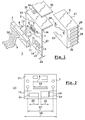
- FIG. 1 shows an optoelectronic device 1 according to the invention.
- the device 1 comprises a printed circuit 2, a connector 3, and a radiator 4.
- the printed circuit 2 includes an optical transceiver 5.
- the transmitter optical receiver 5 has optical contacts 6 for respectively send or receive optical signals.
- the transceiver 5 is a electro-optical conversion component
- the transceiver 5 is a matrix of diodes called VCSEL (Vertical Cavity Solid Emitting Laser; solid emission laser with vertical cavity), or a matrix of PIN photodiodes.
- the optical contacts 6 are diodes, to only emit a signal.
- the transmitter and or receiver 5 is a simple optical transmitter.
- the transceiver 5 can also be a zone of the circuit printed leaving flush with the ends of optical fibers, these fibers optics which can for example be included in the thickness of the circuit printed. Then the optical contacts 6 correspond to these ends of optical fiber.
- the printed circuit 2 also comprises two orifices 7, these orifices 7 preferably being arranged on either side of the transceiver 5.
- the orifices 7 then form a pair. They are precisely positioned opposite optical contacts 6.
- provision can be made for the printed circuit 2 has several orifices such as 7, and then in a preferred embodiment of this variant, it may include several pairs of holes 7.
- the orifices 7 are more particularly provided for receiving centering pins.
- centering pins 8 are presented on the optical connector 3 to be able to place this optical connector 3 of correctly on the printed circuit.
- the centering pins 8 are precisely positioned vis-à-vis the optical contacts (not shown) of connector 3. Indeed, the facing of connector 3 with the transceiver 5 requires very high precision being given the precision required for optical links in general.
- the connector 3 is for example connected to a cable 9 comprising optical fibers 10.
- the optical fibers 10 are for example arranged at the inside of connector 3 so that the ends (not shown) of these optical fibers 10 are flush at a front face 11 of connector 3. This front face 11 is intended to be placed next to the contact matrix 6.
- the flush ends of the optical fibers 10 are then to be put opposite the optical contacts 6.
- optical contacts 6 are spaced such that a spacing between these optical contacts is of the order of the spacing of those shown on connector 3.
- the centering pins 8 cooperate with the orifices 7 at a correct placement of connector 3 with printed circuit 2 so that ensure a correct optical path between these two elements.
- the transceiver 5 is more particularly arranged on a first element 13 of printed circuit 2.
- This first element 13 comprises for example other electronic devices 14 mounted on the surface of a side 15 of this element 13.
- the transceiver 5 is also presented on this face 15.
- a device 14 can be an amplifier, or a signal processing component.
- the first element 13 has tracks (not shown) for connecting the transmitter optical receiver 5 with these other devices 14.
- this first element 13 comprises, in a preferred embodiment, two transceivers such as 5.
- the printed circuit 2 can thus receive one or two connectors.
- the first element 13 comprises two pairs of orifices 7.
- the orifices of a pair are respectively arranged on either side of a transceiver 5 presented on this face 15.
- a complementary connector comprising two pairs centering pins such as 8 can be mounted on this printed circuit 2.
- the first element 13 is for example of very small size.
- a width 16 of this element 13 is of the order of 10 millimeters.
- the first element 13 has a square shape.
- a gap 17 between two orifices 7 of the same pair is on the order of 6.5 millimeters. Therefore, a width 18 of a transmitter receiver 5 is less than the distance 17.
- this width 18 is in the range of 2 to 2.5 millimeters.
- this face 15 has a amplifier 19, such as this amplifier 19 has for example a width of around 1.7 millimeters.
- the face 15 may also include a control circuit 20 with a width of around 2 millimeters.
- the first printed circuit element 13 2 comprises the face 15, and also a second face 23. This second face 23 is opposite the face 15, while being parallel thereto.
- the first element 13 is a plate 24 thin.
- the face 23 is applied against the radiator 4. In the example presented in FIG. 1, the face 23 is applied against a first face 25 of this radiator 4.
- this first face 25 also has orifices 26, so that when the first element 13 is applied against the first face 25, the orifices 7 are arranged opposite the orifices 26.
- the first face 25 has at least one pair of orifices 26 so as to be placed facing the pair of orifices such as 7.
- the centering pins 8 can also be inserted into orifice 26, and held there. So, the orifices 26 can participate in correct positioning of the connector 3 on the printed circuit 2.
- the radiator 4 is preferably made of a material to dissipate a large amount of heat. It is characterized by good heat exchange capacities.
- the radiator 4 stiffens the overall structure of this device 1.
- the radiator 4 is a module of parallelepiped shape then comprising a second face 27.
- This second face 27 is distinct of the first face 25.
- the second face 27 is secant with respect to the first face 25.
- the face 25 is perpendicular to the second face 27.
- the radiator 4 may have an openwork face 28.
- This face perforated 28 may include one or more cavities 29.
- the cavities 29 are hollowed inwards from the parallelepiped formed by the radiator 4.
- the cavities 29 also open on at least another face 30 of the radiator 4.
- the cavities 29 are separated from each other others by walls 31 of a certain thickness.
- the area total developed by such a radiator 4 is significantly increased by the play of these cavities 29 and walls 31. The increase in the contact surface between the external environment, for example air, and the radiator allows better heat dissipation.
- the printed circuit 2 also includes a second element 32 of printed circuit board.
- the second element 32 is connected to the first element 13 by through a portion of the flexible printed circuit 33.
- the printed circuit 2 comprises at least the following three portions: the first element 13, the second element 32 and the flexible portion 33.
- the printed circuit elements 13 and 32 can be placed in separate planes. Indeed, we can place the flexible circuit 33 so that it forms an elbow 33. In a preferred example, the elbow 33 forms an angle 34 of the order of 90 °.
- the first element 13 and the second element 32 consist of portions of rigid printed circuit, while the portion 33 is flexible.
- the portions 13, 32 and 33 are all flexible.
- the printed circuit 2 consists of a single piece, and the portions simply correspond to different orientations.
- the portions 13, 32 and 33 of the printed circuit 2 are applied to the periphery of the radiator 4.
- the second printed circuit element 32 therefore has a surface complementary to the first element 13 for receiving connectors, and or components, and / or other electronic devices to be connected with the device 1.
- the second printed circuit element 32 can receive the connection elements allowing the connection of the device 1 to an additional device 35, for example on a card mother.
- the connection between the second element 32 and the complementary device 35 is for example provided by a microbead system.
- the electrical and physical connection made by the microbead system is more particularly described in the documents US-A-6,024,584, and US-A-5,598,033.
- connection is then ensured by solder balls 36, the balls 36 then being arranged so as to form a table respecting a certain geometry to authorize a connection correct single additional device 35 can be connected with the second element 32.
- the balls 36 are micro-welded, and are commonly called “ball grid array”, according to English terminology, by the skilled person.
- the device 1 includes reinforcement plates 37.
- the reinforcement plates 37 make it possible to stiffen the printed circuit board.
- These reinforcing plates 37 are more particularly disposed at the orifices 7.
- these reinforcing strips 37 are generally arranged around a circumference of the circuit elements printed 2 to facilitate handling and prevent placement of the flexible printed circuit 33. Indeed, if the printed circuit is flexible, the area where the elbow should be made is uncertain but in the presence reinforcement plates 37, these fold zones are limited and thus ensures correct placement of the printed circuit 2 on the radiator 4. Indeed, there is a preferred position of the portion 13 relative to the first face 25, and of the second element 32 relative to the second face 27.
- These reinforcing plates can be of a calibrated thickness of so as to control the space between the surface of the optical components 6 and the end of the fibers 10.
Abstract
Description
La présente invention a pour objet un dispositif optoélectronique émetteur et ou récepteur. Elle trouve plus particulièrement son utilisation dans le domaine des connexions optiques à haut débit, notamment celles respectant des normes d'usage dans les télécommunications. Dans l'état de la technique, on connaít un dispositif de ce type comportant un circuit imprimé sur lequel est disposé un émetteur récepteur optique, pour émettre ou recevoir ces signaux optiques échangés avec un connecteur optique disposé en vis-à-vis de cet émetteur récepteur optique. De tels dispositifs dissipent beaucoup d'énergie, et sont généralement munis d'un radiateur pour assurer leur refroidissement. L'intérêt de l'invention est quelle présente un dispositif optoélectronique muni d'un radiateur, de telle sorte que le radiateur sert également de support mécanique au dispositif.The present invention relates to an optoelectronic device transmitter and or receiver. It finds more particularly its use in the field of high speed optical connections, especially those respecting standards of use in telecommunications. In the state of the technique, we know a device of this type comprising a circuit printed on which is placed an optical transceiver, to transmit or receive these optical signals exchanged with an optical connector arranged opposite this optical transceiver. Such devices dissipate a lot of energy, and are generally equipped with a radiator to keep them cool. The interest of the invention is what presents an optoelectronic device fitted with a radiator, so that the radiator also serves as a mechanical support for the device.
Dans l'état de la technique, on connaít une liaison optique parallèle, de l'enseignement du document IEEE 078035234 3/99 Electronic Competence and Technologic Conference. Cette liaison optique parallèle met en oeuvre un émetteur récepteur et un connecteur complémentaire relié à une fibre optique. A cet effet, elle comporte un circuit imprimé sur lequel est présenté un émetteur récepteur présentant des photodiodes alignées, le circuit imprimé étant conçu de manière à ce que le connecteur complémentaire puisse être monté à la surface de ce circuit imprimé et présenté en vis-à-vis de l'émetteur récepteur optique. Par exemple, le connecteur complémentaire présente des extrémités de fibres optiques reliées à ce connecteur avec un écartement de ses extrémités égal à l'écartement entre les photodiodes de l'émetteur récepteur.In the state of the art, there is known a parallel optical link, of teaching the document IEEE 078035234 3/99 Electronic Competence and Technologic Conference. This parallel optical link implements a transceiver and a complementary connector connected to an optical fiber. For this purpose, it includes a printed circuit on which is presented a transceiver with aligned photodiodes, the printed circuit being designed so that the connector can be mounted on the surface of this printed circuit and presented opposite the optical transceiver. For example, the complementary connector has fiber optic ends connected to this connector with a spacing of its ends equal to the spacing between the photodiodes of the transceiver.
De plus, pour assurer le montage correct du connecteur complémentaire sur le circuit imprimé, le circuit imprimé comporte deux orifices et le connecteur comporte en correspondance deux pions de guidage. La position des extrémités des fibres optiques est précisément définie par rapport aux pions de guidage, de même la position des photodiodes est précisément définie par rapport aux orifices du circuit imprimé. Ainsi on aboutit, lors du montage du connecteur complémentaire à la surface du circuit imprimé, à une connexion optique de précision entre les fibres optiques et l'émetteur récepteur optique. In addition, to ensure the correct mounting of the connector on the printed circuit, the printed circuit has two holes and the connector has corresponding two pins of guide. The position of the ends of the optical fibers is precisely defined with respect to the guide pins, the position of the photodiodes is precisely defined in relation to the orifices of the circuit printed. Thus, when the complementary connector is assembled, the surface of the printed circuit, to a precision optical connection between the fiber optics and the optical transceiver.
Cette liaison optique parallèle comporte de plus une embase métallique pour pouvoir dissiper la chaleur émise par l'ensemble des composants électroniques portés par le circuit imprimé, notamment celle émise par les photodiodes. L'embase métallique est une plaque appliquée contre une face du circuit imprimé, préférentiellement en regard de l'émetteur récepteur. Dans un exemple préféré, cette embase métallique comporte également des orifices d'alignement. Ainsi, l'embase métallique peut également recevoir les pions de centrage du connecteur complémentaire.This parallel optical link also includes a base metallic to be able to dissipate the heat emitted by all of the electronic components carried by the printed circuit, in particular that emitted by photodiodes. The metal base is an applied plate against one side of the printed circuit, preferably facing the transmitter receiver. In a preferred example, this metal base comprises also alignment holes. Thus, the metal base can also receive the centering pins of the complementary connector.
Dans cet exemple, le circuit imprimé est flexible, et il comporte plusieurs portions permettant une connexion avec différents dispositifs. Par exemple, une première portion est destinée à être connectée avec le connecteur complémentaire. Dans ce cas, l'embase métallique est appliquée contre cette seule première portion. D'autre part, une deuxième portion du circuit imprimé est prévue pour être reliée, par un système de billes de soudure, à un autre dispositif, telle qu'une carte mère par exemple. Généralement un tel dispositif comporte une troisième portion de circuit imprimé, laquelle troisième portion est prévue plus particulièrement pour recevoir des composants passifs.In this example, the printed circuit is flexible, and it includes several portions allowing connection with different devices. Through example, a first portion is intended to be connected with the additional connector. In this case, the metal base is applied against that one first serving. On the other hand, a second portion of the printed circuit is intended to be connected, by a system of balls of soldering, to another device, such as a motherboard for example. Generally such a device comprises a third portion of circuit printed, which third portion is intended more particularly for receive passive components.
Ce dispositif optoélectronique de l'état de la technique pose un problème. En effet, un tel dispositif optoélectronique dégage beaucoup de chaleur. Or l'embase métallique prévue pour servir de radiateur est généralement d'une taille inférieure à celle du circuit imprimé. En effet, le circuit imprimé étant flexible, et les différentes portions de ce circuit n'étant pas nécessairement alignées, l'embase métallique, qui est une plaque rigide, ne peut pas suivre les différentes portions du circuit imprimé. Donc, en général l'intérêt de cette embase métallique est limité au rôle de radiateur, dans la zone très restreinte où celui-ci est disposé.This optoelectronic device of the state of the art poses a problem. Indeed, such an optoelectronic device releases a lot of heat. However, the metal base intended to serve as a radiator is generally of a size smaller than that of the printed circuit. Indeed, the printed circuit being flexible, and the different portions of this circuit being not necessarily aligned, the metal base, which is a rigid plate, cannot follow the different portions of the printed circuit. So in general the interest of this metal base is limited to the role of radiator, in the very restricted area where it is located.
De plus, le circuit imprimé flexible risque de subir des frottements au niveau du pourtour de l'embase métallique. En effet, cette embase métallique étant locale, elle comporte des bordures présentées de manière saillante pour le circuit imprimé flexible. Par exemple, si le circuit imprimé flexible est courbé de telle sorte qu'il se replie sur l'embase métallique, alors, les bordures saillantes risquent de le couper localement. Par ailleurs, l'embase métallique étant de très fine épaisseur, cette courbure du circuit imprimé flexible peut aboutir à la formation d'un coude très serré autour de cette embase métallique et donc risquer de détériorer des pistes conductrices prévues à cet endroit sur le circuit imprimé flexible.In addition, the flexible printed circuit may be subject to friction at level around the metal base. Indeed, this metal base being local, it has raised edges for the flexible printed circuit. For example, if the flexible printed circuit is curved so that it folds over the metal base, then the protruding edges may cut it locally. In addition, the base metal being very thin, this curvature of the printed circuit flexible can result in the formation of a very tight bend around this metal base and therefore risk damaging conductive tracks provided at this point on the flexible printed circuit.
La présente invention a pour objet de résoudre le problème posé par le dispositif optoélectronique de l'état de la technique. En effet, le dispositif optoélectronique émetteur et ou récepteur de l'invention prévoit plus particulièrement un dispositif comportant un circuit imprimé tel que ce circuit imprimé est appliqué contre un radiateur, ce radiateur ayant une forme telle qu'il comporte plusieurs faces distinctes. Le circuit imprimé comporte au moins un récepteur et ou émetteur optique, et peut recevoir au moins un connecteur optique complémentaire, de telle sorte que des pions de centrage de ce connecteur peuvent être insérés dans des orifices du circuit. Dans cette position de connexion, des contacts optiques du connecteur complémentaire sont disposés en vis-à-vis des contacts de l'émetteur récepteur optique du circuit.The object of the present invention is to solve the problem posed by the optoelectronic device of the state of the art. Indeed, the device optoelectronic transmitter and or receiver of the invention provides more particularly a device comprising a printed circuit such as this circuit printed is applied against a radiator, this radiator having such a shape that it has several distinct faces. The printed circuit includes at at least one optical receiver and or transmitter, and can receive at least one additional optical connector, so that centering pins of this connector can be inserted into holes in the circuit. In this connection position, optical contacts of the connector are arranged opposite the transmitter contacts optical circuit receiver.
Le circuit imprimé de l'invention est particulier car il comporte une première portion appliquée contre une première face du radiateur, et une deuxième portion de ce même circuit imprimé appliquée contre une deuxième face de ce même radiateur. La particularité de l'invention réside dans le fait que les deux faces sur lesquelles le circuit imprimé est appliqué sont distinctes, ou par exemple contiguës. Le circuit imprimé comporte de plus une portion flexible, telle que cette portion flexible assure une liaison entre la première portion et la deuxième portion. La portion flexible permet notamment de placer la première et la deuxième portion sur des plans différents. Par conséquent, le radiateur joue un rôle de support physique pour au moins ces deux portions de circuit imprimé, et les protège des détériorations.The printed circuit of the invention is special because it includes a first portion applied against a first face of the radiator, and a second portion of this same printed circuit applied against a second side of the same radiator. The peculiarity of the invention lies in that the two faces on which the printed circuit is applied are distinct, or for example contiguous. The printed circuit includes plus a flexible portion, such that this flexible portion provides a connection between the first portion and the second portion. The flexible portion allows including placing the first and second portions on plans different. Consequently, the radiator plays a role of physical support for at least these two portions of printed circuit, and protects them from damage.
L'invention concerne donc un dispositif optoélectronique comportant un premier élément de circuit imprimé, sur lequel est monté un émetteur et ou récepteur optique, ce premier élément de circuit imprimé comportant au moins deux orifices pour recevoir des pions de centrage d'un connecteur optique pouvant être montés en vis-à-vis de l'émetteur et ou récepteur optique, ce dispositif comportant en outre un radiateur, étant caractérisé en ce le premier élément de circuit imprimé est appliqué contre une première face du radiateur, et en ce qu'une portion de circuit imprimé flexible relie le premier élément de circuit imprimé à un deuxième élément de circuit imprimé, ce deuxième élément de circuit imprimé étant appliqué contre une deuxième face du radiateur, cette deuxième face étant distincte de la première face.The invention therefore relates to an optoelectronic device comprising a first printed circuit element, on which is mounted a transmitter and or optical receiver, this first printed circuit element comprising at at least two holes to receive centering pins from a connector optic which can be mounted opposite the transmitter and / or receiver optical, this device further comprising a radiator, being characterized in that the first printed circuit element is applied against a first face of the radiator, and in that a flexible printed circuit portion connects the first circuit element to a second circuit element printed, this second printed circuit element being applied against a second face of the radiator, this second face being distinct from the first side.
L'invention sera mieux comprise à la lecture de la description qui suit et à l'examen des figures qui l'accompagnent. Celles-ci ne sont présentées qu'à titre indicatif et nullement limitatif de l'invention. Les figures montrent :
- Figure 1: Une vue éclatée en perpective d'un dispositif optoélectronique selon l'invention ;
- Figure 2 : Une vue d'une face d'un élément de circuit imprimé d'un dispositif optoélectronique selon l'invention.
- Figure 1: An exploded perspective view of an optoelectronic device according to the invention;
- Figure 2: A front view of a printed circuit element of an optoelectronic device according to the invention.
La Figure 1 présente un dispositif optoélectronique 1 selon l'invention.
Le dispositif 1 comporte un circuit imprimé 2, un connecteur 3, et un radiateur
4. Le circuit imprimé 2 comporte un émetteur récepteur optique 5. L'émetteur
récepteur optique 5 comporte des contacts optiques 6 pour respectivement
envoyer ou recevoir des signaux optiques. L'émetteur récepteur 5 est un
composant de conversion électro-optique Par exemple, l'émetteur récepteur
5 est une matrice de diodes dites VCSEL (Vertical Cavity Solid Emitting
Laser ; laser d'émission solide à cavité verticale), ou une matrice de
photodiodes PIN. Dans une variante, les contacts optiques 6 sont des
diodes, pour seulement émettre un signal. Dans cette variante, l'émetteur et
ou récepteur 5 est un simple émetteur optique.Figure 1 shows an
L'émetteur récepteur 5 peut également être une zone du circuit
imprimé laissant affleurer des extrémités de fibres optiques, ces fibres
optiques pouvant être par exemple incluses dans l'épaisseur du circuit
imprimé. Alors les contacts optiques 6 correspondent à ces extrémités de
fibres optiques.The
Le circuit imprimé 2 comporte par ailleurs deux orifices 7, ces orifices
7 étant préférentiellement disposés de part et d'autre de l'émetteur récepteur
5. Les orifices 7 forment alors une paire. Ils sont précisément positionnés vis-à-vis
des contacts optiques 6. Dans une variante, on peut prévoir que le
circuit imprimé 2 comporte plusieurs orifices tels que 7, et alors dans un
mode de réalisation préféré de cette variante, il peut comporter plusieurs
paires d'orifices 7.The printed
Les orifices 7 sont plus particulièrement prévus pour recevoir des
pions de centrage. A cet effet, des pions de centrage 8 sont présentés sur le
connecteur optique 3 pour pouvoir placer ce connecteur optique 3 de
manière correcte sur le circuit imprimé. De même, les pions de centrage 8
sont précisément positionnés vis-à-vis des contacts optiques (non
représentés) du connecteur 3. En effet, la mise en vis-à-vis du connecteur 3
avec l'émetteur récepteur 5 nécessite une très grande précision étant
donnée la précision requise pour les liaisons optiques en général.The
Le connecteur 3 est par exemple relié à un câble 9 comportant des
fibres optiques 10. Les fibres optiques 10 sont par exemple agencées à
l'intérieur du connecteur 3 de manière à ce que des extrémités (non
représentées) de ces fibres optiques 10 soient affleurantes au niveau d'une
face avant 11 du connecteur 3. Cette face avant 11 est destinée à être
placée en regard de la matrice de contacts 6.The
Les extrémités affleurantes des fibres optiques 10 sont alors à mettre
en vis-à-vis des contacts optiques 6.The flush ends of the
Par ailleurs, les contacts optiques 6 sont espacés de telle sorte qu'un
espacement entre ces contacts optiques est de l'ordre de l'espacement de
ceux présentés sur le connecteur 3. Quand le connecteur 3 est monté sur le
circuit imprimé 2, les pions de centrage 8 coopèrent avec les orifices 7 à un
placement correct du connecteur 3 avec le circuit imprimé 2 de manière à
assurer un chemin optique correct entre ces deux éléments.Furthermore, the optical contacts 6 are spaced such that a
spacing between these optical contacts is of the order of the spacing of
those shown on
L'émetteur récepteur 5 est plus particulièrement disposé sur un
premier élément 13 de circuit imprimé 2. Ce premier élément 13 comporte
par exemple d'autres dispositifs électroniques 14 montés à la surface d'une
face 15 de cet élément 13. L'émetteur récepteur 5 est également présenté
sur cette face 15. Par exemple, un dispositif 14 peut être un amplificateur, ou
un composant de traitement de signal. Dans ce cas, le premier élément 13
comporte des pistes (non représentées) permettant de relier l'émetteur
récepteur optique 5 avec ces autres dispositifs 14. Comme présenté figure 2,
ce premier élément 13 comporte, dans un exemple préféré de réalisation,
deux émetteurs récepteurs tels que 5. Le circuit imprimé 2 peut ainsi recevoir
un ou deux connecteurs. Dans cet exemple, le premier élément 13 comporte
deux paires d'orifices 7. Les orifices d'une paire sont respectivement
disposés de part et d'autre d'un émetteur récepteur 5 présenté sur cette face
15. Dans un tel cas, un connecteur complémentaire comportant deux paires
de pions de centrage tels que 8 peut être monté sur ce circuit imprimé 2. The
Le premier élément 13 est par exemple de taille très réduite. Par
exemple une largeur 16 de cet élément 13 est de l'ordre de 10 millimètres.
Dans un exemple préféré, le premier élément 13 a une forme carrée. Dans
cet exemple préféré, un écart 17 entre deux orifices 7 d'une même paire est
de l'ordre de 6,5 millimètres. Par conséquent, une largeur 18 d'un émetteur
récepteur 5 est inférieure à l'écart 17. Par exemple cette largeur 18 est de
l'ordre de 2 à 2,5 millimètres. De plus, cette face 15 présente un
amplificateur 19, tel que cet amplificateur 19 a par exemple une largeur de
l'ordre de 1,7 millimètres. De plus, la face 15 peut comporter également un
circuit de pilotage 20 d'une largeur de l'ordre de 2 millimètres environ.The
Le premier élément 13 de circuit imprimé 2 comporte la face 15, et
également une deuxième face 23. Cette deuxième face 23 est opposée à la
face 15, tout en lui étant parallèle. Le premier élément 13 est une plaque
d'une épaisseur 24 faible. La face 23 est appliquée contre le radiateur 4.
Dans l'exemple présenté figure 1, la face 23 est appliquée contre une
première face 25 de ce radiateur 4.The first printed
Dans un mode de réalisation préféré, cette première face 25
comporte également des orifices 26, de telle sorte que, lorsque le premier
élément 13 est appliqué contre la première face 25, les orifices 7 soient
disposés en vis-à-vis des orifices 26. A cet effet, la première face 25
comporte au moins une paire d'orifices 26 pour être placé en vis-à-vis de la
paire d'orifices tel que 7. Ainsi, lorsque le connecteur 3 est monté sur la face
15 du premier élément 13 de circuit imprimé 2, les pions de centrage 8
peuvent également être insérés dans l'orifice 26, et y être maintenus. Ainsi,
les orifices 26 peuvent participer à un positionnement correct du connecteur
3 sur le circuit imprimé 2.In a preferred embodiment, this
Le radiateur 4 est préférentiellement réalisé dans un matériau permettant de dissiper une grande quantité de chaleur. Il est caractérisé par de bonnes capacités d'échange thermique.The radiator 4 is preferably made of a material to dissipate a large amount of heat. It is characterized by good heat exchange capacities.
Le radiateur 4 permet de rigidifier la structure globale de ce dispositif
1. Par exemple, le radiateur 4 est un module de forme parallelépipédique
comportant alors une deuxième face 27. Cette deuxième face 27 est distincte
de la première face 25. Dans l'exemple présenté figure 1, la deuxième face
27 est sécante par rapport à la première face 25. Dans un mode de
réalisation préféré, la face 25 est perpendiculaire à la deuxième face 27. Par
exemple, le radiateur 4 peut comporter une face ajourée 28. Cette face
ajourée 28 peut comporter une ou plusieurs cavités 29. Les cavités 29 sont
creusées vers l'intérieur du parallélépipède formé par le radiateur 4. Dans
l'exemple présenté figure 1, les cavités 29 ouvrent également sur au moins
une autre face 30 du radiateur 4. Les cavités 29 sont séparées les unes des
autres par des murs 31 d'une certaine épaisseur. Par ailleurs, la superficie
totale développée par un tel radiateur 4 est nettement augmentée par le jeu
de ces cavités 29 et murs 31. L'augmentation de la surface de contact entre
l'environnement extérieur, par exemple l'air, et le radiateur permet une
meilleure dissipation de la chaleur.The radiator 4 stiffens the overall structure of this
Le circuit imprimé 2 comporte également un deuxième élément 32 de
circuit imprimé. Le deuxième élément 32 est relié au premier élément 13 par
l'intermédiaire d'une portion du circuit imprimé flexible 33. Dans cet exemple,
le circuit imprimé 2 comporte au moins les trois portions suivantes : le
premier élément 13, le deuxième élément 32 et la portion flexible 33. Par le
jeu de la portion flexible 33, les éléments de circuit imprimé 13 et 32 peuvent
être placés dans des plans distincts. En effet, on peut placer le circuit flexible
33 de telle sorte qu'il forme un coude 33. Dans un exemple préféré, le coude
33 forme un angle 34 de l'ordre de 90°.The printed
Dans l'exemple présenté figure 1, le premier élément 13 et le
deuxième élément 32 sont constitués de portions de circuit imprimé rigide,
alors que la portion 33 est flexible. Dans une variante, on peut prévoir que
les portions 13, 32 et 33 sont toutes flexibles. Dans ce cas, le circuit imprimé
2 est constitué d'un unique tenant, et les portions correspondent simplement
à des orientations différentes. Les portions 13, 32 et 33 du circuit imprimé 2
sont appliquées à la périphérie du radiateur 4.In the example presented in FIG. 1, the
Le deuxième élément de circuit imprimé 32 présente donc une surface
complémentaire du premier élément 13 pour recevoir des connecteurs, et ou
des composants, et ou encore d'autres dispositifs électroniques à connecter
avec le dispositif 1. Par exemple, le deuxième élément de circuit imprimé 32
peut recevoir les éléments de connexion permettant le raccordement du
dispositif 1 à un dispositif complémentaire 35, par exemple sur une carte
mère. Dans une mode de réalisation préféré, la connexion entre le deuxième
élément 32 et le dispositif complémentaire 35 est par exemple assurée par
un système de microbilles. La liaison électrique et physique réalisée par le
système de microbille est plus particulièrement décrite dans les documents
US-A-6,024,584, et US-A-5,598,033. La liaison est alors assurée par des
billes de soudure 36, les billes 36 étant alors disposées de manière à former
un tableau respectant une certaine géométrie pour autoriser une connexion
correcte unique du dispositif complémentaire 35 pouvant être connectés
avec le deuxième élément 32. Les billes 36 sont micro-soudées, et sont
couramment appelées "ball grid array", selon la terminologie anglo saxonne,
par l'homme du métier.The second printed
Dans le mode de réalisation où le circuit imprimé est entièrement
flexible et dans lequel le premier élément 13 et le deuxième élément 32 sont
également flexibles, comme présenté figure 2, le dispositif 1 comporte des
plaques de renfort 37. Les plaques de renfort 37 permettent de rigidifier le
circuit imprimé. Ces plaques de renfort 37 sont plus particulièrement
disposées au niveau des orifices 7. Par ailleurs, ces bandes de renfort 37
sont généralement disposées sur un pourtour des éléments de circuit
imprimé 2 pour faciliter leur manipulation et empêcher les placements
incorrects du circuit imprimé flexible 33. En effet, si le circuit imprimé est
flexible, la zone où le coude doit être réalisé est incertaine mais en présence
des plaques de renfort 37, ces zones de pliures sont limitées et ainsi on
assure un placement correct du circuit imprimé 2 sur le radiateur 4. En effet,
il existe une position préférée de la portion 13 relativement à la première face
25, et du deuxième élément 32 relativement à la deuxième face 27.In the embodiment where the printed circuit is entirely
flexible and in which the
Ces plaques de renfort peuvent être d'une épaisseur calibrée de
manière à contrôler l'espace entre la surface des composants optiques 6 et
l'extrémité des fibres 10.These reinforcing plates can be of a calibrated thickness of
so as to control the space between the surface of the optical components 6 and
the end of the
Claims (10)
Applications Claiming Priority (2)
| Application Number | Priority Date | Filing Date | Title |
|---|---|---|---|
| FR0013767A FR2816111B1 (en) | 2000-10-26 | 2000-10-26 | OPTOELECTRONIC TRANSCEIVER DEVICE |
| FR0013767 | 2000-10-26 |
Publications (2)
| Publication Number | Publication Date |
|---|---|
| EP1217404A1 true EP1217404A1 (en) | 2002-06-26 |
| EP1217404B1 EP1217404B1 (en) | 2003-07-23 |
Family
ID=8855780
Family Applications (1)
| Application Number | Title | Priority Date | Filing Date |
|---|---|---|---|
| EP01000562A Expired - Lifetime EP1217404B1 (en) | 2000-10-26 | 2001-10-22 | Opto-electronic module with a transmitter/receiver mounted onto a printed circuit board in contact with a cooling radiator |
Country Status (5)
| Country | Link |
|---|---|
| US (1) | US6767142B2 (en) |
| EP (1) | EP1217404B1 (en) |
| AT (1) | ATE245823T1 (en) |
| DE (1) | DE60100498T2 (en) |
| FR (1) | FR2816111B1 (en) |
Cited By (1)
| Publication number | Priority date | Publication date | Assignee | Title |
|---|---|---|---|---|
| CN110097994A (en) * | 2019-05-13 | 2019-08-06 | 浙江大学 | A kind of system and method for repeating to capture microballoon based on pulse laser |
Families Citing this family (10)
| Publication number | Priority date | Publication date | Assignee | Title |
|---|---|---|---|---|
| US7056032B2 (en) * | 2001-09-17 | 2006-06-06 | Stratos International, Inc. | Transceiver assembly for use in fiber optics communications |
| US6705769B2 (en) * | 2001-09-20 | 2004-03-16 | International Business Machines Corporation | Packaging architecture for a multiple array transceiver using a flexible cable |
| US7070341B2 (en) * | 2002-10-02 | 2006-07-04 | Emcore Corporation | High-density fiber-optic module with multi-fold flexible circuit |
| US7128472B2 (en) * | 2003-07-31 | 2006-10-31 | International Business Machines Corporation | Method and apparatus for providing optoelectronic communication with an electronic device |
| KR20070083962A (en) | 2004-11-12 | 2007-08-24 | 도레이 가부시끼가이샤 | White film and backlight using same |
| CN102385125A (en) * | 2011-10-28 | 2012-03-21 | 江苏奥雷光电有限公司 | Multi-channel small form-factor transceiver and assembly method |
| US9134490B2 (en) * | 2012-12-06 | 2015-09-15 | Laxense Inc. | Passive alignment multichannel parallel optical system |
| US10025049B2 (en) * | 2014-07-23 | 2018-07-17 | Fci Usa Llc | Optoelectrical connector module |
| US10830972B2 (en) * | 2016-02-01 | 2020-11-10 | Sony Corporation | Optical connector, electronic apparatus and optical interconnection system |
| JP7426839B2 (en) | 2020-01-28 | 2024-02-02 | 古河電気工業株式会社 | Optical module manufacturing method |
Citations (7)
| Publication number | Priority date | Publication date | Assignee | Title |
|---|---|---|---|---|
| US3766439A (en) * | 1972-01-12 | 1973-10-16 | Gen Electric | Electronic module using flexible printed circuit board with heat sink means |
| US4763225A (en) * | 1985-08-30 | 1988-08-09 | Siemens Aktiengesellschaft | Heat dissipating housing for an electronic component |
| EP0314651A2 (en) * | 1987-10-30 | 1989-05-03 | International Business Machines Corporation | Electro-optical transducer assembly |
| US5011256A (en) * | 1988-10-28 | 1991-04-30 | E. I. Du Pont De Nemours And Company | Package for an opto-electronic component |
| US5168537A (en) * | 1991-06-28 | 1992-12-01 | Digital Equipment Corporation | Method and apparatus for coupling light between an optoelectronic device and a waveguide |
| US5241614A (en) * | 1991-04-29 | 1993-08-31 | International Business Machines Corporation | Apparatus and a method for an optical fiber interface |
| US5396573A (en) * | 1993-08-03 | 1995-03-07 | International Business Machines Corporation | Pluggable connectors for connecting large numbers of electrical and/or optical cables to a module through a seal |
Family Cites Families (5)
| Publication number | Priority date | Publication date | Assignee | Title |
|---|---|---|---|---|
| US5604831A (en) | 1992-11-16 | 1997-02-18 | International Business Machines Corporation | Optical module with fluxless laser reflow soldered joints |
| US5598033A (en) | 1995-10-16 | 1997-01-28 | Advanced Micro Devices, Inc. | Micro BGA stacking scheme |
| US6024584A (en) | 1996-10-10 | 2000-02-15 | Berg Technology, Inc. | High density connector |
| US5768456A (en) * | 1996-11-22 | 1998-06-16 | Motorola, Inc. | Optoelectronic package including photonic device mounted in flexible substrate |
| US6318909B1 (en) * | 1999-02-11 | 2001-11-20 | Agilent Technologies, Inc. | Integrated packaging system for optical communications devices that provides automatic alignment with optical fibers |
-
2000
- 2000-10-26 FR FR0013767A patent/FR2816111B1/en not_active Expired - Fee Related
-
2001
- 2001-10-22 AT AT01000562T patent/ATE245823T1/en not_active IP Right Cessation
- 2001-10-22 EP EP01000562A patent/EP1217404B1/en not_active Expired - Lifetime
- 2001-10-22 DE DE60100498T patent/DE60100498T2/en not_active Expired - Fee Related
- 2001-10-26 US US10/046,327 patent/US6767142B2/en not_active Expired - Fee Related
Patent Citations (7)
| Publication number | Priority date | Publication date | Assignee | Title |
|---|---|---|---|---|
| US3766439A (en) * | 1972-01-12 | 1973-10-16 | Gen Electric | Electronic module using flexible printed circuit board with heat sink means |
| US4763225A (en) * | 1985-08-30 | 1988-08-09 | Siemens Aktiengesellschaft | Heat dissipating housing for an electronic component |
| EP0314651A2 (en) * | 1987-10-30 | 1989-05-03 | International Business Machines Corporation | Electro-optical transducer assembly |
| US5011256A (en) * | 1988-10-28 | 1991-04-30 | E. I. Du Pont De Nemours And Company | Package for an opto-electronic component |
| US5241614A (en) * | 1991-04-29 | 1993-08-31 | International Business Machines Corporation | Apparatus and a method for an optical fiber interface |
| US5168537A (en) * | 1991-06-28 | 1992-12-01 | Digital Equipment Corporation | Method and apparatus for coupling light between an optoelectronic device and a waveguide |
| US5396573A (en) * | 1993-08-03 | 1995-03-07 | International Business Machines Corporation | Pluggable connectors for connecting large numbers of electrical and/or optical cables to a module through a seal |
Cited By (2)
| Publication number | Priority date | Publication date | Assignee | Title |
|---|---|---|---|---|
| CN110097994A (en) * | 2019-05-13 | 2019-08-06 | 浙江大学 | A kind of system and method for repeating to capture microballoon based on pulse laser |
| CN110097994B (en) * | 2019-05-13 | 2020-08-14 | 浙江大学 | System and method for repeatedly capturing microspheres based on pulse laser |
Also Published As
| Publication number | Publication date |
|---|---|
| EP1217404B1 (en) | 2003-07-23 |
| US20020146218A1 (en) | 2002-10-10 |
| ATE245823T1 (en) | 2003-08-15 |
| DE60100498D1 (en) | 2003-08-28 |
| FR2816111A1 (en) | 2002-05-03 |
| US6767142B2 (en) | 2004-07-27 |
| FR2816111B1 (en) | 2003-01-03 |
| DE60100498T2 (en) | 2004-06-09 |
Similar Documents
| Publication | Publication Date | Title |
|---|---|---|
| JP5184708B1 (en) | Optical module | |
| JP5358537B2 (en) | Cage having heat sink device fixed by floating mechanism capable of maintaining continuous connection between heat sink device and parallel optical communication device | |
| US6739766B2 (en) | Lens array for use in parallel optics modules for fiber optics communications | |
| JP4479875B2 (en) | Optical subassembly | |
| US6729776B2 (en) | Transparent substrate and hinged optical assembly | |
| JP4477677B2 (en) | Optical module and manufacturing method thereof | |
| US7703991B2 (en) | Flip-chip mountable optical connector for chip-to-chip optical interconnectability | |
| EP1217404B1 (en) | Opto-electronic module with a transmitter/receiver mounted onto a printed circuit board in contact with a cooling radiator | |
| US20060133820A1 (en) | Transponder assembly for use with parallel optics modules in fiber optic communications systems | |
| US10050718B2 (en) | Optical communication module | |
| US9176288B2 (en) | Optical plug connector having an optical body with a lens on a reflective surface | |
| JP2008304903A (en) | Optical assembly and method of forming the same | |
| WO2003062891A1 (en) | Passive self-alignment technique for array laser transmitters andreceivers for fiber optic applications | |
| TW201426074A (en) | Optical communication module | |
| US20020154362A1 (en) | Optical link module | |
| US20140321819A1 (en) | Optical assembly | |
| FR2816066A1 (en) | ELECTRO-OPTICAL CONNECTION MODULE | |
| FR2875646A1 (en) | ELECTRICAL AND OPTICAL CONTACTING CONNECTOR PLUG | |
| TW201441703A (en) | Optical transmitting connector | |
| US9052485B2 (en) | Optical interconnect assembly | |
| US10007071B2 (en) | Optical bodies having a total internal reflection surface and a short optical path length | |
| WO2021200559A1 (en) | Photoelectric conversion module plug and optical cable | |
| US11112574B1 (en) | Optoelectronic system with a wedge-shaped adapter | |
| US20230023827A1 (en) | Fiber optic connector | |
| US20010033720A1 (en) | System and method for aligning optical components |
Legal Events
| Date | Code | Title | Description |
|---|---|---|---|
| PUAI | Public reference made under article 153(3) epc to a published international application that has entered the european phase |
Free format text: ORIGINAL CODE: 0009012 |
|
| AK | Designated contracting states |
Kind code of ref document: A1 Designated state(s): AT BE CH CY DE DK ES FI FR GB GR IE IT LI LU MC NL PT SE TR |
|
| AX | Request for extension of the european patent |
Free format text: AL;LT;LV;MK;RO;SI |
|
| 17P | Request for examination filed |
Effective date: 20021028 |
|
| GRAH | Despatch of communication of intention to grant a patent |
Free format text: ORIGINAL CODE: EPIDOS IGRA |
|
| RTI1 | Title (correction) |
Free format text: OPTO-ELECTRONIC MODULE WITH A TRANSMITTER/RECEIVER MOUNTED ONTO A PRINTED CIRCUIT BOARD IN CONTACT WITH A COOLING RADIATO |
|
| AKX | Designation fees paid |
Designated state(s): AT BE CH CY DE DK ES FI FR GB GR IE IT LI LU MC NL PT SE TR |
|
| GRAH | Despatch of communication of intention to grant a patent |
Free format text: ORIGINAL CODE: EPIDOS IGRA |
|
| GRAA | (expected) grant |
Free format text: ORIGINAL CODE: 0009210 |
|
| AK | Designated contracting states |
Designated state(s): AT BE CH CY DE DK ES FI FR GB GR IE IT LI LU MC NL PT SE TR |
|
| PG25 | Lapsed in a contracting state [announced via postgrant information from national office to epo] |
Ref country code: IT Free format text: LAPSE BECAUSE OF FAILURE TO SUBMIT A TRANSLATION OF THE DESCRIPTION OR TO PAY THE FEE WITHIN THE PRESCRIBED TIME-LIMIT;WARNING: LAPSES OF ITALIAN PATENTS WITH EFFECTIVE DATE BEFORE 2007 MAY HAVE OCCURRED AT ANY TIME BEFORE 2007. THE CORRECT EFFECTIVE DATE MAY BE DIFFERENT FROM THE ONE RECORDED. Effective date: 20030723 Ref country code: IE Free format text: LAPSE BECAUSE OF FAILURE TO SUBMIT A TRANSLATION OF THE DESCRIPTION OR TO PAY THE FEE WITHIN THE PRESCRIBED TIME-LIMIT Effective date: 20030723 Ref country code: NL Free format text: LAPSE BECAUSE OF FAILURE TO SUBMIT A TRANSLATION OF THE DESCRIPTION OR TO PAY THE FEE WITHIN THE PRESCRIBED TIME-LIMIT Effective date: 20030723 Ref country code: FI Free format text: LAPSE BECAUSE OF FAILURE TO SUBMIT A TRANSLATION OF THE DESCRIPTION OR TO PAY THE FEE WITHIN THE PRESCRIBED TIME-LIMIT Effective date: 20030723 Ref country code: ES Free format text: LAPSE BECAUSE OF FAILURE TO SUBMIT A TRANSLATION OF THE DESCRIPTION OR TO PAY THE FEE WITHIN THE PRESCRIBED TIME-LIMIT Effective date: 20030723 Ref country code: AT Free format text: LAPSE BECAUSE OF FAILURE TO SUBMIT A TRANSLATION OF THE DESCRIPTION OR TO PAY THE FEE WITHIN THE PRESCRIBED TIME-LIMIT Effective date: 20030723 Ref country code: TR Free format text: LAPSE BECAUSE OF FAILURE TO SUBMIT A TRANSLATION OF THE DESCRIPTION OR TO PAY THE FEE WITHIN THE PRESCRIBED TIME-LIMIT Effective date: 20030723 |
|
| REG | Reference to a national code |
Ref country code: GB Ref legal event code: FG4D Free format text: NOT ENGLISH |
|
| REG | Reference to a national code |
Ref country code: CH Ref legal event code: EP |
|
| REG | Reference to a national code |
Ref country code: IE Ref legal event code: FG4D Free format text: FRENCH |
|
| REF | Corresponds to: |
Ref document number: 60100498 Country of ref document: DE Date of ref document: 20030828 Kind code of ref document: P |
|
| PG25 | Lapsed in a contracting state [announced via postgrant information from national office to epo] |
Ref country code: CY Free format text: LAPSE BECAUSE OF FAILURE TO SUBMIT A TRANSLATION OF THE DESCRIPTION OR TO PAY THE FEE WITHIN THE PRESCRIBED TIME-LIMIT Effective date: 20031022 Ref country code: LU Free format text: LAPSE BECAUSE OF NON-PAYMENT OF DUE FEES Effective date: 20031022 |
|
| PG25 | Lapsed in a contracting state [announced via postgrant information from national office to epo] |
Ref country code: GR Free format text: LAPSE BECAUSE OF FAILURE TO SUBMIT A TRANSLATION OF THE DESCRIPTION OR TO PAY THE FEE WITHIN THE PRESCRIBED TIME-LIMIT Effective date: 20031023 Ref country code: SE Free format text: LAPSE BECAUSE OF FAILURE TO SUBMIT A TRANSLATION OF THE DESCRIPTION OR TO PAY THE FEE WITHIN THE PRESCRIBED TIME-LIMIT Effective date: 20031023 Ref country code: DK Free format text: LAPSE BECAUSE OF FAILURE TO SUBMIT A TRANSLATION OF THE DESCRIPTION OR TO PAY THE FEE WITHIN THE PRESCRIBED TIME-LIMIT Effective date: 20031023 |
|
| PG25 | Lapsed in a contracting state [announced via postgrant information from national office to epo] |
Ref country code: MC Free format text: LAPSE BECAUSE OF NON-PAYMENT OF DUE FEES Effective date: 20031031 Ref country code: BE Free format text: LAPSE BECAUSE OF NON-PAYMENT OF DUE FEES Effective date: 20031031 |
|
| NLV1 | Nl: lapsed or annulled due to failure to fulfill the requirements of art. 29p and 29m of the patents act | ||
| GBT | Gb: translation of ep patent filed (gb section 77(6)(a)/1977) |
Effective date: 20031112 |
|
| PG25 | Lapsed in a contracting state [announced via postgrant information from national office to epo] |
Ref country code: PT Free format text: LAPSE BECAUSE OF FAILURE TO SUBMIT A TRANSLATION OF THE DESCRIPTION OR TO PAY THE FEE WITHIN THE PRESCRIBED TIME-LIMIT Effective date: 20031223 |
|
| REG | Reference to a national code |
Ref country code: IE Ref legal event code: FD4D |
|
| BERE | Be: lapsed |
Owner name: *FCI Effective date: 20031031 |
|
| PLBE | No opposition filed within time limit |
Free format text: ORIGINAL CODE: 0009261 |
|
| STAA | Information on the status of an ep patent application or granted ep patent |
Free format text: STATUS: NO OPPOSITION FILED WITHIN TIME LIMIT |
|
| 26N | No opposition filed |
Effective date: 20040426 |
|
| PGFP | Annual fee paid to national office [announced via postgrant information from national office to epo] |
Ref country code: GB Payment date: 20050926 Year of fee payment: 5 |
|
| PGFP | Annual fee paid to national office [announced via postgrant information from national office to epo] |
Ref country code: FR Payment date: 20051006 Year of fee payment: 5 |
|
| PG25 | Lapsed in a contracting state [announced via postgrant information from national office to epo] |
Ref country code: CH Free format text: LAPSE BECAUSE OF NON-PAYMENT OF DUE FEES Effective date: 20051031 Ref country code: LI Free format text: LAPSE BECAUSE OF NON-PAYMENT OF DUE FEES Effective date: 20051031 |
|
| REG | Reference to a national code |
Ref country code: CH Ref legal event code: PL |
|
| GBPC | Gb: european patent ceased through non-payment of renewal fee |
Effective date: 20061022 |
|
| REG | Reference to a national code |
Ref country code: FR Ref legal event code: ST Effective date: 20070629 |
|
| PG25 | Lapsed in a contracting state [announced via postgrant information from national office to epo] |
Ref country code: GB Free format text: LAPSE BECAUSE OF NON-PAYMENT OF DUE FEES Effective date: 20061022 |
|
| PG25 | Lapsed in a contracting state [announced via postgrant information from national office to epo] |
Ref country code: FR Free format text: LAPSE BECAUSE OF NON-PAYMENT OF DUE FEES Effective date: 20061031 |
|
| PGFP | Annual fee paid to national office [announced via postgrant information from national office to epo] |
Ref country code: DE Payment date: 20081031 Year of fee payment: 8 |
|
| PG25 | Lapsed in a contracting state [announced via postgrant information from national office to epo] |
Ref country code: DE Free format text: LAPSE BECAUSE OF NON-PAYMENT OF DUE FEES Effective date: 20100501 |
|
| REG | Reference to a national code |
Ref country code: DE Ref legal event code: R082 Ref document number: 60100498 Country of ref document: DE Representative=s name: BEETZ & PARTNER PATENT- UND RECHTSANWAELTE, DE Effective date: 20120419 Ref country code: DE Ref legal event code: R081 Ref document number: 60100498 Country of ref document: DE Owner name: FCI, FR Free format text: FORMER OWNER: FCI, COURBEVOIE, FR Effective date: 20120419 |