EP1215476A2 - Pressure sensor monolithically integrated and relative process of fabrication - Google Patents
Pressure sensor monolithically integrated and relative process of fabrication Download PDFInfo
- Publication number
- EP1215476A2 EP1215476A2 EP01830759A EP01830759A EP1215476A2 EP 1215476 A2 EP1215476 A2 EP 1215476A2 EP 01830759 A EP01830759 A EP 01830759A EP 01830759 A EP01830759 A EP 01830759A EP 1215476 A2 EP1215476 A2 EP 1215476A2
- Authority
- EP
- European Patent Office
- Prior art keywords
- layer
- silicon
- trenches
- etching
- substrate
- Prior art date
- Legal status (The legal status is an assumption and is not a legal conclusion. Google has not performed a legal analysis and makes no representation as to the accuracy of the status listed.)
- Withdrawn
Links
Images


Classifications
-
- B—PERFORMING OPERATIONS; TRANSPORTING
- B81—MICROSTRUCTURAL TECHNOLOGY
- B81C—PROCESSES OR APPARATUS SPECIALLY ADAPTED FOR THE MANUFACTURE OR TREATMENT OF MICROSTRUCTURAL DEVICES OR SYSTEMS
- B81C1/00—Manufacture or treatment of devices or systems in or on a substrate
- B81C1/00015—Manufacture or treatment of devices or systems in or on a substrate for manufacturing microsystems
- B81C1/00134—Manufacture or treatment of devices or systems in or on a substrate for manufacturing microsystems comprising flexible or deformable structures
- B81C1/00182—Arrangements of deformable or non-deformable structures, e.g. membrane and cavity for use in a transducer
-
- G—PHYSICS
- G01—MEASURING; TESTING
- G01L—MEASURING FORCE, STRESS, TORQUE, WORK, MECHANICAL POWER, MECHANICAL EFFICIENCY, OR FLUID PRESSURE
- G01L9/00—Measuring steady of quasi-steady pressure of fluid or fluent solid material by electric or magnetic pressure-sensitive elements; Transmitting or indicating the displacement of mechanical pressure-sensitive elements, used to measure the steady or quasi-steady pressure of a fluid or fluent solid material, by electric or magnetic means
- G01L9/0041—Transmitting or indicating the displacement of flexible diaphragms
- G01L9/0042—Constructional details associated with semiconductive diaphragm sensors, e.g. etching, or constructional details of non-semiconductive diaphragms
-
- B—PERFORMING OPERATIONS; TRANSPORTING
- B81—MICROSTRUCTURAL TECHNOLOGY
- B81B—MICROSTRUCTURAL DEVICES OR SYSTEMS, e.g. MICROMECHANICAL DEVICES
- B81B2201/00—Specific applications of microelectromechanical systems
- B81B2201/02—Sensors
- B81B2201/0257—Microphones or microspeakers
-
- B—PERFORMING OPERATIONS; TRANSPORTING
- B81—MICROSTRUCTURAL TECHNOLOGY
- B81B—MICROSTRUCTURAL DEVICES OR SYSTEMS, e.g. MICROMECHANICAL DEVICES
- B81B2201/00—Specific applications of microelectromechanical systems
- B81B2201/02—Sensors
- B81B2201/0264—Pressure sensors
-
- B—PERFORMING OPERATIONS; TRANSPORTING
- B81—MICROSTRUCTURAL TECHNOLOGY
- B81B—MICROSTRUCTURAL DEVICES OR SYSTEMS, e.g. MICROMECHANICAL DEVICES
- B81B2203/00—Basic microelectromechanical structures
- B81B2203/01—Suspended structures, i.e. structures allowing a movement
- B81B2203/0127—Diaphragms, i.e. structures separating two media that can control the passage from one medium to another; Membranes, i.e. diaphragms with filtering function
-
- B—PERFORMING OPERATIONS; TRANSPORTING
- B81—MICROSTRUCTURAL TECHNOLOGY
- B81C—PROCESSES OR APPARATUS SPECIALLY ADAPTED FOR THE MANUFACTURE OR TREATMENT OF MICROSTRUCTURAL DEVICES OR SYSTEMS
- B81C2201/00—Manufacture or treatment of microstructural devices or systems
- B81C2201/01—Manufacture or treatment of microstructural devices or systems in or on a substrate
- B81C2201/0101—Shaping material; Structuring the bulk substrate or layers on the substrate; Film patterning
- B81C2201/0102—Surface micromachining
- B81C2201/0105—Sacrificial layer
- B81C2201/0109—Sacrificial layers not provided for in B81C2201/0107 - B81C2201/0108
-
- B—PERFORMING OPERATIONS; TRANSPORTING
- B81—MICROSTRUCTURAL TECHNOLOGY
- B81C—PROCESSES OR APPARATUS SPECIALLY ADAPTED FOR THE MANUFACTURE OR TREATMENT OF MICROSTRUCTURAL DEVICES OR SYSTEMS
- B81C2201/00—Manufacture or treatment of microstructural devices or systems
- B81C2201/01—Manufacture or treatment of microstructural devices or systems in or on a substrate
- B81C2201/0101—Shaping material; Structuring the bulk substrate or layers on the substrate; Film patterning
- B81C2201/0111—Bulk micromachining
- B81C2201/0115—Porous silicon
Definitions
- the present invention relates in general to pressure sensors and in particular to an integrated pressure sensor and a relative process of fabrication by means of surface micromachining.
- Pressure sensors are used in several applications, particularly in processes of active noise cancellation, especially in distributed parameters systems such as an airplane cabin or the interior of a vehicle.
- Semiconductor pressure sensors are widely used for these purposes.
- Their sensing element is a vibrating silicon diaphragm topped by a spaced backplate layer provided with a plurality of openings of polycrystalline silicon (polysilicon or briefly "poly”), both disposed over a microphonic cavity.
- These pressure sensors are constructed starting from a semiconductor structure obtained by defining the area of the pressure sensor and implanting a dopant to form a doped layer of a certain type in a monocrystalline silicon substrate of doping type opposite to that of the doped layer that is finally created as a doped buried layer upon growing an epitaxial layer of the same type of doping of the substrate thereon.
- the epitaxial layer in the area of the sensor will eventually become the diaphragm of the sensor.
- etching from the substrate that is etching the substrate from the back side thereof as far as reaching the buried doped layer, the latter is uncovered and thereafter selectively etched to leave a microphonic diaphragm constituted by the epitaxial layer overhanging on a so realized cavity (microphonic cavity).
- This known technique requires that the mask or masks used to carry out the etchings on the back side of the substrate must be perfectly aligned with the masks that are normally used on the front side of the semiconductor wafer for realizing a suitable backplate structure of the pressure sensor above the diaphragm.
- the selective chemical etching of the buried doped silicon layer must be carried out at a relatively high temperature (in the range of 85-90°C), typically using an acqueous solution of potassium hydroxide KOH, in order to achieve a sufficiently fast etching rate.
- a further drawback of the known process consists in that the etching rate (microns of material removed per minute) in a direction normal to the plane of the substrate is typically of 0.3 ⁇ m/min, while the speed of the etching in a direction parallel to the plane of the substrate is of about 0.03 ⁇ m/min, that is ten times smaller. This produces a typically V-shaped groove, as depicted in Fig. 1.
- Such a V-shaped cross section of the microphonic cavity may be observed in known semiconductor microphones of different kind, such as those depicted in Fig. 2, whether they are piezoresistive (a), piezoelectric (b), capacitive (c) or optically read (d), and represents a tolerated but far from optimal shape because of the disuniformity of pressure wave reactions over the microphonic sensible area.
- wafer bonding that is the so realized sensor is “bonded” onto a flat silicon wafer, in which the relative circuitry may be integrated.
- monolithically integrated pressure sensors of outstanding quality and versatility are produced through micromechanical surface structures definition techniques, typical of MEMS (MicroElectroMechanical Systems).
- the object of the invention is a process of fabrication of a pressure sensor that comprises forming in a monocrystalline silicon substrate of a certain type of conductivity a buried layer of opposite type of conductivity upon growing an epitaxial layer of the same type of conductivity of the substrate, forming a sacrifical layer of oxide over the epitaxial layer, forming a polysilicon backplate layer with a plurality of holes above the area of the sensor on the sacrifical oxide layer, chemically etching the sacrifical oxide layer through the holes of the polysilicon backplate layer removing the oxide in the sensor area and forming a microphonic cavity in the sensor area under the epitaxial layer diaphragm by selectively etching the doped silicon of said buried layer.
- a microphonic cavity in the semiconductor substrate is monolithically formed by carrying out the following steps before forming the sacrifical oxide layer:
- Narrow trenches or holes, reaching into the buried layer are realized in the first step, while in the second step the silicon of the buried layer is rendered highly porous.
- the so made porous silicon may be then easily oxidized and a final chemical etching of the oxidized silicon may be carried out at significantly lower temperatures than those that are normally required by prior art techniques based on the selective etching of the doped monocrystalline silicon.
- the trenches or holes for accessing the doped buried layer may even be cut through the epitaxial layer and not through the rear of the monocrystalline silicon substrate thus avoiding the burden of precisely aligning the mask on the rear surface with the masks that are used on the front surface of the substrate.
- the thickness of the substrate is normally greater than that of the epitaxial layer and thus the need to cut relatively deep and narrow trenches requiring the use of special plasma etching equipment is avoided.
- the porous silicon of the buried layer may be oxidized immediately after having performed the selective electrochemical etching or it may be oxidized later in the process, after having deposited the polysilicon layer of backplate.
- a further advantage of the present invention is to provide pressure sensors with a cavity that may be wholly defined in a monolithic semiconducting substrate and whose shape and dimensions may be freely established and with a diaphragm that may be shaped in any desired manner leaving to the designer an unrestrained choice of layout.
- a further advantage of the invention is that of allowing the realization of a monolithically integrated system for detecting the direction of provenance of a sound wave, capable of exploiting to this end an array of integrated pressure sensors of the invention disposed according to a certain layout.
- a monolithically integrated pressure sensor is constructed by surface micromachining techniques using a relatively low temperature etching of the doped monocrystalline silicon.
- a buried layer of doping of opposite type of conductivity is realized in a doped monocrystalline silicon substrate upon growing thereon a doped epitaxial layer of the same type of conductivity of the substrate.
- the buried layer has a P+ doping while the substrate and the epitaxial layer are both N- doped, though the invention may be practiced even by inverting the types of doping.
- a plurality of narrow and deep trenches are cut through the epitaxial layer and through part of the thickness of the previously formed buried layer by masking and anisotropically plasma etching.
- the width of the trenches may be in the range of 3 to 6 ⁇ m.
- the trenches are cut starting from the front of the wafer thus facilitating mask alignment.
- the trenches cut from the front of the wafer through the epitaxial layer that will ultimately become the diaphragm of dynamic pressure sensor (pressure wave sensor) must be wide enough to permit electrochemical etching of the silicon of the doped buried layer and the subsequent oxidation of the porous silicon and its chemical leaching away, permit a relief of the air from the microphonic cavity when the diaphragm flexes inwardly under the effect of the crest of a pressure wave.
- the size and distribution of the trenches or holes through the epitaxial layer must be designed, on account of the thickness of the layer, such to confer to the diaphragm the desired characteristics of flexibility, sturdiness and vibrational modes.
- these narrow trenches are made deep enough to extend for at least a portion of its thickness into the buried layer.
- the doped silicon buried layer is selectively etched electrochemically using an electrolytic solution suited to selectively or preferentially dissolve the P doped silicon, making the silicon of the buried layer porous.
- an electrolytic solution suited to selectively or preferentially dissolve the P doped silicon, making the silicon of the buried layer porous.
- the trenches are sealed by depositing a silicon oxide layer by a PVAPOX process and the surface is planarized according to common techniques.
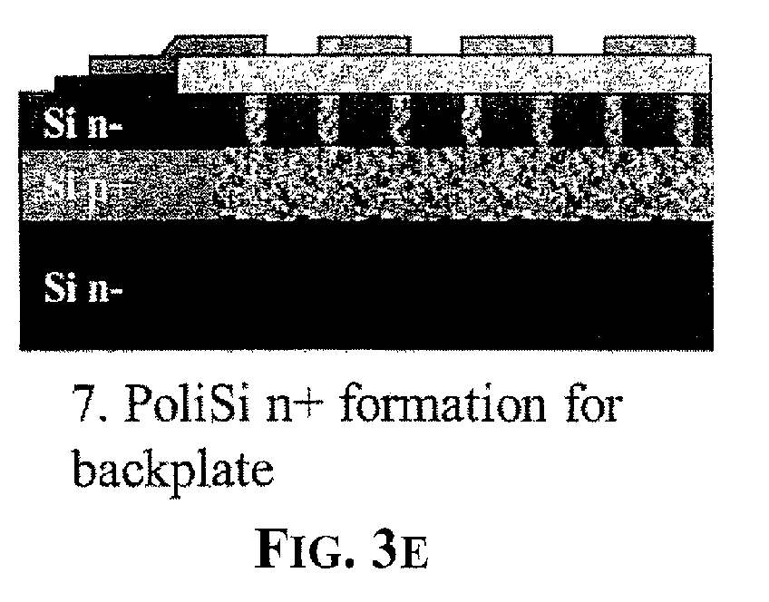
- a backplate structure of the sensor is formed according to the known technique of first depositing by a PVAPOX process a layer of sacrificial oxide over the sensor area followed by the deposition of a contouring layer of silicon nitride around the perimeter sacrificial oxide layer and finally depositing layer of polycrystalline silicon of backplate with a plurality of holes over the sacrificial oxide layer and over the perimetral layer of silicon nitride.
- the backplate of polysilicon must be pervious to pressure waves through its plurality of uniformely spaced holes in order to allow a correct action of the pressure wave on the diaphragm, from the surface of which it must be sufficiently spaced to accomodate an unrestrained maximum deflection of the diaphragm according to the established dynamic range thereof.
- the gap between the diaphragm (epi) and the backplate or grid (n+poly) may be of about 1 ⁇ m.
- the polysilicon backplate should have a conductivity sufficient to act as second plate of a capacitor, a first plate of which is constituted by the vibrating diaphragm itself.
- the polysilicon backplate is n + doped and rests on the perimetral isolation layer of silicon nitride.
- a second layer of undoped polysilicon may be deposited over the n + doped layer (conductive plate) for mechanical protection and electric isolation purposes.
- the layer of sacrifical oxide is then removed by isotropic chemical etching through the holes of the polysilicon backplate layer, that will eventually rest on the perimetral supporting layer of silicon nitride.
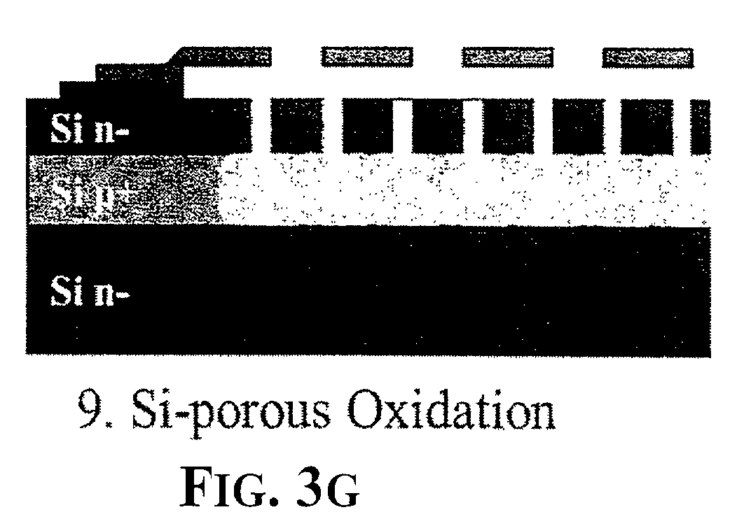
- a microphonic cavity is realized by chemically etching off the PVAPOX silicon oxide that sealed the trenches, by thermally oxidizing the porous silicon of the buried layer and leaching it away chemically through the re-opened trenches.
- the porous silicon of the buried layer may be oxidized immediately after having rendered porous by the selective electrochemical etching and continuing the process by sealing the trenches, planarizing the surface and forming the backplate structure of polysilicon.
- the pressure sensors of this invention are entirely made in a monolithic form.
- the depth of the microphonic cavity of the pressure sensor of this invention may be established simply by varying the thickness of the doped buried layer to be eventually etched away.
- the microphonic cavity is realized by dissolving the oxidized porous silicon (that is the oxide), a processing step that may be safely performed at room temperature using a diluted solution of hydrofluoric acid.
- the known processes rely on a chemical etching of the monocrystalline silicon of the substrate that must be carried out at a temperature of at least about 85-90°C because of the unacceptably low rate of the etching at room temperature of monocrystalline silicon.
- the diaphragm of the pressure sensor constituted by the epitaxial layer overhanging on the microphonic cavity formed with the method of this invention may have any shape, for example it may be in have the form of concentric circular sectors, each 100 ⁇ m wide, as depicted in Fig. 5.
- the pressure sensor of the invention may be easily integrated using common processing techniques by carrying out a sequence of process steps for selectively making porous the silicon of the doped buried layer, after which common processing steps may follow (for instance according to a standard CMOS process), for realizing the circuitry with which the pressure sensor will interact.
- a further object of the invention is that of providing a monolithically integrated system, as the one depicted in Fig. 6, for sensing the direction of provenance of a sound wave and its intensity by analyzing the signals produced by an array of monolithically integrated pressure sensors of the invention, disposed at different locations of the same chip.
- the distinct pressure sensors of the system which in the embodiment of Fig. 6 are only two but which may be even more numerous, will produce at different instants an electric signal representative of the vibration induced on their diaphragm.
- the direction of provenance of a sound wave as sensed by the various pressure sensors of the integrated system of the invention is determined on the basis of the relative delays with which distinct sensors detect the sound wave.
- This may be implemented by carrying out a time-delay correlation between the signal produced by a first sensor and the signal produced by any other sensor present in the integrated device and calculating for which delays the correlations are at their maximum. Each of these delays will represent the difference between the times needed by the sound wave to reach the respective sensor. Knowing the relative positions of the various sensors, it is possible to evaluate by triangulation the direction of provenience of the sound wave.
Abstract


Description
- The present invention relates in general to pressure sensors and in particular to an integrated pressure sensor and a relative process of fabrication by means of surface micromachining.
- Pressure sensors are used in several applications, particularly in processes of active noise cancellation, especially in distributed parameters systems such as an airplane cabin or the interior of a vehicle.
- Semiconductor pressure sensors are widely used for these purposes. Their sensing element is a vibrating silicon diaphragm topped by a spaced backplate layer provided with a plurality of openings of polycrystalline silicon (polysilicon or briefly "poly"), both disposed over a microphonic cavity.
- These pressure sensors are constructed starting from a semiconductor structure obtained by defining the area of the pressure sensor and implanting a dopant to form a doped layer of a certain type in a monocrystalline silicon substrate of doping type opposite to that of the doped layer that is finally created as a doped buried layer upon growing an epitaxial layer of the same type of doping of the substrate thereon. The epitaxial layer in the area of the sensor will eventually become the diaphragm of the sensor.
- By "etching from the substrate", that is etching the substrate from the back side thereof as far as reaching the buried doped layer, the latter is uncovered and thereafter selectively etched to leave a microphonic diaphragm constituted by the epitaxial layer overhanging on a so realized cavity (microphonic cavity).
- This known technique requires that the mask or masks used to carry out the etchings on the back side of the substrate must be perfectly aligned with the masks that are normally used on the front side of the semiconductor wafer for realizing a suitable backplate structure of the pressure sensor above the diaphragm.
- This is an unavoidable drawback because of the special equipments that are needed, the relatively poor precision of alignment that can be achieved and the relatively high costs.
- Moreover the selective chemical etching of the buried doped silicon layer must be carried out at a relatively high temperature (in the range of 85-90°C), typically using an acqueous solution of potassium hydroxide KOH, in order to achieve a sufficiently fast etching rate.
- A further drawback of the known process consists in that the etching rate (microns of material removed per minute) in a direction normal to the plane of the substrate is typically of 0.3 µm/min, while the speed of the etching in a direction parallel to the plane of the substrate is of about 0.03 µm/min, that is ten times smaller. This produces a typically V-shaped groove, as depicted in Fig. 1.
- Such a V-shaped cross section of the microphonic cavity may be observed in known semiconductor microphones of different kind, such as those depicted in Fig. 2, whether they are piezoresistive (a), piezoelectric (b), capacitive (c) or optically read (d), and represents a tolerated but far from optimal shape because of the disuniformity of pressure wave reactions over the microphonic sensible area.
- The rear of the microphonic cavity is successively closed by the so called "wafer bonding" technique, that is the so realized sensor is "bonded" onto a flat silicon wafer, in which the relative circuitry may be integrated.
- A method for realizing integrated CMOS structures, by first realizing portions of circuits on a separate wafer and thereafter carrying out a wafer bonding, is described in the US Patent No. 5,659,195.
- In practice the above described known process, which is relatively complicated by the wafer bonding step, does not provide for a monolithically integrable pressure sensor as it would be desirable under for many respects. Moreover, it is not possible to vary the depth of the microphonic cavity that is pre-determined by the thickness of the substrate.
- It has been found and is the object of the invention a process for realizing pressure sensors monolithically integrable together with a semiconductor integrated circuit on the same chip, overcoming the above mentioned limits and drawbacks of prior art techniques.
- According to the present invention, monolithically integrated pressure sensors of outstanding quality and versatility are produced through micromechanical surface structures definition techniques, typical of MEMS (MicroElectroMechanical Systems).
- More precisely the object of the invention is a process of fabrication of a pressure sensor that comprises forming in a monocrystalline silicon substrate of a certain type of conductivity a buried layer of opposite type of conductivity upon growing an epitaxial layer of the same type of conductivity of the substrate, forming a sacrifical layer of oxide over the epitaxial layer, forming a polysilicon backplate layer with a plurality of holes above the area of the sensor on the sacrifical oxide layer, chemically etching the sacrifical oxide layer through the holes of the polysilicon backplate layer removing the oxide in the sensor area and forming a microphonic cavity in the sensor area under the epitaxial layer diaphragm by selectively etching the doped silicon of said buried layer.
- Differently from the known processes, according to this invention, a microphonic cavity in the semiconductor substrate is monolithically formed by carrying out the following steps before forming the sacrifical oxide layer:
- 1) cutting by plasma etching the front side or the back side of the silicon wafer a plurality of trenches or holes deep enough to extend for at least part of its thickness into said buried layer to be selectively etched;
- 2) electrochemically etching through such trenches, the silicon of said buried layer with an electrolytic solution suitable for selectively etching the doped silicon of said opposite type of conductivity, making the silicon of the buried layer porous;
- 3) oxidizing and leaching away the silicon so made porous.
-
- Narrow trenches or holes, reaching into the buried layer are realized in the first step, while in the second step the silicon of the buried layer is rendered highly porous. The so made porous silicon may be then easily oxidized and a final chemical etching of the oxidized silicon may be carried out at significantly lower temperatures than those that are normally required by prior art techniques based on the selective etching of the doped monocrystalline silicon.
- The trenches or holes for accessing the doped buried layer may even be cut through the epitaxial layer and not through the rear of the monocrystalline silicon substrate thus avoiding the burden of precisely aligning the mask on the rear surface with the masks that are used on the front surface of the substrate. Moreover, the thickness of the substrate is normally greater than that of the epitaxial layer and thus the need to cut relatively deep and narrow trenches requiring the use of special plasma etching equipment is avoided.
- Optionally, the porous silicon of the buried layer may be oxidized immediately after having performed the selective electrochemical etching or it may be oxidized later in the process, after having deposited the polysilicon layer of backplate.
- A further advantage of the present invention is to provide pressure sensors with a cavity that may be wholly defined in a monolithic semiconducting substrate and whose shape and dimensions may be freely established and with a diaphragm that may be shaped in any desired manner leaving to the designer an unrestrained choice of layout.
- A further advantage of the invention is that of allowing the realization of a monolithically integrated system for detecting the direction of provenance of a sound wave, capable of exploiting to this end an array of integrated pressure sensors of the invention disposed according to a certain layout.
- The invention is more precisely defined in the appended claims.
- The different aspects and advantages of the invention will become even more evident through a detailed description of an embodiment of the invention and by referring to the attached drawings, wherein:
- Figure 1 depicts a monolithic substrate with an integrated diaphragm realized using the known technique of etching the substrate from the back;
- Figure 2 is a collection of pressure sensors of different types realized by etching the substrate from the back;
- Figures from 3a to 3h illustrate different steps of the process of the invention according to a preferred embodiment;
- Figure 4 is a possible layout of an integrated pressure sensor of the invention;
- Figure 5 is a basic circuit diagram of an integrated system for sensing the direction of provenience of a sound wave.
-
- With the process of this invention, the fundamental steps of which are schematically illustrated in Fig. 3, a monolithically integrated pressure sensor is constructed by surface micromachining techniques using a relatively low temperature etching of the doped monocrystalline silicon.
- First, in the defined sensor area, a buried layer of doping of opposite type of conductivity is realized in a doped monocrystalline silicon substrate upon growing thereon a doped epitaxial layer of the same type of conductivity of the substrate.
- In the example illustrated in Fig. 3, the buried layer has a P+ doping while the substrate and the epitaxial layer are both N- doped, though the invention may be practiced even by inverting the types of doping.
- According to the embodiment shown by way of example in Fig. 3, a plurality of narrow and deep trenches are cut through the epitaxial layer and through part of the thickness of the previously formed buried layer by masking and anisotropically plasma etching. The width of the trenches may be in the range of 3 to 6 µm.
- According to this preferred embodiment, the trenches are cut starting from the front of the wafer thus facilitating mask alignment.
- The trenches cut from the front of the wafer through the epitaxial layer that will ultimately become the diaphragm of dynamic pressure sensor (pressure wave sensor) must be wide enough to permit electrochemical etching of the silicon of the doped buried layer and the subsequent oxidation of the porous silicon and its chemical leaching away, permit a relief of the air from the microphonic cavity when the diaphragm flexes inwardly under the effect of the crest of a pressure wave.
- Overall, the size and distribution of the trenches or holes through the epitaxial layer (diaphragm of the sensor) must be designed, on account of the thickness of the layer, such to confer to the diaphragm the desired characteristics of flexibility, sturdiness and vibrational modes.
- In any case, these narrow trenches are made deep enough to extend for at least a portion of its thickness into the buried layer.
- The doped silicon buried layer is selectively etched electrochemically using an electrolytic solution suited to selectively or preferentially dissolve the P doped silicon, making the silicon of the buried layer porous. Preferably an acqueous solution of hydrofluoric acid (HF).
- Thereafter, the trenches are sealed by depositing a silicon oxide layer by a PVAPOX process and the surface is planarized according to common techniques.
- On the so planarized surface a backplate structure of the sensor is formed according to the known technique of first depositing by a PVAPOX process a layer of sacrificial oxide over the sensor area followed by the deposition of a contouring layer of silicon nitride around the perimeter sacrificial oxide layer and finally depositing layer of polycrystalline silicon of backplate with a plurality of holes over the sacrificial oxide layer and over the perimetral layer of silicon nitride.
- The backplate of polysilicon must be pervious to pressure waves through its plurality of uniformely spaced holes in order to allow a correct action of the pressure wave on the diaphragm, from the surface of which it must be sufficiently spaced to accomodate an unrestrained maximum deflection of the diaphragm according to the established dynamic range thereof. Normally the gap between the diaphragm (epi) and the backplate or grid (n+poly) may be of about 1 µm.
- Moreover, the polysilicon backplate should have a conductivity sufficient to act as second plate of a capacitor, a first plate of which is constituted by the vibrating diaphragm itself.
- According to the embodiment shown, the polysilicon backplate is n + doped and rests on the perimetral isolation layer of silicon nitride. Optionally a second layer of undoped polysilicon may be deposited over the n + doped layer (conductive plate) for mechanical protection and electric isolation purposes.
- The layer of sacrifical oxide is then removed by isotropic chemical etching through the holes of the polysilicon backplate layer, that will eventually rest on the perimetral supporting layer of silicon nitride.
- Finally, a microphonic cavity is realized by chemically etching off the PVAPOX silicon oxide that sealed the trenches, by thermally oxidizing the porous silicon of the buried layer and leaching it away chemically through the re-opened trenches.
- Optionally, the porous silicon of the buried layer may be oxidized immediately after having rendered porous by the selective electrochemical etching and continuing the process by sealing the trenches, planarizing the surface and forming the backplate structure of polysilicon.
- Contrary to the sensors of the CMOS device described in the US Patent No.5,659,195, wherein the microphonic cavity is closed by "wafer bonding" technique, the pressure sensors of this invention are entirely made in a monolithic form.
- The depth of the microphonic cavity of the pressure sensor of this invention may be established simply by varying the thickness of the doped buried layer to be eventually etched away.
- According to the process of the invention, the microphonic cavity is realized by dissolving the oxidized porous silicon (that is the oxide), a processing step that may be safely performed at room temperature using a diluted solution of hydrofluoric acid. By contrast, the known processes rely on a chemical etching of the monocrystalline silicon of the substrate that must be carried out at a temperature of at least about 85-90°C because of the unacceptably low rate of the etching at room temperature of monocrystalline silicon.
- The diaphragm of the pressure sensor constituted by the epitaxial layer overhanging on the microphonic cavity formed with the method of this invention may have any shape, for example it may be in have the form of concentric circular sectors, each 100 µm wide, as depicted in Fig. 5.
- The pressure sensor of the invention may be easily integrated using common processing techniques by carrying out a sequence of process steps for selectively making porous the silicon of the doped buried layer, after which common processing steps may follow (for instance according to a standard CMOS process), for realizing the circuitry with which the pressure sensor will interact.
- A further object of the invention is that of providing a monolithically integrated system, as the one depicted in Fig. 6, for sensing the direction of provenance of a sound wave and its intensity by analyzing the signals produced by an array of monolithically integrated pressure sensors of the invention, disposed at different locations of the same chip.
- The distinct pressure sensors of the system, which in the embodiment of Fig. 6 are only two but which may be even more numerous, will produce at different instants an electric signal representative of the vibration induced on their diaphragm. The direction of provenance of a sound wave as sensed by the various pressure sensors of the integrated system of the invention is determined on the basis of the relative delays with which distinct sensors detect the sound wave.
- This may be implemented by carrying out a time-delay correlation between the signal produced by a first sensor and the signal produced by any other sensor present in the integrated device and calculating for which delays the correlations are at their maximum. Each of these delays will represent the difference between the times needed by the sound wave to reach the respective sensor. Knowing the relative positions of the various sensors, it is possible to evaluate by triangulation the direction of provenience of the sound wave.
Claims (8)
- A process of fabrication of a pressure sensor comprising the steps of forming a buried layer of a second type of conductivity (Si_P+) in a monocrystalline silicon substrate (Si_N-) of a first type of conductivity upon growing an epitaxial layer (N_Si) of said first type of conductivity, depositing a sacrificial oxide layer on said epitaxial layer (N_Si) in the area of said sensor, depositing a polysilicon layer of backplate provided with a plurality of holes over said sacrificial oxide layer, isotropically etching said sacrificial oxide layer through said holes as far as removing the oxide in the sensor area and forming a microphonic cavity under said epitaxial layer in the sensor area, characterized in that before depositing said sacrifical oxide layer the method comprises the steps of:and after having deposited said polysilicon layer of backplate and removed said sacrifical oxide the method comprises the steps ofdefining by masking and cutting a plurality of trenches or holes uniformly spaced from one another by anisotropic plasma etching the monocrystalline silicon either from the front side or through the rear side for a depth sufficient to reach through at least a portion of the thickness of said doped buried layer over the area of the sensor;electrochemically etching the doped silicon (Si_P+) of said buried layer through said trenches using an electrolytic solution adapted for selectively dissolving the doped silicon of said opposite kind of conductivity, making porous the silicon of said buried layer;sealing said trenches or holes by depositing a layer of sealant material;selectively etching said sealant material reopening said trenches or holes;oxidizing the porous silicon of said buried layer and chemically etching the oxidized silicon with an acid solution through the reopened trenches or holes realizing said microphone cavity underneath the epitaxial layer.
- The process according to claim 1, wherein said acid solution is a diluted solution of hydrofluoric acid and the etching is carried out at room temperature.
- The process according to claim 1, wherein said sealing material and said sacrifical oxide is silicon oxide deposited by a PVAPOX technique.
- The process according to claim 1, wherein said cavity and overhanging diaphragm are shaped as concentric circular sectors.
- The process according to claim 1, wherein said of oxidation step is carried out immediately after the electrochemical etching of the silicon of the buried layer.
- A pressure sensor defined on a monocrystalline silicon substrate and including a microphonic cavity a monocrystalline silicon diaphragm closing said cavity and a polycrystalline silicon backplate layer, spaced from said monocrystalline silicon diaphragm and having a plurality of holes overhanging on said diaphragm, characterized in that said pressure sensor is in monolithic form.
- The pressure sensor of claim 6, wherein said backplate layer is composed of a first polycrystalline silicon layer with a doping of the same type of conductivity of the substrate and of said epitaxial layer, topped by a second layer of undoped polycrystalline silicon.
- A monolithically integrated system for detecting the direction of provenance of a sound wave comprisinga plurality of pressure sensors according to anyone of claims 6 and 7, disposed according to a certain layout on the chip and producing respective analog signals;as many analog/digital converters of the signals produced by the respective sensors, generating respectively corresponding digital signals;calculating means performing a time-delay correlation between the digital signal produced by a first sensor and the digital signal of another sensor generating a value of delay for which the correlation is maximum;a microprocessor calculating the direction of provenance of the sound wave as sensed by the pressure sensors in function of said delay values.
Applications Claiming Priority (2)
| Application Number | Priority Date | Filing Date | Title |
|---|---|---|---|
| ITVA000042 | 2000-12-15 | ||
| IT2000VA000042A ITVA20000042A1 (en) | 2000-12-15 | 2000-12-15 | MONOLITHICALLY INTEGRATED PRESSURE SENSOR AND RELATED DIRECTION PROCESS. |
Publications (2)
| Publication Number | Publication Date |
|---|---|
| EP1215476A2 true EP1215476A2 (en) | 2002-06-19 |
| EP1215476A3 EP1215476A3 (en) | 2003-09-17 |
Family
ID=11460830
Family Applications (1)
| Application Number | Title | Priority Date | Filing Date |
|---|---|---|---|
| EP01830759A Withdrawn EP1215476A3 (en) | 2000-12-15 | 2001-12-12 | Pressure sensor monolithically integrated and relative process of fabrication |
Country Status (3)
| Country | Link |
|---|---|
| US (1) | US6743654B2 (en) |
| EP (1) | EP1215476A3 (en) |
| IT (1) | ITVA20000042A1 (en) |
Cited By (6)
| Publication number | Priority date | Publication date | Assignee | Title |
|---|---|---|---|---|
| WO2007137893A1 (en) * | 2006-05-26 | 2007-12-06 | Robert Bosch Gmbh | Micromechanic component and method for the production thereof |
| WO2008131981A2 (en) * | 2007-04-26 | 2008-11-06 | Robert Bosch Gmbh | Micromechanical membrane sensor with reduced stray capacitance and corresponding production method |
| GB2452877A (en) * | 2006-03-20 | 2009-03-18 | Wolfson Microelectronics Plc | Fabrication of MEMS capacitive microphone |
| EP2275946A1 (en) | 2005-03-04 | 2011-01-19 | STMicroelectronics S.r.l. | Probabilistic neural network and relative training method |
| WO2013089845A2 (en) * | 2011-09-14 | 2013-06-20 | Analog Devices, Inc. | Method for etching material longitudinally spaced from etch mask |
| US8586451B2 (en) | 2011-06-27 | 2013-11-19 | Stmicroelectronics S.R.L. | Flexible electronic device and method for the fabrication of same |
Families Citing this family (41)
| Publication number | Priority date | Publication date | Assignee | Title |
|---|---|---|---|---|
| DE10114036A1 (en) * | 2001-03-22 | 2002-10-02 | Bosch Gmbh Robert | Process for the production of micromechanical sensors and sensors produced therewith |
| FR2823998B1 (en) * | 2001-04-25 | 2004-01-02 | Centre Nat Rech Scient | BIOSENSOR MATRIX AND MANUFACTURING METHOD THEREOF |
| US7045459B2 (en) * | 2002-02-19 | 2006-05-16 | Northrop Grumman Corporation | Thin film encapsulation of MEMS devices |
| DE10305442A1 (en) * | 2003-02-11 | 2004-08-19 | Robert Bosch Gmbh | A process for preparation of a micromechanical device with a substrate, a membrane, and a hollow space by etching useful in electronics for thermal decoupling between structural elements and substrates |
| US7335971B2 (en) * | 2003-03-31 | 2008-02-26 | Robert Bosch Gmbh | Method for protecting encapsulated sensor structures using stack packaging |
| US7172917B2 (en) | 2003-04-17 | 2007-02-06 | Robert Bosch Gmbh | Method of making a nanogap for variable capacitive elements, and device having a nanogap |
| US7569412B2 (en) * | 2003-12-16 | 2009-08-04 | Robert Bosch Gmbh | Method for manufacturing a diaphragm sensor |
| DE102004036035B4 (en) * | 2003-12-16 | 2015-10-15 | Robert Bosch Gmbh | Method for producing a semiconductor component and a semiconductor component, in particular a membrane sensor |
| EP1544163B1 (en) * | 2003-12-16 | 2021-02-24 | Robert Bosch GmbH | Method for producing a membrane sensor and corresponding membrane sensor |
| US7491566B2 (en) * | 2004-02-09 | 2009-02-17 | Analog Devices, Inc. | Method of forming a device by removing a conductive layer of a wafer |
| DE102004043357B4 (en) * | 2004-09-08 | 2015-10-22 | Robert Bosch Gmbh | Method for producing a micromechanical sensor element |
| DE102004058879B4 (en) * | 2004-12-06 | 2013-11-07 | Austriamicrosystems Ag | MEMS microphone and method of manufacture |
| WO2006060937A1 (en) * | 2004-12-10 | 2006-06-15 | Shanghai Institute Of Microsystem And Information Technology, Chinese Academy Of Sciences | A mems device including a laterally movable portion wiht piezo-resistive sensing elements and electrostatic actuating elements on trench side walls and methods for producing the same |
| JP2006278674A (en) * | 2005-03-29 | 2006-10-12 | Nec Electronics Corp | Field effect transistor and its manufacturing method, and semiconductor device |
| US7449356B2 (en) * | 2005-04-25 | 2008-11-11 | Analog Devices, Inc. | Process of forming a microphone using support member |
| US8043950B2 (en) | 2005-10-26 | 2011-10-25 | Semiconductor Energy Laboratory Co., Ltd. | Semiconductor device and manufacturing method thereof |
| US8153318B2 (en) | 2006-11-08 | 2012-04-10 | Alan Devoe | Method of making a fuel cell device |
| DE102005056759A1 (en) * | 2005-11-29 | 2007-05-31 | Robert Bosch Gmbh | Micromechanical structure for use as e.g. microphone, has counter units forming respective sides of structure, where counter units have respective electrodes, and closed diaphragm is arranged between counter units |
| DE102006001493B4 (en) * | 2006-01-11 | 2007-10-18 | Austriamicrosystems Ag | MEMS sensor and method of manufacture |
| US8029937B2 (en) | 2006-05-11 | 2011-10-04 | Alan Devoe | Solid oxide fuel cell device and system |
| JP2010506532A (en) * | 2006-10-11 | 2010-02-25 | メムス テクノロジー ビーエイチディー | Extremely low pressure sensor and method for manufacturing the same |
| JP2008188711A (en) * | 2007-02-05 | 2008-08-21 | Oki Electric Ind Co Ltd | Semiconductor device manufacturing method |
| US7736929B1 (en) | 2007-03-09 | 2010-06-15 | Silicon Clocks, Inc. | Thin film microshells incorporating a getter layer |
| US7923790B1 (en) * | 2007-03-09 | 2011-04-12 | Silicon Laboratories Inc. | Planar microshells for vacuum encapsulated devices and damascene method of manufacture |
| US7595209B1 (en) * | 2007-03-09 | 2009-09-29 | Silicon Clocks, Inc. | Low stress thin film microshells |
| US7659150B1 (en) | 2007-03-09 | 2010-02-09 | Silicon Clocks, Inc. | Microshells for multi-level vacuum cavities |
| CN101346014B (en) * | 2007-07-13 | 2012-06-20 | 清华大学 | Micro electro-mechanical system microphone and preparation method thereof |
| DE102008001185A1 (en) * | 2008-04-15 | 2009-10-29 | Robert Bosch Gmbh | Process for producing a micromechanical membrane structure with a fixed counter element |
| JP5374077B2 (en) * | 2008-06-16 | 2013-12-25 | ローム株式会社 | MEMS sensor |
| JP4726927B2 (en) * | 2008-06-19 | 2011-07-20 | 株式会社日立製作所 | Integrated microelectromechanical system and manufacturing method thereof |
| US7999635B1 (en) | 2008-07-29 | 2011-08-16 | Silicon Laboratories Inc. | Out-of plane MEMS resonator with static out-of-plane deflection |
| DE102008042258A1 (en) * | 2008-09-22 | 2010-04-01 | Robert Bosch Gmbh | Method for producing a micromechanical chip and a component with such a chip |
| US8134215B2 (en) * | 2008-10-09 | 2012-03-13 | United Microelectronics Corp. | MEMS diaphragm |
| JP2010098518A (en) * | 2008-10-16 | 2010-04-30 | Rohm Co Ltd | Method of manufacturing mems sensor, and mems sensor |
| US8643128B2 (en) * | 2009-02-24 | 2014-02-04 | Pixart Imaging Incorporation | Micro-electro-mechanical-system sensor and method for making same |
| US8975671B2 (en) * | 2010-01-11 | 2015-03-10 | Elmos Semiconductor Ag | Microelectromechanical semiconductor component that is sensitive to mechanical stresses, and comprises an ion implantation masking material defining a channel region |
| US8316717B2 (en) * | 2010-06-29 | 2012-11-27 | Rogue Valley Microdevices, Inc. | Wireless self-powered monolithic integrated capacitive sensor and method of manufacture |
| TWI439413B (en) | 2011-03-30 | 2014-06-01 | Pixart Imaging Inc | Mems sensing device and method for making same |
| US8471641B2 (en) | 2011-06-30 | 2013-06-25 | Silicon Laboratories Inc. | Switchable electrode for power handling |
| US9181086B1 (en) | 2012-10-01 | 2015-11-10 | The Research Foundation For The State University Of New York | Hinged MEMS diaphragm and method of manufacture therof |
| US9422149B2 (en) | 2014-07-25 | 2016-08-23 | Semiconductor Manufacturing International (Shanghai) Corporation | Trapped sacrificial structures and methods of manufacturing same using thin-film encapsulation |
Family Cites Families (6)
| Publication number | Priority date | Publication date | Assignee | Title |
|---|---|---|---|---|
| US5725729A (en) * | 1994-09-26 | 1998-03-10 | The Charles Stark Draper Laboratory, Inc. | Process for micromechanical fabrication |
| JP3399660B2 (en) * | 1994-10-06 | 2003-04-21 | 株式会社東海理化電機製作所 | Manufacturing method of surface type acceleration sensor |
| US5659195A (en) * | 1995-06-08 | 1997-08-19 | The Regents Of The University Of California | CMOS integrated microsensor with a precision measurement circuit |
| US5573679A (en) * | 1995-06-19 | 1996-11-12 | Alberta Microelectronic Centre | Fabrication of a surface micromachined capacitive microphone using a dry-etch process |
| EP0822398B1 (en) | 1996-07-31 | 2003-04-23 | STMicroelectronics S.r.l. | Integrated piezoresistive pressure sensor and relative fabrication method |
| US6472244B1 (en) * | 1996-07-31 | 2002-10-29 | Sgs-Thomson Microelectronics S.R.L. | Manufacturing method and integrated microstructures of semiconductor material and integrated piezoresistive pressure sensor having a diaphragm of polycrystalline semiconductor material |
-
2000
- 2000-12-15 IT IT2000VA000042A patent/ITVA20000042A1/en unknown
-
2001
- 2001-12-11 US US10/014,880 patent/US6743654B2/en not_active Expired - Lifetime
- 2001-12-12 EP EP01830759A patent/EP1215476A3/en not_active Withdrawn
Non-Patent Citations (1)
| Title |
|---|
| None * |
Cited By (17)
| Publication number | Priority date | Publication date | Assignee | Title |
|---|---|---|---|---|
| EP2275946A1 (en) | 2005-03-04 | 2011-01-19 | STMicroelectronics S.r.l. | Probabilistic neural network and relative training method |
| US7856804B2 (en) | 2006-03-20 | 2010-12-28 | Wolfson Microelectronics Plc | MEMS process and device |
| GB2452877B (en) * | 2006-03-20 | 2009-09-30 | Wolfson Microelectronics Plc | Mems process and device |
| GB2452877A (en) * | 2006-03-20 | 2009-03-18 | Wolfson Microelectronics Plc | Fabrication of MEMS capacitive microphone |
| GB2452876A (en) * | 2006-03-20 | 2009-03-18 | Wolfson Microelectronics Plc | MEMES capacitive microphone |
| US7781249B2 (en) | 2006-03-20 | 2010-08-24 | Wolfson Microelectronics Plc | MEMS process and device |
| GB2452876B (en) * | 2006-03-20 | 2010-10-13 | Wolfson Microelectronics Plc | Mems process and device |
| WO2007137893A1 (en) * | 2006-05-26 | 2007-12-06 | Robert Bosch Gmbh | Micromechanic component and method for the production thereof |
| US8165324B2 (en) | 2006-05-26 | 2012-04-24 | Robert Bosch Gmbh | Micromechanical component and method for its production |
| WO2008131981A2 (en) * | 2007-04-26 | 2008-11-06 | Robert Bosch Gmbh | Micromechanical membrane sensor with reduced stray capacitance and corresponding production method |
| WO2008131981A3 (en) * | 2007-04-26 | 2009-01-08 | Bosch Gmbh Robert | Micromechanical membrane sensor with reduced stray capacitance and corresponding production method |
| US8558327B2 (en) | 2007-04-26 | 2013-10-15 | Robert Bosch Gmbh | Micromechanical component and corresponding production method |
| US8586451B2 (en) | 2011-06-27 | 2013-11-19 | Stmicroelectronics S.R.L. | Flexible electronic device and method for the fabrication of same |
| WO2013089845A2 (en) * | 2011-09-14 | 2013-06-20 | Analog Devices, Inc. | Method for etching material longitudinally spaced from etch mask |
| WO2013089845A3 (en) * | 2011-09-14 | 2013-10-03 | Analog Devices, Inc. | Method for etching material longitudinally spaced from etch mask |
| CN103917484A (en) * | 2011-09-14 | 2014-07-09 | 应美盛股份有限公司 | Method for etching material longitudinally spaced from etch mask |
| CN103917484B (en) * | 2011-09-14 | 2016-06-15 | 应美盛股份有限公司 | For the method etching the material longitudinally-spaced with etching mask |
Also Published As
| Publication number | Publication date |
|---|---|
| US6743654B2 (en) | 2004-06-01 |
| EP1215476A3 (en) | 2003-09-17 |
| ITVA20000042A1 (en) | 2002-06-15 |
| US20020151100A1 (en) | 2002-10-17 |
Similar Documents
| Publication | Publication Date | Title |
|---|---|---|
| US6743654B2 (en) | Method of fabricating pressure sensor monolithically integrated | |
| US9458009B2 (en) | Semiconductor devices and methods of forming thereof | |
| US5888412A (en) | Method for making a sculptured diaphragm | |
| US7545012B2 (en) | Capacitive micromachined ultrasound transducer fabricated with epitaxial silicon membrane | |
| EP2536168B1 (en) | Epitaxial silicon CMOS-MEMS microphone and method for manufacturing | |
| JP5113980B2 (en) | Pressure sensor device and manufacturing method thereof | |
| KR101080496B1 (en) | Micromechanical capacitive pressure transducer and production method | |
| US7214324B2 (en) | Technique for manufacturing micro-electro mechanical structures | |
| KR100964971B1 (en) | Micro piezoresistive pressure sensor and manufacturing method thereof | |
| JP5222399B2 (en) | Manufacturing method of membrane structure by micromechanical technology accessed from backside of substrate | |
| US20080185669A1 (en) | Silicon Microphone | |
| KR100348177B1 (en) | Isolation Method for Single Crystalline Silicon Micro Machining using Deep Trench Dielectric Layer | |
| US6357299B1 (en) | Micromechanical sensor and method for producing the same | |
| US20020001871A1 (en) | Triple layer isolation for silicon microstructure and structures formed using the same | |
| KR20010072390A (en) | Micromechanical sensor and corresponding production method | |
| JP2005062196A (en) | Micromechanics sensor and its manufacturing method | |
| JPH05343704A (en) | Manufacture of boss diaphragm structure body embedded inside silicon | |
| US6503775B2 (en) | Production method of a micromachine | |
| US7833405B2 (en) | Micromechanical component and corresponding production method | |
| JP2000155030A (en) | Manufacture of angular velocity sensor | |
| JP2000124465A (en) | Manufacture of semiconductor dynamical amount sensor | |
| US7179668B2 (en) | Technique for manufacturing silicon structures | |
| JP3055508B2 (en) | Manufacturing method of pressure detector | |
| JP3428179B2 (en) | Semiconductor diaphragm structure and method for manufacturing semiconductor diaphragm | |
| CN114506811A (en) | MEMS device and manufacturing method thereof |
Legal Events
| Date | Code | Title | Description |
|---|---|---|---|
| PUAI | Public reference made under article 153(3) epc to a published international application that has entered the european phase |
Free format text: ORIGINAL CODE: 0009012 |
|
| AK | Designated contracting states |
Kind code of ref document: A2 Designated state(s): AT BE CH CY DE DK ES FI FR GB GR IE IT LI LU MC NL PT SE TR |
|
| AX | Request for extension of the european patent |
Free format text: AL;LT;LV;MK;RO;SI |
|
| PUAL | Search report despatched |
Free format text: ORIGINAL CODE: 0009013 |
|
| AK | Designated contracting states |
Kind code of ref document: A3 Designated state(s): AT BE CH CY DE DK ES FI FR GB GR IE IT LI LU MC NL PT SE TR |
|
| AX | Request for extension of the european patent |
Extension state: AL LT LV MK RO SI |
|
| RIC1 | Information provided on ipc code assigned before grant |
Ipc: 7G 01L 9/00 B Ipc: 7G 01L 9/06 A |
|
| 17P | Request for examination filed |
Effective date: 20040305 |
|
| AKX | Designation fees paid |
Designated state(s): DE FR GB IT |
|
| 17Q | First examination report despatched |
Effective date: 20061211 |
|
| STAA | Information on the status of an ep patent application or granted ep patent |
Free format text: STATUS: THE APPLICATION HAS BEEN WITHDRAWN |
|
| 18W | Application withdrawn |
Effective date: 20080311 |