EP1213756A2 - Fabrication process of semiconductor package and semiconductor package - Google Patents
Fabrication process of semiconductor package and semiconductor package Download PDFInfo
- Publication number
- EP1213756A2 EP1213756A2 EP02003794A EP02003794A EP1213756A2 EP 1213756 A2 EP1213756 A2 EP 1213756A2 EP 02003794 A EP02003794 A EP 02003794A EP 02003794 A EP02003794 A EP 02003794A EP 1213756 A2 EP1213756 A2 EP 1213756A2
- Authority
- EP
- European Patent Office
- Prior art keywords
- wiring
- semiconductor
- supporting member
- mounting
- substrate
- Prior art date
- Legal status (The legal status is an assumption and is not a legal conclusion. Google has not performed a legal analysis and makes no representation as to the accuracy of the status listed.)
- Withdrawn
Links
Images


Classifications
-
- H—ELECTRICITY
- H01—ELECTRIC ELEMENTS
- H01L—SEMICONDUCTOR DEVICES NOT COVERED BY CLASS H10
- H01L21/00—Processes or apparatus adapted for the manufacture or treatment of semiconductor or solid state devices or of parts thereof
- H01L21/02—Manufacture or treatment of semiconductor devices or of parts thereof
- H01L21/04—Manufacture or treatment of semiconductor devices or of parts thereof the devices having at least one potential-jump barrier or surface barrier, e.g. PN junction, depletion layer or carrier concentration layer
- H01L21/50—Assembly of semiconductor devices using processes or apparatus not provided for in a single one of the subgroups H01L21/06 - H01L21/326, e.g. sealing of a cap to a base of a container
- H01L21/56—Encapsulations, e.g. encapsulation layers, coatings
- H01L21/568—Temporary substrate used as encapsulation process aid
-
- H—ELECTRICITY
- H01—ELECTRIC ELEMENTS
- H01L—SEMICONDUCTOR DEVICES NOT COVERED BY CLASS H10
- H01L23/00—Details of semiconductor or other solid state devices
- H01L23/12—Mountings, e.g. non-detachable insulating substrates
-
- H—ELECTRICITY
- H01—ELECTRIC ELEMENTS
- H01L—SEMICONDUCTOR DEVICES NOT COVERED BY CLASS H10
- H01L21/00—Processes or apparatus adapted for the manufacture or treatment of semiconductor or solid state devices or of parts thereof
- H01L21/02—Manufacture or treatment of semiconductor devices or of parts thereof
- H01L21/04—Manufacture or treatment of semiconductor devices or of parts thereof the devices having at least one potential-jump barrier or surface barrier, e.g. PN junction, depletion layer or carrier concentration layer
- H01L21/48—Manufacture or treatment of parts, e.g. containers, prior to assembly of the devices, using processes not provided for in a single one of the subgroups H01L21/06 - H01L21/326
- H01L21/4803—Insulating or insulated parts, e.g. mountings, containers, diamond heatsinks
-
- H—ELECTRICITY
- H01—ELECTRIC ELEMENTS
- H01L—SEMICONDUCTOR DEVICES NOT COVERED BY CLASS H10
- H01L21/00—Processes or apparatus adapted for the manufacture or treatment of semiconductor or solid state devices or of parts thereof
- H01L21/02—Manufacture or treatment of semiconductor devices or of parts thereof
- H01L21/04—Manufacture or treatment of semiconductor devices or of parts thereof the devices having at least one potential-jump barrier or surface barrier, e.g. PN junction, depletion layer or carrier concentration layer
- H01L21/50—Assembly of semiconductor devices using processes or apparatus not provided for in a single one of the subgroups H01L21/06 - H01L21/326, e.g. sealing of a cap to a base of a container
- H01L21/56—Encapsulations, e.g. encapsulation layers, coatings
- H01L21/561—Batch processing
-
- H—ELECTRICITY
- H01—ELECTRIC ELEMENTS
- H01L—SEMICONDUCTOR DEVICES NOT COVERED BY CLASS H10
- H01L23/00—Details of semiconductor or other solid state devices
- H01L23/28—Encapsulations, e.g. encapsulating layers, coatings, e.g. for protection
- H01L23/31—Encapsulations, e.g. encapsulating layers, coatings, e.g. for protection characterised by the arrangement or shape
- H01L23/3107—Encapsulations, e.g. encapsulating layers, coatings, e.g. for protection characterised by the arrangement or shape the device being completely enclosed
- H01L23/3121—Encapsulations, e.g. encapsulating layers, coatings, e.g. for protection characterised by the arrangement or shape the device being completely enclosed a substrate forming part of the encapsulation
- H01L23/3128—Encapsulations, e.g. encapsulating layers, coatings, e.g. for protection characterised by the arrangement or shape the device being completely enclosed a substrate forming part of the encapsulation the substrate having spherical bumps for external connection
-
- H—ELECTRICITY
- H01—ELECTRIC ELEMENTS
- H01L—SEMICONDUCTOR DEVICES NOT COVERED BY CLASS H10
- H01L23/00—Details of semiconductor or other solid state devices
- H01L23/48—Arrangements for conducting electric current to or from the solid state body in operation, e.g. leads, terminal arrangements ; Selection of materials therefor
- H01L23/488—Arrangements for conducting electric current to or from the solid state body in operation, e.g. leads, terminal arrangements ; Selection of materials therefor consisting of soldered or bonded constructions
- H01L23/498—Leads, i.e. metallisations or lead-frames on insulating substrates, e.g. chip carriers
- H01L23/49811—Additional leads joined to the metallisation on the insulating substrate, e.g. pins, bumps, wires, flat leads
- H01L23/49816—Spherical bumps on the substrate for external connection, e.g. ball grid arrays [BGA]
-
- H—ELECTRICITY
- H01—ELECTRIC ELEMENTS
- H01L—SEMICONDUCTOR DEVICES NOT COVERED BY CLASS H10
- H01L23/00—Details of semiconductor or other solid state devices
- H01L23/48—Arrangements for conducting electric current to or from the solid state body in operation, e.g. leads, terminal arrangements ; Selection of materials therefor
- H01L23/488—Arrangements for conducting electric current to or from the solid state body in operation, e.g. leads, terminal arrangements ; Selection of materials therefor consisting of soldered or bonded constructions
- H01L23/498—Leads, i.e. metallisations or lead-frames on insulating substrates, e.g. chip carriers
- H01L23/4985—Flexible insulating substrates
-
- H—ELECTRICITY
- H01—ELECTRIC ELEMENTS
- H01L—SEMICONDUCTOR DEVICES NOT COVERED BY CLASS H10
- H01L24/00—Arrangements for connecting or disconnecting semiconductor or solid-state bodies; Methods or apparatus related thereto
- H01L24/01—Means for bonding being attached to, or being formed on, the surface to be connected, e.g. chip-to-package, die-attach, "first-level" interconnects; Manufacturing methods related thereto
- H01L24/26—Layer connectors, e.g. plate connectors, solder or adhesive layers; Manufacturing methods related thereto
- H01L24/31—Structure, shape, material or disposition of the layer connectors after the connecting process
- H01L24/32—Structure, shape, material or disposition of the layer connectors after the connecting process of an individual layer connector
-
- H—ELECTRICITY
- H01—ELECTRIC ELEMENTS
- H01L—SEMICONDUCTOR DEVICES NOT COVERED BY CLASS H10
- H01L24/00—Arrangements for connecting or disconnecting semiconductor or solid-state bodies; Methods or apparatus related thereto
- H01L24/80—Methods for connecting semiconductor or other solid state bodies using means for bonding being attached to, or being formed on, the surface to be connected
- H01L24/83—Methods for connecting semiconductor or other solid state bodies using means for bonding being attached to, or being formed on, the surface to be connected using a layer connector
-
- H—ELECTRICITY
- H01—ELECTRIC ELEMENTS
- H01L—SEMICONDUCTOR DEVICES NOT COVERED BY CLASS H10
- H01L24/00—Arrangements for connecting or disconnecting semiconductor or solid-state bodies; Methods or apparatus related thereto
- H01L24/93—Batch processes
- H01L24/95—Batch processes at chip-level, i.e. with connecting carried out on a plurality of singulated devices, i.e. on diced chips
- H01L24/97—Batch processes at chip-level, i.e. with connecting carried out on a plurality of singulated devices, i.e. on diced chips the devices being connected to a common substrate, e.g. interposer, said common substrate being separable into individual assemblies after connecting
-
- H—ELECTRICITY
- H05—ELECTRIC TECHNIQUES NOT OTHERWISE PROVIDED FOR
- H05K—PRINTED CIRCUITS; CASINGS OR CONSTRUCTIONAL DETAILS OF ELECTRIC APPARATUS; MANUFACTURE OF ASSEMBLAGES OF ELECTRICAL COMPONENTS
- H05K3/00—Apparatus or processes for manufacturing printed circuits
- H05K3/30—Assembling printed circuits with electric components, e.g. with resistor
-
- H—ELECTRICITY
- H01—ELECTRIC ELEMENTS
- H01L—SEMICONDUCTOR DEVICES NOT COVERED BY CLASS H10
- H01L2221/00—Processes or apparatus adapted for the manufacture or treatment of semiconductor or solid state devices or of parts thereof covered by H01L21/00
- H01L2221/67—Apparatus for handling semiconductor or electric solid state devices during manufacture or treatment thereof; Apparatus for handling wafers during manufacture or treatment of semiconductor or electric solid state devices or components; Apparatus not specifically provided for elsewhere
- H01L2221/683—Apparatus for handling semiconductor or electric solid state devices during manufacture or treatment thereof; Apparatus for handling wafers during manufacture or treatment of semiconductor or electric solid state devices or components; Apparatus not specifically provided for elsewhere for supporting or gripping
- H01L2221/68304—Apparatus for handling semiconductor or electric solid state devices during manufacture or treatment thereof; Apparatus for handling wafers during manufacture or treatment of semiconductor or electric solid state devices or components; Apparatus not specifically provided for elsewhere for supporting or gripping using temporarily an auxiliary support
- H01L2221/68377—Apparatus for handling semiconductor or electric solid state devices during manufacture or treatment thereof; Apparatus for handling wafers during manufacture or treatment of semiconductor or electric solid state devices or components; Apparatus not specifically provided for elsewhere for supporting or gripping using temporarily an auxiliary support with parts of the auxiliary support remaining in the finished device
-
- H—ELECTRICITY
- H01—ELECTRIC ELEMENTS
- H01L—SEMICONDUCTOR DEVICES NOT COVERED BY CLASS H10
- H01L2224/00—Indexing scheme for arrangements for connecting or disconnecting semiconductor or solid-state bodies and methods related thereto as covered by H01L24/00
- H01L2224/01—Means for bonding being attached to, or being formed on, the surface to be connected, e.g. chip-to-package, die-attach, "first-level" interconnects; Manufacturing methods related thereto
- H01L2224/10—Bump connectors; Manufacturing methods related thereto
- H01L2224/15—Structure, shape, material or disposition of the bump connectors after the connecting process
- H01L2224/16—Structure, shape, material or disposition of the bump connectors after the connecting process of an individual bump connector
- H01L2224/161—Disposition
- H01L2224/16151—Disposition the bump connector connecting between a semiconductor or solid-state body and an item not being a semiconductor or solid-state body, e.g. chip-to-substrate, chip-to-passive
- H01L2224/16221—Disposition the bump connector connecting between a semiconductor or solid-state body and an item not being a semiconductor or solid-state body, e.g. chip-to-substrate, chip-to-passive the body and the item being stacked
- H01L2224/16225—Disposition the bump connector connecting between a semiconductor or solid-state body and an item not being a semiconductor or solid-state body, e.g. chip-to-substrate, chip-to-passive the body and the item being stacked the item being non-metallic, e.g. insulating substrate with or without metallisation
- H01L2224/16237—Disposition the bump connector connecting between a semiconductor or solid-state body and an item not being a semiconductor or solid-state body, e.g. chip-to-substrate, chip-to-passive the body and the item being stacked the item being non-metallic, e.g. insulating substrate with or without metallisation the bump connector connecting to a bonding area disposed in a recess of the surface of the item
-
- H—ELECTRICITY
- H01—ELECTRIC ELEMENTS
- H01L—SEMICONDUCTOR DEVICES NOT COVERED BY CLASS H10
- H01L2224/00—Indexing scheme for arrangements for connecting or disconnecting semiconductor or solid-state bodies and methods related thereto as covered by H01L24/00
- H01L2224/01—Means for bonding being attached to, or being formed on, the surface to be connected, e.g. chip-to-package, die-attach, "first-level" interconnects; Manufacturing methods related thereto
- H01L2224/26—Layer connectors, e.g. plate connectors, solder or adhesive layers; Manufacturing methods related thereto
- H01L2224/28—Structure, shape, material or disposition of the layer connectors prior to the connecting process
- H01L2224/29—Structure, shape, material or disposition of the layer connectors prior to the connecting process of an individual layer connector
- H01L2224/29001—Core members of the layer connector
- H01L2224/29099—Material
- H01L2224/2919—Material with a principal constituent of the material being a polymer, e.g. polyester, phenolic based polymer, epoxy
-
- H—ELECTRICITY
- H01—ELECTRIC ELEMENTS
- H01L—SEMICONDUCTOR DEVICES NOT COVERED BY CLASS H10
- H01L2224/00—Indexing scheme for arrangements for connecting or disconnecting semiconductor or solid-state bodies and methods related thereto as covered by H01L24/00
- H01L2224/01—Means for bonding being attached to, or being formed on, the surface to be connected, e.g. chip-to-package, die-attach, "first-level" interconnects; Manufacturing methods related thereto
- H01L2224/26—Layer connectors, e.g. plate connectors, solder or adhesive layers; Manufacturing methods related thereto
- H01L2224/28—Structure, shape, material or disposition of the layer connectors prior to the connecting process
- H01L2224/29—Structure, shape, material or disposition of the layer connectors prior to the connecting process of an individual layer connector
- H01L2224/29001—Core members of the layer connector
- H01L2224/29099—Material
- H01L2224/29198—Material with a principal constituent of the material being a combination of two or more materials in the form of a matrix with a filler, i.e. being a hybrid material, e.g. segmented structures, foams
- H01L2224/29298—Fillers
- H01L2224/29299—Base material
- H01L2224/293—Base material with a principal constituent of the material being a metal or a metalloid, e.g. boron [B], silicon [Si], germanium [Ge], arsenic [As], antimony [Sb], tellurium [Te] and polonium [Po], and alloys thereof
- H01L2224/29338—Base material with a principal constituent of the material being a metal or a metalloid, e.g. boron [B], silicon [Si], germanium [Ge], arsenic [As], antimony [Sb], tellurium [Te] and polonium [Po], and alloys thereof the principal constituent melting at a temperature of greater than or equal to 950°C and less than 1550°C
- H01L2224/29339—Silver [Ag] as principal constituent
-
- H—ELECTRICITY
- H01—ELECTRIC ELEMENTS
- H01L—SEMICONDUCTOR DEVICES NOT COVERED BY CLASS H10
- H01L2224/00—Indexing scheme for arrangements for connecting or disconnecting semiconductor or solid-state bodies and methods related thereto as covered by H01L24/00
- H01L2224/01—Means for bonding being attached to, or being formed on, the surface to be connected, e.g. chip-to-package, die-attach, "first-level" interconnects; Manufacturing methods related thereto
- H01L2224/26—Layer connectors, e.g. plate connectors, solder or adhesive layers; Manufacturing methods related thereto
- H01L2224/31—Structure, shape, material or disposition of the layer connectors after the connecting process
- H01L2224/32—Structure, shape, material or disposition of the layer connectors after the connecting process of an individual layer connector
- H01L2224/3205—Shape
- H01L2224/32057—Shape in side view
-
- H—ELECTRICITY
- H01—ELECTRIC ELEMENTS
- H01L—SEMICONDUCTOR DEVICES NOT COVERED BY CLASS H10
- H01L2224/00—Indexing scheme for arrangements for connecting or disconnecting semiconductor or solid-state bodies and methods related thereto as covered by H01L24/00
- H01L2224/01—Means for bonding being attached to, or being formed on, the surface to be connected, e.g. chip-to-package, die-attach, "first-level" interconnects; Manufacturing methods related thereto
- H01L2224/26—Layer connectors, e.g. plate connectors, solder or adhesive layers; Manufacturing methods related thereto
- H01L2224/31—Structure, shape, material or disposition of the layer connectors after the connecting process
- H01L2224/32—Structure, shape, material or disposition of the layer connectors after the connecting process of an individual layer connector
- H01L2224/321—Disposition
- H01L2224/32151—Disposition the layer connector connecting between a semiconductor or solid-state body and an item not being a semiconductor or solid-state body, e.g. chip-to-substrate, chip-to-passive
- H01L2224/32221—Disposition the layer connector connecting between a semiconductor or solid-state body and an item not being a semiconductor or solid-state body, e.g. chip-to-substrate, chip-to-passive the body and the item being stacked
- H01L2224/32225—Disposition the layer connector connecting between a semiconductor or solid-state body and an item not being a semiconductor or solid-state body, e.g. chip-to-substrate, chip-to-passive the body and the item being stacked the item being non-metallic, e.g. insulating substrate with or without metallisation
-
- H—ELECTRICITY
- H01—ELECTRIC ELEMENTS
- H01L—SEMICONDUCTOR DEVICES NOT COVERED BY CLASS H10
- H01L2224/00—Indexing scheme for arrangements for connecting or disconnecting semiconductor or solid-state bodies and methods related thereto as covered by H01L24/00
- H01L2224/01—Means for bonding being attached to, or being formed on, the surface to be connected, e.g. chip-to-package, die-attach, "first-level" interconnects; Manufacturing methods related thereto
- H01L2224/26—Layer connectors, e.g. plate connectors, solder or adhesive layers; Manufacturing methods related thereto
- H01L2224/31—Structure, shape, material or disposition of the layer connectors after the connecting process
- H01L2224/32—Structure, shape, material or disposition of the layer connectors after the connecting process of an individual layer connector
- H01L2224/321—Disposition
- H01L2224/32151—Disposition the layer connector connecting between a semiconductor or solid-state body and an item not being a semiconductor or solid-state body, e.g. chip-to-substrate, chip-to-passive
- H01L2224/32221—Disposition the layer connector connecting between a semiconductor or solid-state body and an item not being a semiconductor or solid-state body, e.g. chip-to-substrate, chip-to-passive the body and the item being stacked
- H01L2224/32245—Disposition the layer connector connecting between a semiconductor or solid-state body and an item not being a semiconductor or solid-state body, e.g. chip-to-substrate, chip-to-passive the body and the item being stacked the item being metallic
-
- H—ELECTRICITY
- H01—ELECTRIC ELEMENTS
- H01L—SEMICONDUCTOR DEVICES NOT COVERED BY CLASS H10
- H01L2224/00—Indexing scheme for arrangements for connecting or disconnecting semiconductor or solid-state bodies and methods related thereto as covered by H01L24/00
- H01L2224/01—Means for bonding being attached to, or being formed on, the surface to be connected, e.g. chip-to-package, die-attach, "first-level" interconnects; Manufacturing methods related thereto
- H01L2224/26—Layer connectors, e.g. plate connectors, solder or adhesive layers; Manufacturing methods related thereto
- H01L2224/31—Structure, shape, material or disposition of the layer connectors after the connecting process
- H01L2224/32—Structure, shape, material or disposition of the layer connectors after the connecting process of an individual layer connector
- H01L2224/325—Material
- H01L2224/32501—Material at the bonding interface
- H01L2224/32503—Material at the bonding interface comprising an intermetallic compound
-
- H—ELECTRICITY
- H01—ELECTRIC ELEMENTS
- H01L—SEMICONDUCTOR DEVICES NOT COVERED BY CLASS H10
- H01L2224/00—Indexing scheme for arrangements for connecting or disconnecting semiconductor or solid-state bodies and methods related thereto as covered by H01L24/00
- H01L2224/01—Means for bonding being attached to, or being formed on, the surface to be connected, e.g. chip-to-package, die-attach, "first-level" interconnects; Manufacturing methods related thereto
- H01L2224/42—Wire connectors; Manufacturing methods related thereto
- H01L2224/44—Structure, shape, material or disposition of the wire connectors prior to the connecting process
- H01L2224/45—Structure, shape, material or disposition of the wire connectors prior to the connecting process of an individual wire connector
- H01L2224/45001—Core members of the connector
- H01L2224/45099—Material
- H01L2224/451—Material with a principal constituent of the material being a metal or a metalloid, e.g. boron (B), silicon (Si), germanium (Ge), arsenic (As), antimony (Sb), tellurium (Te) and polonium (Po), and alloys thereof
- H01L2224/45138—Material with a principal constituent of the material being a metal or a metalloid, e.g. boron (B), silicon (Si), germanium (Ge), arsenic (As), antimony (Sb), tellurium (Te) and polonium (Po), and alloys thereof the principal constituent melting at a temperature of greater than or equal to 950°C and less than 1550°C
- H01L2224/45144—Gold (Au) as principal constituent
-
- H—ELECTRICITY
- H01—ELECTRIC ELEMENTS
- H01L—SEMICONDUCTOR DEVICES NOT COVERED BY CLASS H10
- H01L2224/00—Indexing scheme for arrangements for connecting or disconnecting semiconductor or solid-state bodies and methods related thereto as covered by H01L24/00
- H01L2224/01—Means for bonding being attached to, or being formed on, the surface to be connected, e.g. chip-to-package, die-attach, "first-level" interconnects; Manufacturing methods related thereto
- H01L2224/42—Wire connectors; Manufacturing methods related thereto
- H01L2224/47—Structure, shape, material or disposition of the wire connectors after the connecting process
- H01L2224/48—Structure, shape, material or disposition of the wire connectors after the connecting process of an individual wire connector
- H01L2224/4805—Shape
- H01L2224/4809—Loop shape
- H01L2224/48091—Arched
-
- H—ELECTRICITY
- H01—ELECTRIC ELEMENTS
- H01L—SEMICONDUCTOR DEVICES NOT COVERED BY CLASS H10
- H01L2224/00—Indexing scheme for arrangements for connecting or disconnecting semiconductor or solid-state bodies and methods related thereto as covered by H01L24/00
- H01L2224/01—Means for bonding being attached to, or being formed on, the surface to be connected, e.g. chip-to-package, die-attach, "first-level" interconnects; Manufacturing methods related thereto
- H01L2224/42—Wire connectors; Manufacturing methods related thereto
- H01L2224/47—Structure, shape, material or disposition of the wire connectors after the connecting process
- H01L2224/48—Structure, shape, material or disposition of the wire connectors after the connecting process of an individual wire connector
- H01L2224/481—Disposition
- H01L2224/48151—Connecting between a semiconductor or solid-state body and an item not being a semiconductor or solid-state body, e.g. chip-to-substrate, chip-to-passive
- H01L2224/48221—Connecting between a semiconductor or solid-state body and an item not being a semiconductor or solid-state body, e.g. chip-to-substrate, chip-to-passive the body and the item being stacked
- H01L2224/48225—Connecting between a semiconductor or solid-state body and an item not being a semiconductor or solid-state body, e.g. chip-to-substrate, chip-to-passive the body and the item being stacked the item being non-metallic, e.g. insulating substrate with or without metallisation
- H01L2224/48227—Connecting between a semiconductor or solid-state body and an item not being a semiconductor or solid-state body, e.g. chip-to-substrate, chip-to-passive the body and the item being stacked the item being non-metallic, e.g. insulating substrate with or without metallisation connecting the wire to a bond pad of the item
- H01L2224/48228—Connecting between a semiconductor or solid-state body and an item not being a semiconductor or solid-state body, e.g. chip-to-substrate, chip-to-passive the body and the item being stacked the item being non-metallic, e.g. insulating substrate with or without metallisation connecting the wire to a bond pad of the item the bond pad being disposed in a recess of the surface of the item
-
- H—ELECTRICITY
- H01—ELECTRIC ELEMENTS
- H01L—SEMICONDUCTOR DEVICES NOT COVERED BY CLASS H10
- H01L2224/00—Indexing scheme for arrangements for connecting or disconnecting semiconductor or solid-state bodies and methods related thereto as covered by H01L24/00
- H01L2224/01—Means for bonding being attached to, or being formed on, the surface to be connected, e.g. chip-to-package, die-attach, "first-level" interconnects; Manufacturing methods related thereto
- H01L2224/42—Wire connectors; Manufacturing methods related thereto
- H01L2224/47—Structure, shape, material or disposition of the wire connectors after the connecting process
- H01L2224/48—Structure, shape, material or disposition of the wire connectors after the connecting process of an individual wire connector
- H01L2224/481—Disposition
- H01L2224/48151—Connecting between a semiconductor or solid-state body and an item not being a semiconductor or solid-state body, e.g. chip-to-substrate, chip-to-passive
- H01L2224/48221—Connecting between a semiconductor or solid-state body and an item not being a semiconductor or solid-state body, e.g. chip-to-substrate, chip-to-passive the body and the item being stacked
- H01L2224/48245—Connecting between a semiconductor or solid-state body and an item not being a semiconductor or solid-state body, e.g. chip-to-substrate, chip-to-passive the body and the item being stacked the item being metallic
- H01L2224/48247—Connecting between a semiconductor or solid-state body and an item not being a semiconductor or solid-state body, e.g. chip-to-substrate, chip-to-passive the body and the item being stacked the item being metallic connecting the wire to a bond pad of the item
-
- H—ELECTRICITY
- H01—ELECTRIC ELEMENTS
- H01L—SEMICONDUCTOR DEVICES NOT COVERED BY CLASS H10
- H01L2224/00—Indexing scheme for arrangements for connecting or disconnecting semiconductor or solid-state bodies and methods related thereto as covered by H01L24/00
- H01L2224/73—Means for bonding being of different types provided for in two or more of groups H01L2224/10, H01L2224/18, H01L2224/26, H01L2224/34, H01L2224/42, H01L2224/50, H01L2224/63, H01L2224/71
- H01L2224/732—Location after the connecting process
- H01L2224/73201—Location after the connecting process on the same surface
- H01L2224/73203—Bump and layer connectors
- H01L2224/73204—Bump and layer connectors the bump connector being embedded into the layer connector
-
- H—ELECTRICITY
- H01—ELECTRIC ELEMENTS
- H01L—SEMICONDUCTOR DEVICES NOT COVERED BY CLASS H10
- H01L2224/00—Indexing scheme for arrangements for connecting or disconnecting semiconductor or solid-state bodies and methods related thereto as covered by H01L24/00
- H01L2224/73—Means for bonding being of different types provided for in two or more of groups H01L2224/10, H01L2224/18, H01L2224/26, H01L2224/34, H01L2224/42, H01L2224/50, H01L2224/63, H01L2224/71
- H01L2224/732—Location after the connecting process
- H01L2224/73251—Location after the connecting process on different surfaces
- H01L2224/73265—Layer and wire connectors
-
- H—ELECTRICITY
- H01—ELECTRIC ELEMENTS
- H01L—SEMICONDUCTOR DEVICES NOT COVERED BY CLASS H10
- H01L2224/00—Indexing scheme for arrangements for connecting or disconnecting semiconductor or solid-state bodies and methods related thereto as covered by H01L24/00
- H01L2224/80—Methods for connecting semiconductor or other solid state bodies using means for bonding being attached to, or being formed on, the surface to be connected
- H01L2224/83—Methods for connecting semiconductor or other solid state bodies using means for bonding being attached to, or being formed on, the surface to be connected using a layer connector
- H01L2224/83001—Methods for connecting semiconductor or other solid state bodies using means for bonding being attached to, or being formed on, the surface to be connected using a layer connector involving a temporary auxiliary member not forming part of the bonding apparatus
-
- H—ELECTRICITY
- H01—ELECTRIC ELEMENTS
- H01L—SEMICONDUCTOR DEVICES NOT COVERED BY CLASS H10
- H01L2224/00—Indexing scheme for arrangements for connecting or disconnecting semiconductor or solid-state bodies and methods related thereto as covered by H01L24/00
- H01L2224/80—Methods for connecting semiconductor or other solid state bodies using means for bonding being attached to, or being formed on, the surface to be connected
- H01L2224/83—Methods for connecting semiconductor or other solid state bodies using means for bonding being attached to, or being formed on, the surface to be connected using a layer connector
- H01L2224/831—Methods for connecting semiconductor or other solid state bodies using means for bonding being attached to, or being formed on, the surface to be connected using a layer connector the layer connector being supplied to the parts to be connected in the bonding apparatus
- H01L2224/83102—Methods for connecting semiconductor or other solid state bodies using means for bonding being attached to, or being formed on, the surface to be connected using a layer connector the layer connector being supplied to the parts to be connected in the bonding apparatus using surface energy, e.g. capillary forces
-
- H—ELECTRICITY
- H01—ELECTRIC ELEMENTS
- H01L—SEMICONDUCTOR DEVICES NOT COVERED BY CLASS H10
- H01L2224/00—Indexing scheme for arrangements for connecting or disconnecting semiconductor or solid-state bodies and methods related thereto as covered by H01L24/00
- H01L2224/80—Methods for connecting semiconductor or other solid state bodies using means for bonding being attached to, or being formed on, the surface to be connected
- H01L2224/83—Methods for connecting semiconductor or other solid state bodies using means for bonding being attached to, or being formed on, the surface to be connected using a layer connector
- H01L2224/8319—Arrangement of the layer connectors prior to mounting
-
- H—ELECTRICITY
- H01—ELECTRIC ELEMENTS
- H01L—SEMICONDUCTOR DEVICES NOT COVERED BY CLASS H10
- H01L2224/00—Indexing scheme for arrangements for connecting or disconnecting semiconductor or solid-state bodies and methods related thereto as covered by H01L24/00
- H01L2224/80—Methods for connecting semiconductor or other solid state bodies using means for bonding being attached to, or being formed on, the surface to be connected
- H01L2224/83—Methods for connecting semiconductor or other solid state bodies using means for bonding being attached to, or being formed on, the surface to be connected using a layer connector
- H01L2224/8338—Bonding interfaces outside the semiconductor or solid-state body
- H01L2224/83385—Shape, e.g. interlocking features
-
- H—ELECTRICITY
- H01—ELECTRIC ELEMENTS
- H01L—SEMICONDUCTOR DEVICES NOT COVERED BY CLASS H10
- H01L2224/00—Indexing scheme for arrangements for connecting or disconnecting semiconductor or solid-state bodies and methods related thereto as covered by H01L24/00
- H01L2224/80—Methods for connecting semiconductor or other solid state bodies using means for bonding being attached to, or being formed on, the surface to be connected
- H01L2224/83—Methods for connecting semiconductor or other solid state bodies using means for bonding being attached to, or being formed on, the surface to be connected using a layer connector
- H01L2224/838—Bonding techniques
- H01L2224/83801—Soldering or alloying
- H01L2224/8381—Soldering or alloying involving forming an intermetallic compound at the bonding interface
-
- H—ELECTRICITY
- H01—ELECTRIC ELEMENTS
- H01L—SEMICONDUCTOR DEVICES NOT COVERED BY CLASS H10
- H01L2224/00—Indexing scheme for arrangements for connecting or disconnecting semiconductor or solid-state bodies and methods related thereto as covered by H01L24/00
- H01L2224/80—Methods for connecting semiconductor or other solid state bodies using means for bonding being attached to, or being formed on, the surface to be connected
- H01L2224/83—Methods for connecting semiconductor or other solid state bodies using means for bonding being attached to, or being formed on, the surface to be connected using a layer connector
- H01L2224/838—Bonding techniques
- H01L2224/8385—Bonding techniques using a polymer adhesive, e.g. an adhesive based on silicone, epoxy, polyimide, polyester
-
- H—ELECTRICITY
- H01—ELECTRIC ELEMENTS
- H01L—SEMICONDUCTOR DEVICES NOT COVERED BY CLASS H10
- H01L2224/00—Indexing scheme for arrangements for connecting or disconnecting semiconductor or solid-state bodies and methods related thereto as covered by H01L24/00
- H01L2224/80—Methods for connecting semiconductor or other solid state bodies using means for bonding being attached to, or being formed on, the surface to be connected
- H01L2224/85—Methods for connecting semiconductor or other solid state bodies using means for bonding being attached to, or being formed on, the surface to be connected using a wire connector
- H01L2224/85001—Methods for connecting semiconductor or other solid state bodies using means for bonding being attached to, or being formed on, the surface to be connected using a wire connector involving a temporary auxiliary member not forming part of the bonding apparatus, e.g. removable or sacrificial coating, film or substrate
-
- H—ELECTRICITY
- H01—ELECTRIC ELEMENTS
- H01L—SEMICONDUCTOR DEVICES NOT COVERED BY CLASS H10
- H01L2224/00—Indexing scheme for arrangements for connecting or disconnecting semiconductor or solid-state bodies and methods related thereto as covered by H01L24/00
- H01L2224/91—Methods for connecting semiconductor or solid state bodies including different methods provided for in two or more of groups H01L2224/80 - H01L2224/90
- H01L2224/92—Specific sequence of method steps
- H01L2224/921—Connecting a surface with connectors of different types
- H01L2224/9212—Sequential connecting processes
- H01L2224/92122—Sequential connecting processes the first connecting process involving a bump connector
- H01L2224/92125—Sequential connecting processes the first connecting process involving a bump connector the second connecting process involving a layer connector
-
- H—ELECTRICITY
- H01—ELECTRIC ELEMENTS
- H01L—SEMICONDUCTOR DEVICES NOT COVERED BY CLASS H10
- H01L2224/00—Indexing scheme for arrangements for connecting or disconnecting semiconductor or solid-state bodies and methods related thereto as covered by H01L24/00
- H01L2224/93—Batch processes
- H01L2224/95—Batch processes at chip-level, i.e. with connecting carried out on a plurality of singulated devices, i.e. on diced chips
- H01L2224/97—Batch processes at chip-level, i.e. with connecting carried out on a plurality of singulated devices, i.e. on diced chips the devices being connected to a common substrate, e.g. interposer, said common substrate being separable into individual assemblies after connecting
-
- H—ELECTRICITY
- H01—ELECTRIC ELEMENTS
- H01L—SEMICONDUCTOR DEVICES NOT COVERED BY CLASS H10
- H01L24/00—Arrangements for connecting or disconnecting semiconductor or solid-state bodies; Methods or apparatus related thereto
- H01L24/01—Means for bonding being attached to, or being formed on, the surface to be connected, e.g. chip-to-package, die-attach, "first-level" interconnects; Manufacturing methods related thereto
- H01L24/42—Wire connectors; Manufacturing methods related thereto
- H01L24/44—Structure, shape, material or disposition of the wire connectors prior to the connecting process
- H01L24/45—Structure, shape, material or disposition of the wire connectors prior to the connecting process of an individual wire connector
-
- H—ELECTRICITY
- H01—ELECTRIC ELEMENTS
- H01L—SEMICONDUCTOR DEVICES NOT COVERED BY CLASS H10
- H01L24/00—Arrangements for connecting or disconnecting semiconductor or solid-state bodies; Methods or apparatus related thereto
- H01L24/01—Means for bonding being attached to, or being formed on, the surface to be connected, e.g. chip-to-package, die-attach, "first-level" interconnects; Manufacturing methods related thereto
- H01L24/42—Wire connectors; Manufacturing methods related thereto
- H01L24/47—Structure, shape, material or disposition of the wire connectors after the connecting process
- H01L24/48—Structure, shape, material or disposition of the wire connectors after the connecting process of an individual wire connector
-
- H—ELECTRICITY
- H01—ELECTRIC ELEMENTS
- H01L—SEMICONDUCTOR DEVICES NOT COVERED BY CLASS H10
- H01L24/00—Arrangements for connecting or disconnecting semiconductor or solid-state bodies; Methods or apparatus related thereto
- H01L24/73—Means for bonding being of different types provided for in two or more of groups H01L24/10, H01L24/18, H01L24/26, H01L24/34, H01L24/42, H01L24/50, H01L24/63, H01L24/71
-
- H—ELECTRICITY
- H01—ELECTRIC ELEMENTS
- H01L—SEMICONDUCTOR DEVICES NOT COVERED BY CLASS H10
- H01L2924/00—Indexing scheme for arrangements or methods for connecting or disconnecting semiconductor or solid-state bodies as covered by H01L24/00
- H01L2924/01—Chemical elements
- H01L2924/01005—Boron [B]
-
- H—ELECTRICITY
- H01—ELECTRIC ELEMENTS
- H01L—SEMICONDUCTOR DEVICES NOT COVERED BY CLASS H10
- H01L2924/00—Indexing scheme for arrangements or methods for connecting or disconnecting semiconductor or solid-state bodies as covered by H01L24/00
- H01L2924/01—Chemical elements
- H01L2924/01006—Carbon [C]
-
- H—ELECTRICITY
- H01—ELECTRIC ELEMENTS
- H01L—SEMICONDUCTOR DEVICES NOT COVERED BY CLASS H10
- H01L2924/00—Indexing scheme for arrangements or methods for connecting or disconnecting semiconductor or solid-state bodies as covered by H01L24/00
- H01L2924/01—Chemical elements
- H01L2924/01015—Phosphorus [P]
-
- H—ELECTRICITY
- H01—ELECTRIC ELEMENTS
- H01L—SEMICONDUCTOR DEVICES NOT COVERED BY CLASS H10
- H01L2924/00—Indexing scheme for arrangements or methods for connecting or disconnecting semiconductor or solid-state bodies as covered by H01L24/00
- H01L2924/01—Chemical elements
- H01L2924/01019—Potassium [K]
-
- H—ELECTRICITY
- H01—ELECTRIC ELEMENTS
- H01L—SEMICONDUCTOR DEVICES NOT COVERED BY CLASS H10
- H01L2924/00—Indexing scheme for arrangements or methods for connecting or disconnecting semiconductor or solid-state bodies as covered by H01L24/00
- H01L2924/01—Chemical elements
- H01L2924/01027—Cobalt [Co]
-
- H—ELECTRICITY
- H01—ELECTRIC ELEMENTS
- H01L—SEMICONDUCTOR DEVICES NOT COVERED BY CLASS H10
- H01L2924/00—Indexing scheme for arrangements or methods for connecting or disconnecting semiconductor or solid-state bodies as covered by H01L24/00
- H01L2924/01—Chemical elements
- H01L2924/01029—Copper [Cu]
-
- H—ELECTRICITY
- H01—ELECTRIC ELEMENTS
- H01L—SEMICONDUCTOR DEVICES NOT COVERED BY CLASS H10
- H01L2924/00—Indexing scheme for arrangements or methods for connecting or disconnecting semiconductor or solid-state bodies as covered by H01L24/00
- H01L2924/01—Chemical elements
- H01L2924/01033—Arsenic [As]
-
- H—ELECTRICITY
- H01—ELECTRIC ELEMENTS
- H01L—SEMICONDUCTOR DEVICES NOT COVERED BY CLASS H10
- H01L2924/00—Indexing scheme for arrangements or methods for connecting or disconnecting semiconductor or solid-state bodies as covered by H01L24/00
- H01L2924/01—Chemical elements
- H01L2924/01047—Silver [Ag]
-
- H—ELECTRICITY
- H01—ELECTRIC ELEMENTS
- H01L—SEMICONDUCTOR DEVICES NOT COVERED BY CLASS H10
- H01L2924/00—Indexing scheme for arrangements or methods for connecting or disconnecting semiconductor or solid-state bodies as covered by H01L24/00
- H01L2924/01—Chemical elements
- H01L2924/0105—Tin [Sn]
-
- H—ELECTRICITY
- H01—ELECTRIC ELEMENTS
- H01L—SEMICONDUCTOR DEVICES NOT COVERED BY CLASS H10
- H01L2924/00—Indexing scheme for arrangements or methods for connecting or disconnecting semiconductor or solid-state bodies as covered by H01L24/00
- H01L2924/01—Chemical elements
- H01L2924/01078—Platinum [Pt]
-
- H—ELECTRICITY
- H01—ELECTRIC ELEMENTS
- H01L—SEMICONDUCTOR DEVICES NOT COVERED BY CLASS H10
- H01L2924/00—Indexing scheme for arrangements or methods for connecting or disconnecting semiconductor or solid-state bodies as covered by H01L24/00
- H01L2924/01—Chemical elements
- H01L2924/01079—Gold [Au]
-
- H—ELECTRICITY
- H01—ELECTRIC ELEMENTS
- H01L—SEMICONDUCTOR DEVICES NOT COVERED BY CLASS H10
- H01L2924/00—Indexing scheme for arrangements or methods for connecting or disconnecting semiconductor or solid-state bodies as covered by H01L24/00
- H01L2924/01—Chemical elements
- H01L2924/01082—Lead [Pb]
-
- H—ELECTRICITY
- H01—ELECTRIC ELEMENTS
- H01L—SEMICONDUCTOR DEVICES NOT COVERED BY CLASS H10
- H01L2924/00—Indexing scheme for arrangements or methods for connecting or disconnecting semiconductor or solid-state bodies as covered by H01L24/00
- H01L2924/013—Alloys
- H01L2924/0132—Binary Alloys
- H01L2924/01322—Eutectic Alloys, i.e. obtained by a liquid transforming into two solid phases
-
- H—ELECTRICITY
- H01—ELECTRIC ELEMENTS
- H01L—SEMICONDUCTOR DEVICES NOT COVERED BY CLASS H10
- H01L2924/00—Indexing scheme for arrangements or methods for connecting or disconnecting semiconductor or solid-state bodies as covered by H01L24/00
- H01L2924/013—Alloys
- H01L2924/0132—Binary Alloys
- H01L2924/01327—Intermediate phases, i.e. intermetallics compounds
-
- H—ELECTRICITY
- H01—ELECTRIC ELEMENTS
- H01L—SEMICONDUCTOR DEVICES NOT COVERED BY CLASS H10
- H01L2924/00—Indexing scheme for arrangements or methods for connecting or disconnecting semiconductor or solid-state bodies as covered by H01L24/00
- H01L2924/013—Alloys
- H01L2924/014—Solder alloys
-
- H—ELECTRICITY
- H01—ELECTRIC ELEMENTS
- H01L—SEMICONDUCTOR DEVICES NOT COVERED BY CLASS H10
- H01L2924/00—Indexing scheme for arrangements or methods for connecting or disconnecting semiconductor or solid-state bodies as covered by H01L24/00
- H01L2924/06—Polymers
- H01L2924/0665—Epoxy resin
-
- H—ELECTRICITY
- H01—ELECTRIC ELEMENTS
- H01L—SEMICONDUCTOR DEVICES NOT COVERED BY CLASS H10
- H01L2924/00—Indexing scheme for arrangements or methods for connecting or disconnecting semiconductor or solid-state bodies as covered by H01L24/00
- H01L2924/06—Polymers
- H01L2924/078—Adhesive characteristics other than chemical
- H01L2924/07802—Adhesive characteristics other than chemical not being an ohmic electrical conductor
-
- H—ELECTRICITY
- H01—ELECTRIC ELEMENTS
- H01L—SEMICONDUCTOR DEVICES NOT COVERED BY CLASS H10
- H01L2924/00—Indexing scheme for arrangements or methods for connecting or disconnecting semiconductor or solid-state bodies as covered by H01L24/00
- H01L2924/06—Polymers
- H01L2924/078—Adhesive characteristics other than chemical
- H01L2924/0781—Adhesive characteristics other than chemical being an ohmic electrical conductor
- H01L2924/07811—Extrinsic, i.e. with electrical conductive fillers
-
- H—ELECTRICITY
- H01—ELECTRIC ELEMENTS
- H01L—SEMICONDUCTOR DEVICES NOT COVERED BY CLASS H10
- H01L2924/00—Indexing scheme for arrangements or methods for connecting or disconnecting semiconductor or solid-state bodies as covered by H01L24/00
- H01L2924/10—Details of semiconductor or other solid state devices to be connected
- H01L2924/11—Device type
- H01L2924/12—Passive devices, e.g. 2 terminal devices
- H01L2924/1204—Optical Diode
- H01L2924/12042—LASER
-
- H—ELECTRICITY
- H01—ELECTRIC ELEMENTS
- H01L—SEMICONDUCTOR DEVICES NOT COVERED BY CLASS H10
- H01L2924/00—Indexing scheme for arrangements or methods for connecting or disconnecting semiconductor or solid-state bodies as covered by H01L24/00
- H01L2924/10—Details of semiconductor or other solid state devices to be connected
- H01L2924/11—Device type
- H01L2924/14—Integrated circuits
-
- H—ELECTRICITY
- H01—ELECTRIC ELEMENTS
- H01L—SEMICONDUCTOR DEVICES NOT COVERED BY CLASS H10
- H01L2924/00—Indexing scheme for arrangements or methods for connecting or disconnecting semiconductor or solid-state bodies as covered by H01L24/00
- H01L2924/15—Details of package parts other than the semiconductor or other solid state devices to be connected
- H01L2924/151—Die mounting substrate
- H01L2924/1515—Shape
- H01L2924/15153—Shape the die mounting substrate comprising a recess for hosting the device
-
- H—ELECTRICITY
- H01—ELECTRIC ELEMENTS
- H01L—SEMICONDUCTOR DEVICES NOT COVERED BY CLASS H10
- H01L2924/00—Indexing scheme for arrangements or methods for connecting or disconnecting semiconductor or solid-state bodies as covered by H01L24/00
- H01L2924/15—Details of package parts other than the semiconductor or other solid state devices to be connected
- H01L2924/151—Die mounting substrate
- H01L2924/1517—Multilayer substrate
- H01L2924/15182—Fan-in arrangement of the internal vias
- H01L2924/15183—Fan-in arrangement of the internal vias in a single layer of the multilayer substrate
-
- H—ELECTRICITY
- H01—ELECTRIC ELEMENTS
- H01L—SEMICONDUCTOR DEVICES NOT COVERED BY CLASS H10
- H01L2924/00—Indexing scheme for arrangements or methods for connecting or disconnecting semiconductor or solid-state bodies as covered by H01L24/00
- H01L2924/15—Details of package parts other than the semiconductor or other solid state devices to be connected
- H01L2924/151—Die mounting substrate
- H01L2924/1517—Multilayer substrate
- H01L2924/15182—Fan-in arrangement of the internal vias
- H01L2924/15184—Fan-in arrangement of the internal vias in different layers of the multilayer substrate
-
- H—ELECTRICITY
- H01—ELECTRIC ELEMENTS
- H01L—SEMICONDUCTOR DEVICES NOT COVERED BY CLASS H10
- H01L2924/00—Indexing scheme for arrangements or methods for connecting or disconnecting semiconductor or solid-state bodies as covered by H01L24/00
- H01L2924/15—Details of package parts other than the semiconductor or other solid state devices to be connected
- H01L2924/151—Die mounting substrate
- H01L2924/153—Connection portion
- H01L2924/1531—Connection portion the connection portion being formed only on the surface of the substrate opposite to the die mounting surface
- H01L2924/15311—Connection portion the connection portion being formed only on the surface of the substrate opposite to the die mounting surface being a ball array, e.g. BGA
-
- H—ELECTRICITY
- H01—ELECTRIC ELEMENTS
- H01L—SEMICONDUCTOR DEVICES NOT COVERED BY CLASS H10
- H01L2924/00—Indexing scheme for arrangements or methods for connecting or disconnecting semiconductor or solid-state bodies as covered by H01L24/00
- H01L2924/15—Details of package parts other than the semiconductor or other solid state devices to be connected
- H01L2924/181—Encapsulation
-
- H—ELECTRICITY
- H01—ELECTRIC ELEMENTS
- H01L—SEMICONDUCTOR DEVICES NOT COVERED BY CLASS H10
- H01L2924/00—Indexing scheme for arrangements or methods for connecting or disconnecting semiconductor or solid-state bodies as covered by H01L24/00
- H01L2924/20—Parameters
- H01L2924/203—Ultrasonic frequency ranges, i.e. KHz
-
- H—ELECTRICITY
- H01—ELECTRIC ELEMENTS
- H01L—SEMICONDUCTOR DEVICES NOT COVERED BY CLASS H10
- H01L2924/00—Indexing scheme for arrangements or methods for connecting or disconnecting semiconductor or solid-state bodies as covered by H01L24/00
- H01L2924/30—Technical effects
- H01L2924/35—Mechanical effects
- H01L2924/351—Thermal stress
-
- H—ELECTRICITY
- H05—ELECTRIC TECHNIQUES NOT OTHERWISE PROVIDED FOR
- H05K—PRINTED CIRCUITS; CASINGS OR CONSTRUCTIONAL DETAILS OF ELECTRIC APPARATUS; MANUFACTURE OF ASSEMBLAGES OF ELECTRICAL COMPONENTS
- H05K3/00—Apparatus or processes for manufacturing printed circuits
- H05K3/10—Apparatus or processes for manufacturing printed circuits in which conductive material is applied to the insulating support in such a manner as to form the desired conductive pattern
- H05K3/20—Apparatus or processes for manufacturing printed circuits in which conductive material is applied to the insulating support in such a manner as to form the desired conductive pattern by affixing prefabricated conductor pattern
Definitions
- This invention relates to a process for the fabrication of a semiconductor package and also to a semiconductor package.
- input/output terminals can be divided into two types, one being those arranged in a single row along a periphery of a package and the other being those arranged in multiple arrays not only along a periphery of a package but also inside the package.
- the former is typified by QFPs (Quad Flat Packages).
- QFPs Quad Flat Packages
- the latter array type permits arranging terminals at a relatively large pitch and is hence suited for a high pin count.
- PGAs Peripheral Component Interconnects
- BGAs Ball Grid Arrays
- TAB tape automated bonding
- the ceramic type has a shorter distance between a mother board and a package compared with the conventional PGAs so that a warp in the package due to a difference in thermal stress between the mother board and the package remains a serious problem.
- the printed wiring board type is also accompanied by problems such as substrate warping, low moisture resistance, low reliability and large substrate thickness. Tape BGAs making use of the TAB technology have therefore been proposed.
- packages having substantially the same size as semiconductor chips namely, so-called chip size packages (CSP) have been proposed.
- CSP chip size packages
- Each of them has connecting portions, which are to be connected with an external printed board, in a mounting area rather than at a peripheral portion of a semiconductor chip.
- CSPs include those fabricated by bonding a bumped polyimide film to a surface of a semiconductor chip, establishing electrical connection with the chip and gold lead wires, and potting an epoxy resin or the like to seal the resultant package (NIKKEI MATERIALS & TECHNOLOGY, No. 140, pp. 18-19, April, 1994) and those obtained by forming metal bumps on a temporary substrate at positions corresponding to points of connection between a semiconductor chip and an external printed board, bonding the semiconductor chip facedown, and subjecting it to transfer molding on the temporary substrate (Smallest Flip-Chip-Like Package CSP; The Second VLSI Packaging Workshop of Japan, pp.46-50, 1994).
- packages making use of a polyimide tape as a base film are studied in the fields of BGAs and CSPs as mentioned above.
- the polyimide tape one having a copper foil laminated on a polyimide film via an adhesive layer is commonly employed.
- a polyimide layer formed directly on a copper foil that is, a so-called two-layer flexible base material, is preferred.
- An object of the present invention is to provide a process for the fabrication of a semiconductor package, the process making it possible to stably fabricate with good productivity semiconductor packages capable of meeting miniaturization and high integration, and also to provide such a semiconductor package.
- step 2D can come before 2B.
- step 2B can be conducted by bonding an insulating film insulating supporting member previously provided with an external connection terminal through-hole with one side of the conductive temporary supporting member, the one side carrying the wiring pattern formed thereon.
- a process for the fabrication of a semiconductor package which comprises the following steps:
- a process for the fabrication of a semiconductor package which comprises the following steps:
- solder As a metal pattern, it is preferable to use solder. Further, gold layer on nickel layer can be used.
- 5A to 5F it is preferable to proceed from 5A to 5F.
- 5A and 5B can be reversed.
- a plurality of sets of wiring can be formed on an insulating supporting member provided with through-holes for external connection terminals.
- the predetermined number of wiring per unit in step 6B is preferred to be one. However, in order to improve productivity, it can be more than one.
- a process for the fabrication of semiconductor packages which comprises the following steps:
- a process for the fabrication of a semiconductor package provided with a single layer of wiring, one side of the wiring having a first connecting function of being connected with a semiconductor device and an opposite side of the wiring having a second connecting function of being to be connected to external wiring which comprises the following steps 8A, 8B, 8C and 8D:
- metal foil can be formed into wiring patterns after a hole is formed on the insulating base material to extend to the metal foil.
- a process for the fabrication of semiconductor packages provided with a single layer of a wiring, one side of the wiring having a first connecting function of being connected with a semiconductor device and an opposite side of the wiring having a second connecting function of being to be connected to external wiring, which comprises the following steps 9A, 9B, 9C, 9D and 9E;
- Metal foil can be used as the supporting member, and wiring patterns can be exposed by removing the supporting member after sealing with resin.
- the supporting member can be an insulating base material, and nonthrough-holes reaching the wiring patterns can be formed by removing a predetermined section of an insulating base material after sealing with resin.
- a process for the fabrication of a semiconductor device packaging frame comprising the following steps:
- semiconductor devices such as LSI chips or IC chips can be used as the semiconductor devices.
- a warp-free and deformation-free semiconductor package can be fabricated by subjecting a hardened sealing resin to heat treatment after a semiconductor device is sealed with resin.
- a warp or deformation in the semiconductor package can be more completely eliminated by cooling the semiconductor package to room temperature at a temperature-lowering rate of 5°C/min or less after the semiconductor package is heat-treated at a temperature in the temperature of the glass transition point of the hardened sealing resin ⁇ 20°C.
- the wiring where it is a single-layer wiring, is designed so that one side of the wiring has a first connecting function for permitting connection with the semiconductor chip and an opposite side of the wiring has a second connecting function enabling connection to the external wiring.
- solder bumps For the external connection terminals which are to be connected to the external wiring, solder bumps, gold bumps or the like can preferably be used.
- the external connection terminals are arranged on a side further inward than a position where terminals of the semiconductor device are electrically connected by wire bonding or the like (fan-in type). As is understood from the foregoing, it is preferred from the standpoint of high densification to arrange the external connection terminals in a grid-like pattern on a lower side on which the semiconductor device is mounted.
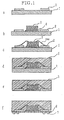
- a nickel layer of 0.001 mm in thickness (not shown in FIG. 1) was plated on one side of an electrolytic copper foil 1 of 0.035 mm in thickness.
- a photosensitive dry film resist (“PHOTEC HN340", trade name; product of Hitachi Chemical Co., Ltd.) was laminated, exposed and then developed, so that a plating resist for wiring pattern was formed.
- electrolytic copper plating was conducted in a copper sulfate bath. Applied further were a nickel plating to a thickness of 0.003 mm or greater and a gold plating of 99.9% or higher purity to a thickness of 0.0003 mm or greater.
- the plating resist was next stripped off, whereby a wiring 2 was formed (FIG. 1a).
- an LSI chip 3 was mounted (FIG. 1b).
- a silver paste 4 for semiconductors was used for bonding the LSI chip.
- LSI terminals and the wiring 2 was connected by wire bonds 100 (FIG. 1c).
- the thus-formed assembly was loaded in a die for transfer mold and sealed with a semiconductor-sealing epoxy resin ("CL-7700", trade name; product of Hitachi Chemical Co., Ltd.) 5 (FIG. 1d). Thereafter, only the copper foil 1 was dissolved away with an alkali etchant to expose the nickel. The nickel layer was removed with a nickel stripper having low copper-dissolving power so that the wiring portions were exposed (FIG. 1e).
- solder resist 6 was coated and patterned in such a way that connecting terminal portions were exposed.
- Solder balls 7 were arranged at the exposed portions of the wiring and were caused to fuse there (FIG. 1f). The wiring could be connected to an outer wiring via these solder balls 7.
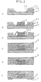
- a copper foil 1 with a wiring 2 was prepared (FIG. 2a).
- An LSI chip 3 was mounted.
- the LSI chip was provided with gold bumps 8 at terminal portions. These gold bumps 8 and terminal portions of the wiring 2 were connected together by thermocompression (FIG. 2b).
- a liquid epoxy resin 9 was filled underneath the LSI chip and cured (FIG. 2c).
- the thus-formed assembly was loaded in a die for transfer mold and sealed with a semiconductor-sealing epoxy resin ("CL-7700", trade name; product of Hitachi Chemical Co., Ltd.) 10 (FIG. 2d). Thereafter, only the copper foil 1 was dissolved away with an alkali etchant to expose the nickel.
- the nickel layer was removed with a nickel stripper having low copper-dissolving power so that the wiring portions were exposed (FIG. 2e). Then, a solder resist 6 was coated and patterned in such a way that connecting terminal portions were exposed. Solder balls 7 were arranged at the exposed portions of the wiring and were caused to fuse there (FIG. 2f). The wiring could be connected to an outer wiring via these solder balls 7.
- a nickel layer of 0.001 mm in thickness (not shown in FIG. 3) was plated on one side of an electrolytic copper foil 1 of 0.035 mm in thickness.
- a photosensitive dry film resist (“PHOTEC HN340", trade name; product of Hitachi Chemical Co., Ltd.) was laminated, exposed and then developed, so that a plating resist for wiring pattern was formed.
- electrolytic copper plating was conducted in a copper sulfate bath, so that a first wiring 13 was formed.
- the plating resist was next stripped off and the first wiring 13 was subjected at a surface thereof to oxidation treatment and reduction treatment.
- the terminal portions was applied with a nickel plating to a thickness of 0.003 mm or greater and further with a gold plating of 99.9% or higher purity to a thickness of 0.0003 mm or greater (FIG. 3a).
- an LSI chip was mounted on the copper foil 1 with the two-layer wiring pattern formed thereon as described above.
- a silver paste for semiconductors was used (FIG. 3b).
- LSI terminals and the wiring 13 were connected by wire bonds 100 (FIG. 3c).
- the thus-formed assembly was loaded in a die for transfer mold and sealed with a semiconductor-sealing epoxy resin ("CL-7700", trade name; product of Hitachi Chemical Co., Ltd.) 5.
- solder resist 6 was coated and patterned in such a way that connecting terminal portions were exposed. Solder balls 7 were arranged at the exposed portions and were caused to fuse there (FIG. 3f). The wiring could be connected to an outer wiring via these solder balls 7.
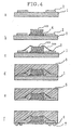
- a photosensitive dry film resist ("PHOTEC HN340", trade name; product of Hitachi Chemical Co., Ltd.) was laminated, exposed and then developed, so that a plating resist for wiring pattern was formed. Subsequently, electrolytic copper plating was conducted in a copper sulfate bath. Applied further were a nickel plating to a thickness of 0.003 mm or greater and a gold plating of 99.9% or higher purity to a thickness of 0.0003 mm or greater. The plating resist was next stripped off, whereby a wiring 2 was formed (FIG. 4a).
- a semiconductor chip 103 was mounted (FIG. 4b).
- a silver paste 4 for semiconductors was used for bonding the semiconductor chip.
- semiconductor terminals and the wiring 2 were connected by wire bonds 100 (FIG. 4c).
- the thus-formed assembly was loaded in a die for transfer mold and sealed with a semiconductor-sealing epoxy resin ("CL-7700", trade name; product of Hitachi Chemical Co., Ltd.) 5 (FIG. 4d).
- the SUS sheet 14 was mechanically stripped off to expose the wiring portion (FIG. 4e).
- a solder resist 6 was coated and patterned in such a way that connecting terminal portions were exposed.
- Solder balls 7 were arranged at the exposed portions of the wiring and were caused to fuse there (FIG. 4f).
- the wiring could be connected to an outer wiring via these solder balls 7.
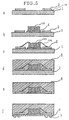
- a photosensitive dry film resist ("PHOTEC HN340", trade name; product of Hitachi Chemical Co., Ltd.) was laminated, exposed and then developed, so that a plating resist for wiring pattern was formed.
- electrolytic copper plating is conducted in a copper sulfate bath.
- a nickel plating to a thickness of 0.003 mm or greater and a gold plating of 99.9% or higher purity to a thickness of 0.0003 mm or greater.
- the plating resist was next stripped off, whereby a wiring 2 was formed (FIG. 5a).
- a semiconductor chip 103 was mounted (FIG. 5b).
- a silver paste 4 for semiconductors was used for bonding the semiconductor chip.
- semiconductor terminal portions and the wiring 2 were connected by wire bonds 100 (FIG. 5c).
- the thus-formed assembly was loaded in a die for transfer mold and sealed with a semiconductor-sealing epoxy resin ("CL-7700", trade name; product of Hitachi Chemical Co., Ltd.) 5 (FIG. 5d).
- the copper foil 1 was dissolved away with an alkali etchant to expose the wiring portions of nickel (FIG. Se).
- a solder resist 6 was coated and patterned in such a way that connecting terminal portions were exposed.
- Solder balls 7 were arranged at the exposed portions of the wiring and were caused to fuse there (FIG. 5f).
- the wiring could be connected to an outer wiring via these solder balls 7.
- a photosensitive dry film resist ("PHOTEC HN340", trade name; product of Hitachi Chemical Co., Ltd.) was laminated, exposed and then developed, so that a plating resist for wiring pattern was formed. Applied further were a gold plating of 99.9% or higher purity to a thickness of 0.0003 mm or greater and a nickel plating to a thickness of 0.003 mm or greater. Further, electrolytic copper plating was conducted in a copper sulfate bath, and the plating resist was stripped off, whereby a wiring 2 is formed (FIG. 6a).
- a polyimide film 16 was bonded, connecting terminal portions of the wiring 2 were exposed by a laser (FIG. 6b), and the copper foil 1 was etched off (FIG. 6c).
- a photosensitive film in place of the polyimide film 16 made it possible to expose connecting terminal portions without using a laser.
- an LSI chip 3 was mounted on the surface of the polyimide film 16 on which the wiring pattern was formed.
- a silver paste 4 for semiconductors was used for bonding the LSI chip.
- semiconductor terminal portions and the wiring 2 were connected by wire bonds 100 (FIG. 6d).
- the thus-formed assembly was loaded in a die for transfer mold and sealed with a semiconductor-sealing epoxy resin ("CL-7700", trade name; product of Hitachi Chemical Co., Ltd.) 5 (FIG. 6e). Thereafter, solder balls 7 were arranged at the connecting terminal portions and are caused to fuse there (FIG. 6f). The wiring could be connected to an outer wiring via these solder balls 7.
- CL-7700 semiconductor-sealing epoxy resin
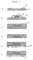
- a nickel layer of 0.001 mm in thickness (not shown in FIG. 7) was plated on one side of an electrolytic copper foil 1 of 0.035 mm in thickness.
- a photosensitive dry film resist (“PHOTEC HN340", trade name; product of Hitachi Chemical Co., Ltd.) was laminated, exposed and then developed, so that a plating resist for wiring pattern was formed.
- electrolytic copper plating was conducted in a copper sulfate bath. Applied further were a nickel plating to a thickness of 0.003 mm or greater and a gold plating of 99.9% or higher purity to a thickness of 0.0003 mm or greater.
- the plating resist was next stripped off, whereby a wiring 2 was formed (FIG. 7a).
- an LSI chip 3 was mounted on the copper foil 1 with the wiring 2 formed thereon as described above.
- a silver paste 4 for semiconductors was used for bonding the LSI chip.
- semiconductor terminal portions and the wiring 2 were connected by wire bonds 100 (FIG. 7b).
- the thus-formed assembly was loaded in a die for transfer mold and sealed with a semiconductor-sealing epoxy resin ("CL-7700", trade name; product of Hitachi Chemical Co., Ltd.) 5 (FIG. 7c). Thereafter, only the copper foil 1 was dissolved away with an alkali etchant to expose the nickel. The nickel layer was removed with a nickel stripper having low copper-dissolving power so that the wiring portion was exposed (FIG. 7d).
- solder balls 7 were arranged at the exposed portions of the wiring and are caused to fuse there (FIG. 7f). The wiring can be connected to an outer wiring via these solder balls 7.
- a photosensitive dry film resist ("PHOTEC HN340", trade name; product of Hitachi Chemical Co., Ltd.) was laminated, exposed and then developed, so that a plating resist for wiring pattern was formed. Applied further were a gold plating of 99.9% or higher purity to a thickness of 0.0003 mm or greater and a nickel plating to a thickness of 0.003 mm or greater. Further, electrolytic copper plating was conducted in a copper sulfate bath, and the plating resist was stripped off, whereby a wiring 2 was formed (FIG. 8a).
- a liquid sealing resin 17 was coated by screen printing, and an insulating layer was formed in such a manner that connecting terminal portions of the wiring 2 were exposed (FIG. 8b).
- the copper foil 1 was etched off (FIG. 8c).
- an LSI chip 3 was mounted on the surface of the hardened liquid sealing resin 16 in which the wiring pattern exist.
- a silver paste 4 for semiconductors was used for bonding the LSI chip.
- semiconductor terminal portions and the wiring 2 were connected by wire bonds 100 (FIG. 8d).
- the thus-formed assembly was loaded in a die for transfer mold and sealed with a semiconductor-sealing epoxy resin ("CL-7700", trade name; product of Hitachi Chemical Co., Ltd.) 5 (FIG. 8e). Thereafter, solder balls 7 were arranged at the connecting terminal portions of the wiring 2 and were caused to fuse there (FIG. 8f). The wiring could be connected to an outer wiring via these solder balls 7.
- CL-7700 semiconductor-sealing epoxy resin
- a nickel layer of 0.001 mm in thickness (not shown in FIG. 9) was plated on one side of an electrolytic copper foil 1 of 0.035 mm in thickness.
- a photosensitive dry film resist (“PHOTEC HN340", trade name; product of Hitachi Chemical Co., Ltd.) was laminated, exposed and then developed, so that a plating resist for wiring pattern was formed.
- electrolytic copper plating was conducted in a copper sulfate bath. Applied further were a nickel plating to a thickness of 0.003 mm or greater and a gold plating of 99.9% or higher purity to a thickness of 0.0003 mm or greater.
- the plating resist is next stripped off, whereby a wiring 2 is formed (FIG. 9a).
- an LSI chip 3 is mounted on the copper foil 1 with the wiring 2 formed thereon as described above.
- a silver paste 4 for semiconductors was used for bonding the LSI chip 3.
- semiconductor terminals and the wiring 2 were connected by wire bonds 100 (FIG. 9b).
- the thus-formed assembly was loaded in a die for transfer mold and sealed with a semiconductor-sealing epoxy resin ("CL-7700", trade name; product of Hitachi Chemical Co., Ltd.) 5 (FIG. 9c). Thereafter, only the copper foil 1 was dissolved away with an alkali etchant to expose the nickel. The nickel layer was removed with a nickel stripper having low copper-dissolving power so that the wiring portion was exposed (FIG. 9d).
- a nickel layer of 0.001 mm in thickness (not shown in FIG. 10) was plated on one side of an electrolytic copper foil 1 of 0.035 mm in thickness.
- a photosensitive dry film resist (“PHOTEC HN340", trade name; product of Hitachi Chemical Co., Ltd.) was laminated, exposed and then developed, so that a plating resist for a wiring pattern and registration marks was formed.
- electrolytic copper plating is conducted in a copper sulfate bath. Applied further are a nickel plating to a thickness of 0.003 mm or greater and a gold plating of 99.9% or higher purity to a thickness of 0.0003 mm or greater.
- the plating resist was next stripped off, whereby a wiring 2 and registration marks 18 were formed (FIG. 10a). Only portions with the registration marks 18 formed thereon were held between SUS sheets and then pressed, whereby the registration marks were caused to appear on the back side of the copper foil 1 as if they were die-stamped (FIG. 10b). On the copper foil 1 with the wiring 2 and the registration mark 18 formed thereon as described above, an LSI chip 3 was mounted (FIG. 10c). For bonding the LSI chip 3, a silver paste 4 for semiconductors was used. Next, semiconductor terminals and the wiring 2 were connected by wire bonds 100 (FIG. 10d).
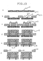
- a photosensitive dry film resist ("PHOTEC HN340", trade name; product of Hitachi Chemical Co., Ltd.) was laminated, exposed and then developed, so that a plating resist for plural sets of wiring patterns was formed. Applied further were a gold plating of 99.9% or higher purity to a thickness of 0.0003 mm or greater and a nickel plating to a thickness of 0.003 mm or greater. Further, electrolytic copper plating was conducted in a copper sulfate bath, and the plating resist was stripped off, whereby plural sets of wiring 2 were formed (FIG. 11a).
- the thus-formed assembly was loaded in a die for transfer mold and sealed with a semiconductor-sealing epoxy resin ("CL-7700", trade name; product of Hitachi Chemical Co., Ltd.) 5 (FIG. 11e). Thereafter, solder balls 7 were arranged at the connecting terminal portions of the wiring 2 and were caused to fuse there (FIG. 11f). The wiring could be connected to outer wiring via these solder balls 7, respectively. Finally, the packages connected together with the polyimide film were punched out by dies (FIG. 11g).
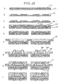
- FIG. 12a An adhesive-coated polyimide film 20 of 0.07 mm in thickness was punched by dies to form openings at portions where connecting terminals were to be formed (FIG. 12a).
- a copper foil 21 of 0.035 mm in thickness (FIG. 12b)
- a photosensitive dry film resist (“PHOTEC HN340", trade name; product of Hitachi Chemical Co., Ltd.)waslaminated, exposed and then developed, so that an etching resist for plural sets of wiring patterns was formed.
- the copper foil wasetched and the resist was stripped off, then plural sets of wiring patterns 2 was formed (FIG. 12c). After the plural sets of wiring patterns were formed on the single polyimide film as described above, LSI chips 3 were mounted.
- die-bonding tapes 4' for semiconductors were used for bonding the LSI chips 3.
- semiconductor terminal portions and the wiring 2 were connected by wire bonds 100 (FIG. 12d).
- the thus-formed assembly was loaded in a die for transfer mold and sealed with a semiconductor-sealing epoxy resin ("CL-7700", trade name; product of Hitachi Chemical Co., Ltd.) 5 (FIG. 12e).
- solder balls 7 were arranged at the connecting terminal portions of the wiring and were caused to fuse there (FIG. 12f).
- the wiring could be connected to outer wiring via these solder balls 7.
- the packages connected together with the polyimide film were punched out by dies (FIG. 12g).
- a nickel layer of 0.001 mm in thickness (not shown in FIG. 13) was plated on one side of an electrolytic copper foil 1 of 0.035 mm in thickness.
- a photosensitive dry film resist (“PHOTEC HN340", trade name; product of Hitachi Chemical Co., Ltd.) was laminated, exposed and then developed, so that a plating resist for plural sets of wiring patterns was formed.
- electrolytic copper plating was conducted in a copper sulfate bath. Applied further were a nickel plating to a thickness of 0.003 mm or greater and a gold plating of 99.9% or higher purity to a thickness of 0.0003 mm or greater. The plating resist was stripped off, whereby wiring 2 were formed (FIG. 13a).
- the copper foil 1 with the wiring 2 formed thereon were divided into individual units and bonded to a separately-prepared stainless steel frame 22 (thickness: 0.135 mm) via a polyimide adhesive film (FIG. 13b).
- a copper alloy such as phosphor bronze, a copper foil, a nickel foil, a nickel alloy foil or the like could also be used.
- inter alia bonding making use of an intermetallic eutectic reaction or bonding making use of an ultrasonic wave.
- FIG. 14 it is desired to inspect the wiring on the copper foil 1 beforehand, to select only connection non-defectives 23 and then to bond the thus-selected connection non-defectives to the frame 22.
- FIG. 14 there were shown the electrolytic copper foil 1, the frame 22, connection defectives 24, and registration holes 25. Although each cut-off copper foil was provided with one wiring in this embodiment, plural sets of wiring may be arranged on each cut-off copper foil. As a positional relationship between the frame 22 and each copper foil upon bonding them together, various positional relationships were feasible as shown by way of example in FIGS. 15(a) and 15(b).
- FIG. 15 shows the frame 22 in plan view, in which there were illustrated an opening 26 in the frame, a mounting position 27 for the copper foil with the wiring, and a foil-fixing adhesive 28.
- LSI chips 3 were mounted, and semiconductor terminal portions and their corresponding wiring 2 were connected by wire bonds 100 (FIG. 13c).
- die-bonding tapes 4' for semiconductors were used for mounting the LSI chips.
- die-bonding silver paste or the like could be used instead of the bonding tapes 4'.
- a conventional wire-bonding method was used for the mounting of semiconductor chips.
- Other methods such as Flip chips may also be used.
- the thus-formed assembly was loaded in a die for transfer mold and sealed with a semiconductor-sealing epoxy resin ("CL-7700", trade name; product of Hitachi Chemical Co., Ltd.) 5 (FIG. 13d). Thereafter, only the copper foil 1 was dissolved away with an alkali etchant to expose the nickel. The nickel layer was removed with a nickel stripper having low copper-dissolving power so that the wiring portions were exposed.
- CL-7700 semiconductor-sealing epoxy resin
- solder resist 6 was coated and patterned in such a way that connecting terminal portions were exposed.
- Solder balls 7 were arranged at the exposed portions of the wiring and were caused to fuse there (FIG. 13e).
- the thus-obtained assembly was cut apart by a cutter and unnecessary cut pieces 101 of the frame 22 were eliminated, so that the assembly was divided into individual semiconductor packages (FIG. 13f).
- Each wiring could be connected to an outer wiring via its corresponding solder balls 7.
- An adhesive-coated polyimide film 29 of 0.07 mm in thickness was punched by dies to form openings at portions where connecting terminal portions were to be formed.
- a photosensitive dry film resist (“PHOTEC HN340", trade name; product of Hitachi Chemical Co., Ltd.) was laminated, exposed and then developed, so that an etching resist for plural sets of wiring patterns was formed.
- the copper foil was etched and the resist was stripped off, whereby plural sets of wiring 2 were formed (FIG. 16a).
- the connecting terminal portions and the wiring 2 were be formed using a material which was formed of a copper foil and a polyimide coated directly on the copper foil (for example, "50001", trade name; product of Hitachi Chemical Co., Ltd.).
- the formation of the openings could be effected by drilling, laser beam machining such as excimer laser machining, printing or the like.
- they could also be formed by using a material, which has been obtained by imparting photosensitivity to a polyimide, and conducting exposure and development.
- the polyimide another material such as a sealing resin could also be used.
- the wiring-formed film was divided into units. They were then bonded to a separately-prepared stainless steel frame 22 (thickness: 0.135 mm) via a polyimide adhesive 28 (FIG. 16b). Then, LSI chips 3 were mounted, and semiconductor terminal portions and the corresponding wiring 2 were connected by wire bonds 100 (FIG. 16c). For the mounting of the LSI chips, die-bonding tapes 4' for semiconductors were used. The thus-formed assembly was loaded in a die for transfer mold and sealed with a semiconductor-sealing epoxy resin ("CL-7700", trade name; product of Hitachi Chemical Co., Ltd.) 5 (FIG. 16d).
- CL-7700 semiconductor-sealing epoxy resin
- solder balls 7 were arranged in the openings, which were formed in the beginning and were to be converted to connecting terminal portions, and were caused to fuse there (FIG. 16e).
- the wiring could be connected to outer wiring via these solder balls 7, respectively.
- the packages connected together with the frame were punched out by dies into individual packages (FIG. 16f).
- a two-layer flexible base material was composed of a metal foil 31 and an insulating base material 32 formed directly thereon (FIG. 17a).
- a predetermined resist pattern was formed on the metal foil.
- desired plural sets of wiring patterns 33 were formed, and the resist pattern was then stripped off (FIG. 17b).
- a composite metal foil which has a thin copper layer on a carrier foil removable in a subsequent step, or the like could also be used besides a single foil such as an electrolytic copper foil, a rolled copper foil or a copper alloy foil.
- a metal foil - which was obtained by forming a nickel-phosphorus plating layer of 0.2 ⁇ m or so in thickness on one side of an electrolytic copper foil of 18 ⁇ m in thickness and then plating a thin copper layer to a thickness of 5 ⁇ m or so - was applicable.
- the thin copper layer was exposed by etching off the copper foil and nickel-phosphorus layer subsequent to formation of a polyimide layer on the thin copper layer.
- the thin copper layer may be patterned after the thin copper layer was exposed in its entirety, or the carrier foil (copper foil/thin nickel layer) may be used as a part of a leadframe structure.
- a polyimide material is ordinary from the viewpoint of process heat resistance and the like.
- the polyimide a polyimide containing 70 mole % or more of a polyimide having repeating units represented by the following formula (1) because a marked warp would be developed in the base material in a solder reflowing step if the polyimide and the copper foil had different coefficients of thermal expansion:
- holes 34 reaching the copper foil were formed at positions which were to be converted to connecting portions to an external substrate in a subsequent step (FIG. 17c).
- No particular limitation was imposed on the method for the formation of the holes.
- a laser beam machining making use of an excimer laser, CO 2 laser or YAG laser, a wet etching process and so on is applicable.
- a frame base material 37 which was coated with an adhesive 36 and has been punched out at predetermined portions (openings 35) by punching or the like, was then bonded to surfaces of the wiring patterns (FIG. 17d).
- a polyimide film or a metal foil such as a copper foil is applicable. If the thickness of the polyimide layer of the two-layer flexible base material was 25 ⁇ m and the bonded frame base material is a polyimide film, a film thickness as much as 50 to 70 ⁇ m was required to assure sufficient rigidity for the whole frame.
- no particular limitation was imposed on the area where the frame base material layer was formed.
- the frame base material layer in areas where semiconductor chips were to be mounted. Specifically, where the mounting of chips was effected by the wire-bonding method, the frame base material layer may be arranged in the entire area insofar as at least terminal portions 38 were exposed for wire-bonding. Semiconductor chips 39 were then mounted, and the semiconductor chips and the wiring patterns were electrically connected together by gold wires 40 (FIG. 17e). Where a face-down method was adopted as a mounting method for semiconductor chips, on the other hand, the wiring patterns were provided with metal bumps or the like at predetermined positions (which correspond to the positions of external connection electrodes of the semiconductor chips), and the semiconductor chips and the wiring patterns may be electrically connected together via the metal bumps.
- the thus-obtained assembly was then loaded in a die for transfer mold and was sealed with a resinous sealing material 41 (FIG. 17f).
- a resinous sealing material 41 (FIG. 17f).
- As a method for the formation of the connecting portions 42 it was possible to apply a method such that bumps were formed beforehand to a thickness greater than the polyimide film by an electrolytic plating process after the step of FIG. 17c or solder bumps were formed by a solder printing process after sealing with the resin.
- the package portions were cut off from the frame so that packages were obtained as desired (FIG. 17g).
- a two-layer flexible base material having an electrolytic copper foil of 12 ⁇ m in thickness on one side thereof (“MCF 5000I", trade name; product of Hitachi Chemical Co., Ltd.) was provided.
- a dry film resist (“PHOTEC HK815", trade name; product of Hitachi Chemical Co., Ltd.) was laminated on the copper foil and then exposed and developed, whereby a desired resist pattern was obtained. After the copper foil was etched with a solution of ferric chloride, the resist pattern was stripped with a solution of potassium hydroxide so that a predetermined wiring pattern was obtained.
- an excimer laser beam machine (“INDEX 200", trade name; manufactured by Sumitomo Heavy Industries, Ltd.), as many holes as needed (diameter: 300 ⁇ m) were formed at predetermined positions so that they extend from a side of an insulating base material and reach a back surface of the wiring pattern.
- the following conditions were set for the excimer laser beam machining - energy density: 250 mJ/cm 2 , reduction ratio: 3.0, oscillation frequency: 200 Hz, and illumination pulse number: 300 pulses.
- thermocompression bonding a 10- ⁇ m thick polyimide-base adhesive ("AS 2250", trade name; product of Hitachi Chemical Co., Ltd.) on one side of a 50- ⁇ m thick polyimide film ("UPILEX S”, trade name; product of Ube Industries, Ltd.).
- Predetermined areas including those corresponding to terminal portions to be used for wire bonding in a subsequent step were removed by punching, and the polyimide film and the two-layer flexible base material with the wiring pattern formed thereon were subjected to thermocompression via the adhesive.
- the following conditions were set for the thermo compression bonding - pressure: 20 kgf/cm 2 , temperature: 180°C, and thermocompression time: 60 minutes.
- the terminal portions for the wire bonding were next applied with nickel/gold platings.
- the thicknesses of these platings were 3 ⁇ m and 0.3 ⁇ m, respectively.
- semiconductor-chip-mounting die-bonding material (“HM-1", trade name; product of Hitachi Chemical Co., Ltd.)
- HM-1 semiconductor-chip-mounting die-bonding material
- the mounting conditions were set as follows - press pressure: 5 kgf/cm 2 , bonding temperature: 380°C, and compression-bonding time: 5 seconds. External electrode portions of each semiconductor chip were then electrically connected with its corresponding wiring pattern by wire bonding.
- the thus-obtained assembly was stamped into a leadframe-shaped form, loaded in a die for transfer mold and then sealed at 185°C for 90 seconds with a semiconductor-sealing epoxy resin ("CL-7700", trade name; product of Hitachi Chemical Co., Ltd.).
- CL-7700 semiconductor-sealing epoxy resin
- the above-mentioned holes were then each coated with a predetermined amount of solder by a printing process.
- the solder was caused to fuse in an infrared reflowing oven, so that external connection bumps were formed.
- the package portions were punched out by dies so that packages were obtained as desired.
- a two-layer flexible base material was composed of a metal foil 31 and an insulating base material 32 formed directly thereon (FIG. 18a).
- a predetermined resist pattern was formed on the metal foil.
- desired plural sets of wiring patterns 33 were formed, and the resist pattern was then stripped off (FIG. 18b).
- a composite metal foil which had a thin copper layer on a carrier foil removable in a subsequent step, or the like could also be used besides a single foil such as an electrolytic copper foil, a rolled copper foil or a copper alloy foil.
- a metal foil - which was obtained by forming a nickel-phosphorus plating layer of 0.2 ⁇ m or so in thickness on one side of an electrolytic copper foil of 18 ⁇ m in thickness and then plating a thin copper layer to a thickness of 5 ⁇ m or so - was applicable.
- the thin copper layer was exposed by etching off the copper foil and nickel-phosphorus layer subsequent to formation of a polyimide layer on the thin copper layer.
- the thin copper layer might be patterned after the thin copper layer was exposed in its entirety, or the carrier foil (copper foil/thin nickel layer) might be used as a part of a leadframe structure.
- a polyimide material was ordinary from the viewpoint of process heat resistance and the like.
- the polyimide a polyimide containing 70 mole % or more of a polyimide having repeating units represented by the formula (1) because a marked warp would be developed in the base material in a solder reflowing step if the polyimide and the copper foil had different coefficients of thermal expansion.
- holes 34 reaching the copper foil were formed at positions which were to be converted to connecting portions to external substrate in a subsequent step (FIG. 18c).
- No particular limitation was imposed on the method for the formation of the holes.
- a wet etching process or the like was applicable.
- a frame base material 37 which was coated with an adhesive 36 and had been punched out at predetermined portions (openings 35) by punching or the like, is then bonded as a second insulating base material to surfaces of the wiring patterns (FIG. 18d).
- the thickness of the polyimide layer of the two-layer flexible base material is 25 ⁇ m, a film thickness as much as 50 to 70 ⁇ m was required as a thickness of a polyimide film to be bonded in view of a subsequent step in which the polyimide film is fixed on a frame.
- no particular limitation was imposed on the area where the polyimide was bonded. Its arrangement in areas where semiconductor chips were to be mounted made it possible to form external connection terminals under the semiconductor chips like CSPs.
- the polyimide film might be bonded in the entire area insofar as at least terminal portions 38 were exposed for wire-bonding.
- the insulating substrate obtained as described above was divided into the individual wiring patterns (FIG. 18e) and were then fixed on a separately-prepared frame 43 made, for example, of SUS or the like (FIG. 18f).
- Semiconductor chips 39 were then mounted, and the semiconductor chips and the wiring patterns were electrically connected together by gold wires 40 (FIG. 18g).
- the wiring patterns were provided with metal bumps or the like at predetermined positions (which correspond to the positions of external connection electrodes of the semiconductor chips), and the semiconductor chips and the wiring patterns might be electrically connected together via the metal bumps.
- the thus-obtained assembly was then loaded in a die for transfer mold and was sealed with a resinous sealing material 41 (FIG. 18h).
- a resinous sealing material 41 (FIG. 18h).
- an epoxy resin containing 5 to 80 wt.% of silica of about 10 to 20 ⁇ m in diameter could be used.
- the connecting portions 42 As a method for the formation of the connecting portions 42 it was possible to apply a method such that bumps were formed beforehand to a thickness greater than the polyimide film by an electrolytic plating process after the step of FIG. 18c or solder bumps were formed by a solder printing process after sealing with the resin. Finally, the package portions were cut off from the frame so that packages were obtained as desired (FIG. 18i).
- FIG. 18 The sixteenth embodiment of FIG. 18 will be described more specifically.
- a two-layer flexible base material having an electrolytic copper foil of 12 ⁇ m in thickness on one side thereof (“MCF 5000I", trade name; product of Hitachi Chemical Co., Ltd.) was provided.
- a dry film resist (“PHOTEC HK815", trade name; product of Hitachi Chemical Co., Ltd.) was laminated on the copper foil and then exposed and developed, whereby a desired resist pattern was obtained. After the copper foil was etched with a solution of ferric chloride, the resist pattern was stripped with a solution of potassium hydroxide so that a predetermined wiring pattern was obtained.
- an excimer laser beam machine (“INDEX 200", trade name; manufactured by Sumitomo Heavy Industries, Ltd.), as many holes as needed (diameter: 300 ⁇ m) were formed as many as needed at predetermined positions so that they extend from a side of an insulating base material and reach a back surface of the wiring pattern.
- the following conditions were set for the excimer laser beam machining - energy density: 250 mJ/cm 2 , reduction ratio: 3.0, oscillation frequency: 200 Hz, and illumination pulse number: 300 pulses.
- thermocompression bonding a 10- ⁇ m thick polyimide-base adhesive ("AS 2250", trade name; product of Hitachi Chemical Co., Ltd.) on one side of a 50- ⁇ m thick polyimide film ("UPILEX S”, trade name; product of Ube Industries, Ltd.).
- Predetermined areas including those corresponding to terminal portions to be used for wire bonding in a subsequent step were removed by punching, and the polyimide film and the two-layer flexible base material with the wiring pattern formed thereon were subjected to thermocompression via the adhesive.
- the following conditions were set for the thermo compression bonding - pressure: 20 kgf/cm 2 , temperature: 180°C, and thermocompression time: 60 minutes.
- the terminal portions for the wire bonding were next applied with nickel/gold platings.
- the thicknesses of these platings were 3 ⁇ m and 0.3 ⁇ m, respectively.
- the thus-obtained substrate was divided into the individual wiring patterns and are fixed on a separately-prepared SUS frame.
- semiconductor-chip-mounting die-bonding material ("HM-1", trade name; product of Hitachi Chemical Co., Ltd.)
- semiconductor chips were then mounted.
- the mounting conditions were set as follows - press pressure: 5 kgf/cm 2 , bonding temperature: 380°C, and compression-bonding time: 5 seconds.
- External electrode portions of each semiconductor chip were then electrically connected with its corresponding wiring pattern by wire bonding.
- the thus-obtained assembly was molded into a lead frame-shaped form, loaded in a die for transfer mold and then sealed at 185°C for 90 seconds with a semiconductor-sealing epoxy resin ("CL-7700", trade name; product of Hitachi Chemical Co., Ltd.).
- CL-7700 semiconductor-sealing epoxy resin
- the above-mentioned holes were then each coated with a predetermined amount of solder by a printing process.
- the solder was caused to fuse in an infrared reflowing oven, so that external connection bumps were formed.
- the package portions were punched out by dies so that packages were obtained as desired.
- Plural sets of predetermined wiring patterns 52 were formed on a supporting member 51 (FIG. 19a).
- an insulating base material such as a polyimide film could be used besides a metal foil such as an electrolytic copper foil.
- an insulating base material there were two methods. According to the first method, nonthrough-holes reaching the wiring patterns were formed at predetermined positions of the insulating base material, and external connection terminals were formed at exposed portions of the wiring patterns. The nonthrough-holes could be formed by applying an excimer laser or a CO 2 laser and so on. According to the second method, a drilled insulating base material provided with an adhesive was formed in advance and, subsequent to lamination with an electrolytic copper foil or the like, the copper foil was subjected to etching.
- a resist pattern was formed with a photoresist and wiring patterns were then formed by electroplating while using the metal foil as a cathode.
- FIG. 20 shows grooves 59 formed in boundary portions between individual package portions. The width, depth and the like of each groove could be modified depending on the dimensions which the die for transfer mold could receive for processing.
- FIG. 21 illustrates a transfer molding process which was carried out using a grid-shaped intermediate plate 60 hollowed out beforehand at areas corresponding to the individual package portions.
- the supporting member was a metal foil
- the supporting member was removed by a chemical etching process and external connection terminals 57 were formed at predetermined positions (FIG. 19d).
- an insulating base material was used as a supporting member, it was only necessary to selectively remove the insulating base material at predetermined areas by a laser or the like.
- the substrate which had been sealed as a whole is cut apart into unit portions 58.
- a solder resist layer might be formed on exposed surfaces of the wiring patterns for protecting the wiring patterns.
- the resultant assembly was dried at 85°C for 15 minutes and then cut into the individual blocks.
- semiconductor-device-mounting die-bonding material ("HM-1", trade name; product of Hitachi Chemical Co., Ltd.)
- HM-1 semiconductor-device-mounting die-bonding material
- the bonding conditions were set as follows - press pressure: 5 kgf/cm 2 , temperature: 380°C, and compression-bonding time: 5 seconds.
- External terminals of each semiconductor device were then electrically connected with its corresponding gold-plated terminal portions (second connecting portions) by wire bonding.
- the thus-obtained assembly was loaded in a die for transfer mold.
- the 75 wiring patterns (corresponding to 1 block) were sealed all together at 185°C for 90 seconds so that the individual wiring patterns were transferred into the sealing material.
- the electrolytic copper foil was etched off at desired portions with an alkali etchant ("A Process", trade name; product of Japan Meltex, Inc.).
- the temperature and spraying pressure of the etching solution were 40°C and 1.2 kgf/cm 2 , respectively.
- Solder patterns were then formed at external connection terminal portions by a printing process. The solder was caused to fuse in an infrared reflowing oven, so that external connection bumps were formed. Finally, the assembly was divided into individual package portions by a diamond cutter so that packages were obtained as desired.
- the resultant assembly was dried at 85°C for 15 minutes and then cut into the individual blocks.
- a semiconductor-device-mounting die-bonding material ("HM-1", trade name; product of Hitachi Chemical Co., Ltd.)
- the semiconductor devices were then bonded.
- the bonding conditions were set as follows - press pressure: 5 kgf/cm 2 , temperature: 380°C, and compression-bonding time: 5 seconds.
- External terminals of each semiconductor device were then electrically connected with its corresponding gold-plated terminal portions (second connecting portions) by wire bonding.
- Using as an intermediate plate a grid-shaped stainless steel plate hollowed out at areas corresponding to individual package areas, the thus-obtained assembly was loaded in a die for transfer mold.
- the 75 wiring patterns (corresponding to 1 block) were sealed all together at 185°C for 90 seconds so that the individual wiring patterns were transferred into the sealing material.
- a grid portion of the intermediate plate was tapered at 12° to facilitate separation of the individual packages from the intermediate plate.
- the electrolytic copper foil was etched off at desired portions with an alkali etchant ("A Process", trade name; product of Japan Meltex, Inc.). Each package portion was held in place by the grid-shaped intermediate plate.
- the temperature and spraying pressure of the etching solution were 40°C and 1.2 kgf/cm 2 , respectively.
- solder patterns were formed at external connection terminal portions by a printing process. The solder was caused to fuse in an infrared reflowing oven, so that external connection bumps were formed. Individual package portions were separated from the intermediate plate so that packages were obtained as desired.
- Plural sets of predetermined resist patterns 62 (FIG. 22b) were formed on an electrically-conductive temporary supporting member 61 (FIG. 22a).
- wiring patterns 63 are formed at exposed portions of the temporary supporting member by an electroplating process.
- the temporary supporting member it was possible to use a conventional electrolytic copper foil and a foil consisting of an electrolytic copper foil and a thin layer of a metal (nickel, gold, solder or the like) different in chemical etching conditions from the copper foil provided thereon. Further, copper was preferred for the wiring patterns.
- the present invention was not limited to cases making use of a face-up method as a mounting method for semiconductor devices but was also applicable to cases making use of a face-down method for example. Specifically, it was only necessary to form bumps for face-down bonding at predetermined positions on the wiring patterns 63 by a plating process or the like and then to electrically connect external connecting portions of the semiconductor devices with the bumps.
- predetermined metal patterns 69 are formed at positions corresponding to the external connection terminals (FIG. 22f).
- any metal could be used insofar as it was not etched under conditions for etching off the electrically-conductive temporary supporting member.
- solder, gold, nickel/gold or the like could be used.
- a known electroplating process or solder printing process could be applied.
- solder bumps 70 could be formed by reflowing. In this case, by adjusting the thickness of the patterns 69, it was possible to control the height of the reflowed solder bumps 70.
- the temporary supporting member was next removed at predetermined portions while using the metal patterns as an etching resist, whereby the wiring patterns were exposed.
- the assembly was divided into individual packages 71 by stamping or dicing (FIG. 22g).
- the exposed wiring patterns were not protected by a corrosion-resistant metal such as nickel, areas other than the external connection terminal portions might be coated with a known solder resist or the like.
- solder as metal patterns, no particular limitation is imposed on the reflowing step.
- the reflowing step could be performed either before or after dividing the assembly into the individual packages.
- the reflowing step could also be conducted before mounting the individual packages on external wiring boards.
- the eighteenth embodiment will be described specifically.
- Wiring patterns which were each consisted of 0.2 ⁇ m thick nickel, 30 ⁇ m thick copper, 5 ⁇ m thick nickel and 1 ⁇ m thick soft gold were next formed by an electroplating method. The resist pattern was next stripped off using a 3 wt.% solution of potassium hydroxide of 35°C.
- the electroplated copper foil was etched off at desired portions with an alkali etchant ("A Process", trade name; product of Japan Meltex, Inc.).
- the temperature and spraying pressure of the etching solution were 40°C and 1.2 kgf/cm 2 , respectively.
- the solder was caused to fuse in an infrared reflowing oven, so that external connection bumps were formed.
- FIG. 23 The construction of a semiconductor mounting frame will be described with reference to FIG. 23.
- Numeral 89 indicated semiconductor-mounting substrates, each of which consisted of an insulating base material and wiring. Plural substrates were connected together via connecting portions 90.
- Each connecting portion 90 was provided with pinholes 91 as reference positions. Recognition marks employed in image recognition might be used in place of the pinholes 91. Based on these reference positions, positioning was performed in subsequent steps. Especially upon molding semiconductors with resin, positional registration was effected by inserting pins, which were arranged inside a cavity, in the pinholes 91.
- a nickel layer of 0.001 mm in thickness (not shown in FIGS. 24 and 25) was formed by an electrolytic plating process on one side of an electrolytic copper foil 81 of about 0.070 mm in thickness which was an electrically-conductive temporary substrate.
- a photosensitive dry film resist (“PHOTEC-HN340", trade name; product of Hitachi Chemical Co., Ltd.) was laminated, followed by exposure and development so that a plating resist for plural sets of wiring patterns was formed.
- the intensity of the exposure at this time is 70 mJ/cm 2 .
- FIG. 24a electrolytic copper plating was conducted in a known copper sulfate bath and the resist is stripped off, whereby plural sets of wiring 82 were formed (FIG. 24a, FIG. 25a).
- FIG. 25a it might be contemplated to form plated copper 82' at the connecting portions too. This makes it possible to provide the resulting frame with still enhanced rigidity.
- FIG. 24a and FIG. 25a could also be obtained by providing beforehand a base material composed of three layers of copper/thin nickel layer/copper and forming one of the copper foils into wiring in a usual etching step.
- the construction of the copper foil 81/thin nickel layer (not shown)/copper wirings 82 (and 82') obtained here might be replaced by a two-layer structure free of the thin nickel layer, such as copper foil/nickel wirings, nickel foil/copper wirings, or the like.
- the selectable kinds of metals were not limited to those of the present embodiment, it was a preferred standard for the selection to allow wirings to selectively remain when some parts of the temporary substrate were etched off in a subsequent step (FIG. 24c, FIG. 25c).
- the electrically-conductive temporary substrate became a material which made up the connecting portions of the frame, a greater thickness was preferred. There was however a subsequent step to etch it off partly, so that it was necessary to select an appropriate thickness.
- the thickness of the electrically-conductive temporary substrate varies depending on the material. For example, when a copper foil was used, about 0.03 to 0.3 mm or so was preferred.
- a polyimide adhesive 83 was next applied to the wiring-containing surface of the copper foil 81 with the plural sets of wiring 82 formed thereon.
- the polyimide adhesive 83 was not limited to this material. It was possible to use, for example, an epoxy adhesive film, a film formed of a polyimide film and an adhesive coated thereon, or the like.
- holes 84 for the external connection terminals were formed using an excimer laser (FIG. 24b, FIG. 25b). For the sake of simplification of subsequent steps, it was suited to arrange connecting terminals before mounting semiconductors.
- these holes 84 As another method for the formation of these holes 84, it was possible to form beforehand the holes 84 for the external connection terminals in a film by drilling or punching and then to bond the film so formed. Although no problem or inconvenience would arise even if a metal to be employed as the connecting terminals (which was designated at numeral 88 in FIG. 24f and FIG. 25f), such as a solder or the like, was filled at this stage, the resulting metal bumps may become an obstacle in the subsequent semiconductor mounting step and resin sealing step. Thus, it was preferred to form a metal at a subsequent step. It is preferred to locate the holes for the external connection terminals (or terminals) in the mounting substrate portions for the semiconductor devices, in the form of arrays on the side opposite to the side on which the semiconductor devices were mounted.
- etching solution As this etching solution, it was preferred to choose an etching solution and etching conditions, which in the case of this embodiment, provide a substantially higher dissolution velocity for copper than for nickel.
- an alkali etchant ("A Process", trade name; product of Japan Meltex Inc.) as an etching solution and, for example, a solution temperature of 40°C and a spray pressure of 1.2 kgf/cm 2 . It was to be noted that the kind of solution and the conditions specified here are merely illustrative.
- etching solution and etching conditions so that a substantially higher dissolution velocity was provided for nickel than for copper.
- selective etching was conducted with a nickel etchant ("Melstrip N950", trade name; product of Japan Meltex, Inc.).
- the temperature and spraying pressure of the etching solution were set at 40°C and 1.2 kgf/cm 2 , respectively. It was to be noted that the kind of the solution and conditions specified here were merely illustrative.
- the temporary substrate was allowed to remain as the connecting portions, whereby a semiconductor mounting frame having rigidity was obtained (FIG. 24c, FIG. 25c).
- electroless nickel-gold plating was applied to terminal portions of the copper wirings on this frame (not shown). This is needed for wire-bonding chips in a subsequent step. Such surface treatment could be applied as needed.
- semiconductor chips 85 were then mounted.
- semiconductor die-bonding tapes 86 for example, "HM-1", trade name; product of Hitachi Chemical Co., Ltd.
- the chips might be bonded using a die-bonding silver paste.
- terminal portions of the semiconductors and the wiring were connected by wire bonds 100 (FIG. 24d, FIG. 25d).
- the connection with the terminals of the semiconductors could be effected by another method, for example, by face-down connection making use of Flip chips or by bonding making use of an anisotropic conductive adhesive.
- the assembly so formed was loaded in a die for transfer mold and was sealed using a semiconductor-sealing epoxy resin ("CL-7700", trade name; product of Hitachi Chemical Co., Ltd.) 87 (FIG. 24e, FIG. 25e). Thereafter, solder balls 88 were arranged in the connecting holes formed at connecting terminal portions of the wiring 82 and were then caused to fuse (FIG. 24f, FIG. 25f). These solder balls 88 became so-called external connection terminals. The plural semiconductor devices connected together by the connecting portions 102 were punched by dies, so that the individual semiconductor devices were obtained (FIG. 24g, FIG. 25g).
- CL-7700 semiconductor-sealing epoxy resin
- the semiconductor mounting frame and semiconductor device fabrication process made it possible to obtain a frame having sufficient rigidity in the fabrication of semiconductor devices, such as BGAs, CSPs or the like, by using a film-shaped substrate such as a polyimide tape and so on.
- semiconductor devices such as BGAs, CSPs or the like
- a film-shaped substrate such as a polyimide tape and so on.
- semiconductor packages capable of meeting the move toward higher integration of semiconductor chips could be fabricated stably with good productivity.
- a process for the fabrication of a semiconductor package which comprises the following steps:
- a process for the fabrication of a semiconductor package which comprises the following steps:
- a process for the fabrication of a semiconductor package which comprises the following steps:
- a process for the fabrication of a semiconductor package which comprises the following steps:
- a process for the fabrication of semiconductor packages which comprises the following steps:
- a process for the fabrication of semiconductor packages which comprises the following steps:
- a process for the fabrication of semiconductor packages which comprises the following steps:
- a process for the fabrication of semiconductor packages provided with a single layer of wiring, one side of said wiring having a first connecting function of being connected with a semiconductor device and an opposite side of said wiring having a second connecting function of being connected to external wiring which comprises the following steps 9A, 9B, 9C, 9D and 9E:
- a process for the fabrication of semiconductor packages which comprises the following steps:
- a semiconductor package fabricated by the process according to any one of claims 1 to 11.
- a process for the fabrication of a semiconductor device packaging frame said frame being provided with plural semiconductor-device-mounting portions, portions connecting together said plural semiconductor-device-mounting portions, and a registration mark portion, which comprises the following steps:
Abstract
Description
- This invention relates to a process for the fabrication of a semiconductor package and also to a semiconductor package.
- As the level of integration of semiconductors becomes higher, the number of input/output terminals increases. A need has therefore arisen for a semiconductor package having many input/output terminals. In general, input/output terminals can be divided into two types, one being those arranged in a single row along a periphery of a package and the other being those arranged in multiple arrays not only along a periphery of a package but also inside the package. The former is typified by QFPs (Quad Flat Packages). To provide them with many terminals, it is necessary to reduce the pitch of the the terminals. In a pitch range of 0.5 mm and shorter, an advanced technique is required for their connection with a printed board. The latter array type permits arranging terminals at a relatively large pitch and is hence suited for a high pin count.
- Among such array types, PGAs (Pin Grid Array) which are provided with connecting pins have heretofore been commonly used. However, their connections with printed boards are conducted by insertion, so that they are not suited for surface mounting. To overcome this inconvenience, packages called BGAs (Ball Grid Arrays) which permit surface mounting have been developed. These BGAs can be classified into (1) the ceramic type, (2) the printed wiring board type and (3) the tape type making use of TAB (tape automated bonding). Of these, the ceramic type has a shorter distance between a mother board and a package compared with the conventional PGAs so that a warp in the package due to a difference in thermal stress between the mother board and the package remains a serious problem. Further, the printed wiring board type is also accompanied by problems such as substrate warping, low moisture resistance, low reliability and large substrate thickness. Tape BGAs making use of the TAB technology have therefore been proposed.
- With a view to meeting a further reduction in the package size, packages having substantially the same size as semiconductor chips, namely, so-called chip size packages (CSP) have been proposed. Each of them has connecting portions, which are to be connected with an external printed board, in a mounting area rather than at a peripheral portion of a semiconductor chip.
- Specific examples of such CSPs include those fabricated by bonding a bumped polyimide film to a surface of a semiconductor chip, establishing electrical connection with the chip and gold lead wires, and potting an epoxy resin or the like to seal the resultant package (NIKKEI MATERIALS & TECHNOLOGY, No. 140, pp. 18-19, April, 1994) and those obtained by forming metal bumps on a temporary substrate at positions corresponding to points of connection between a semiconductor chip and an external printed board, bonding the semiconductor chip facedown, and subjecting it to transfer molding on the temporary substrate (Smallest Flip-Chip-Like Package CSP; The Second VLSI Packaging Workshop of Japan, pp.46-50, 1994).
- On the other hand, packages making use of a polyimide tape as a base film are studied in the fields of BGAs and CSPs as mentioned above. In this case, as the polyimide tape, one having a copper foil laminated on a polyimide film via an adhesive layer is commonly employed. However, from the viewpoint of heat resistance and moisture resistance, one having a polyimide layer formed directly on a copper foil, that is, a so-called two-layer flexible base material, is preferred. Production processes of such two-layer flexible base materials are roughly divided into (1) a process in which polyamic acid as a precursor for a polyimide is coated on a copper foil and is then hardened and (2) a process in which a thin metal film is formed on a hardened polyimide film by vacuum deposition or electroless plating. To provide, for example, holes reaching the copper foil by removing the polyimide at desired portions (which correspond to portions capable of exhibiting a second connecting function) while applying laser beam machining, it is preferred to make the polyimide film as thin as possible. In contrast, upon forming a two-layer flexible base material into the form of a leadframe and handling the same, a base film of a small thickness involves problems such as low handling readiness and insufficient rigidity as a frame.
- As has been described above, various proposals have been made as semiconductor packages capable of meeting miniaturization and high integration. Nevertheless, further improvements are desired to provide satisfaction in all aspects such as performance, characteristics and productivity.
- An object of the present invention is to provide a process for the fabrication of a semiconductor package, the process making it possible to stably fabricate with good productivity semiconductor packages capable of meeting miniaturization and high integration, and also to provide such a semiconductor package.
- In a first aspect of the present invention, there is thus provided a process for the fabrication of a semiconductor package, which comprises the following steps:
- 1A) forming wiring on one side of a conductive temporary supporting member;
- 1B) mounting a semiconductor device on the conductive temporary supporting member on which the wiring has been formed, and then electrically connecting a terminal of the semiconductor device with the wiring;
- 1C) sealing the semiconductor device with resin;
- 1D) removing the conductive temporary supporting member to expose the wiring;
- 1E) forming an insulating layer over the exposed wiring at an area other than a position where an external connection terminal is to be formed; and
- 1F) forming the external connection terminal on the wiring at the positions where the insulating, layer has not been formed.
-
- In a second aspect of the present invention, there is also provided a process for the fabrication of a semiconductor package, which comprises the following steps:
- 2A) forming wiring on one side of a conductive temporary supporting member;
- 2B) forming an insulating supporting member over the one side of the conductive temporary supporting member, the one side carrying the wiring formed thereon;
- 2C) removing the conductive temporary supporting member and then transferring the wiring onto the insulating supporting member;
- 2D) removing the insulating supporting member at positions where an external connection terminal is to be formed for the wiring, whereby a through-holes is formed for the external connection terminal;
- 2E) mounting a semiconductor device on the insulating supporting member on which the wiring has been transferred, and then electrically connecting a terminal of the semiconductor device with the wiring;
- 2G) sealing the semiconductor device with resin; and
- 2H) forming, in the through-hole for the external connection terminal, the external connection terminal so that the external connection terminal is electrically connected to the wiring.
-
- In the second aspect of the invention, it is preferable to proceed from 2A to 2H; here, step 2D can come before 2B. For example, step 2B can be conducted by bonding an insulating film insulating supporting member previously provided with an external connection terminal through-hole with one side of the conductive temporary supporting member, the one side carrying the wiring pattern formed thereon.
- In a third aspect of the present invention, there is also provided a process for the fabrication of a semiconductor package, which comprises the following steps:
- 3A) forming wiring on one side of a conductive temporary supporting member;
- 3B) mounting a semiconductor device on the conductive temporary supporting member on which the wiring has been formed, and then electrically connecting a terminal of the semiconductor device with the wiring;
- 3C) sealing the semiconductor device with resin;
- 3D) removing the conductive temporary supporting member at an area other than positions where an external connection terminal for the wiring is to be formed, whereby the external connection terminal made from the conductive temporary supporting member is formed; and
- 3E) forming an insulating layer at the area other than the position of the external connection terminal.
-
- In a fourth aspect of the present invention, there is also provided a process for the fabrication of a semiconductor package, which comprises the following steps:
- 4A) forming a wiring on one side of a conductive temporary supporting member;
- 4B) mounting a semiconductor device on the conductive temporary supporting member on which the wiring has been formed, and then electrically connecting a terminal of the semiconductor device with the wiring;
- 4C) sealing the semiconductor device with resin;
- 4D) forming a metal pattern, which is different in conditions for removal from the conductive temporary supporting member, on another side of the conductive temporary supporting member, the another side being opposite to the one side where the semiconductor device has been mounted, at a position where an external connection terminal for the wiring is to be formed; and
- 4E) removing the conductive temporary supporting member at an area other than the position where the metal pattern has been formed.
-
- As a metal pattern, it is preferable to use solder. Further, gold layer on nickel layer can be used.
- In a fifth aspect of the present invention, there is also provided a process for the fabrication of semiconductor packages, which comprises the following steps:
- 5A) forming plural sets of wiring on one side of an insulating supporting member;
- 5B) removing the insulating supporting member at positions where external connection terminals for the wiring are to be formed, whereby through-holes for the external connection terminals are provided;
- 5C) mounting semiconductor devices on the insulating supporting member on which the plural sets of wiring have been formed, and then electrically connecting terminals of the semiconductor devices with the wiring, respectively;
- 5D) sealing the semiconductor devices with resin;
- 5E) forming, in the through-holes for the external connection terminals, the external connection terminals so that the external connection terminals are electrically connected to the wiring; and
- 5F) separating the resultant assembly into individual semiconductor packages.
-
- In the fifth aspect of the invention, it is preferable to proceed from 5A to 5F. However, 5A and 5B can be reversed. In other words, a plurality of sets of wiring can be formed on an insulating supporting member provided with through-holes for external connection terminals.
- In a sixth aspect of the present invention, there is also provided a process for the fabrication of semiconductor packages, which comprises the following steps:
- 6A) forming plural sets of wiring on one side of a conductive temporary supporting member;
- 6B) cutting apart the conductive temporary supporting member so that the plural sets of wiring formed on the conductive temporary supporting member are divided to include a predetermined number of wiring per unit, and then fixing on a frame the separated conductive temporary supporting member with the wiring formed thereon;
- 6C) mounting semiconductor devices on the conductive temporary supporting members on which the wiring has been formed, and then electrically connecting terminals of the semiconductor devices with the wiring, respectively;
- 6D) sealing the semiconductor devices with resin;
- 6E) removing the conductive temporary supporting member to expose the wiring;
- 6F) forming an insulating layer over the exposed wiring at areas other than positions where external connection terminals are to be formed;
- 6G) forming the external connection terminals at the positions where the insulating layer for the wiring has not been formed; and
- 6H) separating the resultant assembly into individual semiconductor packages.
-
- The predetermined number of wiring per unit in step 6B is preferred to be one. However, in order to improve productivity, it can be more than one.
- In a seventh aspect of the present invention, there is also provided a process for the fabrication of semiconductor packages, which comprises the following steps:
- 7A) forming plural sets of wiring on one side of an insulating supporting member;
- 7B) removing the insulating supporting member at positions where external connection terminals for the wiring are to be formed, whereby through-holes for the external connection terminals are provided;
- 7C) cutting apart the insulating supporting member so that the plural sets of wiring formed on the insulating supporting member are divided to include a predetermined number of wiring per unit, and then fixing on a frame the separated insulating supporting member with the wiring formed thereon;
- 7D) mounting semiconductor devices on the insulating supporting members on which the wiring have been formed, and then electrically connecting terminals of the semiconductor devices with the wiring, respectively;
- 7E) sealing the semiconductor devices with resin;
- 7F) forming, in the through-holes for the external connection terminals, the external connection terminals so that the external connection terminals are electrically connected to the wiring; and
- 7G) separating the resultant assembly into individual semiconductor packages.
-
- In the fabrication process, it is preferable to proceed from 7A to 7G. However, 7A and 7B can be reversed as in the fifth aspect of the invention.
- In an eighth aspect of the present invention, there is also provided a process for the fabrication of a semiconductor package provided with a single layer of wiring, one side of the wiring having a first connecting function of being connected with a semiconductor device and an opposite side of the wiring having a second connecting function of being to be connected to external wiring, which comprises the following steps 8A, 8B, 8C and 8D:
- 8A) working a heat-resistant insulating base material having a metal foil, thereby forming the metal foil wiring patterns;
- 8B) forming a hole at a position for exhibiting the second connecting function which is to be formed in a subsequent step, so that the hole extends from a side of the insulating base material to the wiring patterns;
- 8C) bonding a frame base material, which makes an opening through a predetermined portion thereof, to desired position on a surface of the wiring patterns and a surface of the insulating base material, the latter surface being located adjacent the wiring patterns, respectively; and
- 8D) mounting the semiconductor device, electrically connecting a terminal of the semiconductor device with the wiring pattern, and then sealing the semiconductor device with resin.
-
- In the eight aspect of the invention, it is preferable to proceed from 8A to 8D. However, 8A and 8B can be reversed. In other words, metal foil can be formed into wiring patterns after a hole is formed on the insulating base material to extend to the metal foil.
- In a ninth aspect of the present invention, there is also provided a process for the fabrication of semiconductor packages provided with a single layer of a wiring, one side of the wiring having a first connecting function of being connected with a semiconductor device and an opposite side of the wiring having a second connecting function of being to be connected to external wiring, which comprises the following steps 9A, 9B, 9C, 9D and 9E;
- 9A) working a heat-resistant insulating base material having a metal foil, thereby forming the metal foil into plural sets of wiring patterns;
- 9B) forming a hole at a position for exhibiting the second connecting function which is to be formed in a subsequent step, so that the hole extends from a side of the insulating base material to the wiring patterns;
- 9C) bonding a second insulating base material, which makes an opening through a predetermined portion thereof, to a desired position on a surface of the wiring patterns and a surface of the insulating base material, the latter surface being located adjacent to the wiring patterns, respectively, whereby an insulating supporting member is formed;
- 9D) cutting apart the insulating supporting member so that the plural sets of wiring formed on the insulating supporting member are divided to include a predetermined number of wiring per unit, and then fixing on a frame the separated insulating supporting member with the wiring formed thereon; and
- 9E) mounting the semiconductor device, electrically connecting a terminal of the semiconductor device with the wiring, and then sealing the semiconductor device with resin.
-
- In the ninth aspect of the invention, it is preferable to proceed from 9A to 9E. However, 9A and 9B can be reversed as in the eight aspect of the invention.
- In a tenth aspect of the present invention, there is also provided a process for the fabrication of semiconductor packages, which comprises the following steps:
- 10A) forming plural sets of wiring on one side of a supporting member;
- 10B) mounting plural semiconductor devices on the supporting member on which the wiring have been formed, and then electrically connecting terminals of the semiconductor devices with the wiring;
- 10C) subjecting the plural sets of electrically-connected semiconductor device and wiring to gang sealing with resin;
- 10D) removing desired portions of the supporting member to expose predetermined portions of the wiring, and forming external connection terminals so that the external connection terminals are electrically connected to the exposed wiring; and
- 10E) separating the resultant assembly into individual semiconductor packages.
-
- Metal foil can be used as the supporting member, and wiring patterns can be exposed by removing the supporting member after sealing with resin.
- Further, the supporting member can be an insulating base material, and nonthrough-holes reaching the wiring patterns can be formed by removing a predetermined section of an insulating base material after sealing with resin.
- In an eleventh aspect of the present invention, there is also provided a process for the fabrication of a semiconductor device packaging frame, the frame being provided with plural semiconductor-device-mounting portions, portions connecting the plural semiconductor-device-mounting portions, and a registration mark portion, which comprises the following steps:
- (a) forming wiring for the semiconductor-device-mounting portions on a conductive temporary substrate,
- (b) transferring the wiring onto a resin substrate, and
- (c) etching off the conductive temporary substrate; wherein upon etching off the conductive temporary substrate in step (c), the conductive temporary substrate partly remains to form some of the connecting portions.
-
- In the present invention, usual semiconductor devices such as LSI chips or IC chips can be used as the semiconductor devices.
- To electrically connect the terminal of the semiconductor device with the wiring, it is possible to use not only wire bonding but also usual means such as a bump or an anisotropic conductive film.
- In the present invention, a warp-free and deformation-free semiconductor package can be fabricated by subjecting a hardened sealing resin to heat treatment after a semiconductor device is sealed with resin.
- The heat treatment can be conducted preferably at a temperature in a range of the glass transition point of the hardened sealing resin ± 20°C, because the hardened resin exhibits strongest plastic properties in the range of the glass transition point of the hardened sealing resin ± 20°C, thereby facilitating elimination of residual strain. If the temperature of the heat treatment is lower than the glass transition point - 20°C, the hardened resin becomes a glassy elastic substance so that relaxation effects tend to be lessened. If the temperature is higher than the glass transition point + 20°C, the hardened resin turns to a rubbery elastic substance so that effect of strain elimination also tend to be reduced.
- A warp or deformation in the semiconductor package can be more completely eliminated by cooling the semiconductor package to room temperature at a temperature-lowering rate of 5°C/min or less after the semiconductor package is heat-treated at a temperature in the temperature of the glass transition point of the hardened sealing resin ± 20°C.
- It is preferred to conduct the heat-treatment and/or cooling step while pressing upper and lower surfaces of the hardened sealing resin by rigid flat plates under forces that reduce a warp or deformation in the hardened sealing resin.
- In the semiconductor package according to the present invention, the wiring, where it is a single-layer wiring, is designed so that one side of the wiring has a first connecting function for permitting connection with the semiconductor chip and an opposite side of the wiring has a second connecting function enabling connection to the external wiring.
- For the external connection terminals which are to be connected to the external wiring, solder bumps, gold bumps or the like can preferably be used.
- From the standpoint of high densification, it is preferred to arrange the external connection terminals on a side further inward than a position where terminals of the semiconductor device are electrically connected by wire bonding or the like (fan-in type). As is understood from the foregoing, it is preferred from the standpoint of high densification to arrange the external connection terminals in a grid-like pattern on a lower side on which the semiconductor device is mounted.
-
- FIG. 1 is a cross-sectional view illustrating a process according to an embodiment of the present invention for the fabrication of a semiconductor package;
- FIG. 2 is a cross-sectional view illustrating a process according to an embodiment of the present invention for the fabrication of a semiconductor package;
- FIG. 3 is a cross-sectional view illustrating a process according to an embodiment of the present invention for the fabrication of a semiconductor package;
- FIG. 4 is a cross-sectional view illustrating a process according to an embodiment of the present invention for the fabrication of a semiconductor package;
- FIG. 5 is a cross-sectional view illustrating a process according to an embodiment of the present invention for the fabrication of a semiconductor package;
- FIG. 6 is a cross-sectional view illustrating a process according to an embodiment of the present invention for the fabrication of a semiconductor package;
- FIG. 7 is a cross-sectional view illustrating a process according to an embodiment of the present invention for the fabrication of a semiconductor package;
- FIG. 8 is a cross-sectional view illustrating a process according to an embodiment of the present invention for the fabrication of a semiconductor package;
- FIG. 9 is a cross-sectional view illustrating a process according to an embodiment of the present invention for the fabrication of a semiconductor package;
- FIG. 10 is a cross-sectional view illustrating a process according to an embodiment of the present invention for the fabrication of a semiconductor package;
- FIG. 11 is a cross-sectional view illustrating a process according to an embodiment of the present invention for the fabrication of a semiconductor package;
- FIG. 12 is a cross-sectional view illustrating a process according to an embodiment of the present invention for the fabrication of a semiconductor package;
- FIG. 13 is a cross-sectional view illustrating a process according to an embodiment of the present invention for the fabrication of a semiconductor package;
- FIG. 14 is a plan view illustrating the process according to an embodiment of the present invention for the fabrication of the semiconductor package;
- FIG. 15 is a plan view illustrating the process according to an embodiment of the present invention for the fabrication of the semiconductor package;
- FIG. 16 is a cross-sectional view illustrating a process according to an embodiment of the present invention for the fabrication of a semiconductor package;
- FIG. 17 is a cross-sectional view illustrating a process according to an embodiment of the present invention for the fabrication of a semiconductor package;
- FIG. 18 is a cross-sectional view illustrating a process according to an embodiment of the present invention for the fabrication of a semiconductor package;
- FIG. 19 is a cross-sectional view illustrating a process according to an embodiment of the present invention for the fabrication of a semiconductor package;
- FIG. 20 is a cross-sectional view illustrating the process according to an embodiment of the present invention for the fabrication of the semiconductor package;
- FIG. 21 is a cross-sectional view illustrating the process according to an embodiment of the present invention for the fabrication of the semiconductor package;
- FIG. 22 is a cross-sectional view illustrating a process according to an embodiment of the present invention for the fabrication of a semiconductor package;
- FIG. 23 is a plan view illustrating a process according to an embodiment of the present invention for the fabrication of a semiconductor package;
- FIG. 24 is a cross-sectional view illustrating the process according to an embodiment of the present invention for the fabrication of the semiconductor package; and
- FIG. 25 is a cross-sectional view illustrating the process according to an embodiment of the present invention for the fabrication of the semiconductor package.
-
- With reference to FIG. 1, a description will be given of the first embodiment of the present invention.
- A nickel layer of 0.001 mm in thickness (not shown in FIG. 1) was plated on one side of an
electrolytic copper foil 1 of 0.035 mm in thickness. Next, a photosensitive dry film resist ("PHOTEC HN340", trade name; product of Hitachi Chemical Co., Ltd.) was laminated, exposed and then developed, so that a plating resist for wiring pattern was formed. Subsequently, electrolytic copper plating was conducted in a copper sulfate bath. Applied further were a nickel plating to a thickness of 0.003 mm or greater and a gold plating of 99.9% or higher purity to a thickness of 0.0003 mm or greater. The plating resist was next stripped off, whereby awiring 2 was formed (FIG. 1a). On thecopper foil 1 with thewiring 2 formed thereon as described above, anLSI chip 3 was mounted (FIG. 1b). For bonding the LSI chip, asilver paste 4 for semiconductors was used. Next, LSI terminals and thewiring 2 was connected by wire bonds 100 (FIG. 1c). The thus-formed assembly was loaded in a die for transfer mold and sealed with a semiconductor-sealing epoxy resin ("CL-7700", trade name; product of Hitachi Chemical Co., Ltd.) 5 (FIG. 1d). Thereafter, only thecopper foil 1 was dissolved away with an alkali etchant to expose the nickel. The nickel layer was removed with a nickel stripper having low copper-dissolving power so that the wiring portions were exposed (FIG. 1e). Then, a solder resist 6 was coated and patterned in such a way that connecting terminal portions were exposed.Solder balls 7 were arranged at the exposed portions of the wiring and were caused to fuse there (FIG. 1f). The wiring could be connected to an outer wiring via thesesolder balls 7. - Referring to FIG. 2, a description will be given of the second embodiment of the present invention.
- Following the procedures of FIG. 1, a
copper foil 1 with awiring 2 was prepared (FIG. 2a). AnLSI chip 3 was mounted. The LSI chip was provided withgold bumps 8 at terminal portions. These gold bumps 8 and terminal portions of thewiring 2 were connected together by thermocompression (FIG. 2b). Next, a liquidepoxy resin 9 was filled underneath the LSI chip and cured (FIG. 2c). The thus-formed assembly was loaded in a die for transfer mold and sealed with a semiconductor-sealing epoxy resin ("CL-7700", trade name; product of Hitachi Chemical Co., Ltd.) 10 (FIG. 2d). Thereafter, only thecopper foil 1 was dissolved away with an alkali etchant to expose the nickel. The nickel layer was removed with a nickel stripper having low copper-dissolving power so that the wiring portions were exposed (FIG. 2e). Then, a solder resist 6 was coated and patterned in such a way that connecting terminal portions were exposed.Solder balls 7 were arranged at the exposed portions of the wiring and were caused to fuse there (FIG. 2f). The wiring could be connected to an outer wiring via thesesolder balls 7. - With reference to FIG. 3, a description will be given of the third embodiment of the present invention.
- A nickel layer of 0.001 mm in thickness (not shown in FIG. 3) was plated on one side of an
electrolytic copper foil 1 of 0.035 mm in thickness. Next, a photosensitive dry film resist ("PHOTEC HN340", trade name; product of Hitachi Chemical Co., Ltd.) was laminated, exposed and then developed, so that a plating resist for wiring pattern was formed. Subsequently, electrolytic copper plating was conducted in a copper sulfate bath, so that afirst wiring 13 was formed. The plating resist was next stripped off and thefirst wiring 13 was subjected at a surface thereof to oxidation treatment and reduction treatment. Using a fresh copper foil and a polyimide-base bonding film ("AS2210", trade name; product of Hitachi Chemical Co., Ltd.) 12 as a bonding resin, they were laminated and bonded so that thewiring 13 was positioned inside. (Holes of 0.1 mm in diameter was formed through thecopper foil 11 by a conventional photoetching process. By a panel plating process, inner walls of the holes and the entire surface of the copper foil were plated with copper.) The copper foil was formed into asecond wiring 11 by photoetching. The resin (the polyimide-base bonding film 12) was removed at an LSI-mounting portion by an excimer laser to expose terminal portions. The terminal portions was applied with a nickel plating to a thickness of 0.003 mm or greater and further with a gold plating of 99.9% or higher purity to a thickness of 0.0003 mm or greater (FIG. 3a). On thecopper foil 1 with the two-layer wiring pattern formed thereon as described above, an LSI chip was mounted. For bonding the LSI chip, a silver paste for semiconductors was used (FIG. 3b). Next, LSI terminals and thewiring 13 were connected by wire bonds 100 (FIG. 3c). The thus-formed assembly was loaded in a die for transfer mold and sealed with a semiconductor-sealing epoxy resin ("CL-7700", trade name; product of Hitachi Chemical Co., Ltd.) 5. Thereafter, only thecopper foil 1 was dissolved away with an alkali etchant to expose the nickel. The nickel layer was removed with a nickel stripper having low copper-dissolving power so that the wiring portions were exposed (FIG. 3e). Then, a solder resist 6 was coated and patterned in such a way that connecting terminal portions were exposed.Solder balls 7 were arranged at the exposed portions and were caused to fuse there (FIG. 3f). The wiring could be connected to an outer wiring via thesesolder balls 7. - With reference to FIG. 4, a description will be given of the fourth embodiment of the present invention.
- On an SUS (stainless steel) sheet 14 of 0.1 mm in thickness, a photosensitive dry film resist ("PHOTEC HN340", trade name; product of Hitachi Chemical Co., Ltd.) was laminated, exposed and then developed, so that a plating resist for wiring pattern was formed. Subsequently, electrolytic copper plating was conducted in a copper sulfate bath. Applied further were a nickel plating to a thickness of 0.003 mm or greater and a gold plating of 99.9% or higher purity to a thickness of 0.0003 mm or greater. The plating resist was next stripped off, whereby a
wiring 2 was formed (FIG. 4a). On the SUS sheet 14 with thewiring 2 formed thereon as described above, asemiconductor chip 103 was mounted (FIG. 4b). For bonding the semiconductor chip, asilver paste 4 for semiconductors was used. Next, semiconductor terminals and thewiring 2 were connected by wire bonds 100 (FIG. 4c). The thus-formed assembly was loaded in a die for transfer mold and sealed with a semiconductor-sealing epoxy resin ("CL-7700", trade name; product of Hitachi Chemical Co., Ltd.) 5 (FIG. 4d). Thereafter, the SUS sheet 14 was mechanically stripped off to expose the wiring portion (FIG. 4e). Then, a solder resist 6 was coated and patterned in such a way that connecting terminal portions were exposed.Solder balls 7 were arranged at the exposed portions of the wiring and were caused to fuse there (FIG. 4f). The wiring could be connected to an outer wiring via thesesolder balls 7. - With reference to FIG. 5, a description will be given of the fifth embodiment of the present invention.
- On an electrolytic copper foil of 0.035 mm in thickness, a photosensitive dry film resist ("PHOTEC HN340", trade name; product of Hitachi Chemical Co., Ltd.) was laminated, exposed and then developed, so that a plating resist for wiring pattern was formed. Subsequent to application of a pattern plating 15 of nickel, electrolytic copper plating is conducted in a copper sulfate bath. Applied further were a nickel plating to a thickness of 0.003 mm or greater and a gold plating of 99.9% or higher purity to a thickness of 0.0003 mm or greater. The plating resist was next stripped off, whereby a
wiring 2 was formed (FIG. 5a). On thecopper foil 1 with thewiring 2 formed thereon as described above, asemiconductor chip 103 was mounted (FIG. 5b). For bonding the semiconductor chip, asilver paste 4 for semiconductors was used. Next, semiconductor terminal portions and thewiring 2 were connected by wire bonds 100 (FIG. 5c). The thus-formed assembly was loaded in a die for transfer mold and sealed with a semiconductor-sealing epoxy resin ("CL-7700", trade name; product of Hitachi Chemical Co., Ltd.) 5 (FIG. 5d). Thereafter, thecopper foil 1 was dissolved away with an alkali etchant to expose the wiring portions of nickel (FIG. Se). Then, a solder resist 6 was coated and patterned in such a way that connecting terminal portions were exposed.Solder balls 7 were arranged at the exposed portions of the wiring and were caused to fuse there (FIG. 5f). The wiring could be connected to an outer wiring via thesesolder balls 7. - With reference to FIG. 6, a description will be given of the sixth embodiment of the present invention.
- On an
electrolytic copper foil 1 of 0.035 mm in thickness, a photosensitive dry film resist ("PHOTEC HN340", trade name; product of Hitachi Chemical Co., Ltd.) was laminated, exposed and then developed, so that a plating resist for wiring pattern was formed. Applied further were a gold plating of 99.9% or higher purity to a thickness of 0.0003 mm or greater and a nickel plating to a thickness of 0.003 mm or greater. Further, electrolytic copper plating was conducted in a copper sulfate bath, and the plating resist was stripped off, whereby awiring 2 is formed (FIG. 6a). To the wiring-formed surface of thecopper foil 1 on which thewiring 2 is formed as described above, apolyimide film 16 was bonded, connecting terminal portions of thewiring 2 were exposed by a laser (FIG. 6b), and thecopper foil 1 was etched off (FIG. 6c). As an alternative, use of a photosensitive film in place of thepolyimide film 16 made it possible to expose connecting terminal portions without using a laser. Subsequently, anLSI chip 3 was mounted on the surface of thepolyimide film 16 on which the wiring pattern was formed. For bonding the LSI chip, asilver paste 4 for semiconductors was used. Next, semiconductor terminal portions and thewiring 2 were connected by wire bonds 100 (FIG. 6d). The thus-formed assembly was loaded in a die for transfer mold and sealed with a semiconductor-sealing epoxy resin ("CL-7700", trade name; product of Hitachi Chemical Co., Ltd.) 5 (FIG. 6e). Thereafter,solder balls 7 were arranged at the connecting terminal portions and are caused to fuse there (FIG. 6f). The wiring could be connected to an outer wiring via thesesolder balls 7. - With reference to FIG. 7, a description will be given of the seventh embodiment of the present invention.
- A nickel layer of 0.001 mm in thickness (not shown in FIG. 7)was plated on one side of an
electrolytic copper foil 1 of 0.035 mm in thickness. Next, a photosensitive dry film resist ("PHOTEC HN340", trade name; product of Hitachi Chemical Co., Ltd.) was laminated, exposed and then developed, so that a plating resist for wiring pattern was formed. Subsequently, electrolytic copper plating was conducted in a copper sulfate bath. Applied further were a nickel plating to a thickness of 0.003 mm or greater and a gold plating of 99.9% or higher purity to a thickness of 0.0003 mm or greater. The plating resist was next stripped off, whereby awiring 2 was formed (FIG. 7a). On thecopper foil 1 with thewiring 2 formed thereon as described above, anLSI chip 3 was mounted. For bonding the LSI chip, asilver paste 4 for semiconductors was used. Next, semiconductor terminal portions and thewiring 2 were connected by wire bonds 100 (FIG. 7b). The thus-formed assembly was loaded in a die for transfer mold and sealed with a semiconductor-sealing epoxy resin ("CL-7700", trade name; product of Hitachi Chemical Co., Ltd.) 5 (FIG. 7c). Thereafter, only thecopper foil 1 was dissolved away with an alkali etchant to expose the nickel. The nickel layer was removed with a nickel stripper having low copper-dissolving power so that the wiring portion was exposed (FIG. 7d). Then, apolyimide film 16 with openings made therein as connecting terminal portions was bonded (FIG. 7e).Solder balls 7 were arranged at the exposed portions of the wiring and are caused to fuse there (FIG. 7f). The wiring can be connected to an outer wiring via thesesolder balls 7. - With reference to FIG. 8, a description will be given of the eighth embodiment of the present invention.
- On an
electrolytic copper foil 1 of 0.035 mm in thickness, a photosensitive dry film resist ("PHOTEC HN340", trade name; product of Hitachi Chemical Co., Ltd.) was laminated, exposed and then developed, so that a plating resist for wiring pattern was formed. Applied further were a gold plating of 99.9% or higher purity to a thickness of 0.0003 mm or greater and a nickel plating to a thickness of 0.003 mm or greater. Further, electrolytic copper plating was conducted in a copper sulfate bath, and the plating resist was stripped off, whereby awiring 2 was formed (FIG. 8a). To the wiring-formed surface of thecopper foil 1 on which thewiring pattern 2 was formed as described above, aliquid sealing resin 17 was coated by screen printing, and an insulating layer was formed in such a manner that connecting terminal portions of thewiring 2 were exposed (FIG. 8b). After curing the liquid sealing resin, thecopper foil 1 was etched off (FIG. 8c). Subsequently, anLSI chip 3 was mounted on the surface of the hardenedliquid sealing resin 16 in which the wiring pattern exist. For bonding the LSI chip, asilver paste 4 for semiconductors was used. Next, semiconductor terminal portions and thewiring 2 were connected by wire bonds 100 (FIG. 8d). The thus-formed assembly was loaded in a die for transfer mold and sealed with a semiconductor-sealing epoxy resin ("CL-7700", trade name; product of Hitachi Chemical Co., Ltd.) 5 (FIG. 8e). Thereafter,solder balls 7 were arranged at the connecting terminal portions of thewiring 2 and were caused to fuse there (FIG. 8f). The wiring could be connected to an outer wiring via thesesolder balls 7. - With reference to FIG. 9, a description will be given of the ninth embodiment of the present invention.
- A nickel layer of 0.001 mm in thickness (not shown in FIG. 9) was plated on one side of an
electrolytic copper foil 1 of 0.035 mm in thickness. Next, a photosensitive dry film resist ("PHOTEC HN340", trade name; product of Hitachi Chemical Co., Ltd.) was laminated, exposed and then developed, so that a plating resist for wiring pattern was formed. Subsequently, electrolytic copper plating was conducted in a copper sulfate bath. Applied further were a nickel plating to a thickness of 0.003 mm or greater and a gold plating of 99.9% or higher purity to a thickness of 0.0003 mm or greater. The plating resist is next stripped off, whereby awiring 2 is formed (FIG. 9a). On thecopper foil 1 with thewiring 2 formed thereon as described above, anLSI chip 3 is mounted. For bonding theLSI chip 3, asilver paste 4 for semiconductors was used. Next, semiconductor terminals and thewiring 2 were connected by wire bonds 100 (FIG. 9b). The thus-formed assembly was loaded in a die for transfer mold and sealed with a semiconductor-sealing epoxy resin ("CL-7700", trade name; product of Hitachi Chemical Co., Ltd.) 5 (FIG. 9c). Thereafter, only thecopper foil 1 was dissolved away with an alkali etchant to expose the nickel. The nickel layer was removed with a nickel stripper having low copper-dissolving power so that the wiring portion was exposed (FIG. 9d). Then, aliquid sealing resin 17 coated by screen printing in such a manner that connecting terminal portions of thewiring 2 were exposed, and an insulating layer of theliquid sealing resing 17 was formed (FIG. 9e).Solder balls 7 werearranged at the connecting terminal portions of thewiring 2 and were caused to fuse there (FIG. 9f). The wiring could be connected to an outer wiring via thesesolder balls 7. - With reference to FIG. 10, a description will be made about the tenth embodiment of the present invention.
- A nickel layer of 0.001 mm in thickness (not shown in FIG. 10)was plated on one side of an
electrolytic copper foil 1 of 0.035 mm in thickness. Next, a photosensitive dry film resist ("PHOTEC HN340", trade name; product of Hitachi Chemical Co., Ltd.) was laminated, exposed and then developed, so that a plating resist for a wiring pattern and registration marks was formed. Subsequently, electrolytic copper plating is conducted in a copper sulfate bath. Applied further are a nickel plating to a thickness of 0.003 mm or greater and a gold plating of 99.9% or higher purity to a thickness of 0.0003 mm or greater. The plating resist was next stripped off, whereby awiring 2 andregistration marks 18 were formed (FIG. 10a). Only portions with the registration marks 18 formed thereon were held between SUS sheets and then pressed, whereby the registration marks were caused to appear on the back side of thecopper foil 1 as if they were die-stamped (FIG. 10b). On thecopper foil 1 with thewiring 2 and theregistration mark 18 formed thereon as described above, anLSI chip 3 was mounted (FIG. 10c). For bonding theLSI chip 3, asilver paste 4 for semiconductors was used. Next, semiconductor terminals and thewiring 2 were connected by wire bonds 100 (FIG. 10d). The thus-formed assemblywasloaded in a die for transfer mold and sealed with a semiconductor-sealing epoxy resin ("CL-7700", trade name; product of Hitachi Chemical Co., Ltd.) 5 (FIG. 10e). A photosensitive dry film was again laminated on the back side of the copper foil, and an etching pattern was formed by using the registration marks 18. Thereafter, thecopper foil 1 and the nickel layer were etched to form thecopper foil 1 intobumps 7 and to expose the wiring portion (FIG. 10f). Subsequently, a solder resist 8 was coated, and an insulating layer was formed in such a way that thebumps 7 were exposed (FIG. 10g). The wiring pattern could be connected to outer wiring via thesebumps 7. - With reference to FIG. 11, a description will be given of the eleventh embodiment of the present invention.
- On an
electrolytic copper foil 1 of 0.035 mm in thickness, a photosensitive dry film resist ("PHOTEC HN340", trade name; product of Hitachi Chemical Co., Ltd.) was laminated, exposed and then developed, so that a plating resist for plural sets of wiring patterns was formed. Applied further were a gold plating of 99.9% or higher purity to a thickness of 0.0003 mm or greater and a nickel plating to a thickness of 0.003 mm or greater. Further, electrolytic copper plating was conducted in a copper sulfate bath, and the plating resist was stripped off, whereby plural sets ofwiring 2 were formed (FIG. 11a). To the pattern-formed surface of thecopper foil 1 with the plural sets ofwiring 2 formed thereon as described above, apolyimide film 19 was bonded, connecting terminal portions of thewiring 2 were exposed by a laser (FIG. 11b), and thecopper foil 1 was etched off (FIG. 11c). After the plural sets ofwiring 2 were formed on the single polyimide film as described above,LSI chips 3 were mounted. For bonding the LSI chips, die-bonding tapes 4' for semiconductors were used. Next, semiconductor terminal portions and thewiring 2 were connected by wire bonds 100 (FIG. 11d). The thus-formed assembly was loaded in a die for transfer mold and sealed with a semiconductor-sealing epoxy resin ("CL-7700", trade name; product of Hitachi Chemical Co., Ltd.) 5 (FIG. 11e). Thereafter,solder balls 7 were arranged at the connecting terminal portions of thewiring 2 and were caused to fuse there (FIG. 11f). The wiring could be connected to outer wiring via thesesolder balls 7, respectively. Finally, the packages connected together with the polyimide film were punched out by dies (FIG. 11g). - With reference to FIG. 12, a description will be given of the twelfth embodiment of the present invention.
- An adhesive-coated
polyimide film 20 of 0.07 mm in thickness was punched by dies to form openings at portions where connecting terminals were to be formed (FIG. 12a). After bonding acopper foil 21 of 0.035 mm in thickness (FIG. 12b), a photosensitive dry film resist ("PHOTEC HN340", trade name; product of Hitachi Chemical Co., Ltd.)waslaminated, exposed and then developed, so that an etching resist for plural sets of wiring patterns was formed. Subsequently, the copper foilwasetched and the resist was stripped off, then plural sets ofwiring patterns 2 was formed (FIG. 12c). After the plural sets of wiring patterns were formed on the single polyimide film as described above,LSI chips 3 were mounted. For bonding the LSI chips 3, die-bonding tapes 4' for semiconductors were used. Next, semiconductor terminal portions and thewiring 2 were connected by wire bonds 100 (FIG. 12d). The thus-formed assembly was loaded in a die for transfer mold and sealed with a semiconductor-sealing epoxy resin ("CL-7700", trade name; product of Hitachi Chemical Co., Ltd.) 5 (FIG. 12e). Thereafter,solder balls 7 were arranged at the connecting terminal portions of the wiring and were caused to fuse there (FIG. 12f). The wiring could be connected to outer wiring via thesesolder balls 7. Finally, the packages connected together with the polyimide film were punched out by dies (FIG. 12g). - With reference to FIGS. 13 to 15, a description will be given of the thirteenth embodiment of the present invention.
- A nickel layer of 0.001 mm in thickness (not shown in FIG. 13) was plated on one side of an
electrolytic copper foil 1 of 0.035 mm in thickness. Next, a photosensitive dry film resist ("PHOTEC HN340", trade name; product of Hitachi Chemical Co., Ltd.) was laminated, exposed and then developed, so that a plating resist for plural sets of wiring patterns was formed. Subsequently, electrolytic copper plating was conducted in a copper sulfate bath. Applied further were a nickel plating to a thickness of 0.003 mm or greater and a gold plating of 99.9% or higher purity to a thickness of 0.0003 mm or greater. The plating resist was stripped off, wherebywiring 2 were formed (FIG. 13a). Next, thecopper foil 1 with thewiring 2 formed thereon were divided into individual units and bonded to a separately-prepared stainless steel frame 22 (thickness: 0.135 mm) via a polyimide adhesive film (FIG. 13b). For the frame, a copper alloy such as phosphor bronze, a copper foil, a nickel foil, a nickel alloy foil or the like could also be used. As an alternative bonding method, it was possible to use inter alia bonding making use of an intermetallic eutectic reaction or bonding making use of an ultrasonic wave. Further, as was depicted in FIG. 14, it is desired to inspect the wiring on thecopper foil 1 beforehand, to select only connection non-defectives 23 and then to bond the thus-selected connection non-defectives to theframe 22. In FIG. 14, there were shown theelectrolytic copper foil 1, theframe 22,connection defectives 24, and registration holes 25. Although each cut-off copper foil was provided with one wiring in this embodiment, plural sets of wiring may be arranged on each cut-off copper foil. As a positional relationship between theframe 22 and each copper foil upon bonding them together, various positional relationships were feasible as shown by way of example in FIGS. 15(a) and 15(b). FIG. 15 shows theframe 22 in plan view, in which there were illustrated anopening 26 in the frame, a mountingposition 27 for the copper foil with the wiring, and a foil-fixingadhesive 28. Next,LSI chips 3 were mounted, and semiconductor terminal portions and theircorresponding wiring 2 were connected by wire bonds 100 (FIG. 13c). For mounting the LSI chips, die-bonding tapes 4' for semiconductors were used. Here, die-bonding silver paste or the like could be used instead of the bonding tapes 4'. For the mounting of semiconductor chips, a conventional wire-bonding method was used. Other methods such as Flip chips may also be used. The thus-formed assembly was loaded in a die for transfer mold and sealed with a semiconductor-sealing epoxy resin ("CL-7700", trade name; product of Hitachi Chemical Co., Ltd.) 5 (FIG. 13d). Thereafter, only thecopper foil 1 was dissolved away with an alkali etchant to expose the nickel. The nickel layer was removed with a nickel stripper having low copper-dissolving power so that the wiring portions were exposed. Then, a solder resist 6 was coated and patterned in such a way that connecting terminal portions were exposed.Solder balls 7 were arranged at the exposed portions of the wiring and were caused to fuse there (FIG. 13e). The thus-obtained assembly was cut apart by a cutter andunnecessary cut pieces 101 of theframe 22 were eliminated, so that the assembly was divided into individual semiconductor packages (FIG. 13f). Each wiring could be connected to an outer wiring via itscorresponding solder balls 7. This embodiment made it possible to improve the blanking and hence to efficiently fabricate semiconductor packages. - With reference to FIG. 16, a description will be made about the fourteenth embodiment of the present invention.
- An adhesive-coated polyimide film 29 of 0.07 mm in thickness was punched by dies to form openings at portions where connecting terminal portions were to be formed. After bonding it to a copper foil of 0.035 mm in thickness, a photosensitive dry film resist ("PHOTEC HN340", trade name; product of Hitachi Chemical Co., Ltd.) was laminated, exposed and then developed, so that an etching resist for plural sets of wiring patterns was formed. Subsequently, the copper foil was etched and the resist was stripped off, whereby plural sets of
wiring 2 were formed (FIG. 16a). Here, the connecting terminal portions and thewiring 2 were be formed using a material which was formed of a copper foil and a polyimide coated directly on the copper foil (for example, "50001", trade name; product of Hitachi Chemical Co., Ltd.). The formation of the openings could be effected by drilling, laser beam machining such as excimer laser machining, printing or the like. As a further alternative, they could also be formed by using a material, which has been obtained by imparting photosensitivity to a polyimide, and conducting exposure and development. Instead of the polyimide, another material such as a sealing resin could also be used. - After forming the plural sets of wiring on the single polyimide film as described above, the wiring-formed film was divided into units. They were then bonded to a separately-prepared stainless steel frame 22 (thickness: 0.135 mm) via a polyimide adhesive 28 (FIG. 16b). Then,
LSI chips 3 were mounted, and semiconductor terminal portions and thecorresponding wiring 2 were connected by wire bonds 100 (FIG. 16c). For the mounting of the LSI chips, die-bonding tapes 4' for semiconductors were used. The thus-formed assembly was loaded in a die for transfer mold and sealed with a semiconductor-sealing epoxy resin ("CL-7700", trade name; product of Hitachi Chemical Co., Ltd.) 5 (FIG. 16d). Subsequently,solder balls 7 were arranged in the openings, which were formed in the beginning and were to be converted to connecting terminal portions, and were caused to fuse there (FIG. 16e). The wiring could be connected to outer wiring via thesesolder balls 7, respectively. Finally, the packages connected together with the frame were punched out by dies into individual packages (FIG. 16f). - With reference to FIG. 17, a description will be given of the fifteenth embodiment of the present invention.
- A two-layer flexible base material was composed of a
metal foil 31 and an insulatingbase material 32 formed directly thereon (FIG. 17a). A predetermined resist pattern was formed on the metal foil. By a known etching process, desired plural sets ofwiring patterns 33 were formed, and the resist pattern was then stripped off (FIG. 17b). As the metal foil, a composite metal foil, which has a thin copper layer on a carrier foil removable in a subsequent step, or the like could also be used besides a single foil such as an electrolytic copper foil, a rolled copper foil or a copper alloy foil. Specifically, a metal foil - which was obtained by forming a nickel-phosphorus plating layer of 0.2 µm or so in thickness on one side of an electrolytic copper foil of 18 µm in thickness and then plating a thin copper layer to a thickness of 5 µm or so - was applicable. In this case, the thin copper layerwas exposed by etching off the copper foil and nickel-phosphorus layer subsequent to formation of a polyimide layer on the thin copper layer. Namely, in the present invention, the thin copper layer may be patterned after the thin copper layer was exposed in its entirety, or the carrier foil (copper foil/thin nickel layer) may be used as a part of a leadframe structure. - As the insulating base material, on the other hand, a polyimide material is ordinary from the viewpoint of process heat resistance and the like. In this case, it was preferred to use, as the polyimide, a polyimide containing 70 mole % or more of a polyimide having repeating units represented by the following formula (1) because a marked warp would be developed in the base material in a solder reflowing step if the polyimide and the copper foil had different coefficients of thermal expansion:

- Next, holes 34 reaching the copper foil were formed at positions which were to be converted to connecting portions to an external substrate in a subsequent step (FIG. 17c). No particular limitation was imposed on the method for the formation of the holes. In addition to a laser beam machining making use of an excimer laser, CO2 laser or YAG laser, a wet etching process and so on is applicable.
- A
frame base material 37, which was coated with an adhesive 36 and has been punched out at predetermined portions (openings 35) by punching or the like, was then bonded to surfaces of the wiring patterns (FIG. 17d). In this case, no particular limitation was imposed on the frame base material and a polyimide film or a metal foil such as a copper foil is applicable. If the thickness of the polyimide layer of the two-layer flexible base material was 25 µm and the bonded frame base material is a polyimide film, a film thickness as much as 50 to 70 µm was required to assure sufficient rigidity for the whole frame. Incidentally, no particular limitation was imposed on the area where the frame base material layer was formed. It was also possible to arrange the frame base material layer in areas where semiconductor chips were to be mounted. Specifically, where the mounting of chips was effected by the wire-bonding method, the frame base material layer may be arranged in the entire area insofar as at leastterminal portions 38 were exposed for wire-bonding. Semiconductor chips 39 were then mounted, and the semiconductor chips and the wiring patterns were electrically connected together by gold wires 40 (FIG. 17e). Where a face-down method was adopted as a mounting method for semiconductor chips, on the other hand, the wiring patterns were provided with metal bumps or the like at predetermined positions (which correspond to the positions of external connection electrodes of the semiconductor chips), and the semiconductor chips and the wiring patterns may be electrically connected together via the metal bumps. The thus-obtained assembly was then loaded in a die for transfer mold and was sealed with a resinous sealing material 41 (FIG. 17f). In this case, no particular limitation was imposed on the resinous sealing material and, for example, an epoxy resin containing 5 to 80 wt.% of silica of about 10 to 20 µm in diameter could be used. Formed next were connectingportions 42 which were to be used for establishing connection with external substrates. As a method for the formation of the connectingportions 42, it was possible to apply a method such that bumps were formed beforehand to a thickness greater than the polyimide film by an electrolytic plating process after the step of FIG. 17c or solder bumps were formed by a solder printing process after sealing with the resin. Finally, the package portions were cut off from the frame so that packages were obtained as desired (FIG. 17g). - The fifteenth embodiment of FIG. 17 will be described more specifically.
- A two-layer flexible base material having an electrolytic copper foil of 12 µm in thickness on one side thereof ("MCF 5000I", trade name; product of Hitachi Chemical Co., Ltd.) was provided. A dry film resist ("PHOTEC HK815", trade name; product of Hitachi Chemical Co., Ltd.) was laminated on the copper foil and then exposed and developed, whereby a desired resist pattern was obtained. After the copper foil was etched with a solution of ferric chloride, the resist pattern was stripped with a solution of potassium hydroxide so that a predetermined wiring pattern was obtained. Using an excimer laser beam machine ("INDEX 200", trade name; manufactured by Sumitomo Heavy Industries, Ltd.), as many holes as needed (diameter: 300 µm) were formed at predetermined positions so that they extend from a side of an insulating base material and reach a back surface of the wiring pattern. The following conditions were set for the excimer laser beam machining - energy density: 250 mJ/cm2, reduction ratio: 3.0, oscillation frequency: 200 Hz, and illumination pulse number: 300 pulses. Prepared next was an adhesive sheet having a 10-µm thick polyimide-base adhesive ("AS 2250", trade name; product of Hitachi Chemical Co., Ltd.) on one side of a 50-µm thick polyimide film ("UPILEX S", trade name; product of Ube Industries, Ltd.). Predetermined areas including those corresponding to terminal portions to be used for wire bonding in a subsequent step were removed by punching, and the polyimide film and the two-layer flexible base material with the wiring pattern formed thereon were subjected to thermocompression via the adhesive. The following conditions were set for the thermo compression bonding - pressure: 20 kgf/cm2, temperature: 180°C, and thermocompression time: 60 minutes. By electroless nickel and gold plating processes, the terminal portions for the wire bonding were next applied with nickel/gold platings. The thicknesses of these platings were 3 µm and 0.3 µm, respectively. Using a semiconductor-chip-mounting die-bonding material ("HM-1", trade name; product of Hitachi Chemical Co., Ltd.), semiconductor chips were then mounted. The mounting conditions were set as follows - press pressure: 5 kgf/cm2, bonding temperature: 380°C, and compression-bonding time: 5 seconds. External electrode portions of each semiconductor chip were then electrically connected with its corresponding wiring pattern by wire bonding. The thus-obtained assembly was stamped into a leadframe-shaped form, loaded in a die for transfer mold and then sealed at 185°C for 90 seconds with a semiconductor-sealing epoxy resin ("CL-7700", trade name; product of Hitachi Chemical Co., Ltd.). The above-mentioned holes were then each coated with a predetermined amount of solder by a printing process. The solder was caused to fuse in an infrared reflowing oven, so that external connection bumps were formed. Finally, the package portions were punched out by dies so that packages were obtained as desired.
- With reference to FIG. 18, a description will be made of the sixteenth embodiment of the present invention.
- A two-layer flexible base material was composed of a
metal foil 31 and an insulatingbase material 32 formed directly thereon (FIG. 18a). A predetermined resist pattern was formed on the metal foil. By a known etching process, desired plural sets ofwiring patterns 33 were formed, and the resist pattern was then stripped off (FIG. 18b). As the metal foil, a composite metal foil, which had a thin copper layer on a carrier foil removable in a subsequent step, or the like could also be used besides a single foil such as an electrolytic copper foil, a rolled copper foil or a copper alloy foil. Specifically, a metal foil - which was obtained by forming a nickel-phosphorus plating layer of 0.2 µm or so in thickness on one side of an electrolytic copper foil of 18 µm in thickness and then plating a thin copper layer to a thickness of 5 µm or so - was applicable. In this case, the thin copper layer was exposed by etching off the copper foil and nickel-phosphorus layer subsequent to formation of a polyimide layer on the thin copper layer. Namely, in the present invention, the thin copper layer might be patterned after the thin copper layer was exposed in its entirety, or the carrier foil (copper foil/thin nickel layer) might be used as a part of a leadframe structure. As the insulating base material, on the other hand, a polyimide material was ordinary from the viewpoint of process heat resistance and the like. In this case, it was preferred to use, as the polyimide, a polyimide containing 70 mole % or more of a polyimide having repeating units represented by the formula (1) because a marked warp would be developed in the base material in a solder reflowing step if the polyimide and the copper foil had different coefficients of thermal expansion. - Next, holes 34 reaching the copper foil were formed at positions which were to be converted to connecting portions to external substrate in a subsequent step (FIG. 18c). No particular limitation was imposed on the method for the formation of the holes. In addition to a laser beam machining making use of an excimer laser, CO2 laser, or YAG laser, a wet etching process or the like was applicable.
- A
frame base material 37, which was coated with an adhesive 36 and had been punched out at predetermined portions (openings 35) by punching or the like, is then bonded as a second insulating base material to surfaces of the wiring patterns (FIG. 18d). If the thickness of the polyimide layer of the two-layer flexible base material is 25 µm, a film thickness as much as 50 to 70 µm was required as a thickness of a polyimide film to be bonded in view of a subsequent step in which the polyimide film is fixed on a frame. Incidentally, no particular limitation was imposed on the area where the polyimide was bonded. Its arrangement in areas where semiconductor chips were to be mounted made it possible to form external connection terminals under the semiconductor chips like CSPs. Specifically, where the mounting of chips was effected by the wire-bonding method, the polyimide film might be bonded in the entire area insofar as at leastterminal portions 38 were exposed for wire-bonding. The insulating substrate obtained as described above was divided into the individual wiring patterns (FIG. 18e) and were then fixed on a separately-prepared frame 43 made, for example, of SUS or the like (FIG. 18f). Semiconductor chips 39 were then mounted, and the semiconductor chips and the wiring patterns were electrically connected together by gold wires 40 (FIG. 18g). Where a face-down method was adopted as a mounting method of semiconductor chips, on the other hand, the wiring patterns were provided with metal bumps or the like at predetermined positions (which correspond to the positions of external connection electrodes of the semiconductor chips), and the semiconductor chips and the wiring patterns might be electrically connected together via the metal bumps. The thus-obtained assembly was then loaded in a die for transfer mold and was sealed with a resinous sealing material 41 (FIG. 18h). In this case, no particular limitation was imposed on the resinous sealing material and, for example, an epoxy resin containing 5 to 80 wt.% of silica of about 10 to 20 µm in diameter could be used. Formed next were connectingportions 42 which were to be used for establishing connection with external substrates. As a method for the formation of the connectingportions 42 it was possible to apply a method such that bumps were formed beforehand to a thickness greater than the polyimide film by an electrolytic plating process after the step of FIG. 18c or solder bumps were formed by a solder printing process after sealing with the resin. Finally, the package portions were cut off from the frame so that packages were obtained as desired (FIG. 18i). - The sixteenth embodiment of FIG. 18 will be described more specifically.
- A two-layer flexible base material having an electrolytic copper foil of 12 µm in thickness on one side thereof ("MCF 5000I", trade name; product of Hitachi Chemical Co., Ltd.) was provided. A dry film resist ("PHOTEC HK815", trade name; product of Hitachi Chemical Co., Ltd.) was laminated on the copper foil and then exposed and developed, whereby a desired resist pattern was obtained. After the copper foil was etched with a solution of ferric chloride, the resist pattern was stripped with a solution of potassium hydroxide so that a predetermined wiring pattern was obtained. Using an excimer laser beam machine ("INDEX 200", trade name; manufactured by Sumitomo Heavy Industries, Ltd.), as many holes as needed (diameter: 300 µm) were formed as many as needed at predetermined positions so that they extend from a side of an insulating base material and reach a back surface of the wiring pattern. The following conditions were set for the excimer laser beam machining - energy density: 250 mJ/cm2, reduction ratio: 3.0, oscillation frequency: 200 Hz, and illumination pulse number: 300 pulses. Prepared next was an adhesive sheet having a 10-µm thick polyimide-base adhesive ("AS 2250", trade name; product of Hitachi Chemical Co., Ltd.) on one side of a 50-µm thick polyimide film ("UPILEX S", trade name; product of Ube Industries, Ltd.). Predetermined areas including those corresponding to terminal portions to be used for wire bonding in a subsequent step were removed by punching, and the polyimide film and the two-layer flexible base material with the wiring pattern formed thereon were subjected to thermocompression via the adhesive. The following conditions were set for the thermo compression bonding - pressure: 20 kgf/cm2, temperature: 180°C, and thermocompression time: 60 minutes. By electroless nickel and gold plating processes, the terminal portions for the wire bonding were next applied with nickel/gold platings. The thicknesses of these platings were 3 µm and 0.3 µm, respectively. The thus-obtained substrate was divided into the individual wiring patterns and are fixed on a separately-prepared SUS frame. Using a semiconductor-chip-mounting die-bonding material ("HM-1", trade name; product of Hitachi Chemical Co., Ltd.), semiconductor chips were then mounted. The mounting conditions were set as follows - press pressure: 5 kgf/cm2, bonding temperature: 380°C, and compression-bonding time: 5 seconds. External electrode portions of each semiconductor chip were then electrically connected with its corresponding wiring pattern by wire bonding. The thus-obtained assembly was molded into a lead frame-shaped form, loaded in a die for transfer mold and then sealed at 185°C for 90 seconds with a semiconductor-sealing epoxy resin ("CL-7700", trade name; product of Hitachi Chemical Co., Ltd.). The above-mentioned holes were then each coated with a predetermined amount of solder by a printing process. The solder was caused to fuse in an infrared reflowing oven, so that external connection bumps were formed. Finally, the package portions were punched out by dies so that packages were obtained as desired.
- With reference to FIGS. 19, 20 and 21, a description will be given of the seventeenth embodiment of the present invention.
- Plural sets of
predetermined wiring patterns 52 were formed on a supporting member 51 (FIG. 19a). As the supporting member, an insulating base material such as a polyimide film could be used besides a metal foil such as an electrolytic copper foil. When an insulating base material was used, there were two methods. According to the first method, nonthrough-holes reaching the wiring patterns were formed at predetermined positions of the insulating base material, and external connection terminals were formed at exposed portions of the wiring patterns. The nonthrough-holes could be formed by applying an excimer laser or a CO2 laser and so on. According to the second method, a drilled insulating base material provided with an adhesive was formed in advance and, subsequent to lamination with an electrolytic copper foil or the like, the copper foil was subjected to etching. - When a metal foil was used, on the other hand, a resist pattern was formed with a photoresist and wiring patterns were then formed by electroplating while using the metal foil as a cathode. In this case, it was possible to use a conventional electrolytic copper foil and a foil consisting of an electrolytic copper foil and a thin layer of a metal (nickel, gold, solder or the like) different in chemical etching conditions from the copper foil provided thereon. Further, copper waspreferred for the wiring patterns. However, when an electrolytic copper foilwas used as a supporting member as mentioned above, it was necessary to use a metal, which was different in etching conditions from the copper foil, for the wiring patterns or to form a patterned thin layer, which would serve as a barrier layer upon etching the copper foil, before application of a patterned copper plating.
- Next, after
semiconductor devices 54 were mounted by die-bonding materials 53, terminals of the semiconductor devices and wiring patterns were electrically connected (FIG. 19b), and plural sets of the semiconductor devices and wiring patterns were all together sealed with aresinous sealing material 56 by the transfer molding process (FIG. 19c). No particular limitation was imposed on the resinous sealing material and, for example, an epoxy resin containing 5 to 80 wt.% of silica of about 10 to 20 µm in diameter could be used. The present invention is not limited to cases making use of a face-up method as a mounting method for semiconductor devices but was also applicable to cases making use of a face-down method. Specifically, it was only necessary to form bumps for face-down bonding at predetermined positions on thewiring patterns 52 by a plating process or the like and then to electrically connect external connecting portions of the semiconductor devices with the bumps. Further, it was effective to make to packages easy to divide in a subsequent step as shown in Fig. 20 and Fig.21. Of these, FIG. 20 showsgrooves 59 formed in boundary portions between individual package portions. The width, depth and the like of each groove could be modified depending on the dimensions which the die for transfer mold could receive for processing. Further, FIG. 21 illustrates a transfer molding process which was carried out using a grid-shapedintermediate plate 60 hollowed out beforehand at areas corresponding to the individual package portions. Where the supporting member was a metal foil, the supporting member was removed by a chemical etching process andexternal connection terminals 57 were formed at predetermined positions (FIG. 19d). When an insulating base material was used as a supporting member, it was only necessary to selectively remove the insulating base material at predetermined areas by a laser or the like. Finally, the substrate which had been sealed as a whole is cut apart intounit portions 58. Incidentally, a solder resist layer might be formed on exposed surfaces of the wiring patterns for protecting the wiring patterns. - The seventeenth embodiment will be described specifically.
- On a shiny surface of an electrolytic copper foil of 35 µm in thickness and 250 mm squares in external shape, a photosensitive dry film resist ("PHOTEC HN640", trade name; product of Hitachi Chemical Co., Ltd.) was laminated, followed by exposure and development so that a desired resist pattern (minimum line/space = 50 µm/50 µm) was formed. As many as 300 (4 blocks/250 mm squares, 75 patterns/block) identical wiring patterns which were each consisted of 0.2µm thick nickel, 30µm thick copper, 5µm thick nickel and 1µm thick soft gold were next formed by an electroplating method. The resist pattern was next stripped off using a 3 wt.% solution of potassium hydroxide of 35°C. The resultant assembly was dried at 85°C for 15 minutes and then cut into the individual blocks. Using a semiconductor-device-mounting die-bonding material ("HM-1", trade name; product of Hitachi Chemical Co., Ltd.), semiconductor devices were then bonded. The bonding conditions were set as follows - press pressure: 5 kgf/cm2, temperature: 380°C, and compression-bonding time: 5 seconds. External terminals of each semiconductor device were then electrically connected with its corresponding gold-plated terminal portions (second connecting portions) by wire bonding. The thus-obtained assembly was loaded in a die for transfer mold. Using a semiconductor-sealing epoxy resin ("CL-7700", trade name; product of Hitachi Chemical Co., Ltd.), the 75 wiring patterns (corresponding to 1 block) were sealed all together at 185°C for 90 seconds so that the individual wiring patterns were transferred into the sealing material. Next, the electrolytic copper foil was etched off at desired portions with an alkali etchant ("A Process", trade name; product of Japan Meltex, Inc.). The temperature and spraying pressure of the etching solution were 40°C and 1.2 kgf/cm2, respectively. Solder patterns were then formed at external connection terminal portions by a printing process. The solder was caused to fuse in an infrared reflowing oven, so that external connection bumps were formed. Finally, the assembly was divided into individual package portions by a diamond cutter so that packages were obtained as desired.
- On a shiny surface of an electrolytic copper foil of 35 µm in thickness and 250 mm squares in external shape, a photosensitive dry film resist ("PHOTEC HN640", trade name; product of Hitachi Chemical Co., Ltd.) was laminated, followed by exposure and development so that a desired resist pattern (minimum line/space = 50 µm/50 µm). As many as 300 (4 blocks/250 mm squares, 75 patterns/block) identical wiring patterns which were each consisted of 0.2µm thick nickel, 30µm thick copper, 5µm thick nickel and 1µm thick soft gold were next formed by an electroplating method. The resist pattern was next stripped off using a 3 wt.% solution of potassium hydroxide of 35°C. The resultant assembly was dried at 85°C for 15 minutes and then cut into the individual blocks. Using a semiconductor-device-mounting die-bonding material ("HM-1", trade name; product of Hitachi Chemical Co., Ltd.), the semiconductor devices were then bonded. The bonding conditions were set as follows - press pressure: 5 kgf/cm2, temperature: 380°C, and compression-bonding time: 5 seconds. External terminals of each semiconductor device were then electrically connected with its corresponding gold-plated terminal portions (second connecting portions) by wire bonding. Using as an intermediate plate a grid-shaped stainless steel plate hollowed out at areas corresponding to individual package areas, the thus-obtained assembly was loaded in a die for transfer mold. Using a semiconductor-sealing epoxy resin ("CL-7700", trade name; product of Hitachi Chemical Co., Ltd.), the 75 wiring patterns (corresponding to 1 block) were sealed all together at 185°C for 90 seconds so that the individual wiring patterns were transferred into the sealing material. A grid portion of the intermediate plate was tapered at 12° to facilitate separation of the individual packages from the intermediate plate. Next, the electrolytic copper foil was etched off at desired portions with an alkali etchant ("A Process", trade name; product of Japan Meltex, Inc.). Each package portion was held in place by the grid-shaped intermediate plate. The temperature and spraying pressure of the etching solution were 40°C and 1.2 kgf/cm2, respectively. Finally, solder patterns were formed at external connection terminal portions by a printing process. The solder was caused to fuse in an infrared reflowing oven, so that external connection bumps were formed. Individual package portions were separated from the intermediate plate so that packages were obtained as desired.
- With reference to FIG. 22, a description will be given of the eighteenth embodiment of the present invention.
- Plural sets of predetermined resist patterns 62 (FIG. 22b) were formed on an electrically-conductive temporary supporting member 61 (FIG. 22a). Next,
wiring patterns 63 are formed at exposed portions of the temporary supporting member by an electroplating process. In this case, no particular limitation was imposed on the temporary supporting member. For example, it was possible to use a conventional electrolytic copper foil and a foil consisting of an electrolytic copper foil and a thin layer of a metal (nickel, gold, solder or the like) different in chemical etching conditions from the copper foil provided thereon. Further, copper was preferred for the wiring patterns. However, when an electrolytic copper foil was used as a temporary supporting member as mentioned above, it was necessary to use a metal, which was different in etching conditions from the copper foil, for the wiring patterns or to form a patterned thin layer, which would serve as a barrier layer upon etching the copper foil, before application of a patterned copper plating. No particular limitation was imposed on the thickness of the temporary supporting member insofar as no inconvenience or problem arose in matters such as the handling in subsequent steps and the dimensional stability upon packaging semiconductor devices. After a plating (usually, nickel/gold) 64 whichwasto be used for gold wire bonding is applied using the temporary supporting member as a cathode, the resist pattern was removed (FIG. 22c). The present invention was not limited to cases making use of a face-up method as a mounting method for semiconductor devices but was also applicable to cases making use of a face-down method for example. Specifically, it was only necessary to form bumps for face-down bonding at predetermined positions on thewiring patterns 63 by a plating process or the like and then to electrically connect external connecting portions of the semiconductor devices with the bumps. - Next, after
semiconductor devices 65 were bonded by die-bonding materials 66, external connection terminals of the semiconductor devices and their corresponding wiring patterns were electrically connected (FIG. 22d). The resultant assembly was then loaded in a die for transfer mold and is sealed with a resinous sealing material 68 (FIG. 22e). In this case, no particular limitation was imposed on the resinous sealing material and, for example, an epoxy resin containing 5 to 80 wt.% of silica of about 10 to 20 µm in diameter could be used. - Then,
predetermined metal patterns 69 are formed at positions corresponding to the external connection terminals (FIG. 22f). In this case, any metal could be used insofar as it was not etched under conditions for etching off the electrically-conductive temporary supporting member. For example, solder, gold, nickel/gold or the like could be used. As a process for the formation of the metal patterns, a known electroplating process or solder printing process could be applied. Further, when forming solder patterns as themetal patterns 69 by a printing process, solder bumps 70 could be formed by reflowing. In this case, by adjusting the thickness of thepatterns 69, it was possible to control the height of the reflowed solder bumps 70. The temporary supporting member was next removed at predetermined portions while using the metal patterns as an etching resist, whereby the wiring patterns were exposed. Finally, the assembly was divided intoindividual packages 71 by stamping or dicing (FIG. 22g). Incidentally, where the exposed wiring patterns were not protected by a corrosion-resistant metal such as nickel, areas other than the external connection terminal portions might be coated with a known solder resist or the like. When using solder as metal patterns, no particular limitation is imposed on the reflowing step. The reflowing step could be performed either before or after dividing the assembly into the individual packages. As a further alternative, the reflowing step could also be conducted before mounting the individual packages on external wiring boards. - The eighteenth embodiment will be described specifically.
- On a shiny surface of an electrolytic copper foil of 70 µm in thickness, a photosensitive dry film resist ("PHOTEC HN640", trade name; product of Hitachi Chemical Co., Ltd.) was laminated, followed by exposure and development so that a desired resist pattern (minimum line/space = 50 µm/50 µm) was formed. Wiring patterns which were each consisted of 0.2µm thick nickel, 30µm thick copper, 5µm thick nickel and 1µm thick soft gold were next formed by an electroplating method. The resist pattern was next stripped off using a 3 wt.% solution of potassium hydroxide of 35°C. After the resultant assembly was dried at 85°C for 15 minutes, semiconductor devices were bonded using a semiconductor-device-mounting die-bonding material ("HM-1", trade name; product of Hitachi Chemical Co., Ltd.). The bonding conditions were set as follows - press pressure: 5 kgf/cm2, temperature: 380°C, and compression-bonding time: 5 seconds. External terminals of each semiconductor device were then electrically connected with its corresponding gold-plated terminal portions (second connecting portions) by wire bonding. The thus-obtained assembly was loaded in a die for transfer mold. Using a semiconductor-sealing epoxy resin ("CL-7700", trade name; product of Hitachi Chemical Co., Ltd.), the assembly was sealed at 185°C for 90 seconds so that the wiring patterns were transferred into the sealing material. Next, a photosensitive dry film resist ("PHOTEC HN340", trade name; product of Hitachi Chemical Co., Ltd.) was laminated on an electrolytic copper foil, followed by exposure and development so that a desired resist pattern was formed. A 40µm thick solder pad (diameter: 0.3 mm, arrangement pitch: 1.0 mm) was formed by an electroplating method. Next, after the dry film resist was stripped off, the electroplated copper foil was etched off at desired portions with an alkali etchant ("A Process", trade name; product of Japan Meltex, Inc.). The temperature and spraying pressure of the etching solution were 40°C and 1.2 kgf/cm2, respectively. Finally, the solder was caused to fuse in an infrared reflowing oven, so that external connection bumps were formed.
- With reference to FIGS. 23, 24 and 25, a description will be given of the nineteenth embodiment of the present invention.
- The construction of a semiconductor mounting frame will be described with reference to FIG. 23.
Numeral 89 indicated semiconductor-mounting substrates, each of which consisted of an insulating base material and wiring. Plural substrates were connected together via connectingportions 90. Each connectingportion 90 was provided withpinholes 91 as reference positions. Recognition marks employed in image recognition might be used in place of thepinholes 91. Based on these reference positions, positioning was performed in subsequent steps. Especially upon molding semiconductors with resin, positional registration was effected by inserting pins, which were arranged inside a cavity, in thepinholes 91. - Referring to FIGS. 24 and 25, a further description will be given. A nickel layer of 0.001 mm in thickness (not shown in FIGS. 24 and 25) was formed by an electrolytic plating process on one side of an
electrolytic copper foil 81 of about 0.070 mm in thickness which was an electrically-conductive temporary substrate. Next, a photosensitive dry film resist ("PHOTEC-HN340", trade name; product of Hitachi Chemical Co., Ltd.) was laminated, followed by exposure and development so that a plating resist for plural sets of wiring patterns was formed. The intensity of the exposure at this time is 70 mJ/cm2. Further, electrolytic copper plating was conducted in a known copper sulfate bath and the resist is stripped off, whereby plural sets ofwiring 82 were formed (FIG. 24a, FIG. 25a). Here, as is illustrated in FIG. 25a, it might be contemplated to form plated copper 82' at the connecting portions too. This makes it possible to provide the resulting frame with still enhanced rigidity. Each of the constructions shown in FIG. 24a and FIG. 25a could also be obtained by providing beforehand a base material composed of three layers of copper/thin nickel layer/copper and forming one of the copper foils into wiring in a usual etching step. Further, the construction of thecopper foil 81/thin nickel layer (not shown)/copper wirings 82 (and 82') obtained here might be replaced by a two-layer structure free of the thin nickel layer, such as copper foil/nickel wirings, nickel foil/copper wirings, or the like. Although the selectable kinds of metals were not limited to those of the present embodiment, it was a preferred standard for the selection to allow wirings to selectively remain when some parts of the temporary substrate were etched off in a subsequent step (FIG. 24c, FIG. 25c). As the electrically-conductive temporary substrate became a material which made up the connecting portions of the frame, a greater thickness was preferred. There was however a subsequent step to etch it off partly, so that it was necessary to select an appropriate thickness. The thickness of the electrically-conductive temporary substrate varies depending on the material. For example, when a copper foil was used, about 0.03 to 0.3 mm or so was preferred. Apolyimide adhesive 83 was next applied to the wiring-containing surface of thecopper foil 81 with the plural sets ofwiring 82 formed thereon. Here, thepolyimide adhesive 83 was not limited to this material. It was possible to use, for example, an epoxy adhesive film, a film formed of a polyimide film and an adhesive coated thereon, or the like. Next, holes 84 for the external connection terminals were formed using an excimer laser (FIG. 24b, FIG. 25b). For the sake of simplification of subsequent steps, it was suited to arrange connecting terminals before mounting semiconductors. As another method for the formation of theseholes 84, it was possible to form beforehand theholes 84 for the external connection terminals in a film by drilling or punching and then to bond the film so formed. Although no problem or inconvenience would arise even if a metal to be employed as the connecting terminals (which was designated at numeral 88 in FIG. 24f and FIG. 25f), such as a solder or the like, was filled at this stage, the resulting metal bumps may become an obstacle in the subsequent semiconductor mounting step and resin sealing step. Thus, it was preferred to form a metal at a subsequent step. It is preferred to locate the holes for the external connection terminals (or terminals) in the mounting substrate portions for the semiconductor devices, in the form of arrays on the side opposite to the side on which the semiconductor devices were mounted. - Next, a portion of the electrolytic copper foil as the temporary substrate, the portion being the area where the wiring patters were formed, was etched off. As this etching solution, it was preferred to choose an etching solution and etching conditions, which in the case of this embodiment, provide a substantially higher dissolution velocity for copper than for nickel. Employed in this embodiment were an alkali etchant ("A Process", trade name; product of Japan Meltex Inc.) as an etching solution and, for example, a solution temperature of 40°C and a spray pressure of 1.2 kgf/cm2. It was to be noted that the kind of solution and the conditions specified here are merely illustrative. By this step, the thin nickel layer in the substrate was exposed. Upon etching only this thin nickel layer, it was preferred to choose an etching solution and etching conditions so that a substantially higher dissolution velocity was provided for nickel than for copper. In this embodiment, selective etching was conducted with a nickel etchant ("Melstrip N950", trade name; product of Japan Meltex, Inc.). The temperature and spraying pressure of the etching solution were set at 40°C and 1.2 kgf/cm2, respectively. It was to be noted that the kind of the solution and conditions specified here were merely illustrative. Through these steps, the temporary substrate was allowed to remain as the connecting portions, whereby a semiconductor mounting frame having rigidity was obtained (FIG. 24c, FIG. 25c). In this embodiment, electroless nickel-gold plating was applied to terminal portions of the copper wirings on this frame (not shown). This is needed for wire-bonding chips in a subsequent step. Such surface treatment could be applied as needed.
- Semiconductor chips 85 were then mounted. For bonding the semiconductor chips, semiconductor die-bonding tapes 86 (for example, "HM-1", trade name; product of Hitachi Chemical Co., Ltd.) were used. If there was no wiring under the chips, the chips might be bonded using a die-bonding silver paste. Next, terminal portions of the semiconductors and the wiring were connected by wire bonds 100 (FIG. 24d, FIG. 25d). The connection with the terminals of the semiconductors could be effected by another method, for example, by face-down connection making use of Flip chips or by bonding making use of an anisotropic conductive adhesive. The assembly so formed was loaded in a die for transfer mold and was sealed using a semiconductor-sealing epoxy resin ("CL-7700", trade name; product of Hitachi Chemical Co., Ltd.) 87 (FIG. 24e, FIG. 25e). Thereafter,
solder balls 88 were arranged in the connecting holes formed at connecting terminal portions of thewiring 82 and were then caused to fuse (FIG. 24f, FIG. 25f). Thesesolder balls 88 became so-called external connection terminals. The plural semiconductor devices connected together by the connectingportions 102 were punched by dies, so that the individual semiconductor devices were obtained (FIG. 24g, FIG. 25g). - In this embodiment, the semiconductor mounting frame and semiconductor device fabrication process made it possible to obtain a frame having sufficient rigidity in the fabrication of semiconductor devices, such as BGAs, CSPs or the like, by using a film-shaped substrate such as a polyimide tape and so on. By using this frame, semiconductor devices could be fabricated with high accuracy and efficiency.
- Owing to the present invention, semiconductor packages capable of meeting the move toward higher integration of semiconductor chips could be fabricated stably with good productivity.
- A process for the fabrication of a semiconductor package, which comprises the following steps:
- A) forming wiring on one side of a conductive temporary supporting member;
- B) mounting a semiconductor device on said conductive temporary supporting member on which said wiring has been formed, and then electrically connecting a terminal of said semiconductor device with said wiring;
- C) sealing said semiconductor device with resin;
- D) removing said conductive temporary supporting member to expose said wiring;
- E) forming an insulating layer over said exposed wiring pattern at an area other than position where an external connection terminal is to be formed; and
- F) forming said external connection terminals on said wiring pattern at said positions where said insulating layer has not been formed.
-
- A process for the fabrication of a semiconductor package, which comprises the following steps:
- A) forming wiring on one side of a conductive temporary supporting member;
- B) forming an insulating supporting member over said one side of said conductive temporary supporting member, said one side carrying said wiring formed thereon;
- C) removing said conductive temporary supporting member to transfer said wiring pattern onto said insulating supporting member;
- D) removing said insulating supporting member at positions where an external connection terminal is to be formed for said wiring pattern, whereby a through-holes is formed for said external connection terminal;
- E) mounting a semiconductor device on said insulating supporting member on which said wiring has been transferred, and then electrically connecting a terminal of said semiconductor device with said wiring;
- F) sealing said semiconductor device with resin; and
- G) forming, in said through-hole for said external connecting terminal, said external connection terminal so that said external connection terminal is electrically connected to said wiring.
-
- A process for the fabrication of a semiconductor package, which comprises the following steps:
- A) forming wiring on one side of a conductive temporary supporting member;
- B) mounting a semiconductor device on said conductive temporary supporting member on which said wiring has been formed, and then electrically connecting a terminal of said semiconductor device with said wiring;
- C) sealing said semiconductor device with resin;
- D) removing said conductive temporary supporting member at an area other than position where an external connection terminal for said wiring is to be formed, whereby said external connection terminal made from said conductive temporary supporting member are formed; and
- E) forming an insulating layer at said area other than said position of said external connection terminal.
-
- A process for the fabrication of a semiconductor package, which comprises the following steps:
- A) forming an wiring on one side of a conductive temporary supporting member;
- B) mounting a semiconductor device on said conductive temporary supporting member on which said wiring has been formed, and then electrically connecting a terminal of said semiconductor device with said wiring;
- C) sealing said semiconductor device with resin;
- D) forming a metal pattern, which is different in conditions for removal from said conductive temporary supporting member, on another side of said conductive temporary supporting member, said another side being opposite to said one side where said semiconductor device has been mounted, at a position where an external connection terminal for said wiring patterns is to be formed; and
- E) removing said conductive temporary supporting member at an area other than said position where said metal pattern has been formed.
-
- A process for the fabrication of semiconductor packages, which comprises the following steps:
- A) forming plural sets of wiring on one side of an insulating supporting member;
- B) removing said insulating supporting member at positions where external connection terminals for said wiring are to be formed, whereby through-holes for said external connection terminals are provided;
- C) mounting semiconductor devices on said insulating supporting member on which said plural sets of wiring have been formed, and then electrically connecting terminals of said semiconductor devices with said wiring, respectively;
- D) sealing said semiconductor devices with resin;
- E) forming, in said through-holes for said external connection terminals, said external connection terminals so that said external connection terminals are electrically connected to said wiring; and
- F) separating the resultant assembly into individual semiconductor packages.
-
- A process for the fabrication of semiconductor packages, which comprises the following steps:
- A) forming plural sets of wiring on one side of a conductive temporary supporting member;
- B) cutting apart said conductive temporary substrate so that said plural sets of wiring formed on said conductive temporary supporting member are divided to include a predetermined number of wiring per unit, and then fixing on a frame said separated conductive temporary supporting member with said wiring formed thereon;
- C) mounting semiconductor devices on said conductive temporary substrates on which said wiring have been formed, and then electrically connecting terminals of said semiconductor devices with said wiring, respectively;
- D) sealing said semiconductor devices with resin;
- E) removing said conductive temporary substrate to expose said wiring;
- F) forming an insulating layer over said exposed wiring patterns at areas other than positions where external connection terminals are to be formed;
- G) forming said external connection terminals at said positions where said insulating layer for the wiring has not been formed; and
- H) separating the resultant assembly into individual semiconductor packages.
-
- A process for the fabrication of semiconductor packages, which comprises the following steps:
- A) forming plural sets of wiring on one side of an insulating supporting member;
- B) removing said insulating supporting member at positions where external connection terminals for said wiring are to be formed, whereby through-holes for said external connection terminals are provided;
- C) cutting apart said insulating supporting member so that said plural sets of wiring formed on said insulating supporting member are divided to include a predetermined number of wiring per unit, and then fixing on a frame said separated insulating supporting member with said wiring formed thereon;
- D) mounting semiconductor devices on said insulating supporting members on which said wiring have been formed, and then electrically connecting terminals of said semiconductor devices with said wiring, respectively;
- E) sealing said semiconductor devices with resin;
- F) forming, in said through-holes for said external connection terminals, said external connection terminals so that said external connection terminals are electrically connected to said wiring; and
- G) separating the resultant assembly into individual semiconductor packages.
-
- A process for the fabrication of a semiconductor package provided with a single layer of wiring, one side of said wiring having a first connecting function of being connected with a semiconductor device and an opposite side of said wiring having a second connecting function of being to be connected to external wiring, which comprises the following steps 8A, 8B, 8C and 8D:
- A) working a heat-resistant insulating base material having a metal foil, thereby forming said metal foil wiring patterns;
- B) forming a hole at a position, for exhibiting said second connecting function which is to be formed in a subsequent step, so that said hole extends from a side of said insulating base material to said wiring patterns;
- C) bonding a frame base material, which makes an opening through a predetermined portion thereof, to desired position on a surface of said wiring patterns and a surface of said insulating base material, the latter surface being located adjacent to said wiring patterns, respectively; and
- D) mounting said semiconductor device, electrically connecting a terminal of said semiconductor device with said wiring pattern, and then sealing said semiconductor device with resin.
-
- A process for the fabrication of semiconductor packages provided with a single layer of wiring, one side of said wiring having a first connecting function of being connected with a semiconductor device and an opposite side of said wiring having a second connecting function of being connected to external wiring, which comprises the following steps 9A, 9B, 9C, 9D and 9E:
- A) working a heat-resistant insulating base material having a metal foil, thereby forming said metal foil into plural sets of wiring patterns;
- B) forming a hole at a position for exhibiting said second connecting function which is to be formed in a subsequent step, so that said hole extend from a side of said insulating base material to said wiring patterns;
- C) bonding a second insulating base material, which makes an opening through a predetermined portion thereof, to a desired position on a surface of said wiring patterns and a surface of said insulating base material, the latter surface being located adjacent to said wiring patterns, respectively, whereby an insulating supporting member is formed;
- D) cutting apart said insulating supporting member so that said plural sets of wiring formed on said insulating supporting member are divided to include a predetermined number of wiring per unit, and then fixing on a frame said separated insulating supporting member with said wiring formed thereon; and
- E) mounting said semiconductor device, connecting a terminal of said semiconductor device with said wiring, and then sealing said semiconductor device with resin.
-
- A process for the fabrication of semiconductor packages, which comprises the following steps:
- A) forming plural sets of wiring on one side of a supporting member;
- B) mounting plural semiconductor devices on said supporting member on which said wiring have been formed, and then electrically connecting terminals of said semiconductor devices with said wiring;
- C) subjecting said plural sets of electrically-connected semiconductor device and wiring to gang sealing with resin;
- D) removing desired portions of said supporting member to expose predetermined portions of said wiring, and forming external connection terminals so that said external connection terminals are electrically connected to said exposed wiring; and
- E) separating the resultant assembly into individual semiconductor packages.
-
- The fabrication process of semiconductor packages according to any one of
claims 1 to 10, wherein subsequent to the sealing of said semiconductor device or devices with said resin, a hardened product of said sealing resin is subjected to heat treatment. - A semiconductor package fabricated by the process according to any one of
claims 1 to 11. - A process for the fabrication of a semiconductor device packaging frame, said frame being provided with plural semiconductor-device-mounting portions, portions connecting together said plural semiconductor-device-mounting portions, and a registration mark portion, which comprises the following steps:
- (a) forming wiring for said semiconductor-device-mounting portions on a conductive temporary substrate,
- (b) transferring said wiring onto a resin substrate, and
- (c) etching off said conductive temporary substrate; wherein upon etching off said conductive temporary substrate in step (c), said conductive temporary substrate partly remains to form some of said connecting portions.
-
Claims (18)
- A method of producing a substrate for mounting semiconductor devices thereon, said substrate having an insulating supporting member and plural sets of wiring formed an one side of said insulating supporting member comprising the steps of:forming an a surface of said insulating supporting member, plural sets of a semiconductor device mounting region and a resin-sealing semiconductor package region outside of said semiconductor device mounting region;forming said wiring comprising the steps of forming a wire-bonding terminals in said semiconductor package region, forming an external connecting terminal in said semiconductor device mounting region, and forming said wiring that connects said wire-bonding terminals with said external connecting terminal;forming openings reaching to the external connecting terminals in said insulating supporting member at portions where said external connection terminals were formed.
- A method of producing a substrate for mounting semiconductor devices thereon according to claim 1, wherein said method further comprises the step of plating nickel and gold an a surface of said wiring.
- A method of producing a substrate for mounting semiconductor devices thereon according to claim 1 or 2, wherein said insulating supporting member is a polyimide film.
- A method of producing a substrate for mounting semiconductor devices thereon according to claim 1 or 2, wherein said external connecting terminals are arranged in a grid pattern in said semiconductor device mounting region.
- A method of producing a substrate for mounting semiconductor devices thereon according to claim 1 or 2, wherein said openings are formed at least by any of stamping, drilling, laser beam machining or wet etching.
- A method of producing a substrate for mounting semiconductor devices thereon according to claim 1 or 2, wherein said insulating supporting member comprises an adhesive layer an its surface, and said method further comprises, after forming said openings,:a step of bonding said insulating supporting member and a piece of metallic foil via said adhesive layer, wherein in the step of forming said wiring, said wiring is formed by etching said piece of metallic foil thus bonded.
- A method of producing a substrate for mounting semiconductor devices thereon according to claim 1 or 2, wherein said insulating supporting member comprises a piece of metallic foil an its surface, and in the step of forming said wiring, said wiring is formed by etching said piece of metallic foil.
- A substrate for mounting semiconductor devices thereon having an insulating supporting member and plural sets of wiring formed an one side of said insulating supporting member, comprising: plural sets of a semiconductor device mounting region and a resinsealing semiconductor package region outside of said semiconductor device mounting region; wherein said wiring comprise Wire bonding terminals formed in said semiconductor package region, external connecting terminals formed in said semiconductor device mounting region; and wirings that connect the wire bonding terminals and the external connecting terminals, and wherein openings reaching to the external connecting terminals are provided in said insulating supporting member at portions where said external connecting terminals are formed.
- A substrate for mounting semiconductor devices thereon according to claim 8, wherein each of said plural sets of wiring comprises a nickel and gold plate layer an its surface.
- A substrate for mounting semiconductor devices thereon according to claim 8 or 9, wherein said insulating supporting member is a polyimide film.
- A substrate for mounting semiconductor devices thereon according to claim 8 or 9, wherein said external connecting terminals are arranged in a grid pattern an said semiconductor device mounting region.
- A substrate for mounting semiconductor devices thereon according to claim 8 or 9, wherein said openings are formed at least by any of stamping, drilling, laser beam machining or wet etching.
- A semiconductor package comprising: at least a part of a substrate for mounting semiconductor devices thereon according to claims 8 or 9, a semiconductor device mounted an said semiconductor device mounting region of said substrate via a die-bonding material and a sealing-resin provided in said semiconductor package region.
- A semiconductor package according to claim 13, wherein said die-bonding material is a die-bonding tape.
- A method of producing semiconductor packages comprising the steps of: mounting a semiconductor device, with a die-bonding material, an said semiconductor device mounting region of said substrate for mounting semiconductor devices according to claims 8 or 9, electrically connecting said semiconductor device with said wirebonding terminal by wire-bonding, sealing said semiconductor package region with a sealing resin to cover said semiconductor device and said wiring, and forming solder bumps an said external connection terminals.
- A method of producing semiconductor packages according to claim 15, wherein said die-bonding material is a die-bonding tape.
- A method of producing semiconductor packages according to claim 15, wherein said sealing with the sealing resin is carried out by transfer molding.
- A semiconductor package produced by the method according to claim 15
Applications Claiming Priority (9)
| Application Number | Priority Date | Filing Date | Title |
|---|---|---|---|
| JP4876094 | 1994-03-18 | ||
| JP4876094 | 1994-03-18 | ||
| JP27346994 | 1994-11-08 | ||
| JP27346994 | 1994-11-08 | ||
| JP768395 | 1995-01-20 | ||
| JP768395 | 1995-01-20 | ||
| JP5620295 | 1995-03-15 | ||
| JP5620295 | 1995-03-15 | ||
| EP95912471A EP0751561A4 (en) | 1994-03-18 | 1995-03-17 | Semiconductor package manufacturing method and semiconductor package |
Related Parent Applications (1)
| Application Number | Title | Priority Date | Filing Date |
|---|---|---|---|
| EP95912471A Division EP0751561A4 (en) | 1994-03-18 | 1995-03-17 | Semiconductor package manufacturing method and semiconductor package |
Publications (2)
| Publication Number | Publication Date |
|---|---|
| EP1213756A2 true EP1213756A2 (en) | 2002-06-12 |
| EP1213756A3 EP1213756A3 (en) | 2005-05-25 |
Family
ID=27454766
Family Applications (4)
| Application Number | Title | Priority Date | Filing Date |
|---|---|---|---|
| EP95912471A Withdrawn EP0751561A4 (en) | 1994-03-18 | 1995-03-17 | Semiconductor package manufacturing method and semiconductor package |
| EP02003791A Withdrawn EP1213754A3 (en) | 1994-03-18 | 1995-03-17 | Fabrication process of semiconductor package and semiconductor package |
| EP02003792A Withdrawn EP1213755A3 (en) | 1994-03-18 | 1995-03-17 | Fabrication process of semiconductor package and semiconductor package |
| EP02003794A Withdrawn EP1213756A3 (en) | 1994-03-18 | 1995-03-17 | Fabrication process of semiconductor package and semiconductor package |
Family Applications Before (3)
| Application Number | Title | Priority Date | Filing Date |
|---|---|---|---|
| EP95912471A Withdrawn EP0751561A4 (en) | 1994-03-18 | 1995-03-17 | Semiconductor package manufacturing method and semiconductor package |
| EP02003791A Withdrawn EP1213754A3 (en) | 1994-03-18 | 1995-03-17 | Fabrication process of semiconductor package and semiconductor package |
| EP02003792A Withdrawn EP1213755A3 (en) | 1994-03-18 | 1995-03-17 | Fabrication process of semiconductor package and semiconductor package |
Country Status (6)
| Country | Link |
|---|---|
| US (5) | US5976912A (en) |
| EP (4) | EP0751561A4 (en) |
| JP (3) | JP3247384B2 (en) |
| KR (2) | KR100437437B1 (en) |
| CN (2) | CN1516251A (en) |
| WO (1) | WO1995026047A1 (en) |
Cited By (1)
| Publication number | Priority date | Publication date | Assignee | Title |
|---|---|---|---|---|
| DE102005007486A1 (en) * | 2005-02-17 | 2006-08-31 | Infineon Technologies Ag | Surface mount package semiconductor device and method of making the same |
Families Citing this family (417)
| Publication number | Priority date | Publication date | Assignee | Title |
|---|---|---|---|---|
| JP4029910B2 (en) * | 1994-03-18 | 2008-01-09 | 日立化成工業株式会社 | Manufacturing method of semiconductor package and semiconductor package |
| CN1516251A (en) * | 1994-03-18 | 2004-07-28 | �������ɹ�ҵ��ʽ���� | Method for mfg. semiconductor assembly and semiconductor assembly |
| US6465743B1 (en) * | 1994-12-05 | 2002-10-15 | Motorola, Inc. | Multi-strand substrate for ball-grid array assemblies and method |
| US5677566A (en) * | 1995-05-08 | 1997-10-14 | Micron Technology, Inc. | Semiconductor chip package |
| US6329711B1 (en) * | 1995-11-08 | 2001-12-11 | Fujitsu Limited | Semiconductor device and mounting structure |
| US6376921B1 (en) | 1995-11-08 | 2002-04-23 | Fujitsu Limited | Semiconductor device, method for fabricating the semiconductor device, lead frame and method for producing the lead frame |
| US6072239A (en) * | 1995-11-08 | 2000-06-06 | Fujitsu Limited | Device having resin package with projections |
| US6159770A (en) * | 1995-11-08 | 2000-12-12 | Fujitsu Limited | Method and apparatus for fabricating semiconductor device |
| JP3445895B2 (en) * | 1996-02-28 | 2003-09-08 | 日立化成工業株式会社 | Chip support substrate for semiconductor package |
| US6821821B2 (en) * | 1996-04-18 | 2004-11-23 | Tessera, Inc. | Methods for manufacturing resistors using a sacrificial layer |
| US6001671A (en) * | 1996-04-18 | 1999-12-14 | Tessera, Inc. | Methods for manufacturing a semiconductor package having a sacrificial layer |
| WO1997045868A1 (en) * | 1996-05-27 | 1997-12-04 | Dai Nippon Printing Co., Ltd. | Circuit member for semiconductor device, semiconductor device using the same, and method for manufacturing them |
| US5776798A (en) * | 1996-09-04 | 1998-07-07 | Motorola, Inc. | Semiconductor package and method thereof |
| DE19640304C2 (en) * | 1996-09-30 | 2000-10-12 | Siemens Ag | Chip module in particular for implantation in a chip card body |
| KR100459968B1 (en) | 1996-10-17 | 2005-04-28 | 세이코 엡슨 가부시키가이샤 | Semiconductor device, method of its manufacture, circuit substrate, and film carrier tape |
| US6962829B2 (en) | 1996-10-31 | 2005-11-08 | Amkor Technology, Inc. | Method of making near chip size integrated circuit package |
| US5866949A (en) * | 1996-12-02 | 1999-02-02 | Minnesota Mining And Manufacturing Company | Chip scale ball grid array for integrated circuit packaging |
| US5990545A (en) * | 1996-12-02 | 1999-11-23 | 3M Innovative Properties Company | Chip scale ball grid array for integrated circuit package |
| US6635514B1 (en) * | 1996-12-12 | 2003-10-21 | Tessera, Inc. | Compliant package with conductive elastomeric posts |
| US5907769A (en) * | 1996-12-30 | 1999-05-25 | Micron Technology, Inc. | Leads under chip in conventional IC package |
| JP2982729B2 (en) * | 1997-01-16 | 1999-11-29 | 日本電気株式会社 | Semiconductor device |
| SG63803A1 (en) | 1997-01-23 | 1999-03-30 | Toray Industries | Epoxy-resin composition to seal semiconductors and resin-sealed semiconductor device |
| US6583444B2 (en) * | 1997-02-18 | 2003-06-24 | Tessera, Inc. | Semiconductor packages having light-sensitive chips |
| KR100237328B1 (en) * | 1997-02-26 | 2000-01-15 | 김규현 | Structure of semiconductor package and manufacturing method |
| JPH10284525A (en) * | 1997-04-03 | 1998-10-23 | Shinko Electric Ind Co Ltd | Method for producing semiconductor device |
| EP2015359B1 (en) * | 1997-05-09 | 2015-12-23 | Citizen Holdings Co., Ltd. | Process for manufacturing a semiconductor package and circuit board substrate |
| FR2764111A1 (en) * | 1997-06-03 | 1998-12-04 | Sgs Thomson Microelectronics | METHOD FOR MANUFACTURING SEMICONDUCTOR PACKAGES INCLUDING AN INTEGRATED CIRCUIT |
| JP3639088B2 (en) | 1997-06-06 | 2005-04-13 | 株式会社ルネサステクノロジ | Semiconductor device and wiring tape |
| US6173490B1 (en) * | 1997-08-20 | 2001-01-16 | National Semiconductor Corporation | Method for forming a panel of packaged integrated circuits |
| JP2954110B2 (en) * | 1997-09-26 | 1999-09-27 | 九州日本電気株式会社 | CSP type semiconductor device and manufacturing method thereof |
| US5888850A (en) * | 1997-09-29 | 1999-03-30 | International Business Machines Corporation | Method for providing a protective coating and electronic package utilizing same |
| US6028354A (en) | 1997-10-14 | 2000-02-22 | Amkor Technology, Inc. | Microelectronic device package having a heat sink structure for increasing the thermal conductivity of the package |
| DE69839896D1 (en) * | 1997-10-29 | 2008-09-25 | Hitachi Chemical Co Ltd | Siloxane-modified polyamide resin composition adhesive sheet, CSP circuit board and film, and semiconductor device manufactured |
| JPH11163022A (en) * | 1997-11-28 | 1999-06-18 | Sony Corp | Semiconductor and manufacture of the same and electronic equipment |
| JP3819574B2 (en) | 1997-12-25 | 2006-09-13 | 三洋電機株式会社 | Manufacturing method of semiconductor device |
| JPH11186432A (en) * | 1997-12-25 | 1999-07-09 | Canon Inc | Semiconductor package and its manufacture |
| JPH11233684A (en) * | 1998-02-17 | 1999-08-27 | Seiko Epson Corp | Semiconductor device, substrate therefor, manufacture thereof and electronic device |
| TW434760B (en) * | 1998-02-20 | 2001-05-16 | United Microelectronics Corp | Interlaced grid type package structure and its manufacturing method |
| JP3481117B2 (en) * | 1998-02-25 | 2003-12-22 | 富士通株式会社 | Semiconductor device and manufacturing method thereof |
| US6326239B1 (en) * | 1998-04-07 | 2001-12-04 | Denso Corporation | Mounting structure of electronic parts and mounting method of electronic parts |
| US7247526B1 (en) | 1998-06-10 | 2007-07-24 | Asat Ltd. | Process for fabricating an integrated circuit package |
| US6498099B1 (en) * | 1998-06-10 | 2002-12-24 | Asat Ltd. | Leadless plastic chip carrier with etch back pad singulation |
| US6229200B1 (en) | 1998-06-10 | 2001-05-08 | Asat Limited | Saw-singulated leadless plastic chip carrier |
| US6989294B1 (en) | 1998-06-10 | 2006-01-24 | Asat, Ltd. | Leadless plastic chip carrier with etch back pad singulation |
| US6635957B2 (en) | 1998-06-10 | 2003-10-21 | Asat Ltd. | Leadless plastic chip carrier with etch back pad singulation and die attach pad array |
| US6872661B1 (en) | 1998-06-10 | 2005-03-29 | Asat Ltd. | Leadless plastic chip carrier with etch back pad singulation and die attach pad array |
| US6294100B1 (en) | 1998-06-10 | 2001-09-25 | Asat Ltd | Exposed die leadless plastic chip carrier |
| US7226811B1 (en) | 1998-06-10 | 2007-06-05 | Asat Ltd. | Process for fabricating a leadless plastic chip carrier |
| US6585905B1 (en) * | 1998-06-10 | 2003-07-01 | Asat Ltd. | Leadless plastic chip carrier with partial etch die attach pad |
| US7049177B1 (en) | 2004-01-28 | 2006-05-23 | Asat Ltd. | Leadless plastic chip carrier with standoff contacts and die attach pad |
| US7271032B1 (en) | 1998-06-10 | 2007-09-18 | Asat Ltd. | Leadless plastic chip carrier with etch back pad singulation |
| US8330270B1 (en) | 1998-06-10 | 2012-12-11 | Utac Hong Kong Limited | Integrated circuit package having a plurality of spaced apart pad portions |
| US7270867B1 (en) | 1998-06-10 | 2007-09-18 | Asat Ltd. | Leadless plastic chip carrier |
| US6933594B2 (en) * | 1998-06-10 | 2005-08-23 | Asat Ltd. | Leadless plastic chip carrier with etch back pad singulation |
| JP2000156435A (en) * | 1998-06-22 | 2000-06-06 | Fujitsu Ltd | Semiconductor device and manufacture thereof |
| US6143981A (en) | 1998-06-24 | 2000-11-07 | Amkor Technology, Inc. | Plastic integrated circuit package and method and leadframe for making the package |
| DE19830159A1 (en) * | 1998-07-06 | 2000-01-20 | Siemens Ag | Chip-module with high density interconnect wiring substrate carrier |
| US6092281A (en) | 1998-08-28 | 2000-07-25 | Amkor Technology, Inc. | Electromagnetic interference shield driver and method |
| JP4073098B2 (en) | 1998-11-18 | 2008-04-09 | 三洋電機株式会社 | Manufacturing method of semiconductor device |
| JP3169919B2 (en) * | 1998-12-21 | 2001-05-28 | 九州日本電気株式会社 | Ball grid array type semiconductor device and method of manufacturing the same |
| KR20000071383A (en) | 1999-02-26 | 2000-11-25 | 마쯔노고오지 | Wiring Layer Transfer Composite and Metal and Apparatus for Producing Same |
| US20020145207A1 (en) * | 1999-03-05 | 2002-10-10 | Anderson Sidney Larry | Method and structure for integrated circuit package |
| US6784541B2 (en) | 2000-01-27 | 2004-08-31 | Hitachi, Ltd. | Semiconductor module and mounting method for same |
| KR20010090354A (en) * | 1999-03-26 | 2001-10-18 | 가나이 쓰토무 | Semiconductor module and mounting method for same |
| US6310390B1 (en) | 1999-04-08 | 2001-10-30 | Micron Technology, Inc. | BGA package and method of fabrication |
| JP3544895B2 (en) * | 1999-07-30 | 2004-07-21 | シャープ株式会社 | Resin-sealed semiconductor device and method of manufacturing the same |
| JP3521325B2 (en) * | 1999-07-30 | 2004-04-19 | シャープ株式会社 | Manufacturing method of resin-encapsulated semiconductor device |
| JP3462806B2 (en) * | 1999-08-06 | 2003-11-05 | 三洋電機株式会社 | Semiconductor device and manufacturing method thereof |
| US6350664B1 (en) * | 1999-09-02 | 2002-02-26 | Matsushita Electric Industrial Co., Ltd. | Semiconductor device and method of manufacturing the same |
| WO2001020661A1 (en) * | 1999-09-10 | 2001-03-22 | Nitto Denko Corporation | Semiconductor wafer with anisotropic conductor film, and method of manufacture thereof |
| JP2001156212A (en) | 1999-09-16 | 2001-06-08 | Nec Corp | Resin sealed semiconductor device and producing method therefor |
| KR20010037247A (en) * | 1999-10-15 | 2001-05-07 | 마이클 디. 오브라이언 | Semiconductor package |
| US6329220B1 (en) * | 1999-11-23 | 2001-12-11 | Micron Technology, Inc. | Packages for semiconductor die |
| US7091606B2 (en) * | 2000-01-31 | 2006-08-15 | Sanyo Electric Co., Ltd. | Circuit device and manufacturing method of circuit device and semiconductor module |
| JP3778773B2 (en) * | 2000-05-09 | 2006-05-24 | 三洋電機株式会社 | Plate-shaped body and method for manufacturing semiconductor device |
| EP1122778A3 (en) * | 2000-01-31 | 2004-04-07 | Sanyo Electric Co., Ltd. | Circuit device and manufacturing method of circuit device |
| US7173336B2 (en) * | 2000-01-31 | 2007-02-06 | Sanyo Electric Co., Ltd. | Hybrid integrated circuit device |
| JP3706533B2 (en) | 2000-09-20 | 2005-10-12 | 三洋電機株式会社 | Semiconductor device and semiconductor module |
| US6656765B1 (en) | 2000-02-02 | 2003-12-02 | Amkor Technology, Inc. | Fabricating very thin chip size semiconductor packages |
| DE10008203B4 (en) * | 2000-02-23 | 2008-02-07 | Vishay Semiconductor Gmbh | Method for producing electronic semiconductor components |
| EP1143509A3 (en) * | 2000-03-08 | 2004-04-07 | Sanyo Electric Co., Ltd. | Method of manufacturing the circuit device and circuit device |
| SG106050A1 (en) * | 2000-03-13 | 2004-09-30 | Megic Corp | Method of manufacture and identification of semiconductor chip marked for identification with internal marking indicia and protection thereof by non-black layer and device produced thereby |
| JP2001267459A (en) * | 2000-03-22 | 2001-09-28 | Mitsubishi Electric Corp | Semiconductor device |
| JP2001339011A (en) * | 2000-03-24 | 2001-12-07 | Shinko Electric Ind Co Ltd | Semiconductor device and its manufacturing method |
| JP2001308095A (en) * | 2000-04-19 | 2001-11-02 | Toyo Kohan Co Ltd | Semiconductor device and method of manufacture |
| US7042068B2 (en) | 2000-04-27 | 2006-05-09 | Amkor Technology, Inc. | Leadframe and semiconductor package made using the leadframe |
| JP3883784B2 (en) * | 2000-05-24 | 2007-02-21 | 三洋電機株式会社 | Plate-shaped body and method for manufacturing semiconductor device |
| WO2001093327A1 (en) * | 2000-06-02 | 2001-12-06 | Tyco Electronics Amp Gmbh | Semiconductor component, electrically conductive structure therefor, and process for production thereof |
| US6611053B2 (en) * | 2000-06-08 | 2003-08-26 | Micron Technology, Inc. | Protective structure for bond wires |
| TW506236B (en) * | 2000-06-09 | 2002-10-11 | Sanyo Electric Co | Method for manufacturing an illumination device |
| TW507482B (en) * | 2000-06-09 | 2002-10-21 | Sanyo Electric Co | Light emitting device, its manufacturing process, and lighting device using such a light-emitting device |
| US6790760B1 (en) * | 2000-07-21 | 2004-09-14 | Agere Systems Inc. | Method of manufacturing an integrated circuit package |
| US6541310B1 (en) * | 2000-07-24 | 2003-04-01 | Siliconware Precision Industries Co., Ltd. | Method of fabricating a thin and fine ball-grid array package with embedded heat spreader |
| KR100414479B1 (en) * | 2000-08-09 | 2004-01-07 | 주식회사 코스타트반도체 | Implantable circuit tapes for implanted semiconductor package and method for manufacturing thereof |
| US6559537B1 (en) * | 2000-08-31 | 2003-05-06 | Micron Technology, Inc. | Ball grid array packages with thermally conductive containers |
| US6909178B2 (en) * | 2000-09-06 | 2005-06-21 | Sanyo Electric Co., Ltd. | Semiconductor device and method of manufacturing the same |
| US6624005B1 (en) | 2000-09-06 | 2003-09-23 | Amkor Technology, Inc. | Semiconductor memory cards and method of making same |
| CN1265451C (en) * | 2000-09-06 | 2006-07-19 | 三洋电机株式会社 | Semiconductor device and manufactoring method thereof |
| TW511422B (en) | 2000-10-02 | 2002-11-21 | Sanyo Electric Co | Method for manufacturing circuit device |
| JP4589519B2 (en) * | 2000-11-09 | 2010-12-01 | ルネサスエレクトロニクス株式会社 | Manufacturing method of semiconductor circuit components |
| JP4354109B2 (en) * | 2000-11-15 | 2009-10-28 | Okiセミコンダクタ株式会社 | Semiconductor device and manufacturing method thereof |
| US7434305B2 (en) | 2000-11-28 | 2008-10-14 | Knowles Electronics, Llc. | Method of manufacturing a microphone |
| US8629005B1 (en) | 2000-11-28 | 2014-01-14 | Knowles Electronics, Llc | Methods of manufacture of bottom port surface mount silicon condenser microphone packages |
| EP1346411A2 (en) | 2000-12-01 | 2003-09-24 | Broadcom Corporation | Thermally and electrically enhanced ball grid array packaging |
| US6770959B2 (en) * | 2000-12-15 | 2004-08-03 | Silconware Precision Industries Co., Ltd. | Semiconductor package without substrate and method of manufacturing same |
| US7161239B2 (en) * | 2000-12-22 | 2007-01-09 | Broadcom Corporation | Ball grid array package enhanced with a thermal and electrical connector |
| US6906414B2 (en) | 2000-12-22 | 2005-06-14 | Broadcom Corporation | Ball grid array package with patterned stiffener layer |
| US20020079572A1 (en) * | 2000-12-22 | 2002-06-27 | Khan Reza-Ur Rahman | Enhanced die-up ball grid array and method for making the same |
| US7132744B2 (en) | 2000-12-22 | 2006-11-07 | Broadcom Corporation | Enhanced die-up ball grid array packages and method for making the same |
| TW473947B (en) * | 2001-02-20 | 2002-01-21 | Siliconware Precision Industries Co Ltd | Substrate structure of semiconductor packaging article |
| TW548843B (en) * | 2001-02-28 | 2003-08-21 | Fujitsu Ltd | Semiconductor device and method for making the same |
| US6545345B1 (en) | 2001-03-20 | 2003-04-08 | Amkor Technology, Inc. | Mounting for a package containing a chip |
| TW530455B (en) | 2001-04-19 | 2003-05-01 | Sanyo Electric Co | Switch circuit device of compound semiconductor |
| US7259448B2 (en) * | 2001-05-07 | 2007-08-21 | Broadcom Corporation | Die-up ball grid array package with a heat spreader and method for making the same |
| KR100868419B1 (en) | 2001-06-07 | 2008-11-11 | 가부시끼가이샤 르네사스 테크놀로지 | Semiconductor device and manufacturing method thereof |
| KR100434201B1 (en) | 2001-06-15 | 2004-06-04 | 동부전자 주식회사 | Semiconductor package and fabrication method |
| KR100378285B1 (en) | 2001-06-15 | 2003-03-29 | Dongbu Electronics Co Ltd | Semiconductor package and fabricating method thereof |
| JP2003007917A (en) * | 2001-06-19 | 2003-01-10 | Sanyo Electric Co Ltd | Method manufacturing circuit device |
| JP4761662B2 (en) * | 2001-07-17 | 2011-08-31 | 三洋電機株式会社 | Circuit device manufacturing method |
| DE10153615C1 (en) * | 2001-10-31 | 2003-07-24 | Osram Opto Semiconductors Gmbh | Electronic component manufacturing method has several components formed on components sections of lead frame before separation from latter |
| US6873059B2 (en) * | 2001-11-13 | 2005-03-29 | Texas Instruments Incorporated | Semiconductor package with metal foil attachment film |
| JP3920629B2 (en) * | 2001-11-15 | 2007-05-30 | 三洋電機株式会社 | Semiconductor device |
| US6664615B1 (en) | 2001-11-20 | 2003-12-16 | National Semiconductor Corporation | Method and apparatus for lead-frame based grid array IC packaging |
| JP4173346B2 (en) * | 2001-12-14 | 2008-10-29 | 株式会社ルネサステクノロジ | Semiconductor device |
| US6879039B2 (en) | 2001-12-18 | 2005-04-12 | Broadcom Corporation | Ball grid array package substrates and method of making the same |
| US6825108B2 (en) | 2002-02-01 | 2004-11-30 | Broadcom Corporation | Ball grid array package fabrication with IC die support structures |
| JP3666591B2 (en) * | 2002-02-01 | 2005-06-29 | 株式会社トッパンNecサーキットソリューションズ | Manufacturing method of semiconductor chip mounting substrate |
| US6861750B2 (en) * | 2002-02-01 | 2005-03-01 | Broadcom Corporation | Ball grid array package with multiple interposers |
| US7550845B2 (en) * | 2002-02-01 | 2009-06-23 | Broadcom Corporation | Ball grid array package with separated stiffener layer |
| US6876553B2 (en) | 2002-03-21 | 2005-04-05 | Broadcom Corporation | Enhanced die-up ball grid array package with two substrates |
| US7196415B2 (en) | 2002-03-22 | 2007-03-27 | Broadcom Corporation | Low voltage drop and high thermal performance ball grid array package |
| DE10213296B9 (en) * | 2002-03-25 | 2007-04-19 | Infineon Technologies Ag | Electronic component with a semiconductor chip, method for its production and method for producing a benefit |
| US6608366B1 (en) | 2002-04-15 | 2003-08-19 | Harry J. Fogelson | Lead frame with plated end leads |
| SG109495A1 (en) * | 2002-04-16 | 2005-03-30 | Micron Technology Inc | Semiconductor packages with leadfame grid arrays and components and methods for making the same |
| EP1357606A1 (en) * | 2002-04-22 | 2003-10-29 | Scientek Corporation | Image sensor semiconductor package |
| EP1357595A1 (en) * | 2002-04-22 | 2003-10-29 | Scientek Corporation | Ball grid array semiconductor package with resin coated core |
| DE10224124A1 (en) * | 2002-05-29 | 2003-12-18 | Infineon Technologies Ag | Electronic component with external surface contacts and process for its production |
| DE10237084A1 (en) * | 2002-08-05 | 2004-02-19 | Osram Opto Semiconductors Gmbh | Electrically conductive frame with a semiconductor light diode, to illuminate a mobile telephone keypad, has a layered structure with the electrical connections and an encapsulated diode chip in very small dimensions |
| DE10240461A1 (en) * | 2002-08-29 | 2004-03-11 | Infineon Technologies Ag | Universal housing for an electronic component with a semiconductor chip and method for its production |
| US7732914B1 (en) | 2002-09-03 | 2010-06-08 | Mclellan Neil | Cavity-type integrated circuit package |
| JP2004119729A (en) * | 2002-09-26 | 2004-04-15 | Sanyo Electric Co Ltd | Method of manufacturing circuit device |
| US7723210B2 (en) | 2002-11-08 | 2010-05-25 | Amkor Technology, Inc. | Direct-write wafer level chip scale package |
| US6905914B1 (en) | 2002-11-08 | 2005-06-14 | Amkor Technology, Inc. | Wafer level package and fabrication method |
| JP2004165279A (en) * | 2002-11-11 | 2004-06-10 | Mitsui Mining & Smelting Co Ltd | Film carrier tape for mounting electronic component |
| US6798047B1 (en) | 2002-12-26 | 2004-09-28 | Amkor Technology, Inc. | Pre-molded leadframe |
| JP3897704B2 (en) | 2003-01-16 | 2007-03-28 | 松下電器産業株式会社 | Lead frame |
| TWI241000B (en) * | 2003-01-21 | 2005-10-01 | Siliconware Precision Industries Co Ltd | Semiconductor package and fabricating method thereof |
| JP4245370B2 (en) * | 2003-02-21 | 2009-03-25 | 大日本印刷株式会社 | Manufacturing method of semiconductor device |
| US6750545B1 (en) | 2003-02-28 | 2004-06-15 | Amkor Technology, Inc. | Semiconductor package capable of die stacking |
| TW587325B (en) * | 2003-03-05 | 2004-05-11 | Advanced Semiconductor Eng | Semiconductor chip package and method for manufacturing the same |
| JP3918936B2 (en) * | 2003-03-13 | 2007-05-23 | セイコーエプソン株式会社 | Electronic device and manufacturing method thereof, circuit board, and electronic apparatus |
| JP3772984B2 (en) * | 2003-03-13 | 2006-05-10 | セイコーエプソン株式会社 | Electronic device and manufacturing method thereof, circuit board, and electronic apparatus |
| JP2004281538A (en) * | 2003-03-13 | 2004-10-07 | Seiko Epson Corp | Electronic device and its manufacturing method, circuit board and electronic apparatus |
| US6794740B1 (en) | 2003-03-13 | 2004-09-21 | Amkor Technology, Inc. | Leadframe package for semiconductor devices |
| WO2004097896A2 (en) * | 2003-04-26 | 2004-11-11 | Freescale Semiconductor, Inc. | A packaged integrated circuit having a heat spreader and method therefor |
| AU2003231137A1 (en) * | 2003-04-29 | 2004-11-26 | Semiconductor Components Industries L.L.C. | Method of making a low profile packaged semiconductor device |
| KR100629887B1 (en) * | 2003-05-14 | 2006-09-28 | 이규한 | Metal chip scale semiconductor package and manufacturing method thereof |
| JP2004349316A (en) * | 2003-05-20 | 2004-12-09 | Renesas Technology Corp | Semiconductor device and its manufacturing method |
| US6894376B1 (en) * | 2003-06-09 | 2005-05-17 | National Semiconductor Corporation | Leadless microelectronic package and a method to maximize the die size in the package |
| JP3897115B2 (en) * | 2003-07-09 | 2007-03-22 | 信越化学工業株式会社 | Semiconductor element sealing method |
| DE10334576B4 (en) * | 2003-07-28 | 2007-04-05 | Infineon Technologies Ag | Method for producing a semiconductor component with a plastic housing |
| US20050023682A1 (en) * | 2003-07-31 | 2005-02-03 | Morio Nakao | High reliability chip scale package |
| US6903449B2 (en) * | 2003-08-01 | 2005-06-07 | Micron Technology, Inc. | Semiconductor component having chip on board leadframe |
| JP3838572B2 (en) * | 2003-09-03 | 2006-10-25 | 松下電器産業株式会社 | Solid-state imaging device and manufacturing method thereof |
| US7033517B1 (en) | 2003-09-15 | 2006-04-25 | Asat Ltd. | Method of fabricating a leadless plastic chip carrier |
| US7009286B1 (en) | 2004-01-15 | 2006-03-07 | Asat Ltd. | Thin leadless plastic chip carrier |
| US7872686B2 (en) * | 2004-02-20 | 2011-01-18 | Flextronics International Usa, Inc. | Integrated lens and chip assembly for a digital camera |
| WO2005091353A1 (en) * | 2004-02-26 | 2005-09-29 | Infineon Technologies Ag | A non-leaded semiconductor package and a method to assemble the same |
| US11081370B2 (en) * | 2004-03-23 | 2021-08-03 | Amkor Technology Singapore Holding Pte. Ltd. | Methods of manufacturing an encapsulated semiconductor device |
| JP5004410B2 (en) * | 2004-04-26 | 2012-08-22 | Towa株式会社 | Optical element resin sealing molding method and resin sealing molding apparatus |
| DE102004020580A1 (en) * | 2004-04-27 | 2005-11-17 | Infineon Technologies Ag | Method of manufacturing a BGA chip module and BGA chip module |
| US7091581B1 (en) | 2004-06-14 | 2006-08-15 | Asat Limited | Integrated circuit package and process for fabricating the same |
| US7411289B1 (en) | 2004-06-14 | 2008-08-12 | Asat Ltd. | Integrated circuit package with partially exposed contact pads and process for fabricating the same |
| US7432586B2 (en) * | 2004-06-21 | 2008-10-07 | Broadcom Corporation | Apparatus and method for thermal and electromagnetic interference (EMI) shielding enhancement in die-up array packages |
| US7482686B2 (en) | 2004-06-21 | 2009-01-27 | Braodcom Corporation | Multipiece apparatus for thermal and electromagnetic interference (EMI) shielding enhancement in die-up array packages and method of making the same |
| US7411281B2 (en) | 2004-06-21 | 2008-08-12 | Broadcom Corporation | Integrated circuit device package having both wire bond and flip-chip interconnections and method of making the same |
| US20060027899A1 (en) * | 2004-06-25 | 2006-02-09 | Tessera, Inc. | Structure with spherical contact pins |
| JP4596846B2 (en) * | 2004-07-29 | 2010-12-15 | 三洋電機株式会社 | Circuit device manufacturing method |
| US7135781B2 (en) * | 2004-08-10 | 2006-11-14 | Texas Instruments Incorporated | Low profile, chip-scale package and method of fabrication |
| US7632747B2 (en) * | 2004-08-19 | 2009-12-15 | Micron Technology, Inc. | Conductive structures for microfeature devices and methods for fabricating microfeature devices |
| US7786591B2 (en) | 2004-09-29 | 2010-08-31 | Broadcom Corporation | Die down ball grid array package |
| US7595225B1 (en) | 2004-10-05 | 2009-09-29 | Chun Ho Fan | Leadless plastic chip carrier with contact standoff |
| JP5128047B2 (en) * | 2004-10-07 | 2013-01-23 | Towa株式会社 | Optical device and optical device production method |
| JP5592055B2 (en) | 2004-11-03 | 2014-09-17 | テッセラ,インコーポレイテッド | Improved stacking packaging |
| US7358119B2 (en) * | 2005-01-12 | 2008-04-15 | Asat Ltd. | Thin array plastic package without die attach pad and process for fabricating the same |
| US7394151B2 (en) * | 2005-02-15 | 2008-07-01 | Alpha & Omega Semiconductor Limited | Semiconductor package with plated connection |
| US7589407B2 (en) * | 2005-04-11 | 2009-09-15 | Stats Chippac Ltd. | Semiconductor multipackage module including tape substrate land grid array package stacked over ball grid array package |
| US7298052B2 (en) * | 2005-04-22 | 2007-11-20 | Stats Chippac Ltd. | Micro chip-scale-package system |
| US7588992B2 (en) * | 2005-06-14 | 2009-09-15 | Intel Corporation | Integrated thin-film capacitor with etch-stop layer, process of making same, and packages containing same |
| US7556984B2 (en) * | 2005-06-17 | 2009-07-07 | Boardtek Electronics Corp. | Package structure of chip and the package method thereof |
| US20060289976A1 (en) * | 2005-06-23 | 2006-12-28 | Intel Corporation | Pre-patterned thin film capacitor and method for embedding same in a package substrate |
| US7985357B2 (en) | 2005-07-12 | 2011-07-26 | Towa Corporation | Method of resin-sealing and molding an optical device |
| US7348663B1 (en) | 2005-07-15 | 2008-03-25 | Asat Ltd. | Integrated circuit package and method for fabricating same |
| US7803666B2 (en) * | 2005-07-21 | 2010-09-28 | Chipmos Technologies Inc. | Manufacturing process for a Quad Flat Non-leaded chip package structure |
| US20090068797A1 (en) * | 2005-07-21 | 2009-03-12 | Chipmos Technologies Inc. | Manufacturing process for a quad flat non-leaded chip package structure |
| US7851270B2 (en) * | 2005-07-21 | 2010-12-14 | Chipmos Technologies Inc. | Manufacturing process for a chip package structure |
| US7795079B2 (en) * | 2005-07-21 | 2010-09-14 | Chipmos Technologies Inc. | Manufacturing process for a quad flat non-leaded chip package structure |
| US7790514B2 (en) * | 2005-07-21 | 2010-09-07 | Chipmos Technologies Inc. | Manufacturing process for a chip package structure |
| US7851262B2 (en) * | 2005-07-21 | 2010-12-14 | Chipmos Technologies Inc. | Manufacturing process for a chip package structure |
| TWI255561B (en) * | 2005-07-21 | 2006-05-21 | Chipmos Technologies Inc | Manufacturing process for chip package without core |
| US7803667B2 (en) * | 2005-07-21 | 2010-09-28 | Chipmos Technologies Inc. | Manufacturing process for a quad flat non-leaded chip package structure |
| TWI305389B (en) * | 2005-09-05 | 2009-01-11 | Advanced Semiconductor Eng | Matrix package substrate process |
| JP2007081232A (en) * | 2005-09-15 | 2007-03-29 | Renesas Technology Corp | Method for manufacturing semiconductor device |
| US7410830B1 (en) | 2005-09-26 | 2008-08-12 | Asat Ltd | Leadless plastic chip carrier and method of fabricating same |
| US7572681B1 (en) | 2005-12-08 | 2009-08-11 | Amkor Technology, Inc. | Embedded electronic component package |
| US20070138240A1 (en) * | 2005-12-15 | 2007-06-21 | Aleksandra Djordjevic | Method for forming leadframe assemblies |
| US8058101B2 (en) * | 2005-12-23 | 2011-11-15 | Tessera, Inc. | Microelectronic packages and methods therefor |
| JP2007207921A (en) * | 2006-01-31 | 2007-08-16 | Stanley Electric Co Ltd | Method for manufacturing surface-mounting optical semiconductor device |
| US8310060B1 (en) * | 2006-04-28 | 2012-11-13 | Utac Thai Limited | Lead frame land grid array |
| US8492906B2 (en) | 2006-04-28 | 2013-07-23 | Utac Thai Limited | Lead frame ball grid array with traces under die |
| US8460970B1 (en) | 2006-04-28 | 2013-06-11 | Utac Thai Limited | Lead frame ball grid array with traces under die having interlocking features |
| US8461694B1 (en) | 2006-04-28 | 2013-06-11 | Utac Thai Limited | Lead frame ball grid array with traces under die having interlocking features |
| US8487451B2 (en) * | 2006-04-28 | 2013-07-16 | Utac Thai Limited | Lead frame land grid array with routing connector trace under unit |
| JP4799385B2 (en) * | 2006-05-11 | 2011-10-26 | パナソニック株式会社 | Manufacturing method of resin-encapsulated semiconductor device and wiring board therefor |
| US8183680B2 (en) | 2006-05-16 | 2012-05-22 | Broadcom Corporation | No-lead IC packages having integrated heat spreader for electromagnetic interference (EMI) shielding and thermal enhancement |
| US7902660B1 (en) | 2006-05-24 | 2011-03-08 | Amkor Technology, Inc. | Substrate for semiconductor device and manufacturing method thereof |
| JP2007317822A (en) * | 2006-05-25 | 2007-12-06 | Sony Corp | Substrate processing method, and method for manufacturing semiconductor device |
| US8092102B2 (en) * | 2006-05-31 | 2012-01-10 | Flextronics Ap Llc | Camera module with premolded lens housing and method of manufacture |
| US7638867B2 (en) * | 2006-06-02 | 2009-12-29 | Intel Corporation | Microelectronic package having solder-filled through-vias |
| US7968998B1 (en) | 2006-06-21 | 2011-06-28 | Amkor Technology, Inc. | Side leaded, bottom exposed pad and bottom exposed lead fusion quad flat semiconductor package |
| TWI314774B (en) * | 2006-07-11 | 2009-09-11 | Siliconware Precision Industries Co Ltd | Semiconductor package and fabrication method thereof |
| US8101464B2 (en) | 2006-08-30 | 2012-01-24 | Micron Technology, Inc. | Microelectronic devices and methods for manufacturing microelectronic devices |
| US9281218B2 (en) * | 2006-08-30 | 2016-03-08 | United Test And Assembly Center Ltd. | Method of producing a semiconductor package |
| US8125077B2 (en) * | 2006-09-26 | 2012-02-28 | Utac Thai Limited | Package with heat transfer |
| US8013437B1 (en) | 2006-09-26 | 2011-09-06 | Utac Thai Limited | Package with heat transfer |
| US7982322B2 (en) * | 2006-10-06 | 2011-07-19 | Hitachi Chemical Co., Ltd. | Liquid resin composition for electronic part sealing, and electronic part apparatus utilizing the same |
| US7704800B2 (en) * | 2006-11-06 | 2010-04-27 | Broadcom Corporation | Semiconductor assembly with one metal layer after base metal removal |
| KR100814830B1 (en) * | 2006-11-22 | 2008-03-20 | 삼성에스디아이 주식회사 | Plasma display device and driving method thereof |
| US9761435B1 (en) | 2006-12-14 | 2017-09-12 | Utac Thai Limited | Flip chip cavity package |
| US9711343B1 (en) | 2006-12-14 | 2017-07-18 | Utac Thai Limited | Molded leadframe substrate semiconductor package |
| US20080188020A1 (en) * | 2007-02-05 | 2008-08-07 | Kuo Wei-Min | Method of LED packaging on transparent flexible film |
| US7927920B2 (en) * | 2007-02-15 | 2011-04-19 | Headway Technologies, Inc. | Method of manufacturing electronic component package, and wafer and substructure used for manufacturing electronic component package |
| JP4605177B2 (en) * | 2007-04-20 | 2011-01-05 | 日立化成工業株式会社 | Semiconductor mounting substrate |
| US7816176B2 (en) * | 2007-05-29 | 2010-10-19 | Headway Technologies, Inc. | Method of manufacturing electronic component package |
| US8365397B2 (en) | 2007-08-02 | 2013-02-05 | Em Research, Inc. | Method for producing a circuit board comprising a lead frame |
| US7790512B1 (en) | 2007-11-06 | 2010-09-07 | Utac Thai Limited | Molded leadframe substrate semiconductor package |
| US20090196999A1 (en) * | 2007-12-12 | 2009-08-06 | Rohm And Haas Electronic Materials Llc | Adhesion promotion |
| US8488046B2 (en) | 2007-12-27 | 2013-07-16 | Digitaloptics Corporation | Configurable tele wide module |
| US8148804B2 (en) * | 2008-01-15 | 2012-04-03 | Dai Nippon Printing Co., Ltd. | Wiring device for semiconductor device, composite wiring device for semiconductor device, and resin-sealed semiconductor device |
| US8063470B1 (en) | 2008-05-22 | 2011-11-22 | Utac Thai Limited | Method and apparatus for no lead semiconductor package |
| US20100084748A1 (en) * | 2008-06-04 | 2010-04-08 | National Semiconductor Corporation | Thin foil for use in packaging integrated circuits |
| US8375577B2 (en) * | 2008-06-04 | 2013-02-19 | National Semiconductor Corporation | Method of making foil based semiconductor package |
| US7836586B2 (en) | 2008-08-21 | 2010-11-23 | National Semiconductor Corporation | Thin foil semiconductor package |
| US9947605B2 (en) * | 2008-09-04 | 2018-04-17 | UTAC Headquarters Pte. Ltd. | Flip chip cavity package |
| JP5629969B2 (en) * | 2008-09-29 | 2014-11-26 | 凸版印刷株式会社 | Lead frame type substrate manufacturing method and semiconductor device manufacturing method |
| CN101740404B (en) * | 2008-11-05 | 2011-09-28 | 矽品精密工业股份有限公司 | Structure of semiconductor packaging piece and manufacture method thereof |
| TWI414048B (en) * | 2008-11-07 | 2013-11-01 | Advanpack Solutions Pte Ltd | Semiconductor package and method for manufacturing semiconductor package |
| CN101740424B (en) * | 2008-11-13 | 2011-10-05 | 南茂科技股份有限公司 | Manufacturing process for a chip package structure |
| CN101740410B (en) * | 2008-11-13 | 2011-10-05 | 南茂科技股份有限公司 | Manufacturing process for a chip package structure |
| CN101740406B (en) * | 2008-11-20 | 2012-12-26 | 南茂科技股份有限公司 | Method for manufacturing square flat pin-free encapsulation |
| KR101030356B1 (en) * | 2008-12-08 | 2011-04-20 | 삼성전기주식회사 | Method manufacturing semiconductor package |
| TWI372454B (en) * | 2008-12-09 | 2012-09-11 | Advanced Semiconductor Eng | Quad flat non-leaded package and manufacturing method thereof |
| KR20100071485A (en) * | 2008-12-19 | 2010-06-29 | 삼성전기주식회사 | Manufacturing method of wafer level package |
| JP5058144B2 (en) * | 2008-12-25 | 2012-10-24 | 新光電気工業株式会社 | Resin sealing method for semiconductor element |
| TWI387015B (en) * | 2009-01-15 | 2013-02-21 | Chipmos Technologies Inc | Manufacturing process for a chip package structure |
| TWI393193B (en) * | 2009-01-15 | 2013-04-11 | Chipmos Technologies Inc | Manufacturing process for a chip package structure |
| US8071427B2 (en) * | 2009-01-29 | 2011-12-06 | Semiconductor Components Industries, Llc | Method for manufacturing a semiconductor component and structure therefor |
| US10163766B2 (en) | 2016-11-21 | 2018-12-25 | Semiconductor Components Industries, Llc | Methods of forming leadless semiconductor packages with plated leadframes and wettable flanks |
| US10199311B2 (en) | 2009-01-29 | 2019-02-05 | Semiconductor Components Industries, Llc | Leadless semiconductor packages, leadframes therefor, and methods of making |
| US9899349B2 (en) | 2009-01-29 | 2018-02-20 | Semiconductor Components Industries, Llc | Semiconductor packages and related methods |
| US8367476B2 (en) * | 2009-03-12 | 2013-02-05 | Utac Thai Limited | Metallic solderability preservation coating on metal part of semiconductor package to prevent oxide |
| US8367473B2 (en) * | 2009-05-13 | 2013-02-05 | Advanced Semiconductor Engineering, Inc. | Substrate having single patterned metal layer exposing patterned dielectric layer, chip package structure including the substrate, and manufacturing methods thereof |
| US20100289132A1 (en) * | 2009-05-13 | 2010-11-18 | Shih-Fu Huang | Substrate having embedded single patterned metal layer, and package applied with the same, and methods of manufacturing of the substrate and package |
| US9449900B2 (en) | 2009-07-23 | 2016-09-20 | UTAC Headquarters Pte. Ltd. | Leadframe feature to minimize flip-chip semiconductor die collapse during flip-chip reflow |
| JP5428667B2 (en) * | 2009-09-07 | 2014-02-26 | 日立化成株式会社 | Manufacturing method of semiconductor chip mounting substrate |
| TWI425603B (en) * | 2009-09-08 | 2014-02-01 | Advanced Semiconductor Eng | Chip package |
| US20110061234A1 (en) * | 2009-09-15 | 2011-03-17 | Jun-Chung Hsu | Method For Fabricating Carrier Board Having No Conduction Line |
| US8334584B2 (en) * | 2009-09-18 | 2012-12-18 | Stats Chippac Ltd. | Integrated circuit packaging system with quad flat no-lead package and method of manufacture thereof |
| US8551820B1 (en) * | 2009-09-28 | 2013-10-08 | Amkor Technology, Inc. | Routable single layer substrate and semiconductor package including same |
| US8101470B2 (en) * | 2009-09-30 | 2012-01-24 | National Semiconductor Corporation | Foil based semiconductor package |
| US8803300B2 (en) * | 2009-10-01 | 2014-08-12 | Stats Chippac Ltd. | Integrated circuit packaging system with protective coating and method of manufacture thereof |
| US8796561B1 (en) | 2009-10-05 | 2014-08-05 | Amkor Technology, Inc. | Fan out build up substrate stackable package and method |
| US20110084372A1 (en) | 2009-10-14 | 2011-04-14 | Advanced Semiconductor Engineering, Inc. | Package carrier, semiconductor package, and process for fabricating same |
| US8786062B2 (en) * | 2009-10-14 | 2014-07-22 | Advanced Semiconductor Engineering, Inc. | Semiconductor package and process for fabricating same |
| US7943424B1 (en) * | 2009-11-30 | 2011-05-17 | Alpha & Omega Semiconductor Incorporated | Encapsulation method for packaging semiconductor components with external leads |
| US8937381B1 (en) | 2009-12-03 | 2015-01-20 | Amkor Technology, Inc. | Thin stackable package and method |
| US9355940B1 (en) | 2009-12-04 | 2016-05-31 | Utac Thai Limited | Auxiliary leadframe member for stabilizing the bond wire process |
| US8368189B2 (en) * | 2009-12-04 | 2013-02-05 | Utac Thai Limited | Auxiliary leadframe member for stabilizing the bond wire process |
| US9691734B1 (en) | 2009-12-07 | 2017-06-27 | Amkor Technology, Inc. | Method of forming a plurality of electronic component packages |
| DE102009060480A1 (en) | 2009-12-18 | 2011-06-22 | Schweizer Electronic AG, 78713 | Conductor structure element and method for producing a conductor structure element |
| JP2011134960A (en) * | 2009-12-25 | 2011-07-07 | Hitachi Chem Co Ltd | Semiconductor device, method for manufacturing the same, wiring base material for connecting semiconductor element, wiring board for mounting semiconductor device, and method for manufacturing the same |
| TWI392066B (en) * | 2009-12-28 | 2013-04-01 | 矽品精密工業股份有限公司 | Package structure and fabrication method thereof |
| US8569894B2 (en) | 2010-01-13 | 2013-10-29 | Advanced Semiconductor Engineering, Inc. | Semiconductor package with single sided substrate design and manufacturing methods thereof |
| JP5232185B2 (en) * | 2010-03-05 | 2013-07-10 | 株式会社東芝 | Manufacturing method of semiconductor device |
| US8575732B2 (en) | 2010-03-11 | 2013-11-05 | Utac Thai Limited | Leadframe based multi terminal IC package |
| TWI453844B (en) * | 2010-03-12 | 2014-09-21 | 矽品精密工業股份有限公司 | Quad flat no-lead package and method for forming the same |
| US8420508B2 (en) * | 2010-03-17 | 2013-04-16 | Stats Chippac Ltd. | Integrated circuit packaging system with bump contact on package leads and method of manufacture thereof |
| TWI411075B (en) | 2010-03-22 | 2013-10-01 | Advanced Semiconductor Eng | Semiconductor package and manufacturing method thereof |
| US8871571B2 (en) | 2010-04-02 | 2014-10-28 | Utac Thai Limited | Apparatus for and methods of attaching heat slugs to package tops |
| US8324511B1 (en) | 2010-04-06 | 2012-12-04 | Amkor Technology, Inc. | Through via nub reveal method and structure |
| US8373279B2 (en) * | 2010-04-23 | 2013-02-12 | Infineon Technologies Ag | Die package |
| CN102208389B (en) | 2010-04-28 | 2014-02-26 | 先进封装技术私人有限公司 | Semiconductor package, substrate and manufacturing method thereof |
| CN101819951B (en) * | 2010-05-07 | 2012-01-25 | 日月光半导体制造股份有限公司 | Base plate, semiconductor packaging piece applying same and manufacture method of base plate |
| US8294276B1 (en) | 2010-05-27 | 2012-10-23 | Amkor Technology, Inc. | Semiconductor device and fabricating method thereof |
| US8482111B2 (en) | 2010-07-19 | 2013-07-09 | Tessera, Inc. | Stackable molded microelectronic packages |
| US9159708B2 (en) | 2010-07-19 | 2015-10-13 | Tessera, Inc. | Stackable molded microelectronic packages with area array unit connectors |
| US8440554B1 (en) | 2010-08-02 | 2013-05-14 | Amkor Technology, Inc. | Through via connected backside embedded circuit features structure and method |
| JP2012069919A (en) * | 2010-08-25 | 2012-04-05 | Toshiba Corp | Manufacturing method of semiconductor device |
| CN103824836B (en) * | 2010-08-31 | 2017-03-01 | 先进封装技术私人有限公司 | Quasiconductor load-carrying unit and semiconductor package part |
| JP5242644B2 (en) * | 2010-08-31 | 2013-07-24 | 株式会社東芝 | Semiconductor memory device |
| US8435834B2 (en) | 2010-09-13 | 2013-05-07 | Stats Chippac, Ltd. | Semiconductor device and method of forming bond-on-lead interconnection for mounting semiconductor die in FO-WLCSP |
| US8487445B1 (en) | 2010-10-05 | 2013-07-16 | Amkor Technology, Inc. | Semiconductor device having through electrodes protruding from dielectric layer |
| KR101075241B1 (en) | 2010-11-15 | 2011-11-01 | 테세라, 인코포레이티드 | Microelectronic package with terminals on dielectric mass |
| US8791501B1 (en) | 2010-12-03 | 2014-07-29 | Amkor Technology, Inc. | Integrated passive device structure and method |
| US20120146206A1 (en) | 2010-12-13 | 2012-06-14 | Tessera Research Llc | Pin attachment |
| JP5049382B2 (en) * | 2010-12-21 | 2012-10-17 | パナソニック株式会社 | LIGHT EMITTING DEVICE AND LIGHTING DEVICE USING THE SAME |
| US8390130B1 (en) | 2011-01-06 | 2013-03-05 | Amkor Technology, Inc. | Through via recessed reveal structure and method |
| US8618659B2 (en) | 2011-05-03 | 2013-12-31 | Tessera, Inc. | Package-on-package assembly with wire bonds to encapsulation surface |
| KR101128063B1 (en) | 2011-05-03 | 2012-04-23 | 테세라, 인코포레이티드 | Package-on-package assembly with wire bonds to encapsulation surface |
| TWI453872B (en) * | 2011-06-23 | 2014-09-21 | 矽品精密工業股份有限公司 | Semiconductor package and fabrication method thereof |
| WO2013006209A2 (en) * | 2011-07-03 | 2013-01-10 | Eoplex Limited | Lead carrier with thermally fused package components |
| CN102244061A (en) * | 2011-07-18 | 2011-11-16 | 江阴长电先进封装有限公司 | Low-k chip package structure |
| JP2013023766A (en) * | 2011-07-26 | 2013-02-04 | Hitachi Chemical Co Ltd | Surface treatment method for conductive base material for mounting tape carrier-fitted semiconductor, conductive base material for mounting tape carrier-fitted semiconductor obtained by using the treatment method, and semiconductor package |
| US8872318B2 (en) | 2011-08-24 | 2014-10-28 | Tessera, Inc. | Through interposer wire bond using low CTE interposer with coarse slot apertures |
| US8404520B1 (en) | 2011-10-17 | 2013-03-26 | Invensas Corporation | Package-on-package assembly with wire bond vias |
| US9374643B2 (en) | 2011-11-04 | 2016-06-21 | Knowles Electronics, Llc | Embedded dielectric as a barrier in an acoustic device and method of manufacture |
| US8552548B1 (en) | 2011-11-29 | 2013-10-08 | Amkor Technology, Inc. | Conductive pad on protruding through electrode semiconductor device |
| CN102683315B (en) * | 2011-11-30 | 2015-04-29 | 江苏长电科技股份有限公司 | Barrel-plating four-side pinless packaging structure and manufacturing method thereof |
| CN102376672B (en) * | 2011-11-30 | 2014-10-29 | 江苏长电科技股份有限公司 | Foundation island-free ball grid array packaging structure and manufacturing method thereof |
| JP6165411B2 (en) * | 2011-12-26 | 2017-07-19 | 富士通株式会社 | Electronic components and electronic equipment |
| US8946757B2 (en) | 2012-02-17 | 2015-02-03 | Invensas Corporation | Heat spreading substrate with embedded interconnects |
| US9349706B2 (en) | 2012-02-24 | 2016-05-24 | Invensas Corporation | Method for package-on-package assembly with wire bonds to encapsulation surface |
| US8372741B1 (en) | 2012-02-24 | 2013-02-12 | Invensas Corporation | Method for package-on-package assembly with wire bonds to encapsulation surface |
| US8569112B2 (en) * | 2012-03-20 | 2013-10-29 | Stats Chippac Ltd. | Integrated circuit packaging system with encapsulation and leadframe etching and method of manufacture thereof |
| US9324641B2 (en) | 2012-03-20 | 2016-04-26 | Stats Chippac Ltd. | Integrated circuit packaging system with external interconnect and method of manufacture thereof |
| US9312194B2 (en) | 2012-03-20 | 2016-04-12 | Stats Chippac Ltd. | Integrated circuit packaging system with terminals and method of manufacture thereof |
| US9048298B1 (en) | 2012-03-29 | 2015-06-02 | Amkor Technology, Inc. | Backside warpage control structure and fabrication method |
| US9129943B1 (en) | 2012-03-29 | 2015-09-08 | Amkor Technology, Inc. | Embedded component package and fabrication method |
| US9040346B2 (en) * | 2012-05-03 | 2015-05-26 | Infineon Technologies Ag | Semiconductor package and methods of formation thereof |
| US9029198B2 (en) | 2012-05-10 | 2015-05-12 | Utac Thai Limited | Methods of manufacturing semiconductor devices including terminals with internal routing interconnections |
| US9449905B2 (en) | 2012-05-10 | 2016-09-20 | Utac Thai Limited | Plated terminals with routing interconnections semiconductor device |
| US8835228B2 (en) | 2012-05-22 | 2014-09-16 | Invensas Corporation | Substrate-less stackable package with wire-bond interconnect |
| US9006034B1 (en) | 2012-06-11 | 2015-04-14 | Utac Thai Limited | Post-mold for semiconductor package having exposed traces |
| JP6029873B2 (en) * | 2012-06-29 | 2016-11-24 | 新光電気工業株式会社 | Wiring board, method for manufacturing wiring board, and method for manufacturing semiconductor device |
| US9391008B2 (en) | 2012-07-31 | 2016-07-12 | Invensas Corporation | Reconstituted wafer-level package DRAM |
| US9502390B2 (en) | 2012-08-03 | 2016-11-22 | Invensas Corporation | BVA interposer |
| US9078063B2 (en) | 2012-08-10 | 2015-07-07 | Knowles Electronics, Llc | Microphone assembly with barrier to prevent contaminant infiltration |
| EP2893562A2 (en) * | 2012-09-07 | 2015-07-15 | Eoplex Limited | Lead carrier with print-formed terminal pads |
| US9911685B2 (en) | 2012-11-09 | 2018-03-06 | Amkor Technology, Inc. | Land structure for semiconductor package and method therefor |
| KR20140060390A (en) | 2012-11-09 | 2014-05-20 | 앰코 테크놀로지 코리아 주식회사 | Land structure for semiconductor package and manufacturing method thereof, semiconductor package and manufacturing method thereof |
| US8975738B2 (en) | 2012-11-12 | 2015-03-10 | Invensas Corporation | Structure for microelectronic packaging with terminals on dielectric mass |
| TWI508238B (en) | 2012-12-17 | 2015-11-11 | Princo Corp | Chip thermal system |
| US8878353B2 (en) | 2012-12-20 | 2014-11-04 | Invensas Corporation | Structure for microelectronic packaging with bond elements to encapsulation surface |
| US9136254B2 (en) | 2013-02-01 | 2015-09-15 | Invensas Corporation | Microelectronic package having wire bond vias and stiffening layer |
| JP5592526B2 (en) * | 2013-04-08 | 2014-09-17 | ルネサスエレクトロニクス株式会社 | Manufacturing method of resin-encapsulated semiconductor device |
| CN103325753A (en) * | 2013-05-16 | 2013-09-25 | 华天科技(西安)有限公司 | Plastic packaging piece and manufacturing process based on frameless CSP packaging back ball placing |
| US9034696B2 (en) | 2013-07-15 | 2015-05-19 | Invensas Corporation | Microelectronic assemblies having reinforcing collars on connectors extending through encapsulation |
| US8883563B1 (en) | 2013-07-15 | 2014-11-11 | Invensas Corporation | Fabrication of microelectronic assemblies having stack terminals coupled by connectors extending through encapsulation |
| US9023691B2 (en) | 2013-07-15 | 2015-05-05 | Invensas Corporation | Microelectronic assemblies with stack terminals coupled by connectors extending through encapsulation |
| US9167710B2 (en) | 2013-08-07 | 2015-10-20 | Invensas Corporation | Embedded packaging with preformed vias |
| US9685365B2 (en) | 2013-08-08 | 2017-06-20 | Invensas Corporation | Method of forming a wire bond having a free end |
| US20150076714A1 (en) | 2013-09-16 | 2015-03-19 | Invensas Corporation | Microelectronic element with bond elements to encapsulation surface |
| US9082753B2 (en) | 2013-11-12 | 2015-07-14 | Invensas Corporation | Severing bond wire by kinking and twisting |
| US9087815B2 (en) | 2013-11-12 | 2015-07-21 | Invensas Corporation | Off substrate kinking of bond wire |
| US9583456B2 (en) | 2013-11-22 | 2017-02-28 | Invensas Corporation | Multiple bond via arrays of different wire heights on a same substrate |
| US9263394B2 (en) | 2013-11-22 | 2016-02-16 | Invensas Corporation | Multiple bond via arrays of different wire heights on a same substrate |
| US9379074B2 (en) | 2013-11-22 | 2016-06-28 | Invensas Corporation | Die stacks with one or more bond via arrays of wire bond wires and with one or more arrays of bump interconnects |
| US10242953B1 (en) | 2015-05-27 | 2019-03-26 | Utac Headquarters PTE. Ltd | Semiconductor package with plated metal shielding and a method thereof |
| US9583411B2 (en) | 2014-01-17 | 2017-02-28 | Invensas Corporation | Fine pitch BVA using reconstituted wafer with area array accessible for testing |
| US9401287B2 (en) * | 2014-02-07 | 2016-07-26 | Altera Corporation | Methods for packaging integrated circuits |
| US9214454B2 (en) | 2014-03-31 | 2015-12-15 | Invensas Corporation | Batch process fabrication of package-on-package microelectronic assemblies |
| US10242934B1 (en) | 2014-05-07 | 2019-03-26 | Utac Headquarters Pte Ltd. | Semiconductor package with full plating on contact side surfaces and methods thereof |
| US10103037B2 (en) * | 2014-05-09 | 2018-10-16 | Intel Corporation | Flexible microelectronic systems and methods of fabricating the same |
| US10381326B2 (en) | 2014-05-28 | 2019-08-13 | Invensas Corporation | Structure and method for integrated circuits packaging with increased density |
| US9646917B2 (en) | 2014-05-29 | 2017-05-09 | Invensas Corporation | Low CTE component with wire bond interconnects |
| US9412714B2 (en) | 2014-05-30 | 2016-08-09 | Invensas Corporation | Wire bond support structure and microelectronic package including wire bonds therefrom |
| US20160005679A1 (en) * | 2014-07-02 | 2016-01-07 | Nxp B.V. | Exposed die quad flat no-leads (qfn) package |
| US10204855B2 (en) | 2014-07-11 | 2019-02-12 | Intel Corporation | Bendable and stretchable electronic devices and methods |
| US9390993B2 (en) * | 2014-08-15 | 2016-07-12 | Broadcom Corporation | Semiconductor border protection sealant |
| US20160064299A1 (en) * | 2014-08-29 | 2016-03-03 | Nishant Lakhera | Structure and method to minimize warpage of packaged semiconductor devices |
| US9899330B2 (en) * | 2014-10-03 | 2018-02-20 | Mc10, Inc. | Flexible electronic circuits with embedded integrated circuit die |
| US9735084B2 (en) | 2014-12-11 | 2017-08-15 | Invensas Corporation | Bond via array for thermal conductivity |
| US20160218021A1 (en) * | 2015-01-27 | 2016-07-28 | Advanced Semiconductor Engineering, Inc. | Semiconductor package and method of manufacturing the same |
| US9888579B2 (en) | 2015-03-05 | 2018-02-06 | Invensas Corporation | Pressing of wire bond wire tips to provide bent-over tips |
| US9633883B2 (en) | 2015-03-20 | 2017-04-25 | Rohinni, LLC | Apparatus for transfer of semiconductor devices |
| US10002843B2 (en) * | 2015-03-24 | 2018-06-19 | Advanced Semiconductor Engineering, Inc. | Semiconductor substrate structure, semiconductor package and method of manufacturing the same |
| US9502372B1 (en) | 2015-04-30 | 2016-11-22 | Invensas Corporation | Wafer-level packaging using wire bond wires in place of a redistribution layer |
| US9761554B2 (en) | 2015-05-07 | 2017-09-12 | Invensas Corporation | Ball bonding metal wire bond wires to metal pads |
| KR101637189B1 (en) * | 2015-06-12 | 2016-07-20 | 주식회사 에스에프에이반도체 | manufacturing method of semiconductor package |
| US9794661B2 (en) | 2015-08-07 | 2017-10-17 | Knowles Electronics, Llc | Ingress protection for reducing particle infiltration into acoustic chamber of a MEMS microphone package |
| US10206288B2 (en) | 2015-08-13 | 2019-02-12 | Palo Alto Research Center Incorporated | Bare die integration with printed components on flexible substrate |
| US9490222B1 (en) | 2015-10-12 | 2016-11-08 | Invensas Corporation | Wire bond wires for interference shielding |
| US10490528B2 (en) | 2015-10-12 | 2019-11-26 | Invensas Corporation | Embedded wire bond wires |
| US10332854B2 (en) | 2015-10-23 | 2019-06-25 | Invensas Corporation | Anchoring structure of fine pitch bva |
| US10181457B2 (en) | 2015-10-26 | 2019-01-15 | Invensas Corporation | Microelectronic package for wafer-level chip scale packaging with fan-out |
| US9805955B1 (en) | 2015-11-10 | 2017-10-31 | UTAC Headquarters Pte. Ltd. | Semiconductor package with multiple molding routing layers and a method of manufacturing the same |
| US10043779B2 (en) | 2015-11-17 | 2018-08-07 | Invensas Corporation | Packaged microelectronic device for a package-on-package device |
| US9659848B1 (en) | 2015-11-18 | 2017-05-23 | Invensas Corporation | Stiffened wires for offset BVA |
| CN105489542B (en) * | 2015-11-27 | 2019-06-14 | 矽力杰半导体技术(杭州)有限公司 | Chip packaging method and chip-packaging structure |
| US10165677B2 (en) * | 2015-12-10 | 2018-12-25 | Palo Alto Research Center Incorporated | Bare die integration with printed components on flexible substrate without laser cut |
| DE102015122282A1 (en) * | 2015-12-18 | 2017-06-22 | Infineon Technologies Ag | Electronic component and method for its production |
| US9984992B2 (en) | 2015-12-30 | 2018-05-29 | Invensas Corporation | Embedded wire bond wires for vertical integration with separate surface mount and wire bond mounting surfaces |
| US10276477B1 (en) | 2016-05-20 | 2019-04-30 | UTAC Headquarters Pte. Ltd. | Semiconductor package with multiple stacked leadframes and a method of manufacturing the same |
| US9935075B2 (en) | 2016-07-29 | 2018-04-03 | Invensas Corporation | Wire bonding method and apparatus for electromagnetic interference shielding |
| JP6610497B2 (en) * | 2016-10-14 | 2019-11-27 | オムロン株式会社 | Electronic device and manufacturing method thereof |
| US10141215B2 (en) | 2016-11-03 | 2018-11-27 | Rohinni, LLC | Compliant needle for direct transfer of semiconductor devices |
| US10504767B2 (en) | 2016-11-23 | 2019-12-10 | Rohinni, LLC | Direct transfer apparatus for a pattern array of semiconductor device die |
| US10471545B2 (en) | 2016-11-23 | 2019-11-12 | Rohinni, LLC | Top-side laser for direct transfer of semiconductor devices |
| KR102040296B1 (en) * | 2016-12-19 | 2019-11-04 | 삼성에스디아이 주식회사 | Film-type semiconductor encapsulation member, semiconductor package prepared by using the same and method for manufacturing thereof |
| US10299368B2 (en) | 2016-12-21 | 2019-05-21 | Invensas Corporation | Surface integrated waveguides and circuit structures therefor |
| KR102052199B1 (en) * | 2016-12-23 | 2019-12-04 | 삼성에스디아이 주식회사 | Film-type semiconductor encapsulation member, semiconductor package prepared by using the same and method for manufacturing thereof |
| US10062588B2 (en) | 2017-01-18 | 2018-08-28 | Rohinni, LLC | Flexible support substrate for transfer of semiconductor devices |
| CN108346587A (en) * | 2017-01-25 | 2018-07-31 | 新加坡有限公司 | Chip package device and packaging method |
| US10128169B1 (en) | 2017-05-12 | 2018-11-13 | Stmicroelectronics, Inc. | Package with backside protective layer during molding to prevent mold flashing failure |
| US10847384B2 (en) | 2017-05-31 | 2020-11-24 | Palo Alto Research Center Incorporated | Method and fixture for chip attachment to physical objects |
| US10643863B2 (en) | 2017-08-24 | 2020-05-05 | Advanced Semiconductor Engineering, Inc. | Semiconductor package and method of manufacturing the same |
| TWM555065U (en) * | 2017-09-05 | 2018-02-01 | 恆勁科技股份有限公司 | Electronic package and its package substrate |
| US10410905B1 (en) | 2018-05-12 | 2019-09-10 | Rohinni, LLC | Method and apparatus for direct transfer of multiple semiconductor devices |
| WO2020067495A1 (en) * | 2018-09-28 | 2020-04-02 | 日亜化学工業株式会社 | Light emitting module and method for producing same |
| US11094571B2 (en) | 2018-09-28 | 2021-08-17 | Rohinni, LLC | Apparatus to increase transferspeed of semiconductor devices with micro-adjustment |
| US20200203242A1 (en) * | 2018-12-19 | 2020-06-25 | Texas Instruments Incorporated | Low cost reliable fan-out fan-in chip scale package |
| JP7335036B2 (en) | 2019-03-29 | 2023-08-29 | ラピスセミコンダクタ株式会社 | Semiconductor package manufacturing method |
| CN110233113A (en) * | 2019-06-17 | 2019-09-13 | 青岛歌尔微电子研究院有限公司 | A kind of packaging method of chip |
| CN113035722A (en) | 2019-12-24 | 2021-06-25 | 维谢综合半导体有限责任公司 | Packaging process for plating with selective molding |
| CN113035721A (en) | 2019-12-24 | 2021-06-25 | 维谢综合半导体有限责任公司 | Packaging process for plating conductive film on side wall |
| CN111341672B (en) * | 2020-05-15 | 2020-10-20 | 深圳市汇顶科技股份有限公司 | Semiconductor packaging method and packaging structure thereof |
| US11887916B2 (en) | 2020-09-09 | 2024-01-30 | Amkor Technology Singapore Holding Pte. Ltd. | Semiconductor devices and methods of manufacturing semiconductor devices |
Citations (3)
| Publication number | Priority date | Publication date | Assignee | Title |
|---|---|---|---|---|
| EP0391790A1 (en) * | 1989-04-07 | 1990-10-10 | STMicroelectronics S.A. | Method of manufacturing an electronic module |
| EP0582052A1 (en) * | 1992-08-06 | 1994-02-09 | Motorola, Inc. | Low profile overmolded semiconductor device and method for making the same |
| WO1994022168A1 (en) * | 1993-03-19 | 1994-09-29 | Olin Corporation | Ball grid array electronic package |
Family Cites Families (60)
| Publication number | Priority date | Publication date | Assignee | Title |
|---|---|---|---|---|
| US3878555A (en) * | 1970-05-14 | 1975-04-15 | Siemens Ag | Semiconductor device mounted on an epoxy substrate |
| US3748543A (en) * | 1971-04-01 | 1973-07-24 | Motorola Inc | Hermetically sealed semiconductor package and method of manufacture |
| US4376287A (en) * | 1980-10-29 | 1983-03-08 | Rca Corporation | Microwave power circuit with an active device mounted on a heat dissipating substrate |
| US4602271A (en) * | 1981-07-22 | 1986-07-22 | International Business Machines Corporation | Personalizable masterslice substrate for semiconductor chips |
| FR2524707B1 (en) * | 1982-04-01 | 1985-05-31 | Cit Alcatel | METHOD OF ENCAPSULATION OF SEMICONDUCTOR COMPONENTS, AND ENCAPSULATED COMPONENTS OBTAINED |
| JPS5943554A (en) * | 1982-09-03 | 1984-03-10 | Toshiba Corp | Resin-sealed semiconductor device |
| JPS59208756A (en) * | 1983-05-12 | 1984-11-27 | Sony Corp | Manufacture of semiconductor device package |
| JPS59231825A (en) | 1983-06-14 | 1984-12-26 | Toshiba Corp | Semiconductor device |
| JPS60160624A (en) | 1984-01-31 | 1985-08-22 | Sharp Corp | Dielectric isolation for semiconductor chip |
| US4688150A (en) * | 1984-06-15 | 1987-08-18 | Texas Instruments Incorporated | High pin count chip carrier package |
| JPS61177759A (en) | 1985-02-04 | 1986-08-09 | Hitachi Micro Comput Eng Ltd | Semiconductor device |
| JPS61222151A (en) * | 1985-03-27 | 1986-10-02 | Ibiden Co Ltd | Manufacture of printed wiring substrate for mounting semiconductor |
| JPS6223091A (en) | 1985-07-24 | 1987-01-31 | 株式会社日立製作所 | Display controller |
| US4700473A (en) | 1986-01-03 | 1987-10-20 | Motorola Inc. | Method of making an ultra high density pad array chip carrier |
| US4969257A (en) * | 1987-09-04 | 1990-11-13 | Shinko Electric Industries, Co., Ltd. | Transfer sheet and process for making a circuit substrate |
| JPH081988B2 (en) | 1987-09-30 | 1996-01-10 | 日立化成工業株式会社 | Manufacturing method of wiring board |
| US4890383A (en) * | 1988-01-15 | 1990-01-02 | Simens Corporate Research & Support, Inc. | Method for producing displays and modular components |
| JPH01289273A (en) | 1988-05-17 | 1989-11-21 | Matsushita Electric Ind Co Ltd | Wiring board |
| EP0351581A1 (en) | 1988-07-22 | 1990-01-24 | Oerlikon-Contraves AG | High-density integrated circuit and method for its production |
| JPH02153542A (en) * | 1988-12-05 | 1990-06-13 | Matsushita Electric Ind Co Ltd | Manufacture of integrated circuit device |
| US5077633A (en) | 1989-05-01 | 1991-12-31 | Motorola Inc. | Grounding an ultra high density pad array chip carrier |
| US5175060A (en) * | 1989-07-01 | 1992-12-29 | Ibiden Co., Ltd. | Leadframe semiconductor-mounting substrate having a roughened adhesive conductor circuit substrate and method of producing the same |
| JP2781020B2 (en) * | 1989-09-06 | 1998-07-30 | モトローラ・インコーポレーテッド | Semiconductor device and manufacturing method thereof |
| JP2840317B2 (en) | 1989-09-06 | 1998-12-24 | 新光電気工業株式会社 | Semiconductor device and manufacturing method thereof |
| JP2840316B2 (en) * | 1989-09-06 | 1998-12-24 | 新光電気工業株式会社 | Semiconductor device and manufacturing method thereof |
| JPH03178152A (en) | 1989-12-06 | 1991-08-02 | Sony Chem Corp | Molded ic and its manufacture |
| US5250470A (en) * | 1989-12-22 | 1993-10-05 | Oki Electric Industry Co., Ltd. | Method for manufacturing a semiconductor device with corrosion resistant leads |
| JPH0426545A (en) | 1990-05-18 | 1992-01-29 | Sumitomo Metal Ind Ltd | Semiconductive porcelain and its manufacture |
| US5173766A (en) | 1990-06-25 | 1992-12-22 | Lsi Logic Corporation | Semiconductor device package and method of making such a package |
| JP2737373B2 (en) | 1990-07-12 | 1998-04-08 | 富士通株式会社 | Lead frame and integrated circuit manufacturing method |
| JP3094430B2 (en) | 1990-08-10 | 2000-10-03 | 株式会社ブリヂストン | Track pad rubber pad |
| US5399903A (en) | 1990-08-15 | 1995-03-21 | Lsi Logic Corporation | Semiconductor device having an universal die size inner lead layout |
| US5258330A (en) * | 1990-09-24 | 1993-11-02 | Tessera, Inc. | Semiconductor chip assemblies with fan-in leads |
| US5148265A (en) | 1990-09-24 | 1992-09-15 | Ist Associates, Inc. | Semiconductor chip assemblies with fan-in leads |
| JP2897409B2 (en) | 1990-11-15 | 1999-05-31 | 凸版印刷株式会社 | IC package |
| US5216278A (en) * | 1990-12-04 | 1993-06-01 | Motorola, Inc. | Semiconductor device having a pad array carrier package |
| JP3094459B2 (en) | 1990-12-28 | 2000-10-03 | ソニー株式会社 | Method of manufacturing field emission cathode array |
| JPH04241445A (en) | 1991-01-16 | 1992-08-28 | Nec Corp | Semiconductor integrated circuit device |
| JP2962586B2 (en) * | 1991-03-05 | 1999-10-12 | 新光電気工業株式会社 | Semiconductor device, method of manufacturing the same, and joined body used therefor |
| US5153385A (en) | 1991-03-18 | 1992-10-06 | Motorola, Inc. | Transfer molded semiconductor package with improved adhesion |
| US5218759A (en) * | 1991-03-18 | 1993-06-15 | Motorola, Inc. | Method of making a transfer molded semiconductor device |
| WO1992021150A1 (en) * | 1991-05-23 | 1992-11-26 | Motorola, Inc. | Integrated circuit chip carrier |
| JPH0582667A (en) | 1991-09-24 | 1993-04-02 | Mitsubishi Electric Corp | Wiring board having lead |
| JPH05109922A (en) * | 1991-10-21 | 1993-04-30 | Nec Corp | Semiconductor device |
| JPH05129473A (en) * | 1991-11-06 | 1993-05-25 | Sony Corp | Resin-sealed surface-mounting semiconductor device |
| JP2994510B2 (en) | 1992-02-10 | 1999-12-27 | ローム株式会社 | Semiconductor device and manufacturing method thereof |
| US5313365A (en) * | 1992-06-30 | 1994-05-17 | Motorola, Inc. | Encapsulated electronic package |
| JP2632762B2 (en) | 1992-07-29 | 1997-07-23 | 株式会社三井ハイテック | Method of manufacturing substrate for mounting semiconductor element |
| JPH06244231A (en) * | 1993-02-01 | 1994-09-02 | Motorola Inc | Airtight semiconductor device and manufacture thereof |
| US5355283A (en) * | 1993-04-14 | 1994-10-11 | Amkor Electronics, Inc. | Ball grid array with via interconnection |
| US5454161A (en) * | 1993-04-29 | 1995-10-03 | Fujitsu Limited | Through hole interconnect substrate fabrication process |
| JPH0758161A (en) | 1993-08-10 | 1995-03-03 | Nippon Steel Corp | Film carrier and semiconductor device using same |
| US5467252A (en) * | 1993-10-18 | 1995-11-14 | Motorola, Inc. | Method for plating using nested plating buses and semiconductor device having the same |
| CN1516251A (en) * | 1994-03-18 | 2004-07-28 | �������ɹ�ҵ��ʽ���� | Method for mfg. semiconductor assembly and semiconductor assembly |
| US5579207A (en) * | 1994-10-20 | 1996-11-26 | Hughes Electronics | Three-dimensional integrated circuit stacking |
| US5537738A (en) * | 1995-02-10 | 1996-07-23 | Micron Display Technology Inc. | Methods of mechanical and electrical substrate connection |
| US5612256A (en) * | 1995-02-10 | 1997-03-18 | Micron Display Technology, Inc. | Multi-layer electrical interconnection structures and fabrication methods |
| US5766053A (en) * | 1995-02-10 | 1998-06-16 | Micron Technology, Inc. | Internal plate flat-panel field emission display |
| JPH0913991A (en) | 1995-06-27 | 1997-01-14 | Kubota Corp | Governor for diesel engine with supercharger |
| JP5424482B2 (en) | 2007-07-25 | 2014-02-26 | 国立大学法人広島大学 | Solidified cleaning composition and method for producing the same |
-
1995
- 1995-03-17 CN CNA031378625A patent/CN1516251A/en active Pending
- 1995-03-17 US US08/716,362 patent/US5976912A/en not_active Expired - Lifetime
- 1995-03-17 WO PCT/JP1995/000492 patent/WO1995026047A1/en not_active Application Discontinuation
- 1995-03-17 EP EP95912471A patent/EP0751561A4/en not_active Withdrawn
- 1995-03-17 KR KR10-2003-7017172A patent/KR100437437B1/en not_active IP Right Cessation
- 1995-03-17 EP EP02003791A patent/EP1213754A3/en not_active Withdrawn
- 1995-03-17 EP EP02003792A patent/EP1213755A3/en not_active Withdrawn
- 1995-03-17 JP JP52453795A patent/JP3247384B2/en not_active Expired - Fee Related
- 1995-03-17 CN CN95192144A patent/CN1117395C/en not_active Expired - Fee Related
- 1995-03-17 KR KR1019960705146A patent/KR100437436B1/en not_active IP Right Cessation
- 1995-03-17 EP EP02003794A patent/EP1213756A3/en not_active Withdrawn
-
2000
- 2000-01-19 US US09/487,682 patent/US6365432B1/en not_active Expired - Fee Related
-
2001
- 2001-10-23 US US10/008,616 patent/US6746897B2/en not_active Expired - Fee Related
-
2002
- 2002-01-08 US US10/042,408 patent/US20020094606A1/en not_active Abandoned
-
2003
- 2003-11-10 US US10/705,706 patent/US7187072B2/en not_active Expired - Fee Related
-
2008
- 2008-03-17 JP JP2008067673A patent/JP4862848B2/en not_active Expired - Fee Related
-
2011
- 2011-05-02 JP JP2011103182A patent/JP5104978B2/en not_active Expired - Lifetime
Patent Citations (3)
| Publication number | Priority date | Publication date | Assignee | Title |
|---|---|---|---|---|
| EP0391790A1 (en) * | 1989-04-07 | 1990-10-10 | STMicroelectronics S.A. | Method of manufacturing an electronic module |
| EP0582052A1 (en) * | 1992-08-06 | 1994-02-09 | Motorola, Inc. | Low profile overmolded semiconductor device and method for making the same |
| WO1994022168A1 (en) * | 1993-03-19 | 1994-09-29 | Olin Corporation | Ball grid array electronic package |
Non-Patent Citations (1)
| Title |
|---|
| PATENT ABSTRACTS OF JAPAN vol. 014, no. 408 (E-0972), 4 September 1990 (1990-09-04) -& JP 02 153542 A (MATSUSHITA ELECTRIC IND CO LTD), 13 June 1990 (1990-06-13) * |
Cited By (3)
| Publication number | Priority date | Publication date | Assignee | Title |
|---|---|---|---|---|
| DE102005007486A1 (en) * | 2005-02-17 | 2006-08-31 | Infineon Technologies Ag | Surface mount package semiconductor device and method of making the same |
| US7663218B2 (en) | 2005-02-17 | 2010-02-16 | Infineon Technologies Ag | Integrated circuit component with a surface-mount housing |
| DE102005007486B4 (en) * | 2005-02-17 | 2011-07-14 | Infineon Technologies AG, 81669 | Surface mount package semiconductor device, mounting assembly, and method of making the same |
Also Published As
| Publication number | Publication date |
|---|---|
| JP4862848B2 (en) | 2012-01-25 |
| EP0751561A1 (en) | 1997-01-02 |
| US7187072B2 (en) | 2007-03-06 |
| JP3247384B2 (en) | 2002-01-15 |
| CN1516251A (en) | 2004-07-28 |
| EP1213754A3 (en) | 2005-05-25 |
| KR100437436B1 (en) | 2004-07-16 |
| US6746897B2 (en) | 2004-06-08 |
| CN1117395C (en) | 2003-08-06 |
| EP1213755A3 (en) | 2005-05-25 |
| EP1213756A3 (en) | 2005-05-25 |
| JP5104978B2 (en) | 2012-12-19 |
| KR100437437B1 (en) | 2004-06-25 |
| US5976912A (en) | 1999-11-02 |
| US6365432B1 (en) | 2002-04-02 |
| EP0751561A4 (en) | 1997-05-07 |
| US20020039808A1 (en) | 2002-04-04 |
| JP2008153708A (en) | 2008-07-03 |
| KR20040028799A (en) | 2004-04-03 |
| EP1213754A2 (en) | 2002-06-12 |
| CN1144016A (en) | 1997-02-26 |
| EP1213755A2 (en) | 2002-06-12 |
| US20020094606A1 (en) | 2002-07-18 |
| JP2011146751A (en) | 2011-07-28 |
| US20040110319A1 (en) | 2004-06-10 |
| WO1995026047A1 (en) | 1995-09-28 |
Similar Documents
| Publication | Publication Date | Title |
|---|---|---|
| US5976912A (en) | Fabrication process of semiconductor package and semiconductor package | |
| US8604348B2 (en) | Method of making a connection component with posts and pads | |
| JP4029910B2 (en) | Manufacturing method of semiconductor package and semiconductor package | |
| JPH10256417A (en) | Manufacture of semiconductor package | |
| JP3352084B2 (en) | Semiconductor element mounting substrate and semiconductor package | |
| JP3337467B2 (en) | Semiconductor package manufacturing method and semiconductor package | |
| JP4140555B2 (en) | Manufacturing method of semiconductor package | |
| JP3606275B2 (en) | Semiconductor package and manufacturing method thereof | |
| JPH08115991A (en) | Semiconductor device and its manufacture | |
| JP2005328057A (en) | Manufacturing method of semiconductor package, and the semiconductor package | |
| JP3685205B2 (en) | Semiconductor package and manufacturing method thereof | |
| JP3685203B2 (en) | Semiconductor device mounting substrate | |
| JP3413413B2 (en) | Semiconductor element mounting substrate and method of manufacturing the same | |
| JP3685204B2 (en) | Semiconductor device mounting substrate | |
| JP3413191B2 (en) | Semiconductor package manufacturing method and semiconductor package | |
| JP3352083B2 (en) | Method for manufacturing semiconductor package and substrate for mounting semiconductor element | |
| JPH1116947A (en) | Semiconductor package and manufacture thereof | |
| JP2004247764A (en) | Substrate for mounting semiconductor element | |
| KR19980066450A (en) | Land grid array and semiconductor package using the same |
Legal Events
| Date | Code | Title | Description |
|---|---|---|---|
| PUAI | Public reference made under article 153(3) epc to a published international application that has entered the european phase |
Free format text: ORIGINAL CODE: 0009012 |
|
| 17P | Request for examination filed |
Effective date: 20020220 |
|
| AC | Divisional application: reference to earlier application |
Ref document number: 751561 Country of ref document: EP |
|
| AK | Designated contracting states |
Kind code of ref document: A2 Designated state(s): DE FR GB |
|
| RIN1 | Information on inventor provided before grant (corrected) |
Inventor name: NOMURA, HIROSHI Inventor name: TAGUCHI, NORIYUKI Inventor name: HAGIWARA, SHINSUKE Inventor name: OHHATA, HIROHITO Inventor name: YAMAZAKI, TOSHIO Inventor name: INOUE, FUMIO Inventor name: TSUBOMATSU, YOSHIAKI Inventor name: FUKUTOMI, NAOKI |
|
| PUAL | Search report despatched |
Free format text: ORIGINAL CODE: 0009013 |
|
| AK | Designated contracting states |
Kind code of ref document: A3 Designated state(s): DE FR GB |
|
| STAA | Information on the status of an ep patent application or granted ep patent |
Free format text: STATUS: THE APPLICATION HAS BEEN WITHDRAWN |
|
| 18W | Application withdrawn |
Effective date: 20050716 |