EP1182054B1 - Optical information carrier - Google Patents
Optical information carrier Download PDFInfo
- Publication number
- EP1182054B1 EP1182054B1 EP01121968A EP01121968A EP1182054B1 EP 1182054 B1 EP1182054 B1 EP 1182054B1 EP 01121968 A EP01121968 A EP 01121968A EP 01121968 A EP01121968 A EP 01121968A EP 1182054 B1 EP1182054 B1 EP 1182054B1
- Authority
- EP
- European Patent Office
- Prior art keywords
- optical information
- micro
- relief structures
- information carrier
- carrier foil
- Prior art date
- Legal status (The legal status is an assumption and is not a legal conclusion. Google has not performed a legal analysis and makes no representation as to the accuracy of the status listed.)
- Expired - Lifetime
Links
- 230000003287 optical effect Effects 0.000 title claims abstract description 38
- 239000011888 foil Substances 0.000 claims abstract description 38
- 239000002131 composite material Substances 0.000 claims abstract description 15
- 239000010410 layer Substances 0.000 claims description 51
- 239000012790 adhesive layer Substances 0.000 claims description 3
- 238000001228 spectrum Methods 0.000 claims description 3
- 230000003595 spectral effect Effects 0.000 claims description 2
- 238000003860 storage Methods 0.000 claims description 2
- 239000000758 substrate Substances 0.000 claims 1
- 239000004922 lacquer Substances 0.000 abstract description 11
- 230000000694 effects Effects 0.000 abstract description 6
- 239000000463 material Substances 0.000 abstract 2
- 230000000007 visual effect Effects 0.000 abstract 1
- 238000004049 embossing Methods 0.000 description 10
- 238000000034 method Methods 0.000 description 8
- 239000003795 chemical substances by application Substances 0.000 description 4
- 238000004519 manufacturing process Methods 0.000 description 4
- 239000007788 liquid Substances 0.000 description 3
- 230000007246 mechanism Effects 0.000 description 3
- 230000001681 protective effect Effects 0.000 description 3
- 238000007774 anilox coating Methods 0.000 description 2
- 239000003086 colorant Substances 0.000 description 2
- 230000003993 interaction Effects 0.000 description 2
- 239000002904 solvent Substances 0.000 description 2
- 239000004411 aluminium Substances 0.000 description 1
- 229910052782 aluminium Inorganic materials 0.000 description 1
- XAGFODPZIPBFFR-UHFFFAOYSA-N aluminium Chemical compound [Al] XAGFODPZIPBFFR-UHFFFAOYSA-N 0.000 description 1
- 238000004458 analytical method Methods 0.000 description 1
- 239000000969 carrier Substances 0.000 description 1
- 230000008021 deposition Effects 0.000 description 1
- 238000001035 drying Methods 0.000 description 1
- 239000000975 dye Substances 0.000 description 1
- 238000005530 etching Methods 0.000 description 1
- 238000005286 illumination Methods 0.000 description 1
- 229910052751 metal Inorganic materials 0.000 description 1
- 239000002184 metal Substances 0.000 description 1
- 238000000465 moulding Methods 0.000 description 1
- 229920000728 polyester Polymers 0.000 description 1
- 238000007493 shaping process Methods 0.000 description 1
- 239000007921 spray Substances 0.000 description 1
- 210000000352 storage cell Anatomy 0.000 description 1
- 239000012815 thermoplastic material Substances 0.000 description 1
- 238000005406 washing Methods 0.000 description 1
- XLYOFNOQVPJJNP-UHFFFAOYSA-N water Substances O XLYOFNOQVPJJNP-UHFFFAOYSA-N 0.000 description 1
Images


Classifications
-
- B—PERFORMING OPERATIONS; TRANSPORTING
- B42—BOOKBINDING; ALBUMS; FILES; SPECIAL PRINTED MATTER
- B42D—BOOKS; BOOK COVERS; LOOSE LEAVES; PRINTED MATTER CHARACTERISED BY IDENTIFICATION OR SECURITY FEATURES; PRINTED MATTER OF SPECIAL FORMAT OR STYLE NOT OTHERWISE PROVIDED FOR; DEVICES FOR USE THEREWITH AND NOT OTHERWISE PROVIDED FOR; MOVABLE-STRIP WRITING OR READING APPARATUS
- B42D25/00—Information-bearing cards or sheet-like structures characterised by identification or security features; Manufacture thereof
- B42D25/30—Identification or security features, e.g. for preventing forgery
- B42D25/328—Diffraction gratings; Holograms
-
- B—PERFORMING OPERATIONS; TRANSPORTING
- B42—BOOKBINDING; ALBUMS; FILES; SPECIAL PRINTED MATTER
- B42D—BOOKS; BOOK COVERS; LOOSE LEAVES; PRINTED MATTER CHARACTERISED BY IDENTIFICATION OR SECURITY FEATURES; PRINTED MATTER OF SPECIAL FORMAT OR STYLE NOT OTHERWISE PROVIDED FOR; DEVICES FOR USE THEREWITH AND NOT OTHERWISE PROVIDED FOR; MOVABLE-STRIP WRITING OR READING APPARATUS
- B42D25/00—Information-bearing cards or sheet-like structures characterised by identification or security features; Manufacture thereof
-
- G—PHYSICS
- G02—OPTICS
- G02B—OPTICAL ELEMENTS, SYSTEMS OR APPARATUS
- G02B5/00—Optical elements other than lenses
- G02B5/12—Reflex reflectors
-
- G—PHYSICS
- G02—OPTICS
- G02B—OPTICAL ELEMENTS, SYSTEMS OR APPARATUS
- G02B5/00—Optical elements other than lenses
- G02B5/18—Diffraction gratings
- G02B5/1842—Gratings for image generation
-
- G—PHYSICS
- G02—OPTICS
- G02B—OPTICAL ELEMENTS, SYSTEMS OR APPARATUS
- G02B5/00—Optical elements other than lenses
- G02B5/18—Diffraction gratings
- G02B5/1861—Reflection gratings characterised by their structure, e.g. step profile, contours of substrate or grooves, pitch variations, materials
-
- G—PHYSICS
- G03—PHOTOGRAPHY; CINEMATOGRAPHY; ANALOGOUS TECHNIQUES USING WAVES OTHER THAN OPTICAL WAVES; ELECTROGRAPHY; HOLOGRAPHY
- G03H—HOLOGRAPHIC PROCESSES OR APPARATUS
- G03H1/00—Holographic processes or apparatus using light, infrared or ultraviolet waves for obtaining holograms or for obtaining an image from them; Details peculiar thereto
- G03H1/02—Details of features involved during the holographic process; Replication of holograms without interference recording
- G03H1/0252—Laminate comprising a hologram layer
-
- G—PHYSICS
- G06—COMPUTING; CALCULATING OR COUNTING
- G06K—GRAPHICAL DATA READING; PRESENTATION OF DATA; RECORD CARRIERS; HANDLING RECORD CARRIERS
- G06K19/00—Record carriers for use with machines and with at least a part designed to carry digital markings
- G06K19/06—Record carriers for use with machines and with at least a part designed to carry digital markings characterised by the kind of the digital marking, e.g. shape, nature, code
- G06K19/06009—Record carriers for use with machines and with at least a part designed to carry digital markings characterised by the kind of the digital marking, e.g. shape, nature, code with optically detectable marking
- G06K19/06046—Constructional details
-
- G—PHYSICS
- G06—COMPUTING; CALCULATING OR COUNTING
- G06K—GRAPHICAL DATA READING; PRESENTATION OF DATA; RECORD CARRIERS; HANDLING RECORD CARRIERS
- G06K19/00—Record carriers for use with machines and with at least a part designed to carry digital markings
- G06K19/06—Record carriers for use with machines and with at least a part designed to carry digital markings characterised by the kind of the digital marking, e.g. shape, nature, code
- G06K19/08—Record carriers for use with machines and with at least a part designed to carry digital markings characterised by the kind of the digital marking, e.g. shape, nature, code using markings of different kinds or more than one marking of the same kind in the same record carrier, e.g. one marking being sensed by optical and the other by magnetic means
- G06K19/10—Record carriers for use with machines and with at least a part designed to carry digital markings characterised by the kind of the digital marking, e.g. shape, nature, code using markings of different kinds or more than one marking of the same kind in the same record carrier, e.g. one marking being sensed by optical and the other by magnetic means at least one kind of marking being used for authentication, e.g. of credit or identity cards
- G06K19/16—Record carriers for use with machines and with at least a part designed to carry digital markings characterised by the kind of the digital marking, e.g. shape, nature, code using markings of different kinds or more than one marking of the same kind in the same record carrier, e.g. one marking being sensed by optical and the other by magnetic means at least one kind of marking being used for authentication, e.g. of credit or identity cards the marking being a hologram or diffraction grating
-
- G—PHYSICS
- G03—PHOTOGRAPHY; CINEMATOGRAPHY; ANALOGOUS TECHNIQUES USING WAVES OTHER THAN OPTICAL WAVES; ELECTROGRAPHY; HOLOGRAPHY
- G03H—HOLOGRAPHIC PROCESSES OR APPARATUS
- G03H1/00—Holographic processes or apparatus using light, infrared or ultraviolet waves for obtaining holograms or for obtaining an image from them; Details peculiar thereto
- G03H1/0005—Adaptation of holography to specific applications
- G03H1/0011—Adaptation of holography to specific applications for security or authentication
-
- G—PHYSICS
- G03—PHOTOGRAPHY; CINEMATOGRAPHY; ANALOGOUS TECHNIQUES USING WAVES OTHER THAN OPTICAL WAVES; ELECTROGRAPHY; HOLOGRAPHY
- G03H—HOLOGRAPHIC PROCESSES OR APPARATUS
- G03H1/00—Holographic processes or apparatus using light, infrared or ultraviolet waves for obtaining holograms or for obtaining an image from them; Details peculiar thereto
- G03H1/02—Details of features involved during the holographic process; Replication of holograms without interference recording
- G03H1/024—Hologram nature or properties
- G03H1/0244—Surface relief holograms
-
- G—PHYSICS
- G03—PHOTOGRAPHY; CINEMATOGRAPHY; ANALOGOUS TECHNIQUES USING WAVES OTHER THAN OPTICAL WAVES; ELECTROGRAPHY; HOLOGRAPHY
- G03H—HOLOGRAPHIC PROCESSES OR APPARATUS
- G03H1/00—Holographic processes or apparatus using light, infrared or ultraviolet waves for obtaining holograms or for obtaining an image from them; Details peculiar thereto
- G03H1/04—Processes or apparatus for producing holograms
- G03H1/18—Particular processing of hologram record carriers, e.g. for obtaining blazed holograms
- G03H2001/187—Trimming process, i.e. macroscopically patterning the hologram
-
- G—PHYSICS
- G03—PHOTOGRAPHY; CINEMATOGRAPHY; ANALOGOUS TECHNIQUES USING WAVES OTHER THAN OPTICAL WAVES; ELECTROGRAPHY; HOLOGRAPHY
- G03H—HOLOGRAPHIC PROCESSES OR APPARATUS
- G03H2223/00—Optical components
- G03H2223/12—Amplitude mask, e.g. diaphragm, Louver filter
-
- G—PHYSICS
- G03—PHOTOGRAPHY; CINEMATOGRAPHY; ANALOGOUS TECHNIQUES USING WAVES OTHER THAN OPTICAL WAVES; ELECTROGRAPHY; HOLOGRAPHY
- G03H—HOLOGRAPHIC PROCESSES OR APPARATUS
- G03H2250/00—Laminate comprising a hologram layer
- G03H2250/12—Special arrangement of layers
-
- G—PHYSICS
- G03—PHOTOGRAPHY; CINEMATOGRAPHY; ANALOGOUS TECHNIQUES USING WAVES OTHER THAN OPTICAL WAVES; ELECTROGRAPHY; HOLOGRAPHY
- G03H—HOLOGRAPHIC PROCESSES OR APPARATUS
- G03H2250/00—Laminate comprising a hologram layer
- G03H2250/36—Conform enhancement layer
Definitions
- the invention concerns an optical information carrier.
- Such optical information carriers with an optical diffraction structure are suitable for example for increasing the level of safeguard against forgery and for conspicuously identifying articles of all kinds and can be used in particular in relation to security and bond documents, passes, payment means and similar articles to be safeguarded.
- European patent specification EP 328 086 discloses an optical information carrier in which a first hologram is stored in a layer which is metallised over its entire surface, and a second hologram is stored in a partially metallised layer which is disposed thereover.
- the two holograms are arranged at a small spacing and are visible at different viewing angles. There is no correlation of any kind between the two holograms.
- An optical information carrier of that kind can be copied with conventional holographic methods.
- European patent specification EP 012 375 discloses an optical information carrier in which three grating layers with three colour component images are arranged in mutually directly superimposed relationship.
- the production of that information carrier is expensive as the three grating layers must be arranged accurately so as to afford an image which is satisfactory from the colour point of view.
- British patent specification GB 2 237 774 discloses production processes for holograms, in which two individual holograms are glued together or in which a print layer is applied directly over the hologram. Specific optical effects which could arise out of the interplay of the two holograms or the hologram and the print layer are not discussed.
- German laid-open application (DE-OS) No. 23 50 109 discloses a foil serving as a holographic recording medium. Formed both in the underside and in the top side of the foil are relief patterns which represent items of holographic information. The holograms are recorded using a special procedure so that the holograms which are stored on both sides of the foil can be read off separately. Optical correlation between the holograms on one side and the holograms on the other side is prevented as far as possible by virtue of the special recording procedure.
- WO94/27254 discloses (in fig. 5 ) an optical information carrier in the form of a composite laminate with a carrier which is approximately transparent for light in a predetermined spectral range.
- An array of micro-images is provided at the underside of the carrier. Further the underside of the carrier bears a base layer, the refractive index of which differs from the refractive index of the carrier in at least a portion of the electromagnetic spectrum.
- the micro-images are surface portions of the array and arranged in mutually juxtaposed relationship and can vary from one surface portion to the next associated surface portion.
- the topside of the carrier is provided with optically effective, microscopic relief structures which form at least one micro-lens, the thickness of the carrier approximately corresponding to the focal length of the micro-lens and being at least 20 micrometers.
- a predetermined number of surface portions is associated with each micro-lens to form one of a plurality of juxtaposed information units, each of the surface portions associated with one of the micro-lenses forming a pixel of an image composed of the micro-images so that at a fixed direction of incidence of an incident light beam the pixels form one image, the image conveying different optical impressions at different viewing angles.
- the micro-images are printed to the underside of the carrier, whereas the micro-lenses on the topside of the carrier can be formed in a respective molding step.
- the fact that the micro-images have to be printed necessarily means a certain restriction as to the optical effects which can be achieved. As there is no base layer in the area of the micro-images, there can only be reached a limited degree of contrast.
- optical information carrier comprising the features of claim 1, advantageous configurations being subject of the depending claims.
- the basic idea underlying the invention is the idea of providing the optical information carrier with two optically effective structures, which are arranged in different plains and which jointly produce a characteristic optical effect.
- One of the two structures is a microscopically fine relief structure on one side of the carrier foil, whereas the other structure forms micro-lenses.
- the inventive concept necessitates a high level of register accuracy between the two structures (on both sides of the carrier foil), forgery of a respective information carrier is particularly difficult.
- Figure 1 shows a view in cross-section of an optical information carrier 1 in the form of a composite laminate 2.
- the core of the composite laminate 2 is formed by a carrier foil 3 whose thickness d is at least 20 micrometres.
- the carrier foil 3 may however also be substantially thicker, for example 100 or 200 micrometres.
- the underside 4 and the top side 5 of the carrier foil 3 are provided with optically effective structures 6, 7, the interplay of which produces very different but characteristic optical effects.
- the optically effective structures 6, 7 can be formed by shaping microscopic or macroscopic relief structures in the underside and top side 4 and 5 respectively and/or by applying further layers 8, 9 to the underside and the top side 4 and 5 respectively.
- the basal structures 6 on the underside 4 of the carrier foil 3 are microscopically fine relief structures 10 which are covered by the base layer 8.
- the optical refractive index of the base layer 8 differs from the refractive index of the carrier foil 3 at least in a portion of the visible electromagnetic spectrum.
- the geometrical parameters of the relief structures 10, line spacing and profile height, are typically in the range of some tenths of a micrometre to some micrometres. The profile height however may also be only some tens of nanometres.
- the relief structures 10 diffract impinging light and produce optical-diffraction effects which can be perceived by the human eye.
- the iuminosity of the relief structures 10 depends on the difference in the refractive indices of the layers 3, 8 directly embedding the relief structures 10.
- the top structures 7 on the top side 5 of the carrier foil 3 are formed by the cover layer 9 only partially covering the carrier foil 3. Accordingly the top structures 7 form on the top side 5 a microscopic pattern comprising surfaces which are formed by the cover layer 9 and which cover the top side 5, and gaps where the top side 5 is exposed.
- the dimensions of the gaps in an x-direction, are in the range of ten micrometres and more, typically in the range of 20 to 30 micrometres. In another direction the dimensions of the gaps can be substantially greater, for example a millimetre.
- the cover layer 9 is not transparent in relation to visible light. It is for example a thin metal layer or a dyestuff layer applied by a printing procedure.
- the layer 8 is covered by an adhesive layer 12 so that the information carrier 1 can be directly joined to the surface of a base card 13, for example a banknote, an identity card, a document or the like.
- the layers 12, 8, 3 and 9 form the composite laminate 2 which cannot be separated without being destroyed so that items of information which are present in the form of the structures 6 and 7 are embedded in the composite laminate 2 in such a way as to be safeguarded against forgery.
- the relief structures 10 are for example a grating with straight or curved grooves.
- the use of relief structures 10 with an asymmetrical, for example sawtooth-shaped profile configuration provides that the intensity of the light which is diffracted into the positive diffraction orders is greater than the intensity of the light which is diffracted into the negative diffraction orders so that the luminosity of the play of colours when the information carrier is turned through an angle of 180° alters markedly. If the grating parameters of the relief structures 10 on the underside 4 locally depend on the location, the colour pattern produced with a given angle of incidence of the light 11 exhibits locally different colours.
- the base layer 8 and the adhesive layer 12 are in the form of transparent lacquer layers and if the free surface area which is not covered by the cover layer 9 is of a sufficiently large proportion, then the surface of the base card 13 and therewith for example information printed on the base card 13 are visible through the composite laminate 2 which is glued in position. If the base layer 8 in contrast is a metallic layer which almost completely reflects impinging light, then the glued-on composite laminate 2 conceals the surface of the base card 13.
- optical information carrier described with reference to Figure 1 is distinguished by a high level of safeguard against forgery as the structures 6 arranged in the lower plane are not accessible either optically or in any other fashion.
- the structures 6 are however as equally significant as the structures 7 for producing the desired light guide and filter effects.
- FIG 2 is a perspective view showing the surfaces 4 and 5 of the carrier foil 3.
- a microlens 19, in the present case a Fresnel lens, in the configuration of a macroscopic relief structure, is formed into the surface 5 as the structure 7 ( Figure 1 ).
- Nine surface portions 20 are arranged matrix-like in mutually juxtaposed relationship on the underside 4 as the structure 6 ( Figure 1 ), wherein the central one of the nine surface portions 20 is disposed approximately at the focal point of the microlens 19.
- the information present in the surface portions 20 is symbolically represented in the drawing by letters.
- the focal length of the microlens 19 and the thickness d of the carrier foil 3 are therefore matched to each other.
- the microlens 19 and the associated nine surface portions 20 form an information unit.
- the information carrier 1 preferably contains a plurality of mutually juxtaposed microlenses 19 with associated surface portions 20.
- the microlens 19 focusses incident light 11 in dependence on the direction of incidence onto one surface portion 20 or another so that only the relief structures 10 of a single surface portion. 20 are illuminated.
- an information carrier 1 which is advantageously in the form of an optical ROM, the diffraction structures 10 diffract light into one or more beam portions 21 of predetermined direction.
- the relief structures 10 vary from one surface portion 20 to another, according to the stored information.
- the information stored in the surface portion 20 can be ascertained by machine, by means of a reading device which is designed to analyse the levels of intensity of the beam portions 21.
- each surface portion 20 can store eight bits: in the case of a bit with the binary value "1”, light is diffracted in the corresponding direction, while in the case of a bit with the binary value "0", no light is diffracted into the corresponding direction.
- the information carrier can also be in the form of a WORM storage means. In that case only a single bit can be stored in each surface portion 20.
- each surface portion 20 Immediately after production of the information carrier 1 each surface portion 20 has an identical intact relief structure 10 which diffracts light in at least one predetermined direction as a beam portion 21.
- the intact relief structure 10 represents a bit "1".
- the operation of reading the bit is effected with a low-intensity light beam.
- the relief structure 10 With a high-intensity light beam which is produced by the reading device which is switched into a high-power mode, the relief structure 10 can be altered insofar as it cannot diffract light, or it can no longer diffract sufficient light, in the predetermined directions, as beam portions 21: the altered relief structure 10 represents a bit "0".
- An image is composed of diffraction structures, wherein the parameters of the diffraction structures may vary from one pixel to another, that is to say from the associated surface portion 20 to the next associated surface portion 20.
- Such an image can therefore produce kinematic diffraction effects, that is to say, with a fixed direction of incidence of the light, at different viewing angles, the image conveys different optical impressions, as are known for example from European patent specifications EP 105 099 or EP 375 833 .
- Figure 3 shows the information carrier 1 in which the top side 5 of the carrier foil 3 has once again as the structure 7 a relief structure 15 which acts as a microlens 19.
- the underside 4 has as the structure 6 the relief structure 10 which is metallised with the layer 8 and which acts as a reflector 22.
- Light 11 which is incident in parallel relationship is focussed by the microlens 19 onto a given point P on the reflector 22 in dependence on the direction of incidence, as a plurality of beam portions 23, 24.
- the relief structure 10 of the reflector 22 is now such that the beam portion 23 which locally impinges on the point P is reflected and/or diffracted in the opposite direction to the beam portion 24 impinging on the point P.
- the combination of the microlens 19 and the reflector 22 thus forms a retroreflector.
- the retroreflector can be produced in a simple fashion, for example by embossing the relief structures 10, 15 in register relationship into the carrier foil 3 of thermoplastic material.
- An example of use is a banknote in which a plurality of retroreflectors are arranged along a track at predetermined spacings, for example like a bar code.
- the information stored in the bar code can be read out with an optical reading device when the track is moved past the reading head. As the light reflected at the retroreflectors is always reflected back into the direction of incidence, the information can be read without any difficulty, even in the event of the banknote fluttering as a result of a high speed of transportation movement.
- Figure 4 shows an arrangement for embossing relief structures in accurate register relationship.
- the arrangement includes a transport device 56 for the carrier foil 3 which is in the form of a foil strip, and two embossing cylinders 57 and 58.
- the two embossing cylinders 57, 58 are arranged opposite each other, with the foil strip being guided between the embossing cylinders 57, 58 so that to produce a sufficient embossing pressure they serve as backing cylinders for each other.
- Suitable precautions for example a rigidly coupled drive for the two embossing cylinders 57, 58 ensure that the embossing cylinders 57, 58 rotate synchronously, whereby accurate register relationship is achieved for the relief structures 10 and 15 which are embossed into the underside 4 and the top side 5 respectively of the carrier foil 3.
- the embossing cylinders 57, 58 are heatable.
- the carrier foil 3 is advantageously in the form of a composite laminate which has a temperature-resistant carrier layer, for example of polyester, arranged between two embossable lacquer layers.
- the carrier foil 3 which has been treated in that way is coated over its entire surface area with the cover layer 9, for example by vapour deposition.
- the lacquer layer together with the cover layer 9 disposed thereon are removed by means of a washing process in a selectively attacking solvent.
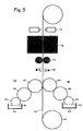
- Figure 5 shows an advantageous arrangement for producing the structures 6, 7 in accurate register relationship, if that is effected by structuring of the layers 8 and 9 ( Figure 1 ).
- the arrangement includes two printing mechanisms 59, 60 which are known from the letterset process and which each have an ink bath 61 and 62 respectively, an Anilox roller 63 and 64 respectively, a print cylinder 65 and 66 respectively and a rubber cylinder 67 and 68 respectively and which are so arranged that the carrier foil 3 in the form of foil strip is guided between the two rubber cylinders 67 and 68.
- the print cylinders 65 and 66 which contain the print patterns are uniformly provided by way of the Anilox rollers 63, 64 with a predetermined liquid agent 69 from the ink bath 61 and 62 respectively.
- the agent 69 is then transferred by the cylinder 65 and 66 respectively in accordance with the corresponding print pattern onto the respective rubber cylinder 67, 68 and from same onto the corresponding surface 4, 5 ( Figure 1 ) of the carrier foil 3.
- the drive system for the two printing mechanisms 59, 60 is coupled so that the print cylinders 65, 66 and the rubber cylinders 67, 68 rotate synchronously.
- the liquid agent 69 can be the above-described protective lacquer or the above-described lacquer layer.
- the liquid agent 69 may however also be a lye which directly dissolves the layer 8 or 9, which is possible in particular if the layers 8, 9 are thin metallic layers of for example aluminium.
- the arrangement also has nozzles 70 which spray for example water onto the layers 8 and 9 which are already structured by means of the lye, in order to remove residues of the lye.
- the carrier foil 3 which is now provided with the structures 6 and 7 is dried by means of a drying device which includes for example squeeze rollers 71 and an oven 72.
- the arrangement advantageously also has sensors 73 for checking the register accuracy of the structures 6 and 7 so that the printing mechanisms 59, 60 can be accurately adjusted.
Abstract
Description
- The invention concerns an optical information carrier.
- Such optical information carriers with an optical diffraction structure are suitable for example for increasing the level of safeguard against forgery and for conspicuously identifying articles of all kinds and can be used in particular in relation to security and bond documents, passes, payment means and similar articles to be safeguarded.
- European patent specification
EP 328 086 - European patent specification
EP 012 375 - British
patent specification GB 2 237 774 - German laid-open application (DE-OS) No.
23 50 109 discloses a foil serving as a holographic recording medium. Formed both in the underside and in the top side of the foil are relief patterns which represent items of holographic information. The holograms are recorded using a special procedure so that the holograms which are stored on both sides of the foil can be read off separately. Optical correlation between the holograms on one side and the holograms on the other side is prevented as far as possible by virtue of the special recording procedure. - Embodiments of the invention are described in greater detail hereinafter with reference to the drawing
figures 1 to 5 . A short description of the drawings: - Figure 1
- shows an information carrier with optically effective structures for producing moiré effects (which is not an embodiment according to the claims),
- Figure 2
- shows an information carrier with an integrated microlens,
- Figure 3
- shows an information carrier acting as a retroreflector,
-
WO94/27254 fig. 5 ) an optical information carrier in the form of a composite laminate with a carrier which is approximately transparent for light in a predetermined spectral range. An array of micro-images is provided at the underside of the carrier. Further the underside of the carrier bears a base layer, the refractive index of which differs from the refractive index of the carrier in at least a portion of the electromagnetic spectrum. The micro-images are surface portions of the array and arranged in mutually juxtaposed relationship and can vary from one surface portion to the next associated surface portion. The topside of the carrier is provided with optically effective, microscopic relief structures which form at least one micro-lens, the thickness of the carrier approximately corresponding to the focal length of the micro-lens and being at least 20 micrometers. A predetermined number of surface portions is associated with each micro-lens to form one of a plurality of juxtaposed information units, each of the surface portions associated with one of the micro-lenses forming a pixel of an image composed of the micro-images so that at a fixed direction of incidence of an incident light beam the pixels form one image, the image conveying different optical impressions at different viewing angles. The micro-images are printed to the underside of the carrier, whereas the micro-lenses on the topside of the carrier can be formed in a respective molding step. The fact that the micro-images have to be printed necessarily means a certain restriction as to the optical effects which can be achieved. As there is no base layer in the area of the micro-images, there can only be reached a limited degree of contrast. - It is an object of the present invention to propose an optical information carrier which has optical security features that cannot be copied using holographic methods and which can be easily produced in large numbers, but which additionally gives the possibility of providing easily and clearly recognizable security features.
- This object is achieved with an optical information carrier comprising the features of
claim 1, advantageous configurations being subject of the depending claims. - The basic idea underlying the invention is the idea of providing the optical information carrier with two optically effective structures, which are arranged in different plains and which jointly produce a characteristic optical effect. One of the two structures is a microscopically fine relief structure on one side of the carrier foil, whereas the other structure forms micro-lenses. As proper realization of the inventive concept necessitates a high level of register accuracy between the two structures (on both sides of the carrier foil), forgery of a respective information carrier is particularly difficult.
- Figure 4
- shows an arrangement for embossing relief structures in register relationship, and
- Figure 5
- shows an arrangement for applying structured layers in register relationship.
- In the drawings, which are not to scale,
Figure 1 shows a view in cross-section of anoptical information carrier 1 in the form of acomposite laminate 2. The core of thecomposite laminate 2 is formed by acarrier foil 3 whose thickness d is at least 20 micrometres. Thecarrier foil 3 may however also be substantially thicker, for example 100 or 200 micrometres. The underside 4 and thetop side 5 of thecarrier foil 3 are provided with opticallyeffective structures effective structures top side 4 and 5 respectively and/or by applyingfurther layers 8, 9 to the underside and thetop side 4 and 5 respectively. - The
basal structures 6 on the underside 4 of thecarrier foil 3 are microscopicallyfine relief structures 10 which are covered by thebase layer 8. The optical refractive index of thebase layer 8 differs from the refractive index of thecarrier foil 3 at least in a portion of the visible electromagnetic spectrum. The geometrical parameters of therelief structures 10, line spacing and profile height, are typically in the range of some tenths of a micrometre to some micrometres. The profile height however may also be only some tens of nanometres. Therelief structures 10 diffract impinging light and produce optical-diffraction effects which can be perceived by the human eye. The iuminosity of therelief structures 10 depends on the difference in the refractive indices of thelayers relief structures 10. In the unclaimed example ofFig. 1 , thetop structures 7 on thetop side 5 of thecarrier foil 3 are formed by the cover layer 9 only partially covering thecarrier foil 3. Accordingly thetop structures 7 form on the top side 5 a microscopic pattern comprising surfaces which are formed by the cover layer 9 and which cover thetop side 5, and gaps where thetop side 5 is exposed. The dimensions of the gaps, in an x-direction, are in the range of ten micrometres and more, typically in the range of 20 to 30 micrometres. In another direction the dimensions of the gaps can be substantially greater, for example a millimetre. The cover layer 9 is not transparent in relation to visible light. It is for example a thin metal layer or a dyestuff layer applied by a printing procedure. - In general the
layer 8 is covered by anadhesive layer 12 so that theinformation carrier 1 can be directly joined to the surface of abase card 13, for example a banknote, an identity card, a document or the like. Thelayers composite laminate 2 which cannot be separated without being destroyed so that items of information which are present in the form of thestructures composite laminate 2 in such a way as to be safeguarded against forgery. - When illuminated under normal illumination conditions, for example in daylight, the
composite laminate 2 ofFig.1 produces so-called moiré effects. - The
relief structures 10 are for example a grating with straight or curved grooves. The use ofrelief structures 10 with an asymmetrical, for example sawtooth-shaped profile configuration provides that the intensity of the light which is diffracted into the positive diffraction orders is greater than the intensity of the light which is diffracted into the negative diffraction orders so that the luminosity of the play of colours when the information carrier is turned through an angle of 180° alters markedly. If the grating parameters of therelief structures 10 on the underside 4 locally depend on the location, the colour pattern produced with a given angle of incidence of thelight 11 exhibits locally different colours. - If the
base layer 8 and theadhesive layer 12 are in the form of transparent lacquer layers and if the free surface area which is not covered by the cover layer 9 is of a sufficiently large proportion, then the surface of thebase card 13 and therewith for example information printed on thebase card 13 are visible through thecomposite laminate 2 which is glued in position. If thebase layer 8 in contrast is a metallic layer which almost completely reflects impinging light, then the glued-oncomposite laminate 2 conceals the surface of thebase card 13. - The optical information carrier described with reference to
Figure 1 is distinguished by a high level of safeguard against forgery as thestructures 6 arranged in the lower plane are not accessible either optically or in any other fashion. Thestructures 6 are however as equally significant as thestructures 7 for producing the desired light guide and filter effects. -
Figure 2 is a perspective view showing thesurfaces 4 and 5 of thecarrier foil 3. Amicrolens 19, in the present case a Fresnel lens, in the configuration of a macroscopic relief structure, is formed into thesurface 5 as the structure 7 (Figure 1 ). Nine surface portions 20 are arranged matrix-like in mutually juxtaposed relationship on the underside 4 as the structure 6 (Figure 1 ), wherein the central one of the nine surface portions 20 is disposed approximately at the focal point of themicrolens 19. The information present in the surface portions 20 is symbolically represented in the drawing by letters. The focal length of themicrolens 19 and the thickness d of thecarrier foil 3 are therefore matched to each other. With a typical diameter of themicrolens 19 of 100 µm and a profile height of about 5 µm, focal lengths in the range of 100 µm to 250 µm can readily be achieved. Formed in the surface portions 20 aremicroscopic relief structures 10 which can fulfill various functions. Themicrolens 19 and the associated nine surface portions 20 form an information unit. Theinformation carrier 1 preferably contains a plurality of mutually juxtaposedmicrolenses 19 with associated surface portions 20. - The
microlens 19 focusses incident light 11 in dependence on the direction of incidence onto one surface portion 20 or another so that only therelief structures 10 of a single surface portion. 20 are illuminated. In aninformation carrier 1 which is advantageously in the form of an optical ROM, thediffraction structures 10 diffract light into one or more beam portions 21 of predetermined direction. Therelief structures 10 vary from one surface portion 20 to another, according to the stored information. The information stored in the surface portion 20 can be ascertained by machine, by means of a reading device which is designed to analyse the levels of intensity of the beam portions 21. If for example the predetermined number of directions into which light can be diffracted as a beam portion 21 is eight, then each surface portion 20 can store eight bits: in the case of a bit with the binary value "1", light is diffracted in the corresponding direction, while in the case of a bit with the binary value "0", no light is diffracted into the corresponding direction. - The information carrier can also be in the form of a WORM storage means. In that case only a single bit can be stored in each surface portion 20. Immediately after production of the
information carrier 1 each surface portion 20 has an identicalintact relief structure 10 which diffracts light in at least one predetermined direction as a beam portion 21. Theintact relief structure 10 represents a bit "1". The operation of reading the bit is effected with a low-intensity light beam. With a high-intensity light beam which is produced by the reading device which is switched into a high-power mode, therelief structure 10 can be altered insofar as it cannot diffract light, or it can no longer diffract sufficient light, in the predetermined directions, as beam portions 21: the alteredrelief structure 10 represents a bit "0". Comparatively little energy is required to write a bit "0" as themicrolens 19 focusses the light onto therelief structure 10 to be destroyed. In our example, nine surface portions 20 serving as a storage cell for a single bit can be read with eachmicrolens 19, wherein addressing of the correct surface portion 20 is effected by adjusting the direction of incidence of the light 11. - In another configuration the surface portions 20, arranged at the same location, of all information units, respectively form pixels of an image. Therefore nine images can be represented with nine surface portions 20, wherein one or other of the nine images is respectively made visible in dependence on the direction of
incident light 11. An image is composed of diffraction structures, wherein the parameters of the diffraction structures may vary from one pixel to another, that is to say from the associated surface portion 20 to the next associated surface portion 20. Such an image can therefore produce kinematic diffraction effects, that is to say, with a fixed direction of incidence of the light, at different viewing angles, the image conveys different optical impressions, as are known for example from European patent specificationsEP 105 099 EP 375 833 -
Figure 3 shows theinformation carrier 1 in which thetop side 5 of thecarrier foil 3 has once again as the structure 7 arelief structure 15 which acts as amicrolens 19. The underside 4 has as thestructure 6 therelief structure 10 which is metallised with thelayer 8 and which acts as areflector 22.Light 11 which is incident in parallel relationship is focussed by themicrolens 19 onto a given point P on thereflector 22 in dependence on the direction of incidence, as a plurality ofbeam portions relief structure 10 of thereflector 22 is now such that thebeam portion 23 which locally impinges on the point P is reflected and/or diffracted in the opposite direction to thebeam portion 24 impinging on the point P. That provides that the light impinging onto themicrolens 19 is reflected in the opposite direction. The combination of themicrolens 19 and thereflector 22 thus forms a retroreflector. The retroreflector can be produced in a simple fashion, for example by embossing therelief structures carrier foil 3 of thermoplastic material. - An example of use is a banknote in which a plurality of retroreflectors are arranged along a track at predetermined spacings, for example like a bar code. The information stored in the bar code can be read out with an optical reading device when the track is moved past the reading head. As the light reflected at the retroreflectors is always reflected back into the direction of incidence, the information can be read without any difficulty, even in the event of the banknote fluttering as a result of a high speed of transportation movement.
-
Figure 4 shows an arrangement for embossing relief structures in accurate register relationship. The arrangement includes atransport device 56 for thecarrier foil 3 which is in the form of a foil strip, and twoembossing cylinders embossing cylinders embossing cylinders embossing cylinders embossing cylinders relief structures top side 5 respectively of thecarrier foil 3. Theembossing cylinders carrier foil 3 is advantageously in the form of a composite laminate which has a temperature-resistant carrier layer, for example of polyester, arranged between two embossable lacquer layers. - For the production of cheques with a fixed monetary value, two basic processes are known, for providing the embossed
top side 5 with the structured cover layer 9 (Figure 12), more specifically selective removal of the cover layer 9 which is applied over the entire surface area or local application of the cover layer 9. Selective removal of the cover layer 9 can be effected by using a printing procedure to apply a structured protective lacquer to the cover layer 9. The surfaces of the cover layer 9, which are not printed upon, are then removed in a solvent bath, for example by etching. Finally the protective lacquer is removed again. Local application of the cover layer 9 can be effected by those surfaces which are not to be covered by the cover layer 9 being printed upon with a lacquer layer. Thereupon thecarrier foil 3 which has been treated in that way is coated over its entire surface area with the cover layer 9, for example by vapour deposition. The lacquer layer together with the cover layer 9 disposed thereon are removed by means of a washing process in a selectively attacking solvent. -
Figure 5 shows an advantageous arrangement for producing thestructures layers 8 and 9 (Figure 1 ). The arrangement includes twoprinting mechanisms ink bath Anilox roller print cylinder rubber cylinder carrier foil 3 in the form of foil strip is guided between the tworubber cylinders print cylinders Anilox rollers liquid agent 69 from theink bath agent 69 is then transferred by thecylinder respective rubber cylinder Figure 1 ) of thecarrier foil 3. The drive system for the twoprinting mechanisms print cylinders rubber cylinders - The
liquid agent 69 can be the above-described protective lacquer or the above-described lacquer layer. Theliquid agent 69 may however also be a lye which directly dissolves thelayer 8 or 9, which is possible in particular if thelayers 8, 9 are thin metallic layers of for example aluminium. In that case the arrangement also hasnozzles 70 which spray for example water onto thelayers 8 and 9 which are already structured by means of the lye, in order to remove residues of the lye. Thecarrier foil 3 which is now provided with thestructures example squeeze rollers 71 and anoven 72. The arrangement advantageously also hassensors 73 for checking the register accuracy of thestructures printing mechanisms
Claims (10)
- An optical information carrier (1) which is in the form of a composite laminate (2) with a carrier foil (3) which is approximately transparent for light in a predetermined spectral range, wherein microscopically fine relief structures (10), which are subdivided into surface portions (20) which are arranged in mutually juxtaposed relationship and have parameters, which can vary from the one surface portion (20) to the next associated surface portion (20), are formed into the underside (4) of the carrier foil (3), the underside (4) of the carrier foil (3) being coated with a base layer (8) covering the relief structures (10) on the underside (4) of the carrier foil (3), the refractive index of the base layer (8) differing from the refractive index of the carrier foil (3) in at least a portion of the electromagnetic spectrum, the relief structures (10) on the underside (4) at least partially reflecting and diffracting light (11) which has penetrated into the composite laminate (2), wherein the top side (5) of the carrier foil (3) is provided with optically effective, macroscopic relief structures (7) which form at least one micro-lens (19), the thickness (d) of the carrier foil (3) approximately corresponding to the focal length of the micro-lens (19) and being at least 20 micrometers, wherein a predetermined number of surface portions (20) is associated with each micro-lens (19) and form one of a plurality of juxtaposed information units, wherein each of the surface portions (20) associated with one of the micro-lenses (19) forms a pixel of an image composed of the relief structures (10), and wherein at a fixed direction of incidence of an incident light beam (11) the pixels form one image, the image conveying different optical impressions at different viewing angles.
- The optical information carrier according to claim 1 characterized in that the diffraction properties of the relief structures (10) are individually irreversibly alterable by applying thermal energy according to a stored information and form an optical WORM storage means, in that the surface portions (20) are individually illuminated by varying the direction of incidence of an incident light beam (11) in order to ascertain the information.
- The optical information carrier according to claims 1 or 2, characterized in that the relief structures (10) vary from one surface portion (20) to another according to a stored information and form an optical ROM, and in that the surface portions (20) are individually illuminated by varying the direction of incidence of an incident light beam (11) in order to ascertain the information.
- The optical information carrier according to any of the preceding claims, characterized in that the relief structures (10) on the underside (4) form at least one reflector (22) and that each micro-lens (19) has associated therewith a reflector (22) which together form a retro-reflector which reflects light (11) incident in parallel relationship from a direction of incidence back into the direction of incidence.
- The optical information carrier according to claim 4, characterized in that a plurality of the retro-reflectors composed of the micro-lens (19) and its associated reflector (22), are arranged along a track at predetermined spacings like a bar code.
- The optical information carrier according to any of the preceding claims characterized in that the optically effective structures (7) on the top side and the relief structures (10) on the underside (4) are embossed into the carrier foil (3) in accurate register relationship.
- The optical information carrier according to any of the preceding claims characterized in that the base layer (8) is a metallic layer which almost completely reflects impinging light (11).
- The optical information carrier according to any of the preceding claims characterized in that the micro-lenses (19) is a Fresnel lens.
- The optical information carrier according to any of the preceding claims characterized in that the micro-lenses (19) have a focal length in the range of 100 micrometers to 250 micrometers.
- The optical information carrier according to any of the preceding claims characterized in that the base layer (8) of the composite laminate (2) is covered by an adhesive layer (12) in order to affix the composite laminate (2) to a base card (13) or document (13) or substrate (13)
Applications Claiming Priority (5)
| Application Number | Priority Date | Filing Date | Title |
|---|---|---|---|
| CH336995 | 1995-11-28 | ||
| CH03369/95A CH691750A5 (en) | 1995-11-28 | 1995-11-28 | Optical information carrier made of composite laminate with carrier foil |
| CH03567/95A CH690529A5 (en) | 1995-12-18 | 1995-12-18 | Optical information carrier made of composite laminate with carrier foil |
| CH356795 | 1995-12-18 | ||
| EP96939036A EP0871574B1 (en) | 1995-11-28 | 1996-11-14 | Optical information carrier |
Related Parent Applications (2)
| Application Number | Title | Priority Date | Filing Date |
|---|---|---|---|
| EP96939036A Division EP0871574B1 (en) | 1995-11-28 | 1996-11-14 | Optical information carrier |
| EP96939036.8 Division | 1997-06-05 |
Publications (3)
| Publication Number | Publication Date |
|---|---|
| EP1182054A2 EP1182054A2 (en) | 2002-02-27 |
| EP1182054A3 EP1182054A3 (en) | 2004-08-11 |
| EP1182054B1 true EP1182054B1 (en) | 2009-05-13 |
Family
ID=25692849
Family Applications (3)
| Application Number | Title | Priority Date | Filing Date |
|---|---|---|---|
| EP01122061A Expired - Lifetime EP1182055B1 (en) | 1995-11-28 | 1996-11-14 | Optical information carrier |
| EP96939036A Expired - Lifetime EP0871574B1 (en) | 1995-11-28 | 1996-11-14 | Optical information carrier |
| EP01121968A Expired - Lifetime EP1182054B1 (en) | 1995-11-28 | 1996-11-14 | Optical information carrier |
Family Applications Before (2)
| Application Number | Title | Priority Date | Filing Date |
|---|---|---|---|
| EP01122061A Expired - Lifetime EP1182055B1 (en) | 1995-11-28 | 1996-11-14 | Optical information carrier |
| EP96939036A Expired - Lifetime EP0871574B1 (en) | 1995-11-28 | 1996-11-14 | Optical information carrier |
Country Status (7)
| Country | Link |
|---|---|
| EP (3) | EP1182055B1 (en) |
| AT (3) | ATE357345T1 (en) |
| AU (1) | AU7624496A (en) |
| CA (1) | CA2238384C (en) |
| DE (3) | DE69636991T2 (en) |
| ES (1) | ES2171747T3 (en) |
| WO (1) | WO1997019820A1 (en) |
Cited By (14)
| Publication number | Priority date | Publication date | Assignee | Title |
|---|---|---|---|---|
| US7791802B2 (en) | 2004-02-19 | 2010-09-07 | Illumina, Inc. | Optical identification element having a non-waveguide substrate |
| US7796333B2 (en) | 2004-11-17 | 2010-09-14 | Illumina, Inc. | Encoded microparticles and a method for fabricating |
| US7843567B2 (en) | 2003-01-22 | 2010-11-30 | Illumina, Inc. | Methods of identifying an analyte and nucleic acid analysis |
| US7898735B2 (en) | 2002-09-12 | 2011-03-01 | Illumina, Inc. | Methods and systems for writing an optical code within or on a fiber substrate |
| US7900836B2 (en) | 2002-08-20 | 2011-03-08 | Illumina, Inc. | Optical reader system for substrates having an optically readable code |
| DE102011121588A1 (en) | 2011-12-20 | 2013-06-20 | Giesecke & Devrient Gmbh | Security element for security papers, documents of value or the like |
| US8470605B2 (en) | 2002-09-12 | 2013-06-25 | Illumina, Inc. | Optical reader for reading encoded microparticles |
| US8498052B2 (en) | 2002-08-20 | 2013-07-30 | Illumina, Inc. | Composition including an item and an encoded optical substrate and a method for identifying an item |
| US8565475B2 (en) | 2003-08-20 | 2013-10-22 | Illumina, Inc. | Optical system and method for reading encoded microbeads |
| WO2014012667A1 (en) | 2012-07-20 | 2014-01-23 | Giesecke & Devrient Gmbh | Security element for security papers, value documents or the like |
| EP2927715A1 (en) | 2014-04-04 | 2015-10-07 | Giesecke & Devrient GmbH | Safety element for security papers, valuable documents or the like |
| EP3184319A1 (en) | 2015-12-23 | 2017-06-28 | Giesecke & Devrient GmbH | Safety element for security papers, valuable documents or the like |
| WO2021057574A1 (en) * | 2019-09-29 | 2021-04-01 | 中钞特种防伪科技有限公司 | Multilayer body optical anti-counterfeiting element and fabrication method therefor |
| US11511559B2 (en) | 2014-12-12 | 2022-11-29 | Giesecke+Devrient Currency Technology Gmbh | Optically variable security element |
Families Citing this family (81)
| Publication number | Priority date | Publication date | Assignee | Title |
|---|---|---|---|---|
| US5683774A (en) | 1994-12-09 | 1997-11-04 | Minnesota Mining And Manufacturing Company | Durable, tamper resistant security laminate |
| US5656360A (en) * | 1996-02-16 | 1997-08-12 | Minnesota Mining And Manufacturing Company | Article with holographic and retroreflective features |
| US6024455A (en) * | 1998-01-13 | 2000-02-15 | 3M Innovative Properties Company | Reflective article with concealed retroreflective pattern |
| US6045230A (en) * | 1998-02-05 | 2000-04-04 | 3M Innovative Properties Company | Modulating retroreflective article |
| DE19926689A1 (en) * | 1999-06-11 | 2000-12-14 | Hsm Gmbh | Optical authenticity feature |
| US7047883B2 (en) | 2002-07-15 | 2006-05-23 | Jds Uniphase Corporation | Method and apparatus for orienting magnetic flakes |
| US11768321B2 (en) | 2000-01-21 | 2023-09-26 | Viavi Solutions Inc. | Optically variable security devices |
| PT1849621E (en) † | 2000-01-21 | 2014-06-03 | Jds Uniphase Corp | Optically variable security devices |
| GB0015873D0 (en) | 2000-06-28 | 2000-08-23 | Rue De Int Ltd | Optically variable security device |
| DE10036505A1 (en) * | 2000-07-27 | 2003-08-14 | Orga Kartensysteme Gmbh | Optically effective structure for personalizing cards and. Like., And methods for their production |
| DE10124630A1 (en) * | 2001-05-18 | 2002-11-21 | Giesecke & Devrient Gmbh | Security, especially banknote, with printed symbols and security element, is coated with mat protective varnish except over security element |
| CZ20041001A3 (en) † | 2002-04-03 | 2005-03-16 | De La Rue International Limited | Optically variable protective element and process for producing thereof |
| US11230127B2 (en) | 2002-07-15 | 2022-01-25 | Viavi Solutions Inc. | Method and apparatus for orienting magnetic flakes |
| UA81253C2 (en) * | 2002-07-24 | 2007-12-25 | Fabriano Securities Srl | Security element for documents, method of its production (variants) and document with this security element |
| US7923260B2 (en) | 2002-08-20 | 2011-04-12 | Illumina, Inc. | Method of reading encoded particles |
| US7872804B2 (en) | 2002-08-20 | 2011-01-18 | Illumina, Inc. | Encoded particle having a grating with variations in the refractive index |
| US7901630B2 (en) | 2002-08-20 | 2011-03-08 | Illumina, Inc. | Diffraction grating-based encoded microparticle assay stick |
| US9458324B2 (en) | 2002-09-13 | 2016-10-04 | Viava Solutions Inc. | Flakes with undulate borders and method of forming thereof |
| US9164575B2 (en) | 2002-09-13 | 2015-10-20 | Jds Uniphase Corporation | Provision of frames or borders around pigment flakes for covert security applications |
| US8025952B2 (en) | 2002-09-13 | 2011-09-27 | Jds Uniphase Corporation | Printed magnetic ink overt security image |
| DE10254500B4 (en) | 2002-11-22 | 2006-03-16 | Ovd Kinegram Ag | Optically variable element and its use |
| DE10254499B4 (en) * | 2002-11-22 | 2005-12-22 | Ovd Kinegram Ag | Layer arrangement with a lens-like effect generating diffractive optical effective structure |
| ITMI20030929A1 (en) * | 2003-05-08 | 2004-11-09 | Mantegazza A Arti Grafici | SAFETY ELEMENT OF THE WIRE TYPE, TAPE AND SIMILAR, FOR SECURITY DOCUMENTS IN GENERAL |
| US7090913B2 (en) | 2003-05-16 | 2006-08-15 | Eastman Kodak Company | Security device with specular reflective layer |
| FR2856339B1 (en) * | 2003-06-23 | 2006-05-26 | Banque De France | SECURITY BAND FOR DOCUMENTATION AND SECURE DOCUMENT |
| DE10334310A1 (en) * | 2003-07-28 | 2005-02-24 | Giesecke & Devrient Gmbh | Security paper for the production of value documents |
| DE202004021714U1 (en) * | 2003-11-21 | 2010-09-23 | Visual Physics, Llc | Micro-optical security and image presentation system |
| US8867134B2 (en) | 2003-11-21 | 2014-10-21 | Visual Physics, Llc | Optical system demonstrating improved resistance to optically degrading external effects |
| AT501989B1 (en) | 2004-03-26 | 2010-04-15 | Hueck Folien Gmbh | SAFETY FEATURES WITH CHARACTERISTICS VISIBLE UNDER A SPECIFIC OVERVIEW |
| WO2005092635A1 (en) | 2004-03-29 | 2005-10-06 | Glud & Marstrand A/S | A method of producing a composite surface and an article having a composite surface |
| DE102004045211B4 (en) | 2004-09-17 | 2015-07-09 | Ovd Kinegram Ag | Security document with electrically controlled display element |
| DE102004061635A1 (en) † | 2004-12-17 | 2006-07-06 | Giesecke & Devrient Gmbh | Card-shaped data carrier |
| DE102005028162A1 (en) † | 2005-02-18 | 2006-12-28 | Giesecke & Devrient Gmbh | Security element for protecting valuable objects, e.g. documents, includes focusing components for enlarging views of microscopic structures as one of two authenication features |
| EP1698483A1 (en) * | 2005-03-01 | 2006-09-06 | Hueck Folien GmbH & Co. KG | Interactive packaging material |
| TWI402106B (en) | 2005-04-06 | 2013-07-21 | Jds Uniphase Corp | Dynamic appearance-changing optical devices (dacod) printed in a shaped magnetic field including printable fresnel structures |
| DE102005017170B4 (en) * | 2005-04-13 | 2010-07-01 | Ovd Kinegram Ag | Transfer film, process for their preparation and multilayer body and its use |
| DE102005017169B4 (en) | 2005-04-13 | 2023-06-22 | Ovd Kinegram Ag | transfer film |
| EP1767381B1 (en) | 2005-09-20 | 2008-11-05 | Alcan Technology & Management Ltd. | Article with optical effect |
| DE102005052326A1 (en) * | 2005-11-02 | 2007-05-03 | Giesecke & Devrient Gmbh | Security element for security papers, value documents, has open image information and hidden image information selectable by illumination of security elements whereby rendering range with first image element and second image element |
| EP1826708A1 (en) * | 2006-02-24 | 2007-08-29 | Maurer Electronics Gmbh | Card shaped data carrier |
| US7830575B2 (en) | 2006-04-10 | 2010-11-09 | Illumina, Inc. | Optical scanner with improved scan time |
| US8488242B2 (en) | 2006-06-20 | 2013-07-16 | Opsec Security Group, Inc. | Optically variable device with diffraction-based micro-optics, method of creating the same, and article employing the same |
| DE102006061905A1 (en) * | 2006-12-28 | 2008-07-03 | Zintzmeyer, Jörg | Safety member for use in authenticity certificates or securities, has mask pattern and image pattern aligned with each other such that different regions of image pattern are viewable by mask pattern during viewing of surface of mask pattern |
| DE102007039996B4 (en) * | 2007-02-07 | 2020-09-24 | Leonhard Kurz Stiftung & Co. Kg | Security element for a security document and method for its production |
| DE102007037982A1 (en) * | 2007-08-10 | 2009-02-12 | Bundesdruckerei Gmbh | Security document with watermarked structure |
| KR100944338B1 (en) * | 2007-12-20 | 2010-03-02 | 한국조폐공사 | A security film including diffractive lens array and a security document using thereof |
| DE102008008685A1 (en) | 2008-02-12 | 2009-08-13 | Giesecke & Devrient Gmbh | Security element and method for its production |
| JP2009193069A (en) | 2008-02-13 | 2009-08-27 | Jds Uniphase Corp | Medium for laser printing including optical special effect flake |
| DE102008013167A1 (en) | 2008-03-07 | 2009-09-10 | Giesecke & Devrient Gmbh | Security element and method for its production |
| DE102009031387A1 (en) * | 2009-07-01 | 2011-01-05 | Giesecke & Devrient Gmbh | Security element and manufacturing method therefor |
| ES2458346T3 (en) | 2009-12-18 | 2014-05-05 | Orell Füssli Sicherheitsdruck Ag | Security document with optical waveguide |
| DE102010050031A1 (en) | 2010-11-02 | 2012-05-03 | Ovd Kinegram Ag | Security element and method for producing a security element |
| CA2825655C (en) | 2011-01-28 | 2019-04-30 | Crane & Co., Inc. | A laser marked device |
| EP2745165B9 (en) | 2011-08-19 | 2018-07-18 | Visual Physics, LLC | Optionally transferable optical system with a reduced thickness |
| US10195891B2 (en) | 2011-09-26 | 2019-02-05 | Crane Security Technologies, Inc. | Method for producing a composite web and security devices prepared from the composite web |
| DK2802450T3 (en) | 2012-01-12 | 2019-03-25 | Viavi Solutions Inc | Article with a dynamic frame consisting of decorated pigment flakes |
| US8834004B2 (en) | 2012-08-13 | 2014-09-16 | 3M Innovative Properties Company | Lighting devices with patterned printing of diffractive extraction features |
| JP6053932B2 (en) | 2012-08-17 | 2016-12-27 | ビジュアル フィジクス エルエルシー | The process of transferring the microstructure to the final substrate |
| RU2506168C1 (en) * | 2012-10-04 | 2014-02-10 | Сергей Николаевич Максимовский | Method of creation on sheet material of iridescent image, and sheet material for its implementation |
| EP2969585B1 (en) | 2013-03-15 | 2019-04-24 | Visual Physics, LLC | Optical security device |
| US9873281B2 (en) | 2013-06-13 | 2018-01-23 | Visual Physics, Llc | Single layer image projection film |
| FR3011508B1 (en) * | 2013-10-08 | 2021-05-28 | Banque De France | SECURITY DOCUMENT INCLUDING A FILM WITH INTERFERENTIAL EFFECTS, PROCESS FOR DETERMINING THE AUTHENTICITY OF SUCH A DOCUMENT AND DEVICE FOR IMPLEMENTING SUCH A PROCESS. |
| RU2537837C1 (en) * | 2013-12-10 | 2015-01-10 | Сергей Николаевич Максимовский | Method of amplifying luminescence of iridescent image formed within sheet material |
| AU2015235889B2 (en) | 2014-03-27 | 2018-10-11 | Visual Physics, Llc | An optical device that produces flicker-like optical effects |
| US10766292B2 (en) | 2014-03-27 | 2020-09-08 | Crane & Co., Inc. | Optical device that provides flicker-like optical effects |
| DE112015002233B4 (en) * | 2014-05-13 | 2019-12-24 | Toppan Printing Co., Ltd. | Diffraction pattern transfer sheet and anti-counterfeiting medium using the same |
| EP3169531B1 (en) | 2014-07-17 | 2019-03-06 | Visual Physics, LLC | An improved polymeric sheet material for use in making polymeric security documents such as banknotes |
| KR102497982B1 (en) | 2014-09-16 | 2023-02-09 | 크레인 시큐리티 테크놀로지스, 인크. | Secure lens layer |
| KR20170110699A (en) | 2015-02-11 | 2017-10-11 | 크레인 앤 코, 인크 | Method for surface application of a security device to a substrate |
| CN110582412B (en) | 2017-02-10 | 2022-08-30 | 克瑞尼股份有限公司 | Machine readable optical security device |
| DE102017003281A1 (en) | 2017-04-04 | 2018-10-04 | Giesecke+Devrient Currency Technology Gmbh | Security element with relief structure and manufacturing method therefor |
| DE102017003603A1 (en) * | 2017-04-12 | 2018-10-18 | Giesecke+Devrient Currency Technology Gmbh | Security element with colored feature area |
| WO2018216700A1 (en) | 2017-05-22 | 2018-11-29 | 凸版印刷株式会社 | Information recording body and individual certifying body |
| RU2658492C1 (en) * | 2017-06-07 | 2018-06-21 | Сергей Николаевич Максимовский | Method of creating individual iridescent image for protection against forgery of identification document |
| DE102018207452A1 (en) | 2018-05-15 | 2019-11-21 | Audi Ag | Reflector for a vehicle for displaying at least one symbol, vehicle and manufacturing method |
| DE102018005447A1 (en) * | 2018-07-09 | 2020-01-09 | Giesecke+Devrient Currency Technology Gmbh | Optically variable security element with reflective surface area |
| DE102018005474A1 (en) * | 2018-07-09 | 2020-01-09 | Giesecke+Devrient Currency Technology Gmbh | Optically variable security element with reflective surface area |
| DE102018005454A1 (en) * | 2018-07-09 | 2020-01-09 | Giesecke+Devrient Currency Technology Gmbh | Optically variable security element with reflective surface area |
| DE102020000031A1 (en) * | 2020-01-03 | 2021-07-08 | Giesecke+Devrient Currency Technology Gmbh | Optically variable security element |
| DE102020004091A1 (en) | 2020-07-07 | 2022-01-13 | Giesecke+Devrient Currency Technology Gmbh | Optically variable security element |
| DE102020005932A1 (en) * | 2020-09-28 | 2022-03-31 | Giesecke+Devrient Currency Technology Gmbh | Optically variable security element with reflective surface area |
Family Cites Families (11)
| Publication number | Priority date | Publication date | Assignee | Title |
|---|---|---|---|---|
| US3552853A (en) * | 1968-07-01 | 1971-01-05 | Chain Lakes Res Assoc | Hologramic identification system |
| US3790245A (en) * | 1972-10-12 | 1974-02-05 | Rca Corp | Double-sided holographic replicas |
| DE2853953A1 (en) * | 1978-12-14 | 1980-07-03 | Hoechst Ag | IDENTIFICATION CARD |
| DE3166630D1 (en) * | 1981-02-03 | 1984-11-15 | Landis & Gyr Ag | Method for preventing the sucessful forgery of documents and device therefor |
| DE3422908C2 (en) * | 1984-06-20 | 1986-04-30 | Leonhard Kurz GmbH & Co, 8510 Fürth | Embossing foil, in particular hot stamping foil, with a surface that can be written on |
| US5145212A (en) * | 1988-02-12 | 1992-09-08 | American Banknote Holographics, Inc. | Non-continuous holograms, methods of making them and articles incorporating them |
| ES2217047T3 (en) * | 1989-01-31 | 2004-11-01 | Dai Nippon Insatsu Kabushiki Kaisha | CARD. |
| US5200253A (en) * | 1989-08-09 | 1993-04-06 | Dai Nippon Insatsu Kabushiki Kaisha | Hologram forming sheet and process for producing the same |
| DE3932505C2 (en) * | 1989-09-28 | 2001-03-15 | Gao Ges Automation Org | Data carrier with an optically variable element |
| GB8924111D0 (en) * | 1989-10-26 | 1989-12-13 | Amblehurst Ltd | Optical device |
| GB9309673D0 (en) * | 1993-05-11 | 1993-06-23 | De La Rue Holographics Ltd | Security device |
-
1996
- 1996-11-14 DE DE69636991T patent/DE69636991T2/en not_active Expired - Lifetime
- 1996-11-14 AT AT01122061T patent/ATE357345T1/en not_active IP Right Cessation
- 1996-11-14 ES ES96939036T patent/ES2171747T3/en not_active Expired - Lifetime
- 1996-11-14 EP EP01122061A patent/EP1182055B1/en not_active Expired - Lifetime
- 1996-11-14 AU AU76244/96A patent/AU7624496A/en not_active Abandoned
- 1996-11-14 EP EP96939036A patent/EP0871574B1/en not_active Expired - Lifetime
- 1996-11-14 EP EP01121968A patent/EP1182054B1/en not_active Expired - Lifetime
- 1996-11-14 AT AT01121968T patent/ATE431260T1/en not_active IP Right Cessation
- 1996-11-14 WO PCT/EP1996/004987 patent/WO1997019820A1/en active IP Right Grant
- 1996-11-14 DE DE69620636T patent/DE69620636T2/en not_active Expired - Lifetime
- 1996-11-14 DE DE69637932T patent/DE69637932D1/en not_active Expired - Lifetime
- 1996-11-14 CA CA002238384A patent/CA2238384C/en not_active Expired - Fee Related
- 1996-11-14 AT AT96939036T patent/ATE215887T1/en active
Cited By (23)
| Publication number | Priority date | Publication date | Assignee | Title |
|---|---|---|---|---|
| US8333325B2 (en) | 2002-08-20 | 2012-12-18 | Illumina, Inc. | Optical reader system for substrates having an optically readable code |
| US8614852B2 (en) | 2002-08-20 | 2013-12-24 | Illumina, Inc. | Elongated microparticles having an optically detectable code configured to at least one of reflect or filter light |
| US8498052B2 (en) | 2002-08-20 | 2013-07-30 | Illumina, Inc. | Composition including an item and an encoded optical substrate and a method for identifying an item |
| US7900836B2 (en) | 2002-08-20 | 2011-03-08 | Illumina, Inc. | Optical reader system for substrates having an optically readable code |
| US7898735B2 (en) | 2002-09-12 | 2011-03-01 | Illumina, Inc. | Methods and systems for writing an optical code within or on a fiber substrate |
| US8470605B2 (en) | 2002-09-12 | 2013-06-25 | Illumina, Inc. | Optical reader for reading encoded microparticles |
| US8049893B2 (en) | 2003-01-22 | 2011-11-01 | Illumina, Inc. | Methods of identifying analytes and using encoded particles |
| US9268983B2 (en) | 2003-01-22 | 2016-02-23 | Illumina, Inc. | Optical system and method for reading encoded microbeads |
| US7843567B2 (en) | 2003-01-22 | 2010-11-30 | Illumina, Inc. | Methods of identifying an analyte and nucleic acid analysis |
| US8565475B2 (en) | 2003-08-20 | 2013-10-22 | Illumina, Inc. | Optical system and method for reading encoded microbeads |
| US7791802B2 (en) | 2004-02-19 | 2010-09-07 | Illumina, Inc. | Optical identification element having a non-waveguide substrate |
| US7796333B2 (en) | 2004-11-17 | 2010-09-14 | Illumina, Inc. | Encoded microparticles and a method for fabricating |
| WO2013091858A1 (en) | 2011-12-20 | 2013-06-27 | Giesecke & Devrient Gmbh | Security element for security papers, documents of value, or similar |
| DE102011121588A1 (en) | 2011-12-20 | 2013-06-20 | Giesecke & Devrient Gmbh | Security element for security papers, documents of value or the like |
| US9718297B2 (en) | 2011-12-20 | 2017-08-01 | Giesecke & Devrient Gmbh | Security element for security papers, value documents or the like |
| WO2014012667A1 (en) | 2012-07-20 | 2014-01-23 | Giesecke & Devrient Gmbh | Security element for security papers, value documents or the like |
| DE102012014414A1 (en) | 2012-07-20 | 2014-01-23 | Giesecke & Devrient Gmbh | Security element for security papers, documents of value or the like |
| EP2927715A1 (en) | 2014-04-04 | 2015-10-07 | Giesecke & Devrient GmbH | Safety element for security papers, valuable documents or the like |
| DE102014004941A1 (en) | 2014-04-04 | 2015-10-08 | Giesecke & Devrient Gmbh | Security element for security papers, documents of value or the like |
| US11511559B2 (en) | 2014-12-12 | 2022-11-29 | Giesecke+Devrient Currency Technology Gmbh | Optically variable security element |
| EP3184319A1 (en) | 2015-12-23 | 2017-06-28 | Giesecke & Devrient GmbH | Safety element for security papers, valuable documents or the like |
| DE102015016751A1 (en) | 2015-12-23 | 2017-06-29 | Giesecke & Devrient Gmbh | Security element for security papers, documents of value or the like |
| WO2021057574A1 (en) * | 2019-09-29 | 2021-04-01 | 中钞特种防伪科技有限公司 | Multilayer body optical anti-counterfeiting element and fabrication method therefor |
Also Published As
| Publication number | Publication date |
|---|---|
| EP1182055A3 (en) | 2004-08-11 |
| EP1182054A2 (en) | 2002-02-27 |
| WO1997019820A1 (en) | 1997-06-05 |
| DE69636991D1 (en) | 2007-05-03 |
| DE69637932D1 (en) | 2009-06-25 |
| EP0871574B1 (en) | 2002-04-10 |
| ATE431260T1 (en) | 2009-05-15 |
| ES2171747T3 (en) | 2002-09-16 |
| CA2238384C (en) | 2007-01-16 |
| EP1182055B1 (en) | 2007-03-21 |
| DE69636991T2 (en) | 2007-12-06 |
| ATE215887T1 (en) | 2002-04-15 |
| CA2238384A1 (en) | 1997-06-05 |
| AU7624496A (en) | 1997-06-19 |
| DE69620636T2 (en) | 2002-11-21 |
| EP0871574A1 (en) | 1998-10-21 |
| ATE357345T1 (en) | 2007-04-15 |
| DE69620636D1 (en) | 2002-05-16 |
| EP1182055A2 (en) | 2002-02-27 |
| EP1182054A3 (en) | 2004-08-11 |
Similar Documents
| Publication | Publication Date | Title |
|---|---|---|
| EP1182054B1 (en) | Optical information carrier | |
| US6060143A (en) | Optical information carrier | |
| US5882463A (en) | Method of applying a security element to a substrate | |
| US5310222A (en) | Optical device | |
| US5760961A (en) | Optical information carrier having diffractive features and diffraction modulation layers | |
| RU2230671C2 (en) | Foxing film | |
| US5142383A (en) | Holograms with discontinuous metallization including alpha-numeric shapes | |
| US5044707A (en) | Holograms with discontinuous metallization including alpha-numeric shapes | |
| EP0328086B2 (en) | Articles incorporating non-continuous holographs and methods of making them | |
| JP5727522B2 (en) | Security equipment | |
| US7894112B2 (en) | Security element with a diffraction structure having subareas representing recognizable information | |
| US5128779A (en) | Non-continuous holograms, methods of making them and articles incorporating them | |
| US7820269B2 (en) | Transfer film | |
| US5106125A (en) | Arrangement to improve forgery protection of credit documents | |
| US5714213A (en) | Securtiy element | |
| US5759420A (en) | Production of partially metallised grating structures | |
| EP0194042A2 (en) | Embossed articles | |
| US5538753A (en) | Security element | |
| CA2483794C (en) | Strip-shaped security element | |
| CN104249584A (en) | Optical anti-counterfeiting element | |
| KR100362350B1 (en) | Optical carrier with optical label | |
| JPH07320014A (en) | Information recording medium and its manufacture | |
| MXPA01009392A (en) | Decorative foil |
Legal Events
| Date | Code | Title | Description |
|---|---|---|---|
| PUAI | Public reference made under article 153(3) epc to a published international application that has entered the european phase |
Free format text: ORIGINAL CODE: 0009012 |
|
| AC | Divisional application: reference to earlier application |
Ref document number: 871574 Country of ref document: EP |
|
| AK | Designated contracting states |
Kind code of ref document: A2 Designated state(s): AT CH DE DK ES FI FR GB GR IE IT LI NL PT SE |
|
| AX | Request for extension of the european patent |
Free format text: LT;LV |
|
| PUAL | Search report despatched |
Free format text: ORIGINAL CODE: 0009013 |
|
| AK | Designated contracting states |
Kind code of ref document: A3 Designated state(s): AT CH DE DK ES FI FR GB GR IE IT LI NL PT SE |
|
| AX | Request for extension of the european patent |
Extension state: LT LV |
|
| 17P | Request for examination filed |
Effective date: 20050202 |
|
| AKX | Designation fees paid |
Designated state(s): AT CH DE ES FI FR GB IT LI NL SE |
|
| 17Q | First examination report despatched |
Effective date: 20050613 |
|
| RBV | Designated contracting states (corrected) |
Designated state(s): AT CH DE ES FI FR GB IT LI NL SE |
|
| 17Q | First examination report despatched |
Effective date: 20050613 |
|
| GRAP | Despatch of communication of intention to grant a patent |
Free format text: ORIGINAL CODE: EPIDOSNIGR1 |
|
| GRAS | Grant fee paid |
Free format text: ORIGINAL CODE: EPIDOSNIGR3 |
|
| RIN1 | Information on inventor provided before grant (corrected) |
Inventor name: STAUB, RENE Inventor name: TOMPKIN, WAYNE ROBERT |
|
| RAP1 | Party data changed (applicant data changed or rights of an application transferred) |
Owner name: OVD KINEGRAM AG |
|
| GRAA | (expected) grant |
Free format text: ORIGINAL CODE: 0009210 |
|
| AC | Divisional application: reference to earlier application |
Ref document number: 0871574 Country of ref document: EP Kind code of ref document: P |
|
| AK | Designated contracting states |
Kind code of ref document: B1 Designated state(s): AT CH DE ES FI FR GB IT LI NL SE |
|
| REG | Reference to a national code |
Ref country code: GB Ref legal event code: FG4D |
|
| REG | Reference to a national code |
Ref country code: CH Ref legal event code: EP Ref country code: CH Ref legal event code: NV Representative=s name: FIAMMENGHI-FIAMMENGHI |
|
| REF | Corresponds to: |
Ref document number: 69637932 Country of ref document: DE Date of ref document: 20090625 Kind code of ref document: P |
|
| REG | Reference to a national code |
Ref country code: SE Ref legal event code: TRGR |
|
| PG25 | Lapsed in a contracting state [announced via postgrant information from national office to epo] |
Ref country code: ES Free format text: LAPSE BECAUSE OF FAILURE TO SUBMIT A TRANSLATION OF THE DESCRIPTION OR TO PAY THE FEE WITHIN THE PRESCRIBED TIME-LIMIT Effective date: 20090824 Ref country code: FI Free format text: LAPSE BECAUSE OF FAILURE TO SUBMIT A TRANSLATION OF THE DESCRIPTION OR TO PAY THE FEE WITHIN THE PRESCRIBED TIME-LIMIT Effective date: 20090513 Ref country code: AT Free format text: LAPSE BECAUSE OF FAILURE TO SUBMIT A TRANSLATION OF THE DESCRIPTION OR TO PAY THE FEE WITHIN THE PRESCRIBED TIME-LIMIT Effective date: 20090513 |
|
| NLV1 | Nl: lapsed or annulled due to failure to fulfill the requirements of art. 29p and 29m of the patents act | ||
| PG25 | Lapsed in a contracting state [announced via postgrant information from national office to epo] |
Ref country code: NL Free format text: LAPSE BECAUSE OF FAILURE TO SUBMIT A TRANSLATION OF THE DESCRIPTION OR TO PAY THE FEE WITHIN THE PRESCRIBED TIME-LIMIT Effective date: 20090513 |
|
| PLBE | No opposition filed within time limit |
Free format text: ORIGINAL CODE: 0009261 |
|
| STAA | Information on the status of an ep patent application or granted ep patent |
Free format text: STATUS: NO OPPOSITION FILED WITHIN TIME LIMIT |
|
| 26N | No opposition filed |
Effective date: 20100216 |
|
| PG25 | Lapsed in a contracting state [announced via postgrant information from national office to epo] |
Ref country code: IT Free format text: LAPSE BECAUSE OF FAILURE TO SUBMIT A TRANSLATION OF THE DESCRIPTION OR TO PAY THE FEE WITHIN THE PRESCRIBED TIME-LIMIT Effective date: 20090513 |
|
| PGFP | Annual fee paid to national office [announced via postgrant information from national office to epo] |
Ref country code: SE Payment date: 20141120 Year of fee payment: 19 Ref country code: CH Payment date: 20141120 Year of fee payment: 19 |
|
| PGFP | Annual fee paid to national office [announced via postgrant information from national office to epo] |
Ref country code: FR Payment date: 20141118 Year of fee payment: 19 |
|
| PGFP | Annual fee paid to national office [announced via postgrant information from national office to epo] |
Ref country code: GB Payment date: 20151123 Year of fee payment: 20 Ref country code: DE Payment date: 20151029 Year of fee payment: 20 |
|
| REG | Reference to a national code |
Ref country code: CH Ref legal event code: PL |
|
| PG25 | Lapsed in a contracting state [announced via postgrant information from national office to epo] |
Ref country code: CH Free format text: LAPSE BECAUSE OF NON-PAYMENT OF DUE FEES Effective date: 20151130 Ref country code: LI Free format text: LAPSE BECAUSE OF NON-PAYMENT OF DUE FEES Effective date: 20151130 |
|
| REG | Reference to a national code |
Ref country code: FR Ref legal event code: ST Effective date: 20160729 |
|
| PG25 | Lapsed in a contracting state [announced via postgrant information from national office to epo] |
Ref country code: SE Free format text: LAPSE BECAUSE OF NON-PAYMENT OF DUE FEES Effective date: 20151115 |
|
| REG | Reference to a national code |
Ref country code: DE Ref legal event code: R071 Ref document number: 69637932 Country of ref document: DE |
|
| PG25 | Lapsed in a contracting state [announced via postgrant information from national office to epo] |
Ref country code: FR Free format text: LAPSE BECAUSE OF NON-PAYMENT OF DUE FEES Effective date: 20151130 |
|
| REG | Reference to a national code |
Ref country code: GB Ref legal event code: PE20 Expiry date: 20161113 |
|
| PG25 | Lapsed in a contracting state [announced via postgrant information from national office to epo] |
Ref country code: GB Free format text: LAPSE BECAUSE OF EXPIRATION OF PROTECTION Effective date: 20161113 |