EP1180897A1 - Method of detecting defects in a photographic film - Google Patents
Method of detecting defects in a photographic film Download PDFInfo
- Publication number
- EP1180897A1 EP1180897A1 EP01202891A EP01202891A EP1180897A1 EP 1180897 A1 EP1180897 A1 EP 1180897A1 EP 01202891 A EP01202891 A EP 01202891A EP 01202891 A EP01202891 A EP 01202891A EP 1180897 A1 EP1180897 A1 EP 1180897A1
- Authority
- EP
- European Patent Office
- Prior art keywords
- photographic element
- photographic
- film
- exposure
- defect
- Prior art date
- Legal status (The legal status is an assumption and is not a legal conclusion. Google has not performed a legal analysis and makes no representation as to the accuracy of the status listed.)
- Withdrawn
Links
Images


Classifications
-
- H—ELECTRICITY
- H04—ELECTRIC COMMUNICATION TECHNIQUE
- H04N—PICTORIAL COMMUNICATION, e.g. TELEVISION
- H04N1/00—Scanning, transmission or reproduction of documents or the like, e.g. facsimile transmission; Details thereof
- H04N1/00127—Connection or combination of a still picture apparatus with another apparatus, e.g. for storage, processing or transmission of still picture signals or of information associated with a still picture
- H04N1/00132—Connection or combination of a still picture apparatus with another apparatus, e.g. for storage, processing or transmission of still picture signals or of information associated with a still picture in a digital photofinishing system, i.e. a system where digital photographic images undergo typical photofinishing processing, e.g. printing ordering
-
- H—ELECTRICITY
- H04—ELECTRIC COMMUNICATION TECHNIQUE
- H04N—PICTORIAL COMMUNICATION, e.g. TELEVISION
- H04N1/00—Scanning, transmission or reproduction of documents or the like, e.g. facsimile transmission; Details thereof
- H04N1/40—Picture signal circuits
- H04N1/409—Edge or detail enhancement; Noise or error suppression
- H04N1/4097—Removing errors due external factors, e.g. dust, scratches
Definitions
- the present invention relates to photography and more particularly to extended linear defect location on a photographic element in digital photofinishing applications.
- Extended linear defects in scanned renditions of images on photographic elements, such as film commonly occur. Such defects include, but are not limited to scratches, digs, processing draglines, coating streakiness, coating waviness, scanner defects, etc.
- defects in the coating process can lead to narrow regions, referred to as streaks, along the length of the photographic element in which one or more of the light-sensitive layers are affected. Because of the affected layer or layers, there is a change in the amount of light-sensitive material and/or coupler in the streak region. This manifests itself in abnormal characteristic data in the streak region.
- a dirt particle in a camera can lead to a developable latent image formed by pressure sensitization when film is transported over the dust particle which is manifested as an extended linear defect.
- Standard techniques for locating linear objects in digitized images illustratively image segmentation and description techniques as described in Digital Image Processing by Rafael Gonzalez and Paul Wintz, Addison-Wesley Publishing Company, Reading, MA, 1977, may be applied to locate such defects in a nominally uniform sensitometric patch.
- detection algorithms break down. Failure to detect a defect in such a patch could lead to bias in estimates of density or noise levels in the patch. Use of corrupted data in a calibration procedure could affect entire images in a deleterious fashion.
- highly structured nonuniform images such as two-dimensional barcodes, these standard techniques fail to reliably distinguish between linear features that are part of the barcode and those that arise from an artifact.
- the need is met according to the present invention by providing a method of locating a linear defect on a photographic element, the element having a useful imaging width and the defect aligned with length of the element, that includes the steps of: exposing a region of the element to create a latent image which is substantially uniform across the useful imaging width of the element; developing the latent image to produce a density signal; sampling the density signal with a photometric device; and analyzing the sampled density data for the presence of significant deviations aligned with the length of the element to locate the defect.
- a region spanning the width of a typical exposure region on a photographic element for example the useful width of a film frame on a film strip, is exposed with a sufficiently uniform exposure.
- a photographic element includes at least a base with a photosensitive layer that is sensitive to light to produce a developable latent image.
- the photosensitive layer may contain conventional silver halide chemistry, or other photosensitive materials such as thermal or pressure developable chemistries. It can have a transparent base, a reflective base, or a base with a magnetically sensitive coating.
- the photographic element can be processed through standard chemical processes, including but not limited to Kodak Processes C-41 and its variants, ECN-2, VNF-1, ECP-2 and its variants, D-96, D-97, E-4, E-6, K-14, R-3, and RA-2SM, or RA-4; Fuji Processes CN-16 and its variants, CR-6, CP-43FA, CP-47L, CP-48S, RP-305, RA-4RT; Agfa MSC 100/101/200 Film and Paper Processes, Agfacolor Processes 70, 71, 72 and 94, Agfachrome Processes 44NP and 63; and Konica Processes CNK-4, CPK-2-22, DP, and CRK-2, and Konica ECOJET HQA-N, HQA-F, and HQA-P Processes.
- Kodak Processes C-41 and its variants ECN-2, VNF-1, ECP-2 and its variants, D-96, D-97
- the photographic element can be processed using alternate processes such as apparently dry processes that may retain some or all of the developed silver or silver halide in the element or that may include lamination and an appropriate amount of water added to swell the photographic element.
- the photographic element can also be processed using dry processes that may include thermal or high pressure treatment.
- the processing may also include a combination of apparently dry, dry, and traditional wet processes. Examples of suitable alternate and dry processes include the processes disclosed in: U.S. Serial Nos.
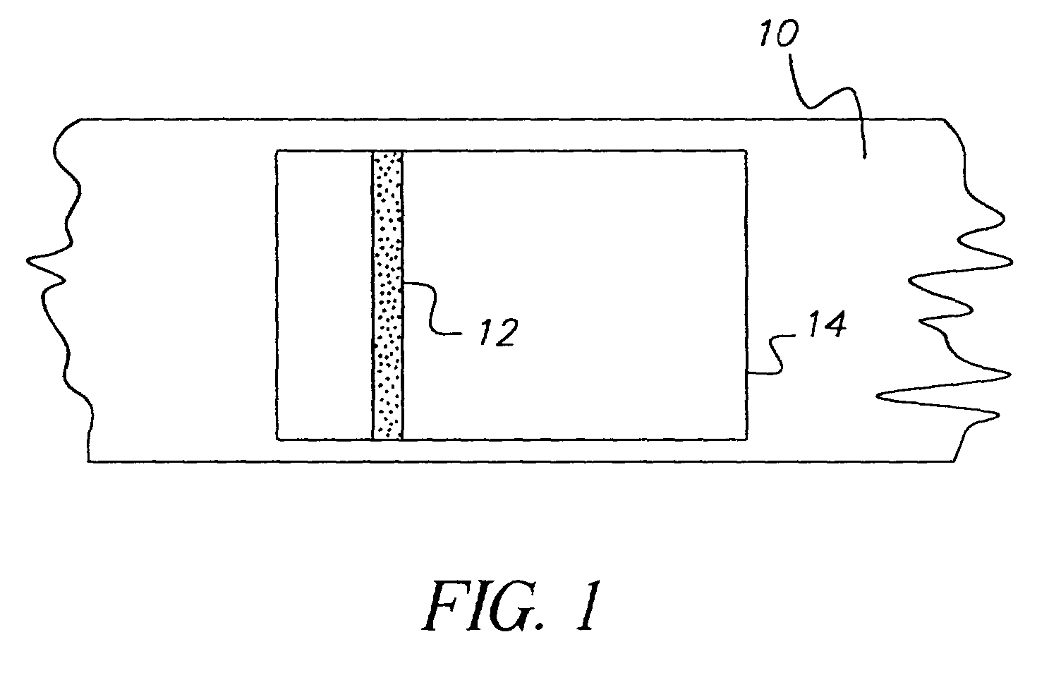
- a reference image of sufficiently uniform exposure 12 is exposed onto a photographic film strip 10 so that the reference image spans the width of an image frame 14 .
- the exposure level is chosen to be high enough that all layers of the film are actively involved in producing density upon development of the latent image formed by the exposure.
- the exposure level is chosen low enough that additional density due to such sources is visible above the overall density of the reference image.
- Advantix 200 film manufactured by Eastman Kodak Company, Rochester, New York an appropriate exposure is adequate to produce a density of 1.5 above Dmin.
- the exposure is high enough to produce a latent image that is developable in all layers of the film and low enough to produce a latent image that upon development allows detection of any additional density due to a defect.
- any multilayer negative film including for example, any multilayer monochrome film.
- a uniform exposure 12 is first exposed ( 20 ) onto a photographic film strip to record a latent image.
- the film strip is next processed ( 22 ) to produce a density signal from the recorded latent image.
- a sampled image is generated ( 24 ) through photometric measurements, preferably by scanning the developed image with a film scanner and digitizing the output of the scanner.
- the sampled image is then analyzed ( 26 ) in order to determine if there are any regions where the uniformity differs from that of the uniform exposure 12. If any such regions are found that are aligned with the length of the film strip, a linear defect has been located ( 28 ).
- a widthwise scan 34 of a digital image of the image frame 14 through the uniform exposure 12 is analyzed by observing the values 36 at each pixel. If a few values 38 differ significantly from the rest of the values 36 in other areas of the scan, a defect has been detected. If multiple scans through the uniform exposure 12 exhibit a defect in the same widthwise location, the defect is located and categorized as a linear defect. Multiple scan lines can be averaged and a similar process applied to the averaged scan lines to enhance the detectability of a linear defect.
- the location can be used in image analysis software to improve the appearance of an image, or in the case of a reference calibration image to improve the reliability of the calibration data.
Abstract
Description
- The present invention relates to photography and more particularly to extended linear defect location on a photographic element in digital photofinishing applications.
- Extended linear defects in scanned renditions of images on photographic elements, such as film, commonly occur. Such defects include, but are not limited to scratches, digs, processing draglines, coating streakiness, coating waviness, scanner defects, etc. For example, during the manufacture of photographic elements, defects in the coating process can lead to narrow regions, referred to as streaks, along the length of the photographic element in which one or more of the light-sensitive layers are affected. Because of the affected layer or layers, there is a change in the amount of light-sensitive material and/or coupler in the streak region. This manifests itself in abnormal characteristic data in the streak region. In a second example, a dirt particle in a camera can lead to a developable latent image formed by pressure sensitization when film is transported over the dust particle which is manifested as an extended linear defect.
- The use of reference calibration patches exposed on a roll of film to enable better exposure control during optical printing is known in the art. See for example U.S. Patent No. 5,767,983 issued June 16, 1998 to Terashita. The use of reference calibration patches has also been shown to be useful in determining correction values for scanned film data used in digital printing. See for example U.S. Patent No. 5,667,944 issued September 16, 1997 to Reem et al.; and U.S. Patent No. 5,649,260 issued July 15, 1997 to Wheeler et al.
- Although extended linear defects can lead to undesirable artifacts in images of scenes, the effects of such defects when they occur in reference calibration images containing sensitometrically exposed patches can be even more detrimental. If such defects can be detected and located, the location of the image defect can be fed into software intended to measure sensitometric patches, enabling such software to avoid using data derived from the defective region or apply appropriate reconstruction techniques to recover affected data.
- In the prior art, U.S. Patent No. 5,736,996 issued April 7, 1998 to Takada et. al., and U.S. Patent No. 5,189,521 issued February 23, 1993 to Ohtsubo et. al., describe methods of automatically detecting image nonuniformities by laying down a test target on a recording medium. However, the nonuniformites of interest are inherent to a recording head and not the presumably uniform medium onto which the image is recorded. Once a nonuniformity is detected, the recording head is automatically calibrated to deliver uniform densities to the recording medium despite nonuniformities in the recording head. This prior art fails to repair the nonuniformity when such defects arise in the recording medium rather than the recording device or occur after the recording step, as the location and severity of the defects in the medium cannot be determined at the time of printing reference calibration targets.
- Standard techniques for locating linear objects in digitized images, illustratively image segmentation and description techniques as described in Digital Image Processing by Rafael Gonzalez and Paul Wintz, Addison-Wesley Publishing Company, Reading, MA, 1977, may be applied to locate such defects in a nominally uniform sensitometric patch. However, in patches with exposures which exhibit low signal to noise ratios, such detection algorithms break down. Failure to detect a defect in such a patch could lead to bias in estimates of density or noise levels in the patch. Use of corrupted data in a calibration procedure could affect entire images in a deleterious fashion. Further, in highly structured nonuniform images such as two-dimensional barcodes, these standard techniques fail to reliably distinguish between linear features that are part of the barcode and those that arise from an artifact.
- Accordingly there is a need for an improved method to detect and locate linear defects in scanned images of photographic elements.
- The need is met according to the present invention by providing a method of locating a linear defect on a photographic element, the element having a useful imaging width and the defect aligned with length of the element, that includes the steps of: exposing a region of the element to create a latent image which is substantially uniform across the useful imaging width of the element; developing the latent image to produce a density signal; sampling the density signal with a photometric device; and analyzing the sampled density data for the presence of significant deviations aligned with the length of the element to locate the defect.
- Fig. 1 is a schematic diagram of a film strip comprising a defect detection exposure according to the present invention;
- Fig. 2 is a diagram comprising the steps in a method for defect detection according to the present invention; and
- Fig. 3 is a diagram useful in discussing an analysis step according to the present invention.
-
- According to the present invention, a region spanning the width of a typical exposure region on a photographic element, for example the useful width of a film frame on a film strip, is exposed with a sufficiently uniform exposure.
- A photographic element includes at least a base with a photosensitive layer that is sensitive to light to produce a developable latent image. The photosensitive layer may contain conventional silver halide chemistry, or other photosensitive materials such as thermal or pressure developable chemistries. It can have a transparent base, a reflective base, or a base with a magnetically sensitive coating. The photographic element can be processed through standard chemical processes, including but not limited to Kodak Processes C-41 and its variants, ECN-2, VNF-1, ECP-2 and its variants, D-96, D-97, E-4, E-6, K-14, R-3, and RA-2SM, or RA-4; Fuji Processes CN-16 and its variants, CR-6, CP-43FA, CP-47L, CP-48S, RP-305, RA-4RT; Agfa MSC 100/101/200 Film and Paper Processes, Agfacolor Processes 70, 71, 72 and 94, Agfachrome Processes 44NP and 63; and Konica Processes CNK-4, CPK-2-22, DP, and CRK-2, and Konica ECOJET HQA-N, HQA-F, and HQA-P Processes. The photographic element can be processed using alternate processes such as apparently dry processes that may retain some or all of the developed silver or silver halide in the element or that may include lamination and an appropriate amount of water added to swell the photographic element. Depending upon the design of the photographic element, the photographic element can also be processed using dry processes that may include thermal or high pressure treatment. The processing may also include a combination of apparently dry, dry, and traditional wet processes. Examples of suitable alternate and dry processes include the processes disclosed in: U.S. Serial Nos. 60/211,058 filed June 3, 2000 by Levy et al.; 60/211,446 filed June 3, 2000 by Irving et al.; 60/211,065 filed June 3, 2000 by Irving et al.; 60/211,079 June 3, 2000 by Irving et al.; EP Patent No. 0762201A1 published March 12, 1997, by Ishikawa et al.; EP Patent No. 0926550A1, published December 12, 1998, by Iwai, et al.; U.S. Patent No. 5,832,328 issued November 3, 1998 to Ueda; U.S. Patent No. 5,758,223 issued May 26, 1998 to Kobayashi, et al.; U.S. Patent No. 5,698,382 issued December 16, 1997 to Nakahanada, et al.; U.S. Patent No. 5,519,510 issued May 21, 1996 to Edgar; and U.S. Patent No. 5,988,896 issued November 23, 1999 to Edgar. It is noted that in the processes disclosed by Edgar, development and scanning of the image occur simultaneously. Accordingly, it is the intent of the present invention that any development and scanning steps can be performed simultaneously.
- Once the photographic element has been processed and the sample image digitized, all of the pixel values, or a cross-section spanning the width of the exposure region, are compared. If a small region of pixels parallel to the length of the photographic element exhibits values throughout that differ significantly from values exhibited in the other areas of the uniform exposure region, a linear defect has been located in the corresponding position on the photographic element.
- Referring to Fig. 1, in a preferred embodiment, a reference image of sufficiently
uniform exposure 12 is exposed onto aphotographic film strip 10 so that the reference image spans the width of animage frame 14. - Preferably for detection of coating defects, the exposure level is chosen to be high enough that all layers of the film are actively involved in producing density upon development of the latent image formed by the exposure. Preferably for detecting additional density induced by local pressure variation or scratches, the exposure level is chosen low enough that additional density due to such sources is visible above the overall density of the reference image. For example, for Advantix 200 film manufactured by Eastman Kodak Company, Rochester, New York, an appropriate exposure is adequate to produce a density of 1.5 above Dmin. In this case, where the photographic element is a color negative photographic film having a plurality of layers, the exposure is high enough to produce a latent image that is developable in all layers of the film and low enough to produce a latent image that upon development allows detection of any additional density due to a defect. The same principle applies for any multilayer negative film, including for example, any multilayer monochrome film.
- It may not be possible to choose a single exposure level that satisfies both of the above noted requirements. In such a case, a plurality of exposure levels varying along the length of the film strip can be used.
- Referring to Fig. 2, the steps in the method for locating a longitudinal linear defect are described. A
uniform exposure 12 is first exposed (20) onto a photographic film strip to record a latent image. The film strip is next processed (22) to produce a density signal from the recorded latent image. Then, a sampled image is generated (24) through photometric measurements, preferably by scanning the developed image with a film scanner and digitizing the output of the scanner. The sampled image is then analyzed (26) in order to determine if there are any regions where the uniformity differs from that of theuniform exposure 12. If any such regions are found that are aligned with the length of the film strip, a linear defect has been located (28). - Referring to Fig. 3, a
widthwise scan 34 of a digital image of theimage frame 14 through theuniform exposure 12 is analyzed by observing thevalues 36 at each pixel. If afew values 38 differ significantly from the rest of thevalues 36 in other areas of the scan, a defect has been detected. If multiple scans through theuniform exposure 12 exhibit a defect in the same widthwise location, the defect is located and categorized as a linear defect. Multiple scan lines can be averaged and a similar process applied to the averaged scan lines to enhance the detectability of a linear defect. - When a defect has been located, the location can be used in image analysis software to improve the appearance of an image, or in the case of a reference calibration image to improve the reliability of the calibration data.
Claims (9)
- A photographic element having a useful imaging width, the element including a latent image which is substantially uniform across the useful imaging width of the element for use in locating a linear defect aligned with the length of the element.
- The photographic element claimed in claim 1, wherein the photographic element is a negative photographic film having a plurality of layers and the exposure is high enough to produce a latent image that is developable in all layers of the film.
- The photographic element claimed in claim 1, wherein the photographic element is a negative photographic film and the exposure is low enough to produce a latent image that upon development allows detection of any additional density due to a defect.
- The photographic element claimed in claim 1, wherein the photographic element is a negative photographic film having a plurality of layers and the exposure is high enough to produce a latent image that is developable in all layers of the film and the exposure is low enough to produce a latent image that upon development allows detection of any additional density due to a defect.
- The photographic element claimed in claim 4, wherein the exposure is sufficient to produce a developed image that is 1.5 above Dmin.
- The photographic element claimed in claim 11, wherein the photographic element includes a photosensitive layer that contains conventional silver halide chemistry.
- The photographic element claimed in claim 1, wherein the photographic element includes a photosensitive layer that contains thermal developable chemistry.
- The photographic element claimed in claim 1, wherein the photographic element includes a photosensitive layer that contains pressure developable chemistry.
- The photographic element claimed in claim 1, wherein the photographic element is a film strip.
Applications Claiming Priority (2)
| Application Number | Priority Date | Filing Date | Title |
|---|---|---|---|
| US09/635,178 US7113627B1 (en) | 2000-08-09 | 2000-08-09 | Location of extended linear defects |
| US635178 | 2000-08-09 |
Publications (1)
| Publication Number | Publication Date |
|---|---|
| EP1180897A1 true EP1180897A1 (en) | 2002-02-20 |
Family
ID=24546766
Family Applications (1)
| Application Number | Title | Priority Date | Filing Date |
|---|---|---|---|
| EP01202891A Withdrawn EP1180897A1 (en) | 2000-08-09 | 2001-07-30 | Method of detecting defects in a photographic film |
Country Status (4)
| Country | Link |
|---|---|
| US (1) | US7113627B1 (en) |
| EP (1) | EP1180897A1 (en) |
| JP (1) | JP2002090944A (en) |
| CN (1) | CN1337594A (en) |
Families Citing this family (4)
| Publication number | Priority date | Publication date | Assignee | Title |
|---|---|---|---|---|
| CN100399792C (en) * | 2002-12-05 | 2008-07-02 | 瑞昱半导体股份有限公司 | Method and apparatus for removing slide fastener shaped faintness of boundary image |
| JP4185789B2 (en) * | 2003-03-12 | 2008-11-26 | 株式会社日立ハイテクノロジーズ | Pattern inspection method and apparatus |
| US8150163B2 (en) * | 2006-04-12 | 2012-04-03 | Scanbuy, Inc. | System and method for recovering image detail from multiple image frames in real-time |
| JP2012203279A (en) * | 2011-03-28 | 2012-10-22 | Konica Minolta Business Technologies Inc | Image forming apparatus |
Citations (2)
| Publication number | Priority date | Publication date | Assignee | Title |
|---|---|---|---|---|
| US5649260A (en) * | 1995-06-26 | 1997-07-15 | Eastman Kodak Company | Automated photofinishing apparatus |
| US5767983A (en) * | 1995-03-24 | 1998-06-16 | Fuji Photo Film Co., Ltd. | Color copying apparatus for determining exposure amount from image data of an original image and a reference image |
Family Cites Families (53)
| Publication number | Priority date | Publication date | Assignee | Title |
|---|---|---|---|---|
| US3718074A (en) | 1971-05-13 | 1973-02-27 | R Davis | Color data acquisition camera |
| US4211558A (en) | 1975-07-23 | 1980-07-08 | Konishiroku Photo Industry Co., Ltd. | Color printing method |
| US3970857A (en) * | 1975-08-06 | 1976-07-20 | E. I. Du Pont De Nemours And Company | Apparatus for web defect detection including a web swatch that contains a defect |
| US4170419A (en) * | 1977-02-23 | 1979-10-09 | Camsco, Inc. | Optical web inspection system |
| DE2803380A1 (en) | 1978-01-26 | 1979-08-02 | Agfa Gevaert Ag | DEVICE FOR APPLYING TEST EXPOSURE |
| DE2911566A1 (en) | 1979-03-23 | 1980-10-02 | Agfa Gevaert Ag | METHOD AND DEVICE FOR CALIBRATING A COLOR COPIER |
| US4365882A (en) | 1981-06-29 | 1982-12-28 | Disbrow Lynnford E | Color standard method and apparatus |
| JPS58162038A (en) * | 1982-03-23 | 1983-09-26 | Canon Inc | Pattern defect detection apparatus |
| JPS5983144A (en) | 1982-11-02 | 1984-05-14 | Fuji Photo Film Co Ltd | Method for correcting photometric condition of photographic film |
| US4634850A (en) | 1983-10-12 | 1987-01-06 | Drexler Technology Corporation | Quad density optical data system |
| US4786792A (en) | 1983-10-12 | 1988-11-22 | Drexler Technology Corporation | Transmissively read quad density optical data system |
| US5068799A (en) * | 1985-04-24 | 1991-11-26 | Jarrett Jr Harold M | System and method for detecting flaws in continuous web materials |
| US4884102A (en) | 1985-05-22 | 1989-11-28 | Fuji Photo Film Co., Ltd. | Controlling method for a photographic system |
| US5036405A (en) * | 1986-11-19 | 1991-07-30 | Canon Kabushiki Kaisha | Image amending method |
| US4881095A (en) | 1987-09-11 | 1989-11-14 | Fuji Photo Film Co., Ltd. | Process for developing photographed film and for printing images through developed film |
| US4874936A (en) | 1988-04-08 | 1989-10-17 | United Parcel Service Of America, Inc. | Hexagonal, information encoding article, process and system |
| US4939354A (en) | 1988-05-05 | 1990-07-03 | Datacode International, Inc. | Dynamically variable machine readable binary code and method for reading and producing thereof |
| US5267030A (en) | 1989-12-22 | 1993-11-30 | Eastman Kodak Company | Method and associated apparatus for forming image data metrics which achieve media compatibility for subsequent imaging application |
| EP0665105B1 (en) | 1990-04-13 | 1997-11-26 | Canon Kabushiki Kaisha | Image recording apparatus |
| JP3040433B2 (en) | 1990-06-11 | 2000-05-15 | キヤノン株式会社 | Correction data creation method |
| US5075716A (en) | 1990-11-29 | 1991-12-24 | Eastman Kodak Company | Apparatus and method for precisely exposing radiation sensitive materials |
| US5113081A (en) * | 1990-12-27 | 1992-05-12 | Eastman Kodak Company | Web inspection system and method with exposure, detection and sampling means |
| JPH05204120A (en) * | 1991-02-19 | 1993-08-13 | Seiko Epson Corp | Image forming device |
| US5198907A (en) | 1991-08-23 | 1993-03-30 | Eastman Kodak Company | Method and appratus for automatically locating predefined exposure areas in a scanned image |
| US5440648A (en) * | 1991-11-19 | 1995-08-08 | Dalsa, Inc. | High speed defect detection apparatus having defect detection circuits mounted in the camera housing |
| US5274243A (en) * | 1992-05-29 | 1993-12-28 | Eastman Kodak Company | Cylindrical allumination system for inspection of sheet material |
| CA2093449C (en) | 1992-07-17 | 1997-06-17 | Albert D. Edgar | Electronic film development |
| US5400116A (en) * | 1993-11-03 | 1995-03-21 | Eastman Kodak Company | Apparatus and method for producing gradated exposures on radiation sensitive material |
| US5591956A (en) | 1995-05-15 | 1997-01-07 | Welch Allyn, Inc. | Two dimensional data encoding structure and symbology for use with optical readers |
| FR2721418B1 (en) * | 1994-06-15 | 1996-08-14 | Kodak Pathe | Method and device for counting and characterizing defects on a photographic medium. |
| US5452055A (en) | 1994-07-14 | 1995-09-19 | Eastman Kodak Company | Apparatus and method for making a reference exposure on a leading and/or trailing portion of a filmstrip |
| US5565958A (en) * | 1995-04-13 | 1996-10-15 | Eastman Kodak Company | Linear light source for a film scanner |
| US5832328A (en) | 1995-05-19 | 1998-11-03 | Konica Corporation | Automatic processing machine for a silver halide photograhic light-sensitive material |
| US5758223A (en) | 1995-09-04 | 1998-05-26 | Konica Corporation | Automatic processing machine for silver halide photographic light-sensitive material |
| US5698382A (en) | 1995-09-25 | 1997-12-16 | Konica Corporation | Processing method for silver halide color photographic light-sensitive material |
| US5667944A (en) * | 1995-10-25 | 1997-09-16 | Eastman Kodak Company | Digital process sensitivity correction |
| US5696591A (en) * | 1996-01-05 | 1997-12-09 | Eastman Kodak Company | Apparatus and method for detecting longitudinally oriented flaws in a moving web |
| US5747217A (en) * | 1996-04-03 | 1998-05-05 | Minnesota Mining And Manufacturing Company | Laser-induced mass transfer imaging materials and methods utilizing colorless sublimable compounds |
| DE19636865C1 (en) * | 1996-09-11 | 1998-01-02 | Philips Patentverwaltung | Processing device for detecting inclined scratches in video signals from film scanner |
| US5988896A (en) | 1996-10-26 | 1999-11-23 | Applied Science Fiction, Inc. | Method and apparatus for electronic film development |
| JPH11316448A (en) | 1997-12-22 | 1999-11-16 | Konica Corp | Image information generating method, photographic sensitive material, film unit with lens, image display method and image output method |
| JP3767218B2 (en) | 1997-12-25 | 2006-04-19 | コニカミノルタホールディングス株式会社 | Image information recording method |
| US6396565B1 (en) * | 1998-01-27 | 2002-05-28 | Noritsu Koki Co., Ltd. | Photograph printing device, electronic image input device, film scanner, scratch recognition method, memory medium recording scratch recognition program, and image restoration method |
| ES2151397B1 (en) | 1998-06-03 | 2001-07-01 | Martinez Moreno Julio Fernando | APPLICATION UNIT OF A DOSE OF CHEMICAL AND SIMILAR PRODUCTS. |
| AU7586800A (en) * | 1999-09-16 | 2001-04-17 | Applied Science Fiction, Inc. | Method and system for altering defects in a digital image |
| US6650410B2 (en) * | 2000-03-08 | 2003-11-18 | Fuji Photo Film Co., Ltd. | Apparatus, system and method for checking film for defects |
| GB2361133B (en) * | 2000-04-07 | 2004-04-14 | Snell & Wilcox Ltd | Video signal processing |
| US6284445B1 (en) | 2000-08-09 | 2001-09-04 | Eastman Kodak Company | Reference calibration patch arrangement to minimize exposure and measurement artifacts and maximize robustness to defects |
| US6280914B1 (en) | 2000-08-09 | 2001-08-28 | Eastman Kodak Company | Photographic element with reference calibration data |
| US6456798B1 (en) | 2000-08-09 | 2002-09-24 | Eastman Kodak Company | Barcode and data storage arrangement on a photographic element |
| US6407767B1 (en) | 2000-08-09 | 2002-06-18 | Eastman Kodak Company | Apparatus for exposing sensitometric and bar code data onto photosensitive media |
| KR100811964B1 (en) * | 2000-09-28 | 2008-03-10 | 동경 엘렉트론 주식회사 | Resist pattern forming apparatus and method thereof |
| US6870950B2 (en) * | 2001-03-15 | 2005-03-22 | Agere Systems Inc. | Method for detecting defects in a material and a system for accomplishing the same |
-
2000
- 2000-08-09 US US09/635,178 patent/US7113627B1/en not_active Expired - Fee Related
-
2001
- 2001-07-30 EP EP01202891A patent/EP1180897A1/en not_active Withdrawn
- 2001-08-06 JP JP2001238415A patent/JP2002090944A/en active Pending
- 2001-08-09 CN CN01125205.7A patent/CN1337594A/en active Pending
Patent Citations (2)
| Publication number | Priority date | Publication date | Assignee | Title |
|---|---|---|---|---|
| US5767983A (en) * | 1995-03-24 | 1998-06-16 | Fuji Photo Film Co., Ltd. | Color copying apparatus for determining exposure amount from image data of an original image and a reference image |
| US5649260A (en) * | 1995-06-26 | 1997-07-15 | Eastman Kodak Company | Automated photofinishing apparatus |
Also Published As
| Publication number | Publication date |
|---|---|
| CN1337594A (en) | 2002-02-27 |
| JP2002090944A (en) | 2002-03-27 |
| US7113627B1 (en) | 2006-09-26 |
Similar Documents
| Publication | Publication Date | Title |
|---|---|---|
| US5959720A (en) | Method for color balance determination | |
| US6705777B2 (en) | System and method for digital film development using visible light | |
| JP4005277B2 (en) | Image processing apparatus, method, and recording medium | |
| JP2002281303A (en) | Device, method for processing image and recording medium | |
| US7263240B2 (en) | Method, system, and software for improving signal quality using pyramidal decomposition | |
| US7113627B1 (en) | Location of extended linear defects | |
| US6284445B1 (en) | Reference calibration patch arrangement to minimize exposure and measurement artifacts and maximize robustness to defects | |
| US6280914B1 (en) | Photographic element with reference calibration data | |
| US20010041019A1 (en) | Method, system, and software for signal processing using sheep and shepard artifacts | |
| JP2002118766A (en) | Method and system for correcting underwater image | |
| US7035437B2 (en) | Image reading apparatus | |
| US4551023A (en) | System for recording information on photographic image density and process | |
| JP2000209396A (en) | Picture reading method and picture reader | |
| US7292379B2 (en) | Image reader and image reading method | |
| JPH08304933A (en) | Image size identifying device and means | |
| US5703672A (en) | Method of making a photographic print | |
| JP3775312B2 (en) | Image processing method, image processing program, and computer-readable recording medium recording the program | |
| JP3954144B2 (en) | Image processing method and apparatus | |
| US20020105618A1 (en) | Sprocket-hole banding filter and method of removing the sprocket-hole banding | |
| JP4513006B2 (en) | Emulsion scratch determination method and emulsion scratch determination system | |
| JP3749307B2 (en) | Copy apparatus and copy control method | |
| JPH09127621A (en) | Decision method for quantity of light by taking color balance into consideration | |
| US7254324B2 (en) | Systems and methods for film processing quality control | |
| JPH11220621A (en) | Picture reader | |
| JP2006174349A (en) | Method and processor for image repair |
Legal Events
| Date | Code | Title | Description |
|---|---|---|---|
| PUAI | Public reference made under article 153(3) epc to a published international application that has entered the european phase |
Free format text: ORIGINAL CODE: 0009012 |
|
| AK | Designated contracting states |
Kind code of ref document: A1 Designated state(s): DE GB Kind code of ref document: A1 Designated state(s): AT BE CH CY DE DK ES FI FR GB GR IE IT LI LU MC NL PT SE TR |
|
| AX | Request for extension of the european patent |
Free format text: AL;LT;LV;MK;RO;SI |
|
| 17P | Request for examination filed |
Effective date: 20020617 |
|
| AKX | Designation fees paid |
Free format text: DE GB |
|
| STAA | Information on the status of an ep patent application or granted ep patent |
Free format text: STATUS: THE APPLICATION IS DEEMED TO BE WITHDRAWN |
|
| 18D | Application deemed to be withdrawn |
Effective date: 20060802 |