EP1164708A2 - Long range two way low power communication device - Google Patents
Long range two way low power communication device Download PDFInfo
- Publication number
- EP1164708A2 EP1164708A2 EP01111284A EP01111284A EP1164708A2 EP 1164708 A2 EP1164708 A2 EP 1164708A2 EP 01111284 A EP01111284 A EP 01111284A EP 01111284 A EP01111284 A EP 01111284A EP 1164708 A2 EP1164708 A2 EP 1164708A2
- Authority
- EP
- European Patent Office
- Prior art keywords
- output
- digital
- coupled
- magnitude
- circuit
- Prior art date
- Legal status (The legal status is an assumption and is not a legal conclusion. Google has not performed a legal analysis and makes no representation as to the accuracy of the status listed.)
- Granted
Links
Images


Classifications
-
- B—PERFORMING OPERATIONS; TRANSPORTING
- B60—VEHICLES IN GENERAL
- B60R—VEHICLES, VEHICLE FITTINGS, OR VEHICLE PARTS, NOT OTHERWISE PROVIDED FOR
- B60R25/00—Fittings or systems for preventing or indicating unauthorised use or theft of vehicles
- B60R25/20—Means to switch the anti-theft system on or off
- B60R25/24—Means to switch the anti-theft system on or off using electronic identifiers containing a code not memorised by the user
-
- B—PERFORMING OPERATIONS; TRANSPORTING
- B60—VEHICLES IN GENERAL
- B60R—VEHICLES, VEHICLE FITTINGS, OR VEHICLE PARTS, NOT OTHERWISE PROVIDED FOR
- B60R25/00—Fittings or systems for preventing or indicating unauthorised use or theft of vehicles
- B60R25/01—Fittings or systems for preventing or indicating unauthorised use or theft of vehicles operating on vehicle systems or fittings, e.g. on doors, seats or windscreens
- B60R25/04—Fittings or systems for preventing or indicating unauthorised use or theft of vehicles operating on vehicle systems or fittings, e.g. on doors, seats or windscreens operating on the propulsion system, e.g. engine or drive motor
-
- B—PERFORMING OPERATIONS; TRANSPORTING
- B60—VEHICLES IN GENERAL
- B60R—VEHICLES, VEHICLE FITTINGS, OR VEHICLE PARTS, NOT OTHERWISE PROVIDED FOR
- B60R25/00—Fittings or systems for preventing or indicating unauthorised use or theft of vehicles
- B60R25/20—Means to switch the anti-theft system on or off
- B60R25/209—Remote starting of engine
-
- G—PHYSICS
- G07—CHECKING-DEVICES
- G07C—TIME OR ATTENDANCE REGISTERS; REGISTERING OR INDICATING THE WORKING OF MACHINES; GENERATING RANDOM NUMBERS; VOTING OR LOTTERY APPARATUS; ARRANGEMENTS, SYSTEMS OR APPARATUS FOR CHECKING NOT PROVIDED FOR ELSEWHERE
- G07C9/00—Individual registration on entry or exit
- G07C9/00174—Electronically operated locks; Circuits therefor; Nonmechanical keys therefor, e.g. passive or active electrical keys or other data carriers without mechanical keys
- G07C9/00309—Electronically operated locks; Circuits therefor; Nonmechanical keys therefor, e.g. passive or active electrical keys or other data carriers without mechanical keys operated with bidirectional data transmission between data carrier and locks
-
- H—ELECTRICITY
- H04—ELECTRIC COMMUNICATION TECHNIQUE
- H04W—WIRELESS COMMUNICATION NETWORKS
- H04W52/00—Power management, e.g. TPC [Transmission Power Control], power saving or power classes
- H04W52/02—Power saving arrangements
- H04W52/0209—Power saving arrangements in terminal devices
- H04W52/0225—Power saving arrangements in terminal devices using monitoring of external events, e.g. the presence of a signal
- H04W52/0229—Power saving arrangements in terminal devices using monitoring of external events, e.g. the presence of a signal where the received signal is a wanted signal
-
- G—PHYSICS
- G07—CHECKING-DEVICES
- G07C—TIME OR ATTENDANCE REGISTERS; REGISTERING OR INDICATING THE WORKING OF MACHINES; GENERATING RANDOM NUMBERS; VOTING OR LOTTERY APPARATUS; ARRANGEMENTS, SYSTEMS OR APPARATUS FOR CHECKING NOT PROVIDED FOR ELSEWHERE
- G07C9/00—Individual registration on entry or exit
- G07C9/00174—Electronically operated locks; Circuits therefor; Nonmechanical keys therefor, e.g. passive or active electrical keys or other data carriers without mechanical keys
- G07C9/00309—Electronically operated locks; Circuits therefor; Nonmechanical keys therefor, e.g. passive or active electrical keys or other data carriers without mechanical keys operated with bidirectional data transmission between data carrier and locks
- G07C2009/00365—Electronically operated locks; Circuits therefor; Nonmechanical keys therefor, e.g. passive or active electrical keys or other data carriers without mechanical keys operated with bidirectional data transmission between data carrier and locks in combination with a wake-up circuit
- G07C2009/00373—Electronically operated locks; Circuits therefor; Nonmechanical keys therefor, e.g. passive or active electrical keys or other data carriers without mechanical keys operated with bidirectional data transmission between data carrier and locks in combination with a wake-up circuit whereby the wake-up circuit is situated in the lock
-
- Y—GENERAL TAGGING OF NEW TECHNOLOGICAL DEVELOPMENTS; GENERAL TAGGING OF CROSS-SECTIONAL TECHNOLOGIES SPANNING OVER SEVERAL SECTIONS OF THE IPC; TECHNICAL SUBJECTS COVERED BY FORMER USPC CROSS-REFERENCE ART COLLECTIONS [XRACs] AND DIGESTS
- Y02—TECHNOLOGIES OR APPLICATIONS FOR MITIGATION OR ADAPTATION AGAINST CLIMATE CHANGE
- Y02D—CLIMATE CHANGE MITIGATION TECHNOLOGIES IN INFORMATION AND COMMUNICATION TECHNOLOGIES [ICT], I.E. INFORMATION AND COMMUNICATION TECHNOLOGIES AIMING AT THE REDUCTION OF THEIR OWN ENERGY USE
- Y02D30/00—Reducing energy consumption in communication networks
- Y02D30/70—Reducing energy consumption in communication networks in wireless communication networks
Definitions
- This disclosure includes a microfiche appendix of 1 microfiche consisting of a total number of 54 frames.
- the present invention relates to a communications device. More specifically, the present invention relates to a bi-directional communications implementation that may be used to communicate over relatively long distances at low power, for example, in a remote keyless entry system for cars, trucks, and other vehicles.
- RKEs remote keyless entry devices
- the RKEs common to everyday experience are often designed as smallish plastic enclosures (small enough to fit in a pocket or on a keychain) that incorporate electronics for transmitting command signals from the RKE to a vehicle.
- the RKE includes a set of control buttons which, when activated, cause the RKE to transmit the command signals to the vehicle.
- the command signals that the RKE sends depend on the control button pressed and may, for example, instruct the vehicle to perform tasks ranging from locking the doors to activating an alarm. In the past, however, RKEs were limited in several significant ways.
- a first significant limitation was the uni-directional only operation of previous RKEs.
- past RKEs were only able to transmit from the RKE to the vehicle and thus were unable to obtain feedback of any sort from the vehicle.
- the RKE could not receive a transmission from the vehicle indicating that the doors were locked in response to a previously transmitted RKE control signal.
- RKE users typically had to rely on an imperfect sense of hearing to determine whether the vehicle actually locked its doors in response to a lock door command signal.
- Activating the RKE in a noisy environment or beyond the range over which audible mechanical locking sounds might be heard meant that the RKE user could not be certain that the vehicle had actually locked its doors.
- the absence of bi-directional communication meant that previous RKEs could not provide a mechanism by which a user could activate the RKE to query the vehicle for its status. As a result, it was not possible, for example, to check the vehicle status to determine if it had been broken into (for example by checking sensors to determine a window had been smashed). As further examples, the RKE could not query the vehicle to determine whether the doors were locked, the trunk was locked, or the interior lights were on.
- querying the status of the car to determine if it had been broken into would preferably be accomplished as far away from the vehicle as possible.
- a related query to determine whether there was an actual intruder still present in the car would similarly be accomplished as far away from the vehicle as possible.
- Yet another object of the present invention is to reduce the power required to implement a communications system including a bi-directional communication device by allowing a microprocessor to remain in sleep mode until needed.
- Another object of the present invention is to provide a bi-directional communication device that includes a snapshot recorder for storing signal samples for further processing.
- Yet another object of the present invention is to provide a communications system including a bi-direction communication device with microprocessor based frequency, phase, and time resolution.
- the device includes an antenna for transmitting and receiving signals, an analog section coupled to the antenna, and a digital section coupled to the analog section. More specifically, the analog section includes an intermediate frequency downconverter, a digital Inphase output, and a digital Quadrature phase output.
- the digital section includes an I/Q derotater producing an I output and a Q output, a wakeup detector including a magnitude output, and a threshold comparison circuit coupled to the magnitude output.
- the threshold comparison circuit stores a threshold value indicative of a wakeup signal reception condition, as reflected in the magnitude output.
- the wakeup detector may also, for example, use an accumulator and a moving average circuit between the magnitude output and the threshold comparison circuit.
- the magnitude output itself is typically generated using a magnitude circuit that preferably outputs a magnitude approximation formed by the greater of two inputs plus one half the smaller of the two inputs.
- the two inputs may be, for example, derotated I/Q data, inner/outer products of I/Q data, or correlated inner/outer products.
- the digital section includes an inner/outer product circuit coupled to the I output and the Q output, and I and Q accumulators for the inner and outer products. Correlators for the inner and outer products may also be included (particularly if modulated wakeup signals are expected).
- a snapshot memory is preferably provided and coupled to the I accumulator and the Q accumulator.
- the frequency of the incoming wakeup signal may be determined, as explained in more detail below, by later processing the saved samples.
- a larger snapshot recorder is also included and is used to store the I output and the Q output produced by the derotater. The stored I and Q outputs may then be subsequently processed to determine frequency and information content.
- the analog section typically uses an Inphase analog to digital converter coupled to the intermediate frequency downconverter to produce the digital Inphase output.
- a Quadrature phase analog to digital converter is coupled to the intermediate frequency downconverter and produces the digital Quadrature phase output.
- the analog to digital converters are preferably 1-bit analog to digital converters.
- FIG. 1 that figure shows a communications system 100 including a long range bi-directional communication device 102 ("BCD 102") shown implemented in a single Application Specific Integrated Circuit (ASIC), a crystal oscillator 104, a DC to DC converter 106 and a microprocessor 108.
- the crystal oscillator 104 provides the clock frequency used by the BCD 102 for analog signal processing and to generate internal clocks for digital control.
- the BCD 102 receives power from the DC to DC converter 106 which, in one embodiment, reduces a +12V DC input to a +3V DC output.
- the microprocessor 108 is connected to the BCD 102 for processing which will be explained in detail below.
- the microprocessor 108 may also be connected to support circuitry, including, for example, a coding/decoding chip 110.
- the coding/decoding chip 110 may implement computationally intensive operations such as signal error coding and decoding, encryption and decryption, and the like. Alternatively, the coding/decoding chip 110 may be omitted and the necessary functions implemented in software stored in the memory 122 and executed by the microprocessor 108.
- the microprocessor 108 supports a general purpose data bus 112, which may be used to communicated with external memory, I/O devices, and the like.
- a transmit and receive antenna 114 is included and connected to the BCD 102.
- the BCD 102 may, for example, be implemented in a single Application Specific Integrated Circuit (ASIC). Alternatively, the analog section and digital sections (described below) may be broken into separate ASICs, or both sections may be implemented with discrete circuitry. As will be explained in more detail below, the BCD 102 may alert the microprocessor 108 when incoming communications are detected.
- ASIC Application Specific Integrated Circuit
- the communication system 100 shown in Figure 1 may be integrated into a vehicle, for example.
- the data bus 112 may then be connected to the general purpose data bus routed around to the electronics in the vehicle, including the door locks, trunk lock, security system and the like.
- an associated RKE may incorporate its own communications system 100 to transmit and receive signals to and from the vehicle.
- the data bus 112 in the RKE may be connected to a switch matrix, for example, providing actuable buttons for instructing the vehicle to perform various tasks including locking/unlocking doors, activating alarms, and starting the engine.
- the BCD 102 includes a number of individual signal processing blocks (described in detail below).
- the signal processing blocks may generally be segmented between RF/IF (analog) processing functions 116, 118 and digital processing functions 120.
- RF/IF processing functions 118 for the transmit direction include an I/Q upconversion and transmitter gain.
- the RF/IF processing functions 116 for the receive direction include receiver gain, I/Q downconversion, baseband gain, and analog to digital conversion.
- the digital processing functions 120 include a numerically controlled oscillator (NCO) driven digital I/Q derotator, a wakeup detector and a snapshot recorder.
- NCO numerically controlled oscillator
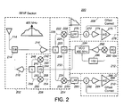
- FIG. 2 that figure shows a detailed diagram 200 of the RF/IF processing functions 116 and 118 in the analog section.
- the RF/IF processing functions are divided into six blocks in Figure 2: the transmit/receive block 202, the analog I/Q downconverter block 204, the analog I/Q upconverter block 206, the I analog to digital converter block 208, the Q analog to digital converter block 210, and the frequency source block 212. Each of the blocks is discussed in detail below.
- the transmit/receive block 202 includes the antenna 114, the transmit/receive switch 214, the receive amplifier 216, and the transmit amplifier 218.
- the antenna 114 captures or sends electromagnetic signals generated by or processed by the BCD 102. Typical transmit and receive frequencies are in the 300-500 MHz range.
- the transmit/receive switch 214 controls whether the BCD 102 is driving the antenna 114 or reading signals captured by the antenna 114.
- the transmit/receive switch 214 may be implemented, for example, as an analog multiplexer or other switching element (for example, a relay). Alternatively, buffers with output disable control may be used to isolate the transmit path from the receive path.
- the receive amplifier 216 serves to boost the signal captured by the antenna 114 for further processing in the analog I/Q downconverter block 204, while the transmit amplifier 218 serves to boost the signal produced by the I/Q upconverter block 206 and applied to the antenna 114.
- the transmit amplifier 218 may be intelligently controlled by the microprocessor 108 to change its output based on manufacturing tolerances, FCC limits, and the like. For example, during manufacturing, sample lots of the communication devices 100 may be tested, and an appropriate power level code supplied in the memory 122 connected to the microprocessor 108. Each communication device 100 may then operate the transmit amplifier 218 at a preferred level.
- the I/Q downconverter block 204 includes a signal splitter 220, a downconverter I mixer 222 with an downconverter I mixer oscillator input 224, an downconverter I mixer signal input 226, and an analog downconverted I output 228.
- the I/Q downconverter block 204 also includes an downconverter Q mixer 230 with an downconverter Q mixer oscillator input 232, an downconverter Q mixer signal input 234, and an analog downconverted Q output 236.
- An oscillator phase shifter 238 is also provided.
- the structure of the I/Q upconverter block 206 is similar to that of the I/Q downconverter block 204
- the upconverter block 206 includes a signal summer 240, an upconverter I mixer 242 with an upconverter I mixer oscillator input 244, an upconverter I mixer signal input 246, and an analog upconverted I output 248.
- the I/Q upconverter block 206 also includes an upconverter Q mixer 250 with an upconverter Q mixer oscillator input 252, an upconverter Q mixer signal input 254, and an analog upconverted Q output 256.
- An oscillator phase shifter 258 is also provided.
- An analog I low pass filter 270 connects the analog downconverted I output to the I analog to digital converter block 208.
- the I analog to digital converter block 208 itself includes a summer 272, an amplifier 274, and an I analog to digital converter 276 which produces a digital I output 278.
- an analog Q low pass filter 280 connects the analog downconverted Q output to the Q analog to digital converter block 210.
- the Q analog to digital converter block 210 includes a summer 282, an amplifier 284, and an analog to digital converter 286 which produces a digital Q output 288.
- the frequency source block 212 includes the crystal oscillator 104, and a frequency multiplier.
- the frequency multiplier uses a phase locked loop including a phase detector 290, amplifier 292, voltage controlled oscillator (VCO) 294.
- a divider 296 closes the loop between the VCO 294 and phase detector 290.
- the crystal oscillator 104 produces an output signal at a relatively low frequency, for example 12.5 MHz.
- the phase detector 290 produces a difference signal representing the difference in frequency or phase between the output of the crystal oscillator 104 and the divided down output of the VCO 294 as selected by the divider 296. In this example, division is set to 32, though other integer and non-integer values may also be used.
- the difference signal is amplified and applied to the VCO to control its output.
- the frequency multiplier shown in the frequency source block 212 thus generates an output signal with a frequency 32 times greater than the crystal oscillator 104 (i.e., 400 MHz).
- the transmit/receive switch 214 allows received signals captured by the antenna 114 to flow through the amplifier 216 and reach the splitter 220.
- the splitter 220 connects identical copies of the received signal to the downconverter I mixer 222 and the downconverter Q mixer 230.
- the downconverter I mixer oscillator input receives the output of the VCO 294, while the downconverter Q mixer oscillator input receives the output of the VCO 294 shifted by 90 degrees (by the oscillator phase shifter 238).
- the frequency content of the received signals are thereby shifted by the mixers 222 and 230 to a difference frequency (the frequencies in the received signals - the VCO 294 frequency) and a sum frequency (the frequencies in the received signals plus the VCO 294 frequency).
- the mixers 222 and 230 thus produce the I and Q components of the received signals, that when filtered by the I and Q low pass filters 270 and 280 produce analog downconverted I and Q signals at an intermediate frequency. For example, if the frequency content of the received signals is centered around 399.9 MHz and the VCO 294 output is 400.0 MHz, then the difference frequency is 100 KHz (the intermediate frequency), and the sum frequency is 799.9 MHz.
- the I and Q low pass filters 270 and 280 remove the sum frequency.
- the intermediate frequency is offset from DC by a small amount (e.g., 100-200 KHz or more) to prevent DC offsets in the processing components from interfering with the downconverted received signals.
- the I and Q low pass filters 270 and 280 may be replaced with band pass filters with a pass band centered around the intermediate frequency and a bandwidth corresponding to the bandwidth of the signals transmitted and received. Using band pass filters provides the benefit of immediately eliminating DC offsets in the signals.
- the downconverted I and Q outputs of the I and Q low pass filters 270 and 280 are adjusted by the summers 272 and 282 to remove DC offsets (explained in more detail with reference to Figure 3, below), amplified by amplifiers 274 and 284, and converted to digital representation on the digital I and Q outputs 278 and 288 by the I and Q analog to digital converters 276 and 286.
- the I and Q analog to digital converters are preferably 1-bit analog to digital converters, although multi-bit converters are also suitable (as noted below).
- the BCD 102 operates on I and Q components generated according to a modulation scheme used by the microprocessor 108, for example BPSK or QPSK.
- the upconverter I and Q mixers 242 and 250 generate two components of the signal to be transmitted.
- the upconverter I mixer signal input accepts the I component (first converted to analog form) and in conjunction with the VCO 294 output (connected to the upconverter I oscillator input 244) produces one component of the signal to be transmitted.
- the upconverter Q mixer signal input accepts the Q component (first converted to analog form) and in conjunction with the VCO 294 output, shifted by 90 degrees by the shifter 258 and connected to the upconverter Q oscillator input 252, produces the second component of the signal to be transmitted.
- the two components are added by the adder 240, boosted by the amplifier 218, and driven through the antenna 114.
- the combination of the frequency synthesizer 370 (described below) and the VCO 294 output may be adjusted to produce a frequency used for transmission that is different than the frequency used for reception.
- the VCO 294 frequency, during reception may be set to approximately 100 KHz greater than the expected received signal center frequency (which may be, for example, 399.9 MHz).
- the VCO 294 and frequency synthesizer 370 may be set instead to generate the 399.9 MHz center frequency.
- a receiver using a 400.0 MHz oscillator may then generate a 100 KHz intermediate frequency from the transmitted signal.
- the digital section 120 includes I and Q offset correctors 302 and 304, a digital I/Q downconverter 306, and digital I and Q accumulators 308 and 310.
- the digital section 120 further includes a wakeup detector 312, a snapshot recorder 314, and a state machine 316. Also shown is a digital frequency synthesizer 370.
- the I and Q offset correctors 302 and 304 are designed to remove DC components (produced by any of the circuitry shown in Figure 2) in the digital I and Q outputs 278 and 288.
- the I offset corrector 302 uses an accumulator constructed with a register 318, a summer 320, and a digital to analog converter 322.
- the register 318 may, for example, count up when the I analog to digital converter 276 produces a 1 value and may count down when the I analog to digital converter 276 produces a 0 value.
- the digital I output 278 is expected to accumulate to 0 (i.e., equal numbers of 1 and 0 values) when there are no DC offsets present. Any DC offset thus accumulates in the register 318, is converted to an analog offset correction by the digital to analog converter 322, and is subtracted from the downconverted I output of the low pass filter 270 by the summer 272 ( Figure 2).
- the Q offset corrector 304 includes the register 324, the summer 326, and the digital to analog converter 328.
- the Q offset corrector operates in substantially the same manner as previously described with respect to the I offset corrector 302.
- the Q offset corrector 304 thereby removes DC offset from the downconverted Q output of the low pass filter 280 using the summer 282.
- the registers 318 and 324 may, for example, be 10 bits wide.
- the I and Q offset correctors 302 and 304 may be replaced with digital to analog converters connected to the I and Q digital outputs 278 and 288.
- the output of the digital to analog converters may then be connected to analog integrators (formed, for example, from operational amplifiers).
- analog integrators formed, for example, from operational amplifiers.
- the output of the analog integrators are connected to the summers 272 and 282 to remove DC offsets in the I and Q signals.
- the I and Q analog to digital converters 276 and 286 are preferably 1 bit converters.
- the discussion below proceeds with respect to the preferred implementation, but may be modified, for example, to use multi-bit analog to digital converters.
- automatic gain control circuits are preferably included to maintain the input signals within an appropriate range for the converters.
- the digital I/Q downconverter 306 removes the intermediate frequency from the digital I and Q outputs 278 and 288.
- the digital I/Q downconverter 306 includes a 16x2 lookup table 330 and a numerically controlled oscillator (NCO) constructed with a register 332 (which may, for example, be 20 bits wide) and summer 334.
- NCO numerically controlled oscillator
- the downconverter 306 operates under the assumption that the digital I and Q outputs 278 and 288 are carried on a particular intermediate frequency (e.g., 100 KHz). Because the particular intermediate frequency may vary over time, temperature, and signal path conditions, the microprocessor 108 tunes the NCO by adjusting the accumulation value in response to algorithms that determine the actual intermediate frequency.
- a particular intermediate frequency e.g. 100 KHz.
- the two most significant bits of the register 332 are provided as inputs to the 16x2 lookup table 330. Because the register 332 is clocked at a constant frequency, it accumulates (using summer 334) in value and rolls over at a constant frequency. By changing the value added each clock pulse, the register 332 can be tuned to roll over more or less frequently.
- the most significant bit (MSB) of the register 332 thereby provides a programmable frequency output and the most significant n bits provide a representation of the phase angle of the frequency output.
- the two MSBs provided to the 16x2 lookup table provide one of four possible phase angle ranges (quadrants) for the selected intermediate frequency.
- the two MSBs may therefore follow the desired intermediate frequency carrying the digital I and Q values through each of four quadrants.
- the 16x2 lookup table 330 may then be indexed according to the quadrant indicated by the MSBs and the sampled I and Q signal values (which will take on constant known values in each quadrant for each bit pattern depending on the modulation technique used).
- Quadrature Phase Shift Keying for example, IQ values are assigned to represent pairs of bits.
- 00 may use a phase angle of 45 degrees
- 01 may use a phase angle of - 45 degrees
- 10 may use a phase angle of 135 degrees
- 11 may use a phase angle of -135 degrees.
- a transmitted 00 signal value takes the form of approximately 0.7 A Cos(wt) - 0.7 A Sin(wt) or I Cos(wt) - Q Sin(wt), where A is a constant and wt is the carrier frequency.
- the NCO is matched to the intermediate frequency wt to compensate for the variation caused by the Sin and Cos terms.
- Table 1 provides the preferred contents of the lookup table 330: NCO MSB, NCO MSB-1 QN, IN Q-Out I-Out 0000 0 0 0001 0 1 0010 1 0 0011 1 1 0100 1 0 0101 0 0 0110 1 1 0.111 0 1 1000 1 1 1001 1 0 1010 0 1 1011 0 0 1100 0 1 1101 1 1 1110 0 0 1111 1 0
- the digital I and Q accumulators 308 and 310 follow the 16x2 lookup table 330.
- the digital I accumulator 308 includes a register 336 and a summer 338.
- the register 336 thus accumulates I values produced by the 16x2 lookup table 330.
- the digital Q accumulator 310 includes a register 340 and a summer 342 and accumulates Q values.
- the digital I and Q accumulators 308 and 310 may accumulate 45 values each, thereby averaging or low pass filtering the I and Q values present in received signals. After 45 values are accumulated, the value of the I and Q registers 336 and 340 are passed on to the wakeup detector 312.
- the wakeup detector 312 includes I and Q absolute value circuits 344 and 346, a magnitude approximation circuit 348, and an accumulator (formed by register 350 and summer 352). Additionally, a threshold register 354 and summer 356 are provided.
- the I and Q absolute value circuits 344 and 346 ensure that only positive I and Q register 336 and 340 magnitudes (for convenience referred to as RI and RQ below) are passed on to the magnitude approximation circuit 348.
- the I and Q absolute value circuits 344 and 346 may be eliminated and replaced with inner and outer product calculation circuitry 358, and inner and outer product value accumulators 360 and 362.
- Values of A and B are accumulated in accumulators 360 and 362, respectively, and additionally saved in snapshot RAM 364. Future processing on the A and B values saved in the snapshot RAM 364 may include, for example, determination of the frequency of the received signal carrier. The frequency may be approximated by summing ATAN2(A,B) over N A and B values, and dividing the sum by N.
- the magnitude approximation circuit 348 calculates an approximation to the magnitude (M) of RI and RQ (when the absolute value circuits 344 and 346 are used) or the magnitude of A and B (when the inner and outer product calculation circuitry 358 is used).
- Values of M are accumulated in the register 350 using the summer 352.
- the value in the register 350 exceeds the value stored in the threshold register 354 (as determined by the summer 356), a significant likelihood exists that a meaningful signal has been received (the "detection threshold" has been exceeded).
- the state machine 316 is therefore informed that the threshold has been exceeded, and the microprocessor 108 may be woken up if in sleep mode.
- a transmitter initially sends a pure sine wave or cosine wave carrier to the BCD 102 before any modulated information.
- the pure carrier increases the likelihood that the value in register 350 will accumulate to exceed the detection threshold.
- the detection threshold itself may be set using register 354 to provide an acceptable ratio of false alarms and missed messages for any particular application.
- the output of the magnitude approximation circuit 348 is connected to an accumulator 366, which in turn is connected to a moving average calculator 368.
- the accumulator 366 preferably keeps a running total of 100 values, and delivers the total every 100 accumulations to the moving average calculator 368.
- the moving average calculator 368 preferably determines a moving average of the last 10 accumulation values delivered to it by the accumulator 366. The output of the moving average calculator 368 is then compared to determine when the detection threshold have been exceeded.
- the associated registers 336 and 340 accumulate, preferably, 45 samples before passing the register values on to subsequent processing.
- two secondary digital I and Q accumulators may be provided using the same structure as the accumulators 308 and 310 (namely, a register and a summer).
- the secondary digital I and Q accumulators accumulate 15 samples before being reset to 0. After each 15 sample accumulation of I and Q samples, the accumulated values are stored in a snapshot recorder 314.
- the I and Q analog to digital converters 276 and 286 sample at 1.5 MHz and the snapshot recorder stores 2000 I values and 2000 Q values.
- the snapshot recorder 314 therefore stores a new value for I and a new value for Q at a 100 KHz rate (1,500,00 / 15) and thus stores 20 ms worth of received signal (as represented by accumulated I and Q samples). Because transmitted signal bursts (in one embodiment) are anticipated to be approximately 10 ms long, the snapshot recorder 314 stores enough data to allow the microprocessor 108 to recover the received signal regardless of whether the received signal was detected at its beginning or at its end. Furthermore, the NCO in the digital I/Q demodulator 306 is clocked at 1.5 MHz as well, and the two MSBs of the digital I/Q downconverter register 332 represent the four quadrant phase angles of a 100 KHz frequency signal.
- an FM or FSK signal may be used as a wakeup signal (as opposed to the continuous wave (CW) wakeup signal assumed above) to prevent a pure tone interferer from activating the communication device 100.
- a wakeup signal (as opposed to the continuous wave (CW) wakeup signal assumed above) to prevent a pure tone interferer from activating the communication device 100.
- an FSK signal centered at a particular frequency may be varied plus or minus 6 KHz to provide a wakeup signal.
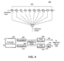
- a correlator such as the one shown in Figure 4 may be used to detect the wakeup signal.
- the correlator 400 shown in Figure 4 uses 10 taps 402 (each preferably representing 1 millisecond of sample time) assigned to the pattern --0++--0++, where a - indicates a first frequency of the FSK signal, a + represents the second frequency, and a 0 represents a transition between the two frequencies zeroed out to eliminate contribution from noise during the transition.
- correlators may be used for the inner product and the outer product.
- the outer correlator 404 follows the accumulator 406 (preferably providing 1 millisecond samples).
- the output 408 of the outer correlator 404 may then be connected to the magnitude approximation circuit 348.
- the inner correlator 410 may follow the accumulator 412.
- the output 414 (after being operated on by the absolute value circuit 416) of the inner correlator 410 may then provided to the magnitude approximation circuit 348.
- the outer product output of the calculation circuitry 358 may be examined for oscillation.
- a suitable detector is shown in Figure 5 and includes the NCO 502, the mixers 504, 506, and the accumulators 508, 510. Also shown are moving average circuits 512, 514, absolute value circuits 520, 522, an I/Q magnitude circuit 516, and a threshold detector 518.
- the outer product output of the calculation circuitry 358 is provided to the two mixers 504, 506.
- the NCO 502 is set to match the expected frequency variation in the output product signal caused by the FSK modulation of the wakeup signal.
- the accumulators 508, 510 and the moving average circuits 512, 514 then accumulate and average the resultant I and Q components and provide their absolute value (using the absolute value circuits 520, 522)them to the magnitude circuit 516.
- the magnitude circuit 516 operates as described above with respect to the magnitude approximation circuit 358.
- the output of the magnitude circuit 516 is then compared to a threshold by the threshold detector 518 to determine if, in fact, a received signal has passed a wakeup threshold.
- the microprocessor 108 may be woken up to process the accumulated I and Q values stored in the snapshot recorder 314. Initially, the microprocessor 108 determines the frequency of the signal stored in the snapshot recorder 314 (for example, by calculating ATAN2(A,B) and averaging, as noted above). The microprocessor then controls the snapshot recorder 314 to capture the next burst (which, in a predefined signaling environment will occur a fixed time later, for example, 90 ms).
- the frequency synthesizer 370 is shown including a lookup table 372, digital to analog converters 374, 376, and low pass filters 378, 380.
- the lookup table 372 accepts (for example) eight bits from the NCO 332 and outputs in response digitized Sine and Cosine values, for example, at six bits of resolution.
- the Sine and Cosine values are converted to analog and low pass filtered.
- the resultant signals are provided to the mixer inputs 246 and 254 as part of the upconversion and data transmission process.
- the NCO 332 may thereby be used to shift the transmit frequency to a desired value and optionally to compensate for a nominal crystal 104 error (or manufacturing tolerances, and the like) by storing these parameters (i.e., a frequency shift code and a frequency correction code) in the memory 122.
- the communication device 100 may also optionally include the ability to communicate at different rates.
- the communication device 100 may transmit first a relatively fast rate (e.g., 10 Kilobytes per second) wakeup signal followed by substantive information to obtain a rapid response from a receiver. If the communication device 100 is too far from the receiver for reliable communication at the fast rate, the receiver will not successfully decode the transmitted signal and generally will not send a response.
- the communication device 100 may then resend at a relatively slower rate (e.g., 1 Kilobyte per second).
- signal sampling in the communication device 100 occurs at some multiple of the data rate (e.g., 10 times the data rate).
- the size of the memory may be increased, or the data rate multiple may be decreased while keeping the same memory size. Alternatively, the number of stored bits per sample may be decreased while keeping the same memory size.
- FIG. 6 that figure illustrates a high level flow diagram 600 encompassing the wakeup detection discussed above.
- the communication device receives an incoming signal.
- the resultant received signal is then downconverted at step 604 and derotated at step 606.
- the derotated I/Q values are accumulated at step 608 in preparation for determination of wakeup conditions.
- the inner and outer products of the derotated I/Q values may be formed.
- the inner and outer products may be used above as described in Figure 3 to detect a continuous wave wakeup signal, or may, in conjunction with the correlation of the inner and outer products (step 612) be used to detect a modulated wakeup signal.
- a magnitude output is produced that is indicative of the presence of a wakeup signal.
- the magnitude output may be formed from the derotated l/Q values, the inner and outer products, or the correlated inner and outer product values, for example.
- the communication device may compare against a predetermined threshold to determine whether a wakeup signal has, in fact, been received.
- the following algorithms presented in the source code appendix provide an implementation of the signal processing undertaken by the processor 108.
- the algorithms include frequency and time of arrival estimation (for a CW burst or a burst containing a BPSK timing reference pattern) as well as demodulation and detection of information bits (for a burst containing random BPSK bits).
- the algorithms are presented as software routines written in Mathcad programming language (with file names ending in .mcd) and C (with file names ending in .c).
- the routines are named and described as follows: Frequency and Time of Arrival Estimation CFT.MCD coarse accuracy frequency and time estimation FF.MCD fine accuracy frequency estimation FFU.MCD fine accuracy frequency estimation in the presence of BPSK bits FTF.MCD fine accuracy timing estimation for the fast data mode FTS.NCD fine accuracy timing estimation for the slow data mode Demodulation and Detection of the Information Bits DMF.MCD BPSK demodulation and detection for the fast data mode DMS.MCD BPSK demodulation and detection for the slow data mode Supporting Constants, Functions, and Tables CONST.MCD basic constants FUNCT.MCD basic functions TABLE.MCD basic tables SUM.MCD summation and derotation functions DERSUM.C "C" source for creating DERSUM.DLL a User defined function add-on to Mathcad to support
- the present bi-directional communication device thus provides a long range, low power communication device with a sophisticated wakeup detector.
- the wakeup detector allows the communication device to save power, yet still reliably receive, decode, and process substantive communication signals sent after a wakeup signal, as well as the wakeup signal itself.
- the snapshot memories provide storage for the wakeup signal, in certain embodiments, as well as the substantive communication signals.
- An associated microprocessor may then examine the contents of the snapshot memories, for example, to perform coarse or fine frequency estimation, or decode and extract useful data.
Abstract
Description
- This disclosure includes a microfiche appendix of 1 microfiche consisting of a total number of 54 frames.
- The present invention relates to a communications device. More specifically, the present invention relates to a bi-directional communications implementation that may be used to communicate over relatively long distances at low power, for example, in a remote keyless entry system for cars, trucks, and other vehicles.
- The automotive industry has for many years turned to the skills of electronics designers, including the Automotive Electronics Group at TRW Inc. for remote keyless entry devices ("RKEs"). The RKEs common to everyday experience are often designed as smallish plastic enclosures (small enough to fit in a pocket or on a keychain) that incorporate electronics for transmitting command signals from the RKE to a vehicle. The RKE includes a set of control buttons which, when activated, cause the RKE to transmit the command signals to the vehicle. The command signals that the RKE sends depend on the control button pressed and may, for example, instruct the vehicle to perform tasks ranging from locking the doors to activating an alarm. In the past, however, RKEs were limited in several significant ways.
- A first significant limitation was the uni-directional only operation of previous RKEs. In other words, past RKEs were only able to transmit from the RKE to the vehicle and thus were unable to obtain feedback of any sort from the vehicle. As an example, the RKE could not receive a transmission from the vehicle indicating that the doors were locked in response to a previously transmitted RKE control signal. Thus, in the past, RKE users typically had to rely on an imperfect sense of hearing to determine whether the vehicle actually locked its doors in response to a lock door command signal. Activating the RKE in a noisy environment or beyond the range over which audible mechanical locking sounds might be heard meant that the RKE user could not be certain that the vehicle had actually locked its doors.
- Furthermore, the absence of bi-directional communication meant that previous RKEs could not provide a mechanism by which a user could activate the RKE to query the vehicle for its status. As a result, it was not possible, for example, to check the vehicle status to determine if it had been broken into (for example by checking sensors to determine a window had been smashed). As further examples, the RKE could not query the vehicle to determine whether the doors were locked, the trunk was locked, or the interior lights were on.
- A second significant limitation of previous RKEs was their relatively short range. Thus, the RKE could not be used beyond a particular range with any certainty that the command signals sent by the RKE would be received by the vehicle. Thus, in conjunction with, for example, an imperfect sense of hearing, it was not always possible to determine whether the car had locked its doors in response to a lock door command signal. Furthermore, even had previous RKEs been able to query the status of the vehicle, the range limitations inherent with the RKEs limited the usefulness of the query in many instances.
- For example, querying the status of the car to determine if it had been broken into would preferably be accomplished as far away from the vehicle as possible. A related query to determine whether there was an actual intruder still present in the car would similarly be accomplished as far away from the vehicle as possible. As another example, in some instances it would be preferable to activate the vehicle's engine or climate control from a greater distance than the relatively short range provided by previous RKEs. A greater activation range may then allow the engine to warm up or allow the vehicle to achieve comfortable climate settings before the user arrived at the vehicle.
- A need has long existed in the industry for a long range bi-directional handheld communications device with applications including remote keyless entry.
- It is an object of the present invention to provide a bi-directional communication device.
- It is another object of the present invention to provide a bi-directional communication device with extended range.
- It is a further object of the present invention to provide a bi-directional communication device that includes a wakeup detector.
- Yet another object of the present invention is to reduce the power required to implement a communications system including a bi-directional communication device by allowing a microprocessor to remain in sleep mode until needed.
- Another object of the present invention is to provide a bi-directional communication device that includes a snapshot recorder for storing signal samples for further processing.
- Yet another object of the present invention is to provide a communications system including a bi-direction communication device with microprocessor based frequency, phase, and time resolution.
- It is a further object of the present invention to provide microprocessor based demodulation, bit detection, and decryption in a communications system using a bi-directional communication device.
- One or more of the foregoing objects is met in whole or in part by the present communications device. The device includes an antenna for transmitting and receiving signals, an analog section coupled to the antenna, and a digital section coupled to the analog section. More specifically, the analog section includes an intermediate frequency downconverter, a digital Inphase output, and a digital Quadrature phase output. The digital section includes an I/Q derotater producing an I output and a Q output, a wakeup detector including a magnitude output, and a threshold comparison circuit coupled to the magnitude output. The threshold comparison circuit stores a threshold value indicative of a wakeup signal reception condition, as reflected in the magnitude output.
- The wakeup detector may also, for example, use an accumulator and a moving average circuit between the magnitude output and the threshold comparison circuit. The magnitude output itself is typically generated using a magnitude circuit that preferably outputs a magnitude approximation formed by the greater of two inputs plus one half the smaller of the two inputs. The two inputs may be, for example, derotated I/Q data, inner/outer products of I/Q data, or correlated inner/outer products. In one implementation of the communication device, the digital section includes an inner/outer product circuit coupled to the I output and the Q output, and I and Q accumulators for the inner and outer products. Correlators for the inner and outer products may also be included (particularly if modulated wakeup signals are expected).
- A snapshot memory is preferably provided and coupled to the I accumulator and the Q accumulator. The frequency of the incoming wakeup signal may be determined, as explained in more detail below, by later processing the saved samples. A larger snapshot recorder is also included and is used to store the I output and the Q output produced by the derotater. The stored I and Q outputs may then be subsequently processed to determine frequency and information content.
- The analog section typically uses an Inphase analog to digital converter coupled to the intermediate frequency downconverter to produce the digital Inphase output. Similarly, a Quadrature phase analog to digital converter is coupled to the intermediate frequency downconverter and produces the digital Quadrature phase output. The analog to digital converters are preferably 1-bit analog to digital converters.
-
- Figure 1 illustrates a block diagram of a long range bi-directional communication device.
- Figure 2 shows a schematic representation of a radio frequency and intermediate frequency portion of a long range bi-directional communication device including receiver and transmitter signal processing.
- Figure 3 illustrates a block diagram of a digital processing section of a long range bi-directional communication device.
- Figure 4 shows an example of correlator circuitry used to detect an FSK wakeup signal.
- Figure 5 illustrates another example of an FSK wakeup signal detector.
- Figure 6 shows a high level flow diagram of a method for waking up a communication device.
-
- Turning now to Figure 1, that figure shows a
communications system 100 including a long range bi-directional communication device 102 ("BCD 102") shown implemented in a single Application Specific Integrated Circuit (ASIC), acrystal oscillator 104, a DC toDC converter 106 and amicroprocessor 108. Thecrystal oscillator 104 provides the clock frequency used by the BCD 102 for analog signal processing and to generate internal clocks for digital control. The BCD 102 receives power from the DC toDC converter 106 which, in one embodiment, reduces a +12V DC input to a +3V DC output. - The
microprocessor 108 is connected to the BCD 102 for processing which will be explained in detail below. Themicroprocessor 108 may also be connected to support circuitry, including, for example, a coding/decoding chip 110. The coding/decoding chip 110 may implement computationally intensive operations such as signal error coding and decoding, encryption and decryption, and the like. Alternatively, the coding/decoding chip 110 may be omitted and the necessary functions implemented in software stored in thememory 122 and executed by themicroprocessor 108. Themicroprocessor 108 supports a generalpurpose data bus 112, which may be used to communicated with external memory, I/O devices, and the like. - Finally, a transmit and receive
antenna 114 is included and connected to theBCD 102. - The
BCD 102 may, for example, be implemented in a single Application Specific Integrated Circuit (ASIC). Alternatively, the analog section and digital sections (described below) may be broken into separate ASICs, or both sections may be implemented with discrete circuitry. As will be explained in more detail below, theBCD 102 may alert themicroprocessor 108 when incoming communications are detected. - The
communication system 100 shown in Figure 1 may be integrated into a vehicle, for example. Thedata bus 112 may then be connected to the general purpose data bus routed around to the electronics in the vehicle, including the door locks, trunk lock, security system and the like. Similarly, an associated RKE may incorporate itsown communications system 100 to transmit and receive signals to and from the vehicle. Thedata bus 112 in the RKE may be connected to a switch matrix, for example, providing actuable buttons for instructing the vehicle to perform various tasks including locking/unlocking doors, activating alarms, and starting the engine. - Referring again to Figure 1, the
BCD 102 includes a number of individual signal processing blocks (described in detail below). The signal processing blocks may generally be segmented between RF/IF (analog) processing functions 116, 118 and digital processing functions 120. Included in the RF/IF processing functions 118 for the transmit direction are an I/Q upconversion and transmitter gain. The RF/IF processing functions 116 for the receive direction include receiver gain, I/Q downconversion, baseband gain, and analog to digital conversion. The digital processing functions 120 include a numerically controlled oscillator (NCO) driven digital I/Q derotator, a wakeup detector and a snapshot recorder. - Turning now to Figure 2, that figure shows a detailed diagram 200 of the RF/IF processing functions 116 and 118 in the analog section. The RF/IF processing functions are divided into six blocks in Figure 2: the transmit/receive
block 202, the analog I/Q downconverter block 204, the analog I/Q upconverter block 206, the I analog to digital converter block 208, the Q analog todigital converter block 210, and thefrequency source block 212. Each of the blocks is discussed in detail below. - The transmit/receive
block 202 includes theantenna 114, the transmit/receiveswitch 214, the receiveamplifier 216, and the transmitamplifier 218. Theantenna 114 captures or sends electromagnetic signals generated by or processed by theBCD 102. Typical transmit and receive frequencies are in the 300-500 MHz range. The transmit/receiveswitch 214 controls whether theBCD 102 is driving theantenna 114 or reading signals captured by theantenna 114. The transmit/receiveswitch 214 may be implemented, for example, as an analog multiplexer or other switching element (for example, a relay). Alternatively, buffers with output disable control may be used to isolate the transmit path from the receive path. The receiveamplifier 216 serves to boost the signal captured by theantenna 114 for further processing in the analog I/Q downconverter block 204, while the transmitamplifier 218 serves to boost the signal produced by the I/Q upconverter block 206 and applied to theantenna 114. - The transmit
amplifier 218 may be intelligently controlled by themicroprocessor 108 to change its output based on manufacturing tolerances, FCC limits, and the like. For example, during manufacturing, sample lots of thecommunication devices 100 may be tested, and an appropriate power level code supplied in thememory 122 connected to themicroprocessor 108. Eachcommunication device 100 may then operate the transmitamplifier 218 at a preferred level. - The I/
Q downconverter block 204 includes asignal splitter 220, adownconverter I mixer 222 with an downconverter Imixer oscillator input 224, an downconverter I mixer signalinput 226, and an analog downconvertedI output 228. The I/Q downconverter block 204 also includes andownconverter Q mixer 230 with an downconverter Qmixer oscillator input 232, an downconverter Qmixer signal input 234, and an analog downconverted Q output 236. Anoscillator phase shifter 238 is also provided. - The structure of the I/
Q upconverter block 206 is similar to that of the I/Q downconverter block 204 Theupconverter block 206 includes asignal summer 240, an upconverter I mixer 242 with an upconverter Imixer oscillator input 244, an upconverter I mixer signalinput 246, and an analog upconvertedI output 248. The I/Q upconverter block 206 also includes anupconverter Q mixer 250 with an upconverter Qmixer oscillator input 252, an upconverter Qmixer signal input 254, and an analogupconverted Q output 256. Anoscillator phase shifter 258 is also provided. - An analog I
low pass filter 270 connects the analog downconverted I output to the I analog to digital converter block 208. The I analog to digital converter block 208 itself includes asummer 272, anamplifier 274, and an I analog todigital converter 276 which produces adigital I output 278. Similarly, an analog Qlow pass filter 280 connects the analog downconverted Q output to the Q analog todigital converter block 210. The Q analog todigital converter block 210 includes asummer 282, anamplifier 284, and an analog todigital converter 286 which produces adigital Q output 288. - The frequency source block 212 includes the
crystal oscillator 104, and a frequency multiplier. The frequency multiplier uses a phase locked loop including aphase detector 290,amplifier 292, voltage controlled oscillator (VCO) 294. Adivider 296 closes the loop between theVCO 294 andphase detector 290. In operation, thecrystal oscillator 104 produces an output signal at a relatively low frequency, for example 12.5 MHz. Thephase detector 290 produces a difference signal representing the difference in frequency or phase between the output of thecrystal oscillator 104 and the divided down output of theVCO 294 as selected by thedivider 296. In this example, division is set to 32, though other integer and non-integer values may also be used. The difference signal is amplified and applied to the VCO to control its output. The frequency multiplier shown in the frequency source block 212 thus generates an output signal with a frequency 32 times greater than the crystal oscillator 104 (i.e., 400 MHz). - Next, the operation of the RF/IF processing components shown in Figure 2 will be described in more detail in the receive direction and the transmit direction. In the receive direction, the transmit/receive
switch 214 allows received signals captured by theantenna 114 to flow through theamplifier 216 and reach thesplitter 220. Thesplitter 220 connects identical copies of the received signal to thedownconverter I mixer 222 and thedownconverter Q mixer 230. The downconverter I mixer oscillator input receives the output of theVCO 294, while the downconverter Q mixer oscillator input receives the output of theVCO 294 shifted by 90 degrees (by the oscillator phase shifter 238). - The frequency content of the received signals are thereby shifted by the
mixers VCO 294 frequency) and a sum frequency (the frequencies in the received signals plus theVCO 294 frequency). Themixers VCO 294 output is 400.0 MHz, then the difference frequency is 100 KHz (the intermediate frequency), and the sum frequency is 799.9 MHz. The I and Q low pass filters 270 and 280 remove the sum frequency. Preferably, the intermediate frequency is offset from DC by a small amount (e.g., 100-200 KHz or more) to prevent DC offsets in the processing components from interfering with the downconverted received signals. Optionally, the I and Q low pass filters 270 and 280 may be replaced with band pass filters with a pass band centered around the intermediate frequency and a bandwidth corresponding to the bandwidth of the signals transmitted and received. Using band pass filters provides the benefit of immediately eliminating DC offsets in the signals. - The downconverted I and Q outputs of the I and Q low pass filters 270 and 280 are adjusted by the
summers amplifiers Q outputs digital converters - In the transmit direction, the
BCD 102 operates on I and Q components generated according to a modulation scheme used by themicroprocessor 108, for example BPSK or QPSK. The upconverter I andQ mixers 242 and 250 generate two components of the signal to be transmitted. The upconverter I mixer signal input accepts the I component (first converted to analog form) and in conjunction with theVCO 294 output (connected to the upconverter I oscillator input 244) produces one component of the signal to be transmitted. The upconverter Q mixer signal input accepts the Q component (first converted to analog form) and in conjunction with theVCO 294 output, shifted by 90 degrees by theshifter 258 and connected to the upconverterQ oscillator input 252, produces the second component of the signal to be transmitted. The two components are added by theadder 240, boosted by theamplifier 218, and driven through theantenna 114. - It is noted that the combination of the frequency synthesizer 370 (described below) and the
VCO 294 output may be adjusted to produce a frequency used for transmission that is different than the frequency used for reception. As an example, theVCO 294 frequency, during reception, may be set to approximately 100 KHz greater than the expected received signal center frequency (which may be, for example, 399.9 MHz). During transmission, theVCO 294 andfrequency synthesizer 370 may be set instead to generate the 399.9 MHz center frequency. A receiver using a 400.0 MHz oscillator may then generate a 100 KHz intermediate frequency from the transmitted signal. - Turning now to Figure 3, a detailed block diagram 300 of the
digital section 120 of theBCD 102 is shown. Thedigital section 120 includes I and Q offsetcorrectors Q downconverter 306, and digital I andQ accumulators digital section 120 further includes awakeup detector 312, asnapshot recorder 314, and astate machine 316. Also shown is adigital frequency synthesizer 370. - The I and Q offset
correctors Q outputs corrector 302 uses an accumulator constructed with aregister 318, asummer 320, and a digital toanalog converter 322. Theregister 318 may, for example, count up when the I analog todigital converter 276 produces a 1 value and may count down when the I analog todigital converter 276 produces a 0 value. Because the I and Q components of the received signal are expected to be periodic in nature (i.e., sine and cosine components), thedigital I output 278 is expected to accumulate to 0 (i.e., equal numbers of 1 and 0 values) when there are no DC offsets present. Any DC offset thus accumulates in theregister 318, is converted to an analog offset correction by the digital toanalog converter 322, and is subtracted from the downconverted I output of thelow pass filter 270 by the summer 272 (Figure 2). - The Q offset
corrector 304 includes theregister 324, thesummer 326, and the digital toanalog converter 328. The Q offset corrector operates in substantially the same manner as previously described with respect to the I offsetcorrector 302. The Q offsetcorrector 304 thereby removes DC offset from the downconverted Q output of thelow pass filter 280 using thesummer 282. Theregisters - In an alternative embodiment, the I and Q offset
correctors digital outputs summers - As noted above, the I and Q analog to
digital converters Q downconverter 306 removes the intermediate frequency from the digital I andQ outputs Q downconverter 306 includes a 16x2 lookup table 330 and a numerically controlled oscillator (NCO) constructed with a register 332 (which may, for example, be 20 bits wide) andsummer 334. Thedownconverter 306 operates under the assumption that the digital I andQ outputs microprocessor 108 tunes the NCO by adjusting the accumulation value in response to algorithms that determine the actual intermediate frequency. - The two most significant bits of the
register 332 are provided as inputs to the 16x2 lookup table 330. Because theregister 332 is clocked at a constant frequency, it accumulates (using summer 334) in value and rolls over at a constant frequency. By changing the value added each clock pulse, theregister 332 can be tuned to roll over more or less frequently. The most significant bit (MSB) of theregister 332 thereby provides a programmable frequency output and the most significant n bits provide a representation of the phase angle of the frequency output. - The two MSBs provided to the 16x2 lookup table provide one of four possible phase angle ranges (quadrants) for the selected intermediate frequency. The two MSBs may therefore follow the desired intermediate frequency carrying the digital I and Q values through each of four quadrants. The 16x2 lookup table 330 may then be indexed according to the quadrant indicated by the MSBs and the sampled I and Q signal values (which will take on constant known values in each quadrant for each bit pattern depending on the modulation technique used).
- In Quadrature Phase Shift Keying (QPSK), for example, IQ values are assigned to represent pairs of bits. Thus, 00 may use a phase angle of 45 degrees, 01 may use a phase angle of - 45 degrees, 10 may use a phase angle of 135 degrees, and 11 may use a phase angle of -135 degrees. A transmitted 00 signal value, for example, takes the form of approximately 0.7 A Cos(wt) - 0.7 A Sin(wt) or I Cos(wt) - Q Sin(wt), where A is a constant and wt is the carrier frequency. Thus, even if 00 is transmitted constantly, the I and Q values will vary over positive and negative values as the Sin and Cos terms pass through each of four quadrants. The NCO is matched to the intermediate frequency wt to compensate for the variation caused by the Sin and Cos terms.
- Table 1, below, provides the preferred contents of the lookup table 330:
NCO MSB, NCO MSB-1 QN, IN Q-Out I-Out 0000 0 0 0001 0 1 0010 1 0 0011 1 1 0100 1 0 0101 0 0 0110 1 1 0.111 0 1 1000 1 1 1001 1 0 1010 0 1 1011 0 0 1100 0 1 1101 1 1 1110 0 0 1111 1 0 - The digital I and
Q accumulators digital Q accumulator 310 includes a register 340 and asummer 342 and accumulates Q values. As an example, the digital I andQ accumulators wakeup detector 312. - The
wakeup detector 312 includes I and Qabsolute value circuits magnitude approximation circuit 348, and an accumulator (formed by register 350 and summer 352). Additionally, a threshold register 354 andsummer 356 are provided. The I and Qabsolute value circuits magnitude approximation circuit 348. - Alternatively, the I and Q
absolute value circuits product calculation circuitry 358, and inner and outerproduct value accumulators 360 and 362. Thecalculation circuitry 358 calculates the inner product (A) of successive I and Q samples as A = I(n) * I(n-1) + Q(n)*Q(n-1), and the outer product (B) as B = I(n)*Q(n-1) - I(n-1)*Q(n). Values of A and B are accumulated inaccumulators 360 and 362, respectively, and additionally saved insnapshot RAM 364. Future processing on the A and B values saved in thesnapshot RAM 364 may include, for example, determination of the frequency of the received signal carrier. The frequency may be approximated by summing ATAN2(A,B) over N A and B values, and dividing the sum by N. - The
magnitude approximation circuit 348 calculates an approximation to the magnitude (M) of RI and RQ (when theabsolute value circuits product calculation circuitry 358 is used). The classic formulation of magnitude is M = SQRT(RI*RI + RQ*RQ) (or M = SQRT(A*A + B*B)). A preferred approximation is M = LARGER(RI, RQ) + 1/2(SMALLER(RI, RQ)) or (M = LARGER(A,B) + 1/2(SMALLER(A,B)). Thus, if RI is larger than RQ (or A is larger than B), then M = RI + 1/2 *RQ (or M = A + 1/2 *B). - Values of M are accumulated in the register 350 using the summer 352. When the value in the register 350 exceeds the value stored in the threshold register 354 (as determined by the summer 356), a significant likelihood exists that a meaningful signal has been received (the "detection threshold" has been exceeded). The
state machine 316 is therefore informed that the threshold has been exceeded, and themicroprocessor 108 may be woken up if in sleep mode. Preferably, a transmitter initially sends a pure sine wave or cosine wave carrier to theBCD 102 before any modulated information. The pure carrier increases the likelihood that the value in register 350 will accumulate to exceed the detection threshold. The detection threshold itself may be set using register 354 to provide an acceptable ratio of false alarms and missed messages for any particular application. - In a preferred embodiment, the output of the
magnitude approximation circuit 348 is connected to anaccumulator 366, which in turn is connected to a movingaverage calculator 368. Theaccumulator 366 preferably keeps a running total of 100 values, and delivers the total every 100 accumulations to the movingaverage calculator 368. The movingaverage calculator 368 preferably determines a moving average of the last 10 accumulation values delivered to it by theaccumulator 366. The output of the movingaverage calculator 368 is then compared to determine when the detection threshold have been exceeded. - As noted above in the discussion of the digital I and
Q accumulators accumulators 308 and 310 (namely, a register and a summer). Preferably, the secondary digital I and Q accumulators accumulate 15 samples before being reset to 0. After each 15 sample accumulation of I and Q samples, the accumulated values are stored in asnapshot recorder 314. - In one embodiment of the present invention, the I and Q analog to
digital converters snapshot recorder 314 therefore stores a new value for I and a new value for Q at a 100 KHz rate (1,500,00 / 15) and thus stores 20 ms worth of received signal (as represented by accumulated I and Q samples). Because transmitted signal bursts (in one embodiment) are anticipated to be approximately 10 ms long, thesnapshot recorder 314 stores enough data to allow themicroprocessor 108 to recover the received signal regardless of whether the received signal was detected at its beginning or at its end. Furthermore, the NCO in the digital I/Q demodulator 306 is clocked at 1.5 MHz as well, and the two MSBs of the digital I/Q downconverter register 332 represent the four quadrant phase angles of a 100 KHz frequency signal. - In an alternative embodiment, an FM or FSK signal may be used as a wakeup signal (as opposed to the continuous wave (CW) wakeup signal assumed above) to prevent a pure tone interferer from activating the
communication device 100. For example, an FSK signal centered at a particular frequency may be varied plus or minus 6 KHz to provide a wakeup signal. With an FSK wakeup signal (alternating between two frequencies), a correlator such as the one shown in Figure 4 may be used to detect the wakeup signal. Thecorrelator 400 shown in Figure 4 uses 10 taps 402 (each preferably representing 1 millisecond of sample time) assigned to the pattern --0++--0++, where a - indicates a first frequency of the FSK signal, a + represents the second frequency, and a 0 represents a transition between the two frequencies zeroed out to eliminate contribution from noise during the transition. - As shown in Figure 4, separate correlators may be used for the inner product and the outer product. The
outer correlator 404, follows the accumulator 406 (preferably providing 1 millisecond samples). Theoutput 408 of theouter correlator 404 may then be connected to themagnitude approximation circuit 348. Similarly, theinner correlator 410 may follow theaccumulator 412. The output 414 (after being operated on by the absolute value circuit 416) of theinner correlator 410 may then provided to themagnitude approximation circuit 348. - As yet another alternative to detecting an FSK wakeup signal, the outer product output of the
calculation circuitry 358 may be examined for oscillation. A suitable detector is shown in Figure 5 and includes theNCO 502, themixers accumulators average circuits Q magnitude circuit 516, and athreshold detector 518. In operation, the outer product output of thecalculation circuitry 358 is provided to the twomixers NCO 502 is set to match the expected frequency variation in the output product signal caused by the FSK modulation of the wakeup signal. - The
accumulators average circuits magnitude circuit 516. Themagnitude circuit 516 operates as described above with respect to themagnitude approximation circuit 358. The output of themagnitude circuit 516 is then compared to a threshold by thethreshold detector 518 to determine if, in fact, a received signal has passed a wakeup threshold. - As noted above, once a received signal has crossed the detection threshold, the
microprocessor 108 may be woken up to process the accumulated I and Q values stored in thesnapshot recorder 314. Initially, themicroprocessor 108 determines the frequency of the signal stored in the snapshot recorder 314 (for example, by calculating ATAN2(A,B) and averaging, as noted above). The microprocessor then controls thesnapshot recorder 314 to capture the next burst (which, in a predefined signaling environment will occur a fixed time later, for example, 90 ms). - Referring still to Figure 3, the
frequency synthesizer 370 is shown including a lookup table 372, digital toanalog converters NCO 332 and outputs in response digitized Sine and Cosine values, for example, at six bits of resolution. The Sine and Cosine values are converted to analog and low pass filtered. The resultant signals are provided to themixer inputs NCO 332 may thereby be used to shift the transmit frequency to a desired value and optionally to compensate for anominal crystal 104 error (or manufacturing tolerances, and the like) by storing these parameters (i.e., a frequency shift code and a frequency correction code) in thememory 122. - The
communication device 100 may also optionally include the ability to communicate at different rates. Thus, for example, thecommunication device 100 may transmit first a relatively fast rate (e.g., 10 Kilobytes per second) wakeup signal followed by substantive information to obtain a rapid response from a receiver. If thecommunication device 100 is too far from the receiver for reliable communication at the fast rate, the receiver will not successfully decode the transmitted signal and generally will not send a response. Thecommunication device 100 may then resend at a relatively slower rate (e.g., 1 Kilobyte per second). Typically, signal sampling in thecommunication device 100 occurs at some multiple of the data rate (e.g., 10 times the data rate). Thus, in adapting thesnapshot recorder 314 for both transmission rates, the size of the memory may be increased, or the data rate multiple may be decreased while keeping the same memory size. Alternatively, the number of stored bits per sample may be decreased while keeping the same memory size. - Turning now to Figure 6, that figure illustrates a high level flow diagram 600 encompassing the wakeup detection discussed above. At
step 602, the communication device receives an incoming signal. The resultant received signal is then downconverted atstep 604 and derotated atstep 606. The derotated I/Q values are accumulated atstep 608 in preparation for determination of wakeup conditions. - At
step 610, for example, the inner and outer products of the derotated I/Q values may be formed. The inner and outer products may be used above as described in Figure 3 to detect a continuous wave wakeup signal, or may, in conjunction with the correlation of the inner and outer products (step 612) be used to detect a modulated wakeup signal. Atstep 614, a magnitude output is produced that is indicative of the presence of a wakeup signal. The magnitude output may be formed from the derotated l/Q values, the inner and outer products, or the correlated inner and outer product values, for example. After accumulation of the magnitudes (step 616), and optionally forming a moving average of the magnitudes (step 618), the communication device may compare against a predetermined threshold to determine whether a wakeup signal has, in fact, been received. - The following algorithms presented in the source code appendix provide an implementation of the signal processing undertaken by the
processor 108. The algorithms include frequency and time of arrival estimation (for a CW burst or a burst containing a BPSK timing reference pattern) as well as demodulation and detection of information bits (for a burst containing random BPSK bits). - The algorithms are presented as software routines written in Mathcad programming language (with file names ending in .mcd) and C (with file names ending in .c). The routines are named and described as follows:
Frequency and Time of Arrival Estimation CFT.MCD coarse accuracy frequency and time estimation FF.MCD fine accuracy frequency estimation FFU.MCD fine accuracy frequency estimation in the presence of BPSK bits FTF.MCD fine accuracy timing estimation for the fast data mode FTS.NCD fine accuracy timing estimation for the slow data mode Demodulation and Detection of the Information Bits DMF.MCD BPSK demodulation and detection for the fast data mode DMS.MCD BPSK demodulation and detection for the slow data mode Supporting Constants, Functions, and Tables CONST.MCD basic constants FUNCT.MCD basic functions TABLE.MCD basic tables SUM.MCD summation and derotation functions DERSUM.C "C" source for creating DERSUM.DLL a User defined function add-on to Mathcad to support SUM.MCD Demonstration Routines F.MCD Demonstration of coordinated frequency estimation, time estimation, and high speed data detection for a short range high speed message structure. S.MCD Demonstration of coordinated frequency estimation, time estimation, and low speed data detection for a longer range lower speed message structure. Support for the Demonstration Routines SNAP2x.MCD generation of sample data to represent the output of the A/D ATODPOST.C "C" source for creating ATODPOST.DLL a User defined functin add-on to Mathcad to support SNAP2X.MCD - The present bi-directional communication device thus provides a long range, low power communication device with a sophisticated wakeup detector. The wakeup detector allows the communication device to save power, yet still reliably receive, decode, and process substantive communication signals sent after a wakeup signal, as well as the wakeup signal itself. The snapshot memories provide storage for the wakeup signal, in certain embodiments, as well as the substantive communication signals. An associated microprocessor may then examine the contents of the snapshot memories, for example, to perform coarse or fine frequency estimation, or decode and extract useful data.
- While particular elements, embodiments and applications of the present invention have been shown and described, it is understood that the invention is not limited thereto since modifications may be made by those skilled in the art, particularly in light of the foregoing teaching. It is therefore contemplated by the appended claims to cover such modifications and incorporate those features which come within the spirit and scope of the invention.
Claims (18)
- A communication device comprising:an antenna for transmitting and receiving signals;an analog section coupled to the antenna, the analog section comprising transmit and receive circuitry coupled to the antenna, the receive circuitry comprising an intermediate frequency downconverter, a digital Inphase output, and a digital Quadrature phase output; anda digital section coupled to the digital Inphase output and the digital Quadrature phase output, the digital section comprising an I/Q derotater including an I output and a Q output, a wakeup detector including a magnitude circuit including a magnitude output and a threshold comparison circuit coupled to the magnitude output, the threshold comparison circuit comparing the magnitude output to a threshold value indicative of a wakeup signal reception condition.
- The communication device of claim 1, wherein the wakeup detector further comprises an accumulator coupled to the magnitude output and the threshold comparison circuit.
- The communication of claim 2, wherein the wakeup detector further comprises a moving average circuit between the accumulator and the threshold comparison circuit.
- The communication device of claim 1, wherein the digital section further comprises:an inner and outer product circuit coupled to the I output and the Q output;an I accumulator coupled between the inner/outer product circuit and the magnitude circuit; anda Q accumulator coupled between the inner/outer product circuit and the magnitude circuit.
- The communication device of claim 1, wherein the digital section further comprises:an inner/outer product circuit coupled to the I output and the Q output;an inner correlator coupled between the inner/outer product circuit and the magnitude circuit; andan outer correlator coupled to an absolute value circuit, the absolute value circuit coupled to the magnitude circuit.
- The communication device of claim 5, further comprising an I accumulator coupled between the inner and outer product circuit and the outer correlator and a Q accumulator coupled between the inner and outer product circuit and the inner correlator.
- The communication device of claim 1, wherein the magnitude output carries a value indicative of a larger of an inphase value and quadrature value plus half of a smaller of the inphase and quadrature value.
- The communication device of claim 1, wherein the analog section further comprises an Inphase analog to digital converter coupled to the intermediate frequency downconverter and the digital Inphase output and a Quadrature phase analog to digital converter coupled to the intermediate frequency downconverter and the digital Quadrature phase output.
- The communication device of claim 1, further comprising:a transmit amplifier coupled to the antenna;an upconverter coupled to the transmit amplifier, the upconverter including an I input and a Q input,a frequency synthesizer coupled to the I input and the Q input; anda numerically controlled oscillator coupled to the frequency synthesizer.
- The communication device of claim 9, further comprising:a microprocessor coupled to the transmit amplifier; anda memory coupled to the microprocessor, the memory including a transmit amplifier power level code.
- The communication device of claim 9, further comprising:a microprocessor coupled to the transmit amplifier; anda memory coupled to the microprocessor, the memory including a frequency shift code for the numerically controlled oscillator.
- The communication device of claim 11, wherein the memory further includes a frequency correction code for the numerically controlled oscillator.
- A method of activating a communication device using a continuous wave or modulated wakeup signal, the method comprising:receiving an incoming signal at an antenna to generate a received signal;downconverting the received signal to produce a digital I output and a digital Q output;derotating the digital I output and the digital Q output to produce derotated I and Q outputs;producing a magnitude output associated with the derotated I and Q outputs; anddetermining when the accumulated magnitude exceeds a predetermined threshold.
- The method of claim 13, wherein the step of producing a magnitude output comprises producing a magnitude output corresponding to a larger of two input values plus half of a smaller of the two input values.
- The method of claim 13, further comprising the step of accumulating the derotated I and Q outputs before the producing step.
- The method of claim 13, further comprising the step of forming an inner product and an outer product of the derotated I and Q outputs, and wherein the step of producing a magnitude output comprises producing a magnitude output corresponding to larger of the inner and output products plus half of smaller of the inner and outer products.
- The method of claim 13, further comprising the steps of:forming an inner product and an outer product of the derotated I and Q outputs; andgenerating correlated inner product and correlated outer product values before the producing step.
- The method of claim 17, further comprising the step of forming the absolute value of the correlated inner product before the producing step.
Applications Claiming Priority (2)
| Application Number | Priority Date | Filing Date | Title |
|---|---|---|---|
| US58521200A | 2000-06-01 | 2000-06-01 | |
| US585212 | 2000-06-01 |
Publications (3)
| Publication Number | Publication Date |
|---|---|
| EP1164708A2 true EP1164708A2 (en) | 2001-12-19 |
| EP1164708A3 EP1164708A3 (en) | 2003-10-22 |
| EP1164708B1 EP1164708B1 (en) | 2005-08-24 |
Family
ID=24340474
Family Applications (1)
| Application Number | Title | Priority Date | Filing Date |
|---|---|---|---|
| EP01111284A Expired - Lifetime EP1164708B1 (en) | 2000-06-01 | 2001-05-16 | Long range two way low power communication device |
Country Status (4)
| Country | Link |
|---|---|
| EP (1) | EP1164708B1 (en) |
| JP (1) | JP3703733B2 (en) |
| KR (1) | KR20010109475A (en) |
| DE (1) | DE60112843T2 (en) |
Cited By (9)
| Publication number | Priority date | Publication date | Assignee | Title |
|---|---|---|---|---|
| EP1304660A2 (en) * | 2001-10-18 | 2003-04-23 | DaimlerChrysler AG | Vehicle security system |
| FR2851382A1 (en) * | 2003-02-14 | 2004-08-20 | Baracoda | Bluetooth functionality providing system for autonomous recorder, has detection output of electronic radio linked to control input of regulator to power Bluetooth communication module upon detection of electromagnetic wave |
| WO2008155422A1 (en) * | 2007-06-21 | 2008-12-24 | Continental Automotive Gmbh | Receiving unit for wireless communication having a peripheral unit |
| WO2009095869A3 (en) * | 2008-02-01 | 2009-12-17 | Nxp B.V. | Power supply control in a wireless receiver |
| DE102009043056A1 (en) * | 2009-09-28 | 2011-03-31 | Marquardt Gmbh | Electronic closing system for use as e.g. door closing system for access authorization of passenger car, has delta-sigma fractional N-phase locked loop synthesizer with quartz crystal for adjusting preset transmission frequency of channel |
| WO2013135380A1 (en) * | 2012-03-16 | 2013-09-19 | Marquardt Gmbh | Locking system, especially for a motor vehicle |
| CN103661268A (en) * | 2013-12-26 | 2014-03-26 | 高丽韵 | Transmitting device of wireless alarm apparatus of car |
| US11910322B2 (en) | 2018-12-13 | 2024-02-20 | Telefonaktiebolaget Lm Ericsson (Publ) | Wakeup receiver and system using frequency shift keying and shifted-frequency retransmission |
| US11943713B2 (en) | 2018-12-13 | 2024-03-26 | Telefonaktiebolaget Lm Ericsson (Publ) | Wakeup receiver and wakeup signal transmission |
Families Citing this family (2)
| Publication number | Priority date | Publication date | Assignee | Title |
|---|---|---|---|---|
| KR100587007B1 (en) | 2004-12-28 | 2006-06-08 | 삼성전기주식회사 | Wake-up system of wireless transceiver |
| KR100835054B1 (en) * | 2006-10-12 | 2008-06-04 | 삼성전기주식회사 | Wake up receiver and method using spreaded codes |
Citations (5)
| Publication number | Priority date | Publication date | Assignee | Title |
|---|---|---|---|---|
| US4825448A (en) * | 1986-08-07 | 1989-04-25 | International Mobile Machines Corporation | Subscriber unit for wireless digital telephone system |
| US5442553A (en) * | 1992-11-16 | 1995-08-15 | Motorola | Wireless motor vehicle diagnostic and software upgrade system |
| WO1999031817A1 (en) * | 1997-12-12 | 1999-06-24 | Thomson Consumer Electronics, Inc. | Receiver with parallel correlator for spread spectrum digital transmission |
| EP0934857A2 (en) * | 1998-02-07 | 1999-08-11 | GRUNDIG Aktiengesellschaft | Activation device for an electronic apparatus |
| EP1096454A2 (en) * | 1999-10-27 | 2001-05-02 | TRW Inc. | Automatic meter reading system |
Family Cites Families (2)
| Publication number | Priority date | Publication date | Assignee | Title |
|---|---|---|---|---|
| JPH11289312A (en) * | 1998-04-01 | 1999-10-19 | Toshiba Tec Corp | Multicarrier radio communication device |
| JP3470602B2 (en) * | 1998-07-13 | 2003-11-25 | 株式会社日立製作所 | Remote keyless entry system |
-
2001
- 2001-04-09 KR KR1020010018677A patent/KR20010109475A/en not_active Application Discontinuation
- 2001-04-19 JP JP2001120548A patent/JP3703733B2/en not_active Expired - Fee Related
- 2001-05-16 EP EP01111284A patent/EP1164708B1/en not_active Expired - Lifetime
- 2001-05-16 DE DE60112843T patent/DE60112843T2/en not_active Expired - Fee Related
Patent Citations (5)
| Publication number | Priority date | Publication date | Assignee | Title |
|---|---|---|---|---|
| US4825448A (en) * | 1986-08-07 | 1989-04-25 | International Mobile Machines Corporation | Subscriber unit for wireless digital telephone system |
| US5442553A (en) * | 1992-11-16 | 1995-08-15 | Motorola | Wireless motor vehicle diagnostic and software upgrade system |
| WO1999031817A1 (en) * | 1997-12-12 | 1999-06-24 | Thomson Consumer Electronics, Inc. | Receiver with parallel correlator for spread spectrum digital transmission |
| EP0934857A2 (en) * | 1998-02-07 | 1999-08-11 | GRUNDIG Aktiengesellschaft | Activation device for an electronic apparatus |
| EP1096454A2 (en) * | 1999-10-27 | 2001-05-02 | TRW Inc. | Automatic meter reading system |
Cited By (14)
| Publication number | Priority date | Publication date | Assignee | Title |
|---|---|---|---|---|
| EP1304660A2 (en) * | 2001-10-18 | 2003-04-23 | DaimlerChrysler AG | Vehicle security system |
| EP1304660A3 (en) * | 2001-10-18 | 2005-04-13 | DaimlerChrysler AG | Vehicle security system |
| FR2851382A1 (en) * | 2003-02-14 | 2004-08-20 | Baracoda | Bluetooth functionality providing system for autonomous recorder, has detection output of electronic radio linked to control input of regulator to power Bluetooth communication module upon detection of electromagnetic wave |
| WO2004075453A2 (en) * | 2003-02-14 | 2004-09-02 | Baracoda | System comprising controlled-supply communication module, radio communication assembly, methods and readers |
| WO2004075453A3 (en) * | 2003-02-14 | 2004-09-30 | Baracoda | System comprising controlled-supply communication module, radio communication assembly, methods and readers |
| WO2008155422A1 (en) * | 2007-06-21 | 2008-12-24 | Continental Automotive Gmbh | Receiving unit for wireless communication having a peripheral unit |
| WO2009095869A3 (en) * | 2008-02-01 | 2009-12-17 | Nxp B.V. | Power supply control in a wireless receiver |
| US9319984B2 (en) | 2008-02-01 | 2016-04-19 | Nxp Semiconductors | Power supply control in a wireless receiver |
| DE102009043056A1 (en) * | 2009-09-28 | 2011-03-31 | Marquardt Gmbh | Electronic closing system for use as e.g. door closing system for access authorization of passenger car, has delta-sigma fractional N-phase locked loop synthesizer with quartz crystal for adjusting preset transmission frequency of channel |
| WO2013135380A1 (en) * | 2012-03-16 | 2013-09-19 | Marquardt Gmbh | Locking system, especially for a motor vehicle |
| CN103661268A (en) * | 2013-12-26 | 2014-03-26 | 高丽韵 | Transmitting device of wireless alarm apparatus of car |
| CN103661268B (en) * | 2013-12-26 | 2017-03-22 | 中山市高朗电子有限公司 | Transmitting device of wireless alarm apparatus of car |
| US11910322B2 (en) | 2018-12-13 | 2024-02-20 | Telefonaktiebolaget Lm Ericsson (Publ) | Wakeup receiver and system using frequency shift keying and shifted-frequency retransmission |
| US11943713B2 (en) | 2018-12-13 | 2024-03-26 | Telefonaktiebolaget Lm Ericsson (Publ) | Wakeup receiver and wakeup signal transmission |
Also Published As
| Publication number | Publication date |
|---|---|
| JP2002042295A (en) | 2002-02-08 |
| JP3703733B2 (en) | 2005-10-05 |
| EP1164708B1 (en) | 2005-08-24 |
| EP1164708A3 (en) | 2003-10-22 |
| DE60112843D1 (en) | 2005-09-29 |
| KR20010109475A (en) | 2001-12-10 |
| DE60112843T2 (en) | 2006-03-09 |
Similar Documents
| Publication | Publication Date | Title |
|---|---|---|
| EP1164708B1 (en) | Long range two way low power communication device | |
| US6803851B1 (en) | Method for carrying out a keyless access authorization check and keyless access authorization check device | |
| US5949827A (en) | Continuous integration digital demodulator for use in a communication device | |
| JP4163582B2 (en) | Digital receiver and wireless communication system | |
| US20050226312A1 (en) | Transceiver device | |
| US20070021082A1 (en) | Vehicle receiver system in which a single receiver circuit is controlled to receive signals transmitted from a plurality of remote devices having respectively different transmission frequencies | |
| US6072404A (en) | Universal garage door opener | |
| US20060003724A1 (en) | System and method for reducing noise in a recording receiver | |
| EP1096454A2 (en) | Automatic meter reading system | |
| US20050083175A1 (en) | Keyless entry receiver | |
| CA2475974A1 (en) | Frequency-timing control loop for wireless communication systems | |
| US7983329B2 (en) | Communication apparatus and method of controlling same | |
| US6757324B2 (en) | Method and apparatus for detecting jamming signal | |
| EP1438803B1 (en) | A method and a device for controlling data extraction from a data stream containing at least one data packet | |
| US20040037365A1 (en) | Remote transmitter system and method | |
| US6831953B2 (en) | Method of, and a radio terminal for, detecting the presence of a 2-FSK signal | |
| US20070139157A1 (en) | On-vehicle radio device | |
| US7711345B2 (en) | Receiving circuit and receiving method | |
| US20030048860A1 (en) | Method and apparatus for symbol independent discriminator correlator automatic frequency control | |
| US11411594B2 (en) | Vehicle trainable transceiver having a programmable oscillator | |
| JPH1023084A (en) | Communication method, communication equipment using the communication method, transmitter, receiver and remote control system | |
| US6639953B1 (en) | Apparatus and method for efficient binary phase shift key data demodulation | |
| JPH1193477A (en) | Lock control device for vehicle | |
| JP2000008669A (en) | Keyless entry receiver | |
| JP2003046400A (en) | Correction method at reception of asynchronous wireless signal and receiver for asynchronous wireless signal |
Legal Events
| Date | Code | Title | Description |
|---|---|---|---|
| PUAI | Public reference made under article 153(3) epc to a published international application that has entered the european phase |
Free format text: ORIGINAL CODE: 0009012 |
|
| AK | Designated contracting states |
Kind code of ref document: A2 Designated state(s): AT BE CH CY DE DK ES FI FR GB GR IE IT LI LU MC NL PT SE TR |
|
| AX | Request for extension of the european patent |
Free format text: AL;LT;LV;MK;RO;SI |
|
| PUAL | Search report despatched |
Free format text: ORIGINAL CODE: 0009013 |
|
| AK | Designated contracting states |
Kind code of ref document: A3 Designated state(s): AT BE CH CY DE DK ES FI FR GB GR IE IT LI LU MC NL PT SE TR |
|
| AX | Request for extension of the european patent |
Extension state: AL LT LV MK RO SI |
|
| RIC1 | Information provided on ipc code assigned before grant |
Ipc: 7G 07C 9/00 B Ipc: 7B 60R 25/00 B Ipc: 7H 04B 1/38 A |
|
| RAP1 | Party data changed (applicant data changed or rights of an application transferred) |
Owner name: TRW AUTOMOTIVE U.S. LLC |
|
| 17P | Request for examination filed |
Effective date: 20040211 |
|
| 17Q | First examination report despatched |
Effective date: 20040319 |
|
| AKX | Designation fees paid |
Designated state(s): DE GB |
|
| GRAP | Despatch of communication of intention to grant a patent |
Free format text: ORIGINAL CODE: EPIDOSNIGR1 |
|
| GRAS | Grant fee paid |
Free format text: ORIGINAL CODE: EPIDOSNIGR3 |
|
| GRAA | (expected) grant |
Free format text: ORIGINAL CODE: 0009210 |
|
| AK | Designated contracting states |
Kind code of ref document: B1 Designated state(s): DE GB |
|
| REG | Reference to a national code |
Ref country code: GB Ref legal event code: FG4D |
|
| REF | Corresponds to: |
Ref document number: 60112843 Country of ref document: DE Date of ref document: 20050929 Kind code of ref document: P |
|
| PLBE | No opposition filed within time limit |
Free format text: ORIGINAL CODE: 0009261 |
|
| STAA | Information on the status of an ep patent application or granted ep patent |
Free format text: STATUS: NO OPPOSITION FILED WITHIN TIME LIMIT |
|
| 26N | No opposition filed |
Effective date: 20060526 |
|
| PGFP | Annual fee paid to national office [announced via postgrant information from national office to epo] |
Ref country code: DE Payment date: 20090514 Year of fee payment: 9 |
|
| PGFP | Annual fee paid to national office [announced via postgrant information from national office to epo] |
Ref country code: GB Payment date: 20090513 Year of fee payment: 9 |
|
| GBPC | Gb: european patent ceased through non-payment of renewal fee |
Effective date: 20100516 |
|
| PG25 | Lapsed in a contracting state [announced via postgrant information from national office to epo] |
Ref country code: DE Free format text: LAPSE BECAUSE OF NON-PAYMENT OF DUE FEES Effective date: 20101201 |
|
| PG25 | Lapsed in a contracting state [announced via postgrant information from national office to epo] |
Ref country code: GB Free format text: LAPSE BECAUSE OF NON-PAYMENT OF DUE FEES Effective date: 20100516 |