EP1154480A2 - Wiring board and semiconductor device including it - Google Patents
Wiring board and semiconductor device including it Download PDFInfo
- Publication number
- EP1154480A2 EP1154480A2 EP01304076A EP01304076A EP1154480A2 EP 1154480 A2 EP1154480 A2 EP 1154480A2 EP 01304076 A EP01304076 A EP 01304076A EP 01304076 A EP01304076 A EP 01304076A EP 1154480 A2 EP1154480 A2 EP 1154480A2
- Authority
- EP
- European Patent Office
- Prior art keywords
- condenser
- layer
- wiring board
- dielectric layer
- metal substrate
- Prior art date
- Legal status (The legal status is an assumption and is not a legal conclusion. Google has not performed a legal analysis and makes no representation as to the accuracy of the status listed.)
- Withdrawn
Links
Images


Classifications
-
- H—ELECTRICITY
- H01—ELECTRIC ELEMENTS
- H01L—SEMICONDUCTOR DEVICES NOT COVERED BY CLASS H10
- H01L23/00—Details of semiconductor or other solid state devices
- H01L23/48—Arrangements for conducting electric current to or from the solid state body in operation, e.g. leads, terminal arrangements ; Selection of materials therefor
- H01L23/488—Arrangements for conducting electric current to or from the solid state body in operation, e.g. leads, terminal arrangements ; Selection of materials therefor consisting of soldered or bonded constructions
- H01L23/498—Leads, i.e. metallisations or lead-frames on insulating substrates, e.g. chip carriers
- H01L23/49822—Multilayer substrates
-
- H—ELECTRICITY
- H01—ELECTRIC ELEMENTS
- H01L—SEMICONDUCTOR DEVICES NOT COVERED BY CLASS H10
- H01L23/00—Details of semiconductor or other solid state devices
- H01L23/58—Structural electrical arrangements for semiconductor devices not otherwise provided for, e.g. in combination with batteries
- H01L23/64—Impedance arrangements
- H01L23/642—Capacitive arrangements
-
- H—ELECTRICITY
- H05—ELECTRIC TECHNIQUES NOT OTHERWISE PROVIDED FOR
- H05K—PRINTED CIRCUITS; CASINGS OR CONSTRUCTIONAL DETAILS OF ELECTRIC APPARATUS; MANUFACTURE OF ASSEMBLAGES OF ELECTRICAL COMPONENTS
- H05K1/00—Printed circuits
- H05K1/16—Printed circuits incorporating printed electric components, e.g. printed resistor, capacitor, inductor
- H05K1/162—Printed circuits incorporating printed electric components, e.g. printed resistor, capacitor, inductor incorporating printed capacitors
-
- H—ELECTRICITY
- H05—ELECTRIC TECHNIQUES NOT OTHERWISE PROVIDED FOR
- H05K—PRINTED CIRCUITS; CASINGS OR CONSTRUCTIONAL DETAILS OF ELECTRIC APPARATUS; MANUFACTURE OF ASSEMBLAGES OF ELECTRICAL COMPONENTS
- H05K3/00—Apparatus or processes for manufacturing printed circuits
- H05K3/44—Manufacturing insulated metal core circuits or other insulated electrically conductive core circuits
- H05K3/445—Manufacturing insulated metal core circuits or other insulated electrically conductive core circuits having insulated holes or insulated via connections through the metal core
-
- H—ELECTRICITY
- H01—ELECTRIC ELEMENTS
- H01L—SEMICONDUCTOR DEVICES NOT COVERED BY CLASS H10
- H01L2224/00—Indexing scheme for arrangements for connecting or disconnecting semiconductor or solid-state bodies and methods related thereto as covered by H01L24/00
- H01L2224/01—Means for bonding being attached to, or being formed on, the surface to be connected, e.g. chip-to-package, die-attach, "first-level" interconnects; Manufacturing methods related thereto
- H01L2224/10—Bump connectors; Manufacturing methods related thereto
- H01L2224/15—Structure, shape, material or disposition of the bump connectors after the connecting process
- H01L2224/16—Structure, shape, material or disposition of the bump connectors after the connecting process of an individual bump connector
-
- H—ELECTRICITY
- H01—ELECTRIC ELEMENTS
- H01L—SEMICONDUCTOR DEVICES NOT COVERED BY CLASS H10
- H01L2924/00—Indexing scheme for arrangements or methods for connecting or disconnecting semiconductor or solid-state bodies as covered by H01L24/00
- H01L2924/01—Chemical elements
- H01L2924/01019—Potassium [K]
-
- H—ELECTRICITY
- H01—ELECTRIC ELEMENTS
- H01L—SEMICONDUCTOR DEVICES NOT COVERED BY CLASS H10
- H01L2924/00—Indexing scheme for arrangements or methods for connecting or disconnecting semiconductor or solid-state bodies as covered by H01L24/00
- H01L2924/01—Chemical elements
- H01L2924/01078—Platinum [Pt]
-
- H—ELECTRICITY
- H01—ELECTRIC ELEMENTS
- H01L—SEMICONDUCTOR DEVICES NOT COVERED BY CLASS H10
- H01L2924/00—Indexing scheme for arrangements or methods for connecting or disconnecting semiconductor or solid-state bodies as covered by H01L24/00
- H01L2924/095—Indexing scheme for arrangements or methods for connecting or disconnecting semiconductor or solid-state bodies as covered by H01L24/00 with a principal constituent of the material being a combination of two or more materials provided in the groups H01L2924/013 - H01L2924/0715
- H01L2924/097—Glass-ceramics, e.g. devitrified glass
- H01L2924/09701—Low temperature co-fired ceramic [LTCC]
-
- H—ELECTRICITY
- H01—ELECTRIC ELEMENTS
- H01L—SEMICONDUCTOR DEVICES NOT COVERED BY CLASS H10
- H01L2924/00—Indexing scheme for arrangements or methods for connecting or disconnecting semiconductor or solid-state bodies as covered by H01L24/00
- H01L2924/15—Details of package parts other than the semiconductor or other solid state devices to be connected
- H01L2924/151—Die mounting substrate
- H01L2924/153—Connection portion
- H01L2924/1531—Connection portion the connection portion being formed only on the surface of the substrate opposite to the die mounting surface
- H01L2924/15311—Connection portion the connection portion being formed only on the surface of the substrate opposite to the die mounting surface being a ball array, e.g. BGA
-
- H—ELECTRICITY
- H01—ELECTRIC ELEMENTS
- H01L—SEMICONDUCTOR DEVICES NOT COVERED BY CLASS H10
- H01L2924/00—Indexing scheme for arrangements or methods for connecting or disconnecting semiconductor or solid-state bodies as covered by H01L24/00
- H01L2924/30—Technical effects
- H01L2924/301—Electrical effects
- H01L2924/3011—Impedance
-
- H—ELECTRICITY
- H05—ELECTRIC TECHNIQUES NOT OTHERWISE PROVIDED FOR
- H05K—PRINTED CIRCUITS; CASINGS OR CONSTRUCTIONAL DETAILS OF ELECTRIC APPARATUS; MANUFACTURE OF ASSEMBLAGES OF ELECTRICAL COMPONENTS
- H05K1/00—Printed circuits
- H05K1/02—Details
- H05K1/03—Use of materials for the substrate
- H05K1/05—Insulated conductive substrates, e.g. insulated metal substrate
- H05K1/053—Insulated conductive substrates, e.g. insulated metal substrate the metal substrate being covered by an inorganic insulating layer
-
- H—ELECTRICITY
- H05—ELECTRIC TECHNIQUES NOT OTHERWISE PROVIDED FOR
- H05K—PRINTED CIRCUITS; CASINGS OR CONSTRUCTIONAL DETAILS OF ELECTRIC APPARATUS; MANUFACTURE OF ASSEMBLAGES OF ELECTRICAL COMPONENTS
- H05K1/00—Printed circuits
- H05K1/02—Details
- H05K1/03—Use of materials for the substrate
- H05K1/05—Insulated conductive substrates, e.g. insulated metal substrate
- H05K1/056—Insulated conductive substrates, e.g. insulated metal substrate the metal substrate being covered by an organic insulating layer
-
- H—ELECTRICITY
- H05—ELECTRIC TECHNIQUES NOT OTHERWISE PROVIDED FOR
- H05K—PRINTED CIRCUITS; CASINGS OR CONSTRUCTIONAL DETAILS OF ELECTRIC APPARATUS; MANUFACTURE OF ASSEMBLAGES OF ELECTRICAL COMPONENTS
- H05K1/00—Printed circuits
- H05K1/02—Details
- H05K1/14—Structural association of two or more printed circuits
- H05K1/141—One or more single auxiliary printed circuits mounted on a main printed circuit, e.g. modules, adapters
-
- H—ELECTRICITY
- H05—ELECTRIC TECHNIQUES NOT OTHERWISE PROVIDED FOR
- H05K—PRINTED CIRCUITS; CASINGS OR CONSTRUCTIONAL DETAILS OF ELECTRIC APPARATUS; MANUFACTURE OF ASSEMBLAGES OF ELECTRICAL COMPONENTS
- H05K2201/00—Indexing scheme relating to printed circuits covered by H05K1/00
- H05K2201/01—Dielectrics
- H05K2201/0137—Materials
- H05K2201/0175—Inorganic, non-metallic layer, e.g. resist or dielectric for printed capacitor
-
- H—ELECTRICITY
- H05—ELECTRIC TECHNIQUES NOT OTHERWISE PROVIDED FOR
- H05K—PRINTED CIRCUITS; CASINGS OR CONSTRUCTIONAL DETAILS OF ELECTRIC APPARATUS; MANUFACTURE OF ASSEMBLAGES OF ELECTRICAL COMPONENTS
- H05K2201/00—Indexing scheme relating to printed circuits covered by H05K1/00
- H05K2201/01—Dielectrics
- H05K2201/0137—Materials
- H05K2201/0179—Thin film deposited insulating layer, e.g. inorganic layer for printed capacitor
-
- H—ELECTRICITY
- H05—ELECTRIC TECHNIQUES NOT OTHERWISE PROVIDED FOR
- H05K—PRINTED CIRCUITS; CASINGS OR CONSTRUCTIONAL DETAILS OF ELECTRIC APPARATUS; MANUFACTURE OF ASSEMBLAGES OF ELECTRICAL COMPONENTS
- H05K2201/00—Indexing scheme relating to printed circuits covered by H05K1/00
- H05K2201/09—Shape and layout
- H05K2201/09209—Shape and layout details of conductors
- H05K2201/095—Conductive through-holes or vias
- H05K2201/09509—Blind vias, i.e. vias having one side closed
-
- H—ELECTRICITY
- H05—ELECTRIC TECHNIQUES NOT OTHERWISE PROVIDED FOR
- H05K—PRINTED CIRCUITS; CASINGS OR CONSTRUCTIONAL DETAILS OF ELECTRIC APPARATUS; MANUFACTURE OF ASSEMBLAGES OF ELECTRICAL COMPONENTS
- H05K2201/00—Indexing scheme relating to printed circuits covered by H05K1/00
- H05K2201/09—Shape and layout
- H05K2201/09209—Shape and layout details of conductors
- H05K2201/095—Conductive through-holes or vias
- H05K2201/09554—Via connected to metal substrate
-
- H—ELECTRICITY
- H05—ELECTRIC TECHNIQUES NOT OTHERWISE PROVIDED FOR
- H05K—PRINTED CIRCUITS; CASINGS OR CONSTRUCTIONAL DETAILS OF ELECTRIC APPARATUS; MANUFACTURE OF ASSEMBLAGES OF ELECTRICAL COMPONENTS
- H05K2201/00—Indexing scheme relating to printed circuits covered by H05K1/00
- H05K2201/09—Shape and layout
- H05K2201/09209—Shape and layout details of conductors
- H05K2201/09654—Shape and layout details of conductors covering at least two types of conductors provided for in H05K2201/09218 - H05K2201/095
- H05K2201/09809—Coaxial layout
-
- H—ELECTRICITY
- H05—ELECTRIC TECHNIQUES NOT OTHERWISE PROVIDED FOR
- H05K—PRINTED CIRCUITS; CASINGS OR CONSTRUCTIONAL DETAILS OF ELECTRIC APPARATUS; MANUFACTURE OF ASSEMBLAGES OF ELECTRICAL COMPONENTS
- H05K2203/00—Indexing scheme relating to apparatus or processes for manufacturing printed circuits covered by H05K3/00
- H05K2203/03—Metal processing
- H05K2203/0315—Oxidising metal
-
- H—ELECTRICITY
- H05—ELECTRIC TECHNIQUES NOT OTHERWISE PROVIDED FOR
- H05K—PRINTED CIRCUITS; CASINGS OR CONSTRUCTIONAL DETAILS OF ELECTRIC APPARATUS; MANUFACTURE OF ASSEMBLAGES OF ELECTRICAL COMPONENTS
- H05K3/00—Apparatus or processes for manufacturing printed circuits
- H05K3/46—Manufacturing multilayer circuits
- H05K3/4602—Manufacturing multilayer circuits characterized by a special circuit board as base or central core whereon additional circuit layers are built or additional circuit boards are laminated
- H05K3/4608—Manufacturing multilayer circuits characterized by a special circuit board as base or central core whereon additional circuit layers are built or additional circuit boards are laminated comprising an electrically conductive base or core
Definitions
- the present invention relates to a multilayer wiring board. More particularly, the present invention relates to a multilayer wiring board inside which a condenser structure is composed and also relates to a method of manufacturing the multilayer wiring board. Further, the present invention relates to a semiconductor device into which the multilayer wiring board is incorporated and also relates to a method of manufacturing the semiconductor device.
- FIG. 6 A multilayer wiring board of the prior art is shown in Fig. 6.
- the multilayer wiring board 201 of the prior art, shown in Fig. 6, includes a core base material 202 made of insulating material such as glass-epoxy resin or ceramics. On both sides of the core base material 202, there are provided a plurality of wiring layers 203, 203, • • • and a plurality of interlayer insulating layers 204, 204, • • • which are alternately laminated on each other.
- the core base material 202 is provided for enhancing the mechanical strength of the entire multilayer wiring board 201 and also for enhancing the workability of the multilayer wiring board 201.
- this core base material 202 there are provided through-holes 202a, 202a, • • • .
- an electric power supply layer for supplying electric power to the semiconductor element 206 to be mounted and a signal layer for inputting and outputting a signal to and from the semiconductor element 206.
- the semiconductor element 206 is mounted via the solder bumps 207.
- a semiconductor device, in which the semiconductor element 206 is mounted on the multilayer wiring board 201, is mounted on a board (not shown) such as a mother board via the solder bumps 205.
- a chip condenser (not shown) for decoupling is mounted on the multilayer wiring board 201 so that fluctuation in electric potential of the electric power supply layer, and the cross talk caused between the signal layers, can be reduced. Both electrodes of this chip condenser are respectively connected with the wiring layers to be decoupled.
- the length of the wiring between the chip condenser and the wiring layer is as short as possible. The reason is that when the length of the wiring between the chip condenser and the wiring layer is long, the impedance is increased, so that it becomes difficult for the chip condenser to accomplish the above object.
- the drive rate of the semiconductor element 206 is increased, the impedance is remarkably increased. Therefore, it becomes impossible to increase the operation rate of the semiconductor device composed of the multilayer wiring board 201 and the semiconductor element 206.
- the chip condenser is embedded in the interlayer insulating layer 204 so that the length of the wiring between the chip condenser and the wiring layer 203 can be reduced.
- the film thickness of the interlayer insulating layer 204 is larger than the thickness of the chip condenser. Therefore, it becomes impossible to reduce the film thickness of the interlayer insulating layer.
- the film thickness of the interlayer insulating layer is large, it is impossible to fulfill the recent requirements that the total thickness of the multilayer wiring board 201 should be reduced so as to provide a semiconductor device of high density. Further, when the film thickness is large, the cost of the interlayer insulating layer 204 is raised. Therefore, the manufacturing cost of the multilayer wiring board 201 is increased.
- the present invention has been accomplished to solve the above problems.
- a multilayer wiring board comprising: a metal substrate as a core; a condenser dielectric layer formed to cover the metal layer; and a condenser electrode metal layer formed to cover the condenser dielectric layer, so that a condenser is defined by the metal substrate, the condenser dielectric layer and the condenser electrode metal layer.
- the multilayer wiring board includes a metallic base material (metal substrate) which composes a core.
- the surface of this metallic base material is covered with a dielectric layer for a condenser. Further, the surface of this dielectric layer for a condenser is covered with a metallic layer for a condenser electrode.
- the metallic base material, the dielectric layer for a condenser and the metallic layer for a condenser electrode compose a condenser. That is, the metallic base material and the metallic layer for a condenser electrode function as both electrode plates of the condenser, and the dielectric layer for a condenser functions as a dielectric member interposed between them.
- the condenser dielectric layer is provided with a first contact hole to communicate with the metal substrate.
- the condenser electrode metal layer is provided with a second contact hole to communicate with the first contact hole, the diameter of the second contact hole being larger than that of the first contact hole.
- An insulating layer is formed on said condenser electrode metal layer and is provided with a via hole to communicate with the metal substrate through the second and first contact holes.
- a metal substrate contact metal layer is formed on an inner wall of the via hole, so that the metal substrate contact metal layer comes into electrical contact with the metal substrate.
- the first contact hole communicating with the metallic base material is formed on the condenser dielectric layer.
- the second contact hole communicating with the first contact hole, the diameter of the second contact hole being larger than that of the first contact hole, is formed on the metallic layer for a condenser electrode.
- the side wall of the second contact hole and the surface of the metallic base material exposed to the bottom of the first contact hole are separate from each other by the peripheral edge section of the first contact hole. Therefore, even when foreign objects such as particles enter the first and the second contact holes, it is difficult for the metallic layer for a condenser and the metallic base material to be short-circuited with each other. Therefore, the reliability of insulation between the metallic layer for a condenser electrode and the metallic base material can be enhanced.
- the condenser dielectric layer is an oxidized layer of a surface of the metal substrate.
- the metal layer is made of aluminum (Al) and the condenser dielectric layer is made of aluminum oxide. Otherwise, the metal layer can be made of titanium (Ti) and the condenser dielectric layer can be made of titanium oxide.
- a method for manufacturing a multiplayer wiring board comprising the steps of forming a dielectric layer on a surface of a metal substrate as a core and forming a condenser electrode metal layer to cover the condenser dielectric layer, so that a condenser is defined by said metal substrate, the condenser dielectric layer and the condenser electrode metal layer.
- a method for manufacturing a multilayer wiring board comprising the following steps of: forming a dielectric layer on a surface of a metal substrate as a core; forming a condenser electrode metal layer to cover the condenser dielectric layer; providing the condenser electrode metal layer with a second contact hole; providing the condenser dielectric layer at an area in the second contact hole with a first contact hole to communicate with the metal substrate, the diameter of the first contact hole being smaller than that of the second contact hole; forming an insulating layer on the condenser electrode metal layer; providing the insulating layer with a via hole to communicate with the metal substrate through the second and first contact holes; and forming a metal substrate contact metal layer on an inner wall of the via hole, so that the metal substrate contact metal layer comes into electrical contact with the metal substrate.
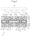
- Fig. 1 is a cross-sectional view showing a multilayer wiring board of an embodiment of the present invention.
- the multilayer wiring board 101 of the embodiment of the present invention is composed in such a manner that a plurality of interlayer insulating layers 105, 105, • • • and a plurality of wiring layers 106, 106, • • • are alternately laminated on each other in an upper and a lower portion of the aluminum base material (metallic base material) 102.
- the aluminum base material (metallic base material) 102 has a function of a core for increasing the mechanical strength of the entire multilayer wiring board 101. This function is the same as the function of the core base material (metal substrate) 202 of the conventional multilayer wiring board 201 shown in Fig. 6. Due to the foregoing, the workability of the multilayer wiring board 101 can be enhanced.
- the interlayer insulating layers 105, 105, • • • are made of, for example, a photosensitive polyimide resin, a non-photosensitive polyimide resin or an epoxy resin.
- On these interlayer insulating layers 105, 105, • • • there are provided via holes 105a, 105a, • • • .
- the wiring layers 106, 106, • • • which are vertically adjacent to each other, are electrically connected with each other.
- the wiring layers 106, 106, • • • are composed in such a manner that non-electrolytic copper plating layers or electrolytic copper plating layers are subjected to patterning.
- the uppermost wiring layer 106a which is one of the wiring layers 106, 106, • • • , there are provided electrode pads 106b, 106b, • • • to which the solder bumps 109, 109, • • • of the semiconductor element 108 to be mounted are attached. Under the condition that the solder bumps 109, 109, • • • are attached to the electrode pads 106b, 106b, • • • , the solder bumps 109, 109, • • • are made to reflow and are then cooled. Due to the foregoing, the semiconductor element 108 and the multilayer wiring board 101 are electrically and mechanically connected with each other.
- solder resist 110 is coated on the uppermost wiring layer 106a, so that the solder bumps 109, 109, • • • , which have been made to reflow, are prevented from spreading to a region except for the electrode pads 106b, 106b, • • • .
- an under-filling agent is made to flow between the semiconductor element 108 and the solder resist 110, it becomes possible to reduce an intensity of stress acting between the semiconductor element 108 and the wiring board 101.
- the electrode pads 106d, 106d, • • • are formed on the lowermost wiring layer 106c.
- the solder bumps 107, 107, • • • are formed on these electrode pads 106d, 106d, • • • .
- solder resist 110 is coated on the lowermost wiring layer 106c, so that the solder bumps 107, 107, •• • , which have been made to reflow, are prevented from spreading to a region except for the electrode pads 106d, 106d, • • • .
- the solder bumps 107, 107, • • • function as the external connection terminals of the multilayer wiring board 101 and electrically and mechanically connect the mother board (not shown) with the multilayer wiring board 101.
- the semiconductor device in which the semiconductor element 108 is mounted on the multilayer wiring board 101, is of the BGA (Ball-Grid-Array) type.
- the present invention is not limited to the above specific embodiment.
- the same action and effect as those explained below can be provided by the semiconductor device of the PGA (Pin-Grid-Array) type in which metallic pins are used instead of the solder bumps 107, 107, • • • .
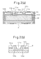
- FIG. 2(a) is an enlarged cross-sectional view showing a primary portion of a multilayer wiring board of an embodiment of the present invention, that is, Fig. 2(a) is a view in which portion A in Fig. 1 is enlarged.
- the thickness of the aluminum base material 102 is approximately 100 to 800 ⁇ m, and the film thickness of the dielectric layer for a condenser is not more than 10 ⁇ m.
- the film thickness of the copper plating layer 104 for a condenser electrode is several ⁇ m to 30 ⁇ m.
- the condenser structure is composed of the aluminum base material 102, the dielectric layer 102a for a condenser and the copper layer 104 for a condenser electrode. That is, the aluminum base material 102 and the copper plating layer 104 for a condenser function as both electrode plates of the condenser, and the dielectric layer 102a for a condenser functions as a dielectric body of the condenser.
- the condenser structure is composed inside the multilayer wiring board 101. Therefore, the length of wiring between the signal lines, which are an object of decoupling, and the condenser can be shortened. Accordingly, even if the operation rate of the semiconductor element 108 is increased, it is possible to suppress an increase in the impedance caused by the length of wiring between the condenser and the signal line. Therefore, the condenser capacitance can be fully utilized. Due to the foregoing, it becomes possible to drive the semiconductor element 108 at a high rate and the occurrence of cross talk between the signal lines on the multilayer wiring board 101 can be suppressed. In this way, the semiconductor device in which the semiconductor element 108 is mounted on the multilayer wiring board 101 can be operated at a high operation rate.
- the condenser is composed inside the multilayer wiring board 101. Therefore, it is unnecessary to embed a chip condenser in the interlayer insulating layer 105 as in the conventional multilayer wiring board. Therefore, it becomes unnecessary that the film thickness of the interlayer insulating layer 105 is increased to be larger than the thickness of the chip condenser. Accordingly, the film thickness of the interlayer insulating layer 105 can be reduced to a predetermined value. Due to the foregoing, the total thickness of the multilayer wiring board 101 can be reduced to be smaller than that of the prior art. For the above reasons, it becomes possible to reduce the size of the semiconductor device in which the semiconductor element 108 is mounted on the multilayer wiring board 101. In addition to that, the film thickness of the interlayer insulating layer 105 can be reduced, so that the manufacturing cost of the interlayer insulating layer 105 can be also reduced. As a result, the manufacturing cost of the multilayer wiring board 101 can be reduced.
- the aluminum base material 102 is used as a core.
- the conventional core base material 202 shown in Fig. 6
- the mechanical strength of the aluminum base material 102 is higher than that of the conventional core base material 202. Therefore, it is possible to reduce the thickness of the aluminum base material 102 to be smaller than the thickness of the core base material 202. Due to the foregoing, the entire thickness of the multilayer wiring board 101 can be reduced to be smaller than that of the prior art.
- the aluminum base material 102 and the copper plating layer 104 for a condenser electrode must be connected with the electric power supply layer, ground layer and signal layer as described before.
- contact holes are formed on the dielectric layer 102a for a condenser and the copper plating layer 104 for a condenser so that the wiring can be laid out from the aluminum base material 102 and the copper plating layer 104 for a condenser electrode.
- the wiring laid out from the aluminum base material 102 will be explained.
- the first contact hole 102b is formed on the dielectric layer 102a for a condenser.
- the second contact hole 104a which is communicated with the first contact hole 102b, is formed on the copper plating layer 104 for a condenser electrode.
- an insulating layer 111 On the copper plating layer 104 for a condenser electrode, there is provided an insulating layer 111. On this insulating layer 111, there is provided a via hole 111a for a metallic base material contact which passes in the second contact hole 104a and the first contact hole 102b and communicates with the aluminum base material 102.
- a copper plating layer 112a for a metallic material base contact comes into electrical contact with the aluminum base material 102 at the bottom of the via hole 111a for a metallic base material contact.
- this copper plating layer 112a for a metallic base material contact is electrically connected with a desired layer on the wiring layers 106, 106, • • • via the via holes 105a (shown in Fig. 1) formed on the interlayer insulating layer 105. Accordingly, the aluminum base material 102 is electrically connected with a desired layer on the wiring layers 206, 206, • • • via the copper plating layer 112a for a metallic base material contact.
- the via hole 111b is formed on the insulating layer 111.
- This via hole 111b is referred to as a via hole 111b for a condenser electrode contact, hereinafter.
- a copper plating layer 112b for a condenser electrode contact On the inner wall of this via hole 111b for a condenser electrode contact, there is provided a copper plating layer 112b for a condenser electrode contact. Therefore, the copper plating layer 112b for a condenser electrode contact is electrically contacted with the copper plating layer 104 for a condenser electrode at the bottom portion of the via hole 111b for a condenser electrode contact.
- This copper plating layer 112b for a condenser electrode contact is electrically connected with a desired layer on the wiring layers 106, 106, • • • via the via hole 105a (shown in Fig. 1) provided on the interlayer insulating layer 105. Accordingly, the copper plating layer 104 for a condenser electrode is electrically connected with a desired layer on the wiring layers 206, 206, • • • via the copper plating layer 112b for a condenser electrode contact.
- wiring is laid from the aluminum base material 102 and the copper plating layer 104 for a condenser electrode to the desired layer on the wiring layers 206, 206, • • • .
- FIG. 2(b) is an enlarged cross-sectional view of portion B in Fig. 2(a). As shown in the drawing, the diameter of the second contact hole 104a is larger than that of the first contact hole 102b.
- the side wall 104b of the second contact hole 104a and the aluminum base material 102d exposed to the bottom portion of the first contact hole 102b are separated from each other by the peripheral edge section 102c of the first contact hole 102b. Accordingly, even if foreign objects such as particles get into the first contact hole 102b and the second contact hole 104a in the manufacturing process of the multilayer wiring board 101, it is difficult for the foreign objects to simultaneously come into contact with both the side wall 104b and the aluminum base material 102d. Therefore, the copper plating layer 104 for a condenser electrode and the aluminum base material 102 are seldom short-circuited with each other. Due to the foregoing, the reliability of the insulation between the layers can be enhanced.
- the condenser composed in the manner described above is used as a condenser for decoupling, however, it should be noted that the present invention is not limited to the above specific embodiment.
- the above condenser can be used as a condenser for adjusting the entire impedance of the multilayer wiring board 101.
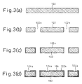
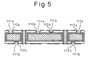
- FIGs. 3(a) to 3(d), 4(a) to 4(d) and 5 are cross-sectional views showing the method of manufacturing the multilayer wiring board of this embodiment.
- the aluminum base material (metal substrate) 102 is prepared.
- the through-holes 102e, 102e, • • • are formed in the aluminum base material 102 by means of wet-etching or punching.
- a plurality of through-holes 102e, 102e, • • • can be simultaneously formed.
- the core base material 202 made of resin or ceramics since the core base material 202 made of resin or ceramics is used, it is impossible to form the through-holes 202a, 202a, • • • by means of wet-etching or punching as in the embodiment of the present invention.
- the through-holes 202a, 202a, • • • are formed by a mechanical drill instead of the means of wet-etching or punching.
- the mechanical drill it is impossible to simultaneously form a plurality of through-holes 202a, 202a, • • • , that is, the through-holes 202a, 202a, • • • must be formed one by one. Accordingly, it takes a long time to form the through-holes.
- the cost of machining conducted by the mechanical drill is higher than that conducted by wet-etching or punching.
- the process shown in Fig. 3(c) is carried out.
- the surface of the aluminum base material 102 is subjected to oxygen-plasma treatment so that the surface layer is oxidized, that is, the surface layer is turned into a dielectric body layer 102a for a condenser made of Al 2 O 3 .
- this oxygen-plasma treatment is not used but powder made of Al 2 O 3 is deposited on the surface of the aluminum base material 102 and fired, the dielectric body layer 102a, for a condenser, made of Al 2 O 3 can be formed.
- the surface of the dielectric layer 102a for a condenser may be coated with resin.
- the film thickness of this dielectric body layer for a condenser is not more than 10 ⁇ m.
- a titanium base material can be used as a metallic base material 102.
- a surface of the titanium (Ti) base material 102 is oxidized to form titanium oxide (TiO 2 ) as a dielectric body layer 102 on the surface of the titanium base material 102.
- the copper plating layer 104 for a condenser electrode On which the second contact holes 104a, 104a, • • • are provided, are formed on the surface of the dielectric layer 102a for a condenser.
- the full-additive method or semi-additive method is used.
- a plating-resist (not shown) is coated at positions corresponding to the second contact holes 104a, 104a • • • on the surface. A portion not coated with this plating-resist is subjected to non-electrolytic copper plating, and then the plating-resist is peeled off. In this way, the copper plating layer 104 for a condenser electrode is completed.
- the semi-additive method after a thin non-electrolytic copper plating layer (not shown) has been formed on the entire surface of the dielectric layer 102a for a condenser, a plating-resist (not shown) is coated at positions corresponding to the second contact holes 104a, 104a ••• on the surface.
- the non-electrolytic copper plating layer which has been formed before, is used as an electric power supply layer, and an electrolytic copper plating layer is formed on the non-electrolytic copper plating layer in a portion not coated with the plating-resist.
- the plating-resist is peeled off, and the non-electrolytic copper plating layer, which has been formed below the plating-resist, is removed by means of etching. In this way, the copper plating layer 104 for a condenser electrode is completed.
- the first contact holes 102b, 102b, • • • are formed on the dielectric body layer 102a for a condenser by means of laser beam machining.
- the diameter of the first contact hole 102b, 102b, • • • is smaller than that of the second contact hole 104b, 104b, • • • .
- the insulating layer 111 is formed on the entire surface.
- this insulating layer 111 is made when a photosensitive polyimide resin, a non-photosensitive polyimide resin or an epoxy resin is coated on the entire surface.
- a resin sheet such as a prepreg sheet may be made to adhere onto the copper plating layer 104 for a condenser electrode so that the insulating layer 111 can be formed.
- the via holes 111a, 111a, • • • for a metallic base material contact, the via holes 111b, 111b, • • • for a condenser electrode contact and the resin through-holes 111c, 111c, • • • are formed on the insulating layer 111 as follows.
- the insulating layer 111 is made of a photosensitive polyimide resin
- these via holes and through-holes are formed when the photosensitive epoxy resin is exposed to light and developed.
- the insulating layer 111 is made of a non-photosensitive resin such as a non-photosensitive polyimide resin, an epoxy resin or a prepreg
- portions in which the via holes and the through-holes are to be formed are irradiated with laser beams so that these portions are removed and the holes are opened.
- the insulating layer 111 may be made by means of electrostatic coating in the process shown in Fig. 4(b).
- the surface profile of the insulating layer 111 becomes substantially the same as that of the base. Therefore, the resin through-holes 111c, 111c, •• • can be smoothly formed corresponding to the through-holes 102e, 102e, • • • .
- the insulating layer 111 is formed by means of electrostatic coating, it becomes unnecessary to provide a process in which the resin through-holes 111c, 111c, • • • are formed. Accordingly, the manufacturing process of the multilayer wiring board 101 can be simplified.
- the resin through-holes 111c, 111c, ••• are filled with the through-hole filling resin 103.
- the copper plating layer 112 is formed in such a manner that the non-electrolytic copper plating layer is formed on the entire surface and then electrolytic copper plating is conducted on the non-electrolytic copper plating layer while the non-electrolytic copper plating layer is being used as an electric power supply layer.
- the through-hole filling resin 103 is filled in the resin through-holes 111c, 111c, • • • by means of screenprinting after the copper plating layer 112 has been formed as described above.
- the copper plating layer 112 is subjected to patterning.
- the copper layers 112 which have been respectively formed on the inner walls of the via holes 111a, 111a, • • • for a metallic base material contact and the via holes 111b, 111b, • • • for a condenser electrode contact, are left and are not removed.
- the copper plating layer 112 left on the inner walls of the via holes 111a, 111a, • • • for a metallic base material contact becomes the copper plating layer 112a for a metallic base material contact.
- the copper plating layer 112 left on the inner walls of the via holes 111b, 111b, • • • for a condenser electrode contact becomes the copper plating layer 112b for a condenser electrode contact.
- the condenser structure composing a primary portion of the multilayer wiring board of the present invention is completed.
- the interlayer insulating layers 105, 105, • • • and the wiring layers 106, 106 • • • are alternately laminated on each other, so that the multilayer wiring board 101 shown in Fig. 1 is completed.
- a condenser is composed inside the multilayer wiring board. Therefore, it is unnecessary that a chip condenser is embedded in the interlayer insulating layer. Accordingly, it is possible to reduce the film thickness of the interlayer insulating layer to be smaller that that of the prior art. Due to the foregoing, the thickness of the entire multilayer wiring board can be reduced to be smaller than that of the prior art.
Abstract
Description
- The present invention relates to a multilayer wiring board. More particularly, the present invention relates to a multilayer wiring board inside which a condenser structure is composed and also relates to a method of manufacturing the multilayer wiring board. Further, the present invention relates to a semiconductor device into which the multilayer wiring board is incorporated and also relates to a method of manufacturing the semiconductor device.
- Recently, the density of electronic equipment has been highly increased. Accordingly, a multilayer wiring board in which a plurality of wiring layers are laminated together has been realized. A multilayer wiring board of the prior art is shown in Fig. 6.
- The
multilayer wiring board 201 of the prior art, shown in Fig. 6, includes acore base material 202 made of insulating material such as glass-epoxy resin or ceramics. On both sides of thecore base material 202, there are provided a plurality ofwiring layers insulating layers core base material 202 is provided for enhancing the mechanical strength of the entiremultilayer wiring board 201 and also for enhancing the workability of themultilayer wiring board 201. - In this
core base material 202, there are provided through-holes 202a, 202a, • • • . On the inner walls of these through-holes 202a, 202a, • • • , there are provided copper plating layers. Due to these copper plating layers, thewiring layers - Although not shown in Fig. 6, among these
wiring layers semiconductor element 206 to be mounted and a signal layer for inputting and outputting a signal to and from thesemiconductor element 206. - On this
multilayer wiring board 201 of the prior art, thesemiconductor element 206 is mounted via thesolder bumps 207. A semiconductor device, in which thesemiconductor element 206 is mounted on themultilayer wiring board 201, is mounted on a board (not shown) such as a mother board via thesolder bumps 205. - In this connection, it is common that a chip condenser (not shown) for decoupling is mounted on the
multilayer wiring board 201 so that fluctuation in electric potential of the electric power supply layer, and the cross talk caused between the signal layers, can be reduced. Both electrodes of this chip condenser are respectively connected with the wiring layers to be decoupled. In this case, it is preferable that the length of the wiring between the chip condenser and the wiring layer is as short as possible. The reason is that when the length of the wiring between the chip condenser and the wiring layer is long, the impedance is increased, so that it becomes difficult for the chip condenser to accomplish the above object. Especially when the drive rate of thesemiconductor element 206 is increased, the impedance is remarkably increased. Therefore, it becomes impossible to increase the operation rate of the semiconductor device composed of themultilayer wiring board 201 and thesemiconductor element 206. - From the above viewpoint, it is conventional practice that the chip condenser is embedded in the
interlayer insulating layer 204 so that the length of the wiring between the chip condenser and thewiring layer 203 can be reduced. - However, when the chip condenser is embedded in the
interlayer insulating layer 204 as described above, it becomes necessary that the film thickness of theinterlayer insulating layer 204 is larger than the thickness of the chip condenser. Therefore, it becomes impossible to reduce the film thickness of the interlayer insulating layer. When the film thickness of the interlayer insulating layer is large, it is impossible to fulfill the recent requirements that the total thickness of themultilayer wiring board 201 should be reduced so as to provide a semiconductor device of high density. Further, when the film thickness is large, the cost of theinterlayer insulating layer 204 is raised. Therefore, the manufacturing cost of themultilayer wiring board 201 is increased. - Further, irregularities corresponding to the profile of the chip condenser are formed on the surface of the
interlayer insulating layer 204. Therefore, it is impossible to manufacture amultilayer wiring board 201, the surface of which is flat. - The present invention has been accomplished to solve the above problems.
- It is an object of the present invention to provide a multilayer wiring board inside which a condenser structure is composed so that it unnecessary to provide a chip condenser in the multilayer wiring board.
- According to the present invention, there is provided a multilayer wiring board comprising: a metal substrate as a core; a condenser dielectric layer formed to cover the metal layer; and a condenser electrode metal layer formed to cover the condenser dielectric layer, so that a condenser is defined by the metal substrate, the condenser dielectric layer and the condenser electrode metal layer.
- According to the multilayer wiring board of the present invention, the multilayer wiring board includes a metallic base material (metal substrate) which composes a core. The surface of this metallic base material is covered with a dielectric layer for a condenser. Further, the surface of this dielectric layer for a condenser is covered with a metallic layer for a condenser electrode.
- The metallic base material, the dielectric layer for a condenser and the metallic layer for a condenser electrode compose a condenser. That is, the metallic base material and the metallic layer for a condenser electrode function as both electrode plates of the condenser, and the dielectric layer for a condenser functions as a dielectric member interposed between them.
- The condenser dielectric layer is provided with a first contact hole to communicate with the metal substrate.
- The condenser electrode metal layer is provided with a second contact hole to communicate with the first contact hole, the diameter of the second contact hole being larger than that of the first contact hole. An insulating layer is formed on said condenser electrode metal layer and is provided with a via hole to communicate with the metal substrate through the second and first contact holes. A metal substrate contact metal layer is formed on an inner wall of the via hole, so that the metal substrate contact metal layer comes into electrical contact with the metal substrate.
- According to such a multilayer wiring board of the present invention, the first contact hole communicating with the metallic base material is formed on the condenser dielectric layer. The second contact hole communicating with the first contact hole, the diameter of the second contact hole being larger than that of the first contact hole, is formed on the metallic layer for a condenser electrode.
- According to the above structure, the side wall of the second contact hole and the surface of the metallic base material exposed to the bottom of the first contact hole are separate from each other by the peripheral edge section of the first contact hole. Therefore, even when foreign objects such as particles enter the first and the second contact holes, it is difficult for the metallic layer for a condenser and the metallic base material to be short-circuited with each other. Therefore, the reliability of insulation between the metallic layer for a condenser electrode and the metallic base material can be enhanced.
- The condenser dielectric layer is an oxidized layer of a surface of the metal substrate. The metal layer is made of aluminum (Al) and the condenser dielectric layer is made of aluminum oxide. Otherwise, the metal layer can be made of titanium (Ti) and the condenser dielectric layer can be made of titanium oxide.
- According to another aspect of the present invention, there is provided a method for manufacturing a multiplayer wiring board, the method comprising the steps of forming a dielectric layer on a surface of a metal substrate as a core and forming a condenser electrode metal layer to cover the condenser dielectric layer, so that a condenser is defined by said metal substrate, the condenser dielectric layer and the condenser electrode metal layer.
- According to still another aspect of the present invention, there is provided a method for manufacturing a multilayer wiring board, said method comprising the following steps of: forming a dielectric layer on a surface of a metal substrate as a core; forming a condenser electrode metal layer to cover the condenser dielectric layer; providing the condenser electrode metal layer with a second contact hole; providing the condenser dielectric layer at an area in the second contact hole with a first contact hole to communicate with the metal substrate, the diameter of the first contact hole being smaller than that of the second contact hole; forming an insulating layer on the condenser electrode metal layer; providing the insulating layer with a via hole to communicate with the metal substrate through the second and first contact holes; and forming a metal substrate contact metal layer on an inner wall of the via hole, so that the metal substrate contact metal layer comes into electrical contact with the metal substrate.
- A particular embodiment in accordance with this invention will now be described with reference to the accompanying drawings; in which:-
- Fig. 1 is a cross-sectional view showing a multilayer wiring board of an embodiment of the present invention;
- Fig. 2(a) is an enlarged cross-sectional view showing a primary portion of a multilayer wiring board of an embodiment of the present invention;
- Fig. 2(b) is an enlarged cross-sectional view showing portion B in Fig. 2(a);
- Figs. 3(a) to 3(d) are cross-sectional views showing a method of manufacturing a multilayer wiring board of an embodiment of the present invention;
- Figs. 4(a) to 4(d) are cross-sectional views showing a method of manufacturing a multilayer wiring board of an embodiment of the present invention;
- Fig. 5 is a cross-sectional view showing a method of manufacturing a multilayer wiring board of an embodiment of the present invention; and
- Fig. 6 is a cross-sectional view showing a multilayer wiring board of the prior art.
-
- Next, a multilayer wiring board of an embodiment of the present invention will be explained referring to Fig. 1. Fig. 1 is a cross-sectional view showing a multilayer wiring board of an embodiment of the present invention.
- The
multilayer wiring board 101 of the embodiment of the present invention is composed in such a manner that a plurality ofinterlayer insulating layers wiring layers multilayer wiring board 101. This function is the same as the function of the core base material (metal substrate) 202 of the conventionalmultilayer wiring board 201 shown in Fig. 6. Due to the foregoing, the workability of themultilayer wiring board 101 can be enhanced. - The
interlayer insulating layers layers - On the uppermost wiring layer 106a, which is one of the wiring layers 106, 106, • • • , there are provided
electrode pads semiconductor element 108 to be mounted are attached. Under the condition that the solder bumps 109, 109, • • • are attached to theelectrode pads semiconductor element 108 and themultilayer wiring board 101 are electrically and mechanically connected with each other. - In this connection, solder resist 110 is coated on the uppermost wiring layer 106a, so that the solder bumps 109, 109, • • • , which have been made to reflow, are prevented from spreading to a region except for the
electrode pads semiconductor element 108 and the solder resist 110, it becomes possible to reduce an intensity of stress acting between thesemiconductor element 108 and thewiring board 101. - On the
wiring board 101 composed as described above, theelectrode pads lowermost wiring layer 106c. The solder bumps 107, 107, • • • are formed on theseelectrode pads lowermost wiring layer 106c, so that the solder bumps 107, 107, •• • , which have been made to reflow, are prevented from spreading to a region except for theelectrode pads multilayer wiring board 101 and electrically and mechanically connect the mother board (not shown) with themultilayer wiring board 101. - In this semiconductor device, the solder bumps 107, 107, • • • are used as the external connection terminals. Therefore, the semiconductor device, in which the
semiconductor element 108 is mounted on themultilayer wiring board 101, is of the BGA (Ball-Grid-Array) type. However, it should be noted that the present invention is not limited to the above specific embodiment. The same action and effect as those explained below can be provided by the semiconductor device of the PGA (Pin-Grid-Array) type in which metallic pins are used instead of the solder bumps 107, 107, • • • . - Referring to Fig. 2(a), a primary portion of the
multilayer wiring board 101 will be explained below. Fig. 2(a) is an enlarged cross-sectional view showing a primary portion of a multilayer wiring board of an embodiment of the present invention, that is, Fig. 2(a) is a view in which portion A in Fig. 1 is enlarged. - AS shown in Fig. 2(a), on the surface of the
aluminum base material 102, there is provided adielectric layer 102a for a condenser made of alumina (Al2O3). Further, on the surface of thedielectric layer 102a for a condenser, there is provided acopper plating layer 104 for a condenser electrode (metallic layer for a condenser electrode). In this embodiment, the thickness of thealuminum base material 102 is approximately 100 to 800 µm, and the film thickness of the dielectric layer for a condenser is not more than 10 µm. The film thickness of thecopper plating layer 104 for a condenser electrode is several µm to 30 µm. - It should be noted that the condenser structure is composed of the
aluminum base material 102, thedielectric layer 102a for a condenser and thecopper layer 104 for a condenser electrode. That is, thealuminum base material 102 and thecopper plating layer 104 for a condenser function as both electrode plates of the condenser, and thedielectric layer 102a for a condenser functions as a dielectric body of the condenser. - Accordingly, for example, when the electric power supply layer in the wiring layers 106, 106, • • • (shown in Fig. 1) and the
aluminum base material 102 are connected with each other and when the ground layer in the wiring layers 106, 106, • • • and thecopper plating layer 104 for a condenser electrode are connected with each other, it is possible to provide a structure in which a condenser is inserted between the electric power supply layer and the ground layer. Therefore, it becomes possible to decouple the electric power supply layer and the ground layer from each other. In the same manner, when two wires, which are signal lines, are respectively connected with thealuminum base material 102 and thecopper plating layer 104 for a condenser electrode, it becomes possible to decouple the signal lines from each other. - As described above, on the
multilayer wiring board 101 of this embodiment, the condenser structure is composed inside themultilayer wiring board 101. Therefore, the length of wiring between the signal lines, which are an object of decoupling, and the condenser can be shortened. Accordingly, even if the operation rate of thesemiconductor element 108 is increased, it is possible to suppress an increase in the impedance caused by the length of wiring between the condenser and the signal line. Therefore, the condenser capacitance can be fully utilized. Due to the foregoing, it becomes possible to drive thesemiconductor element 108 at a high rate and the occurrence of cross talk between the signal lines on themultilayer wiring board 101 can be suppressed. In this way, the semiconductor device in which thesemiconductor element 108 is mounted on themultilayer wiring board 101 can be operated at a high operation rate. - Concerning the
multilayer wiring board 101 of this embodiment, the condenser is composed inside themultilayer wiring board 101. Therefore, it is unnecessary to embed a chip condenser in theinterlayer insulating layer 105 as in the conventional multilayer wiring board. Therefore, it becomes unnecessary that the film thickness of the interlayer insulatinglayer 105 is increased to be larger than the thickness of the chip condenser. Accordingly, the film thickness of the interlayer insulatinglayer 105 can be reduced to a predetermined value. Due to the foregoing, the total thickness of themultilayer wiring board 101 can be reduced to be smaller than that of the prior art. For the above reasons, it becomes possible to reduce the size of the semiconductor device in which thesemiconductor element 108 is mounted on themultilayer wiring board 101. In addition to that, the film thickness of the interlayer insulatinglayer 105 can be reduced, so that the manufacturing cost of the interlayer insulatinglayer 105 can be also reduced. As a result, the manufacturing cost of themultilayer wiring board 101 can be reduced. - In this embodiment, the
aluminum base material 102 is used as a core. When thealuminum base material 102 is compared with the conventional core base material 202 (shown in Fig. 6) made of resin or ceramics, the mechanical strength of thealuminum base material 102 is higher than that of the conventionalcore base material 202. Therefore, it is possible to reduce the thickness of thealuminum base material 102 to be smaller than the thickness of thecore base material 202. Due to the foregoing, the entire thickness of themultilayer wiring board 101 can be reduced to be smaller than that of the prior art. - In this connection, the
aluminum base material 102 and thecopper plating layer 104 for a condenser electrode must be connected with the electric power supply layer, ground layer and signal layer as described before. In order to connect thealuminum base material 102 and thecopper plating layer 104 with the electric power supply layer, ground layer and signal layer, contact holes are formed on thedielectric layer 102a for a condenser and thecopper plating layer 104 for a condenser so that the wiring can be laid out from thealuminum base material 102 and thecopper plating layer 104 for a condenser electrode. These points will be explained as follows. - First, the wiring laid out from the
aluminum base material 102 will be explained. In order to lay out the wiring from thealuminum base material 102, thefirst contact hole 102b is formed on thedielectric layer 102a for a condenser. Thesecond contact hole 104a, which is communicated with thefirst contact hole 102b, is formed on thecopper plating layer 104 for a condenser electrode. - On the
copper plating layer 104 for a condenser electrode, there is provided aninsulating layer 111. On this insulatinglayer 111, there is provided a viahole 111a for a metallic base material contact which passes in thesecond contact hole 104a and thefirst contact hole 102b and communicates with thealuminum base material 102. - On the inner wall of the via
hole 111a for a metallic base material contact, there is provided acopper plating layer 112a for a metallic material base contact (metallic layer for a metallic base material contact). Thecopper plating layer 112a for a metallic material base contact comes into electrical contact with thealuminum base material 102 at the bottom of the viahole 111a for a metallic base material contact. - Further, this
copper plating layer 112a for a metallic base material contact is electrically connected with a desired layer on the wiring layers 106, 106, • • • via the via holes 105a (shown in Fig. 1) formed on theinterlayer insulating layer 105. Accordingly, thealuminum base material 102 is electrically connected with a desired layer on the wiring layers 206, 206, • • • via thecopper plating layer 112a for a metallic base material contact. - On the other hand, explanations will be made into drawing out the wiring from the
copper plating layer 104 for a condenser electrode. In order to draw out the wiring from the copperlayer plating layer 104, the viahole 111b is formed on the insulatinglayer 111. This viahole 111b is referred to as a viahole 111b for a condenser electrode contact, hereinafter. On the inner wall of this viahole 111b for a condenser electrode contact, there is provided acopper plating layer 112b for a condenser electrode contact. Therefore, thecopper plating layer 112b for a condenser electrode contact is electrically contacted with thecopper plating layer 104 for a condenser electrode at the bottom portion of the viahole 111b for a condenser electrode contact. - This
copper plating layer 112b for a condenser electrode contact is electrically connected with a desired layer on the wiring layers 106, 106, • • • via the via hole 105a (shown in Fig. 1) provided on theinterlayer insulating layer 105. Accordingly, thecopper plating layer 104 for a condenser electrode is electrically connected with a desired layer on the wiring layers 206, 206, • • • via thecopper plating layer 112b for a condenser electrode contact. - In this way, wiring is laid from the
aluminum base material 102 and thecopper plating layer 104 for a condenser electrode to the desired layer on the wiring layers 206, 206, • • • . - Next, referring to Fig. 2(b), the structure of the periphery of the via
hole 111a for a metallic base material contact will be explained. Fig. 2(b) is an enlarged cross-sectional view of portion B in Fig. 2(a). As shown in the drawing, the diameter of thesecond contact hole 104a is larger than that of thefirst contact hole 102b. - Therefore, as shown in the drawing, the
side wall 104b of thesecond contact hole 104a and thealuminum base material 102d exposed to the bottom portion of thefirst contact hole 102b are separated from each other by theperipheral edge section 102c of thefirst contact hole 102b. Accordingly, even if foreign objects such as particles get into thefirst contact hole 102b and thesecond contact hole 104a in the manufacturing process of themultilayer wiring board 101, it is difficult for the foreign objects to simultaneously come into contact with both theside wall 104b and thealuminum base material 102d. Therefore, thecopper plating layer 104 for a condenser electrode and thealuminum base material 102 are seldom short-circuited with each other. Due to the foregoing, the reliability of the insulation between the layers can be enhanced. - In this connection, in this embodiment, the condenser composed in the manner described above is used as a condenser for decoupling, however, it should be noted that the present invention is not limited to the above specific embodiment. For example, the above condenser can be used as a condenser for adjusting the entire impedance of the
multilayer wiring board 101. - Referring to Figs. 3(a) to 3(d), 4(a) to 4(d) and 5, a method of manufacturing the
multilayer wiring board 101 of the above embodiment will be explained as follows. Figs. 3(a) to 3(d), 4(a) to 4(d) and 5 are cross-sectional views showing the method of manufacturing the multilayer wiring board of this embodiment. - First, as shown in Fig. 3(a), the aluminum base material (metal substrate) 102, the thickness of which is about 100 to 800 µm, is prepared.
- Next, as shown in Fig. 3(b), the through-holes 102e, 102e, • • • are formed in the
aluminum base material 102 by means of wet-etching or punching. When the means of wet-etching or punching is adopted, a plurality of through-holes 102e, 102e, • • • can be simultaneously formed. On the other hand, in the case of the multilayer wiring board 201 (shown in Fig. 6) of the prior art, since thecore base material 202 made of resin or ceramics is used, it is impossible to form the through-holes 202a, 202a, • • • by means of wet-etching or punching as in the embodiment of the present invention. For the above reasons, it is conventional that the through-holes 202a, 202a, • • • are formed by a mechanical drill instead of the means of wet-etching or punching. However, when the mechanical drill is used, it is impossible to simultaneously form a plurality of through-holes 202a, 202a, • • • , that is, the through-holes 202a, 202a, • • • must be formed one by one. Accordingly, it takes a long time to form the through-holes. In addition to that, the cost of machining conducted by the mechanical drill is higher than that conducted by wet-etching or punching. - As can be seen in the above explanation, when the
aluminum base material 102 is used, it is possible to form the through-holes 102e, 102e, • • • in a shorter period of time compared with the prior art. - After the through-holes 102e, 102e, • • • have been formed in this way, the process shown in Fig. 3(c) is carried out. In the process shown in Fig. 3(c), the surface of the
aluminum base material 102 is subjected to oxygen-plasma treatment so that the surface layer is oxidized, that is, the surface layer is turned into adielectric body layer 102a for a condenser made of Al2O3. Alternatively, when this oxygen-plasma treatment is not used but powder made of Al2O3 is deposited on the surface of thealuminum base material 102 and fired, thedielectric body layer 102a, for a condenser, made of Al2O3 can be formed. - In any of the above cases, in order to prevent the layer of Al2O3 from peeling off, the surface of the
dielectric layer 102a for a condenser may be coated with resin. As explained before, the film thickness of this dielectric body layer for a condenser is not more than 10 µm. - In place of the alumina base material, a titanium base material can be used as a
metallic base material 102. In this case, a surface of the titanium (Ti)base material 102 is oxidized to form titanium oxide (TiO2) as adielectric body layer 102 on the surface of thetitanium base material 102. - Successively, as shown in Fig. 3(d), the
copper plating layer 104 for a condenser electrode, on which thesecond contact holes dielectric layer 102a for a condenser. When thiscopper plating layer 104 for a condenser electrode is formed, the full-additive method or semi-additive method is used. - In the case where the full-additive method is used, after the surface of the
dielectric layer 102a for a condenser has been changed into catalyst, a plating-resist (not shown) is coated at positions corresponding to thesecond contact holes copper plating layer 104 for a condenser electrode is completed. - On the other hand, in the case where the semi-additive method is used, after a thin non-electrolytic copper plating layer (not shown) has been formed on the entire surface of the
dielectric layer 102a for a condenser, a plating-resist (not shown) is coated at positions corresponding to thesecond contact holes copper plating layer 104 for a condenser electrode is completed. - Next, as shown in Fig. 4(a), the
first contact holes dielectric body layer 102a for a condenser by means of laser beam machining. As explained before, the diameter of thefirst contact hole second contact hole - Next, as shown in Fig. 4(b), the insulating
layer 111 is formed on the entire surface. For example, this insulatinglayer 111 is made when a photosensitive polyimide resin, a non-photosensitive polyimide resin or an epoxy resin is coated on the entire surface. Alternatively, instead of the photosensitive polyimide resin, the non-photosensitive polyimide resin and the epoxy resin, a resin sheet such as a prepreg sheet may be made to adhere onto thecopper plating layer 104 for a condenser electrode so that the insulatinglayer 111 can be formed. - Successively, as shown in Fig. 4(c), the via
holes holes holes layer 111 as follows. - First, in the case where the insulating
layer 111 is made of a photosensitive polyimide resin, these via holes and through-holes are formed when the photosensitive epoxy resin is exposed to light and developed. When the insulatinglayer 111 is made of a non-photosensitive resin such as a non-photosensitive polyimide resin, an epoxy resin or a prepreg, portions in which the via holes and the through-holes are to be formed are irradiated with laser beams so that these portions are removed and the holes are opened. - In this connection, the insulating
layer 111 may be made by means of electrostatic coating in the process shown in Fig. 4(b). When the method of electrostatic coating is used, the surface profile of the insulatinglayer 111 becomes substantially the same as that of the base. Therefore, the resin through-holes layer 111 is formed by means of electrostatic coating, it becomes unnecessary to provide a process in which the resin through-holes multilayer wiring board 101 can be simplified. - Next, as shown in Fig. 4(d), after the
copper plating layer 112 has been formed on the entire surface, the resin through-holes hole filling resin 103. - In this case, the
copper plating layer 112 is formed in such a manner that the non-electrolytic copper plating layer is formed on the entire surface and then electrolytic copper plating is conducted on the non-electrolytic copper plating layer while the non-electrolytic copper plating layer is being used as an electric power supply layer. - The through-
hole filling resin 103 is filled in the resin through-holes copper plating layer 112 has been formed as described above. - Successively, as shown in Fig. 5, the
copper plating layer 112 is subjected to patterning. In the process of this patterning, the copper layers 112, which have been respectively formed on the inner walls of the viaholes holes - The
copper plating layer 112 left on the inner walls of the viaholes copper plating layer 112a for a metallic base material contact. In the same manner, thecopper plating layer 112 left on the inner walls of the viaholes copper plating layer 112b for a condenser electrode contact. - In the manner described above, the condenser structure composing a primary portion of the multilayer wiring board of the present invention is completed. After the completion of the condenser structure, the
interlayer insulating layers multilayer wiring board 101 shown in Fig. 1 is completed. - As explained above, according to the multilayer wiring board of the present invention, a condenser is composed inside the multilayer wiring board. Therefore, it is unnecessary that a chip condenser is embedded in the interlayer insulating layer. Accordingly, it is possible to reduce the film thickness of the interlayer insulating layer to be smaller that that of the prior art. Due to the foregoing, the thickness of the entire multilayer wiring board can be reduced to be smaller than that of the prior art.
Claims (10)
- A multilayer wiring board comprising:a metal substrate as a core;a condenser dielectric layer formed to cover said metal layer; anda condenser electrode metal layer formed to cover said condenser dielectric layer, so that a condenser is defined by said metal substrate, said condenser dielectric layer and said condenser electrode metal layer.
- A multilayer wiring board according to claim 1, wherein:said condenser dielectric layer is provided with a first contact hole to communicate with said metal substrate;said condenser electrode metal layer is provided with a second contact hole to communicate with said first contact hole, a diameter of said second contact hole is larger than that of said first contact hole;an insulating layer is formed on said condenser electrode metal layer;said insulating layer is provided with a via hole to communicate with said metal substrate through said second and first contact holes; anda metal substrate contact metal layer is formed on an inner wall of said via hole, so that said metal substrate contact metal layer comes into electrically contact with said metal substrate.
- A multilayer wiring board according to claim 1 or 2, wherein said condenser dielectric layer is an oxidized layer of a surface of said metal substrate.
- A multilayer wiring board according to claim 3, wherein said metal layer is made of aluminum (Al) and said condenser dielectric layer is made of aluminum oxide (Al2O3), or
wherein said metal layer is made of titanium (Ti) and said condenser dielectric layer is made of titanium oxide (TiO2). - A semiconductor device comprising:a multilayer wiring board comprising a metal substrate as a core; a condenser dielectric layer formed to cover said metal layer; and a condenser electrode metal layer formed to cover said condenser dielectric layer, so that a condenser is defined by said metal substrate, said condenser dielectric layer and said condenser electrode metal layer; anda semiconductor element is mounted on said multiplayer wiring board.
- A method for manufacturing a multilayer wiring board, said method comprising the steps of:forming a dielectric layer on a surface of a metal substrate as a core; andforming a condenser electrode metal layer to cover said condenser dielectric layer, so that a condenser is defined by said metal substrate, said condenser dielectric layer and said condenser electrode metal layer.
- A method for manufacturing a multilayer wiring board, said method comprising the following steps of:forming a dielectric layer on a surface of a metal substrate as a core;forming a condenser electrode metal layer to cover said condenser dielectric layer;providing said condenser electrode metal layer with a second contact hole;providing said condenser dielectric layer at an area in said second contact hole with a first contact hole to communicate with said metal substrate, the diameter of said first contact hole being smaller than that of said second contact hole;forming an insulating layer on said condenser electrode metal layer;providing said insulating layer with a via hole to communicate with said metal substrate through said second and first contact holes; andforming a metal substrate contact metal layer on an inner wall of said via hole, so that said metal substrate contact metal layer comes into electrical contact with said metal substrate.
- A method according to claim 6 or 7, wherein said condenser dielectric layer is formed by oxidizing a surface of said metal substrate.
- A method according to claim 8, wherein said metal layer is made of aluminum (Al) and said condenser dielectric layer is aluminum oxide (Al2O3), or wherein said metal layer is made of titanium (Ti) and said condenser dielectric layer made of titanium oxide (TiO2).
- A method for manufacturing a semiconductor device, said method comprising the steps of:forming a dielectric layer on a surface of a metal substrate as a core;forming a condenser electrode metal layer to cover said condenser dielectric layer, so that a multilayer wiring board is formed in which a condenser is defined by said metal substrate, said condenser dielectric layer and said condenser electrode metal layer; andmounting a semiconductor element on said multilayer wiring board.
Applications Claiming Priority (2)
| Application Number | Priority Date | Filing Date | Title |
|---|---|---|---|
| JP2000134703 | 2000-05-08 | ||
| JP2000134703A JP2001320171A (en) | 2000-05-08 | 2000-05-08 | Multilayer wiring board and semiconductor device |
Publications (2)
| Publication Number | Publication Date |
|---|---|
| EP1154480A2 true EP1154480A2 (en) | 2001-11-14 |
| EP1154480A3 EP1154480A3 (en) | 2003-01-29 |
Family
ID=18642936
Family Applications (1)
| Application Number | Title | Priority Date | Filing Date |
|---|---|---|---|
| EP01304076A Withdrawn EP1154480A3 (en) | 2000-05-08 | 2001-05-04 | Wiring board and semiconductor device including it |
Country Status (3)
| Country | Link |
|---|---|
| US (1) | US6545353B2 (en) |
| EP (1) | EP1154480A3 (en) |
| JP (1) | JP2001320171A (en) |
Cited By (5)
| Publication number | Priority date | Publication date | Assignee | Title |
|---|---|---|---|---|
| WO2003086038A1 (en) * | 2002-03-29 | 2003-10-16 | Intel Corporation | Multi-layer integrated circuit package |
| EP1377141A2 (en) | 2002-06-26 | 2004-01-02 | Nec Tokin Corporation | Printed circuit board, method for producing same and semiconductor device |
| WO2004053983A1 (en) * | 2002-12-05 | 2004-06-24 | Intel Corporation | Metal core substrate packaging |
| EP1845762A1 (en) * | 2005-02-02 | 2007-10-17 | Ibiden Co., Ltd. | Multilayer printed wiring board |
| WO2016142505A1 (en) * | 2015-03-12 | 2016-09-15 | At & S Austria Technologie & Systemtechnik Aktiengesellschaft | Printed circuit board and method manufacturing the same |
Families Citing this family (39)
| Publication number | Priority date | Publication date | Assignee | Title |
|---|---|---|---|---|
| JP2002111222A (en) * | 2000-10-02 | 2002-04-12 | Matsushita Electric Ind Co Ltd | Multilayer substrate |
| US6744135B2 (en) * | 2001-05-22 | 2004-06-01 | Hitachi, Ltd. | Electronic apparatus |
| US20020175402A1 (en) * | 2001-05-23 | 2002-11-28 | Mccormack Mark Thomas | Structure and method of embedding components in multi-layer substrates |
| JP2003007921A (en) * | 2001-06-19 | 2003-01-10 | Sanyo Electric Co Ltd | Circuit device and manufacturing method therefor |
| JP2003031719A (en) | 2001-07-16 | 2003-01-31 | Shinko Electric Ind Co Ltd | Semiconductor package, production method therefor and semiconductor device |
| DK1433204T3 (en) * | 2001-09-28 | 2006-04-03 | Siemens Ag | Device with power semiconductor components for capacity control of high current and use of the device |
| US6826830B2 (en) * | 2002-02-05 | 2004-12-07 | International Business Machines Corporation | Multi-layered interconnect structure using liquid crystalline polymer dielectric |
| JP4243117B2 (en) * | 2002-08-27 | 2009-03-25 | 新光電気工業株式会社 | Semiconductor package, manufacturing method thereof, and semiconductor device |
| TWI237120B (en) * | 2002-10-09 | 2005-08-01 | Advanced Semiconductor Eng | Impedance standard substrate and method for calibrating vector network analyzer |
| US6806563B2 (en) * | 2003-03-20 | 2004-10-19 | International Business Machines Corporation | Composite capacitor and stiffener for chip carrier |
| US7056800B2 (en) * | 2003-12-15 | 2006-06-06 | Motorola, Inc. | Printed circuit embedded capacitors |
| US7205483B2 (en) * | 2004-03-19 | 2007-04-17 | Matsushita Electric Industrial Co., Ltd. | Flexible substrate having interlaminar junctions, and process for producing the same |
| JP3999759B2 (en) * | 2004-04-02 | 2007-10-31 | 富士通株式会社 | Substrate and electronic equipment |
| SG135065A1 (en) * | 2006-02-20 | 2007-09-28 | Micron Technology Inc | Conductive vias having two or more elements for providing communication between traces in different substrate planes, semiconductor device assemblies including such vias, and accompanying methods |
| JP2006134912A (en) * | 2004-11-02 | 2006-05-25 | Matsushita Electric Ind Co Ltd | Semiconductor module and its manufacturing method, and film interposer |
| JP2006147606A (en) | 2004-11-16 | 2006-06-08 | Nec Toppan Circuit Solutions Inc | Sheet-like capacitor and its manufacturing method |
| JP4556174B2 (en) * | 2004-12-15 | 2010-10-06 | 日本電気株式会社 | Portable terminal device and heat dissipation method |
| JP4787638B2 (en) * | 2006-03-16 | 2011-10-05 | 新光電気工業株式会社 | Wiring board manufacturing method |
| JP2008108841A (en) * | 2006-10-24 | 2008-05-08 | Nec Toppan Circuit Solutions Inc | Printed circuit board and semiconductor device |
| JP4303279B2 (en) * | 2006-11-29 | 2009-07-29 | 株式会社日立製作所 | Semiconductor device |
| WO2008093531A1 (en) * | 2007-01-29 | 2008-08-07 | Nec Corporation | Semiconductor device and method for manufacturing the same |
| US7579215B2 (en) * | 2007-03-30 | 2009-08-25 | Motorola, Inc. | Method for fabricating a low cost integrated circuit (IC) package |
| US8077475B2 (en) * | 2007-09-27 | 2011-12-13 | Infineon Technologies Ag | Electronic device |
| TW200919685A (en) * | 2007-10-17 | 2009-05-01 | Phoenix Prec Technology Corp | Package on package(pop) structure |
| TWI345797B (en) * | 2007-12-21 | 2011-07-21 | Ind Tech Res Inst | Hybrid capacitor |
| US8513792B2 (en) * | 2009-04-10 | 2013-08-20 | Intel Corporation | Package-on-package interconnect stiffener |
| JP4930566B2 (en) * | 2009-10-02 | 2012-05-16 | 富士通株式会社 | Relay board, printed circuit board unit, and relay board manufacturing method |
| KR101167427B1 (en) * | 2010-09-29 | 2012-07-19 | 삼성전기주식회사 | Anodized heat-radiating substrate and method for manufacturing the same |
| TWI467735B (en) * | 2010-12-31 | 2015-01-01 | 矽品精密工業股份有限公司 | Multi-chip stack package structure and fabrication method thereof |
| TWI408837B (en) * | 2011-02-08 | 2013-09-11 | Subtron Technology Co Ltd | Package carrier and manufacturing method thereof |
| KR20130089473A (en) * | 2012-02-02 | 2013-08-12 | 삼성전자주식회사 | Semiconductor package |
| JP6088893B2 (en) * | 2013-04-09 | 2017-03-01 | ルネサスエレクトロニクス株式会社 | Semiconductor device and wiring board |
| KR101548816B1 (en) * | 2013-11-11 | 2015-08-31 | 삼성전기주식회사 | Printed circuit board and method of manufacturing the same |
| US9153550B2 (en) * | 2013-11-14 | 2015-10-06 | Taiwan Semiconductor Manufacturing Company, Ltd. | Substrate design with balanced metal and solder resist density |
| KR102171482B1 (en) * | 2014-08-04 | 2020-10-29 | (주)포인트엔지니어링 | Inserting pin after folding type capacitor comprising aluminium oxide layer |
| KR102268385B1 (en) * | 2014-08-14 | 2021-06-23 | 삼성전기주식회사 | Printed circuit board and method of manufacturing the same |
| JP6343529B2 (en) * | 2014-09-11 | 2018-06-13 | 太陽誘電株式会社 | Electronic components, circuit modules and electronic equipment |
| US10643943B2 (en) * | 2018-06-25 | 2020-05-05 | Taiwan Semiconductor Manufacturing Co., Ltd. | Package structure, package-on-package structure and manufacturing method thereof |
| CN110996503B (en) * | 2019-12-31 | 2020-12-11 | 四会富仕电子科技股份有限公司 | Manufacturing method of high-heat-dissipation metal substrate |
Citations (3)
| Publication number | Priority date | Publication date | Assignee | Title |
|---|---|---|---|---|
| US5089881A (en) * | 1988-11-03 | 1992-02-18 | Micro Substrates, Inc. | Fine-pitch chip carrier |
| US5406446A (en) * | 1993-04-29 | 1995-04-11 | Fujitsu Limited | Thin film capacitor |
| US5745333A (en) * | 1994-11-21 | 1998-04-28 | International Business Machines Corporation | Laminar stackable circuit board structure with capacitor |
Family Cites Families (7)
| Publication number | Priority date | Publication date | Assignee | Title |
|---|---|---|---|---|
| US4963697A (en) * | 1988-02-12 | 1990-10-16 | Texas Instruments Incorporated | Advanced polymers on metal printed wiring board |
| US5315072A (en) * | 1992-01-27 | 1994-05-24 | Hitachi Seiko, Ltd. | Printed wiring board having blind holes |
| JPH0828580B2 (en) * | 1993-04-21 | 1996-03-21 | 日本電気株式会社 | Wiring board structure and manufacturing method thereof |
| JP3363651B2 (en) * | 1994-04-21 | 2003-01-08 | キヤノン株式会社 | Printed wiring board and its design method |
| TW323432B (en) * | 1995-04-28 | 1997-12-21 | Victor Company Of Japan | |
| US6392898B1 (en) * | 1997-10-17 | 2002-05-21 | Ibiden Co., Ltd. | Package substrate |
| JP2000012723A (en) * | 1998-06-23 | 2000-01-14 | Nitto Denko Corp | Circuit board mounting structure and multilayer circuit board therefor |
-
2000
- 2000-05-08 JP JP2000134703A patent/JP2001320171A/en active Pending
-
2001
- 2001-05-04 EP EP01304076A patent/EP1154480A3/en not_active Withdrawn
- 2001-05-04 US US09/848,799 patent/US6545353B2/en not_active Expired - Fee Related
Patent Citations (3)
| Publication number | Priority date | Publication date | Assignee | Title |
|---|---|---|---|---|
| US5089881A (en) * | 1988-11-03 | 1992-02-18 | Micro Substrates, Inc. | Fine-pitch chip carrier |
| US5406446A (en) * | 1993-04-29 | 1995-04-11 | Fujitsu Limited | Thin film capacitor |
| US5745333A (en) * | 1994-11-21 | 1998-04-28 | International Business Machines Corporation | Laminar stackable circuit board structure with capacitor |
Cited By (11)
| Publication number | Priority date | Publication date | Assignee | Title |
|---|---|---|---|---|
| WO2003086038A1 (en) * | 2002-03-29 | 2003-10-16 | Intel Corporation | Multi-layer integrated circuit package |
| US6899815B2 (en) | 2002-03-29 | 2005-05-31 | Intel Corporation | Multi-layer integrated circuit package |
| US7245001B2 (en) | 2002-03-29 | 2007-07-17 | Intel Corporation | Multi-layer integrated circuit package |
| EP1377141A2 (en) | 2002-06-26 | 2004-01-02 | Nec Tokin Corporation | Printed circuit board, method for producing same and semiconductor device |
| EP1377141A3 (en) * | 2002-06-26 | 2005-10-19 | Nec Tokin Corporation | Printed circuit board, method for producing same and semiconductor device |
| WO2004053983A1 (en) * | 2002-12-05 | 2004-06-24 | Intel Corporation | Metal core substrate packaging |
| EP1845762A1 (en) * | 2005-02-02 | 2007-10-17 | Ibiden Co., Ltd. | Multilayer printed wiring board |
| EP1845762A4 (en) * | 2005-02-02 | 2009-11-18 | Ibiden Co Ltd | Multilayer printed wiring board |
| US8003896B2 (en) | 2005-02-02 | 2011-08-23 | Ibiden Co., Ltd. | Multi-layer printed wiring board and manufacturing method thereof |
| US8800143B2 (en) | 2005-02-02 | 2014-08-12 | Ibiden Co., Ltd. | Multilayer printed wiring board and manufacturing method thereof |
| WO2016142505A1 (en) * | 2015-03-12 | 2016-09-15 | At & S Austria Technologie & Systemtechnik Aktiengesellschaft | Printed circuit board and method manufacturing the same |
Also Published As
| Publication number | Publication date |
|---|---|
| JP2001320171A (en) | 2001-11-16 |
| US20010038145A1 (en) | 2001-11-08 |
| EP1154480A3 (en) | 2003-01-29 |
| US6545353B2 (en) | 2003-04-08 |
Similar Documents
| Publication | Publication Date | Title |
|---|---|---|
| US6545353B2 (en) | Multilayer wiring board and semiconductor device | |
| US6767616B2 (en) | Metal core substrate and process for manufacturing same | |
| US6841862B2 (en) | Semiconductor package board using a metal base | |
| US7326061B2 (en) | Via providing multiple electrically conductive paths | |
| US6580036B2 (en) | Multi-layer printed circuit board and a BGA semiconductor package using the multi-layer printed circuit board | |
| US6930257B1 (en) | Integrated circuit substrate having laminated laser-embedded circuit layers | |
| EP1176641B1 (en) | Front-and-back electrically conductive substrate and method for manufacturing same | |
| TWI446847B (en) | Wiring board, method for manufacturing the same, and semiconductor package | |
| US7670962B2 (en) | Substrate having stiffener fabrication method | |
| US8436252B2 (en) | Printed wiring board and method for manufacturing the same | |
| JPWO2004103039A1 (en) | Double-sided wiring board and method for manufacturing double-sided wiring board | |
| KR20040076164A (en) | A package substrate for electrolytic leadless plating, and its manufacturing method | |
| JP3577421B2 (en) | Package for semiconductor device | |
| JP2007027683A (en) | Wiring board and method for manufacturing the same | |
| US8826531B1 (en) | Method for making an integrated circuit substrate having laminated laser-embedded circuit layers | |
| JP5221887B2 (en) | Wiring board manufacturing method | |
| JP2005236067A (en) | Wiring substrate, its manufacturing method and semiconductor package | |
| US20050121225A1 (en) | Multi-layer circuit board and method for fabricating the same | |
| KR100803960B1 (en) | Package on package substrate and the manufacturing method thereof | |
| JP2005236220A (en) | Wiring substrate and its manufacturing method, and semiconductor package | |
| KR100749141B1 (en) | Package on package substrate and the manufacturing method thereof | |
| JP2001068807A (en) | Wiring board and manufacture thereof | |
| CN117412471A (en) | Wiring substrate | |
| TWI226808B (en) | Circuit board structure and method fabricating the same | |
| JPH0362537A (en) | Electronic component mounting board |
Legal Events
| Date | Code | Title | Description |
|---|---|---|---|
| PUAI | Public reference made under article 153(3) epc to a published international application that has entered the european phase |
Free format text: ORIGINAL CODE: 0009012 |
|
| AK | Designated contracting states |
Kind code of ref document: A2 Designated state(s): AT BE CH CY DE DK ES FI FR GB GR IE IT LI LU MC NL PT SE TR |
|
| AX | Request for extension of the european patent |
Free format text: AL;LT;LV;MK;RO;SI |
|
| PUAL | Search report despatched |
Free format text: ORIGINAL CODE: 0009013 |
|
| AK | Designated contracting states |
Designated state(s): AT BE CH CY DE DK ES FI FR GB GR IE IT LI LU MC NL PT SE TR |
|
| AX | Request for extension of the european patent |
Extension state: AL LT LV MK RO SI |
|
| 17P | Request for examination filed |
Effective date: 20030711 |
|
| AKX | Designation fees paid |
Designated state(s): DE GB |
|
| 17Q | First examination report despatched |
Effective date: 20050504 |
|
| STAA | Information on the status of an ep patent application or granted ep patent |
Free format text: STATUS: THE APPLICATION IS DEEMED TO BE WITHDRAWN |
|
| 18D | Application deemed to be withdrawn |
Effective date: 20050915 |