EP1152261A1 - Device and method for spatially resolved photodetection and demodulation of modulated electromagnetic waves - Google Patents
Device and method for spatially resolved photodetection and demodulation of modulated electromagnetic waves Download PDFInfo
- Publication number
- EP1152261A1 EP1152261A1 EP00109271A EP00109271A EP1152261A1 EP 1152261 A1 EP1152261 A1 EP 1152261A1 EP 00109271 A EP00109271 A EP 00109271A EP 00109271 A EP00109271 A EP 00109271A EP 1152261 A1 EP1152261 A1 EP 1152261A1
- Authority
- EP
- European Patent Office
- Prior art keywords
- pixel
- electromagnetic radiation
- photo
- pulse
- ccd
- Prior art date
- Legal status (The legal status is an assumption and is not a legal conclusion. Google has not performed a legal analysis and makes no representation as to the accuracy of the status listed.)
- Withdrawn
Links
Images


Classifications
-
- G—PHYSICS
- G01—MEASURING; TESTING
- G01S—RADIO DIRECTION-FINDING; RADIO NAVIGATION; DETERMINING DISTANCE OR VELOCITY BY USE OF RADIO WAVES; LOCATING OR PRESENCE-DETECTING BY USE OF THE REFLECTION OR RERADIATION OF RADIO WAVES; ANALOGOUS ARRANGEMENTS USING OTHER WAVES
- G01S17/00—Systems using the reflection or reradiation of electromagnetic waves other than radio waves, e.g. lidar systems
- G01S17/02—Systems using the reflection of electromagnetic waves other than radio waves
- G01S17/06—Systems determining position data of a target
- G01S17/08—Systems determining position data of a target for measuring distance only
- G01S17/10—Systems determining position data of a target for measuring distance only using transmission of interrupted, pulse-modulated waves
-
- G—PHYSICS
- G01—MEASURING; TESTING
- G01S—RADIO DIRECTION-FINDING; RADIO NAVIGATION; DETERMINING DISTANCE OR VELOCITY BY USE OF RADIO WAVES; LOCATING OR PRESENCE-DETECTING BY USE OF THE REFLECTION OR RERADIATION OF RADIO WAVES; ANALOGOUS ARRANGEMENTS USING OTHER WAVES
- G01S17/00—Systems using the reflection or reradiation of electromagnetic waves other than radio waves, e.g. lidar systems
- G01S17/88—Lidar systems specially adapted for specific applications
- G01S17/89—Lidar systems specially adapted for specific applications for mapping or imaging
- G01S17/894—3D imaging with simultaneous measurement of time-of-flight at a 2D array of receiver pixels, e.g. time-of-flight cameras or flash lidar
-
- G—PHYSICS
- G01—MEASURING; TESTING
- G01S—RADIO DIRECTION-FINDING; RADIO NAVIGATION; DETERMINING DISTANCE OR VELOCITY BY USE OF RADIO WAVES; LOCATING OR PRESENCE-DETECTING BY USE OF THE REFLECTION OR RERADIATION OF RADIO WAVES; ANALOGOUS ARRANGEMENTS USING OTHER WAVES
- G01S7/00—Details of systems according to groups G01S13/00, G01S15/00, G01S17/00
- G01S7/48—Details of systems according to groups G01S13/00, G01S15/00, G01S17/00 of systems according to group G01S17/00
- G01S7/481—Constructional features, e.g. arrangements of optical elements
- G01S7/4816—Constructional features, e.g. arrangements of optical elements of receivers alone
-
- G—PHYSICS
- G01—MEASURING; TESTING
- G01S—RADIO DIRECTION-FINDING; RADIO NAVIGATION; DETERMINING DISTANCE OR VELOCITY BY USE OF RADIO WAVES; LOCATING OR PRESENCE-DETECTING BY USE OF THE REFLECTION OR RERADIATION OF RADIO WAVES; ANALOGOUS ARRANGEMENTS USING OTHER WAVES
- G01S7/00—Details of systems according to groups G01S13/00, G01S15/00, G01S17/00
- G01S7/48—Details of systems according to groups G01S13/00, G01S15/00, G01S17/00 of systems according to group G01S17/00
- G01S7/483—Details of pulse systems
- G01S7/486—Receivers
- G01S7/4861—Circuits for detection, sampling, integration or read-out
- G01S7/4863—Detector arrays, e.g. charge-transfer gates
Definitions
- the invention relates to a 1-dimensional (1D) or 2-dimensional (2D) device and a method for spatially resolved photodetection and demodulation of temporally modulated electromagnetic waves. It makes possible to measure phase, amplitude and offset of a temporally modulated, spatially coded radiation field.
- Preferential use of the invention is in a time-of-flight (TOF) range imaging system without moving parts, offering 2D or 3D range data.
- TOF time-of-flight
- Such a range camera can be used in machine vision, surveillance, all kinds of safety applications, automated navigation and multimedia applications.
- the invention is especially useful in distance-measurement applications where high distance accuracy is necessary also for objects far away from the measurement system, in particular applications which need a distance accuracy independent from the target distance.
- the term "light” stands for any electromagnetic radiation, and preferably for visible, ultra-violet or infra-red radiation.
- German patent DE-44 40 613 C1 discloses a one- or two-dimensional array of demodulation pixels.
- One pixel contains one single photo site (photo diode or CCD gate), which is connected to one or more light-protected storage sites (realized as CCD pixel or MOS capacitor) by electrical switches (realized as CCD transfer gate or as transistor switch).
- the photo site integrates charge that is generated by incoming light. After this short-time integration the photo charge is transferred into a storage site by activating a switch. If realized in CCD technology, this charge addition can be performed repetitively.
- the integration time is chosen to be much shorter than the period of the modulation signal. Thus the device can be used to sample the incoming modulated signal fast enough such that no temporal aliasing takes place.
- German patent application DE-197 04 496 A1 describes a similar pixel structure consisting of at least two modulation photo gates (MPG) and dedicated accumulation gates (AG).
- MPG modulation photo gates
- A dedicated accumulation gates
- An MPG pair is always operated in balanced mode (as balanced modulator).
- the charge carriers are optically generated in the depletion region underneath the MPGs by the incoming modulated light and guided to the accumulation gates by a potential gradient. This potential gradient depends on the control signals applied to the MPGs.
- DE-197 04 496 A1 includes a pixel realization with only one MPG pair operated sequentially with two phases relative to the phase of the modulated transmitter and thus enabling the measurement of the received light's time delay.
- this serial acquisition of an "in-phase” and “quadrature-phase” signal represents a serious drawback when being used for TOF applications with fast-changing scenes.
- DE-197 04 496 A1 suggests a realization with four MPGs and four AGs, where always two MPGs build a balanced modulation pair and both pairs are operated with different phase with respect to each other. In that way, four phase-measurements (sampling points) of the incoming light can be measured in parallel. This access to the light sensitive area from four local different places again, as is the case in DE-44 40 613 C1, results in a non-uniform charge distribution and gives each accumulation gate a different offset, which is complicated to compensate.
- DE-197 04 496 A1 suggests two different possibilities:
- Such a post-processing APS-structure occupies space on the sensor and will always drastically increase the sensor's pixel size and hence decrease its fill factor. Additionally, feeding the generated photocurrent directly to an amplification stage before being integrated, adds additional noise sources to the signal and decreases the structure's performance especially for low-power optical input signals.
- German patent application DE-198 21 974 A1 is based on DE-197 04 496 A1.
- the MPGs are implemented as long and small stripes with gate widths of magnitude of the illumination wavelength and gate lengths of 10 to 50 times this magnitude.
- Several parallel MPG-AG-pairs form one pixel element. All MPG-AG pairs within one pixel element are operated with the same balanced demodulation-control signal. All AGs are properly connected to a pair of readout wires, which feeds a post-processing circuit for the generation of sum and difference current.
- One pixel consists of one or more pixel elements, where each pixel element consists of several pairs of MPGs.
- DE-198 21 974 A1 intends to operate the pixel elements in different phase relations, in particular with a phase difference of 90° (in-phase and quadrature-phase measurement in different pixel-elements). Additionally, DE-198 21 974 A1 recommends the use of microlenses or stripe-lenses to focus the light only onto the (light sensitive) MPGs. These optical structures, however, do not correct for local inhomogeneities in the scene detail imaged to one pixel. Such inhomogeneities, especially to be expected due to the large pixel size, lead to measurement errors. This is because the in-phase pixel elements acquire another part of the scene than the quadrature-phase pixel elements.
- the main drawback of DE-198 21 974 A1 is the targeted (relatively large) pixel size between 50 ⁇ 50 ⁇ m 2 to 500x500 ⁇ m 2 . It is therefore not suited to be realized as a larger array of many 10'000 of pixels.
- the reason for the described long and narrow MPGs is the need for small transportation distances of the photo-generated charge carriers into the AGs. Only for small distances, the structure can be used for demodulation of high modulation frequencies (increased bandwidth). If the MPGs were realized with MPGs of small length and width, the photosensitive area of each pixel would be very small with respect to the planned space-consuming in-pixel post-processing circuitry.
- TOF distance measurement systems always use active illumination of the scene.
- a modulated light source is normally located near the detector. Since the optical power density on the illuminated object or target decreases with the square of the distance between the illumination source and the target, the received intensity on the detector also decreases with the square of the target distance. That is why the measurement accuracy for targets far away from the sensor is worse than the accuracy for near targets.
- Some known TOF systems are operated with square light pulses of constant amplitude during the pulse duration (cf. Schroeder W., Schulze S., "Laserimpl: 3D-Daten, Schnell, Robust, Flexibel", Daimler-Benz Aerospace: Kunststofffahrt- réelle, 1998).
- the receiver is realized as or combined with a fast electrical, optical or electro-optical switch mechanism, for example an MOS switch, a photomultiplier (1D) or a microchannel plate (MCP), an image intensifier, or the "in-depth-substrate-shutter-meachanism" of special CCDs (Sankaranarayanan L.
- the switch in the receiver opens.
- the switch closes with the end of the light pulse.
- the amount of light integrated in the receiver depends on the overlap of the time window defined by the ON time of the switch and the delayed time window of ON time of the received light pulse. Both ON time of the switch and pulse width are chosen to have the same length. Thus targets with zero distance receive the full amount of the light pulse, the complete light pulse is integrated. Targets farther away from the light source only integrate a fraction of the light pulse.
- the system can only measure distances L ⁇ L max within the propagation range of the light pulse, defined by half the product of pulse width T and light velocity c.
- two additional measurements have to be performed: a first additional measurement without any active illumination for measuring and subtracting the background-offset, and a second additional measurement with the active illumination switched on for measuring the amplitude of the back-scattered light.
- the basic idea of the invention consists of using a micro-optical element which images the same portion of the scene on at least two photo sites close to each other. Adjacent to each of these photo sites is at least one, and are preferably two storage areas into which charge from the photo site can be moved quickly (with a speed of several MHz to several tens of or even hundreds of MHz) and accumulated essentially free of noise. This is possible by employing the charge-coupled device (CCD) principle.
- CCD charge-coupled device
- the device according to the invention can preferentially be operated in two modes for two types of modulated radiation fields:
- the device for spatially resolved photodetection and demodulation of temporally modulated elctromagnetic waves comprises a one-dimensional or two-dimensional arrangement of pixels.
- a pixel comprises at least two elements for transducing incident electromagnetic radiation into an electric signal, each transducer element being associated with at least one element for storing said electric signal, said at least one storage element being inaccessible or insensitive to incident electromagnetic radiation.
- a pixel comprises an optical element for spatially averaging the electromagnetic radiation incident on the pixel and equally distributing the averaged electromagnetic radiation onto said transducer elements of the pixel.
- the method for spatially resolved photodetection and demodulation of temporally modulated elctromagnetic waves comprises the steps of
- the device for determining a distance between said device and an object comprises means for emitting during a first limited time interval pulsed electromagnetic radiation, means for detecting incident electromagnetic radiation during a second limited time interval, and means for controlling said emitting and detecting means such that said first and said second time intervals do not overlap.
- the detecting means are preferably the above-described device for spatially resolved photodetection and demodulation of temporally modulated elctromagnetic waves according to the invention.
- the method for determining a distance between a measurement system and an object comprises the steps of emitting during a first limited time interval a pulse of electromagnetic radiation from said measurement system towards said object, reflecting and/or scattering at least part of said electromagnetic radiation from said object, and detecting during a second limited time interval electromagnetic radiation reflected and/or scattered from said object, whereby said first and said second time intervals do not overlap.
- the above-described method for spatially resolved photodetection and demodulation of temporally modulated elctromagnetic waves is preferably used.
- the invention combines a high optical fill factor, insensitivity to offset errors, high sensitivity even with little light, simultaneous data acquisition, small pixel size and maximum efficiency in use of available signal photons for sinusoidal as well as pulsed radiation signals.
- the micro-optical elements fulfil the task of averaging the received light on each pixel and equally distributing the averaged light onto the two light-sensitive areas. This results in two optically identical photo sites per pixel and makes the measurements insensitive to edges or, generally speaking, to any spatial inhomogeneity imaged to one pixel. Due to the small pixel size and the highly parallel, simple architecture, optical microstructures can be easily realized, produced and assembled.
- a high dynamic range can be achieved by serially taking demodulation images with different integration times, i.e., long integration times for dark objects and short integration times for bright objects. Additional CCD gates for storing short-integration-time images also in each pixel can be realized, so that the sensor does not have to be completely read out between the acquisition of the short-time-integrated and the long-time-integrated images.
- the pixel itself can be realized in charge-coupled-device (CCD) technology. Pixels can be arranged in large arrays (several 10'000 pixels to several 100'000 pixels), and the readout can also be performed using the CCD principle, for example with a "frame-transfer structure". Alternatively, the pixel can be realized in a complementary-metal-oxide-semiconductor (CMOS) process offering the possibility to realize small CCD structures (3 to 20 CCD gates per pixel with a charge transfer efficiency (CTE) of greater than 90 % are sufficient). With such a CMOS process each pixel can get an own readout amplifier which can be accessed by an address decoder (active-pixel-sensor (APS) principle). Further below, more detailed realizations in both CCD and CMOS will be introduced.
- CMOS-APS/CCD realization offers the following advantages over a pure CCD realization:
- each pixel now contains two photo sites.
- Each of these is accessed highly symmetrically from preferably two sides by CCD gates (transfer-, modulation- or sampling-gates).
- Each of these sampling gates transfers charge carriers from the photo site to a dedicated storage gate resulting in, preferentially, four isolated storage sites within each pixel.
- the device according to the invention has a demodulation bandwidth for modulated radiation fields (e.g., modulated light) ranging from zero to some tens or even hundreds of MHz.
- Charge carriers are repetitively added and integrated in each storage site rather than being directly fed to any post-processing electronics.
- This CCD charge addition ability is a nearly noise-free process and enables the system to operate with relatively low light power just by enlarging the integration times. This is an advantage over pixel realizations with in-pixel post-processing electronics.
- the pixel size can be realized smaller than possible with prior art, offering a good optical fill factor (> 50 % even without microlens). This is possible, since storing the demodulated phase information within the pixel occupies far less space than realizing additional post-processing electronics in each pixel.
- the phase angle ⁇ can be determined according to the following equation:
- the device according to the invention can also handle pulsed radiation signals.
- the first photo site is switched from the first storage area to the second storage area during the arrival time of the radiation pulse, so that a first part of the radiation signal is integrated into the first storage area and the rest of the radiation signal is integrated into the second storage area.
- the second photo site is employed for offset measurements in the following way: the complete signal of the radiation pulse is integrated into the first storage area of the second photo site, producing a signal C 0 .
- C 0 equals the sum of B 0 and B 1 and therefore directly represents the intensity image.
- a deviation of C 0 from the sum of B 0 and B 1 can be used to correct for optical or electrical inhomogeneities between both photo sites in one pixel (calibration of the pixel).
- the second photo site is switched to the second storage area, and during the time in which no pulsed radiation is received, background radiation and dark current is integrated into this second storage area, producing a signal C 1 .
- the ratio q B 0 - C 1 B 1 - C 1 is a measure for the arrival time of the radiation pulse. Since neither the temporal form of the radiation pulse nor the temporal sensitivity functions of the storage areas are perfectly binary (they are rather continuous functions of time), the ratio q is in general a non-linear function of the arrival time. Therefore it has to be calibrated with distance measurements to produce accurate distance information.
- the following four modes of operation with pulsed radiation signals are preferably used.
- the easiest way of operation according to one aspect of the invention is to start the switch at the end of the light-pulse transmission or even later. For the latter case a certain distance range in front of the range camera cannot be measured, since it is outside the "integration window". The open time of the switch, however, still remains the same. This leads to the fact that targets farther away from the sensor integrate a longer period of the light pulse than objects near the range camera. Together with the attenuation of the back-scattered light from a diffusely reflecting target, which is proportional to the square of the distance (assuming a Lambert-reflecting target), the resulting integrated signal share of the light pulse now only decreases linearly with the distance of the target. This idea is illustrated in Figure 2 .
- shutter or switch mechanisms do not behave like an ideal switch. Instead they have a typical "switch” characteristic. For instance, they do not switch in infinitesimal short time, but have a certain "switch” time given, e.g., by a linear or quadratic response. For some devices this "shutter-efficiency" can be externally influenced and varied over time, for instance, by means of an adjustable external control voltage. These changes in sensitivity have not been considered in the descriptions done so far.
- a switch with linearly increasing sensitivity over time can for example be used in combination with a pure square pulse illumination (rather than a ramped pulse), leading to the same result as discussed in the above section (b).
- the shape of the light pulse can be adapted to the transfer characteristics of the switch.
- the shape of the light pulse can be varied in order to change the dependency of integrated (gated) charge from the distance, but very often also the detector transfer characteristic can be modified. Combinations of the operation modes (a)-(d) are also possible.
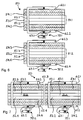
- the basic structure of an exemplified pixel 50 of a device according to the invention is illustrated in Figure 1 .
- the pixel 50 comprises, e.g., two light-sensitive photo sites 51.1, 51.2.
- a first photo site 51.1 has a first photo gate 52.1 for the phase angle 0° and a second photo gate 52.2 for the phase angle 180°;
- a second photo site 51.2 has a third photo gate 52.3 for the phase angle 90° and a fourth photo gate 52.4 for the phase angle 270°.
- the pixel 50 further comprises light-protected storage gates 54.1-54.4, each of which is associated to a photo gate 52.1-52.4.
- a first storage gate 54.1 is for storing signals with phase angle 0°
- a second storage gate 54.2 for storing signals with phase angle 180°
- a third storage gate 54.3 for storing signals with phase angle 90°
- a fourth storage gate 54.4 for storing signals with phase angle 270°.
- the second storage gate 54.2 and the third storage gate 54.3 are isolated by a separation gate 55. All gates within one pixel 50 can be controlled separately.
- the device according to the invention preferably comprises a standard objective 2 for imaging a scene 1, thus generating an imaged scene 3.
- the device further comprises a microlens array 4 and an optical application-specific integrated circuit (ASIC) 5.
- ASIC optical application-specific integrated circuit
- Each pixel 40 of the microlens array comprises an optical microstructure 41 which can be realized, e.g., as a microlens or a plurality of microlenses, as a diffractive element or a plurality of diffractive elements etc.
- the optical microstructure 41 aims at equally distributing the averaged light intensity of an imaged-scene pixel 30 onto the two optically identical photo sites 51.1, 51.2 of the ASIC pixel 50. This is schematically illustrated in Fig.
- the optical microstructure 41 consists of two sub-structures 42.1, 42.2.
- a first sub-structure 42.1 is for averaging the intensity
- a second sub-structure 42.2 is for distributing the averaged intensity onto the two photo sites 51.1, 51.2.
- the device according to the invention can preferably be realized in two different technologies:
- FIG. 4 An embodiment realized in a pure CCD process is shown in Figure 4 .
- One pixel 50.1 (50.2,...) consists of two light sensitive areas 51.1, 51.2. Each of these areas 51.1 (or 51.2, respectively) is divided into two or three light sensitive modulation gates 52.1, 52.2 (or 52.3, 52.4); here a 3-gate realization is shown with a middle photo gate 53.1 (or 53.2).
- the middle gate 53.1 (or 53.2) - if present - is kept at a fixed potential and the outer modulation gates 52.1, 52.2 (or 52.3, 52.4) are modulated in a balanced manner.
- Optically generated charge carriers are then distributed to the neighboring storage gates 54.1, 54.2 (or 54.3, 54.4), depending on the actual potential gradient under the modulation gates 52.1, 52.2 (or 52.3, 52.4).
- the storage gates 54.1, 54.2 (or 54.3, 54.4) are isolated from each other by an additional transportation gate 55.
- the two modulation-gate pairs 52.1, 52.2 and 52.3, 52.4 within one pixel 50.1 are operated with a 90° phase difference with respect to each other, so that the one pair 52.1, 52.2 integrates the in-phase component and the other pair 52.3, 52.4 integrates the quadrature-phase component.
- Each gate within the pixel 50.1 can be controlled individually and all pixels 50.1, 50.2,... are operated in parallel.
- the sensor is realized as a frame transfer CCD.
- a first, partly light-sensitive area 56 accessible to light serves as a lock-in CCD array for integration, and a second, light-protected area 57 serves as a memory CCD array for storage.
- the pixel gates are therefore operated like a 3-phase CCD to transfer the image into the storage CCD 57. It can then be read out protected from further optical signal distortion. During readout, the next image can be integrated.
- smearing may take place. This, however, does not seriously influence the measured phase result, since all sampling points belonging to one pixel 50.1 (50.2, ...) integrate the same parasitic offset charge.
- anti-blooming structures can be integrated in order to prevent charge carriers of an overexposed pixel to disturb neighboring pixel information. Additionally, a charge-dump diffusion 58 on top of the first area 56 enables to get rid of parasitic charge.
- the dimensions of the CCD gates are preferentially chosen such that one gets square pixels 50.1, 50.2,... (i.e., the gates are about 12 times wider than long).
- the proposed structure is an advantageous combination of the established frame-transfer-CCD principle with the new demodulation-pixel principle.
- the pixel can also be realized in CMOS/CCD technology with the active-pixel concept.
- the CMOS-APS/CCD realization seems to be more advantageous than a pure CCD realization, since each pixel can be addressed and read out individually, and blooming problems or smearing problems do not appear.
- Three different embodiments realized in the CMOS-APS/CCD technology are shown in Figures 5-7 .
- Figure 5 shows an embodiment which has only one readout stage per pixel 50.
- the single sampling points can then be transferred to a readout node sequentially by operating the CCD gates like a conventional CCD line. Care has to be taken that no additional charge is optically generated during this transfer.
- the pixel 50 comprises a dump gate 59 and a dump diffusion 60 for resetting, and an OUT gate 61 and a sense diffusion 62 for reading out.
- the pixel 50 additionally comprises an addressable in-pixel APS readout circuitry 70.
- Figure 6 and Figure 7 show embodiments with two readout stages 70.1, 70.2 per pixel 50.
- two sense diffusions 62.1, 62.2 (or 62.3, 62.4, respectively) are shortcircuited to one sense node 63.1 (or 63.2), which can be accessed from two sides.
- This enables the readout of two sampling points per readout stage without moving the sampled values through the light-sensitive CCD gates.
- the sense diffusion 62.1-62.4 will get a larger capacitance (less than a factor two) and hence a worse conversion factor (voltage increase per electron); however, this drawback can be tolerated.
- fixed-pattern noise due to the use of two readout stages 70.1, 70.2 per pixel 50 is not a problem.
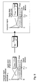
- FIGS 8 and 9 illustrate the operation principle of a TOF distance measurement system according to the state of the art.
- a modulated light source (or transmitter) 101 is normally located near a detector (or receiver) 103. Since the optical power density on an illuminated object or target 102 decreases with the square of the distance L between the illumination source 101 and the target 102, the received intensity I rec on the detector 103 also decreases with the square of the target distance L.
- a switch 105 in the receiver 103 opens. The switch 105 closes with the end of the light pulse 104.
- the amount of light integrated in the receiver 103 depends on the overlap of the time window 107 defined by the ON time of the switch 105 and the delayed time window 106 of ON time of the received light pulse 104.
- Both ON time of the switch 105 and pulse width are chosen to have the same length T.
- Targets 102 farther away from the light source 101 only integrate a fraction of the light pulse 104.
- Only distances L ⁇ L max within the propagation range of the light pulse 104, defined by half the product of the pulse width T and the light velocity c can be measured.
- the amount of received light I rec decreases with the square of the target distance L to the emitting active illumination source 101, as illustrated in Fig. 9.
- the prior-art shutter operation leads to an additional distance-dependent attenuation of the integrated received signal.
- a first mode of operation according to one aspect of the invention is illustrated in Figures 10 and 11 .
- the switch 105 is started at the end of the light-pulse transmission or even later.
- Targets 102 farther away from the range camera integrate a longer period of the light pulse 104 than targets 102 near the range camera.
- the resulting integrated signal share of the light pulse now only decreases linearly with the distance L of the target 102 (cf. Fig. 11).
- Figures 12 and 13 show a second mode of operation according to one aspect of the invention.
- This method uses a falling-ramp pulse 104 instead of a square pulse and combines this operation with the "inverse shutter operation" explained with respect to Figs. 10 and 11. This results in an integrated signal which does not depend on the target's distance L , only on its remission coefficient, if the target 102 is a Lambert reflector.
Abstract
Description
- Sinusoidal radiation signals are demodulated by operating the two photo sites and their storage areas in quadrature, i.e., by applying the clocking signals to the second photo site and its storage areas with a delay of a quarter of the repetition period compared to the first photo site and its storage areas.
- Pulsed radiation signals are measured by switching the first photo site's storage part from the first to the second area during the arrival of the radiation pulse. The second photo site and its storage areas are used for offset measurements without emitted and received radiation.
Prior to step (c), the electromagnetic radiation incident on a pixel is spatially averaged and the averaged electromagnetic radiation is equally distributed onto said transducer elements of the pixel.
- Each pixel can be addressed and read out individually. Thus regions of interest (ROI) can be defined, for example special regions can get a different illumination time or readout at a different frame rate.
- No blooming problems like with CCDs will appear. Charge of an overexposed pixel is dumped to a dump node or to the sense node and does not disturb neighboring pixels.
- No smearing problems like with CCD will appear. Instead of moving the pixel charge through the entire imager, the charge is converted to a voltage within each pixel.

- The information is only gained when referencing these results to the "dark measurement" (no illumination) and to the "light measurement" (non-modulated DC illumination with the active illumination source). The result of the latter measurement depends on the distance of the object. Illuminated objects farther away from the camera are darker than those near the camera. Only with these reference measurements the distance can be calculated. The advantage is that we get a constant signal-to-noise ratio for the modulated measurement over the complete range. And, since the signal does not depend on the distance for this measurement, a special high dynamic range of the sensor is not necessary.
- It is of course not true for a realistic scene that all surfaces exactly behave like Lambert reflectors, meaning that the light intensity decreases with the square of the object distance. So the measurement still contains information.
- The three or four phase measurements (or temporal sampling points) used for demodulation of the phase information of the received signal can be performed simultaneously, i.e. in parallel, rather than sequentially.
- The overall pixel size is small. This invention is therefore ideally suited for realization as a large array (several 10'000 pixels to several 100'000 pixels).
- The invention offers a large fill factor of > 50 % (without microlenses) and of up to 100 % if microlenses are used.
- Two optically identical photo sites are used for in-phase and quadrature-phase signal acquisition. Therefore, the pixels are not sensitive on local scene differences within the scene detail imaged to one pixel.
- Due to the simple, highly symmetrical architecture of the pixel, a very efficient realization of a microlens structure is possible, leading to up to an effective fill factor of 100 %. In addition, the assembly and positioning of the microlens array becomes relatively easy because of its extension in only 1 dimension.
- The invention is robust against device noise, since no active electronics is used at a point of time where the signal is low. Instead, the post-processing is performed only when the integrated signal is strong enough.
- The various sampling points are offset free (or at least pair-wise offset free, depending on the realization in pure CCD or CMOS-APS/CCD technology).
- A TOF system can be operated with a resolution independent of the object distance.
- Figure 1
- shows a basic concept of a pixel of a device according to the invention.
- Figure 2
- shows a device according to the invention.
- Figure 3
- shows a pixel of the device of Figure 2 together with an associated microlens.
- Figure 4
- shows an embodiment of the invention realized in CCD technology.
- Figures 5-7
- show three different embodiments of the invention realized in CMOS-APS/CCD technology.
- Figures 8 and 9
- show the principle of a pulsed-TOF distance-measurement method according to the state of the art.
- Figures 10 and 11
- show the principle of a first embodiment of a pulsed-TOF distance-measurement method according to the invention.
- Figures 12 and 13
- show the principle of a second embodiment of a pulsed-TOF distance-measurement method according to the invention.
Claims (18)
- A device for spatially resolved photodetection and demodulation of temporally modulated elctromagnetic waves, comprisinga one-dimensional or two-dimensional arrangement of pixels (50), a pixel (50) comprising
at least two elements (51.1, 51.2) for transducing incident electromagnetic radiation into an electric signal, each transducer element (51.1, 51.2) being associated with
at least one element (54.1-54.4) for storing said electric signal, said at least one storage element (54.1-54.4) being inaccessible or insensitive to incident electromagnetic radiation,
characterized in thata pixel (50) comprises an optical element (41) for spatially averaging the electromagnetic radiation incident on the pixel (50) and equally distributing the averaged electromagnetic radiation onto said transducer elements (51.1, 51.2) of the pixel (50). - The device according to claim 1, wherein said optical element (41) comprises a refractive and/or diffractive optical element.
- The device according to claim 1 or 2, wherein a pixel (50) has two transducer elements (51.1, 51.2).
- The device according to one of the claims 1-3, wherein each transducer element (51.1) is associated with two storage elements (54.1, 54.2).
- The device according to one of the claims 1-4, wherein said arrangement of pixels (50) is realized in CCD or in CMOS-APS/CCD technology.
- A method for spatially resolved photodetection and demodulation of temporally modulated elctromagnetic waves, comprising the steps ofcharacterized in that(a) impinging electromagnetic radiation onto a one-dimensional or two-dimensional arrangement of pixels (50),(b) transducing electromagnetic radiation incident on a pixel (50) into at least two electric signals in at least two transducer elements (51.1, 51.2), and(c) storing each of said at least two electric signals in at least one storage element (54.1-54.4),
prior to step (c), the electromagnetic radiation incident on a pixel (50) is spatially averaged and the averaged electromagnetic radiation is equally distributed onto said transducer elements (51.1, 51.2) of the pixel (50). - The method according to claim 6, wherein two transducer elements (51.1, 51.2) of a pixel (50) are operated with a 90° phase shift with respect to each other.
- The method according to claim 6 or 7, wherein each pixel (50) is addressed and read out individually.
- A device for determining a distance (L) between said device and an object (102), comprisingcharacterized bymeans (101) for emitting during a first limited time interval pulsed electromagnetic radiation (104), andmeans (103), preferably according to one of the claims 1-5, for detecting incident electromagnetic radiation during a second limited time interval (107),
means (105) for controlling said emitting (101) and detecting means (103) such that said first and said second time intervals do not overlap. - The device according to claim 9, whereby said controlling means (105) are such that said first and said second time intervals have essentially the same duration (T).
- The device according to claims 9 or 10, whereby said controlling means (105) are such that said second time interval begins at the moment when said first time interval ends.
- The device according to one of the claims 9-11, whereby said emitting means (101) are for emitting square pulses or falling ramp pulses.
- The device according to one of the claims 9-12, whereby the sensitivity of said detecting means (103) and/or the form of said pulses (104) are chosen such that their product is a linearly decreasing function of time.
- A method for determining a distance (L) between a measurement system and an object (102), comprising the steps ofcharacterized in thatemitting during a first limited time interval a pulse (104) of electromagnetic radiation from said measurement system towards said object (102),reflecting and/or scattering at least part of said electromagnetic radiation from said object, anddetecting, preferably according to one of the claims 6-8, during a second limited time interval (107) electromagnetic radiation reflected and/or scattered from said object (102),
said first and said second time intervals do not overlap. - The method according to claim 14, whereby said first and said second time intervals have essentially the same duration (T).
- The method according to claims 14 or 15, whereby said second time interval begins at the moment when said first time interval ends.
- The method according to one of the claims 14-16, whereby said pulse (104) is a square pulse or a falling ramp pulse.
- The method according to one of the claims 14-17, whereby a detecting sensitivity and/or the form of said pulse are chosen such that their product is a linearly decreasing function of time.
Priority Applications (4)
| Application Number | Priority Date | Filing Date | Title |
|---|---|---|---|
| EP00109271A EP1152261A1 (en) | 2000-04-28 | 2000-04-28 | Device and method for spatially resolved photodetection and demodulation of modulated electromagnetic waves |
| US10/258,784 US7060957B2 (en) | 2000-04-28 | 2001-03-26 | Device and method for spatially resolved photodetection and demodulation of modulated electromagnetic waves |
| PCT/CH2001/000184 WO2001084182A1 (en) | 2000-04-28 | 2001-03-26 | Device and method for spatially resolved photodetection and demodulation of modulated electromagnetic waves |
| JP2001581152A JP2003532122A (en) | 2000-04-28 | 2001-03-26 | Apparatus and method for spatially resolving a modulated electromagnetic wave to detect and demodulate light |
Applications Claiming Priority (1)
| Application Number | Priority Date | Filing Date | Title |
|---|---|---|---|
| EP00109271A EP1152261A1 (en) | 2000-04-28 | 2000-04-28 | Device and method for spatially resolved photodetection and demodulation of modulated electromagnetic waves |
Publications (1)
| Publication Number | Publication Date |
|---|---|
| EP1152261A1 true EP1152261A1 (en) | 2001-11-07 |
Family
ID=8168592
Family Applications (1)
| Application Number | Title | Priority Date | Filing Date |
|---|---|---|---|
| EP00109271A Withdrawn EP1152261A1 (en) | 2000-04-28 | 2000-04-28 | Device and method for spatially resolved photodetection and demodulation of modulated electromagnetic waves |
Country Status (4)
| Country | Link |
|---|---|
| US (1) | US7060957B2 (en) |
| EP (1) | EP1152261A1 (en) |
| JP (1) | JP2003532122A (en) |
| WO (1) | WO2001084182A1 (en) |
Cited By (24)
| Publication number | Priority date | Publication date | Assignee | Title |
|---|---|---|---|---|
| WO2003073602A2 (en) * | 2002-02-22 | 2003-09-04 | Rudolf Schwarte | Method and device for detecting and processing electric and optical signals |
| WO2004008175A1 (en) * | 2002-07-15 | 2004-01-22 | Matsushita Electric Works, Ltd. | Light receiving device with controllable sensitivity and spatial information detecting apparatus using the same |
| WO2005052633A1 (en) * | 2003-10-29 | 2005-06-09 | Fraunhofer-Gesellschaft zur Förderung der angewandten Forschung e.V. | Distance sensor and method for distance detection |
| EP1622200A1 (en) * | 2004-07-26 | 2006-02-01 | CSEM Centre Suisse d'Electronique et de Microtechnique SA | Solid-state photodetector pixel and photodetecting method |
| DE102004038302A1 (en) * | 2004-08-04 | 2006-03-16 | Iris-Gmbh Infrared & Intelligent Sensors | Medical diagnosis expert system has camera producing sequence of 3D images with processor determining treatment recommendation for spoken output |
| EP1752793A1 (en) | 2005-08-08 | 2007-02-14 | CSEM Centre Suisse d'Electronique et de Microtechnique SA | Method and device for redundant distance measurement and mismatch cancellation in phase-measurement systems |
| EP1762862A1 (en) | 2005-09-09 | 2007-03-14 | IEE INTERNATIONAL ELECTRONICS & ENGINEERING S.A. | Method and device for 3D imaging |
| EP1952752A1 (en) * | 2007-01-31 | 2008-08-06 | Richard Wolf GmbH | Endoscope system |
| US7498621B2 (en) | 2002-06-20 | 2009-03-03 | Mesa Imaging Ag | Image sensing device and method of |
| US7560701B2 (en) | 2005-08-12 | 2009-07-14 | Mesa Imaging Ag | Highly sensitive, fast pixel for use in an image sensor |
| EP2264481A1 (en) | 2009-06-04 | 2010-12-22 | IEE International Electronics & Engineering S.A. | Method and device for acquiring a range image |
| WO2011000815A1 (en) | 2009-07-01 | 2011-01-06 | Iee International Electronics & Engineering S.A. | Range camera and range image acquisition method |
| WO2011020921A1 (en) | 2009-08-21 | 2011-02-24 | Iee International Electronics & Engineering S.A. | Time-of-flight sensor |
| EP2302564A1 (en) | 2009-09-23 | 2011-03-30 | Iee International Electronics & Engineering S.A. | Real-time dynamic reference image generation for range imaging system |
| US7923673B2 (en) | 2004-08-04 | 2011-04-12 | Mesa Imaging Ag | Large-area pixel for use in an image sensor |
| WO2011117162A1 (en) | 2010-03-25 | 2011-09-29 | Iee International Electronics & Engineering S.A. | Optoelectronic sensor and method for detecting impinging-light attribute |
| DE102005011116B4 (en) * | 2005-03-10 | 2012-03-15 | Agtatec Ag | Device for controlling and / or monitoring a grand piano |
| US8210175B2 (en) | 2007-02-09 | 2012-07-03 | B/E Aerospace Systems Gmbh | Method and apparatus for emergency supply of oxygen in an aircraft |
| WO2014000793A1 (en) | 2012-06-27 | 2014-01-03 | Teledyne Dalsa B.V. | Image sensor and apparatus comprising such image sensor |
| WO2017050633A1 (en) * | 2015-09-21 | 2017-03-30 | Photonic Vision Limited | Time of flight distance sensor |
| CN107430192A (en) * | 2015-03-31 | 2017-12-01 | 谷歌公司 | Increase the method and apparatus of the frame rate of flight time measurement |
| WO2019162298A1 (en) * | 2018-02-20 | 2019-08-29 | Iris-Gmbh Infrared & Intelligent Sensors | Device and method for door area monitoring |
| US10401496B2 (en) | 2015-09-30 | 2019-09-03 | Ams Sensors Singapore Pte. Ltd. | Optoelectronic modules operable to collect distance data via time-of-flight and triangulation |
| CN114175618A (en) * | 2019-08-01 | 2022-03-11 | 布鲁克曼科技株式会社 | Distance image capturing apparatus and distance image capturing method |
Families Citing this family (279)
| Publication number | Priority date | Publication date | Assignee | Title |
|---|---|---|---|---|
| US8352400B2 (en) | 1991-12-23 | 2013-01-08 | Hoffberg Steven M | Adaptive pattern recognition based controller apparatus and method and human-factored interface therefore |
| US7966078B2 (en) | 1999-02-01 | 2011-06-21 | Steven Hoffberg | Network media appliance system and method |
| US6990639B2 (en) | 2002-02-07 | 2006-01-24 | Microsoft Corporation | System and process for controlling electronic components in a ubiquitous computing environment using multimodal integration |
| US7665041B2 (en) | 2003-03-25 | 2010-02-16 | Microsoft Corporation | Architecture for controlling a computer using hand gestures |
| US8745541B2 (en) | 2003-03-25 | 2014-06-03 | Microsoft Corporation | Architecture for controlling a computer using hand gestures |
| US7545494B2 (en) * | 2003-07-23 | 2009-06-09 | Bayer Technology Services Gmbh | Analytical system and method for analyzing nonlinear optical signals |
| JP4660086B2 (en) * | 2003-12-01 | 2011-03-30 | 三洋電機株式会社 | Solid-state image sensor |
| JP4280822B2 (en) * | 2004-02-18 | 2009-06-17 | 国立大学法人静岡大学 | Optical time-of-flight distance sensor |
| WO2006030989A1 (en) | 2004-09-17 | 2006-03-23 | Matsushita Electric Works, Ltd. | A range image sensor |
| JP2006337286A (en) * | 2005-06-03 | 2006-12-14 | Ricoh Co Ltd | Shape-measuring device |
| CN101213429B (en) * | 2005-06-27 | 2012-02-08 | Hl-平面技术有限公司 | Device for detecting electromagnetic wave and method for producing the same |
| EP1746410B1 (en) * | 2005-07-21 | 2018-08-22 | CSEM Centre Suisse d'Electronique et de Microtechnique SA - Recherche et Développement | Apparatus and method for fluorescence lifetime imaging |
| US7697827B2 (en) | 2005-10-17 | 2010-04-13 | Konicek Jeffrey C | User-friendlier interfaces for a camera |
| US8355117B2 (en) | 2005-12-21 | 2013-01-15 | Ecole Polytechnique Federale De Lausanne | Method and arrangement for measuring the distance to an object |
| WO2008047640A1 (en) * | 2006-10-18 | 2008-04-24 | Panasonic Electric Works Co., Ltd. | Spatial information detecting device |
| DE602006007361D1 (en) * | 2006-10-24 | 2009-07-30 | Fiat Ricerche | Optical method and apparatus for measuring the distance from an obstacle |
| US8005238B2 (en) | 2007-03-22 | 2011-08-23 | Microsoft Corporation | Robust adaptive beamforming with enhanced noise suppression |
| US8005237B2 (en) | 2007-05-17 | 2011-08-23 | Microsoft Corp. | Sensor array beamformer post-processor |
| US8629976B2 (en) | 2007-10-02 | 2014-01-14 | Microsoft Corporation | Methods and systems for hierarchical de-aliasing time-of-flight (TOF) systems |
| US8385557B2 (en) | 2008-06-19 | 2013-02-26 | Microsoft Corporation | Multichannel acoustic echo reduction |
| US8325909B2 (en) | 2008-06-25 | 2012-12-04 | Microsoft Corporation | Acoustic echo suppression |
| US8203699B2 (en) | 2008-06-30 | 2012-06-19 | Microsoft Corporation | System architecture design for time-of-flight system having reduced differential pixel size, and time-of-flight systems so designed |
| US8681321B2 (en) | 2009-01-04 | 2014-03-25 | Microsoft International Holdings B.V. | Gated 3D camera |
| US8294767B2 (en) | 2009-01-30 | 2012-10-23 | Microsoft Corporation | Body scan |
| US8565476B2 (en) | 2009-01-30 | 2013-10-22 | Microsoft Corporation | Visual target tracking |
| US20100199231A1 (en) | 2009-01-30 | 2010-08-05 | Microsoft Corporation | Predictive determination |
| US8588465B2 (en) | 2009-01-30 | 2013-11-19 | Microsoft Corporation | Visual target tracking |
| US8682028B2 (en) | 2009-01-30 | 2014-03-25 | Microsoft Corporation | Visual target tracking |
| US8448094B2 (en) * | 2009-01-30 | 2013-05-21 | Microsoft Corporation | Mapping a natural input device to a legacy system |
| US8295546B2 (en) | 2009-01-30 | 2012-10-23 | Microsoft Corporation | Pose tracking pipeline |
| US8267781B2 (en) | 2009-01-30 | 2012-09-18 | Microsoft Corporation | Visual target tracking |
| US8577085B2 (en) | 2009-01-30 | 2013-11-05 | Microsoft Corporation | Visual target tracking |
| US8565477B2 (en) | 2009-01-30 | 2013-10-22 | Microsoft Corporation | Visual target tracking |
| US8487938B2 (en) | 2009-01-30 | 2013-07-16 | Microsoft Corporation | Standard Gestures |
| US7996793B2 (en) | 2009-01-30 | 2011-08-09 | Microsoft Corporation | Gesture recognizer system architecture |
| US8577084B2 (en) | 2009-01-30 | 2013-11-05 | Microsoft Corporation | Visual target tracking |
| US8773355B2 (en) | 2009-03-16 | 2014-07-08 | Microsoft Corporation | Adaptive cursor sizing |
| US8988437B2 (en) | 2009-03-20 | 2015-03-24 | Microsoft Technology Licensing, Llc | Chaining animations |
| US9256282B2 (en) | 2009-03-20 | 2016-02-09 | Microsoft Technology Licensing, Llc | Virtual object manipulation |
| US9313376B1 (en) | 2009-04-01 | 2016-04-12 | Microsoft Technology Licensing, Llc | Dynamic depth power equalization |
| US8181123B2 (en) | 2009-05-01 | 2012-05-15 | Microsoft Corporation | Managing virtual port associations to users in a gesture-based computing environment |
| US8942428B2 (en) | 2009-05-01 | 2015-01-27 | Microsoft Corporation | Isolate extraneous motions |
| US9898675B2 (en) | 2009-05-01 | 2018-02-20 | Microsoft Technology Licensing, Llc | User movement tracking feedback to improve tracking |
| US9377857B2 (en) | 2009-05-01 | 2016-06-28 | Microsoft Technology Licensing, Llc | Show body position |
| US9015638B2 (en) | 2009-05-01 | 2015-04-21 | Microsoft Technology Licensing, Llc | Binding users to a gesture based system and providing feedback to the users |
| US8503720B2 (en) | 2009-05-01 | 2013-08-06 | Microsoft Corporation | Human body pose estimation |
| US8253746B2 (en) | 2009-05-01 | 2012-08-28 | Microsoft Corporation | Determine intended motions |
| US8638985B2 (en) * | 2009-05-01 | 2014-01-28 | Microsoft Corporation | Human body pose estimation |
| US8340432B2 (en) | 2009-05-01 | 2012-12-25 | Microsoft Corporation | Systems and methods for detecting a tilt angle from a depth image |
| US9498718B2 (en) | 2009-05-01 | 2016-11-22 | Microsoft Technology Licensing, Llc | Altering a view perspective within a display environment |
| US8649554B2 (en) | 2009-05-01 | 2014-02-11 | Microsoft Corporation | Method to control perspective for a camera-controlled computer |
| US8660303B2 (en) | 2009-05-01 | 2014-02-25 | Microsoft Corporation | Detection of body and props |
| US8509479B2 (en) | 2009-05-29 | 2013-08-13 | Microsoft Corporation | Virtual object |
| US9400559B2 (en) | 2009-05-29 | 2016-07-26 | Microsoft Technology Licensing, Llc | Gesture shortcuts |
| US8744121B2 (en) | 2009-05-29 | 2014-06-03 | Microsoft Corporation | Device for identifying and tracking multiple humans over time |
| US8320619B2 (en) | 2009-05-29 | 2012-11-27 | Microsoft Corporation | Systems and methods for tracking a model |
| US8693724B2 (en) | 2009-05-29 | 2014-04-08 | Microsoft Corporation | Method and system implementing user-centric gesture control |
| US8542252B2 (en) | 2009-05-29 | 2013-09-24 | Microsoft Corporation | Target digitization, extraction, and tracking |
| US9182814B2 (en) | 2009-05-29 | 2015-11-10 | Microsoft Technology Licensing, Llc | Systems and methods for estimating a non-visible or occluded body part |
| US9383823B2 (en) | 2009-05-29 | 2016-07-05 | Microsoft Technology Licensing, Llc | Combining gestures beyond skeletal |
| US8418085B2 (en) | 2009-05-29 | 2013-04-09 | Microsoft Corporation | Gesture coach |
| US8856691B2 (en) | 2009-05-29 | 2014-10-07 | Microsoft Corporation | Gesture tool |
| US8379101B2 (en) | 2009-05-29 | 2013-02-19 | Microsoft Corporation | Environment and/or target segmentation |
| US8625837B2 (en) | 2009-05-29 | 2014-01-07 | Microsoft Corporation | Protocol and format for communicating an image from a camera to a computing environment |
| US8487871B2 (en) | 2009-06-01 | 2013-07-16 | Microsoft Corporation | Virtual desktop coordinate transformation |
| US8390680B2 (en) | 2009-07-09 | 2013-03-05 | Microsoft Corporation | Visual representation expression based on player expression |
| US9159151B2 (en) | 2009-07-13 | 2015-10-13 | Microsoft Technology Licensing, Llc | Bringing a visual representation to life via learned input from the user |
| DE102009037596B4 (en) | 2009-08-14 | 2014-07-24 | Fraunhofer-Gesellschaft zur Förderung der angewandten Forschung e.V. | Pixel structure, system and method for optical distance measurement and control circuit for the pixel structure |
| US8264536B2 (en) | 2009-08-25 | 2012-09-11 | Microsoft Corporation | Depth-sensitive imaging via polarization-state mapping |
| US9141193B2 (en) | 2009-08-31 | 2015-09-22 | Microsoft Technology Licensing, Llc | Techniques for using human gestures to control gesture unaware programs |
| US8508919B2 (en) | 2009-09-14 | 2013-08-13 | Microsoft Corporation | Separation of electrical and optical components |
| US8330134B2 (en) | 2009-09-14 | 2012-12-11 | Microsoft Corporation | Optical fault monitoring |
| US8976986B2 (en) | 2009-09-21 | 2015-03-10 | Microsoft Technology Licensing, Llc | Volume adjustment based on listener position |
| US8428340B2 (en) | 2009-09-21 | 2013-04-23 | Microsoft Corporation | Screen space plane identification |
| US8760571B2 (en) | 2009-09-21 | 2014-06-24 | Microsoft Corporation | Alignment of lens and image sensor |
| US9014546B2 (en) | 2009-09-23 | 2015-04-21 | Rovi Guides, Inc. | Systems and methods for automatically detecting users within detection regions of media devices |
| US8452087B2 (en) | 2009-09-30 | 2013-05-28 | Microsoft Corporation | Image selection techniques |
| US8723118B2 (en) | 2009-10-01 | 2014-05-13 | Microsoft Corporation | Imager for constructing color and depth images |
| US8564534B2 (en) | 2009-10-07 | 2013-10-22 | Microsoft Corporation | Human tracking system |
| US8867820B2 (en) | 2009-10-07 | 2014-10-21 | Microsoft Corporation | Systems and methods for removing a background of an image |
| US7961910B2 (en) | 2009-10-07 | 2011-06-14 | Microsoft Corporation | Systems and methods for tracking a model |
| US8963829B2 (en) | 2009-10-07 | 2015-02-24 | Microsoft Corporation | Methods and systems for determining and tracking extremities of a target |
| US9400548B2 (en) | 2009-10-19 | 2016-07-26 | Microsoft Technology Licensing, Llc | Gesture personalization and profile roaming |
| US8988432B2 (en) | 2009-11-05 | 2015-03-24 | Microsoft Technology Licensing, Llc | Systems and methods for processing an image for target tracking |
| US8843857B2 (en) | 2009-11-19 | 2014-09-23 | Microsoft Corporation | Distance scalable no touch computing |
| US9244533B2 (en) | 2009-12-17 | 2016-01-26 | Microsoft Technology Licensing, Llc | Camera navigation for presentations |
| US20110150271A1 (en) | 2009-12-18 | 2011-06-23 | Microsoft Corporation | Motion detection using depth images |
| US8320621B2 (en) | 2009-12-21 | 2012-11-27 | Microsoft Corporation | Depth projector system with integrated VCSEL array |
| US9268404B2 (en) | 2010-01-08 | 2016-02-23 | Microsoft Technology Licensing, Llc | Application gesture interpretation |
| US9019201B2 (en) | 2010-01-08 | 2015-04-28 | Microsoft Technology Licensing, Llc | Evolving universal gesture sets |
| US8631355B2 (en) | 2010-01-08 | 2014-01-14 | Microsoft Corporation | Assigning gesture dictionaries |
| US8334842B2 (en) | 2010-01-15 | 2012-12-18 | Microsoft Corporation | Recognizing user intent in motion capture system |
| US8933884B2 (en) | 2010-01-15 | 2015-01-13 | Microsoft Corporation | Tracking groups of users in motion capture system |
| US8676581B2 (en) | 2010-01-22 | 2014-03-18 | Microsoft Corporation | Speech recognition analysis via identification information |
| US8265341B2 (en) | 2010-01-25 | 2012-09-11 | Microsoft Corporation | Voice-body identity correlation |
| US8864581B2 (en) | 2010-01-29 | 2014-10-21 | Microsoft Corporation | Visual based identitiy tracking |
| US8891067B2 (en) | 2010-02-01 | 2014-11-18 | Microsoft Corporation | Multiple synchronized optical sources for time-of-flight range finding systems |
| US8619122B2 (en) | 2010-02-02 | 2013-12-31 | Microsoft Corporation | Depth camera compatibility |
| US8687044B2 (en) | 2010-02-02 | 2014-04-01 | Microsoft Corporation | Depth camera compatibility |
| US8717469B2 (en) | 2010-02-03 | 2014-05-06 | Microsoft Corporation | Fast gating photosurface |
| KR101681198B1 (en) * | 2010-02-04 | 2016-12-01 | 삼성전자주식회사 | Sensor, method of operating the sensor, and system having the sensor |
| US8499257B2 (en) | 2010-02-09 | 2013-07-30 | Microsoft Corporation | Handles interactions for human—computer interface |
| US8659658B2 (en) | 2010-02-09 | 2014-02-25 | Microsoft Corporation | Physical interaction zone for gesture-based user interfaces |
| US20110199302A1 (en) * | 2010-02-16 | 2011-08-18 | Microsoft Corporation | Capturing screen objects using a collision volume |
| US8633890B2 (en) | 2010-02-16 | 2014-01-21 | Microsoft Corporation | Gesture detection based on joint skipping |
| US8928579B2 (en) | 2010-02-22 | 2015-01-06 | Andrew David Wilson | Interacting with an omni-directionally projected display |
| US8422769B2 (en) | 2010-03-05 | 2013-04-16 | Microsoft Corporation | Image segmentation using reduced foreground training data |
| US8655069B2 (en) | 2010-03-05 | 2014-02-18 | Microsoft Corporation | Updating image segmentation following user input |
| US8411948B2 (en) | 2010-03-05 | 2013-04-02 | Microsoft Corporation | Up-sampling binary images for segmentation |
| US20110223995A1 (en) | 2010-03-12 | 2011-09-15 | Kevin Geisner | Interacting with a computer based application |
| US8279418B2 (en) | 2010-03-17 | 2012-10-02 | Microsoft Corporation | Raster scanning for depth detection |
| US8213680B2 (en) | 2010-03-19 | 2012-07-03 | Microsoft Corporation | Proxy training data for human body tracking |
| US8514269B2 (en) | 2010-03-26 | 2013-08-20 | Microsoft Corporation | De-aliasing depth images |
| US8523667B2 (en) | 2010-03-29 | 2013-09-03 | Microsoft Corporation | Parental control settings based on body dimensions |
| US8605763B2 (en) | 2010-03-31 | 2013-12-10 | Microsoft Corporation | Temperature measurement and control for laser and light-emitting diodes |
| US9646340B2 (en) | 2010-04-01 | 2017-05-09 | Microsoft Technology Licensing, Llc | Avatar-based virtual dressing room |
| US9098873B2 (en) | 2010-04-01 | 2015-08-04 | Microsoft Technology Licensing, Llc | Motion-based interactive shopping environment |
| US8351651B2 (en) | 2010-04-26 | 2013-01-08 | Microsoft Corporation | Hand-location post-process refinement in a tracking system |
| US8379919B2 (en) | 2010-04-29 | 2013-02-19 | Microsoft Corporation | Multiple centroid condensation of probability distribution clouds |
| US8284847B2 (en) | 2010-05-03 | 2012-10-09 | Microsoft Corporation | Detecting motion for a multifunction sensor device |
| US8885890B2 (en) | 2010-05-07 | 2014-11-11 | Microsoft Corporation | Depth map confidence filtering |
| US8498481B2 (en) | 2010-05-07 | 2013-07-30 | Microsoft Corporation | Image segmentation using star-convexity constraints |
| US8457353B2 (en) | 2010-05-18 | 2013-06-04 | Microsoft Corporation | Gestures and gesture modifiers for manipulating a user-interface |
| US8803888B2 (en) | 2010-06-02 | 2014-08-12 | Microsoft Corporation | Recognition system for sharing information |
| US8751215B2 (en) | 2010-06-04 | 2014-06-10 | Microsoft Corporation | Machine based sign language interpreter |
| US9008355B2 (en) | 2010-06-04 | 2015-04-14 | Microsoft Technology Licensing, Llc | Automatic depth camera aiming |
| US9557574B2 (en) | 2010-06-08 | 2017-01-31 | Microsoft Technology Licensing, Llc | Depth illumination and detection optics |
| US8330822B2 (en) | 2010-06-09 | 2012-12-11 | Microsoft Corporation | Thermally-tuned depth camera light source |
| US8675981B2 (en) | 2010-06-11 | 2014-03-18 | Microsoft Corporation | Multi-modal gender recognition including depth data |
| US9384329B2 (en) | 2010-06-11 | 2016-07-05 | Microsoft Technology Licensing, Llc | Caloric burn determination from body movement |
| US8749557B2 (en) | 2010-06-11 | 2014-06-10 | Microsoft Corporation | Interacting with user interface via avatar |
| US8982151B2 (en) | 2010-06-14 | 2015-03-17 | Microsoft Technology Licensing, Llc | Independently processing planes of display data |
| US8670029B2 (en) | 2010-06-16 | 2014-03-11 | Microsoft Corporation | Depth camera illuminator with superluminescent light-emitting diode |
| US8558873B2 (en) | 2010-06-16 | 2013-10-15 | Microsoft Corporation | Use of wavefront coding to create a depth image |
| US8296151B2 (en) | 2010-06-18 | 2012-10-23 | Microsoft Corporation | Compound gesture-speech commands |
| US8381108B2 (en) | 2010-06-21 | 2013-02-19 | Microsoft Corporation | Natural user input for driving interactive stories |
| US8416187B2 (en) | 2010-06-22 | 2013-04-09 | Microsoft Corporation | Item navigation using motion-capture data |
| US9075434B2 (en) | 2010-08-20 | 2015-07-07 | Microsoft Technology Licensing, Llc | Translating user motion into multiple object responses |
| US8613666B2 (en) | 2010-08-31 | 2013-12-24 | Microsoft Corporation | User selection and navigation based on looped motions |
| US20120058824A1 (en) | 2010-09-07 | 2012-03-08 | Microsoft Corporation | Scalable real-time motion recognition |
| US8437506B2 (en) | 2010-09-07 | 2013-05-07 | Microsoft Corporation | System for fast, probabilistic skeletal tracking |
| US8988508B2 (en) | 2010-09-24 | 2015-03-24 | Microsoft Technology Licensing, Llc. | Wide angle field of view active illumination imaging system |
| US8681255B2 (en) | 2010-09-28 | 2014-03-25 | Microsoft Corporation | Integrated low power depth camera and projection device |
| US8548270B2 (en) | 2010-10-04 | 2013-10-01 | Microsoft Corporation | Time-of-flight depth imaging |
| US9484065B2 (en) | 2010-10-15 | 2016-11-01 | Microsoft Technology Licensing, Llc | Intelligent determination of replays based on event identification |
| US8592739B2 (en) | 2010-11-02 | 2013-11-26 | Microsoft Corporation | Detection of configuration changes of an optical element in an illumination system |
| US8866889B2 (en) | 2010-11-03 | 2014-10-21 | Microsoft Corporation | In-home depth camera calibration |
| US8667519B2 (en) | 2010-11-12 | 2014-03-04 | Microsoft Corporation | Automatic passive and anonymous feedback system |
| US10726861B2 (en) | 2010-11-15 | 2020-07-28 | Microsoft Technology Licensing, Llc | Semi-private communication in open environments |
| US9349040B2 (en) | 2010-11-19 | 2016-05-24 | Microsoft Technology Licensing, Llc | Bi-modal depth-image analysis |
| KR101812035B1 (en) * | 2010-11-30 | 2017-12-26 | 삼성전자 주식회사 | Image sensor and method for obtaining color image and depth image simultaneously |
| US10234545B2 (en) | 2010-12-01 | 2019-03-19 | Microsoft Technology Licensing, Llc | Light source module |
| US8553934B2 (en) | 2010-12-08 | 2013-10-08 | Microsoft Corporation | Orienting the position of a sensor |
| US8618405B2 (en) | 2010-12-09 | 2013-12-31 | Microsoft Corp. | Free-space gesture musical instrument digital interface (MIDI) controller |
| US8408706B2 (en) | 2010-12-13 | 2013-04-02 | Microsoft Corporation | 3D gaze tracker |
| KR101798063B1 (en) | 2010-12-14 | 2017-11-15 | 삼성전자주식회사 | Illumination optical system and 3D image acquisition apparatus including the same |
| KR101691156B1 (en) | 2010-12-14 | 2016-12-30 | 삼성전자주식회사 | Optical system having integrated illumination and imaging systems and 3D image acquisition apparatus including the optical system |
| US8920241B2 (en) | 2010-12-15 | 2014-12-30 | Microsoft Corporation | Gesture controlled persistent handles for interface guides |
| US9171264B2 (en) | 2010-12-15 | 2015-10-27 | Microsoft Technology Licensing, Llc | Parallel processing machine learning decision tree training |
| US8884968B2 (en) | 2010-12-15 | 2014-11-11 | Microsoft Corporation | Modeling an object from image data |
| US8448056B2 (en) | 2010-12-17 | 2013-05-21 | Microsoft Corporation | Validation analysis of human target |
| US8803952B2 (en) | 2010-12-20 | 2014-08-12 | Microsoft Corporation | Plural detector time-of-flight depth mapping |
| US9848106B2 (en) | 2010-12-21 | 2017-12-19 | Microsoft Technology Licensing, Llc | Intelligent gameplay photo capture |
| US8994718B2 (en) | 2010-12-21 | 2015-03-31 | Microsoft Technology Licensing, Llc | Skeletal control of three-dimensional virtual world |
| US9821224B2 (en) | 2010-12-21 | 2017-11-21 | Microsoft Technology Licensing, Llc | Driving simulator control with virtual skeleton |
| US9823339B2 (en) | 2010-12-21 | 2017-11-21 | Microsoft Technology Licensing, Llc | Plural anode time-of-flight sensor |
| US8385596B2 (en) | 2010-12-21 | 2013-02-26 | Microsoft Corporation | First person shooter control with virtual skeleton |
| US9123316B2 (en) | 2010-12-27 | 2015-09-01 | Microsoft Technology Licensing, Llc | Interactive content creation |
| US8488888B2 (en) | 2010-12-28 | 2013-07-16 | Microsoft Corporation | Classification of posture states |
| EP2477043A1 (en) * | 2011-01-12 | 2012-07-18 | Sony Corporation | 3D time-of-flight camera and method |
| US9247238B2 (en) | 2011-01-31 | 2016-01-26 | Microsoft Technology Licensing, Llc | Reducing interference between multiple infra-red depth cameras |
| US8401225B2 (en) | 2011-01-31 | 2013-03-19 | Microsoft Corporation | Moving object segmentation using depth images |
| US8587583B2 (en) | 2011-01-31 | 2013-11-19 | Microsoft Corporation | Three-dimensional environment reconstruction |
| US8401242B2 (en) | 2011-01-31 | 2013-03-19 | Microsoft Corporation | Real-time camera tracking using depth maps |
| US8724887B2 (en) | 2011-02-03 | 2014-05-13 | Microsoft Corporation | Environmental modifications to mitigate environmental factors |
| US8942917B2 (en) | 2011-02-14 | 2015-01-27 | Microsoft Corporation | Change invariant scene recognition by an agent |
| US8497838B2 (en) | 2011-02-16 | 2013-07-30 | Microsoft Corporation | Push actuation of interface controls |
| US9551914B2 (en) | 2011-03-07 | 2017-01-24 | Microsoft Technology Licensing, Llc | Illuminator with refractive optical element |
| US9067136B2 (en) | 2011-03-10 | 2015-06-30 | Microsoft Technology Licensing, Llc | Push personalization of interface controls |
| US8571263B2 (en) | 2011-03-17 | 2013-10-29 | Microsoft Corporation | Predicting joint positions |
| US9470778B2 (en) | 2011-03-29 | 2016-10-18 | Microsoft Technology Licensing, Llc | Learning from high quality depth measurements |
| US9298287B2 (en) | 2011-03-31 | 2016-03-29 | Microsoft Technology Licensing, Llc | Combined activation for natural user interface systems |
| US10642934B2 (en) | 2011-03-31 | 2020-05-05 | Microsoft Technology Licensing, Llc | Augmented conversational understanding architecture |
| US9760566B2 (en) | 2011-03-31 | 2017-09-12 | Microsoft Technology Licensing, Llc | Augmented conversational understanding agent to identify conversation context between two humans and taking an agent action thereof |
| US9842168B2 (en) | 2011-03-31 | 2017-12-12 | Microsoft Technology Licensing, Llc | Task driven user intents |
| US8824749B2 (en) | 2011-04-05 | 2014-09-02 | Microsoft Corporation | Biometric recognition |
| US8503494B2 (en) | 2011-04-05 | 2013-08-06 | Microsoft Corporation | Thermal management system |
| US8620113B2 (en) | 2011-04-25 | 2013-12-31 | Microsoft Corporation | Laser diode modes |
| US8702507B2 (en) | 2011-04-28 | 2014-04-22 | Microsoft Corporation | Manual and camera-based avatar control |
| US9259643B2 (en) | 2011-04-28 | 2016-02-16 | Microsoft Technology Licensing, Llc | Control of separate computer game elements |
| US10671841B2 (en) | 2011-05-02 | 2020-06-02 | Microsoft Technology Licensing, Llc | Attribute state classification |
| US8888331B2 (en) | 2011-05-09 | 2014-11-18 | Microsoft Corporation | Low inductance light source module |
| US9137463B2 (en) | 2011-05-12 | 2015-09-15 | Microsoft Technology Licensing, Llc | Adaptive high dynamic range camera |
| US9064006B2 (en) | 2012-08-23 | 2015-06-23 | Microsoft Technology Licensing, Llc | Translating natural language utterances to keyword search queries |
| US8788973B2 (en) | 2011-05-23 | 2014-07-22 | Microsoft Corporation | Three-dimensional gesture controlled avatar configuration interface |
| US8760395B2 (en) | 2011-05-31 | 2014-06-24 | Microsoft Corporation | Gesture recognition techniques |
| US8526734B2 (en) | 2011-06-01 | 2013-09-03 | Microsoft Corporation | Three-dimensional background removal for vision system |
| US9594430B2 (en) | 2011-06-01 | 2017-03-14 | Microsoft Technology Licensing, Llc | Three-dimensional foreground selection for vision system |
| US10796494B2 (en) | 2011-06-06 | 2020-10-06 | Microsoft Technology Licensing, Llc | Adding attributes to virtual representations of real-world objects |
| US9098110B2 (en) | 2011-06-06 | 2015-08-04 | Microsoft Technology Licensing, Llc | Head rotation tracking from depth-based center of mass |
| US9724600B2 (en) | 2011-06-06 | 2017-08-08 | Microsoft Technology Licensing, Llc | Controlling objects in a virtual environment |
| US9208571B2 (en) | 2011-06-06 | 2015-12-08 | Microsoft Technology Licensing, Llc | Object digitization |
| US9013489B2 (en) | 2011-06-06 | 2015-04-21 | Microsoft Technology Licensing, Llc | Generation of avatar reflecting player appearance |
| US8929612B2 (en) | 2011-06-06 | 2015-01-06 | Microsoft Corporation | System for recognizing an open or closed hand |
| US8597142B2 (en) | 2011-06-06 | 2013-12-03 | Microsoft Corporation | Dynamic camera based practice mode |
| US8897491B2 (en) | 2011-06-06 | 2014-11-25 | Microsoft Corporation | System for finger recognition and tracking |
| US9597587B2 (en) | 2011-06-08 | 2017-03-21 | Microsoft Technology Licensing, Llc | Locational node device |
| US8786730B2 (en) | 2011-08-18 | 2014-07-22 | Microsoft Corporation | Image exposure using exclusion regions |
| KR101854188B1 (en) | 2011-10-25 | 2018-05-08 | 삼성전자주식회사 | 3D image acquisition apparatus and method of acqiring depth information in the 3D image acquisition apparatus |
| US9557836B2 (en) | 2011-11-01 | 2017-01-31 | Microsoft Technology Licensing, Llc | Depth image compression |
| US9117281B2 (en) | 2011-11-02 | 2015-08-25 | Microsoft Corporation | Surface segmentation from RGB and depth images |
| US8854426B2 (en) | 2011-11-07 | 2014-10-07 | Microsoft Corporation | Time-of-flight camera with guided light |
| US8724906B2 (en) | 2011-11-18 | 2014-05-13 | Microsoft Corporation | Computing pose and/or shape of modifiable entities |
| US8509545B2 (en) | 2011-11-29 | 2013-08-13 | Microsoft Corporation | Foreground subject detection |
| US8803800B2 (en) | 2011-12-02 | 2014-08-12 | Microsoft Corporation | User interface control based on head orientation |
| US8635637B2 (en) | 2011-12-02 | 2014-01-21 | Microsoft Corporation | User interface presenting an animated avatar performing a media reaction |
| US9100685B2 (en) | 2011-12-09 | 2015-08-04 | Microsoft Technology Licensing, Llc | Determining audience state or interest using passive sensor data |
| US8971612B2 (en) | 2011-12-15 | 2015-03-03 | Microsoft Corporation | Learning image processing tasks from scene reconstructions |
| US8879831B2 (en) | 2011-12-15 | 2014-11-04 | Microsoft Corporation | Using high-level attributes to guide image processing |
| US8630457B2 (en) | 2011-12-15 | 2014-01-14 | Microsoft Corporation | Problem states for pose tracking pipeline |
| US8811938B2 (en) | 2011-12-16 | 2014-08-19 | Microsoft Corporation | Providing a user interface experience based on inferred vehicle state |
| US9342139B2 (en) | 2011-12-19 | 2016-05-17 | Microsoft Technology Licensing, Llc | Pairing a computing device to a user |
| US9720089B2 (en) | 2012-01-23 | 2017-08-01 | Microsoft Technology Licensing, Llc | 3D zoom imager |
| KR101955334B1 (en) | 2012-02-07 | 2019-03-07 | 삼성전자주식회사 | 3D image acquisition apparatus and method of extractig depth information in the 3D image acquisition apparatus |
| US8898687B2 (en) | 2012-04-04 | 2014-11-25 | Microsoft Corporation | Controlling a media program based on a media reaction |
| US9210401B2 (en) | 2012-05-03 | 2015-12-08 | Microsoft Technology Licensing, Llc | Projected visual cues for guiding physical movement |
| CA2775700C (en) | 2012-05-04 | 2013-07-23 | Microsoft Corporation | Determining a future portion of a currently presented media program |
| CN104395929B (en) | 2012-06-21 | 2017-10-03 | 微软技术许可有限责任公司 | Constructed using the incarnation of depth camera |
| US9836590B2 (en) | 2012-06-22 | 2017-12-05 | Microsoft Technology Licensing, Llc | Enhanced accuracy of user presence status determination |
| US9696427B2 (en) | 2012-08-14 | 2017-07-04 | Microsoft Technology Licensing, Llc | Wide angle depth detection |
| KR101858577B1 (en) | 2012-10-10 | 2018-05-16 | 삼성전자주식회사 | Imaging optical system and 3D image acquisition apparatus including the imaging optical system |
| US9402067B2 (en) | 2012-10-22 | 2016-07-26 | Samsung Electronics Co., Ltd. | Imaging optical system for 3D image acquisition apparatus, and 3D image acquisition apparatus including the imaging optical system |
| US8882310B2 (en) | 2012-12-10 | 2014-11-11 | Microsoft Corporation | Laser die light source module with low inductance |
| US9857470B2 (en) | 2012-12-28 | 2018-01-02 | Microsoft Technology Licensing, Llc | Using photometric stereo for 3D environment modeling |
| US9251590B2 (en) | 2013-01-24 | 2016-02-02 | Microsoft Technology Licensing, Llc | Camera pose estimation for 3D reconstruction |
| US9052746B2 (en) | 2013-02-15 | 2015-06-09 | Microsoft Technology Licensing, Llc | User center-of-mass and mass distribution extraction using depth images |
| US9940553B2 (en) | 2013-02-22 | 2018-04-10 | Microsoft Technology Licensing, Llc | Camera/object pose from predicted coordinates |
| US9135516B2 (en) | 2013-03-08 | 2015-09-15 | Microsoft Technology Licensing, Llc | User body angle, curvature and average extremity positions extraction using depth images |
| KR102007277B1 (en) | 2013-03-11 | 2019-08-05 | 삼성전자주식회사 | Depth pixel included in three-dimensional image sensor and three-dimensional image sensor including the same |
| US9092657B2 (en) | 2013-03-13 | 2015-07-28 | Microsoft Technology Licensing, Llc | Depth image processing |
| US9274606B2 (en) | 2013-03-14 | 2016-03-01 | Microsoft Technology Licensing, Llc | NUI video conference controls |
| US9953213B2 (en) | 2013-03-27 | 2018-04-24 | Microsoft Technology Licensing, Llc | Self discovery of autonomous NUI devices |
| US9442186B2 (en) | 2013-05-13 | 2016-09-13 | Microsoft Technology Licensing, Llc | Interference reduction for TOF systems |
| US9462253B2 (en) | 2013-09-23 | 2016-10-04 | Microsoft Technology Licensing, Llc | Optical modules that reduce speckle contrast and diffraction artifacts |
| US9443310B2 (en) | 2013-10-09 | 2016-09-13 | Microsoft Technology Licensing, Llc | Illumination modules that emit structured light |
| US9674563B2 (en) | 2013-11-04 | 2017-06-06 | Rovi Guides, Inc. | Systems and methods for recommending content |
| US9769459B2 (en) | 2013-11-12 | 2017-09-19 | Microsoft Technology Licensing, Llc | Power efficient laser diode driver circuit and method |
| DE102013112553A1 (en) * | 2013-11-14 | 2015-06-03 | Odos Imaging Ltd. | Lighting device and method for illuminating an object |
| US9508385B2 (en) | 2013-11-21 | 2016-11-29 | Microsoft Technology Licensing, Llc | Audio-visual project generator |
| US9971491B2 (en) | 2014-01-09 | 2018-05-15 | Microsoft Technology Licensing, Llc | Gesture library for natural user input |
| JP6460669B2 (en) * | 2014-07-16 | 2019-01-30 | キヤノン株式会社 | Imaging device |
| US9696265B2 (en) * | 2014-11-04 | 2017-07-04 | Exnodes Inc. | Computational wafer inspection filter design |
| FR3036187B1 (en) * | 2015-05-12 | 2019-09-13 | Commissariat A L'energie Atomique Et Aux Energies Alternatives | METHOD OF CORRECTING A FLUORESCENCE IMAGE |
| EP3159711A1 (en) | 2015-10-23 | 2017-04-26 | Xenomatix NV | System and method for determining a distance to an object |
| US10412280B2 (en) | 2016-02-10 | 2019-09-10 | Microsoft Technology Licensing, Llc | Camera with light valve over sensor array |
| US10191154B2 (en) | 2016-02-11 | 2019-01-29 | Massachusetts Institute Of Technology | Methods and apparatus for time-of-flight imaging |
| US10257932B2 (en) | 2016-02-16 | 2019-04-09 | Microsoft Technology Licensing, Llc. | Laser diode chip on printed circuit board |
| US10462452B2 (en) | 2016-03-16 | 2019-10-29 | Microsoft Technology Licensing, Llc | Synchronizing active illumination cameras |
| US10190983B2 (en) | 2016-04-15 | 2019-01-29 | Massachusetts Institute Of Technology | Methods and apparatus for fluorescence lifetime imaging with pulsed light |
| EP3301479A1 (en) * | 2016-10-03 | 2018-04-04 | Xenomatix NV | Method for subtracting background light from an exposure value of a pixel in an imaging array, and pixel for use in same |
| EP3301480A1 (en) | 2016-10-03 | 2018-04-04 | Xenomatix NV | System and method for determining a distance to an object |
| EP3301478A1 (en) | 2016-10-03 | 2018-04-04 | Xenomatix NV | System for determining a distance to an object |
| EP3301477A1 (en) | 2016-10-03 | 2018-04-04 | Xenomatix NV | System for determining a distance to an object |
| EP3343246A1 (en) | 2016-12-30 | 2018-07-04 | Xenomatix NV | System for characterizing surroundings of a vehicle |
| DE102017106072B3 (en) | 2017-03-21 | 2018-03-29 | Elmos Semiconductor Aktiengesellschaft | A method of detecting the delay between a current pulse on a light source and a shutter-on signal to improve methods and apparatus for measuring light transit time |
| DE102017106077B3 (en) | 2017-03-21 | 2018-07-26 | Elmos Semiconductor Aktiengesellschaft | Device for signal delay using a quartz oscillator and its application in a TOF camera |
| DE102017106076B3 (en) | 2017-03-21 | 2018-07-26 | Elmos Semiconductor Aktiengesellschaft | Device for signal delay using a reference oscillator and its application in a TOF camera |
| DE102017106071B3 (en) | 2017-03-21 | 2018-03-29 | Elmos Semiconductor Aktiengesellschaft | Method for detecting the delay between a light pulse and a shutter-on signal for improving methods and devices for measuring the light transit time |
| DE102017106078B3 (en) | 2017-03-21 | 2018-07-26 | Elmos Semiconductor Aktiengesellschaft | Device for signal delay using a MEMS oscillator and its application in a TOF camera |
| DE102017106073B3 (en) | 2017-03-21 | 2018-03-29 | Elmos Semiconductor Aktiengesellschaft | A method for detecting the delay between a voltage pulse on a light source and a shutter-on signal to improve methods and apparatus for measuring the light transit time |
| EP3392674A1 (en) * | 2017-04-23 | 2018-10-24 | Xenomatix NV | A pixel structure |
| SE542644C2 (en) | 2017-05-30 | 2020-06-23 | Photon Sports Tech Ab | Method and camera arrangement for measuring a movement of a person |
| US10016137B1 (en) | 2017-11-22 | 2018-07-10 | Hi Llc | System and method for simultaneously detecting phase modulated optical signals |
| US10299682B1 (en) | 2017-11-22 | 2019-05-28 | Hi Llc | Pulsed ultrasound modulated optical tomography with increased optical/ultrasound pulse ratio |
| JP7253556B2 (en) | 2017-12-15 | 2023-04-06 | ゼノマティクス・ナムローゼ・フエンノートシャップ | System and method for measuring distance to an object |
| US10368752B1 (en) | 2018-03-08 | 2019-08-06 | Hi Llc | Devices and methods to convert conventional imagers into lock-in cameras |
| US11206985B2 (en) | 2018-04-13 | 2021-12-28 | Hi Llc | Non-invasive optical detection systems and methods in highly scattering medium |
| US11857316B2 (en) | 2018-05-07 | 2024-01-02 | Hi Llc | Non-invasive optical detection system and method |
| KR20210084752A (en) | 2019-12-27 | 2021-07-08 | 삼성전자주식회사 | ELECTRONIC DEVICE INCLUDING LIGHT SOURCE AND ToF SENSOR, AND LIDAR SYSTEM |
Citations (7)
| Publication number | Priority date | Publication date | Assignee | Title |
|---|---|---|---|---|
| US4796997A (en) * | 1986-05-27 | 1989-01-10 | Synthetic Vision Systems, Inc. | Method and system for high-speed, 3-D imaging of an object at a vision station |
| US4915498A (en) * | 1988-04-19 | 1990-04-10 | Malek Joseph H | Range imaging sensor |
| DE4440613C1 (en) * | 1994-11-14 | 1996-07-25 | Leica Ag | Device and method for the detection and demodulation of an intensity-modulated radiation field |
| WO1997026761A1 (en) * | 1996-01-16 | 1997-07-24 | Visidyne, Inc. | Improved three-dimensional imaging system |
| DE19704496A1 (en) * | 1996-09-05 | 1998-03-12 | Rudolf Prof Dr Ing Schwarte | Method and device for determining the phase and / or amplitude information of an electromagnetic wave |
| US5850282A (en) * | 1995-10-11 | 1998-12-15 | Canon Kabushiki Kaisha | Distance measuring device |
| DE19821974A1 (en) * | 1998-05-18 | 1999-11-25 | Rudolf Schwarte | Phase and amplitude detector of electromagnetic waves from pixels operating in visible, UV and IR wavelengths |
Family Cites Families (3)
| Publication number | Priority date | Publication date | Assignee | Title |
|---|---|---|---|---|
| US5497269A (en) * | 1992-06-25 | 1996-03-05 | Lockheed Missiles And Space Company, Inc. | Dispersive microlens |
| FR2745457B1 (en) * | 1996-02-23 | 1998-04-24 | Suisse Electronique Microtech | PHOTOSENSITIVE CELL ARRAY AND IMAGE SENSOR COMPRISING SUCH A NETWORK |
| MXPA99002142A (en) * | 1996-09-05 | 2004-08-27 | Rudolf Schwarte | Method and device for determining the phase- and/or amplitude data of an electromagnetic wave. |
-
2000
- 2000-04-28 EP EP00109271A patent/EP1152261A1/en not_active Withdrawn
-
2001
- 2001-03-26 WO PCT/CH2001/000184 patent/WO2001084182A1/en active Application Filing
- 2001-03-26 JP JP2001581152A patent/JP2003532122A/en active Pending
- 2001-03-26 US US10/258,784 patent/US7060957B2/en not_active Expired - Lifetime
Patent Citations (7)
| Publication number | Priority date | Publication date | Assignee | Title |
|---|---|---|---|---|
| US4796997A (en) * | 1986-05-27 | 1989-01-10 | Synthetic Vision Systems, Inc. | Method and system for high-speed, 3-D imaging of an object at a vision station |
| US4915498A (en) * | 1988-04-19 | 1990-04-10 | Malek Joseph H | Range imaging sensor |
| DE4440613C1 (en) * | 1994-11-14 | 1996-07-25 | Leica Ag | Device and method for the detection and demodulation of an intensity-modulated radiation field |
| US5850282A (en) * | 1995-10-11 | 1998-12-15 | Canon Kabushiki Kaisha | Distance measuring device |
| WO1997026761A1 (en) * | 1996-01-16 | 1997-07-24 | Visidyne, Inc. | Improved three-dimensional imaging system |
| DE19704496A1 (en) * | 1996-09-05 | 1998-03-12 | Rudolf Prof Dr Ing Schwarte | Method and device for determining the phase and / or amplitude information of an electromagnetic wave |
| DE19821974A1 (en) * | 1998-05-18 | 1999-11-25 | Rudolf Schwarte | Phase and amplitude detector of electromagnetic waves from pixels operating in visible, UV and IR wavelengths |
Non-Patent Citations (1)
| Title |
|---|
| SCHWARTE R ET AL: "NEUARTIGE 3D-VISIONSYSTEME AUF DER BASIS LAYOUT-OPTIMIERTER PMD- STRUKTUREN", TECHNISCHES MESSEN TM, R.OLDENBOURG VERLAG. MUNCHEN, DE, vol. 65, no. 7/08, 1 July 1998 (1998-07-01), pages 264 - 271, XP000847213, ISSN: 0171-8096 * |
Cited By (48)
| Publication number | Priority date | Publication date | Assignee | Title |
|---|---|---|---|---|
| US7081980B2 (en) | 2002-02-22 | 2006-07-25 | Rudolf Schwarte | Method and device for detecting and processing electric and optical signals |
| WO2003073602A3 (en) * | 2002-02-22 | 2004-08-19 | Rudolf Schwarte | Method and device for detecting and processing electric and optical signals |
| JP4828794B2 (en) * | 2002-02-22 | 2011-11-30 | ルドルフ シュワルテ | Method and apparatus for detecting and processing electrical and optical signals |
| JP2005518677A (en) * | 2002-02-22 | 2005-06-23 | ルドルフ シュワルテ | Method and apparatus for detecting and processing electrical and optical signals |
| WO2003073602A2 (en) * | 2002-02-22 | 2003-09-04 | Rudolf Schwarte | Method and device for detecting and processing electric and optical signals |
| CN1639965B (en) * | 2002-02-22 | 2010-05-05 | 鲁道夫·施瓦脱 | Method and device for detecting and processing electric and optical signals |
| US8299504B2 (en) | 2002-06-20 | 2012-10-30 | Mesa Imaging Ag | Image sensing device and method of |
| US7498621B2 (en) | 2002-06-20 | 2009-03-03 | Mesa Imaging Ag | Image sensing device and method of |
| US7138646B2 (en) | 2002-07-15 | 2006-11-21 | Matsushita Electric Works, Ltd. | Light receiving device with controllable sensitivity and spatial information detecting apparatus with charge discarding device using the same |
| WO2004008175A1 (en) * | 2002-07-15 | 2004-01-22 | Matsushita Electric Works, Ltd. | Light receiving device with controllable sensitivity and spatial information detecting apparatus using the same |
| CN1312489C (en) * | 2002-07-15 | 2007-04-25 | 松下电工株式会社 | Light receiving device with controllable sensitivity and spatial information detecting apparatus using the same |
| WO2005052633A1 (en) * | 2003-10-29 | 2005-06-09 | Fraunhofer-Gesellschaft zur Förderung der angewandten Forschung e.V. | Distance sensor and method for distance detection |
| US7186965B2 (en) | 2003-10-29 | 2007-03-06 | Fraunhofer-Gesellschaft Zur Foerderung Der Angewandton Forschung E.V | Distance sensor and method for detecting a distance |
| US9209327B2 (en) | 2004-07-26 | 2015-12-08 | Heptagon Micro Optics Pte. Ltd. | Solid-state photodetector pixel and photodetecting method |
| US7897928B2 (en) | 2004-07-26 | 2011-03-01 | Mesa Imaging Ag | Solid-state photodetector pixel and photodetecting method |
| WO2006010284A1 (en) * | 2004-07-26 | 2006-02-02 | Csem Centre Suisse D'electronique Et De Microtechnique Sa | Solid-state photodetector pixel and photodetecting method |
| EP1622200A1 (en) * | 2004-07-26 | 2006-02-01 | CSEM Centre Suisse d'Electronique et de Microtechnique SA | Solid-state photodetector pixel and photodetecting method |
| DE102004038302A1 (en) * | 2004-08-04 | 2006-03-16 | Iris-Gmbh Infrared & Intelligent Sensors | Medical diagnosis expert system has camera producing sequence of 3D images with processor determining treatment recommendation for spoken output |
| US7923673B2 (en) | 2004-08-04 | 2011-04-12 | Mesa Imaging Ag | Large-area pixel for use in an image sensor |
| DE102005011116B4 (en) * | 2005-03-10 | 2012-03-15 | Agtatec Ag | Device for controlling and / or monitoring a grand piano |
| EP1752793A1 (en) | 2005-08-08 | 2007-02-14 | CSEM Centre Suisse d'Electronique et de Microtechnique SA | Method and device for redundant distance measurement and mismatch cancellation in phase-measurement systems |
| US7462808B2 (en) | 2005-08-08 | 2008-12-09 | Mesa Imaging Ag | Method and device for redundant distance measurement and mismatch cancellation in phase-measurement systems |
| US7560701B2 (en) | 2005-08-12 | 2009-07-14 | Mesa Imaging Ag | Highly sensitive, fast pixel for use in an image sensor |
| US7609367B2 (en) | 2005-09-09 | 2009-10-27 | Iee International Electronics & Engineering S.A. | Method and device for 3D imaging |
| WO2007028774A1 (en) * | 2005-09-09 | 2007-03-15 | Iee International Electronics & Engineering S.A. | Method and device for 3d imaging |
| EP1762862A1 (en) | 2005-09-09 | 2007-03-14 | IEE INTERNATIONAL ELECTRONICS & ENGINEERING S.A. | Method and device for 3D imaging |
| US8721525B2 (en) | 2007-01-31 | 2014-05-13 | Richard Wolf Gmbh | Endoscope system with a modulated radiation source |
| EP1952752A1 (en) * | 2007-01-31 | 2008-08-06 | Richard Wolf GmbH | Endoscope system |
| EP1952752B1 (en) | 2007-01-31 | 2016-07-27 | Richard Wolf GmbH | Endoscope system |
| US8210175B2 (en) | 2007-02-09 | 2012-07-03 | B/E Aerospace Systems Gmbh | Method and apparatus for emergency supply of oxygen in an aircraft |
| EP2264481A1 (en) | 2009-06-04 | 2010-12-22 | IEE International Electronics & Engineering S.A. | Method and device for acquiring a range image |
| EP2275833A1 (en) | 2009-07-01 | 2011-01-19 | IEE International Electronics & Engineering S.A.R.L. | Range camera and range image acquisition method |
| WO2011000815A1 (en) | 2009-07-01 | 2011-01-06 | Iee International Electronics & Engineering S.A. | Range camera and range image acquisition method |
| WO2011020921A1 (en) | 2009-08-21 | 2011-02-24 | Iee International Electronics & Engineering S.A. | Time-of-flight sensor |
| US9400917B2 (en) | 2009-09-23 | 2016-07-26 | Iee International Electronics & Engineering S.A. | Real-time dynamic reference image generation for range imaging system |
| DE112010003752T5 (en) | 2009-09-23 | 2013-06-27 | lEE INTERNATIONAL ELECTRONICS & ENGINEERING S.A. | DYNAMIC REAL-TIME REFERENCE GENERATION FOR A DISTANCE IMAGING SYSTEM |
| WO2011036090A1 (en) | 2009-09-23 | 2011-03-31 | Iee International Electronics & Engineering S.A. | Real-time dynamic reference image generation for range imaging system |
| EP2302564A1 (en) | 2009-09-23 | 2011-03-30 | Iee International Electronics & Engineering S.A. | Real-time dynamic reference image generation for range imaging system |
| WO2011117162A1 (en) | 2010-03-25 | 2011-09-29 | Iee International Electronics & Engineering S.A. | Optoelectronic sensor and method for detecting impinging-light attribute |
| WO2014000793A1 (en) | 2012-06-27 | 2014-01-03 | Teledyne Dalsa B.V. | Image sensor and apparatus comprising such image sensor |
| CN107430192A (en) * | 2015-03-31 | 2017-12-01 | 谷歌公司 | Increase the method and apparatus of the frame rate of flight time measurement |
| WO2017050633A1 (en) * | 2015-09-21 | 2017-03-30 | Photonic Vision Limited | Time of flight distance sensor |
| IL258130A (en) * | 2015-09-21 | 2018-06-28 | Photonic Vision Ltd | Time of flight distance sensor |
| US10908266B2 (en) | 2015-09-21 | 2021-02-02 | Photonic Vision Limited | Time of flight distance sensor |
| US10401496B2 (en) | 2015-09-30 | 2019-09-03 | Ams Sensors Singapore Pte. Ltd. | Optoelectronic modules operable to collect distance data via time-of-flight and triangulation |
| WO2019162298A1 (en) * | 2018-02-20 | 2019-08-29 | Iris-Gmbh Infrared & Intelligent Sensors | Device and method for door area monitoring |
| US11852776B2 (en) | 2018-02-20 | 2023-12-26 | Iris-Gmbh Infrared & Intelligent Sensors | Device and method for monitoring an area around a door |
| CN114175618A (en) * | 2019-08-01 | 2022-03-11 | 布鲁克曼科技株式会社 | Distance image capturing apparatus and distance image capturing method |
Also Published As
| Publication number | Publication date |
|---|---|
| WO2001084182A1 (en) | 2001-11-08 |
| JP2003532122A (en) | 2003-10-28 |
| US20040008394A1 (en) | 2004-01-15 |
| US7060957B2 (en) | 2006-06-13 |
Similar Documents
| Publication | Publication Date | Title |
|---|---|---|
| US7060957B2 (en) | Device and method for spatially resolved photodetection and demodulation of modulated electromagnetic waves | |
| Möller et al. | Robust 3D measurement with PMD sensors | |
| US11467286B2 (en) | Methods and systems for high-resolution long-range flash lidar | |
| US7947939B2 (en) | Detection of optical radiation using a photodiode structure | |
| US11543501B2 (en) | Method for subtracting background light from an exposure value of a pixel in an imaging array, and pixel for use in same | |
| CA2624299C (en) | Device and method for the demodulation of modulated electromagnetic wave fields | |
| Bronzi et al. | 100 000 frames/s 64× 32 single-photon detector array for 2-D imaging and 3-D ranging | |
| US8355117B2 (en) | Method and arrangement for measuring the distance to an object | |
| Lange et al. | Solid-state time-of-flight range camera | |
| US8760549B2 (en) | Demodulation pixel with daisy chain charge storage sites and method of operation therefor | |
| JP4060365B2 (en) | Method and apparatus for examining phase information and / or amplitude information of electromagnetic waves | |
| Ringbeck et al. | Multidimensional measurement by using 3-D PMD sensors | |
| US9140795B2 (en) | Time of flight sensor with subframe compression and method | |
| US8829408B2 (en) | Sensor pixel array and separated array of storage and accumulation with parallel acquisition and readout wherein each pixel includes storage sites and readout nodes | |
| EP3474038A1 (en) | Image sensor for determining a three-dimensional image and method for determining a three-dimensional image | |
| US20180252800A1 (en) | Time of flight distance sensor | |
| Buttgen et al. | Demodulation pixel based on static drift fields | |
| US20090224139A1 (en) | Drift Field Demodulation Pixel with Pinned Photo Diode | |
| Büttgen et al. | High-speed and high-sensitive demodulation pixel for 3D imaging | |
| Stoppa et al. | Scannerless 3D imaging sensors | |
| Huntington et al. | 512-element linear InGaAs APD array sensor for scanned time-of-flight lidar at 1550 nm | |
| Kawahito | Time-of-Flight Techniques | |
| WO2023174646A1 (en) | Time-of-flight demodulation circuitry and time-of-flight demodulation method | |
| Tisa et al. | A 32× 32 photon counting camera: Combining spatial, timing, and single‐photon resolution |
Legal Events
| Date | Code | Title | Description |
|---|---|---|---|
| PUAI | Public reference made under article 153(3) epc to a published international application that has entered the european phase |
Free format text: ORIGINAL CODE: 0009012 |
|
| AK | Designated contracting states |
Kind code of ref document: A1 Designated state(s): AT BE CH CY DE DK ES FI FR GB GR IE IT LI LU MC NL PT SE |
|
| AX | Request for extension of the european patent |
Free format text: AL;LT;LV;MK;RO;SI |
|
| 17P | Request for examination filed |
Effective date: 20020327 |
|
| AKX | Designation fees paid |
Free format text: AT BE CH CY DE DK ES FI FR GB GR IE IT LI LU MC NL PT SE |
|
| 17Q | First examination report despatched |
Effective date: 20060627 |
|
| 17Q | First examination report despatched |
Effective date: 20060627 |
|
| RAP1 | Party data changed (applicant data changed or rights of an application transferred) |
Owner name: MESA IMAGING AG |
|
| STAA | Information on the status of an ep patent application or granted ep patent |
Free format text: STATUS: THE APPLICATION HAS BEEN WITHDRAWN |
|
| 18W | Application withdrawn |
Effective date: 20100304 |