EP1143016A2 - Optical and electrical methods and apparatus for molecule detection - Google Patents
Optical and electrical methods and apparatus for molecule detection Download PDFInfo
- Publication number
- EP1143016A2 EP1143016A2 EP01202363A EP01202363A EP1143016A2 EP 1143016 A2 EP1143016 A2 EP 1143016A2 EP 01202363 A EP01202363 A EP 01202363A EP 01202363 A EP01202363 A EP 01202363A EP 1143016 A2 EP1143016 A2 EP 1143016A2
- Authority
- EP
- European Patent Office
- Prior art keywords
- array
- test
- probes
- dna
- site
- Prior art date
- Legal status (The legal status is an assumption and is not a legal conclusion. Google has not performed a legal analysis and makes no representation as to the accuracy of the status listed.)
- Withdrawn
Links
Images


Classifications
-
- G—PHYSICS
- G01—MEASURING; TESTING
- G01N—INVESTIGATING OR ANALYSING MATERIALS BY DETERMINING THEIR CHEMICAL OR PHYSICAL PROPERTIES
- G01N33/00—Investigating or analysing materials by specific methods not covered by groups G01N1/00 - G01N31/00
- G01N33/48—Biological material, e.g. blood, urine; Haemocytometers
- G01N33/50—Chemical analysis of biological material, e.g. blood, urine; Testing involving biospecific ligand binding methods; Immunological testing
- G01N33/53—Immunoassay; Biospecific binding assay; Materials therefor
- G01N33/543—Immunoassay; Biospecific binding assay; Materials therefor with an insoluble carrier for immobilising immunochemicals
- G01N33/54366—Apparatus specially adapted for solid-phase testing
- G01N33/54373—Apparatus specially adapted for solid-phase testing involving physiochemical end-point determination, e.g. wave-guides, FETS, gratings
- G01N33/5438—Electrodes
-
- B—PERFORMING OPERATIONS; TRANSPORTING
- B01—PHYSICAL OR CHEMICAL PROCESSES OR APPARATUS IN GENERAL
- B01J—CHEMICAL OR PHYSICAL PROCESSES, e.g. CATALYSIS OR COLLOID CHEMISTRY; THEIR RELEVANT APPARATUS
- B01J19/00—Chemical, physical or physico-chemical processes in general; Their relevant apparatus
- B01J19/0046—Sequential or parallel reactions, e.g. for the synthesis of polypeptides or polynucleotides; Apparatus and devices for combinatorial chemistry or for making molecular arrays
-
- B—PERFORMING OPERATIONS; TRANSPORTING
- B01—PHYSICAL OR CHEMICAL PROCESSES OR APPARATUS IN GENERAL
- B01J—CHEMICAL OR PHYSICAL PROCESSES, e.g. CATALYSIS OR COLLOID CHEMISTRY; THEIR RELEVANT APPARATUS
- B01J19/00—Chemical, physical or physico-chemical processes in general; Their relevant apparatus
- B01J19/0093—Microreactors, e.g. miniaturised or microfabricated reactors
-
- C—CHEMISTRY; METALLURGY
- C12—BIOCHEMISTRY; BEER; SPIRITS; WINE; VINEGAR; MICROBIOLOGY; ENZYMOLOGY; MUTATION OR GENETIC ENGINEERING
- C12Q—MEASURING OR TESTING PROCESSES INVOLVING ENZYMES, NUCLEIC ACIDS OR MICROORGANISMS; COMPOSITIONS OR TEST PAPERS THEREFOR; PROCESSES OF PREPARING SUCH COMPOSITIONS; CONDITION-RESPONSIVE CONTROL IN MICROBIOLOGICAL OR ENZYMOLOGICAL PROCESSES
- C12Q1/00—Measuring or testing processes involving enzymes, nucleic acids or microorganisms; Compositions therefor; Processes of preparing such compositions
- C12Q1/68—Measuring or testing processes involving enzymes, nucleic acids or microorganisms; Compositions therefor; Processes of preparing such compositions involving nucleic acids
- C12Q1/6813—Hybridisation assays
- C12Q1/6816—Hybridisation assays characterised by the detection means
- C12Q1/6825—Nucleic acid detection involving sensors
-
- C—CHEMISTRY; METALLURGY
- C12—BIOCHEMISTRY; BEER; SPIRITS; WINE; VINEGAR; MICROBIOLOGY; ENZYMOLOGY; MUTATION OR GENETIC ENGINEERING
- C12Q—MEASURING OR TESTING PROCESSES INVOLVING ENZYMES, NUCLEIC ACIDS OR MICROORGANISMS; COMPOSITIONS OR TEST PAPERS THEREFOR; PROCESSES OF PREPARING SUCH COMPOSITIONS; CONDITION-RESPONSIVE CONTROL IN MICROBIOLOGICAL OR ENZYMOLOGICAL PROCESSES
- C12Q1/00—Measuring or testing processes involving enzymes, nucleic acids or microorganisms; Compositions therefor; Processes of preparing such compositions
- C12Q1/68—Measuring or testing processes involving enzymes, nucleic acids or microorganisms; Compositions therefor; Processes of preparing such compositions involving nucleic acids
- C12Q1/6813—Hybridisation assays
- C12Q1/6832—Enhancement of hybridisation reaction
-
- C—CHEMISTRY; METALLURGY
- C12—BIOCHEMISTRY; BEER; SPIRITS; WINE; VINEGAR; MICROBIOLOGY; ENZYMOLOGY; MUTATION OR GENETIC ENGINEERING
- C12Q—MEASURING OR TESTING PROCESSES INVOLVING ENZYMES, NUCLEIC ACIDS OR MICROORGANISMS; COMPOSITIONS OR TEST PAPERS THEREFOR; PROCESSES OF PREPARING SUCH COMPOSITIONS; CONDITION-RESPONSIVE CONTROL IN MICROBIOLOGICAL OR ENZYMOLOGICAL PROCESSES
- C12Q1/00—Measuring or testing processes involving enzymes, nucleic acids or microorganisms; Compositions therefor; Processes of preparing such compositions
- C12Q1/68—Measuring or testing processes involving enzymes, nucleic acids or microorganisms; Compositions therefor; Processes of preparing such compositions involving nucleic acids
- C12Q1/6813—Hybridisation assays
- C12Q1/6834—Enzymatic or biochemical coupling of nucleic acids to a solid phase
- C12Q1/6837—Enzymatic or biochemical coupling of nucleic acids to a solid phase using probe arrays or probe chips
-
- C—CHEMISTRY; METALLURGY
- C12—BIOCHEMISTRY; BEER; SPIRITS; WINE; VINEGAR; MICROBIOLOGY; ENZYMOLOGY; MUTATION OR GENETIC ENGINEERING
- C12Q—MEASURING OR TESTING PROCESSES INVOLVING ENZYMES, NUCLEIC ACIDS OR MICROORGANISMS; COMPOSITIONS OR TEST PAPERS THEREFOR; PROCESSES OF PREPARING SUCH COMPOSITIONS; CONDITION-RESPONSIVE CONTROL IN MICROBIOLOGICAL OR ENZYMOLOGICAL PROCESSES
- C12Q1/00—Measuring or testing processes involving enzymes, nucleic acids or microorganisms; Compositions therefor; Processes of preparing such compositions
- C12Q1/68—Measuring or testing processes involving enzymes, nucleic acids or microorganisms; Compositions therefor; Processes of preparing such compositions involving nucleic acids
- C12Q1/6869—Methods for sequencing
- C12Q1/6874—Methods for sequencing involving nucleic acid arrays, e.g. sequencing by hybridisation
-
- G—PHYSICS
- G01—MEASURING; TESTING
- G01N—INVESTIGATING OR ANALYSING MATERIALS BY DETERMINING THEIR CHEMICAL OR PHYSICAL PROPERTIES
- G01N21/00—Investigating or analysing materials by the use of optical means, i.e. using sub-millimetre waves, infrared, visible or ultraviolet light
- G01N21/17—Systems in which incident light is modified in accordance with the properties of the material investigated
- G01N21/25—Colour; Spectral properties, i.e. comparison of effect of material on the light at two or more different wavelengths or wavelength bands
- G01N21/251—Colorimeters; Construction thereof
- G01N21/253—Colorimeters; Construction thereof for batch operation, i.e. multisample apparatus
-
- G—PHYSICS
- G01—MEASURING; TESTING
- G01N—INVESTIGATING OR ANALYSING MATERIALS BY DETERMINING THEIR CHEMICAL OR PHYSICAL PROPERTIES
- G01N21/00—Investigating or analysing materials by the use of optical means, i.e. using sub-millimetre waves, infrared, visible or ultraviolet light
- G01N21/62—Systems in which the material investigated is excited whereby it emits light or causes a change in wavelength of the incident light
- G01N21/63—Systems in which the material investigated is excited whereby it emits light or causes a change in wavelength of the incident light optically excited
- G01N21/64—Fluorescence; Phosphorescence
- G01N21/645—Specially adapted constructive features of fluorimeters
- G01N21/6452—Individual samples arranged in a regular 2D-array, e.g. multiwell plates
- G01N21/6454—Individual samples arranged in a regular 2D-array, e.g. multiwell plates using an integrated detector array
-
- G—PHYSICS
- G01—MEASURING; TESTING
- G01N—INVESTIGATING OR ANALYSING MATERIALS BY DETERMINING THEIR CHEMICAL OR PHYSICAL PROPERTIES
- G01N27/00—Investigating or analysing materials by the use of electric, electrochemical, or magnetic means
- G01N27/02—Investigating or analysing materials by the use of electric, electrochemical, or magnetic means by investigating impedance
- G01N27/22—Investigating or analysing materials by the use of electric, electrochemical, or magnetic means by investigating impedance by investigating capacitance
- G01N27/221—Investigating or analysing materials by the use of electric, electrochemical, or magnetic means by investigating impedance by investigating capacitance by investigating the dielectric properties
-
- G—PHYSICS
- G01—MEASURING; TESTING
- G01N—INVESTIGATING OR ANALYSING MATERIALS BY DETERMINING THEIR CHEMICAL OR PHYSICAL PROPERTIES
- G01N27/00—Investigating or analysing materials by the use of electric, electrochemical, or magnetic means
- G01N27/02—Investigating or analysing materials by the use of electric, electrochemical, or magnetic means by investigating impedance
- G01N27/22—Investigating or analysing materials by the use of electric, electrochemical, or magnetic means by investigating impedance by investigating capacitance
- G01N27/226—Construction of measuring vessels; Electrodes therefor
-
- G—PHYSICS
- G01—MEASURING; TESTING
- G01N—INVESTIGATING OR ANALYSING MATERIALS BY DETERMINING THEIR CHEMICAL OR PHYSICAL PROPERTIES
- G01N33/00—Investigating or analysing materials by specific methods not covered by groups G01N1/00 - G01N31/00
- G01N33/48—Biological material, e.g. blood, urine; Haemocytometers
- G01N33/50—Chemical analysis of biological material, e.g. blood, urine; Testing involving biospecific ligand binding methods; Immunological testing
- G01N33/53—Immunoassay; Biospecific binding assay; Materials therefor
- G01N33/543—Immunoassay; Biospecific binding assay; Materials therefor with an insoluble carrier for immobilising immunochemicals
- G01N33/54366—Apparatus specially adapted for solid-phase testing
- G01N33/54373—Apparatus specially adapted for solid-phase testing involving physiochemical end-point determination, e.g. wave-guides, FETS, gratings
-
- B—PERFORMING OPERATIONS; TRANSPORTING
- B01—PHYSICAL OR CHEMICAL PROCESSES OR APPARATUS IN GENERAL
- B01J—CHEMICAL OR PHYSICAL PROCESSES, e.g. CATALYSIS OR COLLOID CHEMISTRY; THEIR RELEVANT APPARATUS
- B01J2219/00—Chemical, physical or physico-chemical processes in general; Their relevant apparatus
- B01J2219/00274—Sequential or parallel reactions; Apparatus and devices for combinatorial chemistry or for making arrays; Chemical library technology
- B01J2219/00277—Apparatus
- B01J2219/00279—Features relating to reactor vessels
- B01J2219/00306—Reactor vessels in a multiple arrangement
- B01J2219/00313—Reactor vessels in a multiple arrangement the reactor vessels being formed by arrays of wells in blocks
- B01J2219/00315—Microtiter plates
- B01J2219/00317—Microwell devices, i.e. having large numbers of wells
-
- B—PERFORMING OPERATIONS; TRANSPORTING
- B01—PHYSICAL OR CHEMICAL PROCESSES OR APPARATUS IN GENERAL
- B01J—CHEMICAL OR PHYSICAL PROCESSES, e.g. CATALYSIS OR COLLOID CHEMISTRY; THEIR RELEVANT APPARATUS
- B01J2219/00—Chemical, physical or physico-chemical processes in general; Their relevant apparatus
- B01J2219/00274—Sequential or parallel reactions; Apparatus and devices for combinatorial chemistry or for making arrays; Chemical library technology
- B01J2219/00277—Apparatus
- B01J2219/00497—Features relating to the solid phase supports
- B01J2219/00511—Walls of reactor vessels
-
- B—PERFORMING OPERATIONS; TRANSPORTING
- B01—PHYSICAL OR CHEMICAL PROCESSES OR APPARATUS IN GENERAL
- B01J—CHEMICAL OR PHYSICAL PROCESSES, e.g. CATALYSIS OR COLLOID CHEMISTRY; THEIR RELEVANT APPARATUS
- B01J2219/00—Chemical, physical or physico-chemical processes in general; Their relevant apparatus
- B01J2219/00274—Sequential or parallel reactions; Apparatus and devices for combinatorial chemistry or for making arrays; Chemical library technology
- B01J2219/00277—Apparatus
- B01J2219/00497—Features relating to the solid phase supports
- B01J2219/00527—Sheets
-
- B—PERFORMING OPERATIONS; TRANSPORTING
- B01—PHYSICAL OR CHEMICAL PROCESSES OR APPARATUS IN GENERAL
- B01J—CHEMICAL OR PHYSICAL PROCESSES, e.g. CATALYSIS OR COLLOID CHEMISTRY; THEIR RELEVANT APPARATUS
- B01J2219/00—Chemical, physical or physico-chemical processes in general; Their relevant apparatus
- B01J2219/00274—Sequential or parallel reactions; Apparatus and devices for combinatorial chemistry or for making arrays; Chemical library technology
- B01J2219/00583—Features relative to the processes being carried out
- B01J2219/00585—Parallel processes
-
- B—PERFORMING OPERATIONS; TRANSPORTING
- B01—PHYSICAL OR CHEMICAL PROCESSES OR APPARATUS IN GENERAL
- B01J—CHEMICAL OR PHYSICAL PROCESSES, e.g. CATALYSIS OR COLLOID CHEMISTRY; THEIR RELEVANT APPARATUS
- B01J2219/00—Chemical, physical or physico-chemical processes in general; Their relevant apparatus
- B01J2219/00274—Sequential or parallel reactions; Apparatus and devices for combinatorial chemistry or for making arrays; Chemical library technology
- B01J2219/00583—Features relative to the processes being carried out
- B01J2219/00596—Solid-phase processes
-
- B—PERFORMING OPERATIONS; TRANSPORTING
- B01—PHYSICAL OR CHEMICAL PROCESSES OR APPARATUS IN GENERAL
- B01J—CHEMICAL OR PHYSICAL PROCESSES, e.g. CATALYSIS OR COLLOID CHEMISTRY; THEIR RELEVANT APPARATUS
- B01J2219/00—Chemical, physical or physico-chemical processes in general; Their relevant apparatus
- B01J2219/00274—Sequential or parallel reactions; Apparatus and devices for combinatorial chemistry or for making arrays; Chemical library technology
- B01J2219/00583—Features relative to the processes being carried out
- B01J2219/00603—Making arrays on substantially continuous surfaces
- B01J2219/00605—Making arrays on substantially continuous surfaces the compounds being directly bound or immobilised to solid supports
- B01J2219/00612—Making arrays on substantially continuous surfaces the compounds being directly bound or immobilised to solid supports the surface being inorganic
-
- B—PERFORMING OPERATIONS; TRANSPORTING
- B01—PHYSICAL OR CHEMICAL PROCESSES OR APPARATUS IN GENERAL
- B01J—CHEMICAL OR PHYSICAL PROCESSES, e.g. CATALYSIS OR COLLOID CHEMISTRY; THEIR RELEVANT APPARATUS
- B01J2219/00—Chemical, physical or physico-chemical processes in general; Their relevant apparatus
- B01J2219/00274—Sequential or parallel reactions; Apparatus and devices for combinatorial chemistry or for making arrays; Chemical library technology
- B01J2219/00583—Features relative to the processes being carried out
- B01J2219/00603—Making arrays on substantially continuous surfaces
- B01J2219/00605—Making arrays on substantially continuous surfaces the compounds being directly bound or immobilised to solid supports
- B01J2219/00614—Delimitation of the attachment areas
- B01J2219/00617—Delimitation of the attachment areas by chemical means
-
- B—PERFORMING OPERATIONS; TRANSPORTING
- B01—PHYSICAL OR CHEMICAL PROCESSES OR APPARATUS IN GENERAL
- B01J—CHEMICAL OR PHYSICAL PROCESSES, e.g. CATALYSIS OR COLLOID CHEMISTRY; THEIR RELEVANT APPARATUS
- B01J2219/00—Chemical, physical or physico-chemical processes in general; Their relevant apparatus
- B01J2219/00274—Sequential or parallel reactions; Apparatus and devices for combinatorial chemistry or for making arrays; Chemical library technology
- B01J2219/00583—Features relative to the processes being carried out
- B01J2219/00603—Making arrays on substantially continuous surfaces
- B01J2219/00605—Making arrays on substantially continuous surfaces the compounds being directly bound or immobilised to solid supports
- B01J2219/00614—Delimitation of the attachment areas
- B01J2219/00621—Delimitation of the attachment areas by physical means, e.g. trenches, raised areas
-
- B—PERFORMING OPERATIONS; TRANSPORTING
- B01—PHYSICAL OR CHEMICAL PROCESSES OR APPARATUS IN GENERAL
- B01J—CHEMICAL OR PHYSICAL PROCESSES, e.g. CATALYSIS OR COLLOID CHEMISTRY; THEIR RELEVANT APPARATUS
- B01J2219/00—Chemical, physical or physico-chemical processes in general; Their relevant apparatus
- B01J2219/00274—Sequential or parallel reactions; Apparatus and devices for combinatorial chemistry or for making arrays; Chemical library technology
- B01J2219/00583—Features relative to the processes being carried out
- B01J2219/00603—Making arrays on substantially continuous surfaces
- B01J2219/00605—Making arrays on substantially continuous surfaces the compounds being directly bound or immobilised to solid supports
- B01J2219/00623—Immobilisation or binding
- B01J2219/00626—Covalent
-
- B—PERFORMING OPERATIONS; TRANSPORTING
- B01—PHYSICAL OR CHEMICAL PROCESSES OR APPARATUS IN GENERAL
- B01J—CHEMICAL OR PHYSICAL PROCESSES, e.g. CATALYSIS OR COLLOID CHEMISTRY; THEIR RELEVANT APPARATUS
- B01J2219/00—Chemical, physical or physico-chemical processes in general; Their relevant apparatus
- B01J2219/00274—Sequential or parallel reactions; Apparatus and devices for combinatorial chemistry or for making arrays; Chemical library technology
- B01J2219/00583—Features relative to the processes being carried out
- B01J2219/00603—Making arrays on substantially continuous surfaces
- B01J2219/00605—Making arrays on substantially continuous surfaces the compounds being directly bound or immobilised to solid supports
- B01J2219/00632—Introduction of reactive groups to the surface
- B01J2219/00637—Introduction of reactive groups to the surface by coating it with another layer
-
- B—PERFORMING OPERATIONS; TRANSPORTING
- B01—PHYSICAL OR CHEMICAL PROCESSES OR APPARATUS IN GENERAL
- B01J—CHEMICAL OR PHYSICAL PROCESSES, e.g. CATALYSIS OR COLLOID CHEMISTRY; THEIR RELEVANT APPARATUS
- B01J2219/00—Chemical, physical or physico-chemical processes in general; Their relevant apparatus
- B01J2219/00274—Sequential or parallel reactions; Apparatus and devices for combinatorial chemistry or for making arrays; Chemical library technology
- B01J2219/00583—Features relative to the processes being carried out
- B01J2219/00603—Making arrays on substantially continuous surfaces
- B01J2219/00653—Making arrays on substantially continuous surfaces the compounds being bound to electrodes embedded in or on the solid supports
-
- B—PERFORMING OPERATIONS; TRANSPORTING
- B01—PHYSICAL OR CHEMICAL PROCESSES OR APPARATUS IN GENERAL
- B01J—CHEMICAL OR PHYSICAL PROCESSES, e.g. CATALYSIS OR COLLOID CHEMISTRY; THEIR RELEVANT APPARATUS
- B01J2219/00—Chemical, physical or physico-chemical processes in general; Their relevant apparatus
- B01J2219/00274—Sequential or parallel reactions; Apparatus and devices for combinatorial chemistry or for making arrays; Chemical library technology
- B01J2219/00583—Features relative to the processes being carried out
- B01J2219/00603—Making arrays on substantially continuous surfaces
- B01J2219/00659—Two-dimensional arrays
-
- B—PERFORMING OPERATIONS; TRANSPORTING
- B01—PHYSICAL OR CHEMICAL PROCESSES OR APPARATUS IN GENERAL
- B01J—CHEMICAL OR PHYSICAL PROCESSES, e.g. CATALYSIS OR COLLOID CHEMISTRY; THEIR RELEVANT APPARATUS
- B01J2219/00—Chemical, physical or physico-chemical processes in general; Their relevant apparatus
- B01J2219/00274—Sequential or parallel reactions; Apparatus and devices for combinatorial chemistry or for making arrays; Chemical library technology
- B01J2219/0068—Means for controlling the apparatus of the process
- B01J2219/00686—Automatic
- B01J2219/00689—Automatic using computers
-
- B—PERFORMING OPERATIONS; TRANSPORTING
- B01—PHYSICAL OR CHEMICAL PROCESSES OR APPARATUS IN GENERAL
- B01J—CHEMICAL OR PHYSICAL PROCESSES, e.g. CATALYSIS OR COLLOID CHEMISTRY; THEIR RELEVANT APPARATUS
- B01J2219/00—Chemical, physical or physico-chemical processes in general; Their relevant apparatus
- B01J2219/00274—Sequential or parallel reactions; Apparatus and devices for combinatorial chemistry or for making arrays; Chemical library technology
- B01J2219/0068—Means for controlling the apparatus of the process
- B01J2219/00702—Processes involving means for analysing and characterising the products
-
- B—PERFORMING OPERATIONS; TRANSPORTING
- B01—PHYSICAL OR CHEMICAL PROCESSES OR APPARATUS IN GENERAL
- B01J—CHEMICAL OR PHYSICAL PROCESSES, e.g. CATALYSIS OR COLLOID CHEMISTRY; THEIR RELEVANT APPARATUS
- B01J2219/00—Chemical, physical or physico-chemical processes in general; Their relevant apparatus
- B01J2219/00274—Sequential or parallel reactions; Apparatus and devices for combinatorial chemistry or for making arrays; Chemical library technology
- B01J2219/00709—Type of synthesis
- B01J2219/00711—Light-directed synthesis
-
- B—PERFORMING OPERATIONS; TRANSPORTING
- B01—PHYSICAL OR CHEMICAL PROCESSES OR APPARATUS IN GENERAL
- B01J—CHEMICAL OR PHYSICAL PROCESSES, e.g. CATALYSIS OR COLLOID CHEMISTRY; THEIR RELEVANT APPARATUS
- B01J2219/00—Chemical, physical or physico-chemical processes in general; Their relevant apparatus
- B01J2219/00274—Sequential or parallel reactions; Apparatus and devices for combinatorial chemistry or for making arrays; Chemical library technology
- B01J2219/00709—Type of synthesis
- B01J2219/00713—Electrochemical synthesis
-
- B—PERFORMING OPERATIONS; TRANSPORTING
- B01—PHYSICAL OR CHEMICAL PROCESSES OR APPARATUS IN GENERAL
- B01J—CHEMICAL OR PHYSICAL PROCESSES, e.g. CATALYSIS OR COLLOID CHEMISTRY; THEIR RELEVANT APPARATUS
- B01J2219/00—Chemical, physical or physico-chemical processes in general; Their relevant apparatus
- B01J2219/00274—Sequential or parallel reactions; Apparatus and devices for combinatorial chemistry or for making arrays; Chemical library technology
- B01J2219/00718—Type of compounds synthesised
- B01J2219/0072—Organic compounds
- B01J2219/00722—Nucleotides
-
- B—PERFORMING OPERATIONS; TRANSPORTING
- B01—PHYSICAL OR CHEMICAL PROCESSES OR APPARATUS IN GENERAL
- B01J—CHEMICAL OR PHYSICAL PROCESSES, e.g. CATALYSIS OR COLLOID CHEMISTRY; THEIR RELEVANT APPARATUS
- B01J2219/00—Chemical, physical or physico-chemical processes in general; Their relevant apparatus
- B01J2219/00781—Aspects relating to microreactors
- B01J2219/00819—Materials of construction
- B01J2219/00824—Ceramic
- B01J2219/00828—Silicon wafers or plates
-
- B—PERFORMING OPERATIONS; TRANSPORTING
- B01—PHYSICAL OR CHEMICAL PROCESSES OR APPARATUS IN GENERAL
- B01J—CHEMICAL OR PHYSICAL PROCESSES, e.g. CATALYSIS OR COLLOID CHEMISTRY; THEIR RELEVANT APPARATUS
- B01J2219/00—Chemical, physical or physico-chemical processes in general; Their relevant apparatus
- B01J2219/00781—Aspects relating to microreactors
- B01J2219/00851—Additional features
- B01J2219/00853—Employing electrode arrangements
-
- C—CHEMISTRY; METALLURGY
- C40—COMBINATORIAL TECHNOLOGY
- C40B—COMBINATORIAL CHEMISTRY; LIBRARIES, e.g. CHEMICAL LIBRARIES
- C40B40/00—Libraries per se, e.g. arrays, mixtures
- C40B40/04—Libraries containing only organic compounds
- C40B40/06—Libraries containing nucleotides or polynucleotides, or derivatives thereof
-
- C—CHEMISTRY; METALLURGY
- C40—COMBINATORIAL TECHNOLOGY
- C40B—COMBINATORIAL CHEMISTRY; LIBRARIES, e.g. CHEMICAL LIBRARIES
- C40B60/00—Apparatus specially adapted for use in combinatorial chemistry or with libraries
- C40B60/14—Apparatus specially adapted for use in combinatorial chemistry or with libraries for creating libraries
-
- Y—GENERAL TAGGING OF NEW TECHNOLOGICAL DEVELOPMENTS; GENERAL TAGGING OF CROSS-SECTIONAL TECHNOLOGIES SPANNING OVER SEVERAL SECTIONS OF THE IPC; TECHNICAL SUBJECTS COVERED BY FORMER USPC CROSS-REFERENCE ART COLLECTIONS [XRACs] AND DIGESTS
- Y10—TECHNICAL SUBJECTS COVERED BY FORMER USPC
- Y10S—TECHNICAL SUBJECTS COVERED BY FORMER USPC CROSS-REFERENCE ART COLLECTIONS [XRACs] AND DIGESTS
- Y10S436/00—Chemistry: analytical and immunological testing
- Y10S436/806—Electrical property or magnetic property
-
- Y—GENERAL TAGGING OF NEW TECHNOLOGICAL DEVELOPMENTS; GENERAL TAGGING OF CROSS-SECTIONAL TECHNOLOGIES SPANNING OVER SEVERAL SECTIONS OF THE IPC; TECHNICAL SUBJECTS COVERED BY FORMER USPC CROSS-REFERENCE ART COLLECTIONS [XRACs] AND DIGESTS
- Y10—TECHNICAL SUBJECTS COVERED BY FORMER USPC
- Y10S—TECHNICAL SUBJECTS COVERED BY FORMER USPC CROSS-REFERENCE ART COLLECTIONS [XRACs] AND DIGESTS
- Y10S436/00—Chemistry: analytical and immunological testing
- Y10S436/807—Apparatus included in process claim, e.g. physical support structures
Definitions
- the molecular structures typically comprise ligands, such as, cells, antibodies and anti-antibodies.
- Ligands are molecules which are recognized by a particular receptor. Ligands may include, without limitation, agonists and antagonists for cell membrane receptors, toxins, venoms, oligo-saccharides, proteins, bacteria, and monoclonal antibodies.
- a DNA or RNA sequence analysis is very useful in genetic and disease diagnosis, toxicology testing, genetic research, agriculture and pharmaceutical development.
- cell and antibody detection is important in disease diagnosis.
- DNA and RNA sequence detection two procedures are generally used, autoradiography and optical detection. Autoradiography is performed using 32 P or 35 S.
- nucleic acid fragments are end labeled with 32 P. These end labeled fragments are separated by size, then exposed to x-ray film for a specified amount of time. The amount of film exposure is directly related to the amount of radioactivity adjacent to a region of film.
- radioactive label is associated with several disadvantages.
- prolonged exposure to radioactive elements increases the risk of acquiring genetic diseases, such as cancer.
- precautions must be implemented when using radioactive markers or labels to reduce the exposure to radioactivity.
- workers must wear a device to continually monitor radioactive exposure.
- pregnant females should take additional precautions to prevent the occurrence of genetic mutations in the unborn.
- the conventional radioactive detection scheme has sensitivity limitations in both the temporal and spatial domains.
- the use of radioactive labelling currently has a spatial resolution of one millimeter. Additional hardware and software are required to reduce the spatial resolution below one millimeter.
- the sensitivity of detection utilizing autoradiographic film is directly related to the amount of time during which the radioactive labelled fragments are exposed to the film.
- the exposure time of the film may range from hours to days, depending upon the level of radioactivity within each detection test site.
- a ⁇ scanner may drastically reduce the time required for film exposure during radiography.
- the use of the ⁇ scanner significantly increases the expense associated with this type of detection, and has intrinsically poor spatial resolution.
- Optical detection of fluorescent labelled receptors has also been utilized to detect molecular binding. Briefly, for DNA sequence analysis applications, a base-specific fluorescent dye is attached covalently to the oligonucleotide primers or to the chain terminating dideoxynucleotides used in conjunction with DNA polymerase. The appropriate absorption wavelength for each dye is chosen and used to excite the dye. If the absorption spectra of the dyes are close to each other, a specific wavelength can be chosen to excite the entire set of dyes.
- a particular optical detection technique involves the use of a dye, for example, ethidium bromide, which stains duplexed nucleic acids.
- a dye for example, ethidium bromide, which stains duplexed nucleic acids.
- the fluorescence of these dyes exhibits an approximate 20-fold increase when it is bound to duplexed DNA or RNA, when compared to the fluorescence exhibited by unbound dye, or dye bound to single-stranded DNA.
- This type of dye is used to detect the presence of hybridized DNA (or RNA) during a hybridization experiment.
- a method and apparatus for detecting the presence of molecular structures in predetermined test sites is provided which substantially eliminates or prevents the disadvantages and problems associated with prior devices.
- a substance having a molecular structure is applied to a plurality of test sites, each test site having a probe formed therein capable of binding to a known molecular structure. Electrical signals are applied to the test sites, and electrical properties of the test sites are detected to determine whether the probe has bonded (hybridized) to, or with, an associated molecular structure.
- test sites are monolithic structures formed on, or in, semiconductor chips or wafers using v ery l arge s cale i ntegrated (VSLI) circuit methods. This results in a low-cost, small-size, testing device which may be inexpensive enough to be disposable after use.
- VSLI v ery l arge s cale i ntegrated
- Hybridized molecules can be detected, in accordance with one embodiment of the invention, by sensing the change in dissipation of a capacitor formed at the test site, or by sensing the change in AC conductance of a test site when hybridized molecules are present. Alternatively, by forming a transmission line between two electrodes at each test site, the presence of hybridized molecules can be detected by measuring the RF loss associated with the formation of hybridized molecules at the test site.
- micro-machined resonators are formed in each test site and the change in resonant frequency, or the change in the Quality Factor (Q) of the resonator, caused by formation of hybridized molecules may be measured to determine which sites contain hybridized molecules.
- Q Quality Factor
- a charge-coupled-device (CCD) array is provided, with each electrode of the CCD array aligned with a respective adjacent test site. Light attenuation, caused by greater absorption of illuminating light in test sites with hybridized molecules is used to determine the sites with the hybridized molecules.
- the CCD array can be integrated with a corresponding test site array. Alternatively the test site array may be a separate disposable plate.
- the probes within each test site are all identical, but differ from test site to test site.
- the probes for DNA or RNA sequence testing are generally formed of oligonucleotide strands.
- an optical direct patterning system is used to perform localized sensitization of the microarray or localized synthesis of oligonucleotide strands at each test site to customize or differentiate each of the probe strands.
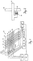
- Fig. 1 illustrates a preferred embodiment of the present invention used in connection with RNA and DNA sequencing. As described hereinbelow, the present invention may also be used for cell detection and antibody detection or detection of any hybridized molecule.
- the sequencer 10 comprises an X-Y array of test sites 12 electronically addressable by conductive leads X1, X2, X3---XN on the X-axis and conductive leads Y1, Y2, Y3---YN on the Y-axis.
- X-logic circuitry 36 for sequentially addressing each X-line is coupled to detection and recognition circuitry 40. Similar circuits 56 are coupled to the Y-lines Y1---YN.
- the array 10 and X and Y logic circuitry 36 and 56 and circuitry 40 may all be implemented on a single semiconductor chip depending upon cost trade-offs.
- the test sites 12, described in greater detail hereinbelow, are formed in a semiconductor wafer using semiconductor photolithographic processing techniques.
- Each test site contains a plurality of probes 22 (See Fig. 4) which are capable of binding to known molecular structures (hereinafter "target(s)").
- the targets could comprise, for example, biopolymers such as polynucleotides, DNA, RNA, cells, antibodies or anti-antibodies.
- the synthetic probes may comprise, for example, oligonucleotides. All the probes 22 in a given test site are identical. But, the probes in respective test sites 12 differ in a known sequence for simultaneous detection of a plurality of different targets (or subsequences within a target molecule) within a single array 10.
- the targets When a sample substance containing the targets in an electrolyte solution 18 is poured onto the array 10, the targets bind with associated probes 22 within a plurality of wells 42 formed in each test site 12. After sufficient time for binding, the surface of the array 10 is rinsed to remove excess targets or other unbound molecular structures. The remaining target structures will be, for the most part, bound to the probes attached to the microfabricated array 10 at specific test sites 12. Each test site 12 is then interrogated electronically by the logic circuitry 36 and 56 to determine whether targets have bound in that test site. Test sites having bound targets, i.e., hybridized molecules, will have changed electrical parameters, which may be detected by detection circuitry 40 coupled to the test sites over the X and Y leads. Thus, by electronic addressing, the detection of specific target/probe bindings is achieved at each test site 12 within the microfabricated array 10, thereby determining the composition of the targets that remain present after washing.
- recognition circuit 40 performs a sequence analysis described in connection with Fig. 21 based upon the composition of the targets (nucleic acids) detected by the circuitry 40.
- Circuit 40 is preferably coupled to the test sites by transistor switches (not shown) using row and column addressing techniques employed, for example, in addressing dynamic random access memory (DRAM) or active matrix liquid crystal display (AMLCD) devices.
- DRAM dynamic random access memory
- AMLCD active matrix liquid crystal display
- the test sites 12 are preferably formed as monolithic structures on a wafer or substrate 34 preferably of single crystal Si or equivalent, such as glass, quartz, alumina etc.
- a resistor array of X and Y resistors 32 coupled to leads RX1, RX2, RX3--- RXN and RY1, RY2, RY3---RYN may be formed by metal evaporation or sputtering of appropriate material on substrate 34.
- the leads are coupled at one end to resistors 32 formed of resistive material, such as nichrome, tungsten or platinum, located beneath each test site and at another end to X-resistor-logic circuit 38 and Y-resistor-logic circuit 58 for probe synthesis purposes to be described later.
- resistors 32 formed of resistive material, such as nichrome, tungsten or platinum, located beneath each test site and at another end to X-resistor-logic circuit 38 and Y-resistor-logic circuit 58 for probe synthesis purposes to be described later.
- resistors 32 may be formed of deposited doped polysilicon, tungsten or tantalum or platinum silicides, nitrides or oxynitrides, by well-known techniques, such as chemical vapor deposition (CVD), molecular beam epitaxy (MBE), metal organic CVD (MOCVD) or similar semiconductor process.
- CVD chemical vapor deposition
- MBE molecular beam epitaxy
- MOCVD metal organic CVD
- a thick (approximately 5000 ⁇ ) SiO 2 film 50 is then formed by CVD on layer 32.
- Figs. 5A-5D only a section of wafer 34 occupied by a single test site 12 is shown. It should be understood that many more, i.e., about 7+ million such sites can be fabricated and tested on a single three inch Si wafer using present state of the art technology.
- the precursor structure shown in the sectional view of Fig. 5A is next processed to form an upper and lower digitated electrode structure, a portion of which is shown in the cross-section IV-IV of Fig. 3, shown in detail in Fig. 4.
- openings 54 are formed in Si 3 N 4 layer 28 by photolithography and reactive ion etching (Fig. 5B).
- Fig. 5C openings 54, about 2 microns wide, are formed in Si 3 N 4 layer 28 by photolithography and reactive ion etching.
- the upper and lower electrodes 21 and 20, respectively, are then formed by successive electron beam evaporation of an adhesion layer (300 ⁇ ) of Ti 26 followed by 2000 ⁇ of contact metallization (Au) 16.
- an adhesion layer 300 ⁇
- Ti 26 titanium
- contact metallization Au
- the lateral edges of the remaining Si 3 N 4 film 28 serve as a precise self-aligning mask for defining the width of the fingers of lower electrode 20, thereby enabling close spacing between the upper and lower electrodes without shorting.
- the electrodes also occupy a relatively large volume of the well, vis-a-vis the volume of the aqueous DNA solution with target DNA 18 (See Fig. 4).
- the spacing between the upper and lower electrodes is of the order of the length (or diameter in solution) of the target DNA molecule. Therefore, the ratio of the target DNA to solvent in the interelectrode space is high, thereby giving greatest sensitivity to the presence or absence of the target DNA during an electrical measurement.
- the length of the electrode fingers is about 100 microns and the width of the set of electrodes is also about 100 microns, with each finger having a width of 2 microns, as shown in Fig. 4 and a spacing of 2 microns.
- the interdigitated design packs a lot of electrode periphery and sample volume in a small area on the wafer. Its ratio of "sample” capacitance to parasitic capacitance caused by leads coming to the site is high.
- Figs. 6A-6F an alternate process for fabricating test sites 12A will be described in connection therewith.
- the layer thicknesses are as indicated in Figs. 5A-5D.
- An SiO 2 layer 50 is grown on a Si substrate 34 (Fig. 6A).
- the SiO 2 film is etched to form an array of 2 micron wide wells 54 periodically spaced from one another by 2 microns (Fig. 6B). Photolithography and reactive ion etching to a depth of about 0.5 microns is used to form the wells 54.
- a poly-Si film 51 of about 2000 ⁇ is formed, for example, by CVD on SiO 2 layer 50 (Fig. 6C).
- the regions of film 51 at the bottom of the well and on the top surfaces is etched away by reactive ion etching (Fig. 6D) leaving sidewalls of polysilicon 51.
- the sidewalls are selectively metallized 51' by silicidation using W, Ti or Pt (Fig. 6E).
- Ni or Au electrodes 61 are formed on the silicide sidewalls 51' by electroless plating (Fig. 6F).
- Figs. 6G and 6H are alternate embodiments of Figs. 6E and 6F respectively.
- the bottom of the test site is textured, in this case by corrugations, to increase the surface area; whereas in Fig. 6H both the electrode 61 and the bottom wall is corrugated. This texturing increases the surface area of a given site, allowing more probes to be attached for greater sensitivity.
- the sensor array 10 described in Figs. 1-4 may, in accordance with the invention, be used as a genosensor to sense the presence or absence of target DNA strands in each test site 12.
- oligonucleotide strands In a decoding test, a large number of relatively short oligonucleotide strands (probes 22) are grown or placed in each test site 12, such that one end of the strand is attached to one or more surfaces of the site.
- the coding sequence of all the strands in a given site 12 is known and is identical, and the coding sequence of each site is different and unique in the array.
- a solution 18 containing long strands of unknown (target) DNA is then washed across the chip. Ideally, the unknown DNA bonds tightly to the oligonucleotide strands 22 in any site that contains the complement to a portion of its own code sequence, but in no other well.
- Methods B, C, D, and E below are designed to measure or detect this difference in ⁇ '' at each site 12. From this data base, a computer "overlapping" or "neural network” algorithm in circuit 40 reconstructs the entire coding sequence of the unknown DNA.
- the AC conductance should be as much as 100 times or more larger than the conductance when no DNA is present.
- Signal loss on a transmission line is also sensitive to ⁇ ''.
- electrical detection of hybridized molecules, such as DNA can be accomplished by scalar measurement of the RF loss of an electromagnetic wave passing along the line 11 at each test site 12A.
- Line 11 may comprise a micro-miniature version of stripline, microstrip, waveguide, coplanar waveguide, slotline, or coaxial line.
- the test site well 42A is made relatively wider and/or longer than the wells in Fig. 4, and the length of the transmission line in the well is maximized by forming it in a meandering pattern.
- a frequency scanned or chirped voltage waveform V i may be applied across the electrodes at each site and the resultant response waveform V o (Fig. 12 or Fig. 13, depending upon whether frequency is increasing or decreasing) is analyzed to determine the presence of hybridized DNA as indicated by a maxima at a hybridized DNA frequency.
- the measurement of the relaxation frequency of the hybridized DNA using a frequency-scanned waveform gives additional information about the properties of the hybridized DNA, e.g., crosslinked versus non-crosslinked.
- a plurality of mechanical resonator structures are formed in test sites formed in silicon wafer 34C, as shown in Fig. 14.
- the resonator structure comprises a lower metal sensor electrode 20C extending in the X-direction and an upper membrane resonator film 21 preferably of silicon nitride or metal such as tantalum extending along a Y-direction in the plane of the wafer.
- the membrane size is about 100 microns in diameter or width/length.
- a dielectric gap 60 preferably of air, is formed between the upper and lower members 21C and 20C.
- a test site well 42C is formed over membrane 16C and probes 22C formed in the well surfaces.
- Target DNA solution 18C is dispensed into the test well 42C.
- the mechanical cavity 60 between the upper and lower electrodes 16C and 20C forms a resonator. This resonator has a resonant frequency in the kilohertz to multimegahertz range with a narrow resonant linewidth.
- Membrane electrode 21C may be formed of a thin film of silicon nitride using chemical vapor deposition at a well controlled silicon to nitrogen ratio and controlled elevated temperature to adjust the film tension when it is cooled to room temperature. Membranes can be formed on unpatterned silicon wafers then released as free standing structures by etching out a silicon window from the back side. Examples of mechanical resonators and details of this construction for use, as above, are given in Buser et al. "Silicon Pressure Sensor Based On a Resonating Element” Sensors and Actuators, A, 25-27 (1991) 717-722 and Prab et al. "Q-Factor and Frequency Shift of Resonating Silicon Diaphragms in Air” Sensors and Actuators A, 25-27 (1991) 691-698.
- a similar class of resonant array detectors can be formed of surface wave devices, for example, by employing surface acoustic waves (SAW) or surface electromagnetic waves.
- SAW surface acoustic waves
- a resonant structure 700 is formed using an acoustic transducer 702 and a SAW reflector 704.
- a scanned frequency wave W from source 708 is launched across the acoustic medium 706 (preferably a lithium niobate or quartz crystal).
- the reflector 704 induces discrete cavity resonances which are detected by measuring, in meter 710, the power dissipated by the transducer. Test sites 712 are formed on the medium.
- Each site may have an associated transducer and reflector or a multiplexer may be formed on the substrate to couple a single transducer to multiple sites.
- Sites with bonded target/probe pairs shift the resonant frequencies. Hence, sites with bonded probes become detectable.
- the transducer 702 may be applied as an interdigitated aluminum thin-film structure evaporated on the lithium niobate crystal substrate 706.
- the reflector 704 can be an aluminum thin-film grating. Standard photolithography and evaporation are used to pattern these structures.
- the phase of the SAW wave after passage through a test site, may be compared in a transmission line to a reference transmission line formed in the substrate and the phase shift caused by bonding used to determine which sites have bonded molecules.
- a monolithically integrated charge-coupled device (CCD) sensor uses optical detection by means of a monolithically integrated charge-coupled device (CCD) sensor to detect the presence or absence of hybridized molecules in a test well.
- CCD charge-coupled device
- Arrays 200 of charge-coupled devices are formed as integrated circuits on silicon wafers 212 to perform an imaging function.
- the CCD array 200 reads-out charge formed beneath detector gate electrodes 220 when light photons (h ⁇ ) impinge on non-hybridized test sites 218A.
- the wavelength of the light (h ⁇ ) is selected to match a known absorption line of one of the hybridized DNA.
- the sensitivity of the method is increased through the use of absorbing dyes such as ethidium bromide which selectively intercalate into hybridized DNA.
- the light passes relatively unattenuated through the non-hybridized test site 218A, but is attenuated by the bound molecules or the dye in the hybridized test sites 218B.
- the light photons induce a charge 223 in the silicon wafer 212 beneath the electrode 220 underlying the non-hybridized wells 218A. Such charges are then read out of the CCD array in the well-known manner and processed to identify the test sites containing hybridized molecules.
- the CCD array genosensor 200 of Fig. 15 is formed by growing a field oxide layer 214 of SiO 2 on a Si epitaxial wafer/substrate 212.
- CCD gate electrodes 220 are then formed by sputtering of metals such as tantalum or tungsten on the oxide 214.
- a dielectric or polymer layer 216 preferably of light transmissive material such as silicon nitride or glass, SiO 2 or polyimide is then formed over the electrodes.
- Wells 230 are then formed in the layer 216 directly above the gate electrodes 220.
- the wells are passivated with a thin protective layer (not shown), such as silicon nitride or aluminum oxide to prevent degradation of the CCD device due to exposure to aqueous solution. Standard lithographic techniques are used to align the gates and wells.
- Probes (not shown) are then formed in the wells 230 to individualize each test site 218 prior to introduction of the aqueous test solution 224.
- the target molecules are tagged with labels using any of the well-known labelling mechanisms, such as fluorescent dyes, radioisotopes or chemiluminescence.
- the CCD array is formed as shown in Fig. 15, with an epitaxial Si substrate 212, a field oxide 214, CCD gates 220, dielectric layer 216 and wells 230.
- the test regions are each provided with unique probes (not shown) and test solutions 224 containing tagged targets.
- the targets may be tagged with luminescent or chemiluminescent or radiological material.
- the test sites containing hybridized tagged DNA emit radiation which is detected by the occurrence of an accumulation of charge in a region beneath a respective CCD gate 220.
- a filter 250 which may be formed of an aluminum or tungsten metal grating or dielectric multilayer interference filter, is formed in the dielectric layer 216 between the well 230 and the metal electrode 220.
- the filter 250 is adapted to block the excitation radiation (h ⁇ ) or ⁇ , ⁇ , ⁇ particles and pass the secondary emission 240.
- the secondary emission is either light or other particles such as electrons stimulated by the excitation.
- the chemiluminescent approach involves the conversion of chemical energy into electromagnetic radiation. Preferred materials are stabilized 1,2-dioxetanes.
- enzyme catalyzed 1,2-dioxetane derivatives can produce a light signal that can last from hours to days.
- the wavelength of emitted light is near 477 nm, and the emission can be controlled by controlling the pH.
- the quantum efficiency of the CCD to be employed is only approximately 13%; thus, the chemiluminescent signal may have to be enhanced.
- Methods of enhancement include the addition of water soluble macromolecules (e.g., bovine serum albumin) to enhance the chemiluminescent signal.
- the probe site array 200' is formed on a separate thin transparent substrate such as a 10-mil-thick pyrex plate 270.
- This separate plate is marked with precision alignment features such as etched or printed gratings (not shown) to permit a precise automated overlay of the separated probe plate onto a separated CCD array 260.
- Each array location in the probe plate is sensitized with unique probes.
- the CCD array is then fabricated with or without the blocking filter 250 of Fig. 15.
- an analysis is made by bringing the probe plate into registered close proximity over the CCD array without using a lens to image the plate onto the CCD. Irradiation of the plate is as in either of the embodiments discussed above in connection with Fig. 15.
- a further alternative is to image the separated probe plate 200' onto the CCD array 260 using a lens. This would allow a greater separation between the plate and the CCD array, for the case in which secondary fluorescence is used, and also allows separation of the excitation and fluorescence by obliquely exciting the probe plate. Imaging with magnification or demagnification is possible so that the probe plate dimensions can be optimized separately from the CCD.
- the CCD device used to monitor the probe array for any of these geometries can be of the conventional variety and sensitive to the ultraviolet and visible spectrum.
- An alternative approach is to use an infrared, heat-sensitive array detector such as a platinum silicide or iridium silicide infrared imager. This latter choice would permit the direct monitoring of heat evolved from the probe array during a biochemical reaction such as hybridization or antibody action. DNA hybridization and other heat-generating reactions may be directly detectable through their thermal signature during reaction.
- the infrared transmission and reflection properties of the product e.g., hybridized DNA
- thermal properties can be monitored also by monitoring thermally generated noise in a conventional visible wavelength or IR detector array.
- heat generated by the biochemical reaction is transmitted by thermal conduction through the thin device layers and detected as a noise burst on the electrode 220.
- the array may also be flood-irradiated with infrared, visible, or ultraviolet light in the configuration of Fig. 15.
- light is chosen specifically in a product-state (e.g., hybridized DNA) absorption band.
- the flood illumination In the unreacted state the flood illumination is transmitted through the well and reflected by filter 250. Wells in which the desired reaction has occurred become absorbing at the flood illumination wavelength. After absorption the flood illumination automatically converts to heat and is detected after conduction into the device below the active well site.
- One method of forming the array 10 uses probes attached to the test sites 12 in the array. Different probes can be attached to the test sites 12 according to the type of target desired. Oligonucleotides, single or double stranded DNA or RNA, antibodies or antigen-antibody complexes, tumor cells and other test probes known to those of skill in the art may be used.
- the probes are attached to the test sites by fixation to a solid support substrate on the surface of the wells 42, or alternatively, attached directly to the electrodes 16 or 20, as in Fig. 4.
- the solid support substrates which can be used to form the surface of the wells 42 include organic or inorganic substrates, such as glass, polystyrenes, polyimides, silicon dioxide, and silicon nitride.
- the solid support substrates or the electrodes must be functionalized to create a surface chemistry conducive to the formation of covalent linkages with the selected probes.
- a glass support can be functionalized with an epoxide group by reaction with an epoxy silane.
- the epoxide group on the support reacts with a 5'-amino-derivatized oligonucleotide probe to form a secondary amine linkage, as described in Parkam and Loudon, BBRC 1:1-6 (1978), which is incorporated by reference herein. Formation of this covalent linkage attaches the probes 26 to the support surface in the desired array.
- Examples of functionalized polystyrene surfaces include 5' aldehyde or carboxylic acid derivatives coupled to hydrazide-activated polystyrene, as described in Kremsky, et al. (1987) Nucl. Acids Res. 15:2891-2909, and 5' amino derivatives coupled to polystyrene which has been activated by diazotization and 5' phosphate derivatives coupled to amino-functionalized polystyrene, as described in Lund, et al. (1988) Nucl. Acids Res. 16:10861-10880, both articles being incorporated by reference herein.
- the electrode surface must be fabricated with materials capable of forming conjugates with the probes.
- Materials which can be incorporated into the surface of the electrodes to provide for direct attachment of probes include electrometal materials, such as gold, niobium oxide, iridium oxide, platinum, titanium, tantalum, tungsten and other metals. These electrometals are capable of forming stable conjugates directly on the plate surface by linkages with organic thiol groups incorporated into the probe, as described in Whitesides et al. (1990) Langmiur 6:87-96 and Hickman et al. (1991) J. Am. Chem. Soc. 113:1128-1132, both of which are incorporated by reference herein.
- a synthetic DNA probe labeled with a thiol group at either the 5' or 3' end will form a stable conjugate with a metal, such as gold, in the plate surface to create an array of directly attached probes.
- the probes in each test site must be uniquely capable of binding to a known molecular or cellular target.
- the probes may be formed (synthesized) off-chip and inserted into each test site by robotic manipulation of micropipettes.
- the probes are linked to gold or SiO 2 or other materials of the test site by means of the linker chemistry described earlier. This method is sufficient to produce low density probe arrays (up to approximately 100 per centimeter).
- the probes may be synthesized in each test site. This method is based upon the fact that key steps of probe synthesis are temperature dependant. By raising the temperature of a surface in a site selective manner, probe chemistry can be directed to specific test sites within an array. This approach is shown in the partial schematic of Fig. 17.
- probes will be synthesized upon an available SiO 2 surface.
- a linker is first attached to the surface.
- test sites are immersed in epoxysilant (fluid A), which covalently links an epoxide to the surface.
- the epoxide is then hydrolyzed and then blocked with trityl chloride, to protect the available primary hydroxyl.
- the array is then immersed in de-protecting solution, typically dilute dichloroacetate in alcohol.
- de-protecting solution typically dilute dichloroacetate in alcohol.
- Laser beam 414, generated by laser 416 is then mechanically scanned across the array by galvanometer scanning system 418.
- the purpose of the laser is to heat the surface at selected test sites.
- Operation of the beam is controlled by logic and switching circuitry 420 which is programmed to irradiate only those test sites 412 where deprotection is desired.
- the de-protecting solution is then removed, thereby revealing free OH groups at sites which were irradiated. Those test sites with free OH groups are now available to add a nucleic acid base.
- DNA probe synthesis can now be performed on the array. Any of the known chemistries can be employed, including phosphoramidite, phosphotriester or hydrogen phosphonate methods.
- the chip is immersed in a solution containing one of the activated based precursors, adenosine (A) for example, and those test sites which had been irradiated in the previous step will link to A.
- A adenosine
- the chip is then re-immersed in de-protecting solution then irradiated again.
- de-protecting solution For example, assume that test sites are irradiated where guanosine (G) is to be attached. After irradiation, activated G is added and the process of synthesizing a second phosphodiester bond is repeated.
- the duty cycle is then performed on the chip for thymidine then cytosine.
- four cycles of irradiation are required to extend the probe array by one nucleic acid subunit.
- forty cycles would be required.
- Laser initiation of the reaction occurs either by localized heating or by photochemistry.
- a preferred embodiment uses a visible-wavelength or UV argon ion laser in combination with a galvanometer scanning system to initiate photochemical synthesis.
- an argon or infrared laser may be used to initiate synthesis by local heating of an array site.
- the method can also be applied to the synthesis of peptides or other polymeric probes on solid supports, based upon the principle of thermally addressable deprotection.
- site selective peptide synthesis is achieved by thermal removal of the f-moc protecting groups, typically in dilute base, followed by capping and the other ordinary steps of peptide synthesis.
- a "glue" layer can be locally activated Fig. 26A-D (or deactivated) or locally applied Fig. 25A-D to a test site by means of scanned laser irradiation.
- the ultraviolet, visible or infrared laser is used to photochemically or thermally alter the adhesion properties of the desired array sites.
- the probe solution for example of type A, is then washed over the array resulting in localized adhesion of the type A probe at the desired sites.
- the type A probe solution is then rapidly rinsed from the system, a second laser irradiation at new array sites is applied, and type B probe solution is introduced to adhere type B probes. The process is repeated to sensitize the full array.
- Array sensitization may be accomplished using, for example, a CW argon-ion or CW Nd:YAG laser using scanning optics such as galvanometers or rotating mirrors, or using a fixed laser beam with a computer-controlled X-Y stage.
- An activation or deactivation process in a "glue” layer can be preferably accomplished using a short-pulsed laser such as a pulsed Nd:YAG laser or excimer laser.
- An excellent approach is to simply cover the "glue” layer 902 to "deprotect” and thereby reveal the "glue” by ablating a passivating material 904 applied over the "glue” (See Figs. 26A-D).
- glucose layers are epoxides, thiols or hydrophilic, e.g., hydrated surfaces.
- Passivating materials can be hydrophobic materials such as fluorine-terminated fluorocarbons or the derivatives or hexamethyldisilizane.
- Figs. 25A-D and 26A-D illustrate two alternate methods of probe formation using the "glue” approach. Furthermore each show two alternate ways to activate a test site.
- a programmable element such as a heater element 906 embedded beneath a test site to induce a thermal reaction in the test site and thereby create or deposit a glue layer 920 to which the probes adhere.
- Fully synthesized probes 912 are washed over the cite and adhere to the exposed glue layer site 920, Fig. 25D.
- Next another site is formed or exposed and a different probe attached.
- external radiation as in Fig. 25B is used to form the glue layer 920; or as in Fig. 26B and C to ablate a passivating layer 904 and expose a glue layer 902.
- an alternative "direct patterning" method may be employed using a stationary illumination beam with a reconfigurable "light-valve” 415 (shown in dotted lines in Fig. 17) such as a liquid-crystal display or switchable mirror array, which is illuminated with a laser or intense lamp.
- the illuminated "light-valve” is imaged onto the sensor array, 400, with a lens system (not shown).
- the pixel elements in the "light-valve” are electronically switched “on” or “off” to select corresponding areas to be sensitized in the sensor array, an excellent "light-valve” device for this purpose is described by J.A. Neff et al. (Proc. of the IEEE, Vol. 78, No. 5, May 1990).
- Another method for synthesizing probe strands uses the embedded resistors 32 described in connection with Figs. 1 and 4 to locally heat predetermined array test sites without substantially heating adjacent sites. This would enable thermally activated synthesis of probes, such as short oligonucleotide strands, to take place in situ in response to application of voltages across selected resistors. Alternatively, high currents would be applied to heat all resistors, except those adjacent to wells where a reaction is desired. In this alternative, the non-synthesized wells are kept at a temperature above the desired synthesis temperature, thereby preventing a synthesis reaction from taking place in these wells.
- the electrically addressable test site array of the invention also provides the ability to electronically induce or catalyze a synthesis reaction in a given well, or row, or column of wells, by applying an electrical potential to the electrodes of such well or wells.
- the potential can be used to attract chemical reactants from solutions disposed near the wells and/or to catalyze a specific chemical reaction in the wells.
- the hybridization between target molecular structures and completed probes can be enhanced by the application of an electrical potential to the electrodes just after the target solution is applied to the test sites. Without the application of a potential, the target molecular structures must diffuse through the solution to the probes. Due to the inefficiency of such a diffusion process, one must allow typically 1.5 to 2 hours for significant hybridization to take place, and even then a substantial number of probes remain unhybridized.
- An electrical potential can draw charged target structures directly to probes near to or attached to the electrodes, increasing both the rate of hybridization and the total number of target/probe hybridizations that can be conveniently produced in a given experiment.
- a reverse biased potential can be subsequently applied to aid in the washing (removal) of unhybridized and mismatched target molecules.
- This technique is not only applicable to the electronic genosensors of Figs. 1 through 9, which have electrodes present within each test site, but can be employed in both the micromechanical-resonator and CCD-based approaches by either using the electrodes present within or under each test site or fabricating one or more additional electrodes at each test site for this purpose.
- the potential applied to individual wells can be used to draw a current surge through the well structure sufficient to evaporate a "glue” layer or glue passivating layer similar to that described above in the last method.
- Sensitization of the array is similar to the electronic programming of an array of electrical fuses.
- reagent sources 352 are individually fluidly coupled via channels L1, L2 --- LN to respective microchannel valves V1,V2 --VN formed in a suitable substrate 341.
- Valves V1-VN enable flow of solution into manifold line L4.
- Microfluidic peristaltic pump P1 forces the solution onto array 10', which is enclosed by laser-radiation-permeable films 344 and 343, such as silicon nitride or silicon dioxide.
- Radiation from laser 416' is selectively projected onto individual test sites 12' formed in substrate 341, in accordance with previously described scanning or imaging methods. Laser scanning of test sites induces localized activation of individual sites as the input solution fluids are rapidly switched using valves V1-VN.
- the entire fluidic system as well as the array may be formed on a single chip of semiconductor or dielectric material, such as Si, glass, Al 2 O 3 , etc.
- Channels 342 are etched into the substrate 341 using conventional photolithography and etchants or by micromachining techniques.
- An array 10' of test sites 12' is formed in the substrate, as described in connection with Figs. 1-6.
- the microfluidic flow system depicted in Figure 19 can be formed as follows.
- a photoresist material is spin-coated on a substrate 341, formed, for example of pyrex glass.
- the microchannel structure is then patterned into the photoresist using standard photolithography and the pattern, including channel structures 343 and 342, are transferred into the substrate by etching using buffered HF.
- a membrane actuator layer 344 comprised of preferably a piezoelectric, such as lead zirconium titanate or PVDF polymer and metal electrodes, is then bonded to the microchannel structure.
- the array 10' is sealed against the microfluidic system preferably using an elastomer O-ring 345.
- Alternate membrane actuator layers known to specialists in the art, make use of shaped memory alloys rather than piezoelectrics, or are based on passive materials deformed electrostatically, for example, aluminum films which are deflected by DC voltages applied to electrodes (not shown).
- Mass production of the flow channel structure is feasible using the photolithographic techniques above.
- laser micromachining techniques such as those developed for etching of silicon in a chlorine ambient.
- a negative-form mold can be made then replicated in positive form, for example, using thermocompression methods.
- Fig. 20 An alternative approach is illustrated in Fig. 20.
- This system is a fast serial microfluidic detector that operates with nanoliter or picoliter solution volumes.
- This system is composed of a microfabricated system of capillary channels and valves V1-VN+3 connected to a main channel C1 and a single (or several ganged) high sensitivity detector array(s) 480 formed as previously described.
- a steady but low-volume stream of a solution containing unknown molecules is mixed using the methods described above in connection with Figs. 18 and 19.
- the unknown solution is sequentially mixed with similarly small volumes of a solution containing known unique batches of oligonucleotide strands from sources S1-SN+3 in a fluidic flow.
- the detector 480 monitors the flow to assess which oligonucleotide batches have reacted with the unknown molecules in a hybridization reaction. Hybridization can be detected, as previously described, either electrically or optically by observing a characteristic shift or distinct spectral feature in the electrical or optical properties of the solution as it flows past the detector.
- An important feature of this system of Figs. 20, 18 and 19 is the use of an extensive channel or capillary network that has minimal dead volumes and fast fluid velocities to allow sequential processing of the flow without diffusion-induced smearing of the batches. This concept is impractical using macroscopic tubing and valves, hence it is preferred to miniaturize such a network.
- FIG. 21 A schematic illustration of the bonding mechanism for sequencing using a synthetic DNA probe is shown in Fig. 21.
- Sequencing by hybridization is a new sequencing approach which exploits the natural base pairing property to provide a recognition mechanism for decoding the nitrogenous bases comprising DNA.
- a partial sequence 802 of a DNA sample is represented on the right.
- Four bases 804 in the sample DNA are specifically paired with a short piece of synthetic DNA 806 attached to a surface.
- the support-bound DNA "probe” serves as a recognition element for the occurrence of a perfectly complementary sequence in the sample"target" DNA 802.
- Example I shows a small portion of the base sequence of a DNA sample, which has been converted to single-stranded form by heating prior to analysis.
- a set of synthetic DNA probes representing all possible sequences for a given probe length (for example, all 65,536 8-base probes)
- a complete list of oligonucleotide sequences contained in the DNA sample can be generated.
- Example 2 below only those 8mer probes listed would hybridize to the sample DNA sequence.
- an overlapping algorithm is used to generate the complete sequence of the target DNA from the oligonucleotide content.
- DNA and RNA detection include genetic research, genetic and infectious disease diagnosis, toxicology testing, individual identification, agriculture identification and breed optimization, quality assurance through contaminant detection, and occupational hazard screening via mutation detection.
- the presence of a defective gene can be detected through the use of simple DNA hybridization detection tests in which a synthetic DNA probe is used to discriminate between a wild type and mutant DNA sequence.
- a substantial DNA sequencing effort is required to search through an entire gene for mutations that may be associated with a disease.
- the sequencer 10 leads to a new gene-targeted DNA sequencing procedure which rapidly detects any mutation within a target gene, facilitating the diagnosis of genetic diseases and identification of carriers, especially when a variety of different mutations may cause the defect.
- the rapid, high throughput nature of the procedure which promises to facilitate population studies aimed at discovering which mutations within a target gene are actually associated with a disease and which mutations represent harmless polymorphisms. This information is expected to lead to simplification of the technology for specific detection of disruptive mutations, and valuable structure-function relationships that facilitate the development of therapeutics.
- the present invention is not limited to genetic diseases; it may be used for rapid,high throughput identification of infectious agents.
- Each species or strain of a virus or micro-organism is predicted to yield a unique, diagnostic pattern of hybridization within an array 10.
- the gene-targeted mutation detection described above will also have important uses in environmental research, for example, the detection of mutations induced by chronic exposure of cells to chemical agents.
- the present invention may be used for individual monitoring of employees who may be exposed to chemicals or radiation in the workplace (e.g., through periodic screening for mutations in populations of circulating lymphocytes).
- An important application of this technology will be the development of a predictive model of mutagenic risk via the characterization of large scale and point mutations in specific genes, such as that for hypoxanthine-quanine phosphoribosyl-transferase (HPRT).
- HPRT hypoxanthine-quanine phosphoribosyl-transferase
- High density arrays will find numerous uses in genome sequencing, and will likely play an important role in the current Human Genome Project (HGP) effort to determine the entire sequence of 3 billion base pairs in the human genome. More importantly, however, are the new human genome projects that will arise because of the availability of fast, high throughput sequencing technology. There will be a need to conduct repetitive DNA sequence analysis of important parts of the human genome derived from large numbers of individuals, in order to characterize complex multi-gene disease conditions and other genetic traits. This activity will persist long after the current HGP is completed and will bring revolutionary progress in biomedical sciences.
- HGP Human Genome Project
- DNA typing is another potential use of the present invention in "DNA typing", in which DNA sequence differences between individuals are analyzed.
- the sequencer of the present invention for simultaneously screening large numbers of polymorphic markers in the DNA of an individual has tremendous advantages over the current technique of restriction fragment length polymorphism (RFLP) analysis, which is time consuming and laborious.
- RFLP restriction fragment length polymorphism
- DNA typing can play an important role in forensics and paternity testing.
- the present invention can be used in connection with detection of targets which are molecular structures other than DNA or RNA, such as cells and antibodies.
- targets which are molecular structures other than DNA or RNA, such as cells and antibodies.
- Table III sets forth feasible probe types for other molecular structures serving as targets. The stated probe types are not meant to be exclusive.
- Probe Types Target Probe DNA, RNA Oligonucleotide Antibody Antigen (peptide), anti-antibody Cell Antibody, protein Hormone receptor Hormone Aviden Biotin Immunoglobulin Protein A Enzyme Enzyme Factor Lectins Specific Carbohydrate
- the detector When the detector employs peptides or other antigens as probes, it can be used to detect antibodies in biological fluids, as shown in Fig. 22.
- a peptide antigen (the probe 22) is affixed to the SiO 2 50 at the bottom of the test well 12A (similar to that illustrated in Fig. 6H), employing a bifunctional crosslinker such as one with a silane at one end and an epoxide or other peptide specific group at the other.
- the treated surface is then incubated with a fluid 18 containing antibody (the target T). Because antibodies are large macromolecules (150,000 to 950,000 MW, depending on class), the resulting target/probe bonding produces a large change in the permittivity of the test well 12A. The magnitude of the effect can be additionally amplified by treating the target/probe complex with a second antibody which is specific for the target antibody, thereby creating a very large complex.
- the commercial application of the methodology is for use to detect the presence of any of hundreds of thousands of different antibodies or other proteins, simultaneously, in a blood sample or other biological fluid. This is particularly useful in blood typing, the detection of viral infection such as AIDS, or the diagnosis of cancer. It would also be very useful as a research tool. It would replace or augment the use of ELISA assays and other biochemical methods to detect antibody/antigen interaction.
- the detector When the detector employs as a probe, peptides, antibodies or other molecules which bind to cells, it can be used to detect specific cell types in biological fluids.
- the probe 22 comprises an antibody, protein or other molecule which is known to bind to the cell surface.
- the target T in this case is an intact cell having receptors T for bonding with the probes 22.
- a fluid solution containing cells is added to the detector. Subsequent to the target/probe binding interaction, binding gives rise to detector wells which are coupled to a cell. Since cells do not conduct current and display low frequency dielectric relaxation, binding of a cell can be detected by either a change in absolute conduction in a well (a modification of the Coulter principle) or by the induction of a low frequency dielectric relaxation effect.
- the commercial application of the methodology is for use to detect the presence of cells with altered cell surface properties, especially cells in the blood or other bodily fluids.
- Cells from solid tissues could be analyzed subsequent to standard tissue dispersement methods.
- Such a detector would be useful in the diagnosis of viral infection and for cancer diagnosis, as well as a scientific research tool. It would serve as a replacement for the use of fluorescence microscopy (immunohistochemistry) and fluorescence activated cell sorting.
- the detection method provides direct detection of target/probe molecular binding. Hence no toxic fluorescent, radioactive, or chemical marker need be attached to the targets or probes. Rather, only an appropriate electrical signal or frequency shift must be experienced for detection. Such signals or shifts naturally occur for many target/probe combinations, such as DNA and RNA to an oligonucleotide. However, if the signal or shift in the electronic detector is weak or nonexistent after bonding, a charged molecular marker can be attached to the target.
- detection in the electronic detector is observed by a change in frequency characteristics, as opposed to a change in magnitude characteristics which can be obscured in time as the microfabricated array is exposed to the corrosive biological solutions.
- the device may be cleaned and reused a number of times without affecting its accuracy.
- a passivation layer can be employed to coat the plates for even longer use.
- Another advantage of the present invention is that the electronic circuitry used to interrogate the test sites to perform the detection measurements can be fabricated directly on the wafer containing the biological array. Switch matrices, signal processing circuitry, and energy sources could all be incorporated on the same chip to facilitate rapid detection across the array. Consequently, the incorporation of active circuitry on the wafer would also greatly reduce the cost of experimentation.
- the density of the probes 22 attached at the test site 12 directly determines the sensitivity.
- the microelectronic method has been shown to provide a factor of ten discrimination between short (nonhybridized) and long (hybridized) single-stranded DNA fragments, whereas the intercalating-dye optical approach provides a factor of three.
- radiographic film reduces the testing time since film exposure is not required.
- Sample preparation time is reduced greatly since the nucleic acid fragments need not be labeled.
- the detection method is quick; the measurements can be performed as soon as sufficient molecular binding is completed.
- the measurement process can be automated via on-chip microprocessor control to provide a very fast method of accessing each test site in the array.
- microelectronic technology incorporated into these types of detection devices will drastically reduce the price for such experimentation.
- efficient mass production techniques employed in making megabit memory chips and megapixel CCD imaging chips can be employed.
- the active circuitry of the genosensor array can be integrated monolithically with the array of wells or the same substrate.
- Switch matrices, analog testing circuits, and analog or digital (microprocessor) controllers could all be fabricated on the same wafer to perform or simplify the electrical tests.
- transistors, such as, TRX 1 could be integrated into each substrate adjacent to a respective test site 12, for example, to disconnect each site electrically, except when it is being sampled. This would necessitate an additional address line A3 for each column but would reduce parasitic capacitance and spurious signals from lines not in use. A greater reduction of these undesired effects could be achieved by a second address line and set of transistors coupled to the Y-side of the site 12.
- CCD circuitry (including CCD implementations of neural networks) has been demonstrated that can perform a wide variety of signal processing and pattern recognition functions. Integration of a CCD data-processing circuit with a genosensor array could simplify the DNA detection and decoding, and would be compatible with the integrated CCD imager, as described in connection with Figs. 15 and 16.
- Embodiments of the invention may include the features of the following enumerated paragraphs ("paras"),
Abstract
Description
- In many applications, it is desirable to detect the presence of one or more molecular structures in a sample. The molecular structures typically comprise ligands, such as, cells, antibodies and anti-antibodies. Ligands are molecules which are recognized by a particular receptor. Ligands may include, without limitation, agonists and antagonists for cell membrane receptors, toxins, venoms, oligo-saccharides, proteins, bacteria, and monoclonal antibodies. For example, a DNA or RNA sequence analysis is very useful in genetic and disease diagnosis, toxicology testing, genetic research, agriculture and pharmaceutical development. Likewise, cell and antibody detection is important in disease diagnosis.
- A number of techniques have been developed for molecular structure detection. In DNA and RNA sequence detection, two procedures are generally used, autoradiography and optical detection. Autoradiography is performed using 32P or 35S. For DNA sequence analysis applications, nucleic acid fragments are end labeled with 32P. These end labeled fragments are separated by size, then exposed to x-ray film for a specified amount of time. The amount of film exposure is directly related to the amount of radioactivity adjacent to a region of film.
- The use of any radioactive label is associated with several disadvantages. First, prolonged exposure to radioactive elements increases the risk of acquiring genetic diseases, such as cancer. As such, precautions must be implemented when using radioactive markers or labels to reduce the exposure to radioactivity. Typically, workers must wear a device to continually monitor radioactive exposure. In addition, pregnant females should take additional precautions to prevent the occurrence of genetic mutations in the unborn.
- The conventional radioactive detection scheme has sensitivity limitations in both the temporal and spatial domains. The use of radioactive labelling currently has a spatial resolution of one millimeter. Additional hardware and software are required to reduce the spatial resolution below one millimeter.
- The sensitivity of detection utilizing autoradiographic film is directly related to the amount of time during which the radioactive labelled fragments are exposed to the film. Thus, the exposure time of the film may range from hours to days, depending upon the level of radioactivity within each detection test site. A β scanner may drastically reduce the time required for film exposure during radiography. However, the use of the β scanner significantly increases the expense associated with this type of detection, and has intrinsically poor spatial resolution.
- Optical detection of fluorescent labelled receptors has also been utilized to detect molecular binding. Briefly, for DNA sequence analysis applications, a base-specific fluorescent dye is attached covalently to the oligonucleotide primers or to the chain terminating dideoxynucleotides used in conjunction with DNA polymerase. The appropriate absorption wavelength for each dye is chosen and used to excite the dye. If the absorption spectra of the dyes are close to each other, a specific wavelength can be chosen to excite the entire set of dyes.
- A particular optical detection technique involves the use of a dye, for example, ethidium bromide, which stains duplexed nucleic acids. The fluorescence of these dyes exhibits an approximate 20-fold increase when it is bound to duplexed DNA or RNA, when compared to the fluorescence exhibited by unbound dye, or dye bound to single-stranded DNA. This type of dye is used to detect the presence of hybridized DNA (or RNA) during a hybridization experiment. Although the use of conventional optical detection methods increases the throughput of the sequencing experiments, the disadvantages are serious.
- Therefore, a need has arisen in the industry for a safe, low-cost, fast and accurate method and apparatus for detecting molecular structures at reduced complexity.
- In accordance with the present invention, a method and apparatus for detecting the presence of molecular structures in predetermined test sites is provided which substantially eliminates or prevents the disadvantages and problems associated with prior devices.
- In an electrical embodiment of the present invention, a substance having a molecular structure is applied to a plurality of test sites, each test site having a probe formed therein capable of binding to a known molecular structure. Electrical signals are applied to the test sites, and electrical properties of the test sites are detected to determine whether the probe has bonded (hybridized) to, or with, an associated molecular structure.
- The test sites are monolithic structures formed on, or in, semiconductor chips or wafers using very large scale integrated (VSLI) circuit methods. This results in a low-cost, small-size, testing device which may be inexpensive enough to be disposable after use.
- Hybridized molecules can be detected, in accordance with one embodiment of the invention, by sensing the change in dissipation of a capacitor formed at the test site, or by sensing the change in AC conductance of a test site when hybridized molecules are present. Alternatively, by forming a transmission line between two electrodes at each test site, the presence of hybridized molecules can be detected by measuring the RF loss associated with the formation of hybridized molecules at the test site.
- In another embodiment, micro-machined resonators are formed in each test site and the change in resonant frequency, or the change in the Quality Factor (Q) of the resonator, caused by formation of hybridized molecules may be measured to determine which sites contain hybridized molecules.
- In an alternate optical embodiment of the invention, a charge-coupled-device (CCD) array is provided, with each electrode of the CCD array aligned with a respective adjacent test site. Light attenuation, caused by greater absorption of illuminating light in test sites with hybridized molecules is used to determine the sites with the hybridized molecules. The CCD array can be integrated with a corresponding test site array. Alternatively the test site array may be a separate disposable plate.
- The probes within each test site are all identical, but differ from test site to test site. The probes for DNA or RNA sequence testing are generally formed of oligonucleotide strands. In accordance with another embodiment of the invention, an optical direct patterning system is used to perform localized sensitization of the microarray or localized synthesis of oligonucleotide strands at each test site to customize or differentiate each of the probe strands.
- A further understanding of the nature and advantages of the invention herein may be realized with respect to the detailed description which follows and the drawings described below.
-
- Fig. 1 is a schematic partial perspective of a microelectronic sensor array in accordance with a preferred embodiment of the invention.
- Fig. 2 is an enlarged view of a portion of Fig. 1.
- Fig. 3 is an enlarged view of the electrode portion of Fig. 2.
- Fig. 4 is a section taken along lines IV-IV of Fig. 3.
- Figs. 5A-5D are schematic cross-sectional process diagrams showing important steps in forming test sites.
- Figs. 6A-6H are schematic cross-sectional process diagrams showing important steps in forming alternate embodiments of the test sites.
- Fig. 7 is a plot of dissipation factor versus frequency for bonded test sites (Curve A) and unbonded test sites (Curve B).
- Fig. 8 is a plan view of an alternate test site embodiment using a meander transmission line.
- Fig. 9 is a schematic of a test site detection system using an applied AC input voltage Vi having a frequency range f1 to f2.
- Fig. 10 is a plot of the AC conductance of the test site to the input voltage Vi.
- Fig. 11 is a plot of Vi versus time for a constant amplitude signal which is swept from a lower frequency f1 to a higher frequency f2.
- Fig. 12 is a plot of the sensed output voltage Vo from the test site in response to the input voltage waveform of Fig. 11.
- Fig. 13 is a plot of the sensed output voltage Vo from the test site in response to an input waveform Vi which descends from f2 to f1.
- Fig. 14 is a schematic sectional view of a test site fabricated with a mechanical resonator structure.
- Fig. 15 is a schematic cross-section of an alternate embodiment in which the test sites are formed with an underlying CCD array.
- Fig. 16 is a view as in Fig. 15 wherein the test sites are formed in a disposable plate and associated with a separable CCD array .
- Fig. 17 is a schematic view of a system for synthesizing probes in the test sites.
- Fig. 18 is a schematic illustration of a microfluidic system for synthesizing probes in situ.
- Fig. 19 is a schematic cross-section of the microfluidic system of Fig. 18.
- Fig. 20 is a schematic of a microfluidic genosensor embodiment.
- Fig. 21 is a schematic illustration of the method whereby a synthetic DNA probe selectively binds to a predetermined DNA sequence.
- Fig. 22 is a schematic cross-section of a test well used to detect molecules in biological fluids.
- Fig. 23 is a schematic representation of a surface-acoustic-wave embodiment of the invention.
- Fig. 24 is a partial schematic of an alternative addressing embodiment of the invention.
- Fig. 25A-D is a series of cross-sectional drawings illustrating an alternate method of array sensitization.
- Fig. 26A-D is a series as in Fig. 25A-D depicting an alternative array sensitization method.
-
- A preferred embodiment of the present invention and its advantages may be understood by referring to Figs. 1-4 and 4A-4C of the drawings, in which like numerals are used for like and corresponding parts of the various drawings.
- Fig. 1 illustrates a preferred embodiment of the present invention used in connection with RNA and DNA sequencing. As described hereinbelow, the present invention may also be used for cell detection and antibody detection or detection of any hybridized molecule.
- The
sequencer 10 comprises an X-Y array oftest sites 12 electronically addressable by conductive leads X1, X2, X3---XN on the X-axis and conductive leads Y1, Y2, Y3---YN on the Y-axis.X-logic circuitry 36 for sequentially addressing each X-line is coupled to detection andrecognition circuitry 40.Similar circuits 56 are coupled to the Y-lines Y1---YN. Thearray 10 and X andY logic circuitry circuitry 40 may all be implemented on a single semiconductor chip depending upon cost trade-offs. - The
test sites 12, described in greater detail hereinbelow, are formed in a semiconductor wafer using semiconductor photolithographic processing techniques. Each test site contains a plurality of probes 22 (See Fig. 4) which are capable of binding to known molecular structures (hereinafter "target(s)"). The targets could comprise, for example, biopolymers such as polynucleotides, DNA, RNA, cells, antibodies or anti-antibodies. For the case of a RNA or DNA sequencer, the synthetic probes may comprise, for example, oligonucleotides. All theprobes 22 in a given test site are identical. But, the probes inrespective test sites 12 differ in a known sequence for simultaneous detection of a plurality of different targets (or subsequences within a target molecule) within asingle array 10. - When a sample substance containing the targets in an
electrolyte solution 18 is poured onto thearray 10, the targets bind with associatedprobes 22 within a plurality ofwells 42 formed in eachtest site 12. After sufficient time for binding, the surface of thearray 10 is rinsed to remove excess targets or other unbound molecular structures. The remaining target structures will be, for the most part, bound to the probes attached to themicrofabricated array 10 atspecific test sites 12. Eachtest site 12 is then interrogated electronically by thelogic circuitry detection circuitry 40 coupled to the test sites over the X and Y leads. Thus, by electronic addressing, the detection of specific target/probe bindings is achieved at eachtest site 12 within themicrofabricated array 10, thereby determining the composition of the targets that remain present after washing. - For the example of DNA sequencing,
recognition circuit 40 performs a sequence analysis described in connection with Fig. 21 based upon the composition of the targets (nucleic acids) detected by thecircuitry 40. - Note:
Circuit 40 is preferably coupled to the test sites by transistor switches (not shown) using row and column addressing techniques employed, for example, in addressing dynamic random access memory (DRAM) or active matrix liquid crystal display (AMLCD) devices. - The
test sites 12 are preferably formed as monolithic structures on a wafer orsubstrate 34 preferably of single crystal Si or equivalent, such as glass, quartz, alumina etc. First, an optional resistor array of X andY resistors 32 coupled to leads RX1, RX2, RX3--- RXN and RY1, RY2, RY3---RYN (as shown in Fig. 1) may be formed by metal evaporation or sputtering of appropriate material onsubstrate 34. The leads are coupled at one end toresistors 32 formed of resistive material, such as nichrome, tungsten or platinum, located beneath each test site and at another end to X-resistor-logic circuit 38 and Y-resistor-logic circuit 58 for probe synthesis purposes to be described later. - Alternatively,
resistors 32 may be formed of deposited doped polysilicon, tungsten or tantalum or platinum silicides, nitrides or oxynitrides, by well-known techniques, such as chemical vapor deposition (CVD), molecular beam epitaxy (MBE), metal organic CVD (MOCVD) or similar semiconductor process. - Referring to Figs. 5A-5D, after the
resistors 32 and resistors RX and RY address lines are formed, a thick (approximately 5000Å) SiO2 film 50 is then formed by CVD onlayer 32. Athin layer 28 of about 500 Å of a mask material, such as Si3N4, is then formed on SiO2 film 50, for example by Chemical Vapor Deposition (CVD) (Fig. 5A). - NOTE: In Figs. 5A-5D, only a section of
wafer 34 occupied by asingle test site 12 is shown. It should be understood that many more, i.e., about 7+ million such sites can be fabricated and tested on a single three inch Si wafer using present state of the art technology. - The precursor structure shown in the sectional view of Fig. 5A is next processed to form an upper and lower digitated electrode structure, a portion of which is shown in the cross-section IV-IV of Fig. 3, shown in detail in Fig. 4.
- First,
openings 54, about 2 microns wide, are formed in Si3N4 layer 28 by photolithography and reactive ion etching (Fig. 5B). Next, about 4000 Å of SiO2 layer 50 is wet etched with an acid solution, such as buffered HF, to form recesses 54' (Fig. 5C). - The upper and
lower electrodes Ti 26 followed by 2000 Å of contact metallization (Au) 16. Note that the lateral edges of the remaining Si3N4 film 28 serve as a precise self-aligning mask for defining the width of the fingers oflower electrode 20, thereby enabling close spacing between the upper and lower electrodes without shorting. Hence, the well sites can be tested at low applied voltages. The electrodes also occupy a relatively large volume of the well, vis-a-vis the volume of the aqueous DNA solution with target DNA 18 (See Fig. 4). Most importantly, the spacing between the upper and lower electrodes is of the order of the length (or diameter in solution) of the target DNA molecule. Therefore, the ratio of the target DNA to solvent in the interelectrode space is high, thereby giving greatest sensitivity to the presence or absence of the target DNA during an electrical measurement. - The length of the electrode fingers, as shown in Fig. 3 and Fig. 5A, is about 100 microns and the width of the set of electrodes is also about 100 microns, with each finger having a width of 2 microns, as shown in Fig. 4 and a spacing of 2 microns.
- The interdigitated design packs a lot of electrode periphery and sample volume in a small area on the wafer. Its ratio of "sample" capacitance to parasitic capacitance caused by leads coming to the site is high.
- Referring now to the schematic sectioned sequence views of Figs. 6A-6F, an alternate process for fabricating
test sites 12A will be described in connection therewith. Note: Unless specified, the layer thicknesses are as indicated in Figs. 5A-5D. An SiO2 layer 50 is grown on a Si substrate 34 (Fig. 6A). The SiO2 film is etched to form an array of 2 micronwide wells 54 periodically spaced from one another by 2 microns (Fig. 6B). Photolithography and reactive ion etching to a depth of about 0.5 microns is used to form thewells 54. A poly-Si film 51 of about 2000Å is formed, for example, by CVD on SiO2 layer 50 (Fig. 6C). The regions offilm 51 at the bottom of the well and on the top surfaces is etched away by reactive ion etching (Fig. 6D) leaving sidewalls ofpolysilicon 51. The sidewalls are selectively metallized 51' by silicidation using W, Ti or Pt (Fig. 6E). Finally, Ni orAu electrodes 61 are formed on the silicide sidewalls 51' by electroless plating (Fig. 6F). - Figs. 6G and 6H are alternate embodiments of Figs. 6E and 6F respectively. In Fig. 6G the bottom of the test site is textured, in this case by corrugations, to increase the surface area; whereas in Fig. 6H both the
electrode 61 and the bottom wall is corrugated. This texturing increases the surface area of a given site, allowing more probes to be attached for greater sensitivity. - The
sensor array 10 described in Figs. 1-4 may, in accordance with the invention, be used as a genosensor to sense the presence or absence of target DNA strands in eachtest site 12. - In a decoding test, a large number of relatively short oligonucleotide strands (probes 22) are grown or placed in each
test site 12, such that one end of the strand is attached to one or more surfaces of the site. The coding sequence of all the strands in a givensite 12 is known and is identical, and the coding sequence of each site is different and unique in the array. Asolution 18 containing long strands of unknown (target) DNA is then washed across the chip. Ideally, the unknown DNA bonds tightly to theoligonucleotide strands 22 in any site that contains the complement to a portion of its own code sequence, but in no other well. Practically, some weakly bound target mismatches may occur, but these can be alleviated by rinsing the well with an appropriate solution at an appropriate ion concentration and temperature. Consequently, after a rinse, a number of the wells in the array will contain a significant amount of this bonded or hybridized DNA, and the rest will contain only the original oligonucleotide strands in an aqueous solution. The wells are then interrogated electrically in sequence using theelectrodes site 12. From this data base, a computer "overlapping" or "neural network" algorithm incircuit 40 reconstructs the entire coding sequence of the unknown DNA. - Fig. 7 is a plot of dissipation factor versus the log of frequency for bonded (hybridized) DNA (curve B) and unbonded DNA (curve A) showing how the dispersion factor D = ∈"/∈' differs, depending upon whether the DNA is bonded or not. Note: Depending upon the particular samples measured, the curves of Fig. 7 may be reversed, i.e. curve B could represent unbonded DNA. This difference in dispersion factor is used to determine the presence or absence of hybridized DNA at a test site formed as in Figs. 1-6. The dissipation factor at each test site is measured by well-known instrumentation such as an LCR meter in
circuit 40. The meter is successively coupled to eachsite 12 vialogic circuits - Similarly, the presence or absence of hybridized DNA can be detected by measuring the AC conductance GAC = ∈"A/d at each test site; wherein A is the effective area of one electrode and d is the effective distance between electrodes. At the relaxation frequency of a given DNA molecule, the AC conductance should be as much as 100 times or more larger than the conductance when no DNA is present. Fig. 9 is a schematic representation of how this test may be conducted. A pulsed or frequency-scanned waveform is applied across electrodes 21B and 20B of each test site 12B.
Probes 22 are formed on each electrode and an aqueous solution of target molecules is formed in thewells 42B of the test sites 12B. The presence of hybridized DNA is detected at a resonant frequency of DNA as shown in Fig. 10.
An LCR meter may be used to measure G or R = 1/G at a discrete frequency. Alternatively, as discussed in connection with Figs. 9 and 10, G can be measured as a function of frequency. - Signal loss on a transmission line is also sensitive to ∈''. By incorporating a
transmission line 11 between the X and Y lines at each test site (as shown in Fig. 8) electrical detection of hybridized molecules, such as DNA, can be accomplished by scalar measurement of the RF loss of an electromagnetic wave passing along theline 11 at eachtest site 12A.Line 11 may comprise a micro-miniature version of stripline, microstrip, waveguide, coplanar waveguide, slotline, or coaxial line. To achieve maximum sensitivity with this method, the test site well 42A is made relatively wider and/or longer than the wells in Fig. 4, and the length of the transmission line in the well is maximized by forming it in a meandering pattern. - As shown in Fig. 11, a frequency scanned or chirped voltage waveform Vi may be applied across the electrodes at each site and the resultant response waveform Vo (Fig. 12 or Fig. 13, depending upon whether frequency is increasing or decreasing) is analyzed to determine the presence of hybridized DNA as indicated by a maxima at a hybridized DNA frequency. The measurement of the relaxation frequency of the hybridized DNA using a frequency-scanned waveform gives additional information about the properties of the hybridized DNA, e.g., crosslinked versus non-crosslinked.
- In this embodiment, a plurality of mechanical resonator structures are formed in test sites formed in
silicon wafer 34C, as shown in Fig. 14. The resonator structure comprises a lowermetal sensor electrode 20C extending in the X-direction and an uppermembrane resonator film 21 preferably of silicon nitride or metal such as tantalum extending along a Y-direction in the plane of the wafer. Typically the membrane size is about 100 microns in diameter or width/length. Adielectric gap 60, preferably of air, is formed between the upper andlower members - A test site well 42C is formed over membrane 16C and probes 22C formed in the well surfaces.
Target DNA solution 18C is dispensed into thetest well 42C. Themechanical cavity 60 between the upper andlower electrodes 16C and 20C forms a resonator. This resonator has a resonant frequency in the kilohertz to multimegahertz range with a narrow resonant linewidth. - An RF signal propagated across each resonator will produce a characteristic high Q response with a narrow linewidth. A shift in either Q or resonant frequency indicates the presence of hybridized molecules on the resonator
surface electrode membrane 21C. -
Membrane electrode 21C may be formed of a thin film of silicon nitride using chemical vapor deposition at a well controlled silicon to nitrogen ratio and controlled elevated temperature to adjust the film tension when it is cooled to room temperature. Membranes can be formed on unpatterned silicon wafers then released as free standing structures by etching out a silicon window from the back side. Examples of mechanical resonators and details of this construction for use, as above, are given in Buser et al. "Silicon Pressure Sensor Based On a Resonating Element" Sensors and Actuators, A, 25-27 (1991) 717-722 and Prab et al. "Q-Factor and Frequency Shift of Resonating Silicon Diaphragms in Air" Sensors and Actuators A, 25-27 (1991) 691-698. - A similar class of resonant array detectors can be formed of surface wave devices, for example, by employing surface acoustic waves (SAW) or surface electromagnetic waves. In the case of a SAW detector, as shown in Fig. 23, a
resonant structure 700 is formed using anacoustic transducer 702 and aSAW reflector 704. A scanned frequency wave W fromsource 708 is launched across the acoustic medium 706 (preferably a lithium niobate or quartz crystal). Thereflector 704 induces discrete cavity resonances which are detected by measuring, inmeter 710, the power dissipated by the transducer. Test sites 712 are formed on the medium. Each site may have an associated transducer and reflector or a multiplexer may be formed on the substrate to couple a single transducer to multiple sites. Sites with bonded target/probe pairs shift the resonant frequencies. Hence, sites with bonded probes become detectable. Thetransducer 702 may be applied as an interdigitated aluminum thin-film structure evaporated on the lithiumniobate crystal substrate 706. Thereflector 704 can be an aluminum thin-film grating. Standard photolithography and evaporation are used to pattern these structures. - Alternatively, the phase of the SAW wave, after passage through a test site, may be compared in a transmission line to a reference transmission line formed in the substrate and the phase shift caused by bonding used to determine which sites have bonded molecules.
- Referring now to the cross-sectional schematic view of Fig. 15, an alternate embodiment of the invention will now be described which uses optical detection by means of a monolithically integrated charge-coupled device (CCD) sensor to detect the presence or absence of hybridized molecules in a test well.
-
Arrays 200 of charge-coupled devices (CCD's) are formed as integrated circuits onsilicon wafers 212 to perform an imaging function. TheCCD array 200 reads-out charge formed beneathdetector gate electrodes 220 when light photons (hυ) impinge onnon-hybridized test sites 218A. - The wavelength of the light (hυ) is selected to match a known absorption line of one of the hybridized DNA. The sensitivity of the method is increased through the use of absorbing dyes such as ethidium bromide which selectively intercalate into hybridized DNA. The light passes relatively unattenuated through the
non-hybridized test site 218A, but is attenuated by the bound molecules or the dye in the hybridizedtest sites 218B. - The light photons induce a
charge 223 in thesilicon wafer 212 beneath theelectrode 220 underlying thenon-hybridized wells 218A. Such charges are then read out of the CCD array in the well-known manner and processed to identify the test sites containing hybridized molecules. - The
CCD array genosensor 200 of Fig. 15 is formed by growing afield oxide layer 214 of SiO2 on a Si epitaxial wafer/substrate 212.CCD gate electrodes 220 are then formed by sputtering of metals such as tantalum or tungsten on theoxide 214. A dielectric orpolymer layer 216, preferably of light transmissive material such as silicon nitride or glass, SiO2 or polyimide is then formed over the electrodes.Wells 230 are then formed in thelayer 216 directly above thegate electrodes 220. The wells are passivated with a thin protective layer (not shown), such as silicon nitride or aluminum oxide to prevent degradation of the CCD device due to exposure to aqueous solution. Standard lithographic techniques are used to align the gates and wells. - Probes (not shown) are then formed in the
wells 230 to individualize eachtest site 218 prior to introduction of theaqueous test solution 224. - In an alternative embodiment, the target molecules are tagged with labels using any of the well-known labelling mechanisms, such as fluorescent dyes, radioisotopes or chemiluminescence. The CCD array is formed as shown in Fig. 15, with an
epitaxial Si substrate 212, afield oxide 214,CCD gates 220,dielectric layer 216 andwells 230. - The test regions are each provided with unique probes (not shown) and
test solutions 224 containing tagged targets. The targets may be tagged with luminescent or chemiluminescent or radiological material. The test sites containing hybridized tagged DNA emit radiation which is detected by the occurrence of an accumulation of charge in a region beneath arespective CCD gate 220. - Preferably, in the labelled target embodiment a
filter 250, which may be formed of an aluminum or tungsten metal grating or dielectric multilayer interference filter, is formed in thedielectric layer 216 between the well 230 and themetal electrode 220. Thefilter 250 is adapted to block the excitation radiation (hυ) or α, β, γ particles and pass thesecondary emission 240. The secondary emission is either light or other particles such as electrons stimulated by the excitation. The chemiluminescent approach involves the conversion of chemical energy into electromagnetic radiation. Preferred materials are stabilized 1,2-dioxetanes. Unlike other chemiluminescent modalities, enzyme catalyzed 1,2-dioxetane derivatives can produce a light signal that can last from hours to days. The wavelength of emitted light is near 477 nm, and the emission can be controlled by controlling the pH. At 477 nm, the quantum efficiency of the CCD to be employed is only approximately 13%; thus, the chemiluminescent signal may have to be enhanced. Methods of enhancement include the addition of water soluble macromolecules (e.g., bovine serum albumin) to enhance the chemiluminescent signal. - The advantages for using 1,2-dioxetanes are numerous. In addition to no radioactivity exposure, this method is relatively simple to perform (reagents and equipment are inexpensive). Finally, this method has a low background noise level and wide dynamic range.
- In an alternative two-piece implementation as shown in Fig. 16 the probe site array 200' is formed on a separate thin transparent substrate such as a 10-mil-
thick pyrex plate 270. This separate plate is marked with precision alignment features such as etched or printed gratings (not shown) to permit a precise automated overlay of the separated probe plate onto a separatedCCD array 260. Each array location in the probe plate is sensitized with unique probes. The CCD array is then fabricated with or without the blockingfilter 250 of Fig. 15. In one embodiment, an analysis is made by bringing the probe plate into registered close proximity over the CCD array without using a lens to image the plate onto the CCD. Irradiation of the plate is as in either of the embodiments discussed above in connection with Fig. 15. A further alternative is to image the separated probe plate 200' onto theCCD array 260 using a lens. This would allow a greater separation between the plate and the CCD array, for the case in which secondary fluorescence is used, and also allows separation of the excitation and fluorescence by obliquely exciting the probe plate. Imaging with magnification or demagnification is possible so that the probe plate dimensions can be optimized separately from the CCD. - The CCD device used to monitor the probe array for any of these geometries can be of the conventional variety and sensitive to the ultraviolet and visible spectrum. An alternative approach is to use an infrared, heat-sensitive array detector such as a platinum silicide or iridium silicide infrared imager. This latter choice would permit the direct monitoring of heat evolved from the probe array during a biochemical reaction such as hybridization or antibody action. DNA hybridization and other heat-generating reactions may be directly detectable through their thermal signature during reaction. The infrared transmission and reflection properties of the product (e.g., hybridized DNA) will be distinctly different than the reactants due to the formation of new molecular bonds with new absorptions from infrared-active vibrational and rotational modes in the product molecule. In the configuration of Figs. 15 and 16, thermal properties can be monitored also by monitoring thermally generated noise in a conventional visible wavelength or IR detector array. In this case heat generated by the biochemical reaction is transmitted by thermal conduction through the thin device layers and detected as a noise burst on the
electrode 220. The array may also be flood-irradiated with infrared, visible, or ultraviolet light in the configuration of Fig. 15. In this case, light is chosen specifically in a product-state (e.g., hybridized DNA) absorption band. In the unreacted state the flood illumination is transmitted through the well and reflected byfilter 250. Wells in which the desired reaction has occurred become absorbing at the flood illumination wavelength. After absorption the flood illumination automatically converts to heat and is detected after conduction into the device below the active well site. - One method of forming the
array 10 uses probes attached to thetest sites 12 in the array. Different probes can be attached to thetest sites 12 according to the type of target desired. Oligonucleotides, single or double stranded DNA or RNA, antibodies or antigen-antibody complexes, tumor cells and other test probes known to those of skill in the art may be used. The probes are attached to the test sites by fixation to a solid support substrate on the surface of thewells 42, or alternatively, attached directly to theelectrodes wells 42 include organic or inorganic substrates, such as glass, polystyrenes, polyimides, silicon dioxide, and silicon nitride. - The solid support substrates or the electrodes must be functionalized to create a surface chemistry conducive to the formation of covalent linkages with the selected probes. As an example, a glass support can be functionalized with an epoxide group by reaction with an epoxy silane. The epoxide group on the support reacts with a 5'-amino-derivatized oligonucleotide probe to form a secondary amine linkage, as described in Parkam and Loudon, BBRC 1:1-6 (1978), which is incorporated by reference herein. Formation of this covalent linkage attaches the
probes 26 to the support surface in the desired array. Examples of functionalized polystyrene surfaces include 5' aldehyde or carboxylic acid derivatives coupled to hydrazide-activated polystyrene, as described in Kremsky, et al. (1987) Nucl. Acids Res. 15:2891-2909, and 5' amino derivatives coupled to polystyrene which has been activated by diazotization and 5' phosphate derivatives coupled to amino-functionalized polystyrene, as described in Lund, et al. (1988) Nucl. Acids Res. 16:10861-10880, both articles being incorporated by reference herein. - For direct attachment of probes to the electrodes, the electrode surface must be fabricated with materials capable of forming conjugates with the probes. Materials which can be incorporated into the surface of the electrodes to provide for direct attachment of probes include electrometal materials, such as gold, niobium oxide, iridium oxide, platinum, titanium, tantalum, tungsten and other metals. These electrometals are capable of forming stable conjugates directly on the plate surface by linkages with organic thiol groups incorporated into the probe, as described in Whitesides et al. (1990) Langmiur 6:87-96 and Hickman et al. (1991) J. Am. Chem. Soc. 113:1128-1132, both of which are incorporated by reference herein. As an example, a synthetic DNA probe labeled with a thiol group at either the 5' or 3' end will form a stable conjugate with a metal, such as gold, in the plate surface to create an array of directly attached probes.
- The probes in each test site must be uniquely capable of binding to a known molecular or cellular target. The probes may be formed (synthesized) off-chip and inserted into each test site by robotic manipulation of micropipettes. In this embodiment, the probes are linked to gold or SiO2 or other materials of the test site by means of the linker chemistry described earlier. This method is sufficient to produce low density probe arrays (up to approximately 100 per centimeter).
- Alternatively, the probes may be synthesized in each test site. This method is based upon the fact that key steps of probe synthesis are temperature dependant. By raising the temperature of a surface in a site selective manner, probe chemistry can be directed to specific test sites within an array. This approach is shown in the partial schematic of Fig. 17.
- As an example of this embodiment, an
array 400 oftest sites 412 formed as previously shown in Figs. 1-4. In one embodiment of this approach, probes will be synthesized upon an available SiO2 surface. In order to begin probe synthesis, a linker is first attached to the surface. To achieve linker attachment, test sites are immersed in epoxysilant (fluid A), which covalently links an epoxide to the surface. The epoxide is then hydrolyzed and then blocked with trityl chloride, to protect the available primary hydroxyl. - In order to begin probe synthesis, the array is then immersed in de-protecting solution, typically dilute dichloroacetate in alcohol.
Laser beam 414, generated bylaser 416 is then mechanically scanned across the array bygalvanometer scanning system 418. The purpose of the laser is to heat the surface at selected test sites. Operation of the beam is controlled by logic and switchingcircuitry 420 which is programmed to irradiate only thosetest sites 412 where deprotection is desired. After irradiation, the de-protecting solution is then removed, thereby revealing free OH groups at sites which were irradiated. Those test sites with free OH groups are now available to add a nucleic acid base. - DNA probe synthesis can now be performed on the array. Any of the known chemistries can be employed, including phosphoramidite, phosphotriester or hydrogen phosphonate methods. The chip is immersed in a solution containing one of the activated based precursors, adenosine (A) for example, and those test sites which had been irradiated in the previous step will link to A.
- Following the standard phosphodiester chemistry, as generally employed for oligonucleotide synthesis, the chip is then re-immersed in de-protecting solution then irradiated again. For example, assume that test sites are irradiated where guanosine (G) is to be attached. After irradiation, activated G is added and the process of synthesizing a second phosphodiester bond is repeated.
- The duty cycle is then performed on the chip for thymidine then cytosine. In all, because there are four nucleic acid bases, four cycles of irradiation are required to extend the probe array by one nucleic acid subunit. To synthesize an array of ten-base-long probes, forty cycles would be required.
- Laser initiation of the reaction occurs either by localized heating or by photochemistry. A preferred embodiment uses a visible-wavelength or UV argon ion laser in combination with a galvanometer scanning system to initiate photochemical synthesis. Alternatively, since synthesis reactions are known to be highly temperature sensitive, an argon or infrared laser may be used to initiate synthesis by local heating of an array site.
- The method can also be applied to the synthesis of peptides or other polymeric probes on solid supports, based upon the principle of thermally addressable deprotection. For example, in the case of peptide synthesis, site selective peptide synthesis is achieved by thermal removal of the f-moc protecting groups, typically in dilute base, followed by capping and the other ordinary steps of peptide synthesis.
- Alternatively, a "glue" layer can be locally activated Fig. 26A-D (or deactivated) or locally applied Fig. 25A-D to a test site by means of scanned laser irradiation. In this embodiment the ultraviolet, visible or infrared laser is used to photochemically or thermally alter the adhesion properties of the desired array sites. The probe solution, for example of type A, is then washed over the array resulting in localized adhesion of the type A probe at the desired sites. The type A probe solution is then rapidly rinsed from the system, a second laser irradiation at new array sites is applied, and type B probe solution is introduced to adhere type B probes. The process is repeated to sensitize the full array.
- Array sensitization may be accomplished using, for example, a CW argon-ion or CW Nd:YAG laser using scanning optics such as galvanometers or rotating mirrors, or using a fixed laser beam with a computer-controlled X-Y stage. An activation or deactivation process in a "glue" layer can be preferably accomplished using a short-pulsed laser such as a pulsed Nd:YAG laser or excimer laser. An excellent approach is to simply cover the "glue"
layer 902 to "deprotect" and thereby reveal the "glue" by ablating apassivating material 904 applied over the "glue" (See Figs. 26A-D). Examples of "glue" layers are epoxides, thiols or hydrophilic, e.g., hydrated surfaces. Passivating materials can be hydrophobic materials such as fluorine-terminated fluorocarbons or the derivatives or hexamethyldisilizane. - Figs. 25A-D and 26A-D illustrate two alternate methods of probe formation using the "glue" approach. Furthermore each show two alternate ways to activate a test site. One way is to use a programmable element such as a
heater element 906 embedded beneath a test site to induce a thermal reaction in the test site and thereby create or deposit aglue layer 920 to which the probes adhere. Fully synthesizedprobes 912 are washed over the cite and adhere to the exposedglue layer site 920, Fig. 25D. Next another site is formed or exposed and a different probe attached. Alternatively external radiation as in Fig. 25B is used to form theglue layer 920; or as in Fig. 26B and C to ablate apassivating layer 904 and expose aglue layer 902. - In addition to the use of a scanned laser beam, an alternative "direct patterning" method may be employed using a stationary illumination beam with a reconfigurable "light-valve" 415 (shown in dotted lines in Fig. 17) such as a liquid-crystal display or switchable mirror array, which is illuminated with a laser or intense lamp. The illuminated "light-valve" is imaged onto the sensor array, 400, with a lens system (not shown). The pixel elements in the "light-valve" are electronically switched "on" or "off" to select corresponding areas to be sensitized in the sensor array, an excellent "light-valve" device for this purpose is described by J.A. Neff et al. (Proc. of the IEEE, Vol. 78, No. 5, May 1990).
- Another approach to on-chip synthesis of probes is described in PCT International Publication Number WO 90/15070, entitled "Very Large Scale Immobilized Peptide Synthesis" to Pirrung et al., assigned to Affymax Technologies, having an International Publication Date of December 13, 1990, which is incorporated by reference herein. This approach is based upon laser directed photochemistry of protecting groups, rather than site directed thermal chemistry or surfaces.
- Another method for synthesizing probe strands uses the embedded
resistors 32 described in connection with Figs. 1 and 4 to locally heat predetermined array test sites without substantially heating adjacent sites. This would enable thermally activated synthesis of probes, such as short oligonucleotide strands, to take place in situ in response to application of voltages across selected resistors. Alternatively, high currents would be applied to heat all resistors, except those adjacent to wells where a reaction is desired. In this alternative, the non-synthesized wells are kept at a temperature above the desired synthesis temperature, thereby preventing a synthesis reaction from taking place in these wells. - The electrically addressable test site array of the invention also provides the ability to electronically induce or catalyze a synthesis reaction in a given well, or row, or column of wells, by applying an electrical potential to the electrodes of such well or wells.
- The potential can be used to attract chemical reactants from solutions disposed near the wells and/or to catalyze a specific chemical reaction in the wells.
- Furthermore, the hybridization between target molecular structures and completed probes can be enhanced by the application of an electrical potential to the electrodes just after the target solution is applied to the test sites. Without the application of a potential, the target molecular structures must diffuse through the solution to the probes. Due to the inefficiency of such a diffusion process, one must allow typically 1.5 to 2 hours for significant hybridization to take place, and even then a substantial number of probes remain unhybridized. An electrical potential can draw charged target structures directly to probes near to or attached to the electrodes, increasing both the rate of hybridization and the total number of target/probe hybridizations that can be conveniently produced in a given experiment. Conversely, a reverse biased potential can be subsequently applied to aid in the washing (removal) of unhybridized and mismatched target molecules. This technique is not only applicable to the electronic genosensors of Figs. 1 through 9, which have electrodes present within each test site, but can be employed in both the micromechanical-resonator and CCD-based approaches by either using the electrodes present within or under each test site or fabricating one or more additional electrodes at each test site for this purpose.
- Alternatively, the potential applied to individual wells can be used to draw a current surge through the well structure sufficient to evaporate a "glue" layer or glue passivating layer similar to that described above in the last method. Sensitization of the array is similar to the electronic programming of an array of electrical fuses.
- Referring now to Figs. 18 and 19, a microfluidic system for synthesizing unique genosensor probes in situ in a test site will now be described. In this embodiment,
reagent sources 352 are individually fluidly coupled via channels L1, L2 --- LN to respective microchannel valves V1,V2 --VN formed in asuitable substrate 341. Valves V1-VN enable flow of solution into manifold line L4. Microfluidic peristaltic pump P1 forces the solution onto array 10', which is enclosed by laser-radiation-permeable films - Radiation from laser 416' is selectively projected onto individual test sites 12' formed in
substrate 341, in accordance with previously described scanning or imaging methods. Laser scanning of test sites induces localized activation of individual sites as the input solution fluids are rapidly switched using valves V1-VN. - The entire fluidic system as well as the array may be formed on a single chip of semiconductor or dielectric material, such as Si, glass, Al2O3, etc.
Channels 342 are etched into thesubstrate 341 using conventional photolithography and etchants or by micromachining techniques. An array 10' of test sites 12' is formed in the substrate, as described in connection with Figs. 1-6. - The microfluidic flow system depicted in Figure 19 can be formed as follows. A photoresist material is spin-coated on a
substrate 341, formed, for example of pyrex glass. The microchannel structure is then patterned into the photoresist using standard photolithography and the pattern, includingchannel structures membrane actuator layer 344, comprised of preferably a piezoelectric, such as lead zirconium titanate or PVDF polymer and metal electrodes, is then bonded to the microchannel structure. During sensitization the array 10' is sealed against the microfluidic system preferably using an elastomer O-ring 345. Alternate membrane actuator layers, known to specialists in the art, make use of shaped memory alloys rather than piezoelectrics, or are based on passive materials deformed electrostatically, for example, aluminum films which are deflected by DC voltages applied to electrodes (not shown). - Mass production of the flow channel structure is feasible using the photolithographic techniques above. For certain channel shapes it is preferable to use laser micromachining techniques, such as those developed for etching of silicon in a chlorine ambient. Using either photolithography or micromachining a negative-form mold can be made then replicated in positive form, for example, using thermocompression methods.
- The arrays discussed above operate on the principle of massively parallel templating. An alternative approach is illustrated in Fig. 20. This system is a fast serial microfluidic detector that operates with nanoliter or picoliter solution volumes. This system is composed of a microfabricated system of capillary channels and valves V1-
VN+ 3 connected to a main channel C1 and a single (or several ganged) high sensitivity detector array(s) 480 formed as previously described. A steady but low-volume stream of a solution containing unknown molecules is mixed using the methods described above in connection with Figs. 18 and 19. The unknown solution is sequentially mixed with similarly small volumes of a solution containing known unique batches of oligonucleotide strands from sources S1-SN+3 in a fluidic flow. Thedetector 480 monitors the flow to assess which oligonucleotide batches have reacted with the unknown molecules in a hybridization reaction. Hybridization can be detected, as previously described, either electrically or optically by observing a characteristic shift or distinct spectral feature in the electrical or optical properties of the solution as it flows past the detector. An important feature of this system of Figs. 20, 18 and 19 is the use of an extensive channel or capillary network that has minimal dead volumes and fast fluid velocities to allow sequential processing of the flow without diffusion-induced smearing of the batches. This concept is impractical using macroscopic tubing and valves, hence it is preferred to miniaturize such a network. In recent experiments, we have demonstrated laser microchemical milling of 1- to 10-µm-diameter flow channels in silicon using the methods described above in connection with Fig. 19. Inexpensive replication of a micromachined network that exists on a Si wafer might be accomplished by injection molding or embossing. The valves require integrated electrical actuators which may be switched by either an on-board or off-board microprocessor. - A schematic illustration of the bonding mechanism for sequencing using a synthetic DNA probe is shown in Fig. 21. Sequencing by hybridization (SbH) is a new sequencing approach which exploits the natural base pairing property to provide a recognition mechanism for decoding the nitrogenous bases comprising DNA. In Figure 21 a
partial sequence 802 of a DNA sample is represented on the right. Fourbases 804 in the sample DNA are specifically paired with a short piece ofsynthetic DNA 806 attached to a surface. The support-bound DNA "probe" serves as a recognition element for the occurrence of a perfectly complementary sequence in the sample"target"DNA 802. - The concept of using a larger set of DNA probes to decipher the base sequence of a DNA sample target is illustrated below. Example I shows a small portion of the base sequence of a DNA sample, which has been converted to single-stranded form by heating prior to analysis. By exposing the sample DNA to a set of synthetic DNA probes representing all possible sequences for a given probe length (for example, all 65,536 8-base probes), and then detecting which probes have specifically bound to the target DNA, a complete list of oligonucleotide sequences contained in the DNA sample can be generated. In the case shown in Example 2 (below) only those 8mer probes listed would hybridize to the sample DNA sequence. In turn, an overlapping algorithm is used to generate the complete sequence of the target DNA from the oligonucleotide content.
- Unknown Single Strand DNA (Target)

- Hybridized Synthetic Genetic Probes

- Commercial applications of the present invention with regard to DNA and RNA detection include genetic research, genetic and infectious disease diagnosis, toxicology testing, individual identification, agriculture identification and breed optimization, quality assurance through contaminant detection, and occupational hazard screening via mutation detection.
- There are currently estimated to be 4,000 to 5,000 genetic diseases in humans, in which a mutational change in a gene destroys or hinders the function of a gene product, leading to a serious medical condition. The affected genes and proteins (gene products) have thus far been identified for a small fraction of human genetic diseases, although the number is increasing steadily. A few examples of human genetic diseases for which mutations associated with the disease have been identified include cystic fibrosis, phenylketonuria, Alzheimers' disease, cancer, Duchenne muscular dystrophy, and familial hypercholesterolemia. Although, in some cases, the disease is associated with one or very few specific mutations, it is becoming evident that many, if not most, genetic diseases can be caused by any of numerous mutations, scattered along the affected gene. In the former case, the presence of a defective gene can be detected through the use of simple DNA hybridization detection tests in which a synthetic DNA probe is used to discriminate between a wild type and mutant DNA sequence. In the latter case, a substantial DNA sequencing effort is required to search through an entire gene for mutations that may be associated with a disease.
- The importance of detecting mutations within disease-linked genes lies in both the ability to screen for carriers of recessive genetic diseases, leading to genetic counseling and informed reproductive decisions, and the means for making prenatal diagnoses which can enable therapeutic intervention. By appropriate choice of oligonucleotide probes, the
sequencer 10 leads to a new gene-targeted DNA sequencing procedure which rapidly detects any mutation within a target gene, facilitating the diagnosis of genetic diseases and identification of carriers, especially when a variety of different mutations may cause the defect. Perhaps even more important is the rapid, high throughput nature of the procedure which promises to facilitate population studies aimed at discovering which mutations within a target gene are actually associated with a disease and which mutations represent harmless polymorphisms. This information is expected to lead to simplification of the technology for specific detection of disruptive mutations, and valuable structure-function relationships that facilitate the development of therapeutics. - The present invention is not limited to genetic diseases; it may be used for rapid,high throughput identification of infectious agents. Each species or strain of a virus or micro-organism is predicted to yield a unique, diagnostic pattern of hybridization within an
array 10. - The gene-targeted mutation detection described above will also have important uses in environmental research, for example, the detection of mutations induced by chronic exposure of cells to chemical agents. Similarly, the present invention may be used for individual monitoring of employees who may be exposed to chemicals or radiation in the workplace (e.g., through periodic screening for mutations in populations of circulating lymphocytes). An important application of this technology will be the development of a predictive model of mutagenic risk via the characterization of large scale and point mutations in specific genes, such as that for hypoxanthine-quanine phosphoribosyl-transferase (HPRT).
- High density arrays will find numerous uses in genome sequencing, and will likely play an important role in the current Human Genome Project (HGP) effort to determine the entire sequence of 3 billion base pairs in the human genome. More importantly, however, are the new human genome projects that will arise because of the availability of fast, high throughput sequencing technology. There will be a need to conduct repetitive DNA sequence analysis of important parts of the human genome derived from large numbers of individuals, in order to characterize complex multi-gene disease conditions and other genetic traits. This activity will persist long after the current HGP is completed and will bring revolutionary progress in biomedical sciences.
- Another potential use of the present invention is in "DNA typing", in which DNA sequence differences between individuals are analyzed. The sequencer of the present invention for simultaneously screening large numbers of polymorphic markers in the DNA of an individual has tremendous advantages over the current technique of restriction fragment length polymorphism (RFLP) analysis, which is time consuming and laborious. DNA typing can play an important role in forensics and paternity testing. In addition, there is interest in DNA typing all personnel in the armed services.
- As valuable new plants and livestock are developed by genetic engineering, there will be a need for DNA typing to verify the source and ownership of agricultural products. The sequence information that will come from genome sequencing in humans, plants and animals will lead to increased application of genetic engineering techniques to develop pharmaceutical agents and create improved crops and livestock. Examples include strains that are more resistant to disease and harsh climates, as well as crops that have a greater yield or higher nutritive value.
- The present invention can be used in connection with detection of targets which are molecular structures other than DNA or RNA, such as cells and antibodies. Table III sets forth feasible probe types for other molecular structures serving as targets. The stated probe types are not meant to be exclusive.
Probe Types Target Probe DNA, RNA Oligonucleotide Antibody Antigen (peptide), anti-antibody Cell Antibody, protein Hormone receptor Hormone Aviden Biotin Immunoglobulin Protein A Enzyme Enzyme Factor Lectins Specific Carbohydrate - When the detector employs peptides or other antigens as probes, it can be used to detect antibodies in biological fluids, as shown in Fig. 22.
- In this embodiment, a peptide antigen (the probe 22) is affixed to the
SiO 2 50 at the bottom of the test well 12A (similar to that illustrated in Fig. 6H), employing a bifunctional crosslinker such as one with a silane at one end and an epoxide or other peptide specific group at the other. - The treated surface is then incubated with a fluid 18 containing antibody (the target T). Because antibodies are large macromolecules (150,000 to 950,000 MW, depending on class), the resulting target/probe bonding produces a large change in the permittivity of the
test well 12A. The magnitude of the effect can be additionally amplified by treating the target/probe complex with a second antibody which is specific for the target antibody, thereby creating a very large complex. - The affinity and selectivity of antibody/antigen and antibody-antibody interaction are well known and are the basis for an existing class of biotechnology (ELISA assays, immunohistochemistry, and others). The technology described here employs those well understood binding interactions in a new microelectronic detection scheme.
- The commercial application of the methodology is for use to detect the presence of any of hundreds of thousands of different antibodies or other proteins, simultaneously, in a blood sample or other biological fluid. This is particularly useful in blood typing, the detection of viral infection such as AIDS, or the diagnosis of cancer. It would also be very useful as a research tool. It would replace or augment the use of ELISA assays and other biochemical methods to detect antibody/antigen interaction.
- When the detector employs as a probe, peptides, antibodies or other molecules which bind to cells, it can be used to detect specific cell types in biological fluids.
- In this embodiment, the
probe 22 comprises an antibody, protein or other molecule which is known to bind to the cell surface. The target T in this case is an intact cell having receptors T for bonding with theprobes 22. - A fluid solution containing cells is added to the detector. Subsequent to the target/probe binding interaction, binding gives rise to detector wells which are coupled to a cell. Since cells do not conduct current and display low frequency dielectric relaxation, binding of a cell can be detected by either a change in absolute conduction in a well (a modification of the Coulter principle) or by the induction of a low frequency dielectric relaxation effect.
- The commercial application of the methodology is for use to detect the presence of cells with altered cell surface properties, especially cells in the blood or other bodily fluids. Cells from solid tissues could be analyzed subsequent to standard tissue dispersement methods. Such a detector would be useful in the diagnosis of viral infection and for cancer diagnosis, as well as a scientific research tool. It would serve as a replacement for the use of fluorescence microscopy (immunohistochemistry) and fluorescence activated cell sorting.
- Current microfabrication techniques enable inexpensive construction of multimegabit memories that exhibit uniform densities and properties. Hence arrays containing potentially millions of individual biological test wells or sites can be miniaturized comparable to standard electronic devices at a similar cost. For example, a 1cm by 1cm array could easily be fabricated containing one million biological test sites. Moreover, the uniform electrical properties of the devices fabricated in such manner enhance the detection sensitivity beyond many other approaches.
- One important advantage of the microfabricated electronic detector and the optical-absorption CCD detector described previously is that the detection method provides direct detection of target/probe molecular binding. Hence no toxic fluorescent, radioactive, or chemical marker need be attached to the targets or probes. Rather, only an appropriate electrical signal or frequency shift must be experienced for detection. Such signals or shifts naturally occur for many target/probe combinations, such as DNA and RNA to an oligonucleotide. However, if the signal or shift in the electronic detector is weak or nonexistent after bonding, a charged molecular marker can be attached to the target. In addition, detection in the electronic detector is observed by a change in frequency characteristics, as opposed to a change in magnitude characteristics which can be obscured in time as the microfabricated array is exposed to the corrosive biological solutions. Thus, the device may be cleaned and reused a number of times without affecting its accuracy. Although the method of detection will withstand some corrosion of the electrodes, a passivation layer can be employed to coat the plates for even longer use.
- Another advantage of the present invention is that the electronic circuitry used to interrogate the test sites to perform the detection measurements can be fabricated directly on the wafer containing the biological array. Switch matrices, signal processing circuitry, and energy sources could all be incorporated on the same chip to facilitate rapid detection across the array. Consequently, the incorporation of active circuitry on the wafer would also greatly reduce the cost of experimentation.
- The density of the
probes 22 attached at thetest site 12 directly determines the sensitivity. The microelectronic method has been shown to provide a factor of ten discrimination between short (nonhybridized) and long (hybridized) single-stranded DNA fragments, whereas the intercalating-dye optical approach provides a factor of three. - The elimination in most embodiments of radiographic film reduces the testing time since film exposure is not required. Sample preparation time is reduced greatly since the nucleic acid fragments need not be labeled. The detection method is quick; the measurements can be performed as soon as sufficient molecular binding is completed. Furthermore, the measurement process can be automated via on-chip microprocessor control to provide a very fast method of accessing each test site in the array.
- The microelectronic technology incorporated into these types of detection devices will drastically reduce the price for such experimentation. Essentially, the efficient mass production techniques employed in making megabit memory chips and megapixel CCD imaging chips can be employed.
- Although the present invention and its advantages have been described in detail, it should be understood that various changes, substitutions and alterations can be made herein without departing from the spirit and scope of the invention as defined by the appended claims.
- For example, the active circuitry of the genosensor array, such as
circuits TRX 1, could be integrated into each substrate adjacent to arespective test site 12, for example, to disconnect each site electrically, except when it is being sampled. This would necessitate an additional address line A3 for each column but would reduce parasitic capacitance and spurious signals from lines not in use. A greater reduction of these undesired effects could be achieved by a second address line and set of transistors coupled to the Y-side of thesite 12. - CCD circuitry (including CCD implementations of neural networks) has been demonstrated that can perform a wide variety of signal processing and pattern recognition functions. Integration of a CCD data-processing circuit with a genosensor array could simplify the DNA detection and decoding, and would be compatible with the integrated CCD imager, as described in connection with Figs. 15 and 16.
- While the invention has been illustrated in connection with a wet type of testing in which solutions are used; it is entirely feasible to use a "dry" or "gel" approach in which the probes and hybridized probe/target combinations are formed in a dry medium or in a gel.
- Embodiments of the invention may include the features of the following enumerated paragraphs ("paras"),
- 1. A method for identifying molecular structures
comprising the steps of:
- a) forming an array of test sites, each site having probes formed therein capable of bonding with a unique molecular structure and wherein the probes in each test site differ from the probes in other test sites;
- b) applying a sample substance to the test sites;
- c) applying a test signal to the test sites; and
- d) detecting properties of the test sites resulting from the applied signal to determine which probes have bonded to a molecular structure in the sample substance such that a plurality of molecular structures can be identified.
- 2. The method of
para 1 wherein the test signal is an electro-magnetic signal and forming said array comprises the steps of: - a) forming a first layer on a substrate;
- b) forming a second layer on the first layer;
- c) forming openings in the second layer into the first layer exposing a portion of the first layer; and
- d) forming a pair of electrodes in the openings and wherein said test signal is applied to the electrodes.
- 3. The method of
para 2 wherein forming said pair of electrodes comprises the steps of depositing metallization on the second layer after the openings are formed; which metallization forms an upper electrode on the surface of the second layer between openings and a lower electrode on the exposed portions of the first layer. - 4. The method of
para 3 wherein the substrate is formed of silicon, and the first layer and second layer are formed of a silicon based dielectric. - 5. The method of
Claim 4 wherein the first and second layers are SiO2 and Si3N4, respectively, and the metallization.comprises Al, Ti, Pt, W, Ta and their silicides or Au. - 6. The method of
para 1 wherein said step of detecting comprises detecting the dielectric properties of the test site. - 7. The method of
para 1 wherein said step of applying an electronic signal comprises applying a pulsed or varying frequency signal. - 8. The method of
para 1 wherein each test site is formed with a resonant structure which is resonant in a frequency range of electrical signals. - 9. The method of para 8 wherein said detecting step comprises detecting changes in the Q or the resonant frequency of the resonant structure.
- 10. The method of
para 1 wherein said sample substance is in a solution or a gel. - 11. Apparatus for identifying molecular structures
within a sample substance, comprising:
- a) test sites formed on a substrate for receiving the sample substance, each test site having row and column electrodes formed therein and the structure having row and column leads extending to a respective electrode at each site;
- b) probes formed in said test sites for binding to molecular structures;
- c) circuitry for applying an electronic signal to the electrodes of the test sites; and
- d) circuitry for detecting electrical properties of the test sites to determine which probes have bonded to a molecular structure in the sample substance.
- 12. The apparatus of
para 11 including an array of resistors formed beneath the test sites. - 13. The apparatus of
para 11 wherein said electrodes comprise a plurality of conductive fingers extending from a base. - 14. The apparatus of para 13 wherein the spacing between said fingers is less than about 30 microns.
- 15. The apparatus of
para 14 wherein a first of said plurality of electrode fingers is disposed in a lower portion of a plurality of wells formed in said substrate and a second of said plurality of electrode fingers is disposed on said substrate above the fingers on the lower portion. - 16. The apparatus of
para 11 wherein said probes comprise molecular probes from the group comprising cell probes, antibody probes, or peptide probes. - 17. Apparatus for determining the presence of molecular
structures within a sample substance comprising:
- a) a test site array formed on a substrate for receiving the sample substance;
- b) probes formed in the test sites for binding to molecular structures; and
- c) a detector array having a plurality of detectors, each respective detector disposed adjacent to a respective test site and wherein radiation is propagated through said test sites and is absorbed to a different degree by sites containing bonded probes than non-bonded probe test sites and such difference is sensed by the detectors and used to generate a signal to identify the presence of the molecular structures within the sample substance.
- 18. The apparatus of para 17 wherein said test site array is formed of a disposable plate which is separable from the detector array.
- 19. The apparatus of para 17 wherein the test site array is formed integral with the detector array to form an integrated structure.
- 20. The apparatus of
para 18 wherein the disposable plate is formed of quartz, glass, plastic, Al2O3 or polyimide. - 21. The apparatus of
para 11 wherein the electrodes in each test site are coupled together by a transmission line. - 22. A circuit for determining the presence of molecular
structures within a sample substance, comprising:
- a) a substrate;
- b) a plurality of test sites formed in said substrate;
- c) electrodes formed in each of the test sites;
- d) leads extending to each of the electrodes;
- e) probes formed in respective test sites, said probes of each respective test site being identical in structure, and probes of different test sites being of various structures in order to bond with respective predetermined molecular structures.
- 23. The apparatus of
para 11 further including an address lead coupled to one of said electrodes via a transistor switch. - 24. The apparatus of para 17 wherein the radiation is generated by radioactive, luminescent, or chemiluminescent labels within the test sites.
- 25. The apparatus of para 17 wherein the radiation is generated by secondary emission stimulated by photon irradiation of the test sites.
- 26. The apparatus of para 17 wherein the radiation is infrared radiation and the detectors sense thermal energy.
- 27. Apparatus for synthesizing molecular probes in situ
comprising:
- a) an array of test sites each site containing molecules to be synthesized;
- b) a light source for irradiating selected sights with light to induce synthesis of molecules in said selected site.
- 28. The apparatus of para 27 wherein the light is in the visible wavelength range and photochemical synthesis occurs.
- 29. The apparatus of para 27 wherein the light source is a laser which is scanned from site to site to induce localized synthesis.
- 30. The apparatus of para 27 wherein the light induces local heating of a selected test site to induce a thermal synthesis of molecules.
- 31. The apparatus of para 27 wherein the molecules comprise oligonucleotide strands.
- 32. Apparatus for synthesizing molecular probes in situ
comprising:
- a) an array of test sites each site containing precursor molecules to be reacted;
- b) an array of resistors disposed adjacent to the test site array with a respective resistor located in proximity to a respective test site; and
- c) coupling means for coupling a respective resistor to an electrical source for heating a respective resistor to induce a thermal reaction for synthesis of molecules in a respective test site.
- 33. The apparatus of
para 1 wherein the test site array and resistor array are formed as an integrated structure. - 34. Apparatus for synthesizing molecular structures in
situ comprising:
- a) an array of test sites each site containing precursor molecules to be reacted; and
- b) each test site containing electrodes coupled to a voltage source for inducing a reaction to synthesize molecules in a respective test site.
- 35. The apparatus of
para 1 wherein the array and electrodes are formed in integrated structures. - 36. Apparatus for determining the presence of molecular
structures within a substance comprising:
- a) a source of said substance;
- b) a plurality of sources of solutions containing known molecules which bind uniquely with different molecules; and
- c) mixing means for selectively mixing each of said solutions with said substance; and
- d) a detector for detecting the occurrence in the mixed solutions of binding between the known molecules and molecular structures in the substance.
- 37. The apparatus of
para 36 wherein the detector detects binding by observing change in optical properties. - 38. The apparatus of
para 36 wherein the detector detects binding by observing change in electrical properties. - 39. The apparatus of para 35 wherein the plurality of sources are contained in respective capillaries, each capillary having a valve for connecting a respective source to a stream of said substance.
- 40. The apparatus of para 39 wherein the capillaries and valves are formed in silicon and have diameters in the range of 1 to 10 microns.
- 41. Apparatus for synthesizing molecular structures
comprising:
- a) an array of test sites;
- b) a source of chemical reactants disposed near the test sites;
- c) electrodes associated with respective test sites; and
- d) means for applying a potential to a respective electrode to attract said chemicals to a respective test site.
- 42. Apparatus for enhancing hybridization between a
synthesized probe and a target molecule comprising:
- a) an array of test sites each site containing a plurality of said probes;
- b) an electrode associated with each site;
- c) a source of target molecules applied to said sites; and
- d) a voltage source for applying a potential to a respective electrode for attracting said target molecules to said probes.
- 43. The apparatus of
para 11 wherein the test sites comprise wells formed in the substrate. - 44. The apparatus of para 43 wherein the wells are formed with a textured surface.
- 45. The apparatus of para 44 wherein the textured surface consists of corrugations.
- 46. The apparatus of para 45 wherein the surface of the electrodes are also corrugated.
- 47. The apparatus of para 15 wherein the spacing between the electrode fingers in the lower portion and the electrode fingers in the upper portion is in the order of the diameter in solution of a target DNA molecule.
- 48. The method of
para 6 wherein the dielectric property is permittivity. - 49. The method of para 37 wherein the electrical property is permittivity.
- 50. The method of
para 1 wherein the sample substance is in a solid state. - 51. The method of para 8 wherein the resonant structure is a transmission line and changes in phase or amplitude of a signal propagated on the line are detected.
- 52. A method for determining the presence of molecular
structures within a sample substance comprising:
- a) forming an array of test sites having probes formed therein for binding to molecular structures, each site having probes which bind to a unique molecular structure;
- b) dispensing a sample substance into a test site;
- c) generating radiation through the test sites; and
- d) detecting the difference in the radiation which is absorbed by the respective test sites to determine the presence of the molecular structures which are bound to a probe.
- 53. The method of para 52 wherein the difference is detected by an array of detectors formed of charge-coupled devices.
- 54. The method of
para 53 wherein the array of detectors is formed integral with the array of test sites. - 55. The method of
para 53 wherein the array of detectors is formed separate from the array of test sites. - 56. The method of para 55 wherein the array of detectors is aligned with the array of test sites and radiation is projected through the test sites onto the detector array.
- 57. The method of
para 56 wherein the radiation is in the form of photons, or radioactive particles. - 58. The method of para 52 wherein the radiation is generated within the test sites by a radioactive, chemical, thermal, chemiluminescent, or luminescent reaction.
- 59. The method of para 52 wherein the detectors detect thermal energy occurring when a bonding reaction takes place.
- 60. The apparatus of
para 18 wherein the test sites include electrodes formed within wells formed in the plate. - 61. The apparatus of
para 60 wherein a surface of the well is textured. - 62. The apparatus of
para 61 wherein the texture is in the form of corrugations. - 63. The apparatus of
para 60 wherein a surface of an electrode is textured. - 64. The apparatus of para 63 wherein the texture consists of corrugations.
- 65. A method for attaching probes to test sites formed
in a substrate comprising the steps of:
- a) forming test sites in a substrate;
- b) forming adhesion material in said test sites to which said probes adhere; and
- c) contacting said probes with said material.
- 66. The method of para 65 wherein a passivating layer covers the adhesion material and portions of the passivating layer are selectively removed to enable contact between the probe and the adhesive material at selected sites.
- 67. The method of para 66 wherein the portions are removed by laser ablation.
- 68. A method for attaching probes to a test site formed
in a substrate comprising the steps of:
- a) forming test sites in a substrate;
- b) forming an adhesive material in the test site which material enables probes to attach to the test sites;
- c) forming a protective coating over the adhesive material;
- d) contacting the coating with a deprotecting material while selectively initiating a reaction at a selected site which removes the protective coating at the selected site; and
- e) contacting the deprotected site with probes which adhere to the adhesive material.
- 69. The method of para 68 wherein the probes are presynthesized and the test sites consist of wells, the adhesive material is an epoxide, the protective coating is formed by hydrolyzing the epoxide, the deprotecting material is an acetate alcohol solution and the reaction is initiated at a selected cite by heating the site.
- 70. The method of para 68 wherein the reaction is initiated by selectively energizing resistors formed adjacent the test sites to heat the selected test sites.
- 71. The method of para 70 wherein non-selected test sites are maintained at a temperature above the desired reaction temperature.
- 72. The method of para 68 wherein the reaction is initiated by irradiating selected sites with light.
- 73. The method of para 72 wherein the light is in the visible or ultraviolet wavelength range and a photochemical reaction occurs.
- 74. The method of para 72 wherein the light originates from a laser which is scanned from site to site to initiate the reaction.
- 75. The method of para 72 wherein the light induces local heating of the site to initiate a reaction.
- 76. The method of para 72 wherein the light is generated by a light valve which projects light onto selected sites.
- 77. The apparatus of para 27 wherein the light source is a light valve for projecting light onto selected sites.
-
Claims (3)
- Apparatus for synthesizing molecular structures in situ comprising:a) an array of test sites each site containing precursor molecules to be reacted; andb) each test site containing electrodes coupled to a voltage source for inducing a reaction to synthesize molecules in a respective test site.
- Apparatus for synthesizing molecular probes in situ comprising:a) an array of test sites each test site containing precursor molecules to be reacted;b) an array of resistors disposed adjacent to the test site array with a respective resistor located in proximity to a respective test site; andc) coupling means for coupling a respective resistor to an electrical source for heating a respective resistor to induce a thermal reaction for synthesis of molecules in a respective test site.
- The apparatus of claim 1 wherein the test site array and resistor array are formed as an integrated structure.
Applications Claiming Priority (3)
| Application Number | Priority Date | Filing Date | Title |
|---|---|---|---|
| US07/872,582 US5846708A (en) | 1991-11-19 | 1992-04-23 | Optical and electrical methods and apparatus for molecule detection |
| US872582 | 1992-04-23 | ||
| EP93910751A EP0638173B1 (en) | 1992-04-23 | 1993-04-23 | Optical and electrical methods for molecule detection |
Related Parent Applications (1)
| Application Number | Title | Priority Date | Filing Date |
|---|---|---|---|
| EP93910751A Division EP0638173B1 (en) | 1992-04-23 | 1993-04-23 | Optical and electrical methods for molecule detection |
Publications (2)
| Publication Number | Publication Date |
|---|---|
| EP1143016A2 true EP1143016A2 (en) | 2001-10-10 |
| EP1143016A3 EP1143016A3 (en) | 2003-11-12 |
Family
ID=25359894
Family Applications (4)
| Application Number | Title | Priority Date | Filing Date |
|---|---|---|---|
| EP01202361A Withdrawn EP1143015A3 (en) | 1992-04-23 | 1993-04-23 | Optical and electrical methods and apparatus for molecule detection |
| EP01202360A Expired - Lifetime EP1143014B9 (en) | 1992-04-23 | 1993-04-23 | Electrical method for molecule detection |
| EP01202363A Withdrawn EP1143016A3 (en) | 1992-04-23 | 1993-04-23 | Optical and electrical methods and apparatus for molecule detection |
| EP93910751A Expired - Lifetime EP0638173B1 (en) | 1992-04-23 | 1993-04-23 | Optical and electrical methods for molecule detection |
Family Applications Before (2)
| Application Number | Title | Priority Date | Filing Date |
|---|---|---|---|
| EP01202361A Withdrawn EP1143015A3 (en) | 1992-04-23 | 1993-04-23 | Optical and electrical methods and apparatus for molecule detection |
| EP01202360A Expired - Lifetime EP1143014B9 (en) | 1992-04-23 | 1993-04-23 | Electrical method for molecule detection |
Family Applications After (1)
| Application Number | Title | Priority Date | Filing Date |
|---|---|---|---|
| EP93910751A Expired - Lifetime EP0638173B1 (en) | 1992-04-23 | 1993-04-23 | Optical and electrical methods for molecule detection |
Country Status (5)
| Country | Link |
|---|---|
| US (2) | US5846708A (en) |
| EP (4) | EP1143015A3 (en) |
| JP (3) | JP3447055B2 (en) |
| DE (2) | DE69334108T2 (en) |
| WO (1) | WO1993022678A2 (en) |
Cited By (2)
| Publication number | Priority date | Publication date | Assignee | Title |
|---|---|---|---|---|
| FR2946157A1 (en) * | 2009-06-02 | 2010-12-03 | Commissariat Energie Atomique | MICROLENTILIC IMAGING SYSTEM AND ASSOCIATED DEVICE FOR DETECTING A SAMPLE. |
| US10677709B2 (en) | 2017-04-28 | 2020-06-09 | Becton, Dickinson And Company | Particle detection cartridges, systems thereof and methods for using the same |
Families Citing this family (818)
| Publication number | Priority date | Publication date | Assignee | Title |
|---|---|---|---|---|
| US5143854A (en) | 1989-06-07 | 1992-09-01 | Affymax Technologies N.V. | Large scale photolithographic solid phase synthesis of polypeptides and receptor binding screening thereof |
| US5424186A (en) | 1989-06-07 | 1995-06-13 | Affymax Technologies N.V. | Very large scale immobilized polymer synthesis |
| US5744101A (en) | 1989-06-07 | 1998-04-28 | Affymax Technologies N.V. | Photolabile nucleoside protecting groups |
| US6551784B2 (en) | 1989-06-07 | 2003-04-22 | Affymetrix Inc | Method of comparing nucleic acid sequences |
| US6406844B1 (en) | 1989-06-07 | 2002-06-18 | Affymetrix, Inc. | Very large scale immobilized polymer synthesis |
| US6309822B1 (en) | 1989-06-07 | 2001-10-30 | Affymetrix, Inc. | Method for comparing copy number of nucleic acid sequences |
| US5800992A (en) | 1989-06-07 | 1998-09-01 | Fodor; Stephen P.A. | Method of detecting nucleic acids |
| US6416952B1 (en) | 1989-06-07 | 2002-07-09 | Affymetrix, Inc. | Photolithographic and other means for manufacturing arrays |
| US6346413B1 (en) | 1989-06-07 | 2002-02-12 | Affymetrix, Inc. | Polymer arrays |
| US6506558B1 (en) | 1990-03-07 | 2003-01-14 | Affymetrix Inc. | Very large scale immobilized polymer synthesis |
| EP0834576B1 (en) | 1990-12-06 | 2002-01-16 | Affymetrix, Inc. (a Delaware Corporation) | Detection of nucleic acid sequences |
| US6051380A (en) * | 1993-11-01 | 2000-04-18 | Nanogen, Inc. | Methods and procedures for molecular biological analysis and diagnostics |
| US5849486A (en) | 1993-11-01 | 1998-12-15 | Nanogen, Inc. | Methods for hybridization analysis utilizing electrically controlled hybridization |
| US6048690A (en) * | 1991-11-07 | 2000-04-11 | Nanogen, Inc. | Methods for electronic fluorescent perturbation for analysis and electronic perturbation catalysis for synthesis |
| US6569382B1 (en) | 1991-11-07 | 2003-05-27 | Nanogen, Inc. | Methods apparatus for the electronic, homogeneous assembly and fabrication of devices |
| US5605662A (en) * | 1993-11-01 | 1997-02-25 | Nanogen, Inc. | Active programmable electronic devices for molecular biological analysis and diagnostics |
| US6652808B1 (en) | 1991-11-07 | 2003-11-25 | Nanotronics, Inc. | Methods for the electronic assembly and fabrication of devices |
| US6017696A (en) * | 1993-11-01 | 2000-01-25 | Nanogen, Inc. | Methods for electronic stringency control for molecular biological analysis and diagnostics |
| US5632957A (en) * | 1993-11-01 | 1997-05-27 | Nanogen | Molecular biological diagnostic systems including electrodes |
| US5846708A (en) * | 1991-11-19 | 1998-12-08 | Massachusetts Institiute Of Technology | Optical and electrical methods and apparatus for molecule detection |
| US6943034B1 (en) * | 1991-11-22 | 2005-09-13 | Affymetrix, Inc. | Combinatorial strategies for polymer synthesis |
| AU675054B2 (en) * | 1991-11-22 | 1997-01-23 | Affymetrix, Inc. | Combinatorial strategies for polymer synthesis |
| US6468740B1 (en) * | 1992-11-05 | 2002-10-22 | Affymetrix, Inc. | Cyclic and substituted immobilized molecular synthesis |
| US6893816B1 (en) | 1993-10-28 | 2005-05-17 | Houston Advanced Research Center | Microfabricated, flowthrough porous apparatus for discrete detection of binding reactions |
| US6068818A (en) * | 1993-11-01 | 2000-05-30 | Nanogen, Inc. | Multicomponent devices for molecular biological analysis and diagnostics |
| US6225059B1 (en) | 1993-11-01 | 2001-05-01 | Nanogen, Inc. | Advanced active electronic devices including collection electrodes for molecular biological analysis and diagnostics |
| US6309602B1 (en) | 1993-11-01 | 2001-10-30 | Nanogen, Inc. | Stacked, reconfigurable system for electrophoretic transport of charged materials |
| US6331274B1 (en) | 1993-11-01 | 2001-12-18 | Nanogen, Inc. | Advanced active circuits and devices for molecular biological analysis and diagnostics |
| US7314708B1 (en) * | 1998-08-04 | 2008-01-01 | Nanogen, Inc. | Method and apparatus for electronic synthesis of molecular structures |
| US6319472B1 (en) | 1993-11-01 | 2001-11-20 | Nanogen, Inc. | System including functionally separated regions in electrophoretic system |
| US6129828A (en) | 1996-09-06 | 2000-10-10 | Nanogen, Inc. | Apparatus and methods for active biological sample preparation |
| US6306348B1 (en) * | 1993-11-01 | 2001-10-23 | Nanogen, Inc. | Inorganic permeation layer for micro-electric device |
| US6638482B1 (en) | 1993-11-01 | 2003-10-28 | Nanogen, Inc. | Reconfigurable detection and analysis apparatus and method |
| US20040077074A1 (en) * | 1993-11-01 | 2004-04-22 | Nanogen, Inc. | Multi-chambered analysis device |
| US6315953B1 (en) | 1993-11-01 | 2001-11-13 | Nanogen, Inc. | Devices for molecular biological analysis and diagnostics including waveguides |
| US5965452A (en) | 1996-07-09 | 1999-10-12 | Nanogen, Inc. | Multiplexed active biologic array |
| US6254827B1 (en) | 1993-11-01 | 2001-07-03 | Nanogen, Inc. | Methods for fabricating multi-component devices for molecular biological analysis and diagnostics |
| US6287517B1 (en) | 1993-11-01 | 2001-09-11 | Nanogen, Inc. | Laminated assembly for active bioelectronic devices |
| US7582421B2 (en) * | 1993-11-01 | 2009-09-01 | Nanogen, Inc. | Methods for determination of single nucleic acid polymorphisms using a bioelectronic microchip |
| US6375899B1 (en) | 1993-11-01 | 2002-04-23 | Nanogen, Inc. | Electrophoretic buss for transport of charged materials in a multi-chamber system |
| US7101661B1 (en) | 1993-11-01 | 2006-09-05 | Nanogen, Inc. | Apparatus for active programmable matrix devices |
| US6726880B1 (en) | 1993-11-01 | 2004-04-27 | Nanogen, Inc. | Electronic device for performing active biological operations and method of using same |
| US7172864B1 (en) * | 1993-11-01 | 2007-02-06 | Nanogen | Methods for electronically-controlled enzymatic reactions |
| US6071699A (en) | 1996-06-07 | 2000-06-06 | California Institute Of Technology | Nucleic acid mediated electron transfer |
| US5824473A (en) | 1993-12-10 | 1998-10-20 | California Institute Of Technology | Nucleic acid mediated electron transfer |
| US5591578A (en) * | 1993-12-10 | 1997-01-07 | California Institute Of Technology | Nucleic acid mediated electron transfer |
| US5952172A (en) | 1993-12-10 | 1999-09-14 | California Institute Of Technology | Nucleic acid mediated electron transfer |
| GB9401833D0 (en) * | 1994-02-01 | 1994-03-30 | Isis Innovation | Method for discovering ligands |
| EP0695941B1 (en) * | 1994-06-08 | 2002-07-31 | Affymetrix, Inc. | Method and apparatus for packaging a chip |
| US6287850B1 (en) | 1995-06-07 | 2001-09-11 | Affymetrix, Inc. | Bioarray chip reaction apparatus and its manufacture |
| US7857957B2 (en) | 1994-07-07 | 2010-12-28 | Gamida For Life B.V. | Integrated portable biological detection system |
| US6379897B1 (en) * | 2000-11-09 | 2002-04-30 | Nanogen, Inc. | Methods for gene expression monitoring on electronic microarrays |
| US6403367B1 (en) * | 1994-07-07 | 2002-06-11 | Nanogen, Inc. | Integrated portable biological detection system |
| FR2722294B1 (en) * | 1994-07-07 | 1996-10-04 | Lyon Ecole Centrale | PROCESS FOR THE QUALITATIVE AND / OR QUANTITATIVE ANALYSIS OF BIOLOGICAL SUBSTANCES PRESENT IN A CONDUCTIVE LIQUID MEDIUM AND BIOCHEMICAL AFFINITY SENSORS USED FOR THE IMPLEMENTATION OF THIS PROCESS |
| US6071394A (en) * | 1996-09-06 | 2000-06-06 | Nanogen, Inc. | Channel-less separation of bioparticles on a bioelectronic chip by dielectrophoresis |
| EP0777741A4 (en) * | 1994-08-26 | 1999-01-13 | Igen Inc | Biosensor for and method of electrogenerated chemiluminescent detection of nucleic acid adsorbed to a solid surface |
| US6558633B1 (en) * | 1994-09-21 | 2003-05-06 | Isis Pharmaceuticals, Inc. | Chemical reaction apparatus and methods |
| US5814565A (en) * | 1995-02-23 | 1998-09-29 | University Of Utah Research Foundation | Integrated optic waveguide immunosensor |
| US5959098A (en) * | 1996-04-17 | 1999-09-28 | Affymetrix, Inc. | Substrate preparation process |
| US5922534A (en) * | 1995-03-28 | 1999-07-13 | Hewlett-Packard Company | Dry biochemical assay plate and method for making the same |
| DE19512117A1 (en) * | 1995-04-04 | 1996-10-10 | Itt Ind Gmbh Deutsche | Measuring device |
| US6720149B1 (en) * | 1995-06-07 | 2004-04-13 | Affymetrix, Inc. | Methods for concurrently processing multiple biological chip assays |
| EP0830594A1 (en) * | 1995-06-08 | 1998-03-25 | Visible Genetics Inc. | Nanofabricated separation matrix for analysis of biopolymers and methods of making and using same |
| US6361951B1 (en) | 1995-06-27 | 2002-03-26 | The University Of North Carolina At Chapel Hill | Electrochemical detection of nucleic acid hybridization |
| CA2225935A1 (en) * | 1995-06-27 | 1997-01-16 | The University Of North Carolina At Chapel Hill | Electrochemical detection of nucleic acid hybridization |
| US20020022261A1 (en) * | 1995-06-29 | 2002-02-21 | Anderson Rolfe C. | Miniaturized genetic analysis systems and methods |
| US5856174A (en) * | 1995-06-29 | 1999-01-05 | Affymetrix, Inc. | Integrated nucleic acid diagnostic device |
| US6168948B1 (en) | 1995-06-29 | 2001-01-02 | Affymetrix, Inc. | Miniaturized genetic analysis systems and methods |
| US6110660A (en) * | 1995-08-20 | 2000-08-29 | The European Institute Of Science Ab | Procedure for quantitative and qualitative determination of chemical substances, based on molecular recognition and measurement of magnetic permeability |
| US5849208A (en) * | 1995-09-07 | 1998-12-15 | Microfab Technoologies, Inc. | Making apparatus for conducting biochemical analyses |
| US20040086917A1 (en) * | 1995-09-27 | 2004-05-06 | Nanogen, Inc. | Methods for electronic fluorescent perturbation for analysis and electronic perturbation catalysis for synthesis |
| US20020068357A1 (en) * | 1995-09-28 | 2002-06-06 | Mathies Richard A. | Miniaturized integrated nucleic acid processing and analysis device and method |
| EP0876601B1 (en) * | 1995-12-01 | 2004-07-14 | Innogenetics N.V. | Impedimetric detection system and method of production thereof |
| US6660233B1 (en) | 1996-01-16 | 2003-12-09 | Beckman Coulter, Inc. | Analytical biochemistry system with robotically carried bioarray |
| DE19610115C2 (en) * | 1996-03-14 | 2000-11-23 | Fraunhofer Ges Forschung | Detection of molecules and molecular complexes |
| US5721435A (en) * | 1996-04-09 | 1998-02-24 | Hewlett Packard Company | Methods and apparatus for measuring optical properties of biological and chemical substances |
| WO1997039145A1 (en) | 1996-04-17 | 1997-10-23 | Motorola Inc. | Transistor-based molecular detection apparatus and method |
| ES2288760T3 (en) | 1996-04-25 | 2008-01-16 | Bioarray Solutions Ltd. | ELECTROCINETIC ASSEMBLY CONTROLLED BY LIGHT OF PARTICLES NEXT TO SURFACES. |
| US6355436B1 (en) | 1996-05-17 | 2002-03-12 | L'ecole Centrale De Lyon | Method for analyzing biological substances in a conductive liquid medium |
| US6444423B1 (en) | 1996-06-07 | 2002-09-03 | Molecular Dynamics, Inc. | Nucleosides comprising polydentate ligands |
| SE9602545L (en) * | 1996-06-25 | 1997-12-26 | Michael Mecklenburg | Method of discriminating complex biological samples |
| AU3508197A (en) * | 1996-06-27 | 1998-01-14 | Cellstat Technologies, Inc | High-throughput screening method and apparatus |
| US6582921B2 (en) * | 1996-07-29 | 2003-06-24 | Nanosphere, Inc. | Nanoparticles having oligonucleotides attached thereto and uses thereof |
| US5922872A (en) * | 1996-08-01 | 1999-07-13 | Isis Pharmaceuticals, Inc. | Meta-benzylic and alpha-amido compositions and methods for preparing same |
| US5817489A (en) | 1996-08-01 | 1998-10-06 | Isis Pharmaceuticals, Inc. | Di-nitrogen heterocycle compositions |
| US5731438A (en) * | 1996-08-01 | 1998-03-24 | Isis Pharmaceuticals, Inc. | N-(aminoalkyl)-and/or N-(amidoalkyl)-dinitrogen heterocycles |
| US5798360A (en) * | 1996-08-01 | 1998-08-25 | Isis Pharmaceuticals, Inc. | N-(aminoalkyl)- and/or N-(amidoalkyl)- dinitrogen heterocyclic compositions |
| US5914613A (en) | 1996-08-08 | 1999-06-22 | Cascade Microtech, Inc. | Membrane probing system with local contact scrub |
| US5827482A (en) * | 1996-08-20 | 1998-10-27 | Motorola Corporation | Transistor-based apparatus and method for molecular detection and field enhancement |
| US6468806B1 (en) | 1996-10-02 | 2002-10-22 | Symyx Technologies, Inc. | Potential masking systems and methods for combinatorial library synthesis |
| DE69735411T2 (en) | 1996-10-09 | 2006-09-07 | Symyx Technologies, Inc., Santa Clara | INFRARED SPECTROSCOPY AND LIBRARY IMAGING |
| US5780241A (en) | 1996-11-05 | 1998-07-14 | Isis Pharmaceuticals, Inc. | Complex chemical libraries |
| US6096273A (en) * | 1996-11-05 | 2000-08-01 | Clinical Micro Sensors | Electrodes linked via conductive oligomers to nucleic acids |
| US7045285B1 (en) | 1996-11-05 | 2006-05-16 | Clinical Micro Sensors, Inc. | Electronic transfer moieties attached to peptide nucleic acids |
| US7014992B1 (en) * | 1996-11-05 | 2006-03-21 | Clinical Micro Sensors, Inc. | Conductive oligomers attached to electrodes and nucleoside analogs |
| US7160678B1 (en) | 1996-11-05 | 2007-01-09 | Clinical Micro Sensors, Inc. | Compositions for the electronic detection of analytes utilizing monolayers |
| US7393645B2 (en) | 1996-11-05 | 2008-07-01 | Clinical Micro Sensors, Inc. | Compositions for the electronic detection of analytes utilizing monolayers |
| US7381525B1 (en) | 1997-03-07 | 2008-06-03 | Clinical Micro Sensors, Inc. | AC/DC voltage apparatus for detection of nucleic acids |
| WO1998022819A1 (en) * | 1996-11-16 | 1998-05-28 | Nmi Naturwissenschaftliches Und Medizinisches Institut An Der Universität Tübingen In Reutlingen Stiftung Bürgerlichen Rechts | Array of microelements, method of contacting cells in a liquid environment and method for the production of an array of microelements |
| US6706473B1 (en) | 1996-12-06 | 2004-03-16 | Nanogen, Inc. | Systems and devices for photoelectrophoretic transport and hybridization of oligonucleotides |
| US5804384A (en) * | 1996-12-06 | 1998-09-08 | Vysis, Inc. | Devices and methods for detecting multiple analytes in samples |
| CA2271717A1 (en) * | 1996-12-12 | 1998-06-18 | Prolume, Ltd. | Apparatus and method for detecting and identifying infectious agents |
| CA2276462C (en) * | 1996-12-31 | 2007-06-12 | Genometrix Incorporated | Multiplexed molecular analysis system apparatus and method |
| US6306584B1 (en) * | 1997-01-21 | 2001-10-23 | President And Fellows Of Harvard College | Electronic-property probing of biological molecules at surfaces |
| US5954931A (en) * | 1997-01-24 | 1999-09-21 | Motorola, Inc. | Electrophoresis apparatus and method involving parallel channels |
| US5827748A (en) * | 1997-01-24 | 1998-10-27 | The United States Of America As Represented By The Secretary Of The Navy | Chemical sensor using two-dimensional lens array |
| FI970593A (en) * | 1997-02-12 | 1998-08-13 | Sakari Mikael Kulmala | Use of coated conductors for analytical purposes |
| US6056859A (en) * | 1997-02-12 | 2000-05-02 | Lockheed Martin Energy Research Corporation | Method and apparatus for staining immobilized nucleic acids |
| US20030027126A1 (en) | 1997-03-14 | 2003-02-06 | Walt David R. | Methods for detecting target analytes and enzymatic reactions |
| US7622294B2 (en) | 1997-03-14 | 2009-11-24 | Trustees Of Tufts College | Methods for detecting target analytes and enzymatic reactions |
| WO1998049344A1 (en) * | 1997-04-28 | 1998-11-05 | Lockheed Martin Energy Research Corporation | Method and apparatus for analyzing nucleic acids |
| US5968728A (en) * | 1997-04-30 | 1999-10-19 | Motorola, Inc. | Molecular detection devices and methods of forming same |
| US6110748A (en) | 1997-04-30 | 2000-08-29 | Motorola, Inc. | Optical storage medium for binding assays |
| US5935785A (en) * | 1997-04-30 | 1999-08-10 | Motorola, Inc. | Binding assay methods |
| JP4124830B2 (en) | 1997-06-12 | 2008-07-23 | クリニカル・マイクロ・センサーズ・インコーポレイテッド | Electrical method for analyte detection |
| US6013459A (en) | 1997-06-12 | 2000-01-11 | Clinical Micro Sensors, Inc. | Detection of analytes using reorganization energy |
| NZ516848A (en) * | 1997-06-20 | 2004-03-26 | Ciphergen Biosystems Inc | Retentate chromatography apparatus with applications in biology and medicine |
| ATE443866T1 (en) | 1997-08-01 | 2009-10-15 | Canon Kk | REACTION SITE ARRAY, METHOD FOR PRODUCING IT, REACTION METHOD USING IT AND QUANTITATIVE DETERMINATION METHOD FOR A SUBSTANCE IN A SAMPLE SOLUTION USING IT |
| JP4313861B2 (en) | 1997-08-01 | 2009-08-12 | キヤノン株式会社 | Manufacturing method of probe array |
| US6495892B2 (en) | 1997-08-08 | 2002-12-17 | California Institute Of Technology | Techniques and systems for analyte detection |
| IL136607A (en) * | 1997-08-08 | 2005-03-20 | California Inst Of Techn | Techniques and systems for analyte detection |
| DE19741715A1 (en) | 1997-09-22 | 1999-03-25 | Hoechst Ag | New pentopyranosyl nucleoside compounds |
| DE19742246A1 (en) * | 1997-09-25 | 1999-04-01 | Basf Ag | Analytical measurement method and its use |
| US20030104481A1 (en) * | 1997-09-30 | 2003-06-05 | Symyx Technologies | Potential masking systems and methods for combinatorial library synthesis |
| US6048692A (en) * | 1997-10-07 | 2000-04-11 | Motorola, Inc. | Sensors for electrically sensing binding events for supported molecular receptors |
| US6494079B1 (en) | 2001-03-07 | 2002-12-17 | Symyx Technologies, Inc. | Method and apparatus for characterizing materials by using a mechanical resonator |
| US6393895B1 (en) | 1997-10-08 | 2002-05-28 | Symyx Technologies, Inc. | Method and apparatus for characterizing materials by using a mechanical resonator |
| US6511803B1 (en) | 1997-10-10 | 2003-01-28 | President And Fellows Of Harvard College | Replica amplification of nucleic acid arrays |
| US6485944B1 (en) | 1997-10-10 | 2002-11-26 | President And Fellows Of Harvard College | Replica amplification of nucleic acid arrays |
| AU8826598A (en) | 1997-10-10 | 1999-05-03 | President And Fellows Of Harvard College | Surface-bound, double-stranded dna protein arrays |
| CA2305449A1 (en) | 1997-10-10 | 1999-04-22 | President & Fellows Of Harvard College | Replica amplification of nucleic acid arrays |
| US5945286A (en) * | 1997-10-23 | 1999-08-31 | Motorola, Inc. | Electrochemical-based molecular detection apparatus and method |
| US6013513A (en) * | 1997-10-30 | 2000-01-11 | Motorola, Inc. | Molecular detection apparatus |
| US5922617A (en) * | 1997-11-12 | 1999-07-13 | Functional Genetics, Inc. | Rapid screening assay methods and devices |
| US6762056B1 (en) | 1997-11-12 | 2004-07-13 | Protiveris, Inc. | Rapid method for determining potential binding sites of a protein |
| DE19751658A1 (en) * | 1997-11-21 | 1999-07-29 | Wolfbeis Otto S Prof Dr | Process for the formation of laterally organized structures on support surfaces |
| SE520046C2 (en) * | 1997-11-24 | 2003-05-13 | Sense Ab Q | Method for Measuring Interaction between a Target Molecule and a Receptor Molecule with Piezoelectric Crystal Microwave |
| US6117643A (en) | 1997-11-25 | 2000-09-12 | Ut Battelle, Llc | Bioluminescent bioreporter integrated circuit |
| US6197503B1 (en) * | 1997-11-26 | 2001-03-06 | Ut-Battelle, Llc | Integrated circuit biochip microsystem containing lens |
| US6248542B1 (en) * | 1997-12-09 | 2001-06-19 | Massachusetts Institute Of Technology | Optoelectronic sensor |
| US20030096232A1 (en) | 1997-12-19 | 2003-05-22 | Kris Richard M. | High throughput assay system |
| US20100105572A1 (en) * | 1997-12-19 | 2010-04-29 | Kris Richard M | High throughput assay system |
| US20030039967A1 (en) * | 1997-12-19 | 2003-02-27 | Kris Richard M. | High throughput assay system using mass spectrometry |
| US5912181A (en) * | 1997-12-23 | 1999-06-15 | Petcavich; Robert J. | Method for molecule detection utilizing digital micromirror technology |
| US6289229B1 (en) | 1998-01-20 | 2001-09-11 | Scimed Life Systems, Inc. | Readable probe array for in vivo use |
| US6456942B1 (en) * | 1998-01-25 | 2002-09-24 | Combimatrix Corporation | Network infrastructure for custom microarray synthesis and analysis |
| CA2319170A1 (en) | 1998-01-27 | 1999-07-29 | Clinical Micro Sensors, Inc. | Amplification of nucleic acids with electronic detection |
| US6686150B1 (en) | 1998-01-27 | 2004-02-03 | Clinical Micro Sensors, Inc. | Amplification of nucleic acids with electronic detection |
| US6287776B1 (en) | 1998-02-02 | 2001-09-11 | Signature Bioscience, Inc. | Method for detecting and classifying nucleic acid hybridization |
| US6287874B1 (en) | 1998-02-02 | 2001-09-11 | Signature Bioscience, Inc. | Methods for analyzing protein binding events |
| US6338968B1 (en) * | 1998-02-02 | 2002-01-15 | Signature Bioscience, Inc. | Method and apparatus for detecting molecular binding events |
| US6368795B1 (en) | 1998-02-02 | 2002-04-09 | Signature Bioscience, Inc. | Bio-assay device and test system for detecting molecular binding events |
| US6485905B2 (en) * | 1998-02-02 | 2002-11-26 | Signature Bioscience, Inc. | Bio-assay device |
| US20020177175A1 (en) * | 1998-02-02 | 2002-11-28 | Hefti John J. | Coplanar waveguide biosensor for detecting molecular or cellular events |
| US7083985B2 (en) * | 1998-02-02 | 2006-08-01 | Hefti John J | Coplanar waveguide biosensor for detecting molecular or cellular events |
| US6395480B1 (en) | 1999-02-01 | 2002-05-28 | Signature Bioscience, Inc. | Computer program and database structure for detecting molecular binding events |
| WO1999040434A1 (en) | 1998-02-04 | 1999-08-12 | Invitrogen Corporation | Microarrays and uses therefor |
| US20040035690A1 (en) * | 1998-02-11 | 2004-02-26 | The Regents Of The University Of Michigan | Method and apparatus for chemical and biochemical reactions using photo-generated reagents |
| DE69909972T2 (en) * | 1998-02-11 | 2004-05-13 | University Of Houston, Houston | DEVICE FOR CARRYING OUT CHEMICAL AND BIOCHEMICAL REACTIONS USING PHOTO-GENERATED REAGENTS |
| NZ506204A (en) * | 1998-02-20 | 2003-06-30 | Nanogen Inc | Advanced active devices and methods for molecular biological analysis and diagnostics |
| WO1999042827A2 (en) * | 1998-02-20 | 1999-08-26 | Wolfbeis, Otto, Samuel | Device for detecting oligonucleotide and/or polynucleotide hybridization |
| AU774317B2 (en) * | 1998-02-23 | 2004-06-24 | Wisconsin Alumni Research Foundation | Method and apparatus for synthesis of arrays of DNA probes |
| IL137901A (en) | 1998-02-23 | 2004-07-25 | Wisconsin Alumni Res Found | Method and apparatus for synthesis of arrays of dna probes |
| US6060023A (en) * | 1998-03-31 | 2000-05-09 | Motorola, Inc. | Molecular sensing apparatus |
| CA2325886C (en) | 1998-04-09 | 2009-07-21 | California Institute Of Technology | Electronic techniques for analyte detection |
| JP4163383B2 (en) * | 1998-04-14 | 2008-10-08 | カリフォルニア・インスティテュート・オブ・テクノロジー | Method and system for determining analyte activity |
| US6844197B1 (en) * | 1998-04-17 | 2005-01-18 | California Institute Of Technology | Method for validating that the detection ability of a sensor array mimics a human nose detection ability |
| GB9808836D0 (en) * | 1998-04-27 | 1998-06-24 | Amersham Pharm Biotech Uk Ltd | Microfabricated apparatus for cell based assays |
| HUP0102123A2 (en) | 1998-05-04 | 2001-10-28 | Fraunhofer-Gesellschaft zur Förderung der angewandten Forschung e.V. | Method and device for isolating nucleic acids |
| US20030203394A1 (en) * | 1998-05-04 | 2003-10-30 | Yoav Eichen | Detection of a target in a sample |
| IL124322A (en) * | 1998-05-04 | 2002-05-23 | Technion Res & Dev Foundation | Detection of an entity in a sample |
| EP1075541A1 (en) * | 1998-05-06 | 2001-02-14 | Clinical Micro Sensors | Electronic detection of nucleic acids using monolayers |
| ATE407220T1 (en) * | 1998-05-06 | 2008-09-15 | Clinical Micro Sensors Inc | ELECTRONIC METHOD FOR DETECTING ANALYTES USING SINGLE LAYERS |
| GB9809943D0 (en) * | 1998-05-08 | 1998-07-08 | Amersham Pharm Biotech Ab | Microfluidic device |
| US20040202579A1 (en) * | 1998-05-08 | 2004-10-14 | Anders Larsson | Microfluidic device |
| GB9810568D0 (en) | 1998-05-18 | 1998-07-15 | Imco 1097 Limited | Electrode system |
| US6271957B1 (en) * | 1998-05-29 | 2001-08-07 | Affymetrix, Inc. | Methods involving direct write optical lithography |
| US6270730B1 (en) * | 1998-06-16 | 2001-08-07 | Northwest Engineering Inc. | Multi-well rotary synthesizer |
| US6251595B1 (en) | 1998-06-18 | 2001-06-26 | Agilent Technologies, Inc. | Methods and devices for carrying out chemical reactions |
| US6761816B1 (en) | 1998-06-23 | 2004-07-13 | Clinical Micro Systems, Inc. | Printed circuit boards with monolayers and capture ligands |
| US6375901B1 (en) | 1998-06-29 | 2002-04-23 | Agilent Technologies, Inc. | Chemico-mechanical microvalve and devices comprising the same |
| US6256882B1 (en) | 1998-07-14 | 2001-07-10 | Cascade Microtech, Inc. | Membrane probing system |
| FR2781886B1 (en) * | 1998-07-31 | 2001-02-16 | Commissariat Energie Atomique | MULTIPLE POINT CHEMICAL OR BIOLOGICAL ANALYSIS MICROSYSTEM |
| US6271042B1 (en) * | 1998-08-26 | 2001-08-07 | Alpha Innotech Corporation | Biochip detection system |
| WO2000013018A2 (en) * | 1998-08-28 | 2000-03-09 | Febit Ferrarius Biotechnology Gmbh | Support for a method for determining analytes and a method for producing the support |
| FR2783179B1 (en) * | 1998-09-16 | 2000-10-06 | Commissariat Energie Atomique | CHEMICAL OR BIOLOGICAL ANALYSIS DEVICE COMPRISING A PLURALITY OF ANALYSIS SITES ON A MEDIUM, AND ITS MANUFACTURING METHOD |
| US6740518B1 (en) | 1998-09-17 | 2004-05-25 | Clinical Micro Sensors, Inc. | Signal detection techniques for the detection of analytes |
| US6572830B1 (en) | 1998-10-09 | 2003-06-03 | Motorola, Inc. | Integrated multilayered microfludic devices and methods for making the same |
| US7071324B2 (en) * | 1998-10-13 | 2006-07-04 | Brown University Research Foundation | Systems and methods for sequencing by hybridization |
| FR2784466B1 (en) * | 1998-10-13 | 2002-10-18 | Commissariat Energie Atomique | MULTIPLE POINT CHEMICAL OR BIOLOGICAL ANALYSIS MICROSYSTEM USING A COUPLING BETWEEN THE PROBES AND A SUBSTRATE |
| US6489096B1 (en) | 1998-10-15 | 2002-12-03 | Princeton University | Quantitative analysis of hybridization patterns and intensities in oligonucleotide arrays |
| US6096172A (en) * | 1998-10-19 | 2000-08-01 | Motorola, Inc. | Method of bonding bio-molecules to a test site |
| IL126776A (en) | 1998-10-27 | 2001-04-30 | Technion Res & Dev Foundation | Method for gold depositions |
| AU1241000A (en) * | 1998-10-27 | 2000-05-15 | Clinical Micro Sensors, Inc. | Detection of target analytes using particles and electrodes |
| US6545264B1 (en) | 1998-10-30 | 2003-04-08 | Affymetrix, Inc. | Systems and methods for high performance scanning |
| EP1003032A1 (en) * | 1998-11-17 | 2000-05-24 | Interuniversitair Micro-Elektronica Centrum Vzw | Sensor comprising an oligomer binding layer and method of making such sensor and arrays of such sensors |
| EP1003033A1 (en) * | 1998-11-17 | 2000-05-24 | Interuniversitair Micro-Elektronica Centrum Vzw | Sensor comprising an oligomer binding layer and method of making such sensor and arrays of such sensors |
| US7135283B1 (en) | 1998-11-17 | 2006-11-14 | Nanogen, Inc. | Topoisomerase type II gene polymorphisms and their use in identifying drug resistance and pathogenic strains of microorganisms |
| AU1742300A (en) * | 1998-12-02 | 2000-06-19 | Nanogen, Inc. | Apparatus and methods for transport of charged biological materials |
| US6477479B1 (en) | 1998-12-11 | 2002-11-05 | Symyx Technologies | Sensor array for rapid materials characterization |
| US6438497B1 (en) | 1998-12-11 | 2002-08-20 | Symyx Technologies | Method for conducting sensor array-based rapid materials characterization |
| JP2002532717A (en) * | 1998-12-11 | 2002-10-02 | サイミックス テクノロジーズ、インク | Sensor array based system and method for rapid material characterization |
| FR2787581A1 (en) * | 1998-12-16 | 2000-06-23 | Commissariat Energie Atomique | Providing modified sites for bonding oligonucleotides to biochips for use e.g. in analysis of genes, by oxidative polymerization of host and functionalized monomers at the sites |
| FR2787582B1 (en) * | 1998-12-16 | 2001-01-12 | Commissariat Energie Atomique | METHOD FOR MANUFACTURING A BIOCHIP AND A BIOCHIP |
| US6217744B1 (en) | 1998-12-18 | 2001-04-17 | Peter Crosby | Devices for testing fluid |
| US20030032029A1 (en) * | 1998-12-21 | 2003-02-13 | Nanogen, Inc. | Three dimensional apparatus and method for integrating sample preparation and multiplex assays |
| US6415188B1 (en) * | 1998-12-23 | 2002-07-02 | Dennis Sunga Fernandez | Method and apparatus for multi-sensor processing |
| US6833267B1 (en) | 1998-12-30 | 2004-12-21 | Clinical Micro Sensors, Inc. | Tissue collection devices containing biosensors |
| EP1151139A2 (en) | 1999-01-25 | 2001-11-07 | UT-Battelle, LLC | Multifunctional and multispectral biosensor devices and methods of use |
| WO2000047598A1 (en) * | 1999-02-10 | 2000-08-17 | Macrogen Inc. | Method and apparatus for compound library preparation using optical modulator |
| US6251685B1 (en) | 1999-02-18 | 2001-06-26 | Agilent Technologies, Inc. | Readout method for molecular biological electronically addressable arrays |
| DE19907164C2 (en) * | 1999-02-19 | 2002-10-24 | Micronas Gmbh | Measuring device and method for its production |
| DE50001959D1 (en) * | 1999-02-19 | 2003-06-05 | Gesim Ges Fuer Silizium Mikros | SENSOR WITH MEASURING FIELD FOR FUNCTIONAL CONTROL OF A MICROPIPETTE |
| EP1163052B1 (en) | 1999-02-23 | 2010-06-02 | Caliper Life Sciences, Inc. | Manipulation of microparticles in microfluidic systems |
| US6558945B1 (en) * | 1999-03-08 | 2003-05-06 | Aclara Biosciences, Inc. | Method and device for rapid color detection |
| WO2000053625A2 (en) * | 1999-03-11 | 2000-09-14 | Combimatrix Corporation | Microarrays of peptide affinity probes for analyzing gene products and methods for analyzing gene products |
| CN1185492C (en) | 1999-03-15 | 2005-01-19 | 清华大学 | Single-point strobed micro electromagnetic units array chip or electromagnetic biologic chip and application thereof |
| TW496775B (en) | 1999-03-15 | 2002-08-01 | Aviva Bioscience Corp | Individually addressable micro-electromagnetic unit array chips |
| US6403317B1 (en) * | 1999-03-26 | 2002-06-11 | Affymetrix, Inc. | Electronic detection of hybridization on nucleic acid arrays |
| CN1192116C (en) * | 1999-03-30 | 2005-03-09 | 内诺金有限公司 | Single nucleotide polymorphic discrimination by electronic dot blot assay on semiconductor microchips |
| JP4555484B2 (en) | 1999-04-07 | 2010-09-29 | デニス マイケル コノリー | Method and apparatus for high resolution DNA detection |
| US6531302B1 (en) * | 1999-04-12 | 2003-03-11 | Nanogen/Becton Dickinson Partnership | Anchored strand displacement amplification on an electronically addressable microchip |
| US6326173B1 (en) * | 1999-04-12 | 2001-12-04 | Nanogen/Becton Dickinson Partnership | Electronically mediated nucleic acid amplification in NASBA |
| CA2369016A1 (en) * | 1999-04-12 | 2000-10-19 | Nanogen/Becton Dickinson Partnership | Amplification and separation of nucleic acid sequences using strand displacement amplification and bioelectronic microchip technology |
| US6238868B1 (en) * | 1999-04-12 | 2001-05-29 | Nanogen/Becton Dickinson Partnership | Multiplex amplification and separation of nucleic acid sequences using ligation-dependant strand displacement amplification and bioelectronic chip technology |
| DE19916921A1 (en) * | 1999-04-14 | 2000-10-19 | Fraunhofer Ges Forschung | Electrical sensor array |
| DE19916867A1 (en) | 1999-04-14 | 2000-10-19 | Fraunhofer Ges Forschung | Making a molecular array on which molecules are immobilized, using micro-compartments or microcapillary reactors on planar substrates with sensor elements employs microelectronic production techniques |
| US7312087B2 (en) * | 2000-01-11 | 2007-12-25 | Clinical Micro Sensors, Inc. | Devices and methods for biochip multiplexing |
| US20020177135A1 (en) | 1999-07-27 | 2002-11-28 | Doung Hau H. | Devices and methods for biochip multiplexing |
| US6942771B1 (en) | 1999-04-21 | 2005-09-13 | Clinical Micro Sensors, Inc. | Microfluidic systems in the electrochemical detection of target analytes |
| US20040053290A1 (en) * | 2000-01-11 | 2004-03-18 | Terbrueggen Robert Henry | Devices and methods for biochip multiplexing |
| US6518056B2 (en) | 1999-04-27 | 2003-02-11 | Agilent Technologies Inc. | Apparatus, systems and method for assaying biological materials using an annular format |
| US6238909B1 (en) * | 1999-05-04 | 2001-05-29 | Motorola, Inc. | Method and apparatus for obtaining electric field-enhanced bioconjugation |
| IL129835A (en) | 1999-05-06 | 2008-03-20 | Ofer Markman | Polysaccharide sequencing and structure determination |
| US7056678B1 (en) | 2000-05-04 | 2006-06-06 | Procognia Ltd | Polysaccharide structure and sequence determination |
| US6631333B1 (en) | 1999-05-10 | 2003-10-07 | California Institute Of Technology | Methods for remote characterization of an odor |
| DE60026309T2 (en) * | 1999-05-10 | 2006-12-14 | California Institute Of Technology, Pasadena | USE OF A SPATIAL-TIME REACTION BEHAVIOR IN SENSOR ARRAYS FOR THE DETECTION OF ANALYTES IN FLUIDS |
| US7122152B2 (en) * | 1999-05-10 | 2006-10-17 | University Of Florida | Spatiotemporal and geometric optimization of sensor arrays for detecting analytes fluids |
| US6592821B1 (en) * | 1999-05-17 | 2003-07-15 | Caliper Technologies Corp. | Focusing of microparticles in microfluidic systems |
| ATE490777T1 (en) | 1999-06-01 | 2010-12-15 | Baylor College Medicine | COMPOSITIONS AND METHODS FOR THE THERAPEUTIC USE OF A SEQUENCE ASSOCIATED WITH THE GENE ATONAL |
| CA2375197A1 (en) * | 1999-06-08 | 2000-12-14 | Biomicro Systems, Inc. | Laser ablation of doped fluorocarbon materials and applications thereof |
| US6516665B1 (en) * | 1999-06-17 | 2003-02-11 | The Penn State Research Foundation | Micro-electro-mechanical gyroscope |
| US6572825B1 (en) * | 1999-10-04 | 2003-06-03 | Sandia Corporation | Apparatus for thermally evolving chemical analytes from a removable substrate |
| ATE502117T1 (en) * | 1999-06-25 | 2011-04-15 | Nanosphere Inc | NANOPARTICLES WITH BONDED OLIGONUCLEOTIDES AND USES THEREOF |
| US6346423B1 (en) | 1999-07-16 | 2002-02-12 | Agilent Technologies, Inc. | Methods and compositions for producing biopolymeric arrays |
| EP1204859B1 (en) | 1999-07-16 | 2006-11-22 | The Board Of Regents, The University Of Texas System | Method and apparatus for the delivery of samples to a chemical sensor array |
| EP1218541B1 (en) | 1999-07-26 | 2008-12-10 | Clinical Micro Sensors, Inc. | Sequence determination of nucleic acids using electronic detection |
| DE19935433A1 (en) * | 1999-08-01 | 2001-03-01 | Febit Ferrarius Biotech Gmbh | Microfluidic reaction carrier |
| US20040185462A1 (en) * | 1999-08-06 | 2004-09-23 | Tum Gene, Inc. | Method of and detecting apparatus and detecting chip for single base substitution SNP and point mutation of genes |
| CA2381750A1 (en) * | 1999-08-13 | 2001-02-22 | Nanogen, Inc. | Microelectronic molecular descriptor array devices, methods, procedures, and formats for combinatorial selection of intermolecular ligand binding structures and for drug screening |
| US6411110B1 (en) * | 1999-08-17 | 2002-06-25 | Micron Technology, Inc. | Apparatuses and methods for determining if protective coatings on semiconductor substrate holding devices have been compromised |
| US6890715B1 (en) * | 1999-08-18 | 2005-05-10 | The California Institute Of Technology | Sensors of conducting and insulating composites |
| US6381025B1 (en) | 1999-08-19 | 2002-04-30 | Texas Tech University | Interferometric detection system and method |
| WO2001014823A1 (en) | 1999-08-19 | 2001-03-01 | The Regents Of The University Of California | Apparatus and method for visually identifying micro-forces with a palette of cantilever array blocks |
| US6906797B1 (en) * | 1999-09-13 | 2005-06-14 | Aclara Biosciences, Inc. | Side light activated microfluid channels |
| JP5181157B2 (en) | 1999-09-30 | 2013-04-10 | ハミダ・フォー・ライフ・ベスローテン・フェンノートシャップ | Biomolecule attachment sites on microelectronic arrays |
| EP1146331B1 (en) * | 1999-10-20 | 2008-09-10 | Shigeori Takenaka | Gene detecting chip, detector, and detecting method |
| US7364920B2 (en) * | 1999-10-27 | 2008-04-29 | Technion Research And Development Foundation Ltd. | Method for gold deposition |
| US6875619B2 (en) * | 1999-11-12 | 2005-04-05 | Motorola, Inc. | Microfluidic devices comprising biochannels |
| US6361958B1 (en) * | 1999-11-12 | 2002-03-26 | Motorola, Inc. | Biochannel assay for hybridization with biomaterial |
| US6596483B1 (en) | 1999-11-12 | 2003-07-22 | Motorola, Inc. | System and method for detecting molecules using an active pixel sensor |
| US6451191B1 (en) | 1999-11-18 | 2002-09-17 | 3M Innovative Properties Company | Film based addressable programmable electronic matrix articles and methods of manufacturing and using the same |
| US6303082B1 (en) * | 1999-12-15 | 2001-10-16 | Nanogen, Inc. | Permeation layer attachment chemistry and method |
| US20030091477A1 (en) * | 1999-12-22 | 2003-05-15 | Paul Eric A. | Flow-thru chip cartridge, chip holder, system & method thereof |
| DE10000629C5 (en) * | 2000-01-10 | 2010-06-02 | november Aktiengesellschaft, Gesellschaft für Molekulare Medizin | Method of identifying a label applied to a solid |
| US6635423B2 (en) | 2000-01-14 | 2003-10-21 | Integriderm, Inc. | Informative nucleic acid arrays and methods for making same |
| US6325977B1 (en) | 2000-01-18 | 2001-12-04 | Agilent Technologies, Inc. | Optical detection system for the detection of organic molecules |
| DE10002597A1 (en) * | 2000-01-21 | 2001-08-02 | Infineon Technologies Ag | Method and device for identifying molecules present in a carrier liquid |
| DE10002595A1 (en) * | 2000-01-21 | 2001-08-09 | Infineon Technologies Ag | Measuring method and sensor device for chemical and pharmaceutical analysis and synthesis |
| WO2001055702A1 (en) * | 2000-01-31 | 2001-08-02 | Board Of Regents, The University Of Texas System | Portable sensor array system |
| US6824669B1 (en) | 2000-02-17 | 2004-11-30 | Motorola, Inc. | Protein and peptide sensors using electrical detection methods |
| DE10015821A1 (en) * | 2000-03-30 | 2001-10-18 | Infineon Technologies Ag | New sensor, useful for detecting biopolymers, particularly protein or nucleic acid, comprises measuring changes in optical signal from trench coated with immobilized capture molecules |
| DE10015547C2 (en) * | 2000-03-30 | 2002-02-14 | Aventis Res & Tech Gmbh & Co | Method for the detection of molecules by means of impedance spectroscopy and device for carrying out these methods |
| DE10015818A1 (en) | 2000-03-30 | 2001-10-18 | Infineon Technologies Ag | Biosensor and method for determining macromolecular biopolymers using a biosensor |
| JP2003529772A (en) * | 2000-03-30 | 2003-10-07 | インフィネオン テクノロジーズ アクチエンゲゼルシャフト | Biosensor, biosensor array, method for producing biosensor electrode, method for producing biosensor |
| US6413792B1 (en) * | 2000-04-24 | 2002-07-02 | Eagle Research Development, Llc | Ultra-fast nucleic acid sequencing device and a method for making and using the same |
| AU2001259128A1 (en) * | 2000-04-24 | 2001-11-07 | Eagle Research And Development, Llc | An ultra-fast nucleic acid sequencing device and a method for making and using the same |
| US7001792B2 (en) * | 2000-04-24 | 2006-02-21 | Eagle Research & Development, Llc | Ultra-fast nucleic acid sequencing device and a method for making and using the same |
| US8232582B2 (en) | 2000-04-24 | 2012-07-31 | Life Technologies Corporation | Ultra-fast nucleic acid sequencing device and a method for making and using the same |
| WO2001082770A2 (en) * | 2000-05-02 | 2001-11-08 | Lumitest Ltd. | Method of obtaining medical information from thermochemiluminescence of biological fluids and suspensions of tissues |
| IL152634A0 (en) * | 2000-05-04 | 2003-06-24 | Univ Yale | High density protein arrays for screening of protein activity |
| US7132251B1 (en) * | 2000-05-04 | 2006-11-07 | Procognia Ltd | Method and composition for analyzing a carbohydrate polymer |
| US6291882B1 (en) * | 2000-06-02 | 2001-09-18 | Siliconware Precision Industries Co., Letd. | Packaging process and structure of electronic device |
| US7351376B1 (en) * | 2000-06-05 | 2008-04-01 | California Institute Of Technology | Integrated active flux microfluidic devices and methods |
| US6602400B1 (en) | 2000-06-15 | 2003-08-05 | Motorola, Inc. | Method for enhanced bio-conjugation events |
| ES2259666T3 (en) | 2000-06-21 | 2006-10-16 | Bioarray Solutions Ltd | MOLECULAR ANALYSIS OF MULTIPLE ANALYTICS USING SERIES OF RANDOM PARTICLES WITH APPLICATION SPECIFICITY. |
| US9709559B2 (en) | 2000-06-21 | 2017-07-18 | Bioarray Solutions, Ltd. | Multianalyte molecular analysis using application-specific random particle arrays |
| US20030118486A1 (en) * | 2000-07-03 | 2003-06-26 | Xeotron Corporation | Fluidic methods and devices for parallel chemical reactions |
| EP1301268A2 (en) * | 2000-07-03 | 2003-04-16 | Xeotron Corporation | Devices and methods for carrying out chemical reactions using photogenerated reagents |
| DE10036457A1 (en) * | 2000-07-26 | 2002-02-14 | Giesing Michael | Use of an imaging photoelectric area sensor for evaluating biochips and imaging processes therefor |
| US7189358B2 (en) * | 2000-08-08 | 2007-03-13 | California Institute Of Technology | Integrated micropump analysis chip and method of making the same |
| US6567163B1 (en) | 2000-08-17 | 2003-05-20 | Able Signal Company Llc | Microarray detector and synthesizer |
| US6545758B1 (en) * | 2000-08-17 | 2003-04-08 | Perry Sandstrom | Microarray detector and synthesizer |
| US6914423B2 (en) | 2000-09-05 | 2005-07-05 | Cascade Microtech, Inc. | Probe station |
| US6965226B2 (en) | 2000-09-05 | 2005-11-15 | Cascade Microtech, Inc. | Chuck for holding a device under test |
| AU2001290954A1 (en) * | 2000-09-15 | 2002-03-26 | Engeneos, Inc. | Devices and methods for direct electronic readout of biomolecular interactions |
| WO2002025630A2 (en) * | 2000-09-20 | 2002-03-28 | Molecular Reflections | Microfabricated ultrasound array for use as resonant sensors |
| US6780584B1 (en) * | 2000-09-27 | 2004-08-24 | Nanogen, Inc. | Electronic systems and component devices for macroscopic and microscopic molecular biological reactions, analyses and diagnostics |
| US6818109B2 (en) | 2000-09-29 | 2004-11-16 | Kabushiki Kaisha Toshiba | Nucleic acid detections sensor |
| CN100495030C (en) * | 2000-09-30 | 2009-06-03 | 清华大学 | Multi-force operator and use thereof |
| DE10049901C2 (en) * | 2000-10-10 | 2003-01-02 | Aventis Res & Tech Gmbh & Co | Apparatus and method for electrically accelerated immobilization and for detection of molecules |
| DE10051252A1 (en) * | 2000-10-16 | 2002-04-25 | Caesar Stiftung | Biochip |
| JP4053420B2 (en) | 2000-10-16 | 2008-02-27 | シーメンス アクチエンゲゼルシャフト | Electronic circuit, sensor structure and sensor signal processing method |
| US20030045005A1 (en) | 2000-10-17 | 2003-03-06 | Michael Seul | Light-controlled electrokinetic assembly of particles near surfaces |
| DE10051396A1 (en) * | 2000-10-17 | 2002-04-18 | Febit Ferrarius Biotech Gmbh | An integrated synthesis and identification of an analyte, comprises particles immobilized at a carrier to be coupled to receptors in a structured pattern to give receptor arrays for biochemical reactions |
| AU2002241803A1 (en) * | 2000-10-20 | 2002-06-18 | The Board Of Trustees Of The Leland Stanford Junior University | Transient electrical signal based methods and devices for characterizing molecular interaction and/or motion in a sample |
| CA2428150C (en) * | 2000-11-03 | 2012-03-13 | Ofer Markman | Methods for comparitive analysis of carbohydrate polymers |
| US7407773B2 (en) | 2000-11-03 | 2008-08-05 | Procognia, Ltd. | Method for characterizing a carbohydrate polymer |
| US6586946B2 (en) | 2000-11-13 | 2003-07-01 | Signature Bioscience, Inc. | System and method for detecting and identifying molecular events in a test sample using a resonant test structure |
| US6821787B2 (en) | 2000-11-17 | 2004-11-23 | Thermogenic Imaging, Inc. | Apparatus and methods for infrared calorimetric measurements |
| US20020132360A1 (en) | 2000-11-17 | 2002-09-19 | Flir Systems Boston, Inc. | Apparatus and methods for infrared calorimetric measurements |
| SE0004334D0 (en) * | 2000-11-24 | 2000-11-24 | Sahltech Ab | Electron spectroscopy |
| DE20114544U1 (en) | 2000-12-04 | 2002-02-21 | Cascade Microtech Inc | wafer probe |
| US6777244B2 (en) * | 2000-12-06 | 2004-08-17 | Hrl Laboratories, Llc | Compact sensor using microcavity structures |
| US6835552B2 (en) * | 2000-12-14 | 2004-12-28 | The Regents Of The University Of California | Impedance measurements for detecting pathogens attached to antibodies |
| JP4534352B2 (en) * | 2000-12-27 | 2010-09-01 | 株式会社ニコン | Organic molecule detecting semiconductor element, organic molecule detecting semiconductor device, and organic molecule measuring method using the same |
| US6887667B2 (en) * | 2000-12-28 | 2005-05-03 | Alfred E. Mann Institute For Biomedical Engineering At The University Of Southern California | Method and apparatus to identify small variations of biomolecules |
| US6783992B2 (en) | 2001-01-03 | 2004-08-31 | Agilent Technologies, Inc. | Methods and using chemico-mechanical microvalve devices for the selective separation of components from multi-component fluid samples |
| US20020127855A1 (en) * | 2001-01-04 | 2002-09-12 | Sauer Jon Robert | Method for fabricating a pattern in a mask on a surface of an object and product manufactured thereby |
| US20040099310A1 (en) * | 2001-01-05 | 2004-05-27 | Per Andersson | Microfluidic device |
| WO2002054052A1 (en) * | 2001-01-08 | 2002-07-11 | Leonard Fish | Diagnostic instruments and methods for detecting analytes |
| WO2002056011A1 (en) * | 2001-01-12 | 2002-07-18 | Toray Industries, Inc. | Selectively hybridizable substance immobilization fiber, fiber array compsiring bundle of such fibers, selective hybridizing method, device therefor, and base |
| WO2002059579A1 (en) | 2001-01-25 | 2002-08-01 | Texas Tech University | Universal detector for biological and chemical separations or assays using plastic microfluidic devices |
| DE10103954B4 (en) * | 2001-01-30 | 2005-10-06 | Advalytix Ag | Method for analyzing macromolecules |
| AU2002250009A1 (en) * | 2001-02-01 | 2002-08-12 | Signature Bioscience, Inc. | Well-based biosensor for detecting molecular or cellular events |
| US8216797B2 (en) * | 2001-02-07 | 2012-07-10 | Massachusetts Institute Of Technology | Pathogen detection biosensor |
| US7422860B2 (en) | 2001-02-07 | 2008-09-09 | Massachusetts Institute Of Technology | Optoelectronic detection system |
| EP1750129B1 (en) * | 2001-02-07 | 2011-04-20 | Massachusetts Institute of Technology | Optoelectronic detection system |
| AU2002238100A1 (en) * | 2001-02-12 | 2002-08-28 | Signature Bioscience, Inc. | A system and method for characterizing the permittivity of molecular events |
| WO2002066969A1 (en) * | 2001-02-19 | 2002-08-29 | Kyowa Medex Co., Ltd. | Charged component detector, its using method and detection panel |
| US20020165675A1 (en) * | 2001-03-03 | 2002-11-07 | Golovlev Valeri V. | Method and microelectronic device for multi-site molecule detection |
| DE10112778A1 (en) * | 2001-03-16 | 2002-10-02 | Infineon Technologies Ag | Biosensor, device and method for detecting nucleic acids by means of at least two units for immobilizing nucleic acids |
| EP1384076B1 (en) | 2001-03-19 | 2012-07-25 | Gyros Patent Ab | Characterization of reaction variables |
| US6706163B2 (en) * | 2001-03-21 | 2004-03-16 | Michael Seul | On-chip analysis of particles and fractionation of particle mixtures using light-controlled electrokinetic assembly of particles near surfaces |
| US7027932B2 (en) * | 2001-03-21 | 2006-04-11 | Olympus Optical Co., Ltd. | Biochemical examination method |
| US20050196746A1 (en) * | 2001-03-24 | 2005-09-08 | Jia Xu | High-density ion transport measurement biochip devices and methods |
| US20040146849A1 (en) * | 2002-01-24 | 2004-07-29 | Mingxian Huang | Biochips including ion transport detecting structures and methods of use |
| US20050058990A1 (en) * | 2001-03-24 | 2005-03-17 | Antonio Guia | Biochip devices for ion transport measurement, methods of manufacture, and methods of use |
| US20050009004A1 (en) * | 2002-05-04 | 2005-01-13 | Jia Xu | Apparatus including ion transport detecting structures and methods of use |
| US20060029955A1 (en) * | 2001-03-24 | 2006-02-09 | Antonio Guia | High-density ion transport measurement biochip devices and methods |
| CA2441366A1 (en) * | 2001-03-24 | 2002-10-03 | Aviva Biosciences Corporation | Biochips including ion transport detecting structures and methods of use |
| AU2002307152A1 (en) | 2001-04-06 | 2002-10-21 | California Institute Of Technology | Nucleic acid amplification utilizing microfluidic devices |
| US6627461B2 (en) | 2001-04-18 | 2003-09-30 | Signature Bioscience, Inc. | Method and apparatus for detection of molecular events using temperature control of detection environment |
| US20020160427A1 (en) * | 2001-04-27 | 2002-10-31 | Febit Ag | Methods and apparatuses for electronic determination of analytes |
| CA2446867C (en) * | 2001-05-11 | 2016-09-20 | Yale University | Global analysis of protein activities using proteome chips |
| US20050009101A1 (en) * | 2001-05-17 | 2005-01-13 | Motorola, Inc. | Microfluidic devices comprising biochannels |
| US6563117B2 (en) * | 2001-06-02 | 2003-05-13 | Ilya Feygin | Article comprising IR-reflective multi-well plates |
| US6570158B2 (en) * | 2001-06-02 | 2003-05-27 | Hya Feygin | Method and apparatus for infrared-spectrum imaging |
| US7302830B2 (en) | 2001-06-06 | 2007-12-04 | Symyx Technologies, Inc. | Flow detectors having mechanical oscillators, and use thereof in flow characterization systems |
| US20040023253A1 (en) * | 2001-06-11 | 2004-02-05 | Sandeep Kunwar | Device structure for closely spaced electrodes |
| WO2003042396A2 (en) * | 2001-06-11 | 2003-05-22 | Genorx, Inc. | Electronic detection of biological molecules using thin layers |
| US20040048241A1 (en) * | 2001-06-11 | 2004-03-11 | Freeman Beverly Annette | Methods for attaching molecules |
| US6824974B2 (en) * | 2001-06-11 | 2004-11-30 | Genorx, Inc. | Electronic detection of biological molecules using thin layers |
| US6461808B1 (en) | 2001-06-12 | 2002-10-08 | Signature Bioscience, Inc. | Pipette-loaded bioassay assembly for detecting molecular or cellular events |
| JP2002372533A (en) * | 2001-06-13 | 2002-12-26 | Kiwamu Akagi | Examination method of blood, examination chip, and examination device |
| US7262063B2 (en) | 2001-06-21 | 2007-08-28 | Bio Array Solutions, Ltd. | Directed assembly of functional heterostructures |
| AU2002329186A1 (en) * | 2001-06-21 | 2003-01-08 | Virginia Tech Intellectual Properties, Inc. | Electro-optical detection device |
| US6649402B2 (en) | 2001-06-22 | 2003-11-18 | Wisconsin Alumni Research Foundation | Microfabricated microbial growth assay method and apparatus |
| US20040166593A1 (en) * | 2001-06-22 | 2004-08-26 | Nolte David D. | Adaptive interferometric multi-analyte high-speed biosensor |
| US6685885B2 (en) | 2001-06-22 | 2004-02-03 | Purdue Research Foundation | Bio-optical compact dist system |
| DE10133363A1 (en) * | 2001-07-10 | 2003-01-30 | Infineon Technologies Ag | Measuring cell and measuring field with such measuring cells as well as using a measuring cell and using a measuring field |
| US20030013208A1 (en) * | 2001-07-13 | 2003-01-16 | Milagen, Inc. | Information enhanced antibody arrays |
| US6653653B2 (en) | 2001-07-13 | 2003-11-25 | Quantum Logic Devices, Inc. | Single-electron transistors and fabrication methods in which a projecting feature defines spacing between electrodes |
| US6483125B1 (en) | 2001-07-13 | 2002-11-19 | North Carolina State University | Single electron transistors in which the thickness of an insulating layer defines spacing between electrodes |
| US6893822B2 (en) | 2001-07-19 | 2005-05-17 | Nanogen Recognomics Gmbh | Enzymatic modification of a nucleic acid-synthetic binding unit conjugate |
| DE10136008B4 (en) * | 2001-07-24 | 2005-03-31 | Advalytix Ag | Method for analyzing macromolecules and method for producing an analysis device |
| US20030022150A1 (en) * | 2001-07-24 | 2003-01-30 | Sampson Jeffrey R. | Methods for detecting a target molecule |
| US20030062657A1 (en) * | 2001-07-31 | 2003-04-03 | Massachusetts Institute Of Technology | On-chip membrane maker |
| EP1414443B1 (en) * | 2001-08-01 | 2006-11-15 | Merck & Co., Inc. | BENZIMIDAZO 4,5-f|ISOQUINOLINONE DERIVATIVES |
| US20030032000A1 (en) * | 2001-08-13 | 2003-02-13 | Signature Bioscience Inc. | Method for analyzing cellular events |
| US20060073530A1 (en) * | 2001-08-15 | 2006-04-06 | Olaf Schneewind | Methods and compositions involving sortase B |
| WO2003052435A1 (en) | 2001-08-21 | 2003-06-26 | Cascade Microtech, Inc. | Membrane probing system |
| US10539561B1 (en) | 2001-08-30 | 2020-01-21 | Customarray, Inc. | Enzyme-amplified redox microarray detection process |
| US8021848B2 (en) * | 2001-09-06 | 2011-09-20 | Straus Holdings Inc. | Rapid and sensitive detection of cells and viruses |
| US20030068655A1 (en) * | 2001-09-12 | 2003-04-10 | Protiveris, Inc. | Microcantilever apparatus and methods for detection of enzymes |
| DE10145701A1 (en) * | 2001-09-17 | 2003-04-10 | Infineon Technologies Ag | Fluorescence biosensor chip and fluorescence biosensor chip arrangement |
| US6801029B2 (en) * | 2001-10-12 | 2004-10-05 | Wisconsin Alumni Research Foundation | Microwave dielectric spectroscopy method and apparatus |
| JP2005519634A (en) | 2001-10-12 | 2005-07-07 | スペクトラル ジェノミクス、インク. | Nucleic acid compositions and arrays and methods using them |
| US7439346B2 (en) | 2001-10-12 | 2008-10-21 | Perkinelmer Las Inc. | Nucleic acids arrays and methods of use therefor |
| EP2722395B1 (en) | 2001-10-15 | 2018-12-19 | Bioarray Solutions Ltd | Multiplexed analysis of polymorphic loci by concurrent interrogation and enzyme-mediated detection |
| MXPA04003926A (en) * | 2001-10-24 | 2004-06-18 | Singulex Inc | Methods for detecting genetic haplotypes by interaction with probes. |
| US20040023236A1 (en) * | 2001-10-26 | 2004-02-05 | Potter Michael D. | Chemical and biological hazard sensor system and methods thereof |
| US20060121502A1 (en) * | 2001-11-09 | 2006-06-08 | Robert Cain | Microfluidics apparatus for cantilevers and methods of use therefor |
| US6926864B2 (en) * | 2001-11-09 | 2005-08-09 | Protiveris Inc | Microfluidics apparatus and methods for use thereof |
| AU2002359435A1 (en) * | 2001-11-21 | 2003-06-10 | Integrated Nano-Technologies, Llc | Fabrication of a high resolution biological molecule detection device with aluminum electrical conductors |
| WO2003048355A1 (en) * | 2001-11-30 | 2003-06-12 | Wisconsin Alumni Research Foundation | Method and apparatus for high frequency interfacing to biochemical membranes |
| US6960298B2 (en) * | 2001-12-10 | 2005-11-01 | Nanogen, Inc. | Mesoporous permeation layers for use on active electronic matrix devices |
| FR2835058B1 (en) * | 2002-01-21 | 2004-03-12 | Centre Nat Rech Scient | METHOD FOR DETECTING AT LEAST ONE CHARACTERISTIC PARAMETER OF PROBE MOLECULES FIXED ON AT LEAST ONE ACTIVE ZONE OF A SENSOR |
| US20030178641A1 (en) * | 2002-01-23 | 2003-09-25 | Blair Steven M. | Microfluidic platforms for use with specific binding assays, specific binding assays that employ microfluidics, and methods |
| US7524459B2 (en) * | 2002-01-24 | 2009-04-28 | California Institute Of Technology In Pasadena | Optoelectronic and microfluidic integration for miniaturized spectroscopic devices |
| US20060009409A1 (en) | 2002-02-01 | 2006-01-12 | Woolf Tod M | Double-stranded oligonucleotides |
| CA2475003A1 (en) | 2002-02-01 | 2003-08-07 | Sequitur, Inc. | Double-stranded oligonucleotides |
| US20030166282A1 (en) | 2002-02-01 | 2003-09-04 | David Brown | High potency siRNAS for reducing the expression of target genes |
| JP3786881B2 (en) * | 2002-02-01 | 2006-06-14 | 富士写真フイルム株式会社 | Receptor-ligand association reaction method |
| US6887362B2 (en) * | 2002-02-06 | 2005-05-03 | Nanogen, Inc. | Dielectrophoretic separation and immunoassay methods on active electronic matrix devices |
| GB2385132A (en) * | 2002-02-12 | 2003-08-13 | Seiko Epson Corp | A capacitance sensor |
| US20030154149A1 (en) * | 2002-02-13 | 2003-08-14 | Dilip Gajendragadkar | System and method of creating and executing a restricted stock sale plan |
| US20050266455A1 (en) * | 2002-03-02 | 2005-12-01 | Sci Tec, Inc. | Method and microelectronic device for multi-site molecule detection |
| US20030203384A1 (en) * | 2002-03-08 | 2003-10-30 | Chafin David R. | Multiplex detection of biological materials in a sample |
| US6916621B2 (en) | 2002-03-27 | 2005-07-12 | Spectral Genomics, Inc. | Methods for array-based comparitive binding assays |
| EP1499706A4 (en) | 2002-04-01 | 2010-11-03 | Fluidigm Corp | Microfluidic particle-analysis systems |
| US20040110277A1 (en) * | 2002-04-12 | 2004-06-10 | Seiko Epson Corporation | Sensor cell, bio-sensor, capacitance element manufacturing method, biological reaction detection method and genetic analytical method |
| AU2003228711C1 (en) | 2002-04-26 | 2010-01-07 | Board Of Regents, The University Of Texas System | Method and system for the detection of cardiac risk factors |
| EP1501924A4 (en) * | 2002-05-04 | 2006-05-24 | Aviva Biosciences Corp | Apparatus including ion transport detecting structures and methods of use |
| CA2484948A1 (en) * | 2002-05-14 | 2004-05-21 | Nanosphere, Inc. | Electrical detection of dna hybridization and specific binding events |
| US6841379B2 (en) | 2002-05-15 | 2005-01-11 | Beckman Coulter, Inc. | Conductive microplate |
| US20040072208A1 (en) * | 2002-05-23 | 2004-04-15 | Peter Warthoe | Surface acoustic wave sensors and method for detecting target analytes |
| DE10224567B4 (en) | 2002-06-03 | 2014-10-23 | Boehringer Ingelheim Vetmedica Gmbh | Sensor arrangement and method for operating a sensor arrangement |
| US6952651B2 (en) * | 2002-06-17 | 2005-10-04 | Intel Corporation | Methods and apparatus for nucleic acid sequencing by signal stretching and data integration |
| DE50305588D1 (en) | 2002-06-24 | 2006-12-14 | Siemens Ag | BIOSENSOR ARRAY AND METHOD FOR OPERATING A BIOSENSOR ARRAY |
| US6673717B1 (en) | 2002-06-26 | 2004-01-06 | Quantum Logic Devices, Inc. | Methods for fabricating nanopores for single-electron devices |
| US20040005572A1 (en) * | 2002-07-05 | 2004-01-08 | Rosner S. Jeffrey | Electronically readable microarrays |
| JP2005533502A (en) * | 2002-07-24 | 2005-11-10 | ボード オブ レジェンツ,ザ ユニバーシティー オブ テキサス システム | Microbial capture and detection by membrane method |
| US7601493B2 (en) * | 2002-07-26 | 2009-10-13 | Nanogen, Inc. | Methods and apparatus for screening and detecting multiple genetic mutations |
| KR101170653B1 (en) | 2002-08-12 | 2012-08-03 | 제네렉스, 인코포레이티드 | Methods and compositions concerning poxviruses and cancer |
| US7267751B2 (en) | 2002-08-20 | 2007-09-11 | Nanogen, Inc. | Programmable multiplexed active biologic array |
| US7563600B2 (en) | 2002-09-12 | 2009-07-21 | Combimatrix Corporation | Microarray synthesis and assembly of gene-length polynucleotides |
| US7595883B1 (en) | 2002-09-16 | 2009-09-29 | The Board Of Trustees Of The Leland Stanford Junior University | Biological analysis arrangement and approach therefor |
| EP1551753A2 (en) | 2002-09-25 | 2005-07-13 | California Institute Of Technology | Microfluidic large scale integration |
| ES2375724T3 (en) | 2002-09-27 | 2012-03-05 | The General Hospital Corporation | MICROFLUDE DEVICE FOR SEPERATION OF CELLS AND ITS USES. |
| JP5695287B2 (en) | 2002-10-02 | 2015-04-01 | カリフォルニア インスティテュート オブ テクノロジー | Nucleic acid analysis of microfluids |
| WO2004036207A2 (en) | 2002-10-18 | 2004-04-29 | Symyx Technologies, Inc. | Environmental control system fluid sensing system and method comprising a sesnsor with a mechanical resonator |
| US7043969B2 (en) | 2002-10-18 | 2006-05-16 | Symyx Technologies, Inc. | Machine fluid sensor and method |
| KR100479263B1 (en) * | 2002-10-18 | 2005-03-28 | 한국전자통신연구원 | Fluorescence detecting device for detecting biomolecule using amorphous-silicon thin film transistor |
| US20040209352A1 (en) * | 2002-10-28 | 2004-10-21 | Nobuhiko Ozaki | Integrated electrode and cell immobilization device equipped with the integrated electrode |
| US7364896B2 (en) | 2002-10-31 | 2008-04-29 | Agilent Technologies, Inc. | Test strips including flexible array substrates and method of hybridization |
| US7390457B2 (en) | 2002-10-31 | 2008-06-24 | Agilent Technologies, Inc. | Integrated microfluidic array device |
| US20040087009A1 (en) * | 2002-10-31 | 2004-05-06 | Schembri Carol T. | Array substrates having protective layer |
| WO2004044570A1 (en) * | 2002-11-14 | 2004-05-27 | Toyama Prefecture | Method of detecting hybridization |
| US7344678B2 (en) * | 2002-11-15 | 2008-03-18 | The Regents Of The University Of California | Composite sensor membrane |
| WO2004046689A2 (en) * | 2002-11-15 | 2004-06-03 | The Regents Of The University Of California | System and method for multiplexed biomolecular analysis |
| WO2004047007A1 (en) | 2002-11-15 | 2004-06-03 | Bioarray Solutions, Ltd. | Analysis, secure access to, and transmission of array images |
| US8591817B1 (en) * | 2002-11-21 | 2013-11-26 | Genefluidics, Inc. | Elevated temperature assay system |
| US7163659B2 (en) * | 2002-12-03 | 2007-01-16 | Hewlett-Packard Development Company, L.P. | Free-standing nanowire sensor and method for detecting an analyte in a fluid |
| US7095010B2 (en) * | 2002-12-04 | 2006-08-22 | California Institute Of Technology | Silicon on insulator resonator sensors and modulators and method of operating the same |
| EP1570091B1 (en) * | 2002-12-11 | 2012-02-08 | Centre National De La Recherche Scientifique (Cnrs) | Method for electronically detecting at least one specific interaction between probe molecules and target biomolecules |
| US20040115654A1 (en) * | 2002-12-16 | 2004-06-17 | Intel Corporation | Laser exposure of photosensitive masks for DNA microarray fabrication |
| DE10259820B4 (en) | 2002-12-19 | 2006-05-24 | Siemens Ag | DNA chip |
| JP4399211B2 (en) | 2002-12-21 | 2010-01-13 | 株式会社ハイニックスセミコンダクター | Biosensor |
| US20060014151A1 (en) * | 2002-12-25 | 2006-01-19 | Jun Ogura | Optical dna sensor, dna reading apparatus, identification method of dna and manufacturing method of optical dna sensor |
| US7214528B1 (en) * | 2002-12-31 | 2007-05-08 | Oregon Health & Sciences University | Device for direct electrical detection of molecules and molecule-molecule interactions |
| JP3920223B2 (en) * | 2003-01-07 | 2007-05-30 | 日本碍子株式会社 | Reactive chip and target substance binding detection method using this chip |
| US7138121B2 (en) * | 2003-01-23 | 2006-11-21 | Spangler Brenda D | Biosensors utilizing dendrimer-immobilized ligands and there use thereof |
| CN1514243A (en) * | 2003-04-30 | 2004-07-21 | 成都夸常科技有限公司 | Method of preceeding qualitative and lor quantitative analysis against target substance its device and marker and detecting reagent box |
| US7721590B2 (en) | 2003-03-21 | 2010-05-25 | MEAS France | Resonator sensor assembly |
| EP1644717A2 (en) | 2003-03-21 | 2006-04-12 | Symyx Technologies, Inc. | Mechanical resonator |
| WO2004097371A2 (en) * | 2003-04-25 | 2004-11-11 | Board Of Regents, The University Of Texas System | System and method for the detection of analytes |
| US9317922B2 (en) | 2003-05-16 | 2016-04-19 | Board Of Regents The University Of Texas System | Image and part recognition technology |
| US7651850B2 (en) | 2003-05-16 | 2010-01-26 | Board Of Regents, The University Of Texas System | Image and part recognition technology |
| US7057404B2 (en) | 2003-05-23 | 2006-06-06 | Sharp Laboratories Of America, Inc. | Shielded probe for testing a device under test |
| US7492172B2 (en) | 2003-05-23 | 2009-02-17 | Cascade Microtech, Inc. | Chuck for holding a device under test |
| US20040248306A1 (en) * | 2003-06-09 | 2004-12-09 | Hernandez Juan J. | Microfluidic water analytical device |
| US20040248323A1 (en) | 2003-06-09 | 2004-12-09 | Protometrix, Inc. | Methods for conducting assays for enzyme activity on protein microarrays |
| ES2392170T3 (en) | 2003-07-01 | 2012-12-05 | F. Hoffmann-La Roche Ag | Electrochemical affinity biosensor system and methods of use |
| WO2005019419A2 (en) * | 2003-07-31 | 2005-03-03 | Singulex, Inc. | Co-detection of single polypeptide and polynucleotide molecules |
| US20050033133A1 (en) * | 2003-08-06 | 2005-02-10 | Clifford Kraft | Implantable chip medical diagnostic device for bodily fluids |
| US20050037508A1 (en) * | 2003-08-12 | 2005-02-17 | Juan Hernandez | Microfluidic titration apparatus |
| US6867062B2 (en) * | 2003-08-15 | 2005-03-15 | Eastman Kodak Company | Method for forming light shield process for solid-state image sensor with multi-metallization layer |
| KR100529233B1 (en) * | 2003-09-06 | 2006-02-24 | 한국전자통신연구원 | Sensor and method for manufacturing the same |
| US7276351B2 (en) | 2003-09-10 | 2007-10-02 | Seahorse Bioscience | Method and device for measuring multiple physiological properties of cells |
| WO2005029705A2 (en) | 2003-09-18 | 2005-03-31 | Bioarray Solutions, Ltd. | Number coding for identification of subtypes of coded types of solid phase carriers |
| ES2375962T3 (en) | 2003-09-22 | 2012-03-07 | Bioarray Solutions Ltd | IMMOBILIZED SURFACE POLYELECTROLYTE WITH MULTIPLE FUNCTIONAL GROUPS ABLE TO JOIN COVALENTLY TO BIOMOLECULES. |
| US20070072286A1 (en) * | 2003-09-29 | 2007-03-29 | Koninkljke Philips Electronics N.V. | Label-free detection of biomolecules |
| US20080021674A1 (en) * | 2003-09-30 | 2008-01-24 | Robert Puskas | Methods for Enhancing the Analysis of Particle Detection |
| FR2860641B1 (en) * | 2003-10-03 | 2006-10-13 | Commissariat Energie Atomique | ADDRESSABLE RESISTOR MATRIX INDEPENDENTLY, AND METHOD FOR MAKING SAME |
| US8658349B2 (en) | 2006-07-13 | 2014-02-25 | Seahorse Bioscience | Cell analysis apparatus and method |
| US20060257286A1 (en) | 2003-10-17 | 2006-11-16 | Adams Jesse D | Self-sensing array of microcantilevers for chemical detection |
| US7250626B2 (en) | 2003-10-22 | 2007-07-31 | Cascade Microtech, Inc. | Probe testing structure |
| EP1692298A4 (en) | 2003-10-28 | 2008-08-13 | Bioarray Solutions Ltd | Optimization of gene expression analysis using immobilized capture probes |
| ES2533876T3 (en) | 2003-10-29 | 2015-04-15 | Bioarray Solutions Ltd | Multiplexed nucleic acid analysis by double stranded DNA fragmentation |
| WO2005045409A1 (en) * | 2003-11-07 | 2005-05-19 | Osaka Prefecture | Electrical resistivity sensor and sensing method |
| US7651868B2 (en) | 2003-12-11 | 2010-01-26 | The Board Of Regents Of The University Of Texas System | Method and system for the analysis of saliva using a sensor array |
| EP1709443A2 (en) | 2003-12-18 | 2006-10-11 | Procognia, Ltd. | Method for analyzing a glycomolecule |
| US8758688B2 (en) * | 2003-12-22 | 2014-06-24 | Imec | Microelectronic structures for patterned deposition of molecules onto surfaces |
| JP2007517231A (en) | 2003-12-24 | 2007-06-28 | カスケード マイクロテック インコーポレイテッド | Active wafer probe |
| US7187188B2 (en) | 2003-12-24 | 2007-03-06 | Cascade Microtech, Inc. | Chuck with integrated wafer support |
| US8581308B2 (en) | 2004-02-19 | 2013-11-12 | Rochester Institute Of Technology | High temperature embedded charge devices and methods thereof |
| KR101059562B1 (en) | 2004-02-20 | 2011-08-26 | 삼성전자주식회사 | Sensitivity Bio FET |
| US20060257941A1 (en) * | 2004-02-27 | 2006-11-16 | Mcdevitt John T | Integration of fluids and reagents into self-contained cartridges containing particle and membrane sensor elements |
| US8101431B2 (en) * | 2004-02-27 | 2012-01-24 | Board Of Regents, The University Of Texas System | Integration of fluids and reagents into self-contained cartridges containing sensor elements and reagent delivery systems |
| US8105849B2 (en) | 2004-02-27 | 2012-01-31 | Board Of Regents, The University Of Texas System | Integration of fluids and reagents into self-contained cartridges containing sensor elements |
| KR20050087955A (en) * | 2004-02-27 | 2005-09-01 | 삼성전자주식회사 | Biomolecule sensing method using field effect transistor with controllable debye length |
| US7781226B2 (en) * | 2004-02-27 | 2010-08-24 | The Board Of Regents Of The University Of Texas System | Particle on membrane assay system |
| US20060257991A1 (en) * | 2004-02-27 | 2006-11-16 | Mcdevitt John T | Integration of fluids and reagents into self-contained cartridges containing particle-based sensor elements and membrane-based sensor elements |
| US20060257854A1 (en) * | 2004-02-27 | 2006-11-16 | Mcdevitt John T | Membrane assay system including preloaded particles |
| WO2005095991A1 (en) * | 2004-04-01 | 2005-10-13 | Nanyang Technological University | Addressable chem/bio chip array |
| KR100613612B1 (en) | 2004-04-27 | 2006-08-18 | 삼성전자주식회사 | Apparatus and method of detecting bio bonding using circuit of inductor and capacitor |
| US6878919B1 (en) * | 2004-04-28 | 2005-04-12 | Eastman Kodak Company | Thin lightshield process for solid-state image sensors |
| US20060019273A1 (en) * | 2004-05-12 | 2006-01-26 | Connolly Dennis M | Detection card for analyzing a sample for a target nucleic acid molecule, and uses thereof |
| US20050255448A1 (en) * | 2004-05-13 | 2005-11-17 | Arun Majumdar | System for amplifying optical detection of cantilever deflection |
| US8828320B2 (en) * | 2004-05-14 | 2014-09-09 | Honeywell International Inc. | Portable sample analyzer cartridge |
| EP1766061B1 (en) | 2004-05-20 | 2013-07-17 | Quest Diagnostics Investments Incorporated | Single label comparative hybridization |
| EP1804059A2 (en) | 2004-05-21 | 2007-07-04 | Atonomics A/S | Surface acoustic wave sensor comprising a hydrogel |
| CA2567114A1 (en) * | 2004-05-28 | 2005-12-15 | Nanogen, Inc. | Nanoscale electronic detection system and methods for their manufacture |
| KR100631213B1 (en) * | 2004-05-31 | 2006-10-04 | 삼성전자주식회사 | Apparatus and method of detecting bio bonding using circuit of inductor |
| JP3952042B2 (en) * | 2004-06-07 | 2007-08-01 | ソニー株式会社 | Hybridization detection unit including an electrode having a concave portion and a DNA chip including the detection unit |
| US8536661B1 (en) | 2004-06-25 | 2013-09-17 | University Of Hawaii | Biosensor chip sensor protection methods |
| DE102004031672A1 (en) | 2004-06-30 | 2006-01-19 | Infineon Technologies Ag | Planar sensor array, sensor array, and method of fabricating a planar sensor array |
| JP4794832B2 (en) * | 2004-07-02 | 2011-10-19 | キヤノン株式会社 | Nucleic acid detection probe set and carrier |
| KR20060009472A (en) * | 2004-07-23 | 2006-02-01 | 이기방 | Systems with water-activated battery |
| US7848889B2 (en) | 2004-08-02 | 2010-12-07 | Bioarray Solutions, Ltd. | Automated analysis of multiplexed probe-target interaction patterns: pattern matching and allele identification |
| US7939022B2 (en) * | 2004-08-05 | 2011-05-10 | Avago Technologies General Ip (Singapore) Pte. Ltd. | Integration of colorimetric transducers and detector |
| US7169617B2 (en) * | 2004-08-19 | 2007-01-30 | Fujitsu Limited | Device and method for quantitatively determining an analyte, a method for determining an effective size of a molecule, a method for attaching molecules to a substrate, and a device for detecting molecules |
| DE202005021435U1 (en) | 2004-09-13 | 2008-02-28 | Cascade Microtech, Inc., Beaverton | Double-sided test setups |
| ES2345993T3 (en) | 2004-09-14 | 2010-10-07 | The Regents Of The University Of Colorado, A Body Corporate | METHOD FOR TREATMENT WITH BUCINDOLOL BASED ON GENETIC ADDRESSING. |
| DE102004045210A1 (en) | 2004-09-17 | 2006-04-06 | Infineon Technologies Ag | Sensor arrangement and method for determining a sensor event |
| US7828954B2 (en) * | 2004-09-21 | 2010-11-09 | Gamida For Life B.V. | Electrode based patterning of thin film self-assembled nanoparticles |
| US7314542B2 (en) * | 2004-09-23 | 2008-01-01 | Nanogen, Inc. | Methods and materials for optimization of electronic transportation and hybridization reactions |
| JP2008514955A (en) * | 2004-09-28 | 2008-05-08 | シンギュレックス・インコーポレイテッド | Sample analysis system and method |
| US8685711B2 (en) | 2004-09-28 | 2014-04-01 | Singulex, Inc. | Methods and compositions for highly sensitive detection of molecules |
| US7572640B2 (en) * | 2004-09-28 | 2009-08-11 | Singulex, Inc. | Method for highly sensitive detection of single protein molecules labeled with fluorescent moieties |
| US9040305B2 (en) * | 2004-09-28 | 2015-05-26 | Singulex, Inc. | Method of analysis for determining a specific protein in blood samples using fluorescence spectrometry |
| GB2437753B8 (en) | 2004-10-01 | 2009-05-20 | Nevada System Of Higher Education | Cantilevered probe detector with piezoelectric element |
| DE102004050032A1 (en) * | 2004-10-13 | 2006-04-27 | Micronas Gmbh | Method for detecting and / or determining the concentration of at least one ligand |
| US8202479B1 (en) | 2004-11-09 | 2012-06-19 | Applied Biosystems, Llc | Light collection system |
| US7785785B2 (en) | 2004-11-12 | 2010-08-31 | The Board Of Trustees Of The Leland Stanford Junior University | Charge perturbation detection system for DNA and other molecules |
| US20060102471A1 (en) | 2004-11-18 | 2006-05-18 | Karl Maurer | Electrode array device having an adsorbed porous reaction layer |
| US20060105355A1 (en) * | 2004-11-18 | 2006-05-18 | Karl Maurer | Electrode array device having an adsorbed porous reaction layer having a linker moiety |
| DE102004061664A1 (en) * | 2004-12-22 | 2006-07-06 | Henkel Kgaa | Nucleic acid-binding chips for the detection of phosphate deficiency states in the context of bioprocess control |
| KR100667339B1 (en) * | 2005-01-11 | 2007-01-12 | 삼성전자주식회사 | Biosensor and biosensor system |
| US20060166347A1 (en) * | 2005-01-27 | 2006-07-27 | Applera Corporation | Sample preparation devices and methods |
| DE602006018861D1 (en) * | 2005-01-27 | 2011-01-27 | Quest Diagnostics Invest Inc | FAST COMPARATIVE GENOM HYBRIDIZATION |
| US7656172B2 (en) | 2005-01-31 | 2010-02-02 | Cascade Microtech, Inc. | System for testing semiconductors |
| US7535247B2 (en) | 2005-01-31 | 2009-05-19 | Cascade Microtech, Inc. | Interface for testing semiconductors |
| US20070023643A1 (en) | 2005-02-01 | 2007-02-01 | Nolte David D | Differentially encoded biological analyzer planar array apparatus and methods |
| US7910356B2 (en) * | 2005-02-01 | 2011-03-22 | Purdue Research Foundation | Multiplexed biological analyzer planar array apparatus and methods |
| US7663092B2 (en) | 2005-02-01 | 2010-02-16 | Purdue Research Foundation | Method and apparatus for phase contrast quadrature interferometric detection of an immunoassay |
| FR2881363B1 (en) | 2005-02-02 | 2008-03-14 | Commissariat Energie Atomique | DEVICE FOR BIOLOGICAL ANALYZES WITH INTEGRATED DETECTOR |
| KR100624459B1 (en) * | 2005-02-03 | 2006-09-19 | 삼성전자주식회사 | Method for electrically detecting biomolecule |
| US8569042B2 (en) * | 2005-02-23 | 2013-10-29 | Alcatel Lucent | DNA structures on ferroelectrics and semiconductors |
| JP2006234583A (en) * | 2005-02-24 | 2006-09-07 | Kyocera Corp | Detection board |
| WO2006090073A2 (en) * | 2005-02-25 | 2006-08-31 | Comissariat A L'energie Atomique | Method and device for separating molecular targets in a complex mixture |
| FR2882563B1 (en) * | 2005-02-25 | 2012-11-02 | Commissariat Energie Atomique | METHOD AND DEVICE FOR SEPARATING MOLECULAR TARGETS IN A COMPLEX MIXTURE |
| US20070034513A1 (en) | 2005-03-25 | 2007-02-15 | Combimatrix Corporation | Electrochemical deblocking solution for electrochemical oligomer synthesis on an electrode array |
| US20070196820A1 (en) | 2005-04-05 | 2007-08-23 | Ravi Kapur | Devices and methods for enrichment and alteration of cells and other particles |
| US9164051B2 (en) * | 2005-04-06 | 2015-10-20 | Bioscale, Inc. | Electrically responsive device |
| US9394167B2 (en) * | 2005-04-15 | 2016-07-19 | Customarray, Inc. | Neutralization and containment of redox species produced by circumferential electrodes |
| US20060240443A1 (en) * | 2005-04-20 | 2006-10-26 | Combimatrix Corporation | Microarray-based single nucleotide polymorphism, sequencing, and gene expression assay method |
| DE102005019739B3 (en) * | 2005-04-28 | 2006-10-26 | Forschungszentrum Rossendorf E.V. | Grid sensor for measuring the electric conductivity of a medium flowing in a tube or pipe especially under high temperature and pressure |
| US20060270053A1 (en) * | 2005-05-26 | 2006-11-30 | General Electric Company | Apparatus, methods, and systems having gas sensor with catalytic gate and variable bias |
| EP1910824A4 (en) | 2005-05-31 | 2012-11-21 | Labnow Inc | Methods and compositions related to determination and use of white blood cell counts |
| US8486629B2 (en) | 2005-06-01 | 2013-07-16 | Bioarray Solutions, Ltd. | Creation of functionalized microparticle libraries by oligonucleotide ligation or elongation |
| US8053774B2 (en) | 2005-06-06 | 2011-11-08 | Intel Corporation | Method and apparatus to fabricate polymer arrays on patterned wafers using electrochemical synthesis |
| US8940143B2 (en) | 2007-06-29 | 2015-01-27 | Intel Corporation | Gel-based bio chip for electrochemical synthesis and electrical detection of polymers |
| US20060292576A1 (en) * | 2005-06-23 | 2006-12-28 | Quest Diagnostics Investments Incorporated | Non-in situ hybridization method for detecting chromosomal abnormalities |
| EP1907586A2 (en) * | 2005-07-15 | 2008-04-09 | Applera Corporation | Detection of nucleic acid amplification |
| US8921102B2 (en) | 2005-07-29 | 2014-12-30 | Gpb Scientific, Llc | Devices and methods for enrichment and alteration of circulating tumor cells and other particles |
| WO2007016502A2 (en) | 2005-08-02 | 2007-02-08 | Wisconsin Alumni Research Foundation | Synthesis of arrays of oligonucleotides and other chain molecules |
| CA2617606A1 (en) * | 2005-08-04 | 2007-02-15 | Helicos Biosciences Corporation | Multi-channel flow cells |
| US20070037169A1 (en) * | 2005-08-09 | 2007-02-15 | Combimatrix Corporation | Selective Dehybridization using Electrochemically-Generated Reagent on an Electrode Microarray |
| CA2621982C (en) | 2005-09-07 | 2017-11-28 | Jennerex Biotherapeutics Ulc | Systemic treatment of metastatic and/or systemically-disseminated cancers using gm-csf-expressing poxviruses |
| US8980246B2 (en) | 2005-09-07 | 2015-03-17 | Sillajen Biotherapeutics, Inc. | Oncolytic vaccinia virus cancer therapy |
| JP4918237B2 (en) * | 2005-09-08 | 2012-04-18 | 株式会社Kri | Biological quantification method |
| US20070065877A1 (en) | 2005-09-19 | 2007-03-22 | Combimatrix Corporation | Microarray having a base cleavable succinate linker |
| US20070231794A1 (en) | 2005-09-21 | 2007-10-04 | Combimatrix Corporation | Process to detect binding events on an electrode microarray using enzymes |
| WO2007038478A2 (en) * | 2005-09-26 | 2007-04-05 | Rapid Micro Biosystems, Inc | Cassette containing growth medium |
| US8855955B2 (en) * | 2005-09-29 | 2014-10-07 | Custom Array, Inc. | Process and apparatus for measuring binding events on a microarray of electrodes |
| US20070148045A1 (en) * | 2005-10-12 | 2007-06-28 | California Institute Of Technology | Optoelectronic system for particle detection |
| WO2007046484A1 (en) * | 2005-10-19 | 2007-04-26 | Sharp Kabushiki Kaisha | Electrophoretic chip, electrophoretic device, and electrophoretic system |
| US7910335B2 (en) | 2005-10-27 | 2011-03-22 | President And Fellows Of Harvard College | Methods and compositions for labeling nucleic acids |
| US8007267B2 (en) * | 2005-11-02 | 2011-08-30 | Affymetrix, Inc. | System and method for making lab card by embossing |
| US20080038714A1 (en) * | 2005-11-02 | 2008-02-14 | Affymetrix, Inc. | Instrument to Pneumatically Control Lab Cards and Method Thereof |
| US20070099288A1 (en) * | 2005-11-02 | 2007-05-03 | Affymetrix, Inc. | Microfluidic Methods, Devices, and Systems for Fluid Handling |
| US20080311585A1 (en) * | 2005-11-02 | 2008-12-18 | Affymetrix, Inc. | System and method for multiplex liquid handling |
| US8075852B2 (en) | 2005-11-02 | 2011-12-13 | Affymetrix, Inc. | System and method for bubble removal |
| JP4825974B2 (en) * | 2005-11-17 | 2011-11-30 | 国立大学法人京都大学 | Fluorescence enhancement element, fluorescence element, and fluorescence enhancement method |
| KR100738081B1 (en) * | 2005-11-22 | 2007-07-12 | 삼성전자주식회사 | FET based biosensor with inorganic film method for preparing thereof and method for detecting biomolecule using the FET based biosensor |
| US8076074B2 (en) | 2005-11-29 | 2011-12-13 | Quest Diagnostics Investments Incorporated | Balanced translocation in comparative hybridization |
| JP4833654B2 (en) * | 2005-12-12 | 2011-12-07 | 株式会社カンタム14 | A microreactor with a high-density reaction space array made of porous silicon |
| EP1999272B1 (en) | 2006-03-21 | 2017-11-01 | Koninklijke Philips N.V. | Microelectronic sensor device with sensor array |
| JP4741967B2 (en) * | 2006-03-28 | 2011-08-10 | カシオ計算機株式会社 | Gene expression analysis method and antigen detection method |
| JP4741966B2 (en) * | 2006-03-28 | 2011-08-10 | カシオ計算機株式会社 | Imaging device, biopolymer analysis chip, gene expression analysis method, and antigen detection method |
| KR100773549B1 (en) | 2006-04-03 | 2007-11-07 | 삼성전자주식회사 | Method of detecting bio-molecules using the same field effect transistor |
| KR100773550B1 (en) * | 2006-04-03 | 2007-11-07 | 삼성전자주식회사 | Method of detecting bio-molecules using field effect transistor without fixing bio-molecules |
| US7838250B1 (en) | 2006-04-04 | 2010-11-23 | Singulex, Inc. | Highly sensitive system and methods for analysis of troponin |
| EP3156799B1 (en) | 2006-04-04 | 2024-01-24 | Novilux, LLC | Analyzer and method for highly sensitive detection of analytes |
| EP2002260B1 (en) | 2006-04-04 | 2015-11-04 | Singulex, Inc. | Highly sensitive system and methods for analysis of troponin |
| KR101195612B1 (en) * | 2006-04-10 | 2012-10-29 | 삼성전자주식회사 | A field effect transistor comprising a gold layer, a microfluidic device comprising the field effect transistor and a method of detecting an analyte having a thiol group using the field effect transistor and microfluidic device |
| KR100723426B1 (en) * | 2006-04-26 | 2007-05-30 | 삼성전자주식회사 | Field effect transistor for detecting ionic materials and method of detecting ionic materials using the same |
| WO2007135613A1 (en) * | 2006-05-24 | 2007-11-29 | Koninklijke Philips Electronics N.V. | An imaging apparatus for combined temperature and luminescence spatial imaging of an object |
| US7403028B2 (en) | 2006-06-12 | 2008-07-22 | Cascade Microtech, Inc. | Test structure and probe for differential signals |
| US7764072B2 (en) | 2006-06-12 | 2010-07-27 | Cascade Microtech, Inc. | Differential signal probing system |
| US7723999B2 (en) | 2006-06-12 | 2010-05-25 | Cascade Microtech, Inc. | Calibration structures for differential signal probing |
| US8372584B2 (en) | 2006-06-14 | 2013-02-12 | The General Hospital Corporation | Rare cell analysis using sample splitting and DNA tags |
| US20080050739A1 (en) | 2006-06-14 | 2008-02-28 | Roland Stoughton | Diagnosis of fetal abnormalities using polymorphisms including short tandem repeats |
| JP4873463B2 (en) * | 2006-06-30 | 2012-02-08 | 独立行政法人産業技術総合研究所 | Detection element having nanogap electrode and detection method using the same |
| US20080012578A1 (en) * | 2006-07-14 | 2008-01-17 | Cascade Microtech, Inc. | System for detecting molecular structure and events |
| US7687103B2 (en) | 2006-08-31 | 2010-03-30 | Gamida For Life B.V. | Compositions and methods for preserving permeation layers for use on active electronic matrix devices |
| WO2008027558A2 (en) | 2006-08-31 | 2008-03-06 | Codon Devices, Inc. | Iterative nucleic acid assembly using activation of vector-encoded traits |
| US8481023B2 (en) | 2006-09-15 | 2013-07-09 | Ottawa Hospital Research Institute | Oncolytic rhabdovirus |
| US20080161204A1 (en) * | 2006-10-06 | 2008-07-03 | Mo-Huang Li | Microwell array for parallel synthesis of chain molecules |
| JP2008102135A (en) * | 2006-10-06 | 2008-05-01 | Sharp Corp | Microstructure, manufacturing method of the same, and dna assay method |
| US8384136B2 (en) * | 2006-10-19 | 2013-02-26 | Hewlett-Packard Development Company, L.P. | Demultiplexed nanowire sensor array for detection of chemical and biological species |
| US7892719B2 (en) * | 2006-11-03 | 2011-02-22 | Intel Corporation | Photonic crystal EUV photoresists |
| US7522282B2 (en) | 2006-11-30 | 2009-04-21 | Purdue Research Foundation | Molecular interferometric imaging process and apparatus |
| US7807359B2 (en) * | 2006-12-01 | 2010-10-05 | Quest Diagnostics Investments Incorporated | Methods of detecting TPMT mutations |
| US8262900B2 (en) | 2006-12-14 | 2012-09-11 | Life Technologies Corporation | Methods and apparatus for measuring analytes using large scale FET arrays |
| US11339430B2 (en) | 2007-07-10 | 2022-05-24 | Life Technologies Corporation | Methods and apparatus for measuring analytes using large scale FET arrays |
| CA2672315A1 (en) | 2006-12-14 | 2008-06-26 | Ion Torrent Systems Incorporated | Methods and apparatus for measuring analytes using large scale fet arrays |
| US8349167B2 (en) | 2006-12-14 | 2013-01-08 | Life Technologies Corporation | Methods and apparatus for detecting molecular interactions using FET arrays |
| US8999724B2 (en) | 2006-12-28 | 2015-04-07 | Intel Corporation | Method and apparatus for match quality analysis of analyte binding |
| US7923237B2 (en) * | 2006-12-28 | 2011-04-12 | Intel Corporation | Method and apparatus for combined electrochemical synthesis and detection of analytes |
| US8614086B2 (en) * | 2006-12-28 | 2013-12-24 | Intel Corporation | Quality control methods for the manufacture of polymer arrays |
| US7993525B2 (en) | 2006-12-29 | 2011-08-09 | Intel Corporation | Device and method for particle complex handling |
| US7820454B2 (en) * | 2006-12-29 | 2010-10-26 | Intel Corporation | Programmable electromagnetic array for molecule transport |
| US7659968B2 (en) * | 2007-01-19 | 2010-02-09 | Purdue Research Foundation | System with extended range of molecular sensing through integrated multi-modal data acquisition |
| WO2008118934A1 (en) * | 2007-03-26 | 2008-10-02 | Purdue Research Foundation | Method and apparatus for conjugate quadrature interferometric detection of an immunoassay |
| WO2008120169A1 (en) | 2007-04-03 | 2008-10-09 | Koninklijke Philips Electronics N. V. | Sensor device with magnetic washing means |
| US20080248900A1 (en) | 2007-04-05 | 2008-10-09 | Gus Hernandez | Practice baseball swing machine |
| JP5026851B2 (en) * | 2007-04-23 | 2012-09-19 | 株式会社日立製作所 | Chemiluminescence detector |
| ES2307430B1 (en) * | 2007-05-09 | 2009-10-20 | Consejo Superior De Investigaciones Cientificas | BIOSENSOR AND ITS APPLICATIONS. |
| KR100801448B1 (en) * | 2007-05-16 | 2008-02-11 | (주)실리콘화일 | Bio chip |
| JP2009002677A (en) * | 2007-06-19 | 2009-01-08 | Hirosaki Univ | Surface acoustic wave device biosensor |
| KR100822672B1 (en) * | 2007-06-27 | 2008-04-17 | (주)실리콘화일 | Diagnosis device using image sensor and method of manufacturing the diagnosis device |
| CA2693059A1 (en) * | 2007-07-13 | 2009-01-22 | The Board Of Trustees Of The Leland Stanford Junior University | Method and apparatus using electric field for improved biological assays |
| KR100808114B1 (en) * | 2007-07-18 | 2008-02-29 | (주)실리콘화일 | Diagnosis device and method of manufacturing the diagnosis device |
| US7876114B2 (en) | 2007-08-08 | 2011-01-25 | Cascade Microtech, Inc. | Differential waveguide probe |
| US20090117571A1 (en) * | 2007-08-15 | 2009-05-07 | State of Oregon by and through the State Board of Higher Education on behalf of Portland State Univ. | Impedance spectroscopy of biomolecules using functionalized nanoparticles |
| US20090087860A1 (en) * | 2007-08-24 | 2009-04-02 | Todd John A | Highly sensitive system and methods for analysis of prostate specific antigen (psa) |
| JP2010538292A (en) * | 2007-09-06 | 2010-12-09 | コーニンクレッカ フィリップス エレクトロニクス エヌ ヴィ | Method and apparatus for chemical analysis of fluids |
| WO2009039466A1 (en) | 2007-09-20 | 2009-03-26 | Vanderbilt University | Free solution measurement of molecular interactions by backscattering interferometry |
| EP2220478A2 (en) | 2007-09-24 | 2010-08-25 | Koninklijke Philips Electronics N.V. | Microelectronic sensor device with an array of detection cells |
| EP2201136B1 (en) | 2007-10-01 | 2017-12-06 | Nabsys 2.0 LLC | Nanopore sequencing by hybridization of probes to form ternary complexes and variable range alignment |
| US7767441B2 (en) * | 2007-10-25 | 2010-08-03 | Industrial Technology Research Institute | Bioassay system including optical detection apparatuses, and method for detecting biomolecules |
| US7811810B2 (en) | 2007-10-25 | 2010-10-12 | Industrial Technology Research Institute | Bioassay system including optical detection apparatuses, and method for detecting biomolecules |
| US20090112482A1 (en) * | 2007-10-26 | 2009-04-30 | Sandstrom Perry L | Microarray detector and synthesizer |
| KR100825087B1 (en) * | 2007-11-23 | 2008-04-25 | (주)실리콘화일 | Diagnosis device for the biochip of fluorescent type |
| WO2009069421A1 (en) * | 2007-11-28 | 2009-06-04 | Murata Manufacturing Co., Ltd. | Elastic wave device |
| US8093063B2 (en) * | 2007-11-29 | 2012-01-10 | Quest Diagnostics Investments Incorporated | Assay for detecting genetic abnormalities in genomic nucleic acids |
| AU2008352940B2 (en) | 2007-12-19 | 2014-06-05 | Singulex, Inc. | Scanning analyzer for single molecule detection and methods of use |
| DE102007062250A1 (en) * | 2007-12-21 | 2009-06-25 | Evotec Ag | Chemical and biological samples e.g. cell, testing device, has set of detecting devices arranged on base element, where each detecting device is attached to individual or group of sample receiving areas |
| GB0801142D0 (en) * | 2008-01-22 | 2008-02-27 | Imp Innovations Ltd | Label-free molecule detection and measurement |
| EP2263085A4 (en) * | 2008-03-05 | 2011-07-06 | Singulex Inc | Methods and compositions for highly sensitive detection of molecules |
| CN101978267B (en) | 2008-03-17 | 2017-04-26 | 皇家飞利浦电子股份有限公司 | Cartridge for assays with magnetic particles |
| KR100998648B1 (en) * | 2008-04-28 | 2010-12-07 | 이금필 | biosensor |
| WO2009137369A1 (en) * | 2008-05-03 | 2009-11-12 | Tufts Medical Center, Inc. | Neonatal salivary genomics |
| US8470164B2 (en) | 2008-06-25 | 2013-06-25 | Life Technologies Corporation | Methods and apparatus for measuring analytes using large scale FET arrays |
| EP2300147A1 (en) * | 2008-06-27 | 2011-03-30 | STMicroelectronics (Research & Development) Limited | Method for the fabrication of a biosensor on a semiconductor substrate |
| US8697605B2 (en) | 2008-06-30 | 2014-04-15 | Intel Corporation | Polymer co-location in surface-attached biopolymers and arrays of biopolymers |
| US9650668B2 (en) | 2008-09-03 | 2017-05-16 | Nabsys 2.0 Llc | Use of longitudinally displaced nanoscale electrodes for voltage sensing of biomolecules and other analytes in fluidic channels |
| US8262879B2 (en) | 2008-09-03 | 2012-09-11 | Nabsys, Inc. | Devices and methods for determining the length of biopolymers and distances between probes bound thereto |
| CN102186989B (en) | 2008-09-03 | 2021-06-29 | 纳伯塞斯2.0有限责任公司 | Use of longitudinally displaced nanoscale electrodes for voltage sensing of biomolecules and other analytes in fluidic channels |
| GB2464183A (en) * | 2008-09-19 | 2010-04-14 | Singulex Inc | Sandwich assay |
| CA2738317C (en) | 2008-09-24 | 2020-01-14 | Straus Holdings Inc. | Imaging analyzer for testing analytes |
| US7888957B2 (en) | 2008-10-06 | 2011-02-15 | Cascade Microtech, Inc. | Probing apparatus with impedance optimized interface |
| DK2338052T3 (en) | 2008-10-16 | 2020-02-17 | Koninklijke Philips Nv | METHOD AND APPARATUS FOR DETERMINING THE QUANTITY OF MAGNETICALLY LABELED TARGET COMPONENTS |
| US20100301398A1 (en) | 2009-05-29 | 2010-12-02 | Ion Torrent Systems Incorporated | Methods and apparatus for measuring analytes |
| US20100137143A1 (en) | 2008-10-22 | 2010-06-03 | Ion Torrent Systems Incorporated | Methods and apparatus for measuring analytes |
| US8410806B2 (en) | 2008-11-21 | 2013-04-02 | Cascade Microtech, Inc. | Replaceable coupon for a probing apparatus |
| US8319503B2 (en) | 2008-11-24 | 2012-11-27 | Cascade Microtech, Inc. | Test apparatus for measuring a characteristic of a device under test |
| US8039794B2 (en) | 2008-12-16 | 2011-10-18 | Quest Diagnostics Investments Incorporated | Mass spectrometry assay for thiopurine-S-methyl transferase activity and products generated thereby |
| GB2467338A (en) * | 2009-01-30 | 2010-08-04 | Sharp Kk | Electrical analyte sensor with optical output |
| CA2758617C (en) * | 2009-04-20 | 2017-10-03 | Oxford Nanopore Technologies Limited | Lipid bilayer sensor array |
| US8272276B2 (en) * | 2009-05-06 | 2012-09-25 | Xsensor Technology Corporation | Dielectric textured elastomer in a pressure mapping system |
| US8574835B2 (en) | 2009-05-29 | 2013-11-05 | Life Technologies Corporation | Scaffolded nucleic acid polymer particles and methods of making and using |
| US8673627B2 (en) | 2009-05-29 | 2014-03-18 | Life Technologies Corporation | Apparatus and methods for performing electrochemical reactions |
| US8776573B2 (en) | 2009-05-29 | 2014-07-15 | Life Technologies Corporation | Methods and apparatus for measuring analytes |
| US20120261274A1 (en) | 2009-05-29 | 2012-10-18 | Life Technologies Corporation | Methods and apparatus for measuring analytes |
| CA2762612A1 (en) | 2009-06-08 | 2010-12-16 | Singulex, Inc. | Highly sensitive biomarker panels |
| WO2011008530A2 (en) | 2009-06-29 | 2011-01-20 | Luminex Corporation | Chimeric primers with hairpin conformations and methods of using same |
| US9409983B2 (en) | 2009-07-23 | 2016-08-09 | The Board Of Trustess Of The University Of Illinois | Methods and compositions involving PBEF inhibitors for lung inflammation conditions and diseases |
| KR101258878B1 (en) * | 2009-08-28 | 2013-04-30 | 한국전자통신연구원 | The light addressing bio sensor chip and the driving method thereof |
| US9512481B2 (en) | 2009-09-11 | 2016-12-06 | The Regents Of The University Of Colorado, A Body Corporate | Polymorphisms in the PDE3A gene |
| KR101838472B1 (en) | 2009-09-14 | 2018-03-15 | 신라젠(주) | Oncolytic vaccinia virus combination cancer therapy |
| CN102630250A (en) | 2009-09-25 | 2012-08-08 | 基因诊断测试公司 | Multiplex (+/-) stranded arrays and assays for detecting chromosomal abnormalities associated with cancer and other diseases |
| US9075225B2 (en) | 2009-10-28 | 2015-07-07 | Alentic Microscience Inc. | Microscopy imaging |
| CN105974571B (en) | 2009-10-28 | 2019-05-28 | 阿兰蒂克微科学股份有限公司 | Micro-imaging |
| US10207240B2 (en) | 2009-11-03 | 2019-02-19 | Gen9, Inc. | Methods and microfluidic devices for the manipulation of droplets in high fidelity polynucleotide assembly |
| WO2011066185A1 (en) | 2009-11-25 | 2011-06-03 | Gen9, Inc. | Microfluidic devices and methods for gene synthesis |
| MX365946B (en) | 2009-12-10 | 2019-06-19 | Turnstone Lp | Oncolytic rhabdovirus. |
| EP2515899B1 (en) | 2009-12-23 | 2016-05-25 | ARCA biopharma, Inc. | Methods and compositions for cardiovascular diseases and conditions |
| JP6017107B2 (en) * | 2009-12-28 | 2016-10-26 | ソニー株式会社 | Image sensor, manufacturing method thereof, and sensor device |
| US9217144B2 (en) | 2010-01-07 | 2015-12-22 | Gen9, Inc. | Assembly of high fidelity polynucleotides |
| US9927434B2 (en) | 2010-01-20 | 2018-03-27 | Customarray, Inc. | Multiplex microarray of serially deposited biomolecules on a microarray |
| JP2011232328A (en) * | 2010-04-09 | 2011-11-17 | Hitachi Ltd | Biological substance detection array, measurement device and measurement method |
| WO2011140484A1 (en) | 2010-05-06 | 2011-11-10 | Singulex, Inc | Methods for diagnosing, staging, predicting risk for developing and identifying treatment responders for rheumatoid arthritis |
| US8383443B2 (en) | 2010-05-14 | 2013-02-26 | International Business Machines Corporation | Non-uniform gate dielectric charge for pixel sensor cells and methods of manufacturing |
| US9638632B2 (en) | 2010-06-11 | 2017-05-02 | Vanderbilt University | Multiplexed interferometric detection system and method |
| JP2010204126A (en) * | 2010-06-23 | 2010-09-16 | Casio Computer Co Ltd | Biological macromolecule analysis support device |
| AU2011226767B1 (en) | 2010-06-30 | 2011-11-10 | Life Technologies Corporation | Ion-sensing charge-accumulation circuits and methods |
| US8731847B2 (en) | 2010-06-30 | 2014-05-20 | Life Technologies Corporation | Array configuration and readout scheme |
| JP5952813B2 (en) | 2010-06-30 | 2016-07-13 | ライフ テクノロジーズ コーポレーション | Method and apparatus for testing ISFET arrays |
| US11307166B2 (en) | 2010-07-01 | 2022-04-19 | Life Technologies Corporation | Column ADC |
| EP2589065B1 (en) | 2010-07-03 | 2015-08-19 | Life Technologies Corporation | Chemically sensitive sensor with lightly doped drains |
| WO2012036679A1 (en) | 2010-09-15 | 2012-03-22 | Life Technologies Corporation | Methods and apparatus for measuring analytes |
| EP2619564B1 (en) | 2010-09-24 | 2016-03-16 | Life Technologies Corporation | Matched pair transistor circuits |
| US8715933B2 (en) | 2010-09-27 | 2014-05-06 | Nabsys, Inc. | Assay methods using nicking endonucleases |
| US9279770B2 (en) | 2010-10-15 | 2016-03-08 | The United States Of America, As Represented By The Secretary, Department Of Health And Human Services | Mid-infrared imaging of microarrays |
| WO2012064975A1 (en) | 2010-11-12 | 2012-05-18 | Gen9, Inc. | Protein arrays and methods of using and making the same |
| EP3000883B8 (en) | 2010-11-12 | 2018-02-28 | Gen9, Inc. | Methods and devices for nucleic acids synthesis |
| EP2640849B1 (en) | 2010-11-16 | 2016-04-06 | Nabsys 2.0 LLC | Methods for sequencing a biomolecule by detecting relative positions of hybridized probes |
| JP6121910B2 (en) | 2011-01-04 | 2017-04-26 | シラジェン バイオセラピューティクス インコーポレイテッド | Generation of antibodies against tumor antigens and tumor-specific complement-dependent cytotoxicity by administration of oncolytic vaccinia virus |
| WO2012109574A2 (en) | 2011-02-11 | 2012-08-16 | Nabsys, Inc. | Assay methods using dna binding proteins |
| US9562853B2 (en) | 2011-02-22 | 2017-02-07 | Vanderbilt University | Nonaqueous backscattering interferometric methods |
| WO2012158238A2 (en) | 2011-02-28 | 2012-11-22 | University Of Iowa Research Foundation | Anti-müllerian hormone changes in pregnancy and prediction ofadverse pregnancy outcomes and gender |
| EP2683835B1 (en) | 2011-03-08 | 2017-01-11 | King Abdullah University Of Science And Technology | Molecular biomarker set for early detection of ovarian cancer |
| CN102646592B (en) * | 2011-05-03 | 2014-12-03 | 京东方科技集团股份有限公司 | Thin film field-effect transistor device and preparation method thereof |
| US9364532B2 (en) | 2011-06-08 | 2016-06-14 | Children's Hospital Of Eastern Ontario Research Institute Inc. | Compositions and methods for glioblastoma treatment |
| DK3594340T3 (en) | 2011-08-26 | 2021-09-20 | Gen9 Inc | COMPOSITIONS AND METHODS FOR COLLECTING WITH HIGH ACCURACY OF NUCLEIC ACIDS |
| EP2565635B1 (en) * | 2011-09-02 | 2017-11-15 | Sensirion AG | Sensor chip and method for manufacturing a sensor chip |
| WO2013036377A1 (en) * | 2011-09-08 | 2013-03-14 | The Regents Of The University Of California | Sensor for law force-noise detection in liquids |
| WO2013036799A2 (en) | 2011-09-09 | 2013-03-14 | Fred Hutchinson Cancer Research Center | Methods and compositions involving nkg2d inhibitors and cancer |
| JP2013092393A (en) * | 2011-10-24 | 2013-05-16 | Sony Corp | Chemical sensor, biomolecule detection device, and biomolecule detection method |
| MX368123B (en) | 2011-11-07 | 2019-09-19 | Rapid Micro Biosystems Inc | Cassette for sterility testing. |
| US9212381B2 (en) | 2011-11-10 | 2015-12-15 | President And Fellows Of Harvard College | Methods and compositions for labeling polypeptides |
| DE102011055247A1 (en) | 2011-11-10 | 2013-05-16 | Albert-Ludwigs-Universität Freiburg | Multianalyt reporter system |
| US9970984B2 (en) | 2011-12-01 | 2018-05-15 | Life Technologies Corporation | Method and apparatus for identifying defects in a chemical sensor array |
| US8821798B2 (en) | 2012-01-19 | 2014-09-02 | Life Technologies Corporation | Titanium nitride as sensing layer for microwell structure |
| US8747748B2 (en) | 2012-01-19 | 2014-06-10 | Life Technologies Corporation | Chemical sensor with conductive cup-shaped sensor surface |
| US9150853B2 (en) | 2012-03-21 | 2015-10-06 | Gen9, Inc. | Methods for screening proteins using DNA encoded chemical libraries as templates for enzyme catalysis |
| US8906320B1 (en) | 2012-04-16 | 2014-12-09 | Illumina, Inc. | Biosensors for biological or chemical analysis and systems and methods for same |
| CN104364388B (en) | 2012-04-16 | 2017-12-19 | 快速微型生物系统公司 | Cell culture apparatus |
| EP3543350B1 (en) | 2012-04-24 | 2021-11-10 | Gen9, Inc. | Methods for sorting nucleic acids and multiplexed preparative in vitro cloning |
| US9273949B2 (en) | 2012-05-11 | 2016-03-01 | Vanderbilt University | Backscattering interferometric methods |
| US8786331B2 (en) | 2012-05-29 | 2014-07-22 | Life Technologies Corporation | System for reducing noise in a chemical sensor array |
| IL236303B (en) | 2012-06-25 | 2022-07-01 | Gen9 Inc | Methods for nucleic acid assembly and high throughput sequencing |
| NL1040124C2 (en) * | 2012-07-15 | 2014-09-25 | Smart Frequencies B V | Method and device for impedance spectroscopy on an array of individual fluild samples present on an array of cavities in at least one printed circuit boards. |
| EP2914957A4 (en) * | 2012-10-30 | 2016-06-15 | Edwards Lifesciences Corp | Analyte sensor and fabrication methods |
| US9494577B2 (en) | 2012-11-13 | 2016-11-15 | Seahorse Biosciences | Apparatus and methods for three-dimensional tissue measurements based on controlled media flow |
| US9914966B1 (en) | 2012-12-20 | 2018-03-13 | Nabsys 2.0 Llc | Apparatus and methods for analysis of biomolecules using high frequency alternating current excitation |
| US9080968B2 (en) | 2013-01-04 | 2015-07-14 | Life Technologies Corporation | Methods and systems for point of use removal of sacrificial material |
| US9841398B2 (en) | 2013-01-08 | 2017-12-12 | Life Technologies Corporation | Methods for manufacturing well structures for low-noise chemical sensors |
| US10294516B2 (en) | 2013-01-18 | 2019-05-21 | Nabsys 2.0 Llc | Enhanced probe binding |
| WO2014116721A1 (en) | 2013-01-22 | 2014-07-31 | The Arizona Board Of Regents For And On Behalf Of Arizona State University | Geminiviral vector for expression of rituximab |
| US8962366B2 (en) | 2013-01-28 | 2015-02-24 | Life Technologies Corporation | Self-aligned well structures for low-noise chemical sensors |
| US10502666B2 (en) | 2013-02-06 | 2019-12-10 | Alentic Microscience Inc. | Sample processing improvements for quantitative microscopy |
| RU2684211C2 (en) | 2013-02-21 | 2019-04-04 | Тёрнстоун Лимитед Партнершип | Vaccine composition |
| US8841217B1 (en) | 2013-03-13 | 2014-09-23 | Life Technologies Corporation | Chemical sensor with protruded sensor surface |
| US8963216B2 (en) | 2013-03-13 | 2015-02-24 | Life Technologies Corporation | Chemical sensor with sidewall spacer sensor surface |
| CN105283758B (en) | 2013-03-15 | 2018-06-05 | 生命科技公司 | Chemical sensor with consistent sensor surface area |
| US9835585B2 (en) | 2013-03-15 | 2017-12-05 | Life Technologies Corporation | Chemical sensor with protruded sensor surface |
| US9116117B2 (en) | 2013-03-15 | 2015-08-25 | Life Technologies Corporation | Chemical sensor with sidewall sensor surface |
| CN105051525B (en) | 2013-03-15 | 2019-07-26 | 生命科技公司 | Chemical device with thin conducting element |
| CN105264366B (en) | 2013-03-15 | 2019-04-16 | 生命科技公司 | Chemical sensor with consistent sensor surface area |
| US9222130B2 (en) | 2013-03-15 | 2015-12-29 | Keith Oxenrider | Method and apparatus for sequencing molecules |
| US20140336063A1 (en) | 2013-05-09 | 2014-11-13 | Life Technologies Corporation | Windowed Sequencing |
| US10458942B2 (en) | 2013-06-10 | 2019-10-29 | Life Technologies Corporation | Chemical sensor array having multiple sensors per well |
| US9069358B2 (en) | 2013-06-24 | 2015-06-30 | Biolytic Lab Performance, Inc. | System for controlling and optimizing reactions in solid phase synthesis of small molecules |
| CA2953620C (en) | 2013-06-26 | 2020-08-25 | Alentic Microscience Inc. | Sample processing improvements for microscopy |
| US9404922B2 (en) | 2013-07-15 | 2016-08-02 | The Rockefeller University | Recombinant phages and proteins |
| BR112016007391A2 (en) | 2013-10-03 | 2017-08-01 | Oklahoma Med Res Found | biomarkers of activity, intensity and acute phase of systemic lupus erythematosus disease |
| GB2519110B (en) * | 2013-10-09 | 2018-04-18 | Nokia Technologies Oy | An apparatus and associated methods for analyte detection |
| WO2015083749A1 (en) * | 2013-12-03 | 2015-06-11 | シャープ株式会社 | Sensor chip and biosensor system |
| SG10201804913YA (en) | 2013-12-10 | 2018-07-30 | Illumina Inc | Biosensors for biological or chemical analysis and methods of manufacturing the same |
| US9572522B2 (en) * | 2013-12-20 | 2017-02-21 | Verily Life Sciences Llc | Tear fluid conductivity sensor |
| US10260111B1 (en) | 2014-01-20 | 2019-04-16 | Brett Eric Etchebarne | Method of detecting sepsis-related microorganisms and detecting antibiotic-resistant sepsis-related microorganisms in a fluid sample |
| US9824597B2 (en) | 2015-01-28 | 2017-11-21 | Lockheed Martin Corporation | Magnetic navigation methods and systems utilizing power grid and communication network |
| US9853837B2 (en) | 2014-04-07 | 2017-12-26 | Lockheed Martin Corporation | High bit-rate magnetic communication |
| US9557391B2 (en) | 2015-01-23 | 2017-01-31 | Lockheed Martin Corporation | Apparatus and method for high sensitivity magnetometry measurement and signal processing in a magnetic detection system |
| US9614589B1 (en) | 2015-12-01 | 2017-04-04 | Lockheed Martin Corporation | Communication via a magnio |
| US9638821B2 (en) | 2014-03-20 | 2017-05-02 | Lockheed Martin Corporation | Mapping and monitoring of hydraulic fractures using vector magnetometers |
| US10168393B2 (en) | 2014-09-25 | 2019-01-01 | Lockheed Martin Corporation | Micro-vacancy center device |
| US10338162B2 (en) | 2016-01-21 | 2019-07-02 | Lockheed Martin Corporation | AC vector magnetic anomaly detection with diamond nitrogen vacancies |
| US20160216304A1 (en) | 2015-01-28 | 2016-07-28 | Lockheed Martin Corporation | Rapid high-resolution magnetic field measurements for power line inspection |
| US9910104B2 (en) | 2015-01-23 | 2018-03-06 | Lockheed Martin Corporation | DNV magnetic field detector |
| US9910105B2 (en) | 2014-03-20 | 2018-03-06 | Lockheed Martin Corporation | DNV magnetic field detector |
| GB2540308B (en) | 2014-04-07 | 2018-05-16 | Lockheed Corp | Energy efficient controlled magnetic field generator circuit |
| EP3148700B1 (en) | 2014-06-02 | 2020-03-18 | Agilent Technologies, Inc. | Single column microplate system and carrier for analysis of biological samples |
| US9504620B2 (en) | 2014-07-23 | 2016-11-29 | American Sterilizer Company | Method of controlling a pressurized mattress system for a support structure |
| CN104297298A (en) * | 2014-09-05 | 2015-01-21 | 中国科学院上海微系统与信息技术研究所 | Peripheral blood circulation tumor cell detection chip and system thereof |
| WO2016086227A2 (en) | 2014-11-26 | 2016-06-02 | The Regents Of The University Of California | Therapeutic compositions comprising transcription factors and methods of making and using the same |
| KR102593647B1 (en) | 2014-12-18 | 2023-10-26 | 라이프 테크놀로지스 코포레이션 | High data rate integrated circuit with transmitter configuration |
| EP3234575B1 (en) | 2014-12-18 | 2023-01-25 | Life Technologies Corporation | Apparatus for measuring analytes using large scale fet arrays |
| US10077472B2 (en) | 2014-12-18 | 2018-09-18 | Life Technologies Corporation | High data rate integrated circuit with power management |
| WO2016118812A1 (en) | 2015-01-23 | 2016-07-28 | Vanderbilt University | A robust interferometer and methods of using same |
| WO2016126436A1 (en) | 2015-02-04 | 2016-08-11 | Lockheed Martin Corporation | Apparatus and method for recovery of three dimensional magnetic field from a magnetic detection system |
| GB2550809A (en) | 2015-02-04 | 2017-11-29 | Lockheed Corp | Apparatus and method for estimating absolute axes' orientations for a magnetic detection system |
| US10088464B2 (en) * | 2015-06-16 | 2018-10-02 | Lunatech, Llc | Systems and methods for analyzing pharmaceuticals |
| US20160370337A1 (en) * | 2015-06-16 | 2016-12-22 | Lunatech, Llc | Analysis System For Biological Compounds, And Method Of Operation |
| TWI571626B (en) * | 2015-07-15 | 2017-02-21 | 力晶科技股份有限公司 | Integrated bio-sensor with nanocavity and fabrication method thereof |
| EP3371614A1 (en) | 2015-11-04 | 2018-09-12 | Lockheed Martin Corporation | Magnetic band-pass filter |
| WO2017087013A1 (en) | 2015-11-20 | 2017-05-26 | Lockheed Martin Corporation | Apparatus and method for closed loop processing for a magnetic detection system |
| WO2017087014A1 (en) | 2015-11-20 | 2017-05-26 | Lockheed Martin Corporation | Apparatus and method for hypersensitivity detection of magnetic field |
| KR101755469B1 (en) * | 2015-12-08 | 2017-07-07 | 현대자동차 주식회사 | Particleate matter detection sensor |
| WO2017123261A1 (en) | 2016-01-12 | 2017-07-20 | Lockheed Martin Corporation | Defect detector for conductive materials |
| GB2562193B (en) | 2016-01-21 | 2021-12-22 | Lockheed Corp | Diamond nitrogen vacancy sensor with common RF and magnetic fields generator |
| EP3405603A4 (en) | 2016-01-21 | 2019-10-16 | Lockheed Martin Corporation | Diamond nitrogen vacancy sensor with circuitry on diamond |
| WO2017127097A1 (en) | 2016-01-21 | 2017-07-27 | Lockheed Martin Corporation | Magnetometer with a light emitting diode |
| WO2017127090A1 (en) | 2016-01-21 | 2017-07-27 | Lockheed Martin Corporation | Higher magnetic sensitivity through fluorescence manipulation by phonon spectrum control |
| WO2017127094A1 (en) | 2016-01-21 | 2017-07-27 | Lockheed Martin Corporation | Magnetometer with light pipe |
| WO2017127096A1 (en) | 2016-01-21 | 2017-07-27 | Lockheed Martin Corporation | Diamond nitrogen vacancy sensor with dual rf sources |
| WO2017127098A1 (en) | 2016-01-21 | 2017-07-27 | Lockheed Martin Corporation | Diamond nitrogen vacancy sensed ferro-fluid hydrophone |
| US10627396B2 (en) | 2016-01-29 | 2020-04-21 | Vanderbilt University | Free-solution response function interferometry |
| WO2017139493A2 (en) * | 2016-02-09 | 2017-08-17 | Roswell Biotechnologies, Inc. | Electronic label-free dna and genome sequencing |
| US10281550B2 (en) * | 2016-11-14 | 2019-05-07 | Lockheed Martin Corporation | Spin relaxometry based molecular sequencing |
| US10317279B2 (en) | 2016-05-31 | 2019-06-11 | Lockheed Martin Corporation | Optical filtration system for diamond material with nitrogen vacancy centers |
| US10338163B2 (en) | 2016-07-11 | 2019-07-02 | Lockheed Martin Corporation | Multi-frequency excitation schemes for high sensitivity magnetometry measurement with drift error compensation |
| US10345395B2 (en) | 2016-12-12 | 2019-07-09 | Lockheed Martin Corporation | Vector magnetometry localization of subsurface liquids |
| US10345396B2 (en) | 2016-05-31 | 2019-07-09 | Lockheed Martin Corporation | Selected volume continuous illumination magnetometer |
| US10408890B2 (en) | 2017-03-24 | 2019-09-10 | Lockheed Martin Corporation | Pulsed RF methods for optimization of CW measurements |
| US20170343621A1 (en) | 2016-05-31 | 2017-11-30 | Lockheed Martin Corporation | Magneto-optical defect center magnetometer |
| US10274550B2 (en) | 2017-03-24 | 2019-04-30 | Lockheed Martin Corporation | High speed sequential cancellation for pulsed mode |
| US10527746B2 (en) | 2016-05-31 | 2020-01-07 | Lockheed Martin Corporation | Array of UAVS with magnetometers |
| US10371765B2 (en) | 2016-07-11 | 2019-08-06 | Lockheed Martin Corporation | Geolocation of magnetic sources using vector magnetometer sensors |
| US10359479B2 (en) | 2017-02-20 | 2019-07-23 | Lockheed Martin Corporation | Efficient thermal drift compensation in DNV vector magnetometry |
| US10330744B2 (en) | 2017-03-24 | 2019-06-25 | Lockheed Martin Corporation | Magnetometer with a waveguide |
| US10145910B2 (en) | 2017-03-24 | 2018-12-04 | Lockheed Martin Corporation | Photodetector circuit saturation mitigation for magneto-optical high intensity pulses |
| US10677953B2 (en) | 2016-05-31 | 2020-06-09 | Lockheed Martin Corporation | Magneto-optical detecting apparatus and methods |
| US10228429B2 (en) | 2017-03-24 | 2019-03-12 | Lockheed Martin Corporation | Apparatus and method for resonance magneto-optical defect center material pulsed mode referencing |
| US10571530B2 (en) | 2016-05-31 | 2020-02-25 | Lockheed Martin Corporation | Buoy array of magnetometers |
| US11492722B2 (en) | 2016-12-02 | 2022-11-08 | Sony Semiconductor Solutions Corporation | Semiconductor apparatus and potential measuring apparatus |
| EP3574114B1 (en) | 2017-01-26 | 2022-06-29 | Oklahoma Medical Research Foundation | Biomarkers for systemic lupus erythematosus disease activity, and intensity and flare |
| JP7366754B2 (en) | 2017-02-07 | 2023-10-23 | ノデクサス インコーポレーテッド | Microfluidic system combining electrical and optical detection for high-precision particle sorting, and its method |
| US10371760B2 (en) | 2017-03-24 | 2019-08-06 | Lockheed Martin Corporation | Standing-wave radio frequency exciter |
| US10338164B2 (en) | 2017-03-24 | 2019-07-02 | Lockheed Martin Corporation | Vacancy center material with highly efficient RF excitation |
| US10459041B2 (en) | 2017-03-24 | 2019-10-29 | Lockheed Martin Corporation | Magnetic detection system with highly integrated diamond nitrogen vacancy sensor |
| US10379174B2 (en) | 2017-03-24 | 2019-08-13 | Lockheed Martin Corporation | Bias magnet array for magnetometer |
| WO2019190596A1 (en) * | 2017-10-20 | 2019-10-03 | Rutgers, The State University Of New Jersey | Transcutaneous wearable apparatus for continuous monitoring of biomarkers in blood |
| NL2020612B1 (en) | 2017-12-22 | 2019-07-02 | Illumina Inc | Light detection devices with protective liner and methods of manufacturing same |
| NL2020625B1 (en) | 2017-12-22 | 2019-07-02 | Illumina Inc | Two-filter light detection devices and methods of manufacturing same |
| NL2020615B1 (en) | 2017-12-26 | 2019-07-02 | Illumina Inc | Image sensor structure |
| CR20190592A (en) | 2017-12-26 | 2020-02-26 | Illumina Inc | Sensor system |
| WO2020081204A1 (en) | 2018-10-18 | 2020-04-23 | Oklahoma Medical Research Foundation | Biomarkers for a systemic lupus erythematosus (sle) disease activity immune index that characterizes disease activity |
| JP2022509018A (en) | 2018-10-31 | 2022-01-20 | アリゾナ ボード オブ リージェンツ オン ビハーフ オブ ザ ユニバーシティー オブ アリゾナ | Biomarkers and usage for radiation-induced lung injury |
| US11143585B2 (en) * | 2018-12-28 | 2021-10-12 | National Applied Research Laboratories | Photoelectrical device for concentration detection, method for concentration detection thereof and method for testing an antibiotic susceptibility on bacteria |
| JP2020153783A (en) * | 2019-03-19 | 2020-09-24 | 株式会社東芝 | Sensor |
| KR102488871B1 (en) * | 2020-05-04 | 2023-01-17 | 광운대학교 산학협력단 | Biosensor and a method for diagnosis prostate cancer using the same |
| TW202339853A (en) * | 2021-12-02 | 2023-10-16 | 澳大利亞商量子智產控股有限公司 | Apparatus for detecting analytes |
Citations (3)
| Publication number | Priority date | Publication date | Assignee | Title |
|---|---|---|---|---|
| GB2097692A (en) * | 1981-01-10 | 1982-11-10 | Shaw Stewart P D | Combining chemical reagents |
| WO1990005300A1 (en) * | 1988-11-10 | 1990-05-17 | Midwest Research Technologies, Inc. | Method for electrical detection of a binding reaction |
| WO1991015758A1 (en) * | 1990-04-11 | 1991-10-17 | Ludwig Institute For Cancer Research | Methods and apparatus allowing sequential chemical reactions |
Family Cites Families (64)
| Publication number | Priority date | Publication date | Assignee | Title |
|---|---|---|---|---|
| DE347579C (en) * | 1918-02-19 | 1922-01-23 | Wilhelm Zurovec | Parachute arrangement for screw tether pilots with compressed air shock absorbers |
| US4054646A (en) * | 1973-07-30 | 1977-10-18 | General Electric | Method and apparatus for detection of antibodies and antigens |
| JPS5153893A (en) * | 1974-11-07 | 1976-05-12 | Rigaku Denki Co Ltd | SEIKAGAKUHANNONETSUSOKUTE ISOCHI |
| SE407115B (en) * | 1975-10-06 | 1979-03-12 | Kabi Ab | PROCEDURES AND METAL ELECTRODES FOR THE STUDY OF ENZYMATIC AND OTHER BIOCHEMICAL REACTIONS |
| US4238757A (en) * | 1976-03-19 | 1980-12-09 | General Electric Company | Field effect transistor for detection of biological reactions |
| US4314821A (en) * | 1979-04-09 | 1982-02-09 | Minnesota Mining And Manufacturing Company | Sandwich immunoassay using piezoelectric oscillator |
| US4994373A (en) * | 1983-01-27 | 1991-02-19 | Enzo Biochem, Inc. | Method and structures employing chemically-labelled polynucleotide probes |
| US4571543A (en) * | 1983-03-28 | 1986-02-18 | Southwest Medical Products, Inc. | Specific material detection and measuring device |
| US4580895A (en) * | 1983-10-28 | 1986-04-08 | Dynatech Laboratories, Incorporated | Sample-scanning photometer |
| US5221605A (en) * | 1984-10-31 | 1993-06-22 | Igen, Inc. | Luminescent metal chelate labels and means for detection |
| US5064754A (en) * | 1984-12-14 | 1991-11-12 | Mills Randell L | Genomic sequencing method |
| GB8432069D0 (en) * | 1984-12-19 | 1985-01-30 | Iq Bio Ltd | Apparatus for immunoassay |
| US5096807A (en) * | 1985-03-06 | 1992-03-17 | Murex Corporation | Imaging immunoassay detection system with background compensation and its use |
| DE3513168A1 (en) * | 1985-04-12 | 1986-10-16 | Thomas 8000 München Dandekar | BIOSENSOR CONSISTING OF A SEMICONDUCTOR BASED ON SILICON OR CARBON-BASED (ELECTRONIC PART) AND NUCLEIN BASE (OR. OTHER BIOL. MONOMERS) |
| US4816418A (en) * | 1985-07-22 | 1989-03-28 | Sequoia-Turner Corporation | Method and apparatus for performing automated, multi-sequential immunoassays |
| EP0213825A3 (en) * | 1985-08-22 | 1989-04-26 | Molecular Devices Corporation | Multiple chemically modulated capacitance |
| US4760105A (en) * | 1985-10-09 | 1988-07-26 | Westinghouse Electric Corp. | Polyimide modified epoxy resins in aqueous emulsions for lamination and electrodeposition |
| US4822566A (en) * | 1985-11-19 | 1989-04-18 | The Johns Hopkins University | Optimized capacitive sensor for chemical analysis and measurement |
| JPS63501446A (en) * | 1985-11-19 | 1988-06-02 | ザ・ジョンズ・ホプキンス・ユニバ−シティ/アプライド・フィジクス・ラボラトリ− | Capacitive sensors for chemical analysis and measurement |
| GB2186078A (en) * | 1986-01-29 | 1987-08-05 | Iq | Method and apparatus for carrying out biochemical assay |
| US4728882A (en) * | 1986-04-01 | 1988-03-01 | The Johns Hopkins University | Capacitive chemical sensor for detecting certain analytes, including hydrocarbons in a liquid medium |
| US4935207A (en) * | 1986-04-01 | 1990-06-19 | The Johns Hopkins University | Capacitive chemical sensor using an ion exchange surface |
| US4963245A (en) * | 1986-05-02 | 1990-10-16 | Ciba Corning Diagnostics Corp. | Unitary multiple electrode sensor |
| US4943471A (en) * | 1986-05-20 | 1990-07-24 | Kanegafuchi Kagaku Kogyo Kabushiki Kaisha | Patterned thin film and process for preparing the same |
| JPH0634676Y2 (en) * | 1986-06-12 | 1994-09-07 | 株式会社サイニクス | Test solution spectroscopic analyzer |
| GB2202045B (en) * | 1987-03-10 | 1991-08-21 | Pa Consulting Services | Improvements relating to sensors for performing assays |
| GB8705649D0 (en) * | 1987-03-10 | 1987-04-15 | Pa Consulting Services | Assay sensor |
| US5202231A (en) * | 1987-04-01 | 1993-04-13 | Drmanac Radoje T | Method of sequencing of genomes by hybridization of oligonucleotide probes |
| US5082627A (en) * | 1987-05-01 | 1992-01-21 | Biotronic Systems Corporation | Three dimensional binding site array for interfering with an electrical field |
| US4769121A (en) * | 1987-05-01 | 1988-09-06 | Biotronic Systems Corporation | Sintered pellet with biochemically active layer |
| US5114674A (en) * | 1987-05-01 | 1992-05-19 | Biotronic Systems Corporation | Added array of molecular chains for interfering with electrical fields |
| US4787963A (en) * | 1987-05-04 | 1988-11-29 | Syntro Corporation | Method and means for annealing complementary nucleic acid molecules at an accelerated rate |
| US4847193A (en) * | 1987-06-18 | 1989-07-11 | Gene-Trak Systems | Signal amplification in an assay employing a piezoelectric oscillator |
| GB8801807D0 (en) * | 1988-01-27 | 1988-02-24 | Amersham Int Plc | Biological sensors |
| US4938742A (en) * | 1988-02-04 | 1990-07-03 | Smits Johannes G | Piezoelectric micropump with microvalves |
| JPH01221668A (en) * | 1988-02-29 | 1989-09-05 | Shimadzu Corp | Method and instrument for measuring antigen-antibody reaction |
| GB8810400D0 (en) * | 1988-05-03 | 1988-06-08 | Southern E | Analysing polynucleotide sequences |
| EP0347579B1 (en) * | 1988-06-01 | 1994-03-30 | Daimler-Benz Aerospace Aktiengesellschaft | Device having a specific support structure for receiving, analysing and treating samples |
| US4908112A (en) * | 1988-06-16 | 1990-03-13 | E. I. Du Pont De Nemours & Co. | Silicon semiconductor wafer for analyzing micronic biological samples |
| US5075077A (en) * | 1988-08-02 | 1991-12-24 | Abbott Laboratories | Test card for performing assays |
| WO1990001564A1 (en) * | 1988-08-09 | 1990-02-22 | Microprobe Corporation | Methods for multiple target analyses through nucleic acid hybridization |
| WO1990002327A1 (en) * | 1988-08-18 | 1990-03-08 | AUSTRALIAN MEMBRANE AND BIOTECHNOLOGY RESEARCH INSTITUTE LTD., Commonwealth Scientific and Industrial Research Organization | Improvements in sensitivity and selectivity of ion channel membrane biosensors |
| GB8822228D0 (en) * | 1988-09-21 | 1988-10-26 | Southern E M | Support-bound oligonucleotides |
| JP2897027B2 (en) * | 1988-10-27 | 1999-05-31 | スズキ株式会社 | Immunological agglutination detector |
| SE462408B (en) * | 1988-11-10 | 1990-06-18 | Pharmacia Ab | OPTICAL BIOSENSOR SYSTEM USING SURFACE MONITORING RESONSE FOR THE DETECTION OF A SPECIFIC BIOMOLIC CYCLE, TO CALIBRATE THE SENSOR DEVICE AND TO CORRECT FOUND BASELINE OPERATION IN THE SYSTEM |
| US5063081A (en) * | 1988-11-14 | 1991-11-05 | I-Stat Corporation | Method of manufacturing a plurality of uniform microfabricated sensing devices having an immobilized ligand receptor |
| US5200051A (en) * | 1988-11-14 | 1993-04-06 | I-Stat Corporation | Wholly microfabricated biosensors and process for the manufacture and use thereof |
| EP0376611A3 (en) * | 1988-12-30 | 1992-07-22 | The Board Of Trustees Of The Leland Stanford Junior University | Electrophoretic system |
| GB8910958D0 (en) * | 1989-05-12 | 1989-06-28 | Bruce Neil C | Assay |
| US5547839A (en) * | 1989-06-07 | 1996-08-20 | Affymax Technologies N.V. | Sequencing of surface immobilized polymers utilizing microflourescence detection |
| US5143854A (en) * | 1989-06-07 | 1992-09-01 | Affymax Technologies N.V. | Large scale photolithographic solid phase synthesis of polypeptides and receptor binding screening thereof |
| US5156810A (en) * | 1989-06-15 | 1992-10-20 | Biocircuits Corporation | Biosensors employing electrical, optical and mechanical signals |
| GB2233654A (en) * | 1989-07-07 | 1991-01-16 | Nat Res Dev | Immobilised polynucleotides |
| JPH03282353A (en) * | 1990-03-30 | 1991-12-12 | Shimadzu Corp | Quantitative determination of dna and rna |
| GB2244135B (en) * | 1990-05-04 | 1994-07-13 | Gen Electric Co Plc | Sensor devices |
| JP2554727Y2 (en) * | 1990-05-18 | 1997-11-17 | スズキ株式会社 | Optical device for aggregation pattern determination |
| WO1991018117A1 (en) * | 1990-05-23 | 1991-11-28 | The Trustees Of Columbia University In The City Of New York | Replicatable hybridizable recombinant rna probes and hybridization assay |
| WO1992004470A1 (en) * | 1990-09-12 | 1992-03-19 | Scientific Generics Limited | Electrochemical denaturation of double-stranded nucleic acid |
| EP0834576B1 (en) * | 1990-12-06 | 2002-01-16 | Affymetrix, Inc. (a Delaware Corporation) | Detection of nucleic acid sequences |
| ES2155822T3 (en) * | 1990-12-06 | 2001-06-01 | Affymetrix Inc | COMPOUNDS AND ITS USE IN A BINARY SYNTHESIS STRATEGY. |
| US5187096A (en) * | 1991-08-08 | 1993-02-16 | Rensselaer Polytechnic Institute | Cell substrate electrical impedance sensor with multiple electrode array |
| US5605662A (en) * | 1993-11-01 | 1997-02-25 | Nanogen, Inc. | Active programmable electronic devices for molecular biological analysis and diagnostics |
| US5846708A (en) * | 1991-11-19 | 1998-12-08 | Massachusetts Institiute Of Technology | Optical and electrical methods and apparatus for molecule detection |
| US5384261A (en) * | 1991-11-22 | 1995-01-24 | Affymax Technologies N.V. | Very large scale immobilized polymer synthesis using mechanically directed flow paths |
-
1992
- 1992-04-23 US US07/872,582 patent/US5846708A/en not_active Expired - Lifetime
-
1993
- 1993-04-23 EP EP01202361A patent/EP1143015A3/en not_active Withdrawn
- 1993-04-23 EP EP01202360A patent/EP1143014B9/en not_active Expired - Lifetime
- 1993-04-23 DE DE69334108T patent/DE69334108T2/en not_active Expired - Fee Related
- 1993-04-23 JP JP51939693A patent/JP3447055B2/en not_active Expired - Lifetime
- 1993-04-23 EP EP01202363A patent/EP1143016A3/en not_active Withdrawn
- 1993-04-23 WO PCT/US1993/003829 patent/WO1993022678A2/en active IP Right Grant
- 1993-04-23 DE DE69333687T patent/DE69333687T2/en not_active Expired - Fee Related
- 1993-04-23 EP EP93910751A patent/EP0638173B1/en not_active Expired - Lifetime
-
1995
- 1995-08-07 US US08/511,649 patent/US5653939A/en not_active Expired - Lifetime
-
2002
- 2002-09-05 JP JP2002260276A patent/JP2003185662A/en active Pending
-
2003
- 2003-04-28 JP JP2003123677A patent/JP3711122B2/en not_active Expired - Lifetime
Patent Citations (3)
| Publication number | Priority date | Publication date | Assignee | Title |
|---|---|---|---|---|
| GB2097692A (en) * | 1981-01-10 | 1982-11-10 | Shaw Stewart P D | Combining chemical reagents |
| WO1990005300A1 (en) * | 1988-11-10 | 1990-05-17 | Midwest Research Technologies, Inc. | Method for electrical detection of a binding reaction |
| WO1991015758A1 (en) * | 1990-04-11 | 1991-10-17 | Ludwig Institute For Cancer Research | Methods and apparatus allowing sequential chemical reactions |
Cited By (4)
| Publication number | Priority date | Publication date | Assignee | Title |
|---|---|---|---|---|
| FR2946157A1 (en) * | 2009-06-02 | 2010-12-03 | Commissariat Energie Atomique | MICROLENTILIC IMAGING SYSTEM AND ASSOCIATED DEVICE FOR DETECTING A SAMPLE. |
| WO2010139900A1 (en) * | 2009-06-02 | 2010-12-09 | Commissariat à l'énergie atomique et aux énergies alternatives | Imaging system comrpising microlenses and associated device for detecting a sample |
| US9256008B2 (en) | 2009-06-02 | 2016-02-09 | Commissariat A L'energie Atomique Et Aux Energies Alternatives | Imaging system comprising microlenses and associated device for detecting a sample |
| US10677709B2 (en) | 2017-04-28 | 2020-06-09 | Becton, Dickinson And Company | Particle detection cartridges, systems thereof and methods for using the same |
Also Published As
| Publication number | Publication date |
|---|---|
| EP1143014A2 (en) | 2001-10-10 |
| EP1143015A2 (en) | 2001-10-10 |
| DE69334108D1 (en) | 2007-03-08 |
| WO1993022678A2 (en) | 1993-11-11 |
| DE69333687T2 (en) | 2005-10-27 |
| EP1143014B9 (en) | 2007-10-10 |
| JPH07508831A (en) | 1995-09-28 |
| EP1143016A3 (en) | 2003-11-12 |
| EP0638173A1 (en) | 1995-02-15 |
| JP3711122B2 (en) | 2005-10-26 |
| US5653939A (en) | 1997-08-05 |
| US5846708A (en) | 1998-12-08 |
| WO1993022678A3 (en) | 1994-02-03 |
| EP0638173B1 (en) | 2004-11-10 |
| EP1143014A3 (en) | 2003-11-12 |
| JP2004004064A (en) | 2004-01-08 |
| JP2003185662A (en) | 2003-07-03 |
| EP1143014B1 (en) | 2007-01-17 |
| EP1143015A3 (en) | 2008-07-09 |
| DE69334108T2 (en) | 2007-08-09 |
| JP3447055B2 (en) | 2003-09-16 |
| DE69333687D1 (en) | 2004-12-16 |
Similar Documents
| Publication | Publication Date | Title |
|---|---|---|
| EP0638173B1 (en) | Optical and electrical methods for molecule detection | |
| JP4663824B2 (en) | Multiplexed molecular analyzer and method | |
| EP0543550B1 (en) | Method and apparatus for molecule detection | |
| US5874219A (en) | Methods for concurrently processing multiple biological chip assays | |
| US6929944B2 (en) | Analysis using a distributed sample | |
| US6203758B1 (en) | Micro-circuit system with array of functionalized micro-electrodes | |
| US6756223B2 (en) | Electro-chemical analysis device with integrated thermal sensor and method for monitoring a sample using the device | |
| US20050181403A1 (en) | Methods for making a device for concurrently processing multiple biological chip assays | |
| JPH10505497A (en) | Automated molecular biological diagnostic system | |
| JP2004163427A (en) | Composite flexible array substrate with flexible support | |
| WO2003016901A1 (en) | Sensor for detecting biomolecule using carbon nanotubes | |
| US20040010378A1 (en) | Transcription factor profiling on a solid surface | |
| JP2004151109A (en) | Device having multiple molecular arrays | |
| US20020081587A1 (en) | Biological microbalance array module chip |
Legal Events
| Date | Code | Title | Description |
|---|---|---|---|
| PUAI | Public reference made under article 153(3) epc to a published international application that has entered the european phase |
Free format text: ORIGINAL CODE: 0009012 |
|
| AC | Divisional application: reference to earlier application |
Ref document number: 638173 Country of ref document: EP |
|
| AK | Designated contracting states |
Kind code of ref document: A2 Designated state(s): DE FR GB IT |
|
| PUAL | Search report despatched |
Free format text: ORIGINAL CODE: 0009013 |
|
| AK | Designated contracting states |
Kind code of ref document: A3 Designated state(s): DE FR GB IT |
|
| RIC1 | Information provided on ipc code assigned before grant |
Ipc: 7B 01J 19/00 B Ipc: 7C 12Q 1/68 A |
|
| 17P | Request for examination filed |
Effective date: 20031205 |
|
| 17Q | First examination report despatched |
Effective date: 20040120 |
|
| AKX | Designation fees paid |
Designated state(s): DE FR GB IT |
|
| GRAP | Despatch of communication of intention to grant a patent |
Free format text: ORIGINAL CODE: EPIDOSNIGR1 |
|
| STAA | Information on the status of an ep patent application or granted ep patent |
Free format text: STATUS: THE APPLICATION IS DEEMED TO BE WITHDRAWN |
|
| 18D | Application deemed to be withdrawn |
Effective date: 20090623 |