EP1127838A2 - Flip-chip assembly of protected micromechanical devices - Google Patents
Flip-chip assembly of protected micromechanical devices Download PDFInfo
- Publication number
- EP1127838A2 EP1127838A2 EP01200690A EP01200690A EP1127838A2 EP 1127838 A2 EP1127838 A2 EP 1127838A2 EP 01200690 A EP01200690 A EP 01200690A EP 01200690 A EP01200690 A EP 01200690A EP 1127838 A2 EP1127838 A2 EP 1127838A2
- Authority
- EP
- European Patent Office
- Prior art keywords
- shoes
- ultraviolet
- ozone
- pair
- deodorizing apparatus
- Prior art date
- Legal status (The legal status is an assumption and is not a legal conclusion. Google has not performed a legal analysis and makes no representation as to the accuracy of the status listed.)
- Granted
Links
Images


Classifications
-
- A—HUMAN NECESSITIES
- A43—FOOTWEAR
- A43B—CHARACTERISTIC FEATURES OF FOOTWEAR; PARTS OF FOOTWEAR
- A43B3/00—Footwear characterised by the shape or the use
- A43B3/0026—Footwear characterised by the shape or the use for use in minefields; protecting from landmine blast; preventing landmines from being triggered
-
- B—PERFORMING OPERATIONS; TRANSPORTING
- B81—MICROSTRUCTURAL TECHNOLOGY
- B81C—PROCESSES OR APPARATUS SPECIALLY ADAPTED FOR THE MANUFACTURE OR TREATMENT OF MICROSTRUCTURAL DEVICES OR SYSTEMS
- B81C1/00—Manufacture or treatment of devices or systems in or on a substrate
- B81C1/00015—Manufacture or treatment of devices or systems in or on a substrate for manufacturing microsystems
- B81C1/00261—Processes for packaging MEMS devices
- B81C1/00317—Packaging optical devices
-
- B—PERFORMING OPERATIONS; TRANSPORTING
- B81—MICROSTRUCTURAL TECHNOLOGY
- B81C—PROCESSES OR APPARATUS SPECIALLY ADAPTED FOR THE MANUFACTURE OR TREATMENT OF MICROSTRUCTURAL DEVICES OR SYSTEMS
- B81C1/00—Manufacture or treatment of devices or systems in or on a substrate
- B81C1/00777—Preserve existing structures from alteration, e.g. temporary protection during manufacturing
- B81C1/00785—Avoid chemical alteration, e.g. contamination, oxidation or unwanted etching
- B81C1/00793—Avoid contamination, e.g. absorption of impurities or oxidation
-
- B—PERFORMING OPERATIONS; TRANSPORTING
- B81—MICROSTRUCTURAL TECHNOLOGY
- B81B—MICROSTRUCTURAL DEVICES OR SYSTEMS, e.g. MICROMECHANICAL DEVICES
- B81B2201/00—Specific applications of microelectromechanical systems
- B81B2201/04—Optical MEMS
- B81B2201/042—Micromirrors, not used as optical switches
-
- B—PERFORMING OPERATIONS; TRANSPORTING
- B81—MICROSTRUCTURAL TECHNOLOGY
- B81C—PROCESSES OR APPARATUS SPECIALLY ADAPTED FOR THE MANUFACTURE OR TREATMENT OF MICROSTRUCTURAL DEVICES OR SYSTEMS
- B81C2203/00—Forming microstructural systems
- B81C2203/03—Bonding two components
- B81C2203/033—Thermal bonding
- B81C2203/035—Soldering
-
- H—ELECTRICITY
- H01—ELECTRIC ELEMENTS
- H01L—SEMICONDUCTOR DEVICES NOT COVERED BY CLASS H10
- H01L2224/00—Indexing scheme for arrangements for connecting or disconnecting semiconductor or solid-state bodies and methods related thereto as covered by H01L24/00
- H01L2224/01—Means for bonding being attached to, or being formed on, the surface to be connected, e.g. chip-to-package, die-attach, "first-level" interconnects; Manufacturing methods related thereto
- H01L2224/10—Bump connectors; Manufacturing methods related thereto
- H01L2224/12—Structure, shape, material or disposition of the bump connectors prior to the connecting process
- H01L2224/13—Structure, shape, material or disposition of the bump connectors prior to the connecting process of an individual bump connector
-
- H—ELECTRICITY
- H01—ELECTRIC ELEMENTS
- H01L—SEMICONDUCTOR DEVICES NOT COVERED BY CLASS H10
- H01L2224/00—Indexing scheme for arrangements for connecting or disconnecting semiconductor or solid-state bodies and methods related thereto as covered by H01L24/00
- H01L2224/01—Means for bonding being attached to, or being formed on, the surface to be connected, e.g. chip-to-package, die-attach, "first-level" interconnects; Manufacturing methods related thereto
- H01L2224/42—Wire connectors; Manufacturing methods related thereto
- H01L2224/44—Structure, shape, material or disposition of the wire connectors prior to the connecting process
- H01L2224/45—Structure, shape, material or disposition of the wire connectors prior to the connecting process of an individual wire connector
- H01L2224/45001—Core members of the connector
- H01L2224/45099—Material
- H01L2224/451—Material with a principal constituent of the material being a metal or a metalloid, e.g. boron (B), silicon (Si), germanium (Ge), arsenic (As), antimony (Sb), tellurium (Te) and polonium (Po), and alloys thereof
- H01L2224/45138—Material with a principal constituent of the material being a metal or a metalloid, e.g. boron (B), silicon (Si), germanium (Ge), arsenic (As), antimony (Sb), tellurium (Te) and polonium (Po), and alloys thereof the principal constituent melting at a temperature of greater than or equal to 950°C and less than 1550°C
- H01L2224/45144—Gold (Au) as principal constituent
-
- H—ELECTRICITY
- H01—ELECTRIC ELEMENTS
- H01L—SEMICONDUCTOR DEVICES NOT COVERED BY CLASS H10
- H01L2924/00—Indexing scheme for arrangements or methods for connecting or disconnecting semiconductor or solid-state bodies as covered by H01L24/00
- H01L2924/15—Details of package parts other than the semiconductor or other solid state devices to be connected
- H01L2924/151—Die mounting substrate
- H01L2924/153—Connection portion
- H01L2924/1531—Connection portion the connection portion being formed only on the surface of the substrate opposite to the die mounting surface
- H01L2924/15311—Connection portion the connection portion being formed only on the surface of the substrate opposite to the die mounting surface being a ball array, e.g. BGA
Definitions
- This invention relates to a deodorizing apparatus for shoes, and more particularly to a deodorizing apparatus for shoes as can deodorize the interiors of the pair of shoes with ozone at one time.
- the interior of a shoe is a place where a bad smell is prone to arise due to the sweat of a foot or the propagation of bacilli.
- a method for removing such bad smells of shoes has been one wherein an ozone generator is mounted in a shoe cupboard, and ozone is generated by the ozone generator, thereby to deodorize the shoes accommodated in the shoe cupboard.
- the method wherein the insole containing the adsorbent is inserted in the shoe can remove the bad smell arising inside the shoe, unlike the ozone generation method. Since, however, bad smell components arise successively inside the shoe being often used, the insole has become ineffective soon and has required frequent replacements.
- This invention has been made in view of the above problems of the prior art, and has for its object to realize a deodorizing apparatus for shoes as can effectively deodorize the interiors of the pair of shoes at one time.
- a deodorizing apparatus for shoes comprises a pair of leg portions which are to be inserted into the shoes, a joining portion which joins upper ends of the pair of leg portions at a predetermined interval, ozone generating ultraviolet lamps which are respectively received in the pair of leg portions, and a power supply which drives the ultraviolet lamps to light up, wherein each of the leg portions is formed with an ozone emitting portion for emitting ozone generated by the corresponding ultraviolet lamp, and/or an ultraviolet radiation emitting portion for emitting ultraviolet radiation of a wavelength having an ozone generating action as has been generated by the corresponding ultraviolet lamp.
- the leg portions can be respectively inserted into the interiors of the right and left shoes after the pair of shoes have been placed astride of the joining portion.
- the ultraviolet lamps in the leg portions are driven to light up, and the ozone and/or the ultraviolet radiation of the wavelength having the ozone generating action as have been generated by the ultraviolet lamps are/is emitted from the ozone emitting portion and/or the ultraviolet radiation emitting portion.
- the interiors of the pair of shoes can be deodorized at one time by the ozone emitted from the ozone emitting portion and/or ozone generated by the ultraviolet radiation emitted from the ultraviolet radiation emitting portion.
- the ozone emitting portion and/or the ultraviolet radiation emitting portion correspond(s) to, for example, an opening formed in the leg portion.
- the opening is formed in the leg portion in this manner, the ozone and/or the ultraviolet radiation of the wavelength having the ozone generating action can be emitted out of the leg portion from the opening.
- recesses may well be respectively formed in lower end surfaces of said leg portions of the shoe deodorizing apparatus, each of the recesses receiving the corresponding ultraviolet lamp therein and including the opening for emitting the ozone and/or the ultraviolet radiation of the wavelength having the ozone generating action as have/has been generated by the corresponding ultraviolet lamp.
- the lower end surfaces of the leg portions lie at the deepest positions of the interiors of the shoes. Accordingly, the ozone and/or the ultraviolet radiation of the wavelength having the ozone generating action as have/has been generated by each ultraviolet lamp are/is facilitated diffusing inwards of the corresponding shoe by receiving the ultraviolet lamp in the recess formed in the lower end surface of the leg portion.
- protrusions should desirably be formed on the lower end surface of each leg portion.
- the protrusions When the protrusions are formed on the lower end surface of each leg portion, they abut against a sole even in case of a thin-soled shoe, and a predetermined gap is secured between the lower end surface of the leg portion and the sole. Therefore, the ozone and/or the ultraviolet radiation of the wavelength having the ozone generating action as have/has been generated by the ultraviolet lamp are/is diffused inwards of the shoe from the gap.
- Fig. 1 is a schematic sectional view of a deodorizing apparatus for shoes 10 according to the present invention
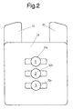
- Fig. 2 is a plan view thereof
- Fig. 3 is a bottom view thereof.
- the shoe deodorizing apparatus 10 of the present invention includes a pair of tubular leg portions 12, 12 to be inserted into the respective shoes, each of which is substantially in the shape of a rectangular parallelepiped, and a substantially semicylindrical joining portion 14 which joins the upper ends of the pair of tubular leg portions 12, 12 at a predetermined interval.
- the lower end surfaces 16 of the pair of leg portions 12, 12 are respectively formed with recesses 18, in which ultraviolet lamps 20 are respectively received.
- protrusions 22 are respectively formed at fore and hind corners in the lower end surface 16 of each leg portion 12.
- the shoe deodorizing apparatus 10 of the present invention can be self-supported by the protrusions 22 totaling four, which are formed at the fore and hind corners of the pair of leg portions 12, 12 (as best shown in Fig. 3).
- numerals 24, 24 designate batteries.
- the shoe deodorizing apparatus 10 of the present invention can be operated by a total battery voltage of 3 (V) which is produced by the two alkaline batteries of "AAA" size 24, 24.
- numeral 26 designates a buzzer for sounding the start and end of the operation of the shoe deodorizing apparatus 10.
- a sound emitting aperture 30 is formed in that bottom wall 28 of the joining portion 14 on which the buzzer 26 is put.
- numeral 32 designates an actuating switch. As shown in Fig. 2, such switches 32 in the number of three (a switch 32a with numeral 1 indicated, a switch 32b with numeral 2 indicated, and a switch 32c with numeral 3 indicated) are disposed on the upside of the joining portion 14.
- An LED (light emitting diode) 34 is built in each switch 32, and it is adapted to blink for a predetermined time in interlocking with the depressed movement of the corresponding switch 32.
- Shown at numeral 36 is a drive unit which includes a timer circuit 38 to be explained later, for controlling the lighting-up time of each ultraviolet lamp 20 and the sounding time of the buzzer 26, and an inverter circuit 40 to be explained later, for controlling the lighting-up drive of each ultraviolet lamp 20.
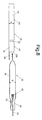
- the ultraviolet lamp 20 includes a gastight envelope 42 which is formed by bending a slender glass pipe substantially in the shape of letter U and then melting and sealing the openings of both the ends thereof, a pair of discharging electrodes 44, 44 which are respectively arranged in the vicinities of both the end sealed parts of the gastight envelope 42, and a trigger electrode 46 which is arranged around the gastight envelope 42.
- the gastight envelope 42 is made of silica glass which has the property of transmitting ultraviolet radiation at wavelengths of at least 180 (nm), and it includes a substantially U-shaped tube portion 48 and a sealing portion 50.
- the sealing portion 50 is formed by melting both the end opening parts of the tube portion 48 and thereafter squeeze-molding the molten parts, the lateral width X of this sealing portion 50 is greater than that Y of the tube portion 48.
- the tube portion 48 of the gastight envelope 42 is filled up with, for example, an ultraviolet emission gas in which argon and mercury are mixed, or an ultraviolet emission gas which consists principally of xenon, as a discharge gas for generating the ultraviolet radiation.
- Each of the discharging electrodes 44, 44 is made of a funnel-shaped member of tungsten, the distal end of which is exposed inside the tube portion 48 of the gastight envelope 42 and the base end of which is welded to a molybdenum foil 52 buried in the sealing portion 50 of the gastight envelope 42.
- One end of the corresponding one of lead terminals 54, 54 is also connected to the foil 52.
- the other end of each of the lead terminals 54, 54 is led out of the gastight envelope 42.
- the trigger electrode 46 is disposed in order to permit the low drive voltage of the ultraviolet lamp 20, and it is made of a stainless steel plate having a high reflection efficiency for the ultraviolet radiation. As shown in Figs. 5 through 7, it includes a flat portion 56, and a pair of crooked portions 58, 58 which are respectively curved substantially in the shapes of circular arcs from both the right and left side edges of the flat portion 56 inward of this flat portion 56. The distal ends of the pair of crooked portions 58, 58 are spaced so as to define an open portion 60a. Also, the upper and lower ends of the trigger electrode 46 define open portions 60b and 60c, respectively.
- Notches 62, 62 are respectively provided at the intermediate positions of the pair of crooked portions 58, 58. Referring to Fig. 5, those parts of the crooked portions 58, 58 and the flat portion 56 which lie above the notches 62, 62 constitute a tube portion holder 64 for the gastight envelope 42, and those parts of the crooked portions 58, 58 and the flat portion 56 which lie below the notches 62, 62 constitute a sealing portion holder 66 for the gastight envelope 42.
- the notches 62, 62 are respectively formed at the positions which correspond to the vicinity of the boundary between the tube portion 48 and sealing portion 50 of the gastight envelope 42 when this gastight envelope 42 is inserted into the trigger electrode 46 (as will be explained later).
- connection terminal 68 is extended from the lower end of the flat portion 56.
- the lateral width Z (Fig. 7) of the flat portion 56 is set somewhat smaller than that X of the sealing portion 50 of the gastight envelope 42, and the height h of the crooked portion 58 is set somewhat smaller than that H of the tube portion 48 of the gastight envelope 42 (as shown in Fig. 8).
- the gastight envelope 42 is inserted from the side of the open portion 60c at the lower end of the trigger electrode 46 having the above construction, as indicated by an arrow in Fig. 8, until the vicinity of the boundary between the tube portion 48 and sealing portion 50 of the gastight envelope 42 is arranged at the position corresponding to the notches 62, 62 of the crooked portions 58, 58 of the trigger electrode 46.
- the outer peripheral surface of the gastight envelope 42 is surrounded with the flat portion 56 and crooked portions 58 of the trigger electrode 46, except those parts of the gastight envelope 42 which correspond to the open portion 60a between the distal ends of the crooked portions 58, 58 and the open portions 60b, 60c at the upper and lower ends in the trigger electrode 46 (refer to Figs. 9 and 10).
- a cushion member 70 made of foamed urethane is held in close contact with the back surface of the flat portion 56 of the trigger electrode 46, namely, the surface of the flat portion 56 opposite to the surface thereof confronting the tube portion 48 (as shown in Fig. 1). As a result, the shock resistance of the ultraviolet lamp 20 is heightened.
- the height h of the crooked portion 58 of the trigger electrode 46 is set somewhat smaller than that H of the tube portion 48 of the gastight envelope 42. Therefore, the crooked portions 58, 58 of the trigger electrode 46 come into pressed contact with the tube portion 48 of the gastight envelope 42. As a result, the tube portion 48 is securely held in pressed contact by the crooked portions 58, 58 and flat portion 56 which constitute the tube portion holder 64 of the trigger electrode 46 (refer to Fig. 11).
- the lateral width Z of the flat portion 56 of the trigger electrode 46 is set somewhat smaller than that X of the sealing portion 50 of the gastight envelope 42. Therefore, the crooked portions 58, 58 of the trigger electrode 46 come into pressed contact with the sealing portion 50 of the gastight envelope 42. As a result, the sealing portion 50 is securely held in pressed contact by the crooked portions 58, 58 which constitute the sealing portion holder 66 of the trigger electrode 46 (refer to Fig. 4).
- the gastight envelope 42 of the ultraviolet lamp 20 is securely held in pressed contact by the tube portion holder 64 and sealing portion holder 66 of the trigger electrode 46, so that the mechanical strength of the gastight envelope 42 is enhanced. It is accordingly possible to thin the silica glass constructing the gastight envelope 42, with the sufficient mechanical strength ensured, and to increase the quantity of transmission of the ultraviolet radiation through the gastight envelope 42.
- the reason why the notches 62, 62 are provided in the respective crooked portions 58, 58 of the trigger electrode 46 at the positions corresponding to the vicinity of the boundary between the tube portion 48 and sealing portion 50 of the gastight envelope 42, is as follows:
- the lateral width X of the sealing portion 50 of the gastight envelope 42 is greater than that Y of the tube portion 48 thereof.
- the parts of the crooked portions 58, 58 corresponding to the tube portion holder 64 and those of the crooked portions 58, 58 corresponding to the sealing portion holder 66 fall into a separated state. Therefore, even when the parts of the crooked portions 58, 58 corresponding to the sealing portion holder 66 expand outwards along the outer periphery of the sealing portion 50 of the gastight envelope 42, the parts of the crooked portions 58, 58 corresponding to the tube portion holder 64 do not expand outwards. As a result, the parts of the crooked portions 58, 58 corresponding to the tube portion holder 64 can reliably hold the tube portion 48 of the gastight envelope 42 in pressed contact.
- connection terminal 68 of the trigger electrode 46 and the mating lead terminal 54 of one discharging electrode 44 are connected, whereupon an A. C. voltage at 50 - 60 (kHz) is applied to the pair of discharging electrodes 44, 44 and the trigger electrode 46 through the inverter circuit 40 (in Fig. 13).
- the voltage of the trigger electrode 46 becomes the same polarity as that of one discharging electrode 44 connected through the connection terminal 68 as well as the mating lead terminal 54, and the opposite polarity to that of the other discharging electrode 44.
- the distance between the trigger electrode 46 and the other discharging electrode 44 of the opposite polarity is smaller than the discharging gap between the pair of discharging electrodes 44, 44.
- the ions emitted into the tube portion 48 by the high electric-field state established between the trigger electrode 46 and the other discharging electrode 44 are attracted toward one discharging electrode 44 opposite in polarity to these ions, thereby to proceed inside the tube portion 48.
- the outer peripheral surface of the tube portion 48 is surrounded with the flat portion 56 and crooked portions 58, 58 of the trigger electrode 46, and the trigger electrode 46 opposite in polarity to the emitted ions is equivalently arranged along the discharging path across the discharging electrodes 44, 44 within the tube portion 48. Therefore, the proceeding of the ions is accelerated to contribute to the low voltage drive of the ultraviolet lamp 20.
- the shoe deodorizing apparatus 10 of the present invention employing such ultraviolet lamps 20, 20 can be operated for a long time by the two alkaline batteries of "AAA" size 24, 24.
- ultraviolet radiation at a wavelength of 185 (nm) having an ozone generating action and ultraviolet radiation at a wavelength of 254 (nm) having a sterilizing action are emitted from the ultraviolet emission gas.
- the emitted ultraviolet radiations are transmitted through those parts of the tube portion 48 which correspond to the respective open portions 60a and 60b of the trigger electrode 46 and which are not surrounded with the flat portion 56 and crooked portions 58, 58 of the trigger electrode 46.
- the ultraviolet radiation at the wavelength of 185 (nm) transmitted through the tube portion 48 acts on oxygen contained in the air, thereby to generate ozone.
- the generated ozone is emitted out of the leg portion 12 from the opening 19 of the recess 18.
- part of the ultraviolet radiation at the wavelength of 185 (nm) is emitted out of the leg portion 12 from the opening 19 of the recess 18, and it acts on the air outside the leg portion 12, thereby to generate ozone.
- the ultraviolet radiation at the wavelength of 254 (nm) transmitted through the tube portion 48 is emitted out of the leg portion 12 from the opening 19 of the recess 18.
- the trigger electrode 46 is made of the stainless steel plate which has the high reflection efficiency for the ultraviolet radiation.
- the ultraviolet radiations emitted toward the flat portion 56 and crooked portions 58, 58 of the trigger electrode 46 surrounding the tube portion 48 are reflected from the surfaces of these portions 56 and 58, 58 confronting the tube portion 48, and they are guided toward the parts of the tube portion 48 not surrounded with the flat portion 56 and crooked portions 58, 58 of the trigger electrode 46.
- a pair of shoes 72, 72 are placed astride of the joining portion 14 of the shoe deodorizing apparatus 10 of the present invention, and the leg portions 12, 12 are respectively inserted into the interiors of the right and left shoes 72, 72.
- the ultraviolet lamps 20, 20 received in the recesses 18, 18 of the leg lower-end surfaces 16, 16 and the soles 74, 74 of the shoes 72, 72 are arranged in opposition with a predetermined spacing held therebetween.
- the ultraviolet lamps 20, 20 are driven to light up for a predetermined time by the operations of the timer circuit 38 and the inverter circuit 40.
- the ultraviolet lamps 20, 20 are lit up for 1 minute in total by changing-over the ultraviolet lamp 20 of one leg portion 12 and that 20 of the other leg portion 12 every 30 seconds.
- the ultraviolet lamps 20, 20 are lit up for 2 minutes in total by changing-over the ultraviolet lamp 20 of one leg portion 12 and that 20 of the other leg portion 12 every 30 seconds
- the switch 32c bearing numeral 3 is depressed
- the ultraviolet lamps 20, 20 are lit up for 3 minutes in total by changing-over the ultraviolet lamp 20 of one leg portion 12 and that 20 of the other leg portion 12 every 30 seconds. Accordingly, the user of the shoe deodorizing apparatus 10 can select any of the three sorts of lighting-up times of the ultraviolet lamps 20, 20 in accordance with the extent of the bad smell of the shoes 72, 72.
- the consumption of the batteries 24, 24 can be relieved by alternately driving the ultraviolet lamp 20 of one leg portion 12 and that 20 of the other leg portion 12 to light up as stated above.
- the timer circuit 38 is set so as to sound the buzzer 26 for 64 (milliseconds) at the depression of the switch 32, and for 30 (seconds) at the end of the lighting-up of the ultraviolet lamps 20, 20.
- the LED 34 built in the switch 32 blinks for indication at intervals of 2 (seconds) in interlocking with the depressed movement of the switch 32.
- ozone is generated by ultraviolet radiation at a wavelength of 185 (nm) emitted from the ultraviolet lamp 20, and it is emitted out of the leg portion 12 from the opening 19 of the recess 18. Since the emitted ozone is heavier than the air, it diffuses toward the sole 74, with the result that the interior of the shoe 72 is deodorized and sterilized by the function of the ozone. Besides, part of the ultraviolet radiation at the wavelength of 185 (nm) is emitted out of the leg portion 12 from the opening 19 of the recess 18, and it acts on the air outside the leg portion 12, thereby to generate ozone, by which the interior of the shoe 72 is deodorized and sterilized.
- ultraviolet radiation at a wavelength of 254 (nm) having a sterilizing action is emitted from the ultraviolet lamp 20, and it is emitted out of the leg portion 12 from the opening 19 of the recess 18. Since the ultraviolet radiation at the wavelength of 254 (nm) is also emitted and diffused toward the sole 74, the propagation of bacilli forming the origin of the bad smell can be suppressed.
- the gap corresponding to the height of the protrusions 22 formed on the leg portion 12 is secured between the lower end surface 16 of the leg portion 12 and the sole 74 as explained before, and hence, the ozone and the ultraviolet radiation at the wavelength of 254 (nm) as are generated by the ultraviolet lamp 20 are diffused through the gap.
- a pair of shoes 72, 72 are placed astride of a joining portion 14, and leg portions 12, 12 are respectively inserted into the interiors of the right and left shoes 72, 72, whereby the interiors of the pair of shoes 72, 72 can be deodorized at one time owing to the functions of ozone and ultraviolet radiation generated by the ultraviolet lamps 20, 20 received in the leg portions 12, 12.
Abstract
Description
Claims (5)
- A deodorizing apparatus for shoes, comprising a pair of leg portions which are to be inserted into the shoes, a joining portion which joins upper ends of said pair of leg portions at a predetermined interval, ozone generating ultraviolet lamps which are respectively received in said pair of leg portions, and a power supply which drives said ultraviolet lamps to light up, wherein each of said leg portions is formed with an ozone emitting portion for emitting ozone generated by the corresponding ultraviolet lamp, and/or an ultraviolet radiation emitting portion for emitting ultraviolet radiation of a wavelength having an ozone generating action as has been generated by said corresponding ultraviolet lamp.
- A deodorizing apparatus for shoes as defined in Claim 1, wherein said ozone emitting portion and/or said ultraviolet radiation emitting portion are/is defined by an opening formed in said corresponding leg portion.
- A deodorizing apparatus for shoes as defined in Claim 2, wherein recesses are respectively formed in lower end surfaces of said leg portions, each of said recesses receiving said corresponding ultraviolet lamp therein and including said opening for emitting the ozone and/or the ultraviolet radiation of the wavelength having the ozone generating action as have/has been generated by said corresponding ultraviolet lamp.
- A deodorizing apparatus for shoes as defined in Claim 3, wherein protrusions are formed on the lower end surface of said each leg portion.
- A deodorizing apparatus for shoes as defined in any of Claims 1 through 4, wherein said each ultraviolet lamp comprises a gastight envelope which is made of an ultraviolet radiation transmitting substance, and which includes a tube portion and a sealing portion formed by sealing both end openings of said tube portion, a pair of discharging electrodes which are respectively arranged near both the end sealed parts inside said gastight envelope, an ultraviolet emission gas with which said tube portion of said gastight envelope is filled up, and a trigger electrode which is arranged around said gastight envelope; said trigger electrode includes a tube portion holder which holds said tube portion of said gastight envelope in pressed contact, and a sealing portion holder which holds said sealing portion of said gastight envelope in pressed contact; and a distance between said trigger electrode and each of said discharging electrodes is made smaller than a discharging gap between said pair of discharging electrodes.
Applications Claiming Priority (2)
| Application Number | Priority Date | Filing Date | Title |
|---|---|---|---|
| US18409100P | 2000-02-22 | 2000-02-22 | |
| US184091P | 2000-02-22 |
Publications (4)
| Publication Number | Publication Date |
|---|---|
| EP1127838A2 true EP1127838A2 (en) | 2001-08-29 |
| EP1127838A9 EP1127838A9 (en) | 2002-01-02 |
| EP1127838A3 EP1127838A3 (en) | 2003-04-02 |
| EP1127838B1 EP1127838B1 (en) | 2007-07-25 |
Family
ID=22675510
Family Applications (1)
| Application Number | Title | Priority Date | Filing Date |
|---|---|---|---|
| EP01200690A Expired - Lifetime EP1127838B1 (en) | 2000-02-22 | 2001-02-22 | Flip-chip assembly of protected micromechanical devices |
Country Status (5)
| Country | Link |
|---|---|
| US (1) | US6507082B2 (en) |
| EP (1) | EP1127838B1 (en) |
| JP (1) | JP2001308225A (en) |
| AT (1) | ATE367999T1 (en) |
| DE (1) | DE60129491T2 (en) |
Cited By (1)
| Publication number | Priority date | Publication date | Assignee | Title |
|---|---|---|---|---|
| US7763975B2 (en) | 2000-02-22 | 2010-07-27 | Texas Instruments Incorporated | Flip-chip assembly of protected micromechanical devices |
Families Citing this family (36)
| Publication number | Priority date | Publication date | Assignee | Title |
|---|---|---|---|---|
| FR2800912B1 (en) * | 1999-11-04 | 2003-07-25 | St Microelectronics Sa | OPTICAL SEMICONDUCTOR PACKAGE AND METHOD FOR MANUFACTURING SUCH A PACKAGE |
| KR100332967B1 (en) * | 2000-05-10 | 2002-04-19 | 윤종용 | Method for manufacturing digital micro-mirror device(DMD) package |
| US7498196B2 (en) * | 2001-03-30 | 2009-03-03 | Megica Corporation | Structure and manufacturing method of chip scale package |
| EP1387604A1 (en) * | 2002-07-31 | 2004-02-04 | United Test Center Inc. | Bonding pads of printed circuit board capable of holding solder balls securely |
| US7071032B2 (en) * | 2002-08-01 | 2006-07-04 | Taiwan Semiconductor Manufacturing Co., Ltd. | Material to improve image sensor yield during wafer sawing |
| US20040092029A1 (en) * | 2002-10-09 | 2004-05-13 | Jones Mark L. | Method of preparing a silicon sample for analysis |
| US7223981B1 (en) * | 2002-12-04 | 2007-05-29 | Aguila Technologies Inc. | Gamma ray detector modules |
| JP2006516761A (en) | 2003-01-24 | 2006-07-06 | モンタナ ステート ユニバーシティー−ボーズマン | Off-axis variable focus and aberration control mirror and method |
| US20070035855A1 (en) * | 2003-03-03 | 2007-02-15 | Dickensheets David L | Miniature confocal optical device, system, and method |
| US7514283B2 (en) * | 2003-03-20 | 2009-04-07 | Robert Bosch Gmbh | Method of fabricating electromechanical device having a controlled atmosphere |
| JP4505189B2 (en) * | 2003-03-24 | 2010-07-21 | 富士フイルム株式会社 | Transmission type light modulation device and mounting method thereof |
| US8912174B2 (en) * | 2003-04-16 | 2014-12-16 | Mylan Pharmaceuticals Inc. | Formulations and methods for treating rhinosinusitis |
| US7075160B2 (en) | 2003-06-04 | 2006-07-11 | Robert Bosch Gmbh | Microelectromechanical systems and devices having thin film encapsulated mechanical structures |
| US6936491B2 (en) | 2003-06-04 | 2005-08-30 | Robert Bosch Gmbh | Method of fabricating microelectromechanical systems and devices having trench isolated contacts |
| US6952041B2 (en) * | 2003-07-25 | 2005-10-04 | Robert Bosch Gmbh | Anchors for microelectromechanical systems having an SOI substrate, and method of fabricating same |
| US6903860B2 (en) * | 2003-11-01 | 2005-06-07 | Fusao Ishii | Vacuum packaged micromirror arrays and methods of manufacturing the same |
| US7626255B2 (en) * | 2003-10-15 | 2009-12-01 | Koninklijke Philips Electronics N.V. | Device, system and electric element |
| US7115436B2 (en) * | 2004-02-12 | 2006-10-03 | Robert Bosch Gmbh | Integrated getter area for wafer level encapsulated microelectromechanical systems |
| US7068125B2 (en) * | 2004-03-04 | 2006-06-27 | Robert Bosch Gmbh | Temperature controlled MEMS resonator and method for controlling resonator frequency |
| US7102467B2 (en) * | 2004-04-28 | 2006-09-05 | Robert Bosch Gmbh | Method for adjusting the frequency of a MEMS resonator |
| KR100789545B1 (en) | 2005-03-07 | 2007-12-28 | 삼성전기주식회사 | Optical modulator module package using flip-chip mounting technology |
| KR100815350B1 (en) | 2005-04-01 | 2008-03-19 | 삼성전기주식회사 | Packaging structure for optical modulator |
| US7449355B2 (en) * | 2005-04-27 | 2008-11-11 | Robert Bosch Gmbh | Anti-stiction technique for electromechanical systems and electromechanical device employing same |
| US7529013B2 (en) * | 2005-08-29 | 2009-05-05 | Samsung Electro-Mechanics Co., Ltd. | Optical modulator module package |
| KR100861063B1 (en) | 2005-08-29 | 2008-09-30 | 삼성전기주식회사 | Optical modulator module package |
| JP2007095780A (en) * | 2005-09-27 | 2007-04-12 | Oki Electric Ind Co Ltd | Tool and method for manufacturing semiconductor device |
| KR100836658B1 (en) | 2005-10-11 | 2008-06-10 | 삼성전기주식회사 | Optical modulator module package and Manufacturing Method thereof |
| KR100857172B1 (en) | 2005-10-11 | 2008-09-05 | 삼성전기주식회사 | Mems module package |
| US20070170528A1 (en) | 2006-01-20 | 2007-07-26 | Aaron Partridge | Wafer encapsulated microelectromechanical structure and method of manufacturing same |
| JP2007264441A (en) * | 2006-03-29 | 2007-10-11 | Fujitsu Ltd | Optical coupling method |
| US7456042B2 (en) * | 2006-06-04 | 2008-11-25 | Robert Bosch Gmbh | Microelectromechanical systems having stored charge and methods for fabricating and using same |
| US7824943B2 (en) * | 2006-06-04 | 2010-11-02 | Akustica, Inc. | Methods for trapping charge in a microelectromechanical system and microelectromechanical system employing same |
| JP5349024B2 (en) * | 2007-11-29 | 2013-11-20 | 京セラ株式会社 | Optical device and method of manufacturing optical device |
| US7875482B2 (en) | 2009-03-19 | 2011-01-25 | Robert Bosch Gmbh | Substrate with multiple encapsulated pressures |
| US8430255B2 (en) * | 2009-03-19 | 2013-04-30 | Robert Bosch Gmbh | Method of accurately spacing Z-axis electrode |
| JP5133956B2 (en) * | 2009-09-25 | 2013-01-30 | 大日本スクリーン製造株式会社 | Spatial light modulator and exposure apparatus |
Citations (5)
| Publication number | Priority date | Publication date | Assignee | Title |
|---|---|---|---|---|
| EP0675536A1 (en) * | 1994-03-31 | 1995-10-04 | AT&T Corp. | Process for fabricating an integrated circuit |
| WO1998005935A1 (en) * | 1996-08-08 | 1998-02-12 | Integrated Sensing Systems, Inc. | Method for packaging microsensors |
| WO1998027411A1 (en) * | 1996-12-17 | 1998-06-25 | Laboratorium Für Physikalische Elektronik Institut Für Quantenelektronik | Method for applying a microsystem or a converter on a substrate, and device manufactured accordingly |
| US5936758A (en) * | 1996-04-12 | 1999-08-10 | Texas Instruments Incorporated | Method of passivating a micromechanical device within a hermetic package |
| EP0977253A2 (en) * | 1998-05-06 | 2000-02-02 | Texas Instruments Incorporated | Flip-chip bonding of semiconductor chips |
Family Cites Families (3)
| Publication number | Priority date | Publication date | Assignee | Title |
|---|---|---|---|---|
| JPH02278872A (en) * | 1989-04-20 | 1990-11-15 | Ibiden Co Ltd | Image sensor |
| US5293511A (en) * | 1993-03-16 | 1994-03-08 | Texas Instruments Incorporated | Package for a semiconductor device |
| US5610431A (en) * | 1995-05-12 | 1997-03-11 | The Charles Stark Draper Laboratory, Inc. | Covers for micromechanical sensors and other semiconductor devices |
-
2001
- 2001-02-08 US US09/779,001 patent/US6507082B2/en not_active Expired - Lifetime
- 2001-02-22 EP EP01200690A patent/EP1127838B1/en not_active Expired - Lifetime
- 2001-02-22 JP JP2001046620A patent/JP2001308225A/en not_active Abandoned
- 2001-02-22 AT AT01200690T patent/ATE367999T1/en not_active IP Right Cessation
- 2001-02-22 DE DE60129491T patent/DE60129491T2/en not_active Expired - Lifetime
Patent Citations (5)
| Publication number | Priority date | Publication date | Assignee | Title |
|---|---|---|---|---|
| EP0675536A1 (en) * | 1994-03-31 | 1995-10-04 | AT&T Corp. | Process for fabricating an integrated circuit |
| US5936758A (en) * | 1996-04-12 | 1999-08-10 | Texas Instruments Incorporated | Method of passivating a micromechanical device within a hermetic package |
| WO1998005935A1 (en) * | 1996-08-08 | 1998-02-12 | Integrated Sensing Systems, Inc. | Method for packaging microsensors |
| WO1998027411A1 (en) * | 1996-12-17 | 1998-06-25 | Laboratorium Für Physikalische Elektronik Institut Für Quantenelektronik | Method for applying a microsystem or a converter on a substrate, and device manufactured accordingly |
| EP0977253A2 (en) * | 1998-05-06 | 2000-02-02 | Texas Instruments Incorporated | Flip-chip bonding of semiconductor chips |
Non-Patent Citations (1)
| Title |
|---|
| PATENT ABSTRACTS OF JAPAN vol. 015, no. 046 (E-1029), 4 February 1991 (1991-02-04) -& JP 02 278872 A (IBIDEN CO LTD), 15 November 1990 (1990-11-15) * |
Cited By (1)
| Publication number | Priority date | Publication date | Assignee | Title |
|---|---|---|---|---|
| US7763975B2 (en) | 2000-02-22 | 2010-07-27 | Texas Instruments Incorporated | Flip-chip assembly of protected micromechanical devices |
Also Published As
| Publication number | Publication date |
|---|---|
| DE60129491T2 (en) | 2008-04-17 |
| EP1127838B1 (en) | 2007-07-25 |
| EP1127838A9 (en) | 2002-01-02 |
| US6507082B2 (en) | 2003-01-14 |
| US20020163055A1 (en) | 2002-11-07 |
| EP1127838A3 (en) | 2003-04-02 |
| ATE367999T1 (en) | 2007-08-15 |
| JP2001308225A (en) | 2001-11-02 |
| DE60129491D1 (en) | 2007-09-06 |
Similar Documents
| Publication | Publication Date | Title |
|---|---|---|
| EP1127838A2 (en) | Flip-chip assembly of protected micromechanical devices | |
| EP1121874A2 (en) | Deodorizing apparatus for shoes | |
| JP4240437B2 (en) | Gas discharge tube | |
| WO2007078786A3 (en) | Ceramic metal halide lamp | |
| ES2025500A6 (en) | Low watt metal halide lamp. | |
| EP0083874B1 (en) | Beam mode fluorescent lamp | |
| CN110234581B (en) | Portable water cup | |
| EP1257154A3 (en) | Light source device | |
| KR100827914B1 (en) | Gas discharge tube | |
| KR102301283B1 (en) | UV sterilization device for elevator | |
| WO2005013441A3 (en) | Cathodes for fluorine gas discharge lasers | |
| WO2000034983A1 (en) | Gas discharge tube | |
| EP1308987A3 (en) | Super-high pressure discharge lamp of the short arc type | |
| EP1641023A3 (en) | Ignition aid for high intensity discharge lamp | |
| CN111839764A (en) | Tooth orthodontic auxiliary device | |
| KR100822082B1 (en) | Deodorization apparatus supplied electric power by electromagnetic induction,and a toilet cover | |
| US4361782A (en) | Jacketed discharge lamp having oxidizable fail-safe switch | |
| EP1351277A3 (en) | Metal halide filling composition and corresponding lamp | |
| JP3437835B2 (en) | UV lamp | |
| WO2000034982A1 (en) | Gas discharge tube | |
| JP4237400B2 (en) | Gas discharge tube | |
| EP1538655A3 (en) | Ion implantation ion source | |
| JP3409008B2 (en) | UV lamp | |
| WO2008112102A3 (en) | Starting aid for low wattage metal halide lamps | |
| JP2007098014A (en) | Ozone deodorization and sterilization apparatus |
Legal Events
| Date | Code | Title | Description |
|---|---|---|---|
| PUAI | Public reference made under article 153(3) epc to a published international application that has entered the european phase |
Free format text: ORIGINAL CODE: 0009012 |
|
| 17P | Request for examination filed |
Effective date: 20010222 |
|
| AK | Designated contracting states |
Kind code of ref document: A2 Designated state(s): AT BE CH CY DE DK ES FI FR GB GR IE IT LI LU MC NL PT SE TR |
|
| AX | Request for extension of the european patent |
Free format text: AL;LT;LV;MK;RO;SI |
|
| PUAL | Search report despatched |
Free format text: ORIGINAL CODE: 0009013 |
|
| AK | Designated contracting states |
Designated state(s): AT BE CH CY DE DK ES FI FR GB GR IE IT LI LU MC NL PT SE TR Kind code of ref document: A3 Designated state(s): AT BE CH CY DE DK ES FI FR GB GR IE IT LI LU MC NL PT SE TR |
|
| AX | Request for extension of the european patent |
Extension state: AL LT LV MK RO SI |
|
| AKX | Designation fees paid |
Designated state(s): DE FR GB |
|
| 17Q | First examination report despatched |
Effective date: 20040127 |
|
| GRAP | Despatch of communication of intention to grant a patent |
Free format text: ORIGINAL CODE: EPIDOSNIGR1 |
|
| RBV | Designated contracting states (corrected) |
Designated state(s): AT BE CH CY DE DK ES FI FR GB GR IE IT LI LU MC NL PT SE TR |
|
| GRAS | Grant fee paid |
Free format text: ORIGINAL CODE: EPIDOSNIGR3 |
|
| GRAA | (expected) grant |
Free format text: ORIGINAL CODE: 0009210 |
|
| AK | Designated contracting states |
Kind code of ref document: B1 Designated state(s): AT BE CH CY DE DK ES FI FR GB GR IE IT LI LU MC NL PT SE TR |
|
| REG | Reference to a national code |
Ref country code: GB Ref legal event code: FG4D |
|
| REG | Reference to a national code |
Ref country code: CH Ref legal event code: EP |
|
| REG | Reference to a national code |
Ref country code: IE Ref legal event code: FG4D |
|
| REF | Corresponds to: |
Ref document number: 60129491 Country of ref document: DE Date of ref document: 20070906 Kind code of ref document: P |
|
| ET | Fr: translation filed | ||
| PG25 | Lapsed in a contracting state [announced via postgrant information from national office to epo] |
Ref country code: NL Free format text: LAPSE BECAUSE OF FAILURE TO SUBMIT A TRANSLATION OF THE DESCRIPTION OR TO PAY THE FEE WITHIN THE PRESCRIBED TIME-LIMIT Effective date: 20070725 Ref country code: FI Free format text: LAPSE BECAUSE OF FAILURE TO SUBMIT A TRANSLATION OF THE DESCRIPTION OR TO PAY THE FEE WITHIN THE PRESCRIBED TIME-LIMIT Effective date: 20070725 Ref country code: ES Free format text: LAPSE BECAUSE OF FAILURE TO SUBMIT A TRANSLATION OF THE DESCRIPTION OR TO PAY THE FEE WITHIN THE PRESCRIBED TIME-LIMIT Effective date: 20071105 Ref country code: PT Free format text: LAPSE BECAUSE OF FAILURE TO SUBMIT A TRANSLATION OF THE DESCRIPTION OR TO PAY THE FEE WITHIN THE PRESCRIBED TIME-LIMIT Effective date: 20071226 |
|
| REG | Reference to a national code |
Ref country code: CH Ref legal event code: PL |
|
| NLV1 | Nl: lapsed or annulled due to failure to fulfill the requirements of art. 29p and 29m of the patents act | ||
| PG25 | Lapsed in a contracting state [announced via postgrant information from national office to epo] |
Ref country code: LI Free format text: LAPSE BECAUSE OF FAILURE TO SUBMIT A TRANSLATION OF THE DESCRIPTION OR TO PAY THE FEE WITHIN THE PRESCRIBED TIME-LIMIT Effective date: 20070725 Ref country code: AT Free format text: LAPSE BECAUSE OF FAILURE TO SUBMIT A TRANSLATION OF THE DESCRIPTION OR TO PAY THE FEE WITHIN THE PRESCRIBED TIME-LIMIT Effective date: 20070725 Ref country code: CH Free format text: LAPSE BECAUSE OF FAILURE TO SUBMIT A TRANSLATION OF THE DESCRIPTION OR TO PAY THE FEE WITHIN THE PRESCRIBED TIME-LIMIT Effective date: 20070725 |
|
| PG25 | Lapsed in a contracting state [announced via postgrant information from national office to epo] |
Ref country code: BE Free format text: LAPSE BECAUSE OF FAILURE TO SUBMIT A TRANSLATION OF THE DESCRIPTION OR TO PAY THE FEE WITHIN THE PRESCRIBED TIME-LIMIT Effective date: 20070725 |
|
| PG25 | Lapsed in a contracting state [announced via postgrant information from national office to epo] |
Ref country code: GR Free format text: LAPSE BECAUSE OF FAILURE TO SUBMIT A TRANSLATION OF THE DESCRIPTION OR TO PAY THE FEE WITHIN THE PRESCRIBED TIME-LIMIT Effective date: 20071026 |
|
| PLBE | No opposition filed within time limit |
Free format text: ORIGINAL CODE: 0009261 |
|
| STAA | Information on the status of an ep patent application or granted ep patent |
Free format text: STATUS: NO OPPOSITION FILED WITHIN TIME LIMIT |
|
| PG25 | Lapsed in a contracting state [announced via postgrant information from national office to epo] |
Ref country code: SE Free format text: LAPSE BECAUSE OF FAILURE TO SUBMIT A TRANSLATION OF THE DESCRIPTION OR TO PAY THE FEE WITHIN THE PRESCRIBED TIME-LIMIT Effective date: 20071025 |
|
| 26N | No opposition filed |
Effective date: 20080428 |
|
| PG25 | Lapsed in a contracting state [announced via postgrant information from national office to epo] |
Ref country code: MC Free format text: LAPSE BECAUSE OF NON-PAYMENT OF DUE FEES Effective date: 20080228 |
|
| PG25 | Lapsed in a contracting state [announced via postgrant information from national office to epo] |
Ref country code: IE Free format text: LAPSE BECAUSE OF NON-PAYMENT OF DUE FEES Effective date: 20080222 |
|
| PG25 | Lapsed in a contracting state [announced via postgrant information from national office to epo] |
Ref country code: CY Free format text: LAPSE BECAUSE OF FAILURE TO SUBMIT A TRANSLATION OF THE DESCRIPTION OR TO PAY THE FEE WITHIN THE PRESCRIBED TIME-LIMIT Effective date: 20070725 |
|
| PG25 | Lapsed in a contracting state [announced via postgrant information from national office to epo] |
Ref country code: DK Free format text: LAPSE BECAUSE OF FAILURE TO SUBMIT A TRANSLATION OF THE DESCRIPTION OR TO PAY THE FEE WITHIN THE PRESCRIBED TIME-LIMIT Effective date: 20070725 |
|
| PG25 | Lapsed in a contracting state [announced via postgrant information from national office to epo] |
Ref country code: LU Free format text: LAPSE BECAUSE OF NON-PAYMENT OF DUE FEES Effective date: 20080222 |
|
| PG25 | Lapsed in a contracting state [announced via postgrant information from national office to epo] |
Ref country code: TR Free format text: LAPSE BECAUSE OF FAILURE TO SUBMIT A TRANSLATION OF THE DESCRIPTION OR TO PAY THE FEE WITHIN THE PRESCRIBED TIME-LIMIT Effective date: 20070725 |
|
| PG25 | Lapsed in a contracting state [announced via postgrant information from national office to epo] |
Ref country code: IT Free format text: LAPSE BECAUSE OF NON-PAYMENT OF DUE FEES Effective date: 20080229 |
|
| REG | Reference to a national code |
Ref country code: FR Ref legal event code: PLFP Year of fee payment: 16 |
|
| PGFP | Annual fee paid to national office [announced via postgrant information from national office to epo] |
Ref country code: DE Payment date: 20160302 Year of fee payment: 16 |
|
| PGFP | Annual fee paid to national office [announced via postgrant information from national office to epo] |
Ref country code: FR Payment date: 20160125 Year of fee payment: 16 Ref country code: GB Payment date: 20160127 Year of fee payment: 16 |
|
| REG | Reference to a national code |
Ref country code: DE Ref legal event code: R119 Ref document number: 60129491 Country of ref document: DE |
|
| GBPC | Gb: european patent ceased through non-payment of renewal fee |
Effective date: 20170222 |
|
| REG | Reference to a national code |
Ref country code: FR Ref legal event code: ST Effective date: 20171031 |
|
| PG25 | Lapsed in a contracting state [announced via postgrant information from national office to epo] |
Ref country code: FR Free format text: LAPSE BECAUSE OF NON-PAYMENT OF DUE FEES Effective date: 20170228 Ref country code: DE Free format text: LAPSE BECAUSE OF NON-PAYMENT OF DUE FEES Effective date: 20170901 |
|
| PG25 | Lapsed in a contracting state [announced via postgrant information from national office to epo] |
Ref country code: GB Free format text: LAPSE BECAUSE OF NON-PAYMENT OF DUE FEES Effective date: 20170222 |