EP1111791A1 - Logic circuit and full adder using the same - Google Patents
Logic circuit and full adder using the same Download PDFInfo
- Publication number
- EP1111791A1 EP1111791A1 EP00403396A EP00403396A EP1111791A1 EP 1111791 A1 EP1111791 A1 EP 1111791A1 EP 00403396 A EP00403396 A EP 00403396A EP 00403396 A EP00403396 A EP 00403396A EP 1111791 A1 EP1111791 A1 EP 1111791A1
- Authority
- EP
- European Patent Office
- Prior art keywords
- signal
- level
- logic
- output
- exclusive
- Prior art date
- Legal status (The legal status is an assumption and is not a legal conclusion. Google has not performed a legal analysis and makes no representation as to the accuracy of the status listed.)
- Withdrawn
Links
Images


Classifications
-
- G—PHYSICS
- G06—COMPUTING; CALCULATING OR COUNTING
- G06F—ELECTRIC DIGITAL DATA PROCESSING
- G06F7/00—Methods or arrangements for processing data by operating upon the order or content of the data handled
- G06F7/38—Methods or arrangements for performing computations using exclusively denominational number representation, e.g. using binary, ternary, decimal representation
- G06F7/48—Methods or arrangements for performing computations using exclusively denominational number representation, e.g. using binary, ternary, decimal representation using non-contact-making devices, e.g. tube, solid state device; using unspecified devices
- G06F7/50—Adding; Subtracting
- G06F7/501—Half or full adders, i.e. basic adder cells for one denomination
-
- H—ELECTRICITY
- H03—ELECTRONIC CIRCUITRY
- H03K—PULSE TECHNIQUE
- H03K19/00—Logic circuits, i.e. having at least two inputs acting on one output; Inverting circuits
- H03K19/20—Logic circuits, i.e. having at least two inputs acting on one output; Inverting circuits characterised by logic function, e.g. AND, OR, NOR, NOT circuits
- H03K19/21—EXCLUSIVE-OR circuits, i.e. giving output if input signal exists at only one input; COINCIDENCE circuits, i.e. giving output only if all input signals are identical
- H03K19/215—EXCLUSIVE-OR circuits, i.e. giving output if input signal exists at only one input; COINCIDENCE circuits, i.e. giving output only if all input signals are identical using field-effect transistors
Definitions
- circuit shown in Fig. 1 has been generally frequently used as an EXOR logic circuit
- circuit shown in Fig. 2 has been generally frequently used as an EXNOR logic circuit (refer to for example John P. Uyemura, "CMOS LOGIC CIRCUIT DESIGN", Kluwer Academic Publishers, 1999, pp. 274 to pp. 275, Fig. 6.21 to 6.22).
- An EXOR logic circuit 1 of Fig. 1 comprises two CMOS transmission gates TMG11 and TMG12 and two CMOS inverters INVI and INV12 and is configured by eight transistors in total.
- an input terminal TIN11 of a logic signal A is connected to an input terminal of an inverter INV11, a gate of a p-channel MOS (PMOS) transistor of the transmission gate TMG11, and a gate of an n-channel MOS (NMOS) transistor of the transmission gate TMG12.
- PMOS p-channel MOS
- NMOS n-channel MOS
- An output terminal of the inverter INV11 is connected to a gate of the NMOS transistor of the transmission gate TMG11 and a gate of the PMOS transistor of the transmission gate Tb4G12.
- an input terminal TIN12 of a logic signal B is connected to an input terminal of the inverter INV12 and one input/output terminal of the transmission gate TMG11, while an output terminal of the inverter INV12 is connected to one input/output terminal of the transmission gate TMG12.
- the other input/output terminals of the transmission gates TMG11 and TMG12 are commonly connected to an output terminal TOT11 of an exclusive-OR A(+)B.
- an EXNOR logic circuit 2 of Fig. 2 comprises two CMOS transmission gates TMG21 and TMG22 and two CMOS inverters INV21 and INV22 and is configured by eight transistors in total.
- an input terminal TIN21 of the logic signal A is connected to the input terminal of an inverter INV21, a gate of the PMOS transistor of the transmission gate TMG21, and a gate of the NMOS transistor of the transmission gate TMG22.
- An output terminal of the inverter INV21 is connected to a gate of the NMOS transistor of the transmission gate TMG2I and a gate of the PMOS transistor of the transmission gate TMG22.
- an input terminal TIN22 of the logic signal B is connected to an input terminal of the inverter INV22 and one input/output terminal of the transmission gate TMG22, while an output terminal of the inverter INV22 is connected to one input/output terminal of the transmission gate TMG21.
- the other input/output terminals of the transmission gates TMG21 and TMG22 are commonly connected to an output terminal TOT21 of a dual signal A ⁇ (+)B of the exclusive-OR A(+)B.
- the 6tr type EXOR circuit 3 shown in Fig. 3 comprises a PMOS transistor PT31, an NMOS transistor NT31, a transmission gate TMG31, and an inverter lNV31 and is configured by six transistors in total.
- An input terminal TIN3 of the logic signal A is connected to the gates of the PMOS transistor PT31 and the NMOS transistor NT31 and one input/output terminal of the transmission gate TMG31.
- An input terminal TIN32 of the logic signal B is connected to a source of the PMOS transistor PT31 and an input terminal of the inverter INV31, while an output terminal of the inverter INV31 is connected to a source of the NMOS transistor NT31.
- the drains of the PMOS transistor PT31 and the NMOS transistor NT31 and the other input/output terminal of the transmission gate TMG31 are commonly connected to an output terminal TOT31 of the exclusive-OR A(+)B.
- the 6tr type EXNOR circuit 4 shown in Fig. 4 comprises a PMOS transistor PT41, an NMOS transistor NT41, a transmission gate TMG41, and an inverter INV41 and is configured by six transistors in total.
- An input terminal TIN41 of the logic signal A is connected to the gates of the PMOS transistor PT41 and the NMOS transistor NT41 and one input/output terminal of the transmission gate TMG41.
- An input terminal TIN42 of the logic signal B is connected to a source of the NMOS transistor NT41 and an input terminal of the inverter INV41, while an output terminal of the inverter INV41 is connected to a source of the PMOS transistor PT41.
- the drains of the PMOS transistor PT41 and the NMOS transistor NT41 and the other input/output terminal of the transmission gate TMG41 are commonly connected to an output terminal TOT41 of the dual signal A ⁇ (+)B of the exclusive-OR A(+)B.
- the 4tr type EXOR circuit 5 shown in Fig. 5 comprises PMOS transistors PT51 and PT52 and NMOS transistors NT51 and NT52 and is configured by four transistors in total.
- the PMOS transistor PT51 is connected between an input terminal TIN51 of the logic signal A and an output terminal TOT51 of the exclusive-OR A(+)B, while the PMOS transistor PT52 is connected between an input terminal TIN52 of the logic signal B and the output terminal TOT51.
- NMOS transistors NT51 and NT52 are connected in series between the output terminal TOT51 and a ground GND.
- the gate of the PMOS transistor PT52 and the gate of the NMOS transistor NT51 are connected to the input terminal TIN51, while the gate of the PMOS transistor PT51 and the gate of the NMOS transistor NT52 are connected to the input terminal TIN52.
- the 4tr type EXNOR circuit 6 shown in Fig. 6 comprises PMOS transistors PT61 and PT62 and NMOS transistors NT61 and NT62 and is configured by four transistors in total.
- the NMOS transistor NT61 is connected between an input terminal TIN61 of the logic signal A and an output terminal TOT61 of the dual signal A ⁇ (+)B of the exclusive-OR A(+)B, while the NMOS transistor NT62 is connected between an input terminal TIN62 of the logic signal B and the output terminal TOT61.
- the PMOS transistors PT61 and PT62 are connected in series between a supply line of a power supply voltage V DD and the output terminal TOT61.
- the gate of the PMOS transistor PT62 and the gate of the NMOS transistor NT62 are connected to the input terminal TIN61, while the gate of the PMOS transistor PT61 and the gate of the NMOS transistor NT61 are connected to the input terminal TIN62.
- Figure 7 is a circuit diagram of an example of the configuration of a generation circuit of a carry signal CO of a full adder.
- This carry signal generation circuit 7 is configured by an EXOR logic circuit 71, transmission gates TMG71 and TMG72, and an inverter INV71.
- An input terminal TIN71 of the logic signal A is connected to one input terminal of the EXOR logic circuit 71 and one input/output terminal of the transmission gate TMG71, while an input terminal TIN72 of the logic signal B is connected to the other input terminal of the EXOR logic circuit 71. Further, an input terminal TIN73 of the carry signal C is connected to one input/output terminal of a transmission gate TMG72.
- an output terminal of the EXOR logic circuit 71 is connected to an input terminal of the inverter INV71, a gate of the PMOS transistor of the transmission gate TMG71, and a gate of the NMOS transistor of the transmission gate TMG72.
- An output terminal of the inverter INV71 is connected to a gate of the NMOS transistor of the transmission gate TMG71 and a gate of the PMOS transistor of the transmission gate TMG72.
- the other input/output terminals of the transmission gates TMG71 and TMG72 are commonly connected to the output terminal TOT71 of the carry signal CO.
- CO AB+BC+CA
- the A ⁇ (+)B necessary for the generation of the carry signal CO is obtained by inversion of the exclusive-OR A(+)B. At this time, due to the delay of one inverter, a phase difference occurs between the signals A(+)B and A ⁇ (+)B.
- Figure 9 and Fig. 10 are diagrams of the results of simulation in the cases of conventional 8tr type and 6tr type EXOR logic circuits having inverters for inverting the input signals and passing the outputs thereof through one inverter.
- phase differences arise between the two outputs and therefore the intersecting points are not at the center values of the amplitudes.
- the PMOS transistors PT51 and PT52 cannot completely transfer the logic potential "0" and therefore a potential which has become higher by the amount of the threshold value of the PMOS transistors appears at the output.
- the NMOS transistors NT61 and NT62 cannot completely transfer the logic potential "1" and therefore a potential which has become lower by the amount of the threshold value of the NMOS transistors appears at the output.
- the present invention was made in consideration with such a circumstance and has as an object thereof to provide a logic circuit capable of suppressing an occurrence of wraparound of a signal, capable of reducing the power consumption, and achieving a reduction of circuit scale and an improvement of operating speed and a full adder using the same.
- a logic circuit comprising an exclusive-OR generation circuit for receiving a first logic signal and a second logic signal taking a first or second level and generating an exclusive-OR of the first logic signal and second logic signal, a dual signal generation circuit for receiving the first logic signal and the second logic signal taking the first or second level and generating a dual signal of the exclusive-OR of the first logic signal and second logic signal, and an interpolation circuit for compulsorily setting an output level of said dual signal at the first level when the output level of said exclusive-OR is the second level.
- a logic circuit comprising an exclusive-OR generation circuit for receiving a first logic signal and a second logic signal taking a first or second level and generating an exclusive-OR of the first logic signal and second logic signal, a dual signal generation circuit for receiving the first logic signal and the second logic signal taking the first or second level and generating a dual signal of the exclusive-OR of the first logic signal and second logic signal, and an interpolation circuit for compulsorily setting the output level of said exclusive-OR at the second level when the output level of said dual signal is the first level.
- a logic circuit comprising an exclusive-OR generation circuit for receiving a first logic signal and a second logic signal taking a first or second level and generating an exclusive-OR of the first logic signal and second logic signal, a dual signal generation circuit for receiving the first logic signal and the second logic signal taking the first or second level and generating a dual signal of the exclusive-OR of the first logic signal and second logic signal, and an interpolation circuit for compulsorily setting an output level of said dual signal at the first level when the output level of said exclusive-OR is the second level, while compulsorily setting the output level of said exclusive-OR at the second level when the output level of said dual signal is the first level.
- a logic circuit comprising a first input terminal with a first logic signal taking a first or second level input thereto; a second input terminal with a second logic signal taking a first or second level input thereto; a first output terminal for outputting an exclusive-OR; a second output terminal for outputting a dual signal of said exclusive-OR; a dual signal generation circuit having first conductivity type first and second transistors connected in series between said first level use power supply potential and said second output terminal, turning ON when the signal of second level is supplied to the control terminal, while cutting off when the signal of first level is supplied, a second conductivity type first transistor connected between said first input terminal and said second output terminal, turning ON when the signal of first level is supplied to the control terminal, while cutting off when the signal of second level is supplied, and a second conductivity type second transistor connected between said second input terminal and said second output terminal, turning on when the signal of first level is supplied to the control terminal, while cutting off when the signal of second level is supplied; an exclusive-OR
- a full adder comprising a logic circuit having an exclusive-OR generation circuit for receiving a first logic signal and a second logic signal taking a first or second level and generating an exclusive-OR of the first logic signal and second logic signal, a dual signal generation circuit for receiving the first logic signal and the second logic signal taking the first or second level and generating a dual signal of the exclusive-OR of the first logic signal and second logic signal, and an interpolation circuit for compulsorily setting an output level of said dual signal at the first level when the output level of said exclusive-OR is the second level, a sum signal generation circuit for generating a sum signal based on an exclusive-OR output and a dual signal output of said logic circuit, and a carry signal generation circuit for generating a carry signal by selecting said first logic signal or carry signal based on the exclusive-OR output and the dual signal output of said logic circuit.
- a full adder comprising a logic circuit having an exclusive-OR generation circuit for receiving a first logic signal and a second logic signal taking a first or second level and generating an exclusive-OR of the first logic signal and second logic signal, a dual signal generation circuit for receiving the first logic signal and the second logic signal taking the first or second level and generating a dual signal of the exclusive-OR of the first logic signal and second logic signal, and an interpolation circuit for compulsorily setting the output level of said exclusive-OR at the second level when the output level of said dual signal is the first level; a sum signal generation circuit for generating a sum signal based on then exclusive-OR output and the dual signal output of said logic circuit; and a carry signal generation circuit for generating a carry signal by selecting said first logic signal or carry signal based on the exclusive-OR output and the dual signal output of said logic circuit.
- a full adder comprising a logic circuit having an exclusive-OR generation circuit for receiving a first logic signal and a second logic signal taking a first or second level and generating an exclusive-OR of the first logic signal and second logic signal, a dual signal generation circuit for receiving the first logic signal and the second logic signal taking the first or second level and generating a dual signal of the exclusive-OR of the first logic signal and second logic signal, and an interpolation circuit for compulsorily setting an output level of said dual signal at the first level when the output level of said exclusive-OR is the second level, while compulsorily setting the output level of said exclusive-OR at the second level when the output level of said dual signal is the first level; a sum signal generation circuit for generating a sum signal based on an exclusive-OR output and a dual signal output of said logic circuit; and a carry signal generation circuit for generating a carry signal by selecting said first logic signal or carry signal based on the exclusive-OR output and the dual signal output of said
- a full adder comprising a logic circuit having a first input terminal with a first logic signal taking a first or second level input thereto, a second input terminal with a second logic signal taking a first or second level input thereto, a first output terminal for outputting an exclusive-OR, a second output terminal for outputting a dual signal of said exclusive-OR, a dual signal generation circuit which has first conductivity type first and second transistors connected in series between said first level use power supply potential and said second output terminal, turning ON when the signal of second level is supplied to the control terminal, while cutting off when the signal of first level is supplied, a second conductivity type first transistor connected between said first input terminal and said second output terminal, turning ON when the signal of first level is supplied to the control terminal, while cutting off when the signal of second level is supplied, and a second conductivity type second transistor connected between said second input terminal and said second output terminal, turning on when the signal of first level is supplied to the control terminal, while cutting off when the signal of second level is supplied, and a second conductivity type second transistor connected between
- control terminals of said first conductivity type second and fourth transistors and second conductivity type second and third transistors are connected to said first input terminal, the control terminals of said first conductivity type first and third transistors and second conductivity type first and fourth transistors are connected to said second input terminal, the control terminal of said first conductivity type fifth transistor is connected to said first output terminal, and the control terminal of said second conductivity type fifth transistor is connected to said second output terminal; a sum signal generation circuit for generating a sum signal based on an exclusive-OR output and a dual signal output of said logic circuit; and a carry signal generation circuit for generating a carry signal by selecting said first logic signal or carry signal based on the exclusive-OR output and the dual signal output of said logic circuit.
- said first conductivity type first, second, third, fourth, and fifth transistors are p-channel field effect transistors
- said second conductivity type first, second, third, fourth, and fifth transistors are n-channel field effect transistors.
- the output level of the exclusive-OR when the output level of the exclusive-OR is the second level, the output level of the dual signal is compulsorily set at the first level by the interpolation circuit.
- the output level of the dual signal is the first level
- the output level of the exclusive-OR is compulsorily set at the second level.
- the dual signal is generated in the logic circuit and supplied to the carry signal generation circuit.
- an inverter for inverting the logic as in the conventional circuit is unnecessary. As a result, the occurrence of wraparound of the signal is suppressed.
- Figure 13 is a circuit diagram of an embodiment of an EXOR/EXNOR logic circuit according to the present invention.
- This EXOR/EXNOR logic circuit 10 comprises PMOS transistors PT101 to PT105 as first conductivity type (p-channel) first to fifth transistors, NMOS transistors NT101 to NT105 as second conductivity type (n-channel) first to fifth transistors, a first input terminal TIN101 for the first logic signal A, a second input terminal TIN102 for the second logic signal B, a first output terminal TOT101 for the exclusive-OR A(+)B, and a second output terminal TOT102 for the dual signal A ⁇ (+)B of the exclusive-OR A(+)B.
- a dual signal generation circuit 11 is configured by the PMOS transistors PT101 and PT102 and the NMOS transistors NT101 and NT102
- an exclusive-OR circuit 12 is configured by the PMOS transistors PT103 and PT104 and the NMOS transistors NT103 and NT104
- an interpolation circuit 13 is configured by the PMOS transistor PT105 and the NMOS transistor NT105.
- the EXOR/EXNOR logic circuit 10 uses 10 transistors of the PMOS transistors PT101 to PT105 and the NMOS transistors NT101 to NT105 as the main configuration elements. There is no inverter for inverting the input signal as seen in the conventional 8tr and 6tr type logic circuits.
- the PMOS transistor PT103 is connected between the input terminal TIN101 of the logic signal A and the output terminal TOT101 of the exclusive-OR A(+)B, and the PMOS transistor PT104 is connected between the input terminal TIN 102 of the logic signal B and the output terminal TOT101.
- the NMOS transistor NT101 is connected between the input terminal TIN101 of the logic signal A and the output terminal TOT102 of the dual signal A ⁇ (+)B of the exclusive-OR A(+)B, and the NMOS transistor NT102 is connected between the input terminal TIN102 of the logic signal B and the output terminal TOT102.
- the PMOS transistors PT101 and PT102 are connected in series between the supply line of the power supply voltage VDD and the output terminal TOT102, and the PMOS transistor PT105 is connected between the supply line of the power supply voltage V DD and the output terminal TOT102 in parallel to this.
- NMOS transistors NT103 and NT104 are connected in series between the output terminal TOT101 and the ground GND, and the NMOS transistor NT105 is connected between the output terminal TOT101 and the ground GND in parallel to this.
- the gates of the PMOS transistors PT102 and PT104 and the gates of the NMOS transistors NT102 and NT103 are connected to the input terminal TIN 101, and the gates of the PMOS transistors PT101 and PT103 and the gates of the NMOS transistors NT101 and NT104 are connected to the input terminal TIN102.
- the gate of the PMOS transistor PT105 is connected to the output terminal TOT101, and the gate of the NMOS transistor NT105 is connected to the output terminal TOT102.
- transistors given the marks x in the figures show the cut off state. Further, arrows indicate charge and discharge routes of the output contacts.
- the exclusive-OR A(+)B output from the output terminal TOT101 can start to change to a logic "0".
- the PMOS transistor PT105 with the gate connected to the output terminal TOT101 completely tunis ON, and, by this, the dual signal output A ⁇ (+)B is stably kept at the logic "1".
- the potential of the output terminal TOT102 is pulled into the logic "0" level, that is, the ground level (0V), through the NMOS transistor NT101 and the input terminal TIN101, and the dual signal output A ⁇ (+)B becomes the logic "0".
- the PMOS transistors PT101 and PT103 and the NMOS transistors NT102 and NT103 turn ON, and the PMOS transistors PT102, PT104, and PT105 and the NMOS transistors NT101, NT104, and NT105 cut off.
- the potential of the output terminal TOT102 is pulled into the logic "0" level, that is, the ground level (0V), through the NMOS transistor NT102 and the input terminal TIN102, and the dual signal output A ⁇ (+)B becomes the logic "0".
- the output terminal TOT101 is pulled into the ground level.
- the exclusive-OR output A(+)B becomes the logic "0".
- the signals A and B of the logic "1" input to the input terminals TIN101 and TIN102 through the NMOS transistors NT101 and NT102 are propagated to the output terminal TOT102, and the dual signal output A ⁇ (+)B can start to change to the logic "1".
- Figure 18 is a diagram of the results of simulation of the circuit of Fig. 13.
- a curve indicated by a solid line shows the input logic signal A
- a curve indicated by a broken line shows the input logic signal B
- a curve indicated by a solid line with triangles shows the exclusive-OR output (EXOR)
- a curve indicated by a solid line with squares shows the dual signal output (EXNOR).
- the intersecting point of two output waveforms is substantially at the center value.
- circuit of the present invention even in a case where two input signals are different from each other, an occurrence of logic collision is prevented, no current due to short-circuiting flows, and a "signal wraparound" phenomenon can be suppressed.
- the circuit scale is 10 transistors including the amount of the inverter. Excellent characteristics can be realized without a large increase in the number of elements compared with the related art.
- the exclusive-OR generation circuit 12 for receiving the first logic signal A and the second logic signal B taking the logic “1” or “0” and generating the exclusive-OR of the first logic signal A and the second logic signal B
- the dual signal generation circuit 11 for receiving the first logic signal A and the second logic signal B and generating the dual signal of the exclusive-OR of the first logic signal A and the second logic signal B
- the interpolation circuit 13 for compulsorily setting the output level of the dual signal at the level of the logic "1" when the output level of the exclusive-OR is the logic "0”
- the occurrence of wraparound of the signal can be suppressed and the power consumption can be reduced.
- Figure 19 is a circuit diagram of an example of the configuration of a full adder using the EXOR/EXNOR logic circuit according to the present invention.
- a full adder 20 is configured by using the EXOR/EXNOR logic circuit 10 of Fig. 13 and connecting a sum generation circuit 21 and a carry signal generation circuit 22 to the output side thereof and is characterized in that there is no inverter for the inversion of the EXOR output unlike that according to the related art.
- the sum signal generation circuit 21 is configured by a PMOS transistor PT211, an NMOS transistor NT211, and a transmission gate TMG211.
- the PMOS transistor PT211 is connected between the output terminal TOT101 of the EXOR/EXNOR logic circuit 10 and the output terminal TOT201 of the sum signal, and its gate is connected to one input/output terminal of the transmission gate TMG211.
- the NMOS transistor NT211 is connected between the output terminal TOT102 of the EXOR/EXNOR logic circuit 10 and the output terminal TOT201 of the sum signal, and its gate is connected to one input/output terminal of the transmission gate TMG211.
- a gate of the PMOS transistor of the transmission gate TMG211 is connected to the output terminal TOT101 of the EXOR/EXNOR logic circuit 10
- a gate of the NMOS transistor is connected to the output terminal TOT102 of the EXOR/EXNOR logic circuit 10
- the other input/output terminal is connected to the output terminal TOT201 of the sum signal.
- the carry signal generation circuit 22 is configured by CMOS transmission gates TMG221 and TMG222.
- One input/output terminal of the transmission gate TMG221 is connected to the input terminal TIN201 of the logic signal A, and the other input/output terminal is connected to the output terminal TOT202 of the carry over signal CO.
- a gate of the PMOS transistor of the transmission gate TMG221 is connected to the output terminal TOT101 of the EXOR/EXNOR logic circuit 10, and a gate of the NMOS transistor is connected to the output terminal TOT102 of the EXOR/EXNOR logic circuit 10.
- one input/output terminal of the transmission gate TMG222 is connected to an input terminal TIN203 of the carry signal C, and the other input terminal is connected to the output terminal TOT202 of the carry over signal CO.
- a gate of the PMOS transistor of the transmission gate TMG222 is connected to the output terminal TOT102 of the EXOR/EXNOR logic circuit 10, and a gate of the NMOS transistor is connected to the output terminal TOT101 of the EXOR/EXNOR logic circuit 10.
- the transmission gate TMG211 becomes the conductive state
- the PMOS transistor PT211 or the NMOS transistor NT211 turns ON in accordance with the potential of the output terminal TOT201
- the signal of the logic "0” is propagated through the PMOS transistor PT211 to the output terminal TOT201
- the signal of the logic "1” is propagated through the NMOS transistor NT211 to the output terminal TOT201.
- the transmission gate TMG221 is held in the conductive state, and the transmission gate TMG222 is held in the nonconductive state.
- the signal of the logic "0" input to the input terminal TIN201 is propagated to the output terminal TOT202.
- the transmission gate TMG211 is held in the nonconductive state.
- the transmission gate TMG221 is held in the nonconductive state, and the transmission gate TMG222 is held in the conductive state.
- the carry signal C of the input terminal TIN203 is propagated to the output terminal TOT202.
- the transmission gate TMG211 is held in the nonconductive state.
- the transmission gate TMG221 is held in the nonconductive state, and the transmission gate TMG222 is held in the conductive state.
- the carry signal C of the input terminal TIN203 is propagated to the output terminal TOT202.
- the transmission gate TMG211 becomes the conductive state
- the PMOS transistor PT211 or the NMOS transistor NT211 turns ON in accordance with the potential of the output terminal TOT201
- the signal of the logic "0” is propagated through the PMOS transistor PT211 to the output terminal TOT201
- the signal of the logic "1” is propagated through the NMOS transistor NT211 to the output terminal TOT201.
- the transmission gate TMG221 is held in the conductive state, and the transmission gate TMG222 is held in the nonconductive state.
- the signal of the logic "0" input to the input terminal TIN201 is propagated to the output terminal TOT202.
- the dual signal of EXOR is generated in the EXOR/EXNOR logic circuit 10 and supplied to the carry signal generation circuit. Therefore the current generated due to wraparound of the signal can be suppressed and the power consumption can be reduced.
- the occurrence of wraparound of the signal can be suppressed and the power consumption can be reduced.
Abstract
A logic circuit capable of suppressing occurrence of wraparound of
signals. capable of reducing power consumption, and in addition achieving a
reduction of a circuit scale and an improvement of an operating speed and a full
adder using the same, wherein provision is made of an exclusive-OR generation
circuit (12) for receiving a first logic signal A and a second logic signal B taking a
logic "1" or "0" and generating the exclusive-OR of the first logic signal A and the
second logic signal B, a dual signal generation circuit (11) for receiving the first
logic signal A and the second logic signal B and generating the dual signal of the
exclusive-OR of the first logic signal A and the second logic signal B. and an
interpolation circuit (13) for compulsorily setting the output level of the dual
signal at the level of the logic "1" when the output level of the exclusive-OR is the
logic "0", while compulsorily setting the output level of the exclusive-OR at the
level of the logic "0" when the output level of the dual signal is the logic "1",
Description
- The present invention relates to a logic circuit in a semiconductor integrated circuit, more particularly relates to a logic circuit for generating an exclusive-OR (EXOR=A(+)B) and a dual signal thereof (EXNOR=A^(+)B) at almost the same time, and a full adder using the same.
- Conventionally, and also at present, the circuit shown in Fig. 1 has been generally frequently used as an EXOR logic circuit, and the circuit shown in Fig. 2 has been generally frequently used as an EXNOR logic circuit (refer to for example John P. Uyemura, "CMOS LOGIC CIRCUIT DESIGN", Kluwer Academic Publishers, 1999, pp. 274 to pp. 275, Fig. 6.21 to 6.22).
- An
EXOR logic circuit 1 of Fig. 1 comprises two CMOS transmission gates TMG11 and TMG12 and two CMOS inverters INVI and INV12 and is configured by eight transistors in total. - In this EXOR logic circuit I, an input terminal TIN11 of a logic signal A is connected to an input terminal of an inverter INV11, a gate of a p-channel MOS (PMOS) transistor of the transmission gate TMG11, and a gate of an n-channel MOS (NMOS) transistor of the transmission gate TMG12.
- An output terminal of the inverter INV11 is connected to a gate of the NMOS transistor of the transmission gate TMG11 and a gate of the PMOS transistor of the transmission gate Tb4G12.
- Further, an input terminal TIN12 of a logic signal B is connected to an input terminal of the inverter INV12 and one input/output terminal of the transmission gate TMG11, while an output terminal of the inverter INV12 is connected to one input/output terminal of the transmission gate TMG12.
- The other input/output terminals of the transmission gates TMG11 and TMG12 are commonly connected to an output terminal TOT11 of an exclusive-OR A(+)B.
- Similarly, an EXNOR
logic circuit 2 of Fig. 2 comprises two CMOS transmission gates TMG21 and TMG22 and two CMOS inverters INV21 and INV22 and is configured by eight transistors in total. - In this
EXOR logic circuit 2, an input terminal TIN21 of the logic signal A is connected to the input terminal of an inverter INV21, a gate of the PMOS transistor of the transmission gate TMG21, and a gate of the NMOS transistor of the transmission gate TMG22. - An output terminal of the inverter INV21 is connected to a gate of the NMOS transistor of the transmission gate TMG2I and a gate of the PMOS transistor of the transmission gate TMG22.
- Further, an input terminal TIN22 of the logic signal B is connected to an input terminal of the inverter INV22 and one input/output terminal of the transmission gate TMG22, while an output terminal of the inverter INV22 is connected to one input/output terminal of the transmission gate TMG21.
- The other input/output terminals of the transmission gates TMG21 and TMG22 are commonly connected to an output terminal TOT21 of a dual signal A^(+)B of the exclusive-OR A(+)B.
- Further, as an improvement of the 8tr type, there are 6tr type EXOR and EXNOR logic circuits as shown in Fig. 3 and Fig. 4 (refer to for example John P. Uyemura, "CMOS LOGIC CIRCUIT DESIGN", Kluwer Academic Publishers. 1999, pp. 275. Fig. 6.23).
- The 6tr
type EXOR circuit 3 shown in Fig. 3 comprises a PMOS transistor PT31, an NMOS transistor NT31, a transmission gate TMG31, and an inverter lNV31 and is configured by six transistors in total. - An input terminal TIN3 of the logic signal A is connected to the gates of the PMOS transistor PT31 and the NMOS transistor NT31 and one input/output terminal of the transmission gate TMG31.
- An input terminal TIN32 of the logic signal B is connected to a source of the PMOS transistor PT31 and an input terminal of the inverter INV31, while an output terminal of the inverter INV31 is connected to a source of the NMOS transistor NT31.
- The drains of the PMOS transistor PT31 and the NMOS transistor NT31 and the other input/output terminal of the transmission gate TMG31 are commonly connected to an output terminal TOT31 of the exclusive-OR A(+)B.
- Similarly, the 6tr
type EXNOR circuit 4 shown in Fig. 4 comprises a PMOS transistor PT41, an NMOS transistor NT41, a transmission gate TMG41, and an inverter INV41 and is configured by six transistors in total. - An input terminal TIN41 of the logic signal A is connected to the gates of the PMOS transistor PT41 and the NMOS transistor NT41 and one input/output terminal of the transmission gate TMG41.
- An input terminal TIN42 of the logic signal B is connected to a source of the NMOS transistor NT41 and an input terminal of the inverter INV41, while an output terminal of the inverter INV41 is connected to a source of the PMOS transistor PT41.
- The drains of the PMOS transistor PT41 and the NMOS transistor NT41 and the other input/output terminal of the transmission gate TMG41 are commonly connected to an output terminal TOT41 of the dual signal A^(+)B of the exclusive-OR A(+)B.
- These 6tr type
EXOR logic circuit 3 and EXNORlogic circuit 4 are decreased in the number of transistors by two from the 8tr type logic circuits shown in Fig. 1 and Fig. 2 and are excellent in the points of area efficiency and power consumption in comparison with those of the 8tr type. - Further, there are 4tr type EXOR and EXNOR logic circuits configured by four transistors as shown in Fig. 5 and Fig. 6 (refer to for example John P. Uyemura, "CMOS LOGIC CIRCUIT DESIGN", Kluwer Academic Publishers, 1999, pp. 256, Fig. 5.79).
- The 4tr
type EXOR circuit 5 shown in Fig. 5 comprises PMOS transistors PT51 and PT52 and NMOS transistors NT51 and NT52 and is configured by four transistors in total. - The PMOS transistor PT51 is connected between an input terminal TIN51 of the logic signal A and an output terminal TOT51 of the exclusive-OR A(+)B, while the PMOS transistor PT52 is connected between an input terminal TIN52 of the logic signal B and the output terminal TOT51.
- Further, the NMOS transistors NT51 and NT52 are connected in series between the output terminal TOT51 and a ground GND.
- The gate of the PMOS transistor PT52 and the gate of the NMOS transistor NT51 are connected to the input terminal TIN51, while the gate of the PMOS transistor PT51 and the gate of the NMOS transistor NT52 are connected to the input terminal TIN52.
- Similarly, the 4tr
type EXNOR circuit 6 shown in Fig. 6 comprises PMOS transistors PT61 and PT62 and NMOS transistors NT61 and NT62 and is configured by four transistors in total. - The NMOS transistor NT61 is connected between an input terminal TIN61 of the logic signal A and an output terminal TOT61 of the dual signal A^(+)B of the exclusive-OR A(+)B, while the NMOS transistor NT62 is connected between an input terminal TIN62 of the logic signal B and the output terminal TOT61.
- Further, the PMOS transistors PT61 and PT62 are connected in series between a supply line of a power supply voltage VDD and the output terminal TOT61.
- The gate of the PMOS transistor PT62 and the gate of the NMOS transistor NT62 are connected to the input terminal TIN61, while the gate of the PMOS transistor PT61 and the gate of the NMOS transistor NT61 are connected to the input terminal TIN62.
- As one element circuit frequently used in a processor in an integrated circuit, there is a full adder.
- Figure 7 is a circuit diagram of an example of the configuration of a generation circuit of a carry signal CO of a full adder.
- This carry
signal generation circuit 7 is configured by an EXORlogic circuit 71, transmission gates TMG71 and TMG72, and an inverter INV71. - An input terminal TIN71 of the logic signal A is connected to one input terminal of the
EXOR logic circuit 71 and one input/output terminal of the transmission gate TMG71, while an input terminal TIN72 of the logic signal B is connected to the other input terminal of theEXOR logic circuit 71. Further, an input terminal TIN73 of the carry signal C is connected to one input/output terminal of a transmission gate TMG72. - Further, an output terminal of the
EXOR logic circuit 71 is connected to an input terminal of the inverter INV71, a gate of the PMOS transistor of the transmission gate TMG71, and a gate of the NMOS transistor of the transmission gate TMG72. - An output terminal of the inverter INV71 is connected to a gate of the NMOS transistor of the transmission gate TMG71 and a gate of the PMOS transistor of the transmission gate TMG72.
- The other input/output terminals of the transmission gates TMG71 and TMG72 are commonly connected to the output terminal TOT71 of the carry signal CO.
- The carry signal generation logic described in textbooks and the like is CO = AB+BC+CA, but generally is realized as CO = (A^(+)B)A + (A(+)B)C by commonly using A(+)B which becomes necessary for generating a sum signal S = A(+)B(+)C (refer to for example John P. Uyemura, "CMOS LOGIC CIRCUIT DESIGN", Kluwer Academic Publishers, 1999, pp. 276 to pp. 277, equation (6.45), Fig. 6.25).
- The A^(+)B necessary for the generation of the carry signal CO is obtained by inversion of the exclusive-OR A(+)B. At this time, due to the delay of one inverter, a phase difference occurs between the signals A(+)B and A^(+)B.
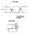
- This situation is shown more generalized in Figs. 8A and 8B.
- Since there is a phase difference between a signal S and an inverted signal ^S thereof, the point at which the two signals intersect is not on a center value of the amplitude.
- When the intersecting point is at a potential lower than the center value, it is regarded that both of S and ^S have a logic value "0" in terms of the logic circuit. Similarly, when the intersecting point is at a potential higher than the center value, it is regarded that the two are "1".
- Under the situation where S = ^S, both of the two selectors configured by two CMOS transmission gates become ON.
- When the two input signals are different from each other at this time, a logic collision occurs. there is an electrical short-circuit, and a current flows. Such a phenomenon is generally known as "wraparound of the signal".
- Figure 9 and Fig. 10 are diagrams of the results of simulation in the cases of conventional 8tr type and 6tr type EXOR logic circuits having inverters for inverting the input signals and passing the outputs thereof through one inverter.
- As apparent from the diagrams, in the conventional 8tr type and 6tr type EXOR logic circuits, phase differences arise between the two outputs and therefore the intersecting points are not at the center values of the amplitudes.
- Further, the 4tr type EXOR and EXNOR logic circuits each configured by four transistors seem to be superior to the 6tr type logic circuit at a glance, but are not superior in actuality.
- In Fig. 5, when A = 0 and B = 0, the two PMOS transistors PT51 and PT52 become ON, and a logic potential "0" is transferred to the output through the two PMOS transistors PT51 and PT52.
- However, the PMOS transistors PT51 and PT52 cannot completely transfer the logic potential "0" and therefore a potential which has become higher by the amount of the threshold value of the PMOS transistors appears at the output.
- On the other hand, in Fig. 6, when A = 1 and B = 1, the two PMOS transistors PT61 and PT62 cut off, the two NMOS transistors NT61 and NT62 become ON, and a logic potential "1" is transferred to the output through the two NMOS transistors NT61 and NT62.
- However, the NMOS transistors NT61 and NT62 cannot completely transfer the logic potential "1" and therefore a potential which has become lower by the amount of the threshold value of the NMOS transistors appears at the output.
- Signals of such incomplete logic potentials exert a serious influence upon a low voltage operation margin and noise margin. For this reason, in actuality, it is necessary to provide and use inverters INV51 and INV61 as buffers for restoration of the potential as shown in Fig. 11 and Fig. 12.
- The present invention was made in consideration with such a circumstance and has as an object thereof to provide a logic circuit capable of suppressing an occurrence of wraparound of a signal, capable of reducing the power consumption, and achieving a reduction of circuit scale and an improvement of operating speed and a full adder using the same.
- According to a first aspect of the present invention, there is provided a logic circuit, comprising an exclusive-OR generation circuit for receiving a first logic signal and a second logic signal taking a first or second level and generating an exclusive-OR of the first logic signal and second logic signal, a dual signal generation circuit for receiving the first logic signal and the second logic signal taking the first or second level and generating a dual signal of the exclusive-OR of the first logic signal and second logic signal, and an interpolation circuit for compulsorily setting an output level of said dual signal at the first level when the output level of said exclusive-OR is the second level.
- According to a second aspect of the present invention, there is provided a logic circuit, comprising an exclusive-OR generation circuit for receiving a first logic signal and a second logic signal taking a first or second level and generating an exclusive-OR of the first logic signal and second logic signal, a dual signal generation circuit for receiving the first logic signal and the second logic signal taking the first or second level and generating a dual signal of the exclusive-OR of the first logic signal and second logic signal, and an interpolation circuit for compulsorily setting the output level of said exclusive-OR at the second level when the output level of said dual signal is the first level.
- According to a third aspect of the present invention, there is provided a logic circuit, comprising an exclusive-OR generation circuit for receiving a first logic signal and a second logic signal taking a first or second level and generating an exclusive-OR of the first logic signal and second logic signal, a dual signal generation circuit for receiving the first logic signal and the second logic signal taking the first or second level and generating a dual signal of the exclusive-OR of the first logic signal and second logic signal, and an interpolation circuit for compulsorily setting an output level of said dual signal at the first level when the output level of said exclusive-OR is the second level, while compulsorily setting the output level of said exclusive-OR at the second level when the output level of said dual signal is the first level.
- According to a fourth aspect of the present invention, there is provided a logic circuit, comprising a first input terminal with a first logic signal taking a first or second level input thereto; a second input terminal with a second logic signal taking a first or second level input thereto; a first output terminal for outputting an exclusive-OR; a second output terminal for outputting a dual signal of said exclusive-OR; a dual signal generation circuit having first conductivity type first and second transistors connected in series between said first level use power supply potential and said second output terminal, turning ON when the signal of second level is supplied to the control terminal, while cutting off when the signal of first level is supplied, a second conductivity type first transistor connected between said first input terminal and said second output terminal, turning ON when the signal of first level is supplied to the control terminal, while cutting off when the signal of second level is supplied, and a second conductivity type second transistor connected between said second input terminal and said second output terminal, turning on when the signal of first level is supplied to the control terminal, while cutting off when the signal of second level is supplied; an exclusive-OR generation circuit having a first conductivity type third transistor connected between said first input terminal and said first output terminal. turning ON when the signal of second level is supplied to the control terminal, while cutting off when the signal of first level is supplied, a first conductivity type fourth transistor connected between said second input terminal and said first output terminal, turning on when the signal of second level is supplied to the control terminal, while cutting off when the signal of first level is supplied, and second conductivity type third and fourth transistors connected in series between said second level use power supply potential and said first output terminal, turning on when the signal of first level is supplied to the control terminal, while cutting off when the signal of second level is supplied; and an interpolation circuit having a first conductivity type fifth transistor connected in series between said first level use power supply potential and said second output terminal, turning on when the signal of second level is supplied to the control terminal, while cutting off when the signal of first level is supplied, and a second conductivity type fifth transistor connected in series between said second level use power supply potential and said first output terminal, turning on when the signal of first level is supplied to the control terminal, while cutting off when the signal of second level is supplied, wherein the control terminals of said first conductivity type second and fourth transistors and second conductivity type second and third transistors are connected to said first input terminal; the control terminals of said first conductivity type first and third transistors and second conductivity type first and fourth transistors are connected to said second input terminal; the control terminal of said first conductivity type fifth transistor is connected to said first output terminal; and the control terminal of said second conductivity type fifth transistor is connected to said second output terminal.
- According to a fifth aspect of the present invention, there is provided a full adder, comprising a logic circuit having an exclusive-OR generation circuit for receiving a first logic signal and a second logic signal taking a first or second level and generating an exclusive-OR of the first logic signal and second logic signal, a dual signal generation circuit for receiving the first logic signal and the second logic signal taking the first or second level and generating a dual signal of the exclusive-OR of the first logic signal and second logic signal, and an interpolation circuit for compulsorily setting an output level of said dual signal at the first level when the output level of said exclusive-OR is the second level, a sum signal generation circuit for generating a sum signal based on an exclusive-OR output and a dual signal output of said logic circuit, and a carry signal generation circuit for generating a carry signal by selecting said first logic signal or carry signal based on the exclusive-OR output and the dual signal output of said logic circuit.
- According to a sixth aspect of the present invention, there is provided a full adder, comprising a logic circuit having an exclusive-OR generation circuit for receiving a first logic signal and a second logic signal taking a first or second level and generating an exclusive-OR of the first logic signal and second logic signal, a dual signal generation circuit for receiving the first logic signal and the second logic signal taking the first or second level and generating a dual signal of the exclusive-OR of the first logic signal and second logic signal, and an interpolation circuit for compulsorily setting the output level of said exclusive-OR at the second level when the output level of said dual signal is the first level; a sum signal generation circuit for generating a sum signal based on then exclusive-OR output and the dual signal output of said logic circuit; and a carry signal generation circuit for generating a carry signal by selecting said first logic signal or carry signal based on the exclusive-OR output and the dual signal output of said logic circuit.
- According to a seventh aspect of the present invention, there is provided a full adder, comprising a logic circuit having an exclusive-OR generation circuit for receiving a first logic signal and a second logic signal taking a first or second level and generating an exclusive-OR of the first logic signal and second logic signal, a dual signal generation circuit for receiving the first logic signal and the second logic signal taking the first or second level and generating a dual signal of the exclusive-OR of the first logic signal and second logic signal, and an interpolation circuit for compulsorily setting an output level of said dual signal at the first level when the output level of said exclusive-OR is the second level, while compulsorily setting the output level of said exclusive-OR at the second level when the output level of said dual signal is the first level; a sum signal generation circuit for generating a sum signal based on an exclusive-OR output and a dual signal output of said logic circuit; and a carry signal generation circuit for generating a carry signal by selecting said first logic signal or carry signal based on the exclusive-OR output and the dual signal output of said logic circuit.
- According to a eighth aspect of the present invention, there is provided a full adder, comprising a logic circuit having a first input terminal with a first logic signal taking a first or second level input thereto, a second input terminal with a second logic signal taking a first or second level input thereto, a first output terminal for outputting an exclusive-OR, a second output terminal for outputting a dual signal of said exclusive-OR, a dual signal generation circuit which has first conductivity type first and second transistors connected in series between said first level use power supply potential and said second output terminal, turning ON when the signal of second level is supplied to the control terminal, while cutting off when the signal of first level is supplied, a second conductivity type first transistor connected between said first input terminal and said second output terminal, turning ON when the signal of first level is supplied to the control terminal, while cutting off when the signal of second level is supplied, and a second conductivity type second transistor connected between said second input terminal and said second output terminal, turning on when the signal of first level is supplied to the control terminal, while cutting off when the signal of second level is supplied, an exclusive-OR generation circuit which has a first conductivity type third transistor connected between said first input terminal and said first output terminal, turning ON when the signal of second level is supplied to the control terminal, while cutting off when the signal of first level is supplied, a first conductivity type fourth transistor connected between said second input terminal and said first output terminal, turning on when the signal of second level is supplied to the control terminal, while cutting off when the signal of first level is supplied, and second conductivity type third and fourth transistors connected in series between said second level use power supply potential and said first output terminal, turning on when the signal of first level is supplied to the control terminal, while cutting off when the signal of second level is supplied, and an interpolation circuit which has a first conductivity type fifth transistor connected in series between said first level use power supply potential and said second output terminal, turning on when the signal of second level is supplied to the control terminal, while cutting off when the signal of first level is supplied, and a second conductivity type fifth transistor connected in series between said second level use power supply potential and said first output terminal, turning on when the signal of first level is supplied to the control terminal, while cutting off when the signal of second level is supplied. wherein the control terminals of said first conductivity type second and fourth transistors and second conductivity type second and third transistors are connected to said first input terminal, the control terminals of said first conductivity type first and third transistors and second conductivity type first and fourth transistors are connected to said second input terminal, the control terminal of said first conductivity type fifth transistor is connected to said first output terminal, and the control terminal of said second conductivity type fifth transistor is connected to said second output terminal; a sum signal generation circuit for generating a sum signal based on an exclusive-OR output and a dual signal output of said logic circuit; and a carry signal generation circuit for generating a carry signal by selecting said first logic signal or carry signal based on the exclusive-OR output and the dual signal output of said logic circuit.
- Further, in the present invention, said first conductivity type first, second, third, fourth, and fifth transistors are p-channel field effect transistors, and said second conductivity type first, second, third, fourth, and fifth transistors are n-channel field effect transistors.
- According to the logic circuit of the present invention, the exclusive-OR (EXOR = A(+)B) and the dual signal thereof (EXNOR = A^(+)B) are approximately simultaneously generated without generating an inversion of the two first and second input logic signals A and B.
- At this time, in accordance with for example the level of the input signal, when the output level of the exclusive-OR is the second level, the output level of the dual signal is compulsorily set at the first level by the interpolation circuit.
- Further, when the output level of the dual signal is the first level, the output level of the exclusive-OR is compulsorily set at the second level.
- Further, according to the full adder of the present invention, the dual signal is generated in the logic circuit and supplied to the carry signal generation circuit.
- Accordingly, an inverter for inverting the logic as in the conventional circuit is unnecessary. As a result, the occurrence of wraparound of the signal is suppressed.
- These and other objects and features of the present invention will become clearer from the following description of the preferred embodiments given with reference to the accompanying drawings, in which:
- Fig. 1 is a circuit diagram of an example of the configuration of an 8tr type EXOR logic circuit;
- Fig. 2 is a circuit diagram of an example of the configuration of an 8tr type EXNOR logic circuit;
- Fig. 3 is a circuit diagram of an example of the configuration of a 6tr type EXOR logic circuit;
- Fig. 4 is a circuit diagram of an example of the configuration of a 6tr type EXNOR logic circuit;
- Fig. 5 is a circuit diagram of an example of the configuration of a 4tr type EXOR logic circuit;
- Fig. 6 is a circuit diagram of an example of the configuration of a 4tr type EXNOR logic circuit;
- Fig. 7 is a circuit diagram of an example of the configuration of a carry generation circuit of the full adder;
- Fig. 8A and 8B are diagrams for explaining the problem of the circuit of Fig. 7;
- Fig. 9 is a diagram of the results of simulation in the case of an 8tr type EXOR logic circuit having an inverter for inverting the input signals and passing the output thereof through one inverter;
- Fig. 10 is a diagram of the results of simulation in the case of an 6tr type EXOR logic circuit having an inverter for inverting the input signals and passing the output thereof through one inverter;
- Fig. 11 is a diagram for explaining the problem of a 4tr type logic circuit;
- Fig. 12 is a diagram for explaining the problem of a 4tr type logic circuit;
- Fig. 13 is a circuit diagram of an embodiment of an EXOR/EXNOR logic circuit according to the present invention;
- Fig. 14 is a diagram for explaining an operation of the circuit of Fig. 13 when A = B = 0.
- Fig. 15 is a diagram for explaining an operation of the circuit of Fig. 13 when A = 0 and B = 1;
- Fig. 16 is a diagram for explaining an operation of the circuit of Fig. 13 when A = 1 and B = 0;
- Fig. 17 is a diagram for explaining an operation of the circuit of Fig. 13 when A = 1 and B = 1.
- Fig. 18 is a diagram of the results of simulation of the circuit of Fig. 13; and
- Fig. 19 is a circuit diagram of an example of the configuration of a full adder using the EXOR/EXNOR logic circuit according to the present invention.
-
- Below, preferred embodiments will be described with reference to the accompanying drawings.
- Figure 13 is a circuit diagram of an embodiment of an EXOR/EXNOR logic circuit according to the present invention.
- This EXOR/
EXNOR logic circuit 10 comprises PMOS transistors PT101 to PT105 as first conductivity type (p-channel) first to fifth transistors, NMOS transistors NT101 to NT105 as second conductivity type (n-channel) first to fifth transistors, a first input terminal TIN101 for the first logic signal A, a second input terminal TIN102 for the second logic signal B, a first output terminal TOT101 for the exclusive-OR A(+)B, and a second output terminal TOT102 for the dual signal A^(+)B of the exclusive-OR A(+)B. - Among these configuration elements, a dual
signal generation circuit 11 is configured by the PMOS transistors PT101 and PT102 and the NMOS transistors NT101 and NT102, an exclusive-OR circuit 12 is configured by the PMOS transistors PT103 and PT104 and the NMOS transistors NT103 and NT104, and aninterpolation circuit 13 is configured by the PMOS transistor PT105 and the NMOS transistor NT105. - In this way, the EXOR/
EXNOR logic circuit 10 according to the present invention uses 10 transistors of the PMOS transistors PT101 to PT105 and the NMOS transistors NT101 to NT105 as the main configuration elements. There is no inverter for inverting the input signal as seen in the conventional 8tr and 6tr type logic circuits. - The PMOS transistor PT103 is connected between the input terminal TIN101 of the logic signal A and the output terminal TOT101 of the exclusive-OR A(+)B, and the PMOS transistor PT104 is connected between the input terminal TIN 102 of the logic signal B and the output terminal TOT101.
- The NMOS transistor NT101 is connected between the input terminal TIN101 of the logic signal A and the output terminal TOT102 of the dual signal A^(+)B of the exclusive-OR A(+)B, and the NMOS transistor NT102 is connected between the input terminal TIN102 of the logic signal B and the output terminal TOT102.
- Further, the PMOS transistors PT101 and PT102 are connected in series between the supply line of the power supply voltage VDD and the output terminal TOT102, and the PMOS transistor PT105 is connected between the supply line of the power supply voltage VDD and the output terminal TOT102 in parallel to this.
- Further, the NMOS transistors NT103 and NT104 are connected in series between the output terminal TOT101 and the ground GND, and the NMOS transistor NT105 is connected between the output terminal TOT101 and the ground GND in parallel to this.
- Further, the gates of the PMOS transistors PT102 and PT104 and the gates of the NMOS transistors NT102 and NT103 are connected to the input terminal TIN 101, and the gates of the PMOS transistors PT101 and PT103 and the gates of the NMOS transistors NT101 and NT104 are connected to the input terminal TIN102.
- Further, the gate of the PMOS transistor PT105 is connected to the output terminal TOT101, and the gate of the NMOS transistor NT105 is connected to the output terminal TOT102.
- Next, the operation by the above configuration will be explained with reference to Fig. 14 to Fig. 17.
- Figure 14 is a view for explaining the operation in a case where the logic signals A = 0 and B = 0, Fig. 15 is a view for explaining the operation in a case where A = 0 and B = 1, Fig. 16 is a view for explaining the operation in a case where A = 1 and B = 0, and Fig. 17 is a view for explaining the operation in a case where A = 1 and B = 1.
- Note that, transistors given the marks x in the figures show the cut off state. Further, arrows indicate charge and discharge routes of the output contacts.
- When A = 0 and B = 0, as shown in Fig. 14, the PMOS transistors PT101 to PT105 turn ON, and the NMOS transistors NT101 to NT104 cut off.
- By this, the potential of the output terminal TOT102 is pulled up to the power supply voltage VDD level, and the dual signal output A^(+)B becomes a logic "1".
- Further, by the PMOS transistors PT103 and PT104, the exclusive-OR A(+)B output from the output terminal TOT101 can start to change to a logic "0".
- At this time, due to the PMOS transistors PT103 and PT104, the logic does not become a complete "0", but the NMOS transistor NT105 connected to the output terminal TOT102 with the gate pulled up to the power supply voltage VDD with a slight delay turns ON. By this, the output terminal TOT101 is pulled into the ground level, and the exclusive-OR A(+)B reaches the logic "0".
- Further, by the pull-in of the output terminal TOT101 to the ground level, the PMOS transistor PT105 with the gate connected to the output terminal TOT101 completely tunis ON, and, by this, the dual signal output A^(+)B is stably kept at the logic "1".
- When A = 0 and B = 1, as shown in Fig. 15, the PMOS transistors PT102 and PT104 and the NMOS transistors NT101 and NT104 turn ON, and the PMOS transistors PT101, PT103, and PT105 and the NMOS transistors NT102, NT103, and NT105 cut off.
- Then, the potential of the output terminal TOT102 is pulled into the logic "0" level, that is, the ground level (0V), through the NMOS transistor NT101 and the input terminal TIN101, and the dual signal output A^(+)B becomes the logic "0".
- Further, the signal B input to the input terminal TIN102 through the PMOS transistor PT104 having the logic "I", that is, the power supply voltage VDD level, is propagated to the output terminal TOT101, and as a result, the exclusive-OR output A(+)B reaches the logic "1".
- When A = 1 and B = 0, as shown in Fig. 16, the PMOS transistors PT101 and PT103 and the NMOS transistors NT102 and NT103 turn ON, and the PMOS transistors PT102, PT104, and PT105 and the NMOS transistors NT101, NT104, and NT105 cut off.
- Then, the potential of the output terminal TOT102 is pulled into the logic "0" level, that is, the ground level (0V), through the NMOS transistor NT102 and the input terminal TIN102, and the dual signal output A^(+)B becomes the logic "0".
- Further, the signal A input to the input terminal TIN 101 through the PMOS transistor PT103 having the logic "1", that is, the power supply voltage VDD level, is propagated to the output terminal TOT101, and as a result, the exclusive-OR output A(+)B reaches the logic "1".
- When A = 1 and B = 1, as shown in Fig. 17, the NMOS transistors NT101 to NT105 turn ON, and the PMOS transistors PT101 to PT104 cut off.
- Along with the turning ON of the NMOS transistors NT103, NT104 and NT105, the output terminal TOT101 is pulled into the ground level. the exclusive-OR output A(+)B becomes the logic "0".
- Further, the signals A and B of the logic "1" input to the input terminals TIN101 and TIN102 through the NMOS transistors NT101 and NT102 are propagated to the output terminal TOT102, and the dual signal output A^(+)B can start to change to the logic "1".
- At this time, if the signals are passed through the NMOS transistors NT101 and NT102, they do not become completely "I", but the PMOS transistor PT105 connected to the output terminal TOT101 with the gate pulled into the ground level turns ON with a slight delay. By this, the output terminal TOT102 is pulled up to the power supply voltage VDD level through the PMOS transistor PT105, and the dual signal output A^(+)B reaches the logic "1".
- In this way, the routes reaching the outputs A^(+)B and A(+)B from the change of the input signal are substantially equal. For this reason, there is almost no phase difference created between the two output signals.
- Figure 18 is a diagram of the results of simulation of the circuit of Fig. 13.
- In Fig. 18, a curve indicated by a solid line shows the input logic signal A, a curve indicated by a broken line shows the input logic signal B, a curve indicated by a solid line with triangles shows the exclusive-OR output (EXOR), and a curve indicated by a solid line with squares shows the dual signal output (EXNOR).
- As explained with reference to Fig. 9 and Fig. 10, in each of the 8tr type and 6tr type logic circuits based on the related art, a phase difference is created between the two outputs, and the intersecting point is not at the center value of the amplitude.
- Contrary to this, according to the logic circuit according to the present invention, as apparent from Fig. 18, the intersecting point of two output waveforms is substantially at the center value.
- Accordingly, according to the circuit of the present invention, even in a case where two input signals are different from each other, an occurrence of logic collision is prevented, no current due to short-circuiting flows, and a "signal wraparound" phenomenon can be suppressed.
- Further, in Fig. 18, while slight, excellence in terms of speed is also shown. The circuit scale is 10 transistors including the amount of the inverter. Excellent characteristics can be realized without a large increase in the number of elements compared with the related art.
- As explained above, according to the present embodiment, since provision is made of the exclusive-OR generation circuit 12 for receiving the first logic signal A and the second logic signal B taking the logic "1" or "0" and generating the exclusive-OR of the first logic signal A and the second logic signal B, the dual
signal generation circuit 11 for receiving the first logic signal A and the second logic signal B and generating the dual signal of the exclusive-OR of the first logic signal A and the second logic signal B, and theinterpolation circuit 13 for compulsorily setting the output level of the dual signal at the level of the logic "1" when the output level of the exclusive-OR is the logic "0", while compulsorily setting the output level of the exclusive-OR at the level of the logic "0" when the output level of the dual signal is the logic "1", the occurrence of wraparound of the signal can be suppressed and the power consumption can be reduced. - Further, there is an advantage that a reduction of the circuit scale can be achieved and, in addition, an improvement of the operating speed can be achieved.
- Figure 19 is a circuit diagram of an example of the configuration of a full adder using the EXOR/EXNOR logic circuit according to the present invention.
- A
full adder 20 is configured by using the EXOR/EXNOR logic circuit 10 of Fig. 13 and connecting asum generation circuit 21 and a carrysignal generation circuit 22 to the output side thereof and is characterized in that there is no inverter for the inversion of the EXOR output unlike that according to the related art. - Further, the
full adder 20 comprises an input terminal TIN201 of the logic signal A, an input terminal TIN202 of the logic signal B, an output terminal TOT201 of a sum signal S [= A (+) B (+) C], and an output terminal TOT202 of the carry signal CO (= AB + BC + CA). - The sum
signal generation circuit 21 is configured by a PMOS transistor PT211, an NMOS transistor NT211, and a transmission gate TMG211. - The PMOS transistor PT211 is connected between the output terminal TOT101 of the EXOR/
EXNOR logic circuit 10 and the output terminal TOT201 of the sum signal, and its gate is connected to one input/output terminal of the transmission gate TMG211. - The NMOS transistor NT211 is connected between the output terminal TOT102 of the EXOR/
EXNOR logic circuit 10 and the output terminal TOT201 of the sum signal, and its gate is connected to one input/output terminal of the transmission gate TMG211. - A gate of the PMOS transistor of the transmission gate TMG211 is connected to the output terminal TOT101 of the EXOR/
EXNOR logic circuit 10, a gate of the NMOS transistor is connected to the output terminal TOT102 of the EXOR/EXNOR logic circuit 10, and the other input/output terminal is connected to the output terminal TOT201 of the sum signal. - The carry
signal generation circuit 22 is configured by CMOS transmission gates TMG221 and TMG222. - One input/output terminal of the transmission gate TMG221 is connected to the input terminal TIN201 of the logic signal A, and the other input/output terminal is connected to the output terminal TOT202 of the carry over signal CO.
- A gate of the PMOS transistor of the transmission gate TMG221 is connected to the output terminal TOT101 of the EXOR/
EXNOR logic circuit 10, and a gate of the NMOS transistor is connected to the output terminal TOT102 of the EXOR/EXNOR logic circuit 10. - Further, one input/output terminal of the transmission gate TMG222 is connected to an input terminal TIN203 of the carry signal C, and the other input terminal is connected to the output terminal TOT202 of the carry over signal CO.
- A gate of the PMOS transistor of the transmission gate TMG222 is connected to the output terminal TOT102 of the EXOR/
EXNOR logic circuit 10, and a gate of the NMOS transistor is connected to the output terminal TOT101 of the EXOR/EXNOR logic circuit 10. - In the
full adder 20 having such a configuration, when the input logic signal A = B = 0, as shown in Fig. 14, the exclusive-OR output A(+)B becomes equal to 0, and the dual signal output A^(+)B thereof becomes equal to 1. - By this, in the sum
signal generation circuit 21, the transmission gate TMG211 becomes the conductive state, the PMOS transistor PT211 or the NMOS transistor NT211 turns ON in accordance with the potential of the output terminal TOT201, the signal of the logic "0" is propagated through the PMOS transistor PT211 to the output terminal TOT201, or the signal of the logic "1" is propagated through the NMOS transistor NT211 to the output terminal TOT201. - Further, in the carry
signal generation circuit 22, the transmission gate TMG221 is held in the conductive state, and the transmission gate TMG222 is held in the nonconductive state. As a result, the signal of the logic "0" input to the input terminal TIN201 is propagated to the output terminal TOT202. - When the input logic signals A = 0 and B = 1, as shown in Fig. 15, the exclusive-OR output A(+)B becomes equal to 1, and the dual signal output A^(+)B thereof becomes equal to 0.
- By this, in the sum
signal generation circuit 21, the transmission gate TMG211 is held in the nonconductive state. - Further, in the carry
signal generation circuit 22, the transmission gate TMG221 is held in the nonconductive state, and the transmission gate TMG222 is held in the conductive state. As a result, the carry signal C of the input terminal TIN203 is propagated to the output terminal TOT202. - When the input logic signals A = I and B = 0, as shown in Fig. 16, the exclusive-OR output A(+)B becomes equal to 1, and the dual signal output A^(+)B thereof becomes equal to 0.
- By this, in the sum
signal generation circuit 21, the transmission gate TMG211 is held in the nonconductive state. - Further, in the carry
signal generation circuit 22, the transmission gate TMG221 is held in the nonconductive state, and the transmission gate TMG222 is held in the conductive state. As a result, the carry signal C of the input terminal TIN203 is propagated to the output terminal TOT202. - When the input logic signals A = B = 1, as shown in Fig. 17, the exclusive-OR output A(+)B becomes equal to 0, and the dual signal output A^(+)B thereof becomes equal to 1.
- By this, in the sum
signal generation circuit 21, the transmission gate TMG211 becomes the conductive state, the PMOS transistor PT211 or the NMOS transistor NT211 turns ON in accordance with the potential of the output terminal TOT201, the signal of the logic "0" is propagated through the PMOS transistor PT211 to the output terminal TOT201, or the signal of the logic "1" is propagated through the NMOS transistor NT211 to the output terminal TOT201. - Further, in the carry
signal generation circuit 22, the transmission gate TMG221 is held in the conductive state, and the transmission gate TMG222 is held in the nonconductive state. As a result, the signal of the logic "0" input to the input terminal TIN201 is propagated to the output terminal TOT202. - According to the
full adder 20, the dual signal of EXOR is generated in the EXOR/EXNOR logic circuit 10 and supplied to the carry signal generation circuit. therefore the current generated due to wraparound of the signal can be suppressed and the power consumption can be reduced. - Summarizing the effects of the invention, as explained above, according to the present invention, the occurrence of wraparound of the signal can be suppressed and the power consumption can be reduced.
- Further, there is an advantage that a reduction of the circuit scale can be achieved and in addition an improvement of the operating speed can be achieved.
- Note that the present invention is not limited to the above embodiments and includes modifications within the scope of the claims.
Claims (10)
- A logic circuit, comprising:an exclusive-OR generation circuit (12) for receiving a first logic signal and a second logic signal taking a first or second level and generating an exclusive-OR of the first logic signal and second logic signal,a dual signal generation circuit (11) for receiving the first logic signal and the second logic signal taking the first or second level and generating a dual signal of the exclusive-OR of the first logic signal and second logic signal, andan interpolation circuit (13) for compulsorily setting an output level of said dual signal at the first level when the output level of said exclusive-OR is the second level.
- A logic circuit, comprising:an exclusive-OR generation circuit (12) for receiving a first logic signal and a second logic signal taking a first or second level and generating an exclusive-OR of the first logic signal and second logic signal,a dual signal generation circuit (11) for receiving the first logic signal and the second logic signal taking the first or second level and generating a dual signal of the exclusive-OR of the first logic signal and second logic signal, andan interpolation circuit (13) for compulsorily setting the output level of said exclusive-OR at the second level when the output level of said dual signal is the first level.
- A logic circuit, comprising:an exclusive-OR generation circuit (12) for receiving a first logic signal and a second logic signal taking a first or second level and generating an exclusive-OR of the first logic signal and second logic signal,a dual signal generation circuit (11) for receiving the first logic signal and the second logic signal taking the first or second level and generating a dual signal of the exclusive-OR of the first logic signal and second logic signal, andan interpolation circuit (13) for compulsorily setting an output level of said dual signal at the first level when the output level of said exclusive-OR is the second level, while compulsorily setting the output level of said exclusive-OR at the second level when the output level of said dual signal is the first level.
- A logic circuit (10), comprising:a first input terminal with a first logic signal taking a first or second level input thereto,a second input terminal with a second logic signal taking a first or second level input thereto.a first output terminal for outputting an exclusive-OR,a second output terminal for outputting a dual signal of said exclusive-OR,a dual signal generation circuit (11) havingfirst conductivity type first and second transistors connected in series between said first level use power supply potential and said second output terminal, turning ON when the signal of second level is supplied to the control terminal, while cutting off when the signal of first level is supplied,a second conductivity type first transistor connected between said first input terminal and said second output terminal, turning ON when the signal of first level is supplied to the control terminal, while cutting off when the signal of second level is supplied, anda second conductivity type second transistor connected between said second input terminal and said second output terminal, turning on when the signal of first level is supplied to the control terminal, while cutting off when the signal of second level is supplied,an exclusive-OR generation circuit (12) havinga first conductivity type third transistor connected between said first input terminal and said first output terminal, turning ON when the signal of second level is supplied to the control terminal, while cutting off when the signal of first level is supplied,a first conductivity type fourth transistor connected between said second input terminal and said first output terminal, turning on when the signal of second level is supplied to the control terminal, while cutting off when the signal of first level is supplied, andsecond conductivity type third and fourth transistors connected in series between said second level use power supply potential and said first output terminal, turning on when the signal of first level is supplied to the control terminal, while cutting off when the signal of second level is supplied, andan interpolation circuit (13) havinga first conductivity type fifth transistor connected in series between said first level use power supply potential and said second output terminal, turning on when the signal of second level is supplied to the control terminal, while cutting off when the signal of first level is supplied, anda second conductivity type fifth transistor connected in series between said second level use power supply potential and said first output terminal, turning on when the signal of first level is supplied to the control terminal, while cutting off when the signal of second level is supplied, whereinthe control terminals of said first conductivity type second and fourth transistors and second conductivity type second and third transistors are connected to said first input terminal,the control terminals of said first conductivity type first and third transistors and second conductivity type first and fourth transistors are connected to said second input terminal,the control terminal of said first conductivity type fifth transistor is connected to said first output terminal, andthe control terminal of said second conductivity type fifth transistor is connected to said second output terminal.
- A logic circuit (10) as set forth in claim 4, wherein:said first conductivity type first, second, third, fourth, and fifth transistors are p-channel field effect transistors, andsaid second conductivity type first, second, third, fourth, and fifth transistors are n-channel field effect transistors.
- A full adder (20), comprising:a logic circuit havingan exclusive-OR generation circuit (12) for receiving a first logic signal and a second logic signal taking a first or second level and generating an exclusive-OR of the first logic signal and second logic signal,a dual signal generation circuit (11) for receiving the first logic signal and the second logic signal taking the first or second level and generating a dual signal of the exclusive-OR of the related first logic signal and second logic signal, andan interpolation circuit (13) for compulsorily setting an output level of said dual signal at the first level when the output level of said exclusive-OR is the second level,a sum signal generation circuit (21) for generating a sum signal based on an exclusive-OR output and a dual signal output of said logic circuit, anda carry signal generation circuit (22) for generating a carry signal by selecting said first logic signal or carry signal based on the exclusive-OR output and the dual signal output of said logic circuit.
- A full adder (20), comprising:a logic circuit (10) havingan exclusive-OR generation circuit (12) for receiving a first logic signal and a second logic signal taking a first or second level and generating an exclusive-OR of the first logic signal and second logic signal, a dual signal generation circuit (11) for receiving the first logic signal and the second logic signal taking the first or second level and generating a dual signal of the exclusive-OR of the first logic signal and second logic signal, andan interpolation circuit (13) for compulsorily setting the output level of said exclusive-OR at the second level when the output level of said dual signal is the first level;a sum signal generation circuit (21) for generating a sum signal based on then exclusive-OR output and the dual signal output of said logic circuit; anda carry signal generation circuit (22) for generating a carry signal by selecting said first logic signal or carry signal based on the exclusive-OR output and the dual signal output of said logic circuit.
- A full adder (20), comprising :a logic circuit (10) havingan exclusive-OR generation circuit (12) for receiving a first logic signal and a second logic signal taking a first or second level and generating an exclusive-OR of the first logic signal and second logic signal,a dual signal generation circuit (11) for receiving the first logic signal and the second logic signal taking the first or second level and generating a dual signal of the exclusive-OR of the first logic signal and second logic signal, andan interpolation circuit (13) for compulsorily setting an output level of said dual signal at the first level when the output level of said exclusive-OR is the second level, while compulsorily setting the output level of said exclusive-OR at the second level when the output level of said dual signal is the first level;a sum signal generation circuit (21) for generating a sum signal based on an exclusive-OR output and a dual signal output of said logic circuit; anda carry signal generation circuit (22) for generating a carry signal by selecting said first logic signal or carry signal based on the exclusive-OR output and the dual signal output of said logic circuit.
- A full adder (20), comprising :a logic circuit (10) havinga first input terminal with a first logic signal taking a first or second level input thereto,a second input terminal with a second logic signal taking a first or second level input thereto,a first output terminal for outputting an exclusive-OR,a second output terminal for outputting a dual signal of said exclusive-OR,a dual signal generation circuit (11) which hasfirst conductivity type first and second transistors connected in series between said first level use power supply potential and said second output terminal, turning ON when the signal of second level is supplied to the control terminal, while cutting off when the signal of first level is supplied,a second conductivity type first transistor connected between said first input terminal and said second output terminal, turning ON when the signal of first level is supplied to the control terminal, while cutting off when the signal of second level is supplied, anda second conductivity type second transistor connected between said second input terminal and said second output terminal, turning on when the signal of first level is supplied to the control terminal, while cutting off when the signal of second level is supplied,an exclusive-OR generation circuit (12) which hasa first conductivity type third transistor connected between said first input terminal and said first output terminal, turning ON when the signal of second level is supplied to the control terminal, while cutting off when the signal of first level is supplied.a first conductivity type fourth transistor connected between said second input terminal and said first output terminal, turning on when the signal of second level is supplied to the control terminal, while cutting off when the signal of first level is supplied, andsecond conductivity type third and fourth transistors connected in series between said second level use power supply potential and said first output terminal, turning on when the signal of first level is supplied to the control terminal, while cutting off when the signal of second level is supplied, andan interpolation circuit (13) which hasa first conductivity type fifth transistor connected in series between said first level use power supply potential and said second output terminal, turning on when the signal of second level is supplied to the control terminal, while cutting off when the signal of first level is supplied, anda second conductivity type fifth transistor connected in series between said second level use power supply potential and said first output terminal, turning on when the signal of first level is supplied to the control terminal, while cutting off when the signal of second level is supplied, whereinthe control terminals of said first conductivity type second and fourth transistors and second conductivity type second and third transistors are connected to said first input terminal,the control terminals of said first conductivity type first and third transistors and second conductivity type first and fourth transistors are connected to said second input terminal,the control terminal of said first conductivity type fifth transistor is connected to said first output terminal, andthe control terminal of said second conductivity type fifth transistor is connected to said second output terminal;a sum signal generation circuit (21) for generating a sum signal based on an exclusive-OR output and a dual signal output of said logic circuit; anda carry signal generation circuit (22) for generating a carry signal by selecting said first logic signal or carry signal based on the exclusive-OR output and the dual signal output of said logic circuit.
- A full adder (20) as set forth in claim 9, wherein:said first conductivity type first, second, third, fourth, and fifth transistors are p-channel field effect transistors, andsaid second conductivity type first, second, third, fourth, and fifth transistors are n-channel field effect transistors.
Applications Claiming Priority (2)
| Application Number | Priority Date | Filing Date | Title |
|---|---|---|---|
| JP34538399A JP2001168707A (en) | 1999-12-03 | 1999-12-03 | Logic circuit and full adder using the same |
| JP34538399 | 1999-12-03 |
Publications (1)
| Publication Number | Publication Date |
|---|---|
| EP1111791A1 true EP1111791A1 (en) | 2001-06-27 |
Family
ID=18376235
Family Applications (1)
| Application Number | Title | Priority Date | Filing Date |
|---|---|---|---|
| EP00403396A Withdrawn EP1111791A1 (en) | 1999-12-03 | 2000-12-04 | Logic circuit and full adder using the same |
Country Status (3)
| Country | Link |
|---|---|
| US (1) | US6700405B1 (en) |
| EP (1) | EP1111791A1 (en) |
| JP (1) | JP2001168707A (en) |
Cited By (2)
| Publication number | Priority date | Publication date | Assignee | Title |
|---|---|---|---|---|
| US7560955B2 (en) | 2004-11-24 | 2009-07-14 | Nec Electronics Corporation | Logic circuit |
| CN104166536A (en) * | 2014-07-17 | 2014-11-26 | 南京航空航天大学 | Low-load mirror image summator |
Families Citing this family (31)
| Publication number | Priority date | Publication date | Assignee | Title |
|---|---|---|---|---|
| KR100437841B1 (en) * | 2002-01-02 | 2004-06-30 | 주식회사 하이닉스반도체 | half adder circuit |
| US7260595B2 (en) * | 2002-12-23 | 2007-08-21 | Arithmatica Limited | Logic circuit and method for carry and sum generation and method of designing such a logic circuit |
| GB2401962B (en) * | 2003-05-23 | 2005-05-18 | Arithmatica Ltd | A sum bit generation circuit |
| US8653857B2 (en) | 2006-03-09 | 2014-02-18 | Tela Innovations, Inc. | Circuitry and layouts for XOR and XNOR logic |
| US7446352B2 (en) | 2006-03-09 | 2008-11-04 | Tela Innovations, Inc. | Dynamic array architecture |
| US8448102B2 (en) | 2006-03-09 | 2013-05-21 | Tela Innovations, Inc. | Optimizing layout of irregular structures in regular layout context |
| US9035359B2 (en) | 2006-03-09 | 2015-05-19 | Tela Innovations, Inc. | Semiconductor chip including region including linear-shaped conductive structures forming gate electrodes and having electrical connection areas arranged relative to inner region between transistors of different types and associated methods |
| US9563733B2 (en) | 2009-05-06 | 2017-02-07 | Tela Innovations, Inc. | Cell circuit and layout with linear finfet structures |
| US9230910B2 (en) | 2006-03-09 | 2016-01-05 | Tela Innovations, Inc. | Oversized contacts and vias in layout defined by linearly constrained topology |
| US7763534B2 (en) | 2007-10-26 | 2010-07-27 | Tela Innovations, Inc. | Methods, structures and designs for self-aligning local interconnects used in integrated circuits |
| US7956421B2 (en) | 2008-03-13 | 2011-06-07 | Tela Innovations, Inc. | Cross-coupled transistor layouts in restricted gate level layout architecture |
| US8839175B2 (en) | 2006-03-09 | 2014-09-16 | Tela Innovations, Inc. | Scalable meta-data objects |
| US9009641B2 (en) | 2006-03-09 | 2015-04-14 | Tela Innovations, Inc. | Circuits with linear finfet structures |
| US8247846B2 (en) | 2006-03-09 | 2012-08-21 | Tela Innovations, Inc. | Oversized contacts and vias in semiconductor chip defined by linearly constrained topology |
| US8541879B2 (en) | 2007-12-13 | 2013-09-24 | Tela Innovations, Inc. | Super-self-aligned contacts and method for making the same |
| US8658542B2 (en) | 2006-03-09 | 2014-02-25 | Tela Innovations, Inc. | Coarse grid design methods and structures |
| US8214778B2 (en) | 2007-08-02 | 2012-07-03 | Tela Innovations, Inc. | Methods for cell phasing and placement in dynamic array architecture and implementation of the same |
| US8225239B2 (en) | 2006-03-09 | 2012-07-17 | Tela Innovations, Inc. | Methods for defining and utilizing sub-resolution features in linear topology |
| US8245180B2 (en) | 2006-03-09 | 2012-08-14 | Tela Innovations, Inc. | Methods for defining and using co-optimized nanopatterns for integrated circuit design and apparatus implementing same |
| US8225261B2 (en) | 2006-03-09 | 2012-07-17 | Tela Innovations, Inc. | Methods for defining contact grid in dynamic array architecture |
| US7908578B2 (en) | 2007-08-02 | 2011-03-15 | Tela Innovations, Inc. | Methods for designing semiconductor device with dynamic array section |
| US8286107B2 (en) | 2007-02-20 | 2012-10-09 | Tela Innovations, Inc. | Methods and systems for process compensation technique acceleration |
| US8667443B2 (en) | 2007-03-05 | 2014-03-04 | Tela Innovations, Inc. | Integrated circuit cell library for multiple patterning |
| US8453094B2 (en) | 2008-01-31 | 2013-05-28 | Tela Innovations, Inc. | Enforcement of semiconductor structure regularity for localized transistors and interconnect |
| US7939443B2 (en) | 2008-03-27 | 2011-05-10 | Tela Innovations, Inc. | Methods for multi-wire routing and apparatus implementing same |
| US9122832B2 (en) | 2008-08-01 | 2015-09-01 | Tela Innovations, Inc. | Methods for controlling microloading variation in semiconductor wafer layout and fabrication |
| US8661392B2 (en) | 2009-10-13 | 2014-02-25 | Tela Innovations, Inc. | Methods for cell boundary encroachment and layouts implementing the Same |
| US9159627B2 (en) | 2010-11-12 | 2015-10-13 | Tela Innovations, Inc. | Methods for linewidth modification and apparatus implementing the same |
| CN103227635B (en) * | 2013-04-28 | 2015-08-12 | 北京大学 | A kind of CMOS full adder of high-speed low-power-consumption and operation method thereof |
| US10620915B2 (en) | 2018-08-24 | 2020-04-14 | Mediatek Inc. | Full adder circuits with reduced delay |
| US10756753B2 (en) * | 2018-10-25 | 2020-08-25 | Arm Limited | Data compressor logic circuit |
Citations (5)
| Publication number | Priority date | Publication date | Assignee | Title |
|---|---|---|---|---|
| EP0503671A2 (en) * | 1991-03-13 | 1992-09-16 | Nec Corporation | Full adder |
| JPH05152936A (en) * | 1991-11-29 | 1993-06-18 | Oki Electric Ind Co Ltd | Logic circuit |
| US5343418A (en) * | 1992-08-25 | 1994-08-30 | Intel Corporation | Three-to-two carry save adder cell |
| US5508641A (en) * | 1994-12-20 | 1996-04-16 | International Business Machines Corporation | Integrated circuit chip and pass gate logic family therefor |
| US5875124A (en) * | 1995-02-22 | 1999-02-23 | Texas Instruments Japan Ltd. | Full adder circuit |
Family Cites Families (1)
| Publication number | Priority date | Publication date | Assignee | Title |
|---|---|---|---|---|
| JPH11243209A (en) | 1998-02-25 | 1999-09-07 | Seiko Epson Corp | Transfer method of thin-film device, the thin-film device, thin-film integrated circuit device, active matrix substrate, liquid crystal display device, and electronic apparatus |
-
1999
- 1999-12-03 JP JP34538399A patent/JP2001168707A/en active Pending
-
2000
- 2000-12-01 US US09/726,430 patent/US6700405B1/en not_active Expired - Fee Related
- 2000-12-04 EP EP00403396A patent/EP1111791A1/en not_active Withdrawn
Patent Citations (5)
| Publication number | Priority date | Publication date | Assignee | Title |
|---|---|---|---|---|
| EP0503671A2 (en) * | 1991-03-13 | 1992-09-16 | Nec Corporation | Full adder |
| JPH05152936A (en) * | 1991-11-29 | 1993-06-18 | Oki Electric Ind Co Ltd | Logic circuit |
| US5343418A (en) * | 1992-08-25 | 1994-08-30 | Intel Corporation | Three-to-two carry save adder cell |
| US5508641A (en) * | 1994-12-20 | 1996-04-16 | International Business Machines Corporation | Integrated circuit chip and pass gate logic family therefor |
| US5875124A (en) * | 1995-02-22 | 1999-02-23 | Texas Instruments Japan Ltd. | Full adder circuit |
Non-Patent Citations (3)
| Title |
|---|
| AKKOUCHE A ET AL: "DESIGN OF A HIGH PERFORMANCE CMOS ADDER FOR BOTH A HIGH PERFORMANCE ARRAY AND AN ACCUMULATOR", MICROELECTRONICS JOURNAL,GB,MACKINTOSH PUBLICATIONS LTD. LUTON, vol. 22, no. 5 / 06, 1 September 1991 (1991-09-01), pages 65 - 73, XP000337006, ISSN: 0026-2692 * |
| KIMIO UEDA ET AL: "A 64-BIT CARRY LOOK AHEAD ADDER USING PASS TRANSISTOR BICMOS GATES", IEEE JOURNAL OF SOLID-STATE CIRCUITS,US,IEEE INC. NEW YORK, vol. 31, no. 6, 1 June 1996 (1996-06-01), pages 810 - 817, XP000620184, ISSN: 0018-9200 * |
| PATENT ABSTRACTS OF JAPAN vol. 017, no. 542 (E - 1441) 29 September 1993 (1993-09-29) * |
Cited By (3)
| Publication number | Priority date | Publication date | Assignee | Title |
|---|---|---|---|---|
| US7560955B2 (en) | 2004-11-24 | 2009-07-14 | Nec Electronics Corporation | Logic circuit |
| CN104166536A (en) * | 2014-07-17 | 2014-11-26 | 南京航空航天大学 | Low-load mirror image summator |
| CN104166536B (en) * | 2014-07-17 | 2017-02-01 | 南京航空航天大学 | Low-load mirror image summator |
Also Published As
| Publication number | Publication date |
|---|---|
| US6700405B1 (en) | 2004-03-02 |
| JP2001168707A (en) | 2001-06-22 |
Similar Documents
| Publication | Publication Date | Title |
|---|---|---|
| US6700405B1 (en) | Logic circuit and full adder using the same | |
| CN110932715B (en) | Level shifter circuit and method for operating level shifter | |
| US20060226874A1 (en) | Interface circuit including voltage level shifter | |
| US4617477A (en) | Symmetrical output complementary buffer | |
| JP3657243B2 (en) | Level shifter, semiconductor integrated circuit, and information processing system | |
| US6617881B2 (en) | Semiconductor integrated circuit | |
| CN110858136B (en) | Full adder circuit with reduced delay | |
| US6661274B1 (en) | Level converter circuit | |
| JP3143750B2 (en) | Clock circuit | |
| US5541527A (en) | PECL buffer | |
| US6084431A (en) | Output circuit providing protection against external voltages in excess of power-supply voltage | |
| JP2003526245A (en) | Level shifter for extremely low supply voltage | |
| CN214069906U (en) | Composite logic gate circuit and mining machine equipment | |
| US6384658B1 (en) | Clock splitter circuit to generate synchronized clock and inverted clock | |
| US6943589B2 (en) | Combination multiplexer and tristate driver circuit | |
| US6573755B2 (en) | Symmetric differential domino “AND gate” | |
| US20220038101A1 (en) | Level down shifter | |
| US7394294B2 (en) | Complementary pass-transistor logic circuit and semiconductor device | |
| US6859071B2 (en) | Pseudofooter circuit for dynamic CMOS (Complementary metal-oxide-semiconductor) logic | |
| US6794903B2 (en) | CMOS parallel dynamic logic and speed enhanced static logic | |
| JPH10303737A (en) | Three-input exclusive nor circuit | |
| JP3355513B2 (en) | Logic circuit | |
| US6339346B1 (en) | Low skew signal generation circuit | |
| KR20050023978A (en) | Full Adder | |
| US6078190A (en) | Threshold logic with improved signal-to-noise ratio |
Legal Events
| Date | Code | Title | Description |
|---|---|---|---|
| PUAI | Public reference made under article 153(3) epc to a published international application that has entered the european phase |
Free format text: ORIGINAL CODE: 0009012 |
|
| AK | Designated contracting states |
Kind code of ref document: A1 Designated state(s): DE FR GB |
|
| AX | Request for extension of the european patent |
Free format text: AL;LT;LV;MK;RO;SI |
|
| 17P | Request for examination filed |
Effective date: 20011213 |
|
| AKX | Designation fees paid |
Free format text: DE FR GB |
|
| STAA | Information on the status of an ep patent application or granted ep patent |
Free format text: STATUS: THE APPLICATION IS DEEMED TO BE WITHDRAWN |
|
| 18D | Application deemed to be withdrawn |
Effective date: 20030701 |