EP1107329A2 - Magnetic tunnel junction device, magnetic memory adopting the same, magnetic memory cell and access method of the same - Google Patents
Magnetic tunnel junction device, magnetic memory adopting the same, magnetic memory cell and access method of the same Download PDFInfo
- Publication number
- EP1107329A2 EP1107329A2 EP00126994A EP00126994A EP1107329A2 EP 1107329 A2 EP1107329 A2 EP 1107329A2 EP 00126994 A EP00126994 A EP 00126994A EP 00126994 A EP00126994 A EP 00126994A EP 1107329 A2 EP1107329 A2 EP 1107329A2
- Authority
- EP
- European Patent Office
- Prior art keywords
- layer
- magnetic
- magnetic layer
- closed
- magnetization
- Prior art date
- Legal status (The legal status is an assumption and is not a legal conclusion. Google has not performed a legal analysis and makes no representation as to the accuracy of the status listed.)
- Granted
Links
Images


Classifications
-
- B—PERFORMING OPERATIONS; TRANSPORTING
- B82—NANOTECHNOLOGY
- B82Y—SPECIFIC USES OR APPLICATIONS OF NANOSTRUCTURES; MEASUREMENT OR ANALYSIS OF NANOSTRUCTURES; MANUFACTURE OR TREATMENT OF NANOSTRUCTURES
- B82Y10/00—Nanotechnology for information processing, storage or transmission, e.g. quantum computing or single electron logic
-
- B—PERFORMING OPERATIONS; TRANSPORTING
- B82—NANOTECHNOLOGY
- B82Y—SPECIFIC USES OR APPLICATIONS OF NANOSTRUCTURES; MEASUREMENT OR ANALYSIS OF NANOSTRUCTURES; MANUFACTURE OR TREATMENT OF NANOSTRUCTURES
- B82Y25/00—Nanomagnetism, e.g. magnetoimpedance, anisotropic magnetoresistance, giant magnetoresistance or tunneling magnetoresistance
-
- G—PHYSICS
- G11—INFORMATION STORAGE
- G11C—STATIC STORES
- G11C11/00—Digital stores characterised by the use of particular electric or magnetic storage elements; Storage elements therefor
- G11C11/02—Digital stores characterised by the use of particular electric or magnetic storage elements; Storage elements therefor using magnetic elements
- G11C11/14—Digital stores characterised by the use of particular electric or magnetic storage elements; Storage elements therefor using magnetic elements using thin-film elements
- G11C11/15—Digital stores characterised by the use of particular electric or magnetic storage elements; Storage elements therefor using magnetic elements using thin-film elements using multiple magnetic layers
-
- G—PHYSICS
- G11—INFORMATION STORAGE
- G11C—STATIC STORES
- G11C11/00—Digital stores characterised by the use of particular electric or magnetic storage elements; Storage elements therefor
- G11C11/02—Digital stores characterised by the use of particular electric or magnetic storage elements; Storage elements therefor using magnetic elements
- G11C11/16—Digital stores characterised by the use of particular electric or magnetic storage elements; Storage elements therefor using magnetic elements using elements in which the storage effect is based on magnetic spin effect
- G11C11/161—Digital stores characterised by the use of particular electric or magnetic storage elements; Storage elements therefor using magnetic elements using elements in which the storage effect is based on magnetic spin effect details concerning the memory cell structure, e.g. the layers of the ferromagnetic memory cell
-
- H—ELECTRICITY
- H01—ELECTRIC ELEMENTS
- H01F—MAGNETS; INDUCTANCES; TRANSFORMERS; SELECTION OF MATERIALS FOR THEIR MAGNETIC PROPERTIES
- H01F10/00—Thin magnetic films, e.g. of one-domain structure
- H01F10/32—Spin-exchange-coupled multilayers, e.g. nanostructured superlattices
- H01F10/324—Exchange coupling of magnetic film pairs via a very thin non-magnetic spacer, e.g. by exchange with conduction electrons of the spacer
- H01F10/3268—Exchange coupling of magnetic film pairs via a very thin non-magnetic spacer, e.g. by exchange with conduction electrons of the spacer the exchange coupling being asymmetric, e.g. by use of additional pinning, by using antiferromagnetic or ferromagnetic coupling interface, i.e. so-called spin-valve [SV] structure, e.g. NiFe/Cu/NiFe/FeMn
- H01F10/3272—Exchange coupling of magnetic film pairs via a very thin non-magnetic spacer, e.g. by exchange with conduction electrons of the spacer the exchange coupling being asymmetric, e.g. by use of additional pinning, by using antiferromagnetic or ferromagnetic coupling interface, i.e. so-called spin-valve [SV] structure, e.g. NiFe/Cu/NiFe/FeMn by use of anti-parallel coupled [APC] ferromagnetic layers, e.g. artificial ferrimagnets [AFI], artificial [AAF] or synthetic [SAF] anti-ferromagnets
-
- H—ELECTRICITY
- H10—SEMICONDUCTOR DEVICES; ELECTRIC SOLID-STATE DEVICES NOT OTHERWISE PROVIDED FOR
- H10B—ELECTRONIC MEMORY DEVICES
- H10B61/00—Magnetic memory devices, e.g. magnetoresistive RAM [MRAM] devices
- H10B61/20—Magnetic memory devices, e.g. magnetoresistive RAM [MRAM] devices comprising components having three or more electrodes, e.g. transistors
- H10B61/22—Magnetic memory devices, e.g. magnetoresistive RAM [MRAM] devices comprising components having three or more electrodes, e.g. transistors of the field-effect transistor [FET] type
Abstract
Description
- The present invention relates to a magnetic tunnel junction device, a magnetic memory adopting the magnetic tunnel junction device, a magnetic memory cell and an access method of the magnetic memory cell.
- Magnetic tunnel junction (MTJ) devices are known to output a signal of a higher level as compared to conventional anisotropic magnetoresistive (AMR) effect devices and giant magnetoresistive (GMR) effect devices. For this beneficial features of the magnetic tunnel junction (MTJ) devices, their applications to reproducing head for hard disk drives (HDDs) or magnetic memories have been considered.
- Especially, in the magnetic memories, the MTJ devices are solid memory of no active section like the semiconductor memories. However, the MTJ devices are advantageous over the semiconductor memories for their beneficial features: a) information stored therein will not be lost in an event of power shut off, b) rewriting of information is permitted unlimited number of times, c) even with an applied radioactive ray, the information stored therein would not be lost.
- An example structure of conventional MTJ device is shown in Figure 11. Such structure is, for example, disclosed by Japanese Unexamined Patent Publication No. 106514/1997 (Tokukaihei 9-106514, published on April 22, 1997).
- As shown in Figure 11, an
MTJ device 104 includes anantiferromagnetic layer 141, aferromagnetic layer 142, aninsulating layer 143, and aferromagnetic layer 144 which are laminated in this order. Both theferromagnetic layer 142 and theferromagnetic layer 144 have in-plane magnetizations which show such effective uniaxial magnetic anisotropy that the respective magnetizations are parallel to or antiparallel to one another. The magnetization of theferromagnetic layer 142 is fixed in substantially one direction by an exchange coupling with theantiferromagnetic layer 141, and thus information is recorded thereon in a magnetization direction of theferromagnetic layer 144. - For the
antiferromagnetic layer 141, FeMn, NiMn, PtMn or IrMn alloy may be adopted. For theferromagnetic layer 142 and theferromagnetic layer 144, Fe, Co, Ni, or alloys thereof may be adopted. For theinsulating layer 143, various kinds of oxides, nitrides, etc., may be used. However, it is known that the highest magnetoresistance (MR) can be obtained when adopting an Al2O3 film for theinsulating layer 143. - Another MTJ device has been proposed of a structure without the
antiferromagnetic layer 141, which utilizes a difference in coercive force between theferromagnetic layer 142 and theferromagnetic layer 144. - An operation mechanism of a magnetic memory application of the described
MTJ device 104 of Figure 11 is shown in Figures 12(a) and 12(b). - As described, both the
ferromagnetic layer 142 and theferromagnetic layer 144 have in-plane magnetization and show such effective uniaxial magnetic anisotropy that the respective magnetization are parallel to or antiparallel to one another. - The magnetization of the
ferromagnetic layer 142 is fixed in substantially one direction by an exchange coupling with theantiferromagnetic layer 141, and a recording is performed based on the magnetization direction of theferromagnetic layer 144. - Reading out operation is performed by detecting a resistance of the
MTJ device 104 which differs depending on whether the magnetization of the memory layer of theferromagnetic layer 144 and the magnetization of theferromagnetic layer 142 are parallel to or antiparallel to each other. - Figure 13 shows a schematic structure of a randomly accessible magnetic memory adopting the MTJ device of Figure 11. The magnetic memory includes a
transistor 151 for selecting anMTJ device 152 when reading out. The respective information represented by "0" and "1" are recorded based on the magnetization direction of theferromagnetic layer 144 of theMTJ device 104 shown in Figure 11. Then, information are read out utilizing the feature that the resistance value is low when the magnetization of theferromagnetic layer 142 and the magnetization of theferromagnetic layer 144 are parallel to one another, while the resistance value is high when the respective magnetization are antiparallel to one another. - On the other hand, recording is performed by inverting the magnetization direction of the
ferromagnetic layer 144 by a synthetic magnetic filed formed by abit line 153 and aword line 154. Areference numeral 155 in Figure 13 indicates a plate line. - In the described
MTJ device 104, however, magnetic poles generate at both end portions due to the in-plane magnetization of theferromagnetic layer 142 and theantiferromagnetic layer 144. In order to meet a demand for high density magnetic memory, a miniaturization of theMTJ device 104 is necessary. However, the miniaturization of theMTJ device 104 results in a greater effect of the demagnetizing field caused by the magnetic poles generated at both end portions. - The
ferromagnetic layer 142 which is exchange coupled with theantiferromagnetic layer 141 is not affected much by the described demagnetizing field. Further, as disclosed in US Patent No. 5,841,692, the magnetic poles generated at both end portions can be substantially eliminated. - However, the same cannot be applied to a memory layer of the
ferromagnetic layer 144, and as the pattern is miniaturized, the magnetization becomes more unstable due to the magnetic poles generated at both end portions, thereby making it difficult to maintain the initial recorded state. - In order to counteract the foregoing problem, attempts have been made to suppress the effects of the magnetic poles at both end portions by arranging the memory layer of the
ferromagnetic layer 144 so as to have a closed magnetic circuit structure. In this state, by arranging such that both the bit line and the word line are formed in the closed magnetic circuit, the magnetization direction of theferromagnetic layer 144 can be inverted effectively when recording. However, since the bit line and the word line are formed in the same direction within the MTJ device, it is difficult to adopt the simple orthogonal array as shown in Figure 13. The foregoing closed magnetic circuit structure is disclosed in, for example, Japanese Unexamined Patent Publication No. 302456/1998 (Tokukaihei 10-302456, published on November 13, 1998), however, an optimal access method of the magnetic memory cell is not disclosed. - When applying the MTJ device to the magnetic head or the magnetic memory, it is important to attain a high resistance change ratio. However, an improvement in resistance change ratio by an optimal selection of a material is limited, and thus a method of improving resistance change ratio by modifying the film structure has been considered. For example, Japanese Unexamined Patent Publication No. 163436/1999 (Tokukaihei 11-163436, published on June 18, 1999) realizes a high resistance change ratio by laminating a plurality of MTJ devices.
- The structure of the MTJ device of Japanese Unexamined Patent Publication No. 163436/1999 is shown in Figure 14. As shown in Figure 14, the MTJ device includes a first
ferromagnetic layer 161, a firstinsulating layer 162, a secondmagnetic layer 163, a secondinsulating layer 164 and a thirdmagnetic layer 165 which are laminated in this order. The described MTJ device is mainly designed for the magnetic head; however, it can be also applied to magnetic memory. - In the case of applying the MTJ device of the structure shown in Figure 14, the arrangement wherein the
ferromagnetic layer 161, theferromagnetic layer 163 and theferromagnetic layer 165 all show in-plane magnetization which show such effective uniaxial magnetic anisotropy that the respective magnetization are parallel to or antiparallel to one another. - The respective magnetization of the
ferromagnetic layer 161 and theferromagnetic layer 165 are fixed in substantially one direction by the exchange coupling with the antiferromagnetic layer, and information is recorded based on the magnetization of theferromagnetic layer 163. On the other hand, reading out of information is performed by detecting the resistance of the MTJ device which differs depending on whether the magnetization of the memory layer of theferromagnetic layer 163 is parallel or antiparallel to otherferromagnetic layers - Writing is performed by changing a magnetization direction of the
ferromagnetic layer 163 by utilizing a magnetic field generated by a current line disposed in a vicinity of the MTJ device. - In the described MTJ device also, the
ferromagnetic layer 161, theferromagnetic layer 163 and theferromagnetic layer 165 have in-plane magnetization, and thus magnetic poles generate at both end portions. In order to realize high density magnetic memory, it is required to miniaturize the MTJ device. However, the miniaturization of the MTJ device results in a greater effect of the demagnetizing field caused by the magnetic poles generated at both end portions. - In the case where the
ferromagnetic layers ferromagnetic layers - However, the same cannot be applied to a memory layer of the
ferromagnetic layer 163, and as the pattern is miniaturized, the magnetization becomes more unstable due to the magnetic poles generated at both end portions, thereby making it difficult to maintain the initial recorded state. - It is an object of the present invention to provide a magnetic tunnel junction device which can maintain a magnetization recorded in a memory layer under stable condition even for a miniaturized pattern, and a magnetic memory adopting the same.
- It is another object of the present invention to provide an access method of a magnetic memory which permits a closed magnetic circuit structure to be introduced in a ferromagnetic layer of a memory layer without reducing a cell density of a magnetic memory.
- In order to achieve the above object, the magnetic tunnel junction device of the present invention including at least a first magnetic layer, an insulating layer and a second magnetic layer which are laminated in this order, is characterized by further including:
- a third magnetic layer formed on an opposite side of an insulating layer forming side of the first or second magnetic layer via a metal layer with a spacing at a central portion,
- wherein the first or second magnetic layer and the third magnetic layer form a closed magnetic circuit.
-
- According to the forgoing arrangement, the magnetization of the third magnetic layer serving as the closed magnetic circuit layer and the first or second magnetic layer form a closed loop; and thus the generation of the magnetic poles at both end portions can be avoided. As described, according to the MTJ device of the described structure, effects of the magnetic poles generated at both end portions can be avoided. Thus, a stable magnetization state as recorded can be maintained even for a miniaturized pattern. Additionally, since the memory layer of the ferromagnetic layer has a closed magnetic circuit structure, stable magnetization state as recorded can be ensured against an external leakage magnetic field.
- In order to achieve the above object, a magnetic memory of the present invention is characterized by adopting a magnetic tunnel junction device including at least a first magnetic layer, an insulating layer and a second magnetic layer which are laminated in this order, and a third magnetic layer formed on an opposite side of an insulating layer forming side of the first or second magnetic layer via a metal layer with a spacing at a central portion, wherein the first or second magnetic layer and the third magnetic layer form a closed magnetic circuit.
- According to the forgoing arrangement, the magnetization of the third magnetic layer serving as the closed magnetic circuit layer and the first or second magnetic layer form a closed loop; and thus the generation of the magnetic poles at both end portions can be avoided. As described, according to the MTJ device of the described structure, effects of the magnetic poles generated at both end portions can be eliminated. Thus, a stable magnetization state as recorded can be maintained for a miniaturized pattern. Additionally, since the memory layer of the ferromagnetic layer has a closed magnetic circuit structure, a stable magnetization state as recorded can be ensured against an external leakage magnetic field. Therefore, a power consumption of the magnetic memory adopting the MTJ device can be reduced.
- In order to achieve the above object, another magnetic tunnel junction device of the present invention including a first magnetic layer, a first insulating layer, a second magnetic layer, a second insulating layer and a third magnetic layer which are laminated, is characterized by further including:
- a fourth magnetic layer formed on either a first insulating layer forming side or a second insulating layer forming side of the second magnetic layer via a metal layer with a spacing at a central portion, wherein:
- the second magnetic layer and the fourth magnetic layer form a closed magnetic circuit.
-
- According to the described arrangement, a high resistance change ratio can be obtained, and the effects of the magnetic poles generated at both end portions can be reduced. Thus, a stable magnetization state as recorded can be maintained even for a miniaturized pattern. Additionally, since the memory layer of the ferromagnetic layer has a closed magnetic circuit structure, stable magnetization state as recorded can be ensured against an external leakage magnetic field.
- In order to achieve the above object, another magnetic memory of the present invention is characterized by including: a first magnetic layer, a first insulating layer, a second magnetic layer, a second insulating layer and a third magnetic layer which are laminated, and further include a fourth magnetic layer formed either a first insulating layer forming side or a second insulating layer forming side of the second magnetic layer via a metal layer with a spacing formed at a central portion, wherein the second magnetic layer and the fourth magnetic layer form a closed magnetic circuit.
- According to the described arrangement, a high resistance change ratio can be obtained, and the effects of the magnetic poles generated at both end portions can be reduced. Thus, a stable magnetization state as recorded can be maintained for a miniaturized pattern. As a result, a magnetic memory of an improved integration can be realized, and a power consumption of the magnetic memory can be reduced.
- In order to achieve the above object, an access method of a magnetic memory cell of the present invention is characterized by including the steps of:
- forming a closed magnetic circuit on a magnetic layer for storing a memory of a magnetic memory cell;
- placing a first current line (bit line) in a closed magnetic circuit composed of the magnetic layer and the closed magnetic circuit layer, and a second current line (word line) outside the closed magnetic circuit;
- changing the magnetization direction of the magnetic layer by applying such current to the first current line that the magnetization of the closed magnetic circuit layer is inverted but the magnetization of the magnetic layer is not inverted, and applying such current to the second current line that the magnetization of the magnetic layer is not inverted by the second current line alone, but the magnetization of the magnetic layer is inverted by a synthetic magnetic field with the first current line.
-
- According to the described access method of the magnetic memory cell, by controlling the magnetic characteristics of the ferromagnetic layer and the closed magnetic circuit layer and the level of current flowing through the first current line (bit line) and the second current line (word line), access to only one magnetic memory cell is permitted, and a required recording current can be reduced. Further, the effects of magnetic poles at both end portions on the magnetic memory cell can be suppressed. As a result, a stable magnetization state can be ensured even for a miniaturized pattern, and a highly integrated magnetic memory can be realized. Additionally, by adopting the closed magnetic circuit layer structure for the memory layer, a stable magnetization state as recorded can be ensured against an external leakage magnetic field. Further, a power consumption of the magnetic memory can be reduced.
- Further, the first current line is formed within the closed magnetic circuit layer structure formed by the magnetic layer and the closed magnetic circuit layer, the magnetization of the closed magnetic circuit layer can be inverted at sufficiently low current, thereby effectively applying the magnetic layer.
- For a fuller understanding of the nature and advantages of the invention, reference should be made to the ensuing detailed description taken in conjunction with the accompanying drawings.
- Figure 1 is an explanatory view showing a schematic structure of an MTJ device in accordance with one embodiment of the present invention.
- Figure 2 is an explanatory view showing a schematic structure of a magnetic memory adopting the MTJ device of Figure 1.
- Figure 3 is an explanatory view showing an arrangement of a word line and a bid line of the magnetic memory shown in Figure 2.
- Figure 4 is an explanatory view showing a schematic structure of the MTJ device in accordance with another embodiment of the present invention.
- Figure 5 is an explanatory view showing a schematic structure of the magnetic memory adopting the MTJ device shown in Figure 4.
- Figure 6 is an explanatory view showing an arrangement of a word line and a bit line of the magnetic memory adopting the MTJ device of the present invention.
- Figure 7 is an explanatory view showing a schematic structure of an MTJ device in accordance with still another embodiment of the present invention.
- Figure 8 is an explanatory view showing one example of a magnetic memory cell of the present invention.
- Figure 9 is an explanatory view showing a schematic structure of another example of a magnetic memory cell of the present invention.
- Figure 10 is an explanatory view showing a schematic structure of another example of a magnetic memory cell of the present invention.
- Figure 11 is an explanatory view showing a structure of a conventional MTJ device.
- Figure 12(a) and Figure 12(b) are explanatory views showing a conventional MTJ device operation mechanism adopted in a magnetic memory.
- Figure 13 is an explanatory view showing a schematic structure of a conventional magnetic memory.
- Figure 14 is an explanatory view showing a schematic structure of a conventional MTJ device.
- The following descriptions will discuss one embodiment of the present invention in reference to figures.
- As shown in Figure 1, the
MTJ device 1 of the present embodiment includes: anantiferromagnetic layer 11, aferromagnetic layer 12, an insulatinglayer 13, aferromagnetic layer 14, metal layers 15 and 16, closed magnetic circuit layer 17 (third magnetic layer). Theantiferromagnetic layer 11 and themagnetic layer 17 are exchange coupled. Theferromagnetic layer 14 and the closedmagnetic circuit layer 17 are connected at both sides via the metal layers 15 and 16, while separated in the central part. Either of themagnetic layer 12 or themagnetic layer 14 corresponds to the first magnetic layer, and the other corresponds to the second magnetic layer. The closedmagnetic circuit layer 17 corresponds to the third magnetic layer. - For the material of the
antiferromagnetic layer 11, FeMn, NiMn, PtMn or IrMn alloy may be adopted. For the material of theferromagnetic layers magnetic circuit layer 17, Fe, Co or Ni alloy may be adopted. For the material of the insulatinglayer 13, the Al2O3 film is the most preferable in view of magnetoresistance (MR) . However, the material of the insulatinglayer 13 is not limited to be above, and, for example, oxides, nitrides, may be adopted. Or the insulatinglayer 13 made of Si, diamond, or diamond like carbon (DLD) film may be adopted. - For the
metal layer 15, Ru, Cr, or Cu or alloys thereof may be adopted. The thickness of themetal layer 15 is set such that antiferromagnetic coupling is exerted between theferromagnetic layer 14 and the closedmagnetic circuit layer 17. In this state, since respective magnetization of theferromagnetic layer 14 and the closedmagnetic layer 17 form a closed loop (closed magnetic circuit), generation of magnetization at the end portions can be avoided. - It is preferable that the thickness of the
ferromagnetic layers magnetic circuit layer 17 be in a range of from 10 Å to 1000 Å. If these films are too thin, superparamagnetism occurs, and thus, the magnetic layer desirably has thickness of not less than 10 Å. On the other hand, if the film is too thick, in the closed circuit structure of the present invention, the effects of the magnetic poles at both end portions cannot be avoided, and thus it is desirable that the magnetic layer has a thickness in a range of not more than 1000 Å. Each magnetic layer may be constituted by a plurality of films, and in this case, it is desirable that the total thickness is set in a range of not less than 10 Å to no not more than 1000 Å. - It is preferable that the thickness of the insulating
film 13 be in a range of from 3 Å to 30 Å. If the insulatinglayer 13 has a thickness of not more than 3 Å, theferromagnetic layer 12 and theferromagnetic layer 14 may be electrically shorted. On the other hand, if the insulatinglayer 13 has a thickness of not less than 30 Å, tunnel of electron is less likely to occur, and the magnetoresistance ratio would be lowered. - In the structure shown in Figure 1, the metal layers 15 and 16 are separately provided. However, it is obvious that a continuous metal layer of a single structure in replace of the metal layers 15 and 16 also enables the object of the present invention to be achieved.
- Figure 2 is a schematic view of the
MTJ device 1 adopted in a randomly accessiblemagnetic memory 2. - The
transistor 21 is provided for selecting theMTJ device 1 when reading out. Information indicated by "0" and "1" are recorded based on the magnetization direction of theferromagnetic layer 14 of theMTJ device 1 shown in Figure 1, and the magnetization direction of theferromagnetic layer 12 is fixed. The information are read out utilizing such magnetic resistance effects that the resistance of theMTJ device 1 is low when respective magnetizations of theferromagnetic layer 12 and theferromagnetic layer 14 are in parallel, while the resistance of theMTJ device 1 is high when the respective magnetizations are in antiparallel. On the other hand, information are written by inverting respective magnetization directions of theferromagnetic layer 14 and the closedmagnetic circuit layer 17 by a synthetic magnetic field formed by the bit line 22 (lead line) and the word line 23 (lead line). - Example arrangements of the
bit line 22 and theword line 23 are shown in Figure 3. In the figure, thereference numeral 24 shows a plate line. Here, by passing thebit line 22 and theword line 23 in a spacing formed at a central part between theferromagnetic layer 14 and the closedmagnetic circuit layer 17, a current value required for inverting the directions of the respective magnetizations of theferromagnetic layer 14 and the closedmagnetic circuit layer 17 can be reduced, thereby permitting power consumption of the magnetic memory to be reduced. - The respective arrangements of the bit line and the word line are not limited to the arrangement shown in Figure 3. For example, the bit line and the word line may be formed on the same plane. Or, either one of the bit line or the word line may be formed on the same plane. Or, both of or either one of the lines may be formed to the exterior but close to the MTJ device. In this way, the process can be simplified.
- In Figure 3, both the
bit line 22 and theword line 23 are electrically insulated from theferromagnetic layer 14 and the closedmagnetic circuit layer 17. However, the present invention is not limited to this arrangement, and it may be arranged such that either one of thebit line 22 or theword line 23 is electrically connected to theferromagnetic layer 17, to detect variations in resistance. - In the foregoing descriptions, the magnetization of the
ferromagnetic layer 12 is fixed by the exchange coupling with theantiferromagnetic layer 11. Alternatively, a ferromagnetic material of a large coercive force may be adopted in order to fix the magnetization of theferromagnetic layer 12. - By adopting two ferromagnetic layers which are antiferromagnetically coupled via the metal layer, effects of the magnetic pole generated at the end portions of the
ferromagnetic layer 12 can be reduced. Alternately, when adopting the ferromagnetic material like rare-earth-transition metal alloy of a composition near the compensation point, the effects of the magnetic pole at the end portion can be reduced. - The respective layers of the present embodiment may be laminated in the reversed order. Also, although explanations have been given through the case of adopting the closed magnetic circuit structure formed in one of the ferromagnetic layer. However, the present invention is not limited to this, and
- The following descriptions will discuss another embodiment of the present invention in reference to figures.
- Figure 4 shows a schematic structure of an MTJ device of the present embodiment.
- As shown in Figure 4, an
MTJ device 3 of the present embodiment includes an antiferromagnetic layer 31 (first antiferromagnetic layer), aferromagnetic layer 32, an insulatinglayer 33, a ferromagnetic layer 34 (second magnetic layer), metal layers 35, 35', a ferromagnetic layer (closed magnetic circuit layer, fourth magnetic layer) 36, an insulatinglayer 37, aferromagnetic layer 38 and an antiferromagnetic layer 39 (second antiferromagnetic layer). Theferromagnetic layer 34 and the antiferromagnetic layer (closed magnetic circuit layer) 36 are connected via the metal layers 35, 35' and are separated at the central portion. - In the above arrangement, by setting the film thickness of the metal layers 35, 35' such that an antiferromagnetic complying is exerted between the
ferromagnetic layer 34 and the ferromagnetic layer (closed magnetic circuit layer) 36, the respective magnetization directions of theantiferromagnetic layer 34 and the ferromagnetic layer (closed magnetic circuit layer) 36 can be made opposite to each other. Therefore, the respective magnetization of theferromagnetic layer 34 and the ferromagnetic layer (closed magnetic layer) 36 form a closed loop, and thus generation of a magnetic wall at the both end parts of theferromagnetic layer 34 can be avoided. - The
antiferromagnetic layer 31 and theferromagnetic layer 32, and theantiferromagnetic layer 39 and theferromagnetic layer 38 are exchange coupled respectively, and the magnetization directions of theferromagnetic layer 32 and theferromagnetic layer 38 are fixed. - For materials of the
ferromagnetic layers magnetic circuit layer 36, Fe, Co, Ni or alloys thereof may be adopted. For the materials of theantiferromagnetic layers - For insulating
layers layer 13 is not limited to be above, and, for example, oxides, nitrides, may be adopted. Or the insulatinglayer 13 made of Si, diamond, or diamond like carbon (DLD) film may be adopted. For the metal layers 35, 35', Ru, Cr, Cu, etc., or alloys thereof may be adopted. - In the described
MTJ device 3, information are recorded based on the magnetization direction of the closed loop formed by theferromagnetic layer 34 and the ferromagnetic layer (closed magnetic layer) 36. On the other hand, reproducing of information is performed based on changes in resistance depending on whether the magnetization direction of theferromagnetic layers 32 and 38 (fixed layers) and the magnetization direction of the closed loop formed by theferromagnetic layer 34 and the ferromagnetic layer (closed magnetic circuit layer) 36 are parallel or antiparallel. - As described, the recorded information are stored based on the magnetization direction of the closed loop formed by the
ferromagnetic layer 34 and the ferromagnetic layer (closed magnetic circuit layer) 36. This means that the respective magnetization of theferromagnetic layers antiferromagnetic layer 31 and theantiferromagnetic layer 39. - Such magnetization can be realized by adopting materials of different temperatures (blocking temperature) Tb at which exchange coupled magnetic field loses for the
antiferromagnetic layers - For example, explanations will be given through the case of adopting the PtMn film for the
antiferromagnetic layer 31, and the IrMn file for theantiferromagnetic layer 39. PtMn is an antiferromagnetic layer of an order phase of AuCuI type, and its Tbl is 380 °C. On the other hand, IrMn is an antiferromagnetic member having a face-centered cubic structure, and Tb2 is 270 °C. - After molding all the layers (21 to 29) under vacuum condition, a heat treatment is applied for 6 hours at 250 °C while applying a magnetic field in a direction of ordering the
antiferromagnetic layer 31 composed of the PtMn film. As a result, the PtMn file (antiferromagnetic layer 31) is ordered, and its spin is aligned in the process of cooling off while having an effect of magnetization of theferromagnetic layer 32 in which its spin is aligned in the magnetic field application direction. By the resulting exchange coupling, theferromagnetic layer 32 is fixed in the direction the magnetic field is applied. - Next, heat is applied to temperatures in a range of not less than Tb2 and not more than Tb1, and cooling is performed while applying a magnetic field in an opposite direction (180 °) from the original state. As a result, the spin of the antiferromagnetic layer composed of IrMn film is realigned in the process of cooling off having an effect of the magnetization of the adjacent
ferromagnetic layer 38 to which the magnetic filed in the opposite direction is applied, and is fixed in antiparallel direction to that of the initial heating process. - As the temperature is not more than Tb1, the direction of the magnetic field of the exchange coupling between the
antiferromagnetic layer 31 composed of PtMn film and theferromagnetic layer 32 is not affected, and the magnetization of theferromagnetic layer 32 is maintained in the direction of the initial heating process, whereby respective magnetization directions of theferromagnetic layer 32 and theferromagnetic layer 38 become antiparallel to one another. - The material and the alignment direction of the antiferromagnetic layer are not limited to the above as long as the two antiferromagnetic layers have different Tbs. Besides i) the heating method in the magnetic field, the foregoing arrangement of magnetization can be realized by ii) controlling the direction of magnetization when forming films, or combination of i) and ii). Needless to mention, when adopting the disorder alloy film for the antiferromagnetic layer, a heat treatment for ordering as required when adopting the order alloy film can be omitted.
- It is preferable that the
ferromagnetic layers ferromagnetic circuit layer 37 is in a range of from not less than 10 Å to not more than 1000 Å. If these films are too thin, a superparamagnetism occurs, and thus, the magnetic layer desirably has thickness of not less than 10 Å. On the other hand, if the film is too thick, in the closed circuit structure of the present invention, the effects of the magnetic poles at both end portions cannot be avoided, and thus it is desirable that the magnetic layer has a thickness in a range of not more than 1000 Å. Each magnetic layer may be constituted by a plurality of films, and in this case, it is desirable that the total thickness is set in a range of not less than 10 Å to no not more than 1000 Å. - It is also desirable that the insulating
layers layer ferromagnetic layer 32 and theferromagnetic layer 34, or theferromagnetic layer 36 and theferromagnetic layer 38 may be electrically shorted. In the case where the thickness of the insulatingfilm - In the structure shown in Figure 4, the
respective metal layers - Furthermore, by arranging such that the
ferromagnetic layer 32 and theferromagnetic layer 38 are composed of two magnetic layers respectively, the magnetic poles generated at both end parts can be eliminated. Even in the case of adopting three or more magnetic layers for each of these magnetic layers, generation of magnetic pole at both end portions may be avoided by adjusting the film thickness of the ferromagnetic layer. - Next, an example of a randomly accessible magnetic memory 80 adopting the
MTJ device 3 of the present embodiment will be explained in reference to Figure 5. - In Figure 5, the
transistor 71 has a function of selecting theMTJ device 3 when reading out. The information represented by "1" and "0" are recorded based on the magnetization directions of theferromagnetic layer 34 and the ferromagnetic layer (closed magnetic circuit layer) 36 of theMTJ device 3 shown in Figure 4. Information are read out utilizing such characteristics that the resistance value is low when respective magnetization of theferromagnetic layer 32 and theferromagnetic layer 34 are parallel, and respective magnetization of theferromagnetic layer 38 and the ferromagnetic layer (closed magnetic circuit layer) 36 are parallel, while the resistance value is high when the respective magnetization are in antiparallel. On the other hand, information are recorded by inverting the magnetization direction of theferromagnetic layer 34 and the ferromagnetic layer (closed magnetic circuit layer) 36. - In Figure 5, the
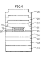
reference numeral 74 indicates a plate line. - Figure 6 shows an example arrangement of the
bit line 72 and theword line 73. - In Figure 6, by forming the
bit line 72 and theword line 73 in a spacing at the central portion between theferromagnetic layer 34 and the antiferromagnetic layer (closed magnetic circuit layer) 36, a current value required for inverting the magnetization directions of theferromagnetic layer 34 and the ferromagnetic layer (closed magnetic circuit layer) 36 can be reduced, thereby suppressing power consumption of the magnetic memory. - Both the
bit line 72 and theword line 73 are electrically insulated from theferromagnetic layer 34 and the ferromagnetic layer (closed magnetic circuit layer) 36. - The following descriptions will discuss still another embodiment of the present invention in reference to figures.
- Figure 7 shows a schematic structure of an MTJ device of the present embodiment.
- As shown in Figure 7, the MTJ device 4 in accordance with the present embodiment includes an antiferromagnetic layer 41 (first antiferromagnetic layer), a ferromagnetic layer 42 (first magnetic layer), an insulating layer 43 (first insulating layer), a ferromagnetic layer 44 (second magnetic layer), metal layers 45, 45', a ferromagnetic layer (closed magnetic circuit layer, fourth magnetic layer) 46, an insulating layer 47 (second insulating layer), a ferromagnetic layer 48 (third magnetic layer) and an antiferromagnetic layer 49 (second antiferromagnetic layer). The
ferromagnetic layer 44 and the antiferromagnetic layer (closed magnetic circuit layer) 46 are connected via the metal layers 45, 45' at both end parts with a spacing at a central portion. - In the above arrangement, by setting the film thickness of the metal layers 45, 45' such that an antiferromagnetic coupling is exerted between the
ferromagnetic layer 44 and the ferromagnetic layer (closed magnetic circuit layer) 46, the respective magnetization directions of theantiferromagnetic layer 44 and the ferromagnetic layer (closed magnetic circuit layer) 46 can be made opposite to each other. Therefore, the respective magnetization of theferromagnetic layer 44 and the ferromagnetic layer (closed magnetic circuit layer) 46 form a closed loop, and thus generation of a magnetic wall at both end parts of theferromagnetic layer 44 can be avoided. - The MTJ device 4 of the present embodiment differs from the
MTJ device 3 of the second embodiment in that theferromagnetic layer 42 is composed of twoferromagnetic layer 42a (second ferromagnetic layer) and theferromagnetic layer 42c which are antiferromagnetically coupled via ametal layer 42b (second metal layer), and theferromagnetic layer 42c (first ferromagnetic layer) which is exchange coupled with the antiferromagnetic layer 41. As in the second embodiment, theantiferromagnetic layer 49 and theferromagnetic layer 48 are exchange coupled. - The magnetization of the
ferromagnetic layer 48 is fixed by exchange coupling with theantiferromagnetic layer 49. The magnetization of theantiferromagnetic layer 42c is fixed by exchange coupling with the antiferromagnetic layer 41. Further, theferromagnetic layer 42a is antiferromagnetically coupled via theantiferromagnetic layer 42b, and thus has magnetization in opposite direction to theantiferromagnetic layer 42c. - The MTJ device 4 records information based on the magnetization direction of a closed loop composed of the
antiferromagnetic layer 44 and the antiferromagnetic layer (closed magnetic circuit layer) 46. The MTJ device 4 reads out information based on changes in resistance depending on whether the magnetization direction of the closed loop composed of theferromagnetic layer 44 and the antiferromagnetic layer (closed magnetic circuit layer) 46 and the magnetization direction of theferromagnetic layers - As described, in order to read out information in the foregoing manner, i.e., based on changes in resistance depending on whether the magnetization direction of the closed loop composed of the
ferromagnetic layer 44 and the antiferromagnetic layer (closed magnetic circuit layer) 46 and the magnetization direction of theferromagnetic layers ferromagnetic layer 42c in the same direction as theantiferromagnetic layer 48. - According to the foregoing arrangement, the respective magnetizations of the
ferromagnetic layer 42c and theferromagnetic layer 48 can be fixed with a single treatment or a magnetic field of the same direction. As a result, the process of reading out can be simplified as compared to the previous embodiment. - In the present embodiment, the
ferromagnetic layer 42 of a double layer structure, and anferromagnetic layer 48 of a single layer structure are adopted. However, the present invention is not limited to this arrangement as long as the condition that the respective numbers of magnetic layers differ between the two fixed layers by one. - In the present embodiment, the same antiferromagnetic material may be used for the antiferromagnetic layer 41 and the
antiferromagnetic layer 49. - The MTJ device 4 of the present embodiment can be used in the magnetic memory as in the
MTJ device 3 of the second embodiment. - In the present embodiment, only the MTJ device portion is shown; however, it is needless to mention that in actual device forming process, the electrode for supplying current, the substrate, the protective layer and an adhesive layer are needed.
- The following descriptions will discuss still another embodiment of the present invention in reference to figures.
- A magnetic memory adopting an MTJ device in accordance with the present embodiment is shown in Figure 8. As shown in Figure 8, respective
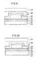
magnetic memory cells 51 are disposed at intersections between a bit lines 52 (first current line) and the word lines 53 (second current lines). Themagnetic memory cell 51 has the closed magnetic circuit structure in the vertical axis direction in the Figure, and has the magnetization also in the vertical axis direction. Figure 9 shows a cross section cut by a line A-B of Figure 8. For simplification, a single magnetic memory cell is shown. - As shown in Figure 9, the
magnetic memory cell 51 includes a closedmagnetic circuit layer 65 formed on the MTJ device composed of anantiferromagnetic layer 61, anferromagnetic layer 62, an insulatinglayer 63, and a ferromagnetic layer 64 (magnetic layer). Theantiferromagnetic layer 61 and theantiferromagnetic layer 62 are exchange coupled. Theferromagnetic layer 64 and the closedmagnetic circuit layer 65 are connected at both end portions, and are separated at the central portion. Thebit line 52 is provided in the above spacing in the central portion, and is electrically connected to the MTJ device. Theword line 53 is provided on themagnetic memory cell 51 via the insulatinglayer 66. - Therefore, one end of the MTJ device is electrically connected to the
bit line 52, and the other end is connected to a drain of the selective transistor (not shown). The word line is electrically insulated from the MTJ device and is connected to a gate of a selective transistor (not shown). As a result, randomly accessible layout shown in Figure 5 can be realized. - The information of the magnetic memory cell are recorded in the magnetization direction of the
ferromagnetic layer 64. On the other hand, the magnetization direction of theferromagnetic layer 62 is fixed by an exchange coupling with theantiferromagnetic layer 61. Therefore, the information recorded in the magnetic memory cell, i.e., the magnetization direction of the ferromagnetic layer is detected based on changes in resistance whether the respective magnetization directions of theferromagnetic layer 62 and theantiferromagnetic layer 64 are in parallel or in antiparallel. - The rewriting of information on the magnetic memory cell can be realized by changing the magnetization direction of the
ferromagnetic layer 64 by applying current to thebit line 52 and theword line 53. In this state, except for themagnetic memory cell 51 disposed at the intersection between thebit line 52 for flowing therethrough current and theword line 53, the magnetization of theferromagnetic layer 62 of the magnetic memory cell is needed to be fixed. This condition can be realized, for example, as below-indicated. - The
ferromagnetic layer 64 can store information, and has coercive force that enables rewriting at a recording current. On the other hand, the closedmagnetic circuit layer 65 is made of a material having a smaller coercive force than that of theferromagnetic layer 64. When rewriting information in themagnetic memory cell 51, such current that inverts magnetization of the closedmagnetic circuit layer 65 but the magnetization of theferromagnetic layer 64 is not inverted is applied to thebit line 52. To theword line 53, such current that the synthetic magnetic field with thebit line 52 inverts the magnetization of theferromagnetic layer 64, but the magnetization of theferromagnetic layer 64 is not inverted by theword line 53 alone. In this state, the magnetic field from thebit line 52 is not applied to other cells than themagnetic memory cell 51 on thebit line 52, and thus, the magnetization direction of theferromagnetic layer 42 is not changed. - As described, by controlling the magnetic characteristics of the
ferromagnetic layer 64 and the closedmagnetic circuit layer 65 and the level of current applied to thebit line 52 and theword line 53, only the magnetization direction of themagnetic memory cell 51 at the intersection between thebit line 52 and theword line 53 can be changed. - According to the described arrangement, the
bit line 52 is provided in the closed magnetic circuit structure composed of theferromagnetic layer 64 and the closedmagnetic circuit layer 65, the magnetization of the closedmagnetic circuit layer 65 is inverted at sufficiently low current, and a magnetic field can be effectively applied to theferromagnetic layer 64. Therefore, compared to the conventional structure shown in Figure 4, the magnetization direction of themagnetic memory cell 51 can be altered at sufficiently low current. Therefore, by constituting the closedmagnetic circuit layer 65 of a material of high permeability, it is effective to reduce the recording current. - Another example of the
magnetic memory cell 51 shown in Figure 8 is shown in Figure 10. The structure shown in Figure 9 differs from the structure shown in Figure 8 in that theferromagnetic layer 64 and the closedmagnetic circuit layer 65 are connected via themetal layer 67. The thickness of themetal layer 67 is set such that theferromagnetic layer 64 and the closedmagnetic circuit layer 65 are exchange coupled. Therefore, when carrying out the rewriting of information on themagnetic memory cell 51 in the above manner, in other magnetic memory cells than themagnetic cell 51, in which rewriting of information is not performed, the respective magnetizations of theferromagnetic layer 64 and the closedmagnetic circuit layer 65 surely form a closed magnetic circuit by the antiferromagnetic coupling via themetal layer 67. - In the present embodiment, as a magnetic memory cell having a closed magnetic circuit structure, two examples adopting the MTJ device have been shown; however, the present invention is not limited to the above, and the magnetic memory cell having other closed magnetic circuit structure may be adopted. In the present embodiment, the word line is provided on the bit line, however, it may be provided below the MTJ device. Also, it may be arranged so as to insulate the bit line from the MTJ device, or the bit line and the word line are exchanged, or the bit line or the word line are separately provided for recording and reading out. The bit line, word line, and the closed magnetic circuit structure are not limited to the above.
- As described, the first magnetic tunnel junction device of the present invention including at least a first magnetic layer, an insulating layer and a second magnetic layer which are laminated in this order, is characterized by further including: a third magnetic layer formed on an opposite side of an insulating layer forming side of the first or second magnetic layer via a metal layer with a spacing formed at a central portion, wherein the first or second magnetic layer and the third magnetic layer form a closed magnetic circuit.
- According to the forgoing arrangement, the magnetization of the third magnetic layer serving as the closed magnetic circuit layer and the first or second magnetic layer form a closed loop; and thus the generation of the magnetic poles at both end portions can be avoided. As described, according to the MTJ device of the described structure, effects of the magnetic poles generated at both end portions can be avoided. Thus, a stable magnetization state as recorded can be maintained even for a miniaturized pattern. Additionally, since the memory layer of the ferromagnetic layer has a closed magnetic circuit structure, stable magnetization state as recorded can be ensured against an external leakage magnetic field.
- The second magnetic tunnel junction device having the structure of the first magnetic tunnel junction device is characterized in that at least one lead line is formed in the spacing between the third magnetic layer and the first or second magnetic layer.
- According to the foregoing structure, by forming the lead line in the spacing at the central portion between the first or second magnetic layer and the third magnetic layer, a current value required for inverting the magnetization direction of the magnetic layer and the closed magnetic circuit layer can be reduced, and the power consumption of the magnetic memory adopting the MTJ device can be reduced.
- The third magnetic tunnel junction device of the present invention which includes at least the first magnetic layer, the first insulating layer, the second magnetic layer, the second insulating layer and the third magnetic layer which are laminated is characterized by including:
a fourth magnetic layer formed on a first insulating layer laminating side or a second insulating layer laminating side of the second magnetic layer via a metal layer with a spacing at a central portion, and the second magnetic layer and the fourth magnetic layer form a closed magnetic circuit. - According to the described arrangement, a high resistance change ratio can be obtained, and the effects of the magnetic poles generated at both end portions can be reduced. Thus, a stable magnetization state as recorded can be maintained even for a miniaturized pattern. Additionally, since the memory layer of the ferromagnetic layer has a closed magnetic circuit structure, stable magnetization state as recorded can be ensured against an external leakage magnetic field.
- The fourth magnetic tunnel junction device of the present invention having the structure of the third magnetic tunnel junction device is characterized by further including a first antiferromagnetic layer which is exchange-coupled with the first magnetic layer, and a second antiferromagnetic layer which is exchange coupled with the third magnetic layer.
- The fifth magnetic tunnel junction device of the present invention having the structure of the fourth magnetic tunnel junction device is characterized in that an exchange coupling between the first antiferromagnetic layer and the first magnetic layer disappears at different temperature from a temperature at which an exchange coupling between the second antiferromagnetic layer and the third magnetic layer disappears.
- The sixth magnetic tunnel junction device having the structure of the first or second magnetic tunnel junction device is characterized in that:
at least the first magnetic layer or the second magnetic layer is composed of two or more ferromagnetic layers which are antiferromagnetically coupled via a metal layer. - According to the above arrangement, in order to read out information in the foregoing manner, i.e., based on changes in resistance depending on whether the magnetization direction of the closed loop composed of the first or third magnetic layer and the second magnetic layer (closed magnetic circuit layer), and the magnetization direction of the ferromagnetic layer and the first or third magnetic layer are parallel to or antiparallel to one another, it is required to fix the magnetization direction of the ferromagnetic layer in the same direction as the first or third magnetic layer.
- According to the above arrangement, the magnetization direction of the ferromagnetic layer and the first or third magnetic layer can be fixed with a single treatment or a magnetic field of the same direction. As a result, the process of reading out can be simplified.
- With the foregoing preferred embodiment, the first magnetic layer composed of two ferromagnetic layers, and the third magnetic layer of a single ferromagnetic layer are adopted. However, the present invention is not limited to this arrangement as long as the condition that the respective numbers of magnetic layers differ between the two fixed layers by one.
- In the present embodiment, the same antiferromagnetic material may be used for the antiferromagnetic layer 41 and the
antiferromagnetic layer 49. - The seventh magnetic tunnel junction device of the present invention having any of the third through sixth magnetic tunnel junction devices, is characterized in that:
at least one lead line is formed in the spacing between the second magnetic layer and the fourth magnetic layer. - According to the described arrangement, by forming the lead line in the spacing between the second magnetic layer and the fourth magnetic layer, a current value required for inverting the magnetization direction of the second magnetic layer and the fourth magnetic layer (closed magnetic circuit layer) can be reduced.
- The first magnetic memory of the present invention is characterized by adopting a magnetic tunnel junction device of the present invention which includes at least a first magnetic layer, an insulating layer and a second magnetic layer which are laminated in this order and further includes a third magnetic layer serving as a closed magnetic circuit layer formed on different side of an insulating layer forming side of the first magnetic layer or the second magnetic layer, wherein the third magnetic layer is formed via a metal layer so as to have a spacing at a central portion, and the third magnetic layer forms a closed magnetic circuit with the first magnetic layer or the second magnetic layer.
- According to the forgoing arrangement, the magnetization of the third magnetic layer serving as the closed magnetic circuit layer and the first or second magnetic layer form a closed loop; and thus the generation of the magnetic poles at both end portions can be avoided. As described, according to the MTJ device of the described structure, effects of the magnetic poles generated at both end portions can be eliminated. Thus, a stable magnetization state as recorded can be maintained for a miniaturized pattern. Additionally, since the memory layer of the ferromagnetic layer has a closed magnetic circuit structure, a stable magnetization state as recorded can be ensured against an external leakage magnetic field. Therefore, a power consumption of the magnetic memory adopting the MTJ device can be reduced.
- The second magnetic memory of the present invention having the structure of the first magnetic memory is characterized by including at least one lead line in the spacing between the first or second magnetic layer and the third magnetic layer.
- The third magnetic memory of the present invention is characterized by including a magnetic tunnel junction device which includes at least the first magnetic layer, the first insulating layer, the second magnetic layer, the second insulating layer and the third magnetic layer which are laminated, and further includes a fourth magnetic layer formed on a first insulating layer laminating side or a second insulating layer laminating side of the second magnetic layer via a metal layer with a spacing at a central portion, wherein the second magnetic layer and the fourth magnetic layer forms a closed magnetic circuit.
- According to the described arrangement, a high resistance change ratio is obtained, and the effects of the magnetic poles generated at the end portion can be reduced. Thus, a stable magnetization state as recorded can be maintained for a miniaturized pattern. As a result, a magnetic memory of an improved integration can be realized, and a power consumption of the magnetic memory can be reduced.
- The access method of the magnetic memory cell of the present invention is characterized by including the steps of:
- forming a closed magnetic circuit on a magnetic layer for storing a memory of a magnetic memory cell;
- placing a first current line in a closed magnetic circuit composed of the magnetic layer and the closed magnetic circuit layer, and a second current line outside the closed magnetic circuit;
- changing the magnetization direction of the magnetic layer by applying such current to the first current line that the magnetization of the closed magnetic circuit layer is inverted but the magnetization of the magnetic layer is not inverted, and applying such current to the second current line that the magnetization of the magnetic layer is not inverted by the second current line alone, but the magnetization of the magnetic layer is inverted by a synthetic magnetic field with the first current line.
-
- According to the described access method of the magnetic memory cell, by controlling the magnetic characteristics of the ferromagnetic layer and the closed magnetic circuit layer and the level of current flowing through the first current line (bit line) and the second current line (word line), access to only one magnetic memory cell is permitted, and a required recording current can be reduced. Further, the effects of magnetic poles at both end portions on the magnetic memory cell can be suppressed. As a result, a stable magnetization state can be ensured even for a miniaturized pattern, and a highly integrated magnetic memory can be realized. Additionally, by adopting the closed magnetic circuit layer structure for the memory layer, a stable magnetization state as recorded can be ensured against an external leakage magnetic field. Further, a power consumption of the magnetic memory can be reduced.
- Further, the first current line is formed within the closed magnetic circuit layer structure formed by the magnetic layer (ferromagnetic layer 64) and the closed magnetic circuit layer, the magnetization of the closed magnetic circuit layer can be inverted at sufficiently low current, thereby effectively applying the magnetic layer.
- The first magnetic cell of the present invention adopting the above access method is characterized by including a magnetic tunnel junction device which includes a first magnetic layer, an insulating layer, and a second magnetic layer which are laminated in this order, wherein at least the closed magnetic circuit layer is formed on an opposite side of an insulating layer forming side of the first or second magnetic layer with a spacing at a central portion, and the first or second magnetic layer and the closed magnetic circuit layer form a closed magnetic circuit.
- The second magnetic cell of the present invention adopting the above access method is characterized by including a magnetic tunnel junction device which includes a first magnetic layer, an insulating layer, and a second magnetic layer which are laminated in this order, wherein at least the closed magnetic circuit layer is formed on an opposite side of an insulating layer forming side of the first or second magnetic layer via a metal layer with a spacing at a central portion, and the first or second magnetic layer and the closed magnetic circuit layer form a closed magnetic circuit.
- The invention being thus described, it will be obvious that the same may be varied in many ways. Such variations are not to be regarded as a departure from the spirit and scope of the invention, and all such modification as would be obvious to one skilled in the art are intended to be included within the scope of the following claims.
Claims (23)
- A magnetic tunnel junction device comprising at least a first magnetic layer, an insulating layer and a second magnetic layer which are laminated in this order, characterized by further comprising:a third magnetic layer (17) formed on an opposite side of an insulating layer forming side of said first or second magnetic layer via a metal layer with a spacing formed at a central portion,wherein said first or second magnetic layer and said third magnetic layer form a closed magnetic circuit.
- The magnetic tunnel junction device as set forth in claim 1, characterized in that:
at least one lead line is formed in said spacing between said first or second magnetic layer and said third magnetic layer. - The magnetic tunnel junction device as set forth in claim 1, characterized in that:
a thickness of the metal film is set to such thickness that said first or second magnetic layer and the third magnetic layer are antiferromagnetically coupled. - The magnetic tunnel junction device as set forth in any one of claims 1 through 3, characterized in that:
said metal layer is formed on both end portions. - The magnetic tunnel junction device as set forth in any one of claims 1 through 4, characterized in that:
said metal film is made of a material selected from the group consisting of Ru, Cr, Cu and alloys thereof. - A magnetic memory adopting a magnetic tunnel junction device, characterized by comprising at least a first magnetic layer, an insulating layer and a second magnetic layer which are laminated in this order, and a third magnetic layer formed on an opposite side of an insulating layer forming side of the first or second magnetic layer via a metal layer with a spacing at a central portion, wherein said first or second magnetic layer and said third magnetic layer form a closed magnetic circuit.
- The magnetic memory as set forth in claim 6, characterized in that at least a lead line is formed in a spacing between said first or second magnetic layer and said third magnetic layer.
- A magnetic tunnel junction device comprising a first magnetic layer, a first insulating layer, a second magnetic layer, a second insulating layer and a third magnetic layer which are laminated, characterized by further comprising:a fourth magnetic layer (36) formed on either a first insulating layer forming side or a second insulating layer forming side of said second magnetic layer via a metal layer with a spacing at a central portion,wherein said second magnetic layer and said fourth magnetic layer form a closed magnetic circuit.
- The magnetic tunnel junction device as set forth in claim 8, characterized by further comprising:a first antiferromagnetic layer (31) which is exchange coupled with the first magnetic layer, anda second antiferromagnetic layer (36) which is exchange coupled with the third magnetic layer.
- The magnetic tunnel junction device as set forth in claim 9, characterized in that:
an exchange coupling between said first antiferromagnetic layer and the first magnetic layer disappears at different temperature from a temperature at which an exchange coupling between said second antiferromagnetic layer and said third magnetic layer disappears. - The magnetic tunnel junction device as set forth in any one of claim 9 or 10, characterized in that:
at least either the first magnetic layer (42) or the third magnetic layer (48) is constituted by at least two ferromagnetic layers (42a, 42c) which are antiferromagnetically coupled via a second metal layer (42b). - The magnetic tunnel junction device as set forth in any one of claims 8 through 11, characterized in that:
at least one lead line is formed in a spacing between the second magnetic layer and the fourth magnetic layer. - The magnetic tunnel junction device as set forth in any one of claims 8 through 12, characterized in that:
a film thickness of said metal layer is adjusted such that said second magnetic layer and said fourth magnetic layer are antiferromagnetically coupled. - The magnetic tunnel junction device, as set forth in any one of claims 9 through 13, characterized in that:
respective magnetizations of said first magnetic layer and said first antiferromagentic layer, and respective magnetizations of said third magnetic layer and said second antiferromagnetic layer are exchange coupled, which are fixed in opposite directions. - The magnetic tunnel junction device, as set forth in any one of claims 9 through 14, characterized in that:
respective number of magnetic layers of said first magnetic layer and said third magnetic layer differ by one. - The magnetic tunnel junction device set forth in claim 15, characterized in that:said third magnetic layer is a single layer, andsaid first magnetic layer includes a first ferromagnetic layer and a third ferromagnetic layer which are antiferromagnetically coupled via a second metal layer, anda magnetization direction of said first ferromagnetic layer is fixed in a magnetization direction of said third magnetic layer.
- The magnetic tunnel junction device as set forth in any one of claims 8 through 16, characterized in that:
said metal film is made of a material selected from the group consisting of Ru, Cr, Cu and alloys thereof. - A magnetic memory characterized by adopting a magnetic tunnel junction device which comprises a first magnetic layer, a first insulating layer, a second insulating layer and a third insulating layer which are laminated, and further comprises a fourth magnetic layer formed either a first insulating layer forming side or a second insulating layer forming side of said second magnetic layer via a metal layer with a spacing formed at a central portion,
wherein said second magnetic layer and the fourth magnetic layer form a closed magnetic circuit. - An access method of a magnetic memory cell characterized by comprising the steps of:forming a closed magnetic circuit on a magnetic layer for storing a memory of a magnetic memory cell;placing a first current line (52) in a closed magnetic circuit composed of the magnetic layer and the closed magnetic circuit layer, and a second current line (53) outside the closed magnetic circuit;changing the magnetization direction of the magnetic layer by applying such current to the first current line that the magnetization of the closed magnetic circuit layer is inverted but the magnetization of the magnetic layer is not inverted, and applying such current to the second current line that the magnetization of the magnetic layer is not inverted by the second current line alone, but the magnetization of the magnetic layer is inverted by a synthetic magnetic field with the first current line.
- A magnetic memory cell adopting an access method which comprises the steps of:forming a closed magnetic circuit on a magnetic layer for storing a memory of a magnetic memory cell; placing a first current line in a closed magnetic circuit composed of the magnetic layer and the closed magnetic circuit layer, and a second current line outside the closed magnetic circuit; and changing the magnetization direction of the magnetic layer by applying such current to the first current line that the magnetization of the closed magnetic circuit layer is inverted but the magnetization of the magnetic layer is not inverted, and applying such current to the second current line that the magnetization of the magnetic layer is not inverted by the second current line alone, but the magnetization of the magnetic layer is inverted by a synthetic magnetic field with the first current line,said magnetic memory cell, characterized by comprising a magnetic tunnel junction device which includes a first magnetic layer, an insulating layer, and a second magnetic layer which are laminated in this order, wherein at least the closed magnetic circuit layer is formed on an opposite side of an insulating layer forming side of said first or second magnetic layer with a spacing at a central portion, andthe first or second magnetic layer and the closed magnetic circuit layer form a closed magnetic circuit.
- The magnetic memory cell a set forth in claim 20, characterized in that:
said closed magnetic circuit layer is made of a material of a small coercive force than the first or second magnetic layer which forms a closed magnetic circuit with the closed magnetic circuit layer. - A magnetic memory cell adopting an access method, characterized by comprising the steps of:forming a closed magnetic circuit on a magnetic layer for storing a memory of a magnetic memory cell; placing a first current line in a closed magnetic circuit composed of the magnetic layer and the closed magnetic circuit layer, and a second current line outside the closed magnetic circuit; and changing the magnetization direction of the magnetic layer by applying such current to the first current line that the magnetization of the closed magnetic circuit layer is inverted but the magnetization of the magnetic layer is not inverted, and applying such current to the second current line that the magnetization of the magnetic layer is not inverted by the second current line alone, but the magnetization of the magnetic layer is inverted by a synthetic magnetic field with the first current line,said magnetic memory cell, characterized by comprising a magnetic tunnel junction device which includes a first magnetic layer, an insulating layer, and a second magnetic layer which are laminated in this order, wherein at least the closed magnetic circuit layer is formed on an opposite side of an insulating layer forming side of said first or second magnetic layer via a metal layer with a spacing at a central portion, andthe first or second magnetic layer and the closed magnetic circuit layer form a closed magnetic circuit.
- The magnetic memory cell as set forth in claim 22, characterized in that:
a film thickness of said metal layer is adjusted such that the closed magnetic circuit layer and the first or second magnetic layer which forms a closed magnetic circuit with the closed magnetic circuit layer are ferromagnetically coupled.
Applications Claiming Priority (6)
| Application Number | Priority Date | Filing Date | Title |
|---|---|---|---|
| JP35104899 | 1999-12-10 | ||
| JP35104899 | 1999-12-10 | ||
| JP2000045447 | 2000-02-23 | ||
| JP2000045447A JP2001237470A (en) | 2000-02-23 | 2000-02-23 | Magnetic tunnel junction element and magnetic memory using the same |
| JP2000065913 | 2000-03-10 | ||
| JP2000065913A JP3738165B2 (en) | 2000-03-10 | 2000-03-10 | Magnetic memory cell |
Publications (3)
| Publication Number | Publication Date |
|---|---|
| EP1107329A2 true EP1107329A2 (en) | 2001-06-13 |
| EP1107329A3 EP1107329A3 (en) | 2002-01-16 |
| EP1107329B1 EP1107329B1 (en) | 2011-07-06 |
Family
ID=27341361
Family Applications (1)
| Application Number | Title | Priority Date | Filing Date |
|---|---|---|---|
| EP00126994A Expired - Lifetime EP1107329B1 (en) | 1999-12-10 | 2000-12-08 | Magnetic tunnel junction device, magnetic memory adopting the same, magnetic memory cell and access method of the same |
Country Status (3)
| Country | Link |
|---|---|
| US (1) | US6519179B2 (en) |
| EP (1) | EP1107329B1 (en) |
| CN (1) | CN1193441C (en) |
Cited By (5)
| Publication number | Priority date | Publication date | Assignee | Title |
|---|---|---|---|---|
| WO2003056562A1 (en) * | 2001-12-21 | 2003-07-10 | Motorola, Inc. | Magneto-electronic component for high density memory |
| EP1335382A1 (en) * | 2002-01-31 | 2003-08-13 | Sharp Kabushiki Kaisha | Magnetic yoke structure in MRAM devices to reduce programming power consumption and a method to make the same |
| EP1398790A2 (en) * | 2002-09-13 | 2004-03-17 | TDK Corporation | Magnetoresistive effect element, magnetic memory device and method of fabricating the same |
| EP1406266A2 (en) * | 2002-09-25 | 2004-04-07 | TDK Corporation | Magnetic memory and its write/read method |
| EP1505606A2 (en) * | 2003-07-25 | 2005-02-09 | TDK Corporation | Magnetic storage cell and magnetic memory device using same |
Families Citing this family (15)
| Publication number | Priority date | Publication date | Assignee | Title |
|---|---|---|---|---|
| US6724674B2 (en) * | 2000-11-08 | 2004-04-20 | International Business Machines Corporation | Memory storage device with heating element |
| JP5019681B2 (en) * | 2001-04-26 | 2012-09-05 | ルネサスエレクトロニクス株式会社 | Thin film magnetic memory device |
| US6750491B2 (en) * | 2001-12-20 | 2004-06-15 | Hewlett-Packard Development Company, L.P. | Magnetic memory device having soft reference layer |
| CN100547678C (en) * | 2002-12-18 | 2009-10-07 | Nxp股份有限公司 | The HSD and the method that are used for magnetic memory cell |
| JP4365591B2 (en) * | 2003-01-17 | 2009-11-18 | Tdk株式会社 | Magnetic memory device, write current drive circuit, and write current drive method |
| US6756239B1 (en) * | 2003-04-15 | 2004-06-29 | Hewlett-Packard Development Company, L.P. | Method for constructing a magneto-resistive element |
| FR2860910B1 (en) * | 2003-10-10 | 2006-02-10 | Commissariat Energie Atomique | MAGNETIC TUNNEL JUNCTION DEVICE AND METHOD OF WRITING / READING SUCH A DEVICE |
| US20060281258A1 (en) * | 2004-10-06 | 2006-12-14 | Bernard Dieny | Magnetic tunnel junction device and writing/reading method for said device |
| US20050110004A1 (en) * | 2003-11-24 | 2005-05-26 | International Business Machines Corporation | Magnetic tunnel junction with improved tunneling magneto-resistance |
| US7221584B2 (en) * | 2004-08-13 | 2007-05-22 | Taiwan Semiconductor Manufacturing Company, Ltd. | MRAM cell having shared configuration |
| KR100707170B1 (en) * | 2004-08-23 | 2007-04-13 | 삼성전자주식회사 | Magnetic memory device having uniform switching characteristics and capable of switching with low current and method of operating the same |
| JP2007059865A (en) * | 2005-07-27 | 2007-03-08 | Tdk Corp | Magnetic storage |
| KR100655438B1 (en) * | 2005-08-25 | 2006-12-08 | 삼성전자주식회사 | Magnetic memory device and method of forming the same |
| JPWO2007043358A1 (en) * | 2005-10-07 | 2009-04-16 | コニカミノルタオプト株式会社 | Method for producing cellulose ester film, cellulose ester film, polarizing plate and liquid crystal display device |
| US7547480B2 (en) * | 2005-10-28 | 2009-06-16 | Everspin Technologies, Inc. | Magnetic tunnel junction pressure sensors and methods |
Citations (3)
| Publication number | Priority date | Publication date | Assignee | Title |
|---|---|---|---|---|
| US4455626A (en) | 1983-03-21 | 1984-06-19 | Honeywell Inc. | Thin film memory with magnetoresistive read-out |
| US5587943A (en) | 1995-02-13 | 1996-12-24 | Integrated Microtransducer Electronics Corporation | Nonvolatile magnetoresistive memory with fully closed flux operation |
| JPH09106514A (en) | 1995-10-06 | 1997-04-22 | Fujitsu Ltd | Ferromagnetic tunnel element and its production |
Family Cites Families (7)
| Publication number | Priority date | Publication date | Assignee | Title |
|---|---|---|---|---|
| US6256222B1 (en) * | 1994-05-02 | 2001-07-03 | Matsushita Electric Industrial Co., Ltd. | Magnetoresistance effect device, and magnetoresistaance effect type head, memory device, and amplifying device using the same |
| US5650958A (en) | 1996-03-18 | 1997-07-22 | International Business Machines Corporation | Magnetic tunnel junctions with controlled magnetic response |
| JP4054403B2 (en) | 1997-04-28 | 2008-02-27 | キヤノン株式会社 | Magnetic thin film memory |
| JP4136028B2 (en) | 1997-04-28 | 2008-08-20 | キヤノン株式会社 | Magnetic thin film memory element, magnetic thin film memory using the same, and recording / reproducing method thereof |
| DE69835475D1 (en) * | 1997-04-28 | 2006-09-21 | Canon Kk | Magnetic thin film memory element using the GMR effect and magnetic thin film memory |
| JPH11163436A (en) | 1997-11-27 | 1999-06-18 | Matsushita Electric Ind Co Ltd | Magnetoresistance effect element and magnetoresistance effect type head |
| DE19836567C2 (en) * | 1998-08-12 | 2000-12-07 | Siemens Ag | Memory cell arrangement with memory elements with a magnetoresistive effect and method for their production |
-
2000
- 2000-12-08 EP EP00126994A patent/EP1107329B1/en not_active Expired - Lifetime
- 2000-12-08 US US09/733,646 patent/US6519179B2/en not_active Expired - Fee Related
- 2000-12-09 CN CNB001310593A patent/CN1193441C/en not_active Expired - Fee Related
Patent Citations (3)
| Publication number | Priority date | Publication date | Assignee | Title |
|---|---|---|---|---|
| US4455626A (en) | 1983-03-21 | 1984-06-19 | Honeywell Inc. | Thin film memory with magnetoresistive read-out |
| US5587943A (en) | 1995-02-13 | 1996-12-24 | Integrated Microtransducer Electronics Corporation | Nonvolatile magnetoresistive memory with fully closed flux operation |
| JPH09106514A (en) | 1995-10-06 | 1997-04-22 | Fujitsu Ltd | Ferromagnetic tunnel element and its production |
Cited By (11)
| Publication number | Priority date | Publication date | Assignee | Title |
|---|---|---|---|---|
| WO2003056562A1 (en) * | 2001-12-21 | 2003-07-10 | Motorola, Inc. | Magneto-electronic component for high density memory |
| EP1335382A1 (en) * | 2002-01-31 | 2003-08-13 | Sharp Kabushiki Kaisha | Magnetic yoke structure in MRAM devices to reduce programming power consumption and a method to make the same |
| EP1398790A2 (en) * | 2002-09-13 | 2004-03-17 | TDK Corporation | Magnetoresistive effect element, magnetic memory device and method of fabricating the same |
| EP1398790A3 (en) * | 2002-09-13 | 2005-01-12 | TDK Corporation | Magnetoresistive effect element, magnetic memory device and method of fabricating the same |
| US7016221B2 (en) | 2002-09-13 | 2006-03-21 | Tdk Corporation | Magnetoresistive effect element, magnetic memory device and method of fabricating the same |
| EP1406266A2 (en) * | 2002-09-25 | 2004-04-07 | TDK Corporation | Magnetic memory and its write/read method |
| EP1406266A3 (en) * | 2002-09-25 | 2004-10-20 | TDK Corporation | Magnetic memory and its write/read method |
| US6930911B2 (en) | 2002-09-25 | 2005-08-16 | Tdk Corporation | Magnetic memory device, method for writing on the same and method for reading from the same |
| EP1505606A2 (en) * | 2003-07-25 | 2005-02-09 | TDK Corporation | Magnetic storage cell and magnetic memory device using same |
| EP1505606A3 (en) * | 2003-07-25 | 2005-09-21 | TDK Corporation | Magnetic storage cell and magnetic memory device using same |
| US7035139B2 (en) | 2003-07-25 | 2006-04-25 | Tdk Corporation | Magnetic storage cell and magnetic memory device using same |
Also Published As
| Publication number | Publication date |
|---|---|
| EP1107329A3 (en) | 2002-01-16 |
| EP1107329B1 (en) | 2011-07-06 |
| CN1193441C (en) | 2005-03-16 |
| US20010005011A1 (en) | 2001-06-28 |
| US6519179B2 (en) | 2003-02-11 |
| CN1305234A (en) | 2001-07-25 |
Similar Documents
| Publication | Publication Date | Title |
|---|---|---|
| US6519179B2 (en) | Magnetic tunnel junction device, magnetic memory adopting the same, magnetic memory cell and access method of the same | |
| US6396735B2 (en) | Magnetic memory element, magnetic memory and manufacturing method of magnetic memory | |
| US7018725B2 (en) | Magneto-resistance effect element magneto-resistance effect memory cell, MRAM, and method for performing information write to or read from the magneto-resistance effect memory cell | |
| US7245464B2 (en) | Magnetic memory having a ferromagnetic tunneling junction | |
| US6127045A (en) | Magnetic tunnel junction device with optimized ferromagnetic layer | |
| US7190613B2 (en) | Magnetic random access memory device having thermal agitation property and high write efficiency | |
| KR100421408B1 (en) | Magnetoresistive element and magnetic memory device | |
| US8492881B2 (en) | Magnetic storage device | |
| US6628542B2 (en) | Magnetoresistive device and magnetic memory using the same | |
| US6906898B2 (en) | Differential detection read sensor, thin film head for perpendicular magnetic recording and perpendicular magnetic recording apparatus | |
| JP4076197B2 (en) | Magnetic element, storage device, magnetic reproducing head, three-terminal element, and magnetic disk device | |
| JP3977576B2 (en) | Magnetic memory device | |
| US6542343B1 (en) | Tunnel valve head design to lower resistance | |
| JP3634761B2 (en) | Magnetoresistive element, memory element using the magnetoresistive element, magnetic random access memory, and recording / reproducing method | |
| US20070133264A1 (en) | Storage element and memory | |
| KR19990062685A (en) | Magnetoresistive effect element and manufacturing method thereof | |
| US6442064B1 (en) | Magnetic tunnel junction element and magnetic memory using the same | |
| JP2001217479A (en) | Magnetic tunnel junction element and magnetic memory using the same | |
| JP3658331B2 (en) | Recording / reproducing method of memory element, magnetoresistive element, and magnetic random access memory | |
| JP3515940B2 (en) | Magnetic tunnel junction device and magnetic memory using the same | |
| JP3738165B2 (en) | Magnetic memory cell | |
| JP2001230468A (en) | Magnetic tunnel junction element and magnetic memory using the same | |
| JP2002353418A (en) | Magnetoresistive effect element and magnetic memory device | |
| JP3625424B2 (en) | Magnetic tunnel junction device and magnetic memory using the same | |
| JP2002217382A (en) | Magnetic memory and method for manufacturing the same |
Legal Events
| Date | Code | Title | Description |
|---|---|---|---|
| PUAI | Public reference made under article 153(3) epc to a published international application that has entered the european phase |
Free format text: ORIGINAL CODE: 0009012 |
|
| AK | Designated contracting states |
Kind code of ref document: A2 Designated state(s): AT BE CH CY DE DK ES FI FR GB GR IE IT LI LU MC NL PT SE TR Kind code of ref document: A2 Designated state(s): DE FR GB |
|
| AX | Request for extension of the european patent |
Free format text: AL;LT;LV;MK;RO;SI |
|
| PUAL | Search report despatched |
Free format text: ORIGINAL CODE: 0009013 |
|
| RIC1 | Information provided on ipc code assigned before grant |
Free format text: 7H 01L 43/08 A, 7G 11C 11/16 B, 7H 01F 10/32 B, 7G 11C 11/14 B |
|
| AK | Designated contracting states |
Kind code of ref document: A3 Designated state(s): AT BE CH CY DE DK ES FI FR GB GR IE IT LI LU MC NL PT SE TR |
|
| AX | Request for extension of the european patent |
Free format text: AL;LT;LV;MK;RO;SI |
|
| 17P | Request for examination filed |
Effective date: 20020523 |
|
| AKX | Designation fees paid |
Free format text: DE FR GB |
|
| 17Q | First examination report despatched |
Effective date: 20090209 |
|
| GRAP | Despatch of communication of intention to grant a patent |
Free format text: ORIGINAL CODE: EPIDOSNIGR1 |
|
| GRAC | Information related to communication of intention to grant a patent modified |
Free format text: ORIGINAL CODE: EPIDOSCIGR1 |
|
| GRAS | Grant fee paid |
Free format text: ORIGINAL CODE: EPIDOSNIGR3 |
|
| GRAA | (expected) grant |
Free format text: ORIGINAL CODE: 0009210 |
|
| AK | Designated contracting states |
Kind code of ref document: B1 Designated state(s): DE FR GB |
|
| REG | Reference to a national code |
Ref country code: GB Ref legal event code: FG4D |
|
| REG | Reference to a national code |
Ref country code: DE Ref legal event code: R096 Ref document number: 60046165 Country of ref document: DE Effective date: 20110825 |
|
| PLBE | No opposition filed within time limit |
Free format text: ORIGINAL CODE: 0009261 |
|
| STAA | Information on the status of an ep patent application or granted ep patent |
Free format text: STATUS: NO OPPOSITION FILED WITHIN TIME LIMIT |
|
| 26N | No opposition filed |
Effective date: 20120411 |
|
| REG | Reference to a national code |
Ref country code: DE Ref legal event code: R097 Ref document number: 60046165 Country of ref document: DE Effective date: 20120411 |
|
| PGFP | Annual fee paid to national office [announced via postgrant information from national office to epo] |
Ref country code: GB Payment date: 20141219 Year of fee payment: 15 Ref country code: DE Payment date: 20141211 Year of fee payment: 15 |
|
| PGFP | Annual fee paid to national office [announced via postgrant information from national office to epo] |
Ref country code: FR Payment date: 20141219 Year of fee payment: 15 |
|
| REG | Reference to a national code |
Ref country code: DE Ref legal event code: R119 Ref document number: 60046165 Country of ref document: DE |
|
| GBPC | Gb: european patent ceased through non-payment of renewal fee |
Effective date: 20151208 |
|
| REG | Reference to a national code |
Ref country code: FR Ref legal event code: ST Effective date: 20160831 |
|
| PG25 | Lapsed in a contracting state [announced via postgrant information from national office to epo] |
Ref country code: GB Free format text: LAPSE BECAUSE OF NON-PAYMENT OF DUE FEES Effective date: 20151208 Ref country code: DE Free format text: LAPSE BECAUSE OF NON-PAYMENT OF DUE FEES Effective date: 20160701 |
|
| PG25 | Lapsed in a contracting state [announced via postgrant information from national office to epo] |
Ref country code: FR Free format text: LAPSE BECAUSE OF NON-PAYMENT OF DUE FEES Effective date: 20151231 |