EP1097257B1 - Methods for etching an aluminum-containing layer - Google Patents
Methods for etching an aluminum-containing layer Download PDFInfo
- Publication number
- EP1097257B1 EP1097257B1 EP99931856A EP99931856A EP1097257B1 EP 1097257 B1 EP1097257 B1 EP 1097257B1 EP 99931856 A EP99931856 A EP 99931856A EP 99931856 A EP99931856 A EP 99931856A EP 1097257 B1 EP1097257 B1 EP 1097257B1
- Authority
- EP
- European Patent Office
- Prior art keywords
- source gas
- etch
- oxygen
- flow rate
- aluminum
- Prior art date
- Legal status (The legal status is an assumption and is not a legal conclusion. Google has not performed a legal analysis and makes no representation as to the accuracy of the status listed.)
- Expired - Lifetime
Links
Images


Classifications
-
- H—ELECTRICITY
- H01—ELECTRIC ELEMENTS
- H01L—SEMICONDUCTOR DEVICES NOT COVERED BY CLASS H10
- H01L21/00—Processes or apparatus adapted for the manufacture or treatment of semiconductor or solid state devices or of parts thereof
- H01L21/02—Manufacture or treatment of semiconductor devices or of parts thereof
- H01L21/04—Manufacture or treatment of semiconductor devices or of parts thereof the devices having at least one potential-jump barrier or surface barrier, e.g. PN junction, depletion layer or carrier concentration layer
- H01L21/18—Manufacture or treatment of semiconductor devices or of parts thereof the devices having at least one potential-jump barrier or surface barrier, e.g. PN junction, depletion layer or carrier concentration layer the devices having semiconductor bodies comprising elements of Group IV of the Periodic System or AIIIBV compounds with or without impurities, e.g. doping materials
- H01L21/30—Treatment of semiconductor bodies using processes or apparatus not provided for in groups H01L21/20 - H01L21/26
- H01L21/31—Treatment of semiconductor bodies using processes or apparatus not provided for in groups H01L21/20 - H01L21/26 to form insulating layers thereon, e.g. for masking or by using photolithographic techniques; After treatment of these layers; Selection of materials for these layers
- H01L21/3205—Deposition of non-insulating-, e.g. conductive- or resistive-, layers on insulating layers; After-treatment of these layers
- H01L21/321—After treatment
- H01L21/3213—Physical or chemical etching of the layers, e.g. to produce a patterned layer from a pre-deposited extensive layer
- H01L21/32133—Physical or chemical etching of the layers, e.g. to produce a patterned layer from a pre-deposited extensive layer by chemical means only
- H01L21/32135—Physical or chemical etching of the layers, e.g. to produce a patterned layer from a pre-deposited extensive layer by chemical means only by vapour etching only
- H01L21/32136—Physical or chemical etching of the layers, e.g. to produce a patterned layer from a pre-deposited extensive layer by chemical means only by vapour etching only using plasmas
-
- C—CHEMISTRY; METALLURGY
- C23—COATING METALLIC MATERIAL; COATING MATERIAL WITH METALLIC MATERIAL; CHEMICAL SURFACE TREATMENT; DIFFUSION TREATMENT OF METALLIC MATERIAL; COATING BY VACUUM EVAPORATION, BY SPUTTERING, BY ION IMPLANTATION OR BY CHEMICAL VAPOUR DEPOSITION, IN GENERAL; INHIBITING CORROSION OF METALLIC MATERIAL OR INCRUSTATION IN GENERAL
- C23F—NON-MECHANICAL REMOVAL OF METALLIC MATERIAL FROM SURFACE; INHIBITING CORROSION OF METALLIC MATERIAL OR INCRUSTATION IN GENERAL; MULTI-STEP PROCESSES FOR SURFACE TREATMENT OF METALLIC MATERIAL INVOLVING AT LEAST ONE PROCESS PROVIDED FOR IN CLASS C23 AND AT LEAST ONE PROCESS COVERED BY SUBCLASS C21D OR C22F OR CLASS C25
- C23F4/00—Processes for removing metallic material from surfaces, not provided for in group C23F1/00 or C23F3/00
-
- Y—GENERAL TAGGING OF NEW TECHNOLOGICAL DEVELOPMENTS; GENERAL TAGGING OF CROSS-SECTIONAL TECHNOLOGIES SPANNING OVER SEVERAL SECTIONS OF THE IPC; TECHNICAL SUBJECTS COVERED BY FORMER USPC CROSS-REFERENCE ART COLLECTIONS [XRACs] AND DIGESTS
- Y10—TECHNICAL SUBJECTS COVERED BY FORMER USPC
- Y10T—TECHNICAL SUBJECTS COVERED BY FORMER US CLASSIFICATION
- Y10T428/00—Stock material or miscellaneous articles
- Y10T428/12—All metal or with adjacent metals
- Y10T428/12014—All metal or with adjacent metals having metal particles
- Y10T428/12028—Composite; i.e., plural, adjacent, spatially distinct metal components [e.g., layers, etc.]
-
- Y—GENERAL TAGGING OF NEW TECHNOLOGICAL DEVELOPMENTS; GENERAL TAGGING OF CROSS-SECTIONAL TECHNOLOGIES SPANNING OVER SEVERAL SECTIONS OF THE IPC; TECHNICAL SUBJECTS COVERED BY FORMER USPC CROSS-REFERENCE ART COLLECTIONS [XRACs] AND DIGESTS
- Y10—TECHNICAL SUBJECTS COVERED BY FORMER USPC
- Y10T—TECHNICAL SUBJECTS COVERED BY FORMER US CLASSIFICATION
- Y10T428/00—Stock material or miscellaneous articles
- Y10T428/12—All metal or with adjacent metals
- Y10T428/12493—Composite; i.e., plural, adjacent, spatially distinct metal components [e.g., layers, joint, etc.]
-
- Y—GENERAL TAGGING OF NEW TECHNOLOGICAL DEVELOPMENTS; GENERAL TAGGING OF CROSS-SECTIONAL TECHNOLOGIES SPANNING OVER SEVERAL SECTIONS OF THE IPC; TECHNICAL SUBJECTS COVERED BY FORMER USPC CROSS-REFERENCE ART COLLECTIONS [XRACs] AND DIGESTS
- Y10—TECHNICAL SUBJECTS COVERED BY FORMER USPC
- Y10T—TECHNICAL SUBJECTS COVERED BY FORMER US CLASSIFICATION
- Y10T428/00—Stock material or miscellaneous articles
- Y10T428/249921—Web or sheet containing structurally defined element or component
- Y10T428/249953—Composite having voids in a component [e.g., porous, cellular, etc.]
- Y10T428/249954—With chemically effective material or specified gas other than air, N, or carbon dioxide in void-containing component
Definitions
- the present invention relates to the processing of semiconductor substrates. More particularly, the present invention relates to methods for improving etch results while etching through an aluminum-containing layer.
- devices such as component transistors may be formed on a semiconductor wafer or substrate, which is typically made of silicon.
- Metallic interconnect lines which are typically etched from an aluminum-containing layer disposed above the substrate, may then be employed to couple the devices together to form the desired circuit.
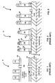
- Fig. 1 illustrates a cross-section view of a layer stack 20, representing some of the layers formed during the fabrication of a typical semiconductor integrated circuit.
- IC semiconductor integrated circuit
- the discussion herein also pertains to substrates employed to fabricate other electronic components, e.g., glass panels employed to fabricate flat panel displays. It should be noted that other additional layers above, below, or between the layers shown may be present. Further, not all of the shown layers need necessarily be present and some or all may be substituted by other different layers.
- a substrate 100 At the bottom of layer stack 20, there is shown a substrate 100.
- An oxide layer 102 typically comprising SiO 2 , may be formed above substrate 100.
- a barrier layer 104 typically formed of a titanium-containing layer such as Ti, TiW, TiN or other suitable barrier materials, may be disposed between oxide layer 102 and a subsequently deposited metallization layer 106.
- barrier layer 104 represents a two-layer structure, which includes a Ti layer underlying a TiN layer. Barrier layer 104, when provided, functions to prevent the diffusion of silicon atoms from oxide layer 102 into the aluminum-containing layer.
- Aluminum-containing layer 106 may represent a layer of pure aluminum or may represent a layer formed of one of the known aluminum alloys such as Al-Cu, Al-Si, or Al-Cu-Si.
- the remaining two layers of Fig. 1, i.e., an anti-reflective coating (ARC) layer 108 and an overlying photoresist (PR) layer 110, may then be formed atop aluminum-containing layer 106.
- the ARC layer 108 typically comprising another titanium-containing layer such as TiN or TiW, may help prevent light (e.g., from the lithography step that patterns the photoresist) from being reflected and scattered off the surface of the aluminum-containing layer 106.
- Photoresist layer 110 represents a layer of conventional photoresist material, which may be patterned for etching, e.g., through exposure to ultraviolet rays.
- the layers of particular interest to the present invention are aluminum-containing layer 106 and photoresist layer 110, with all other layers being optional.
- the layers of layer stack 20 are readily recognizable to those skilled in the art and may be formed using any of a number of suitable and known deposition processes, including chemical vapor deposition (CVD), plasma-enhanced chemical vapor deposition (PECVD), and physical vapor deposition (PVD) such as sputtering.
- CVD chemical vapor deposition
- PECVD plasma-enhanced chemical vapor deposition
- PVD physical vapor deposition
- a portion of the layers of the layer stack, including aluminum-containing layer 106 may be etched using a suitable photoresist technique.
- a photoresist technique involves the patterning of photoresist layer 110 by exposing the photoresist material in a contact or stepper lithography system, and the development of the photoresist material to form a mask to facilitate subsequent etching.
- an appropriate etchant the areas of the aluminum-containing layer that are unprotected by the mask may then be etched away using an appropriate etching source gas, leaving behind aluminum-containing interconnect lines or features.
- a commonly employed etchant for plasma etching the aluminum layer is a mixture of Cl 2 and BCl 3 .
- modem semiconductor devices are scaled with increasingly narrower etch geometries.
- the feature sizes i.e., the width of the interconnect lines or the spacings (e.g., trenches) between adjacent interconnect lines, have steadily decreased.
- a line width of approximately 0.8 microns ( ⁇ m) is considered acceptable in a 4 megabit (Mb) dynamic random access memory (DRAM) IC
- 256 Mb DRAM IC's preferably employ interconnect lines as thin as 0.25 micrometers or even thinner.
- photoresist selectivity is an etch result that process engineers constantly strive to improve.
- Photoresist selectivity refers to the ability of a given etch process to discriminate between the target layer to be etched (the aluminum-containing layer in this case) and the photoresist mask.
- Photoresist selectivity is frequently expressed in terms of the etch rate through the target layer versus the etch rate of the photoresist mask.
- Photoresist selectivity is quite important since the photoresist mask employed in the fabrication of modem semiconductor devices is quite thin. If a chosen etch process has too low a photoresist selectivity, the photoresist mask may be worn away before the etch is completed, causing etch damage to occur in regions of the underlying aluminum-containing layer where no etching is intended.
- Micromasking residue is another important etch result that needs attention.
- it is desirable that the chosen etch process does not leave unwanted residues or etch byproducts on the surface of the substrate after etching. This is because the presence of the unwanted residue may interfere with subsequent processing steps and/or with the proper performance of the resultant semiconductor device.
- Another important etch parameter is the etch rate through the aluminum-containing layer. Since a higher aluminum etch rate is advantageous from a cost of ownership standpoint (i.e., the production cost per substrate), a higher aluminum etch rate is generally desirable.
- Profile microloading occurs because the etching that occurs in the narrow spacings may differ from one that occurs in the open field regions. This difference may cause the sidewall profile of features in the dense region to assume a different shape from the sidewall profile of features in the open field region.
- profile microloading causes a sidewall 202 and a sidewall 206 in the open field region to assume a more tapered profile than the more vertical sidewall 204 in the dense region.
- Fig. 2 represents the result after the layer stack of Fig. 1 has been etched with the prior art Cl 2 /BCl 3 etchant source gas in a plasma processing chamber.
- profile microloading represents an aberration in the critical dimension of the etched features, it is generally desirable to minimize profile microloading.
- the invention relates to a method according to claims 1-13 for etching selected portions of an aluminum-containing layer of a layer stack that is disposed on a substrate.
- the etch through the aluminum-containing layer is optimized by etching the substrate in a plasma processing chamber using an etchant source gas that includes HCl, a chlorine-containing source gas, and an oxygen-containing source gas.
- the chlorine-containing source gas represents any chlorine-containing gas such as, for example, Cl 2 , CCl 4 , or the like (but not HCl).
- the oxygen-containing source gas may include CO, CO 2 , NO x , O 2 , or the like (either alone or in combination with a diluent such as N 2 , Ar, or preferably He, or the like).
- the etchant source gas employed includes HCl, Cl 2 , and O 2 , with the O 2 flow being limited to below about 20% of the total gas flow into the plasma processing chamber.
- the addition of the O 2 gas surprisingly reduces the photoresist etch rate.
- the reduction of the photoresist etch rate is said to be surprising since the photoresist mask is typically organic-based, and the addition of an oxygen-containing gas that dissociates and forms oxygen plasma should therefore accelerate the burning or removal of the photoresist.
- oxygen is widely employed in the prior art as one of the source gases employed in downstream photoresist stripping processes, i.e., the processes designed to quickly etch away the photoresist mask.
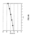
- Fig. 4 wherein the photoresist etch rate on a test wafer having thereon only a layer of blanket deposited I-line photoresist is shown relative to the flow rate of oxygen (expressed as a percentage of the total flow rate of the HCl/Cl 2 /O 2 mixture).
- the flow rate of oxygen expressed as a percentage of the total flow rate of the HCl/Cl 2 /O 2 mixture.
- the aluminum etch rate decreases (due to the formation of relatively stable Al 2 O 3 ) and the photoresist etch rate increases with increasing oxygen flow.
- the aluminum etch rate and the photoresist etch rate behave in a totally unexpected manner when the oxygen flow is below the break point (about 5% of total flow volume in the example of Fig. 4B). That is, in the regime wherein the oxygen flow rate is below the break point, the aluminum etch rate does not decrease while the photoresist etch rate actually decreases.
- the etchant source gas is substantially free of BCl 3 .
- good etch results in terms of the aluminum etch rate, photoresist selectivity, profile microloading, micromasking residue, and the like, have been achieved with the addition of O 2 using the disclosed etch regime and in the absence of BCl 3 . This is so even though BCl 3 is not present to passivate the etch features, as in the case of the prior art Cl 2 /BCl 3 etch.
- aluminum oxide is a very stable compound. Outside of the semiconductor area, it is widely known that aluminum oxide allows aluminum components to be highly resistant to corrosion damage since the durable coating of aluminum oxide, which is formed when aluminum reacts with oxygen in the ambient environment, coats the aluminum surface and stops any further corrosion. Since an oxygen-containing source gas is introduced into the etch source gas mix, one would expect that aluminum oxide, which is also relatively nonvolatile, would be formed and there would be aluminum oxide residue on the wafer surface after etching. Nevertheless, in the etch regime disclosed herein, there is surprisingly little, if any, residue formed on the substrate surface after etching.
- the flow rate of the oxygen-containing source gas plays a crucial role in the success of the aluminum etch.
- the flow rate of the oxygen-containing source gas is below about 20% (but not at 0%) of the total etchant source gas flow rate, more preferably below about 10% (but not at 0%) and most preferably between about 2% and about 4%.
- Figs. 5-8 illustrate some of the etch results for an exemplary etch wherein a mixture of HCl/Cl 2 , and O 2 is employed as the etchant source gas in an inductively coupled, low pressure, high density plasma processing chamber.
- Fig. 5 depicts the relationship between residue remaining (shown in an arbitrary scale on the y axis) and the flow rate of oxygen (expressed as a percentage of the total flow rate on the x axis) for one exemplary recipe. As can be seen, the residue increases significantly when the flow rate of oxygen increases. Below a certain flow rate (4% in the example of Fig. 5), the residue is however surprisingly preferably below about 10% (but not at 0%) and most preferably between about 2% and about 4%.
- Figs. 5-8 illustrate some of the etch results for an exemplary etch wherein a mixture of HCl/Cl 2 , and O 2 is employed as the etchant source gas in an inductively coupled, low pressure, high density plasma processing chamber.
- Fig. 5 depicts the relationship between residue remaining (shown in an arbitrary scale on the y axis) and the flow rate of oxygen (expressed as a percentage of the total flow rate on the x axis) for one exemplary recipe. As can be seen, the residue increases significantly when the flow rate of oxygen increases. Below a certain flow rate (4% in the example of Fig. 5), the residue is however surprisingly absent.
- Fig. 5 depicts the relationship between residue remaining (shown in an arbitrary scale on the y axis) and the flow rate of oxygen (expressed as a percentage of the total flow rate on the x axis) for one exemplary recipe. As can be seen, the residue increases significantly when the flow rate of oxygen increases. Below a certain flow rate (4% in the
- FIG. 6 depicts the relationship between the photoresist etch rate (in angstroms per minute) and the flow rate of oxygen (again expressed as a percentage of the total flow rate).
- the photoresist etch rate surprisingly decreases as the oxygen flow rate increases in the regime shown (e.g., between about 2% and about 6% in the example of Fig. 6).
- Fig. 7 depicts the relationship between the photoresist selectivity (i.e., aluminum etch rate relative to photoresist etch rate) and the flow rate of oxygen (again expressed as a percentage of the total flow rate).
- the photoresist seiectivity increases as the flow rate of oxygen is increased in the exemplary regime of the figure (i.e., between about 2% and about 6%).
- Fig. 8 depicts the relationship between the profile microloading and the flow rate of oxygen (again expressed as a percentage of the total flow rate). As the example of Fig. 8 shows, the profile microloading decreases as the flow rate of oxygen is increased in the exemplary regime of the figure (i.e., between about 2% and about 6%). Decreasing profile microloading in the disclosed etch regime is another advantage of the inventive etch process.
- high density refers to a plasma density above about 10 11 ions/cm 3 while low pressure refers to the fact that pressure within the plasma chamber is below about 100 m Torr (13,33 Pa) during etching.
- the invention is of course not limited to any particular type of photoresist material or wafer size, and it is contemplated that the invention may well be practiced in other types of plasma processing reactors, including those having higher pressures and medium or low density plasma.
- the bottom electrode power may be between about 80 watts and about 300 watts, more preferably between about 100 watts and about 220 watts, and preferably at about 160 watts.
- the bottom electrode power is a critical parameter because it controls the rate of residue sputtering, as mentioned earlier. It is contemplated that this value, as well as other values disclosed herein, may be optimized to suit the requirements of a particular plasma processing system, a particular substrate size, or a particular type of photoresist and/or aluminum-containing layer. Such optimization is within the ability of one of ordinary skills in the art given this disclosure.
- the top electrode power may be between about 400 watts and about 1,200 watts, more preferably between about 600 watts and about 1,000 watts, and preferably at about 800 watts.
- the pressure in the plasma chamber during etching may be between about 2 mTorr (0,27 Pa) and about 20 mTorr (2,7 Pa) more preferably between about 8 mTorr (1,066 Pa) and about 12 mTorr (1,6 Pa), and preferably at about 10 mTorr (1,33 Pa). The pressure is a critical parameter since it impacts the resident time of the plasma.
- the total flow rate of the HCl/chlorine-containing source gas/oxygen containing source gas (e.g., HCL/Cl 2 /O 2 ) etchant source gas may be between about 50 standard cubic centimeters per minute (sccm) and about 300 sccm, more preferably between about 100 sccm and about 200 sccm, and preferably at about 150 sccm.
- the ratio of the chlorine-containing source gas (e.g., Cl 2 ) to HCl may be between about 0.1:1 and about 10:1, more preferably between about 0.25:1 and about 4:1, and preferably at about 2:1.
- the flow rate of the oxygen-containing gas (e.g., O 2 ) as a percentage of the total flow rate may be between about 0% (but not at 0%) and about 20%, more preferably between about 0% (but not at 0%) and about 10%, and even more preferably between about 2% and about 4%.
- the oxygen flow rate is a critical parameter since it produces the surprising result of lowering the photoresist etch rate and forming surprisingly little, if any, residue in the disclosed etch regime.
- the electrode temperature may be between about 20°C and about 80°C, more preferably between about 40°C and about 60°C, and preferably at about 50°C.
- the etchant source gas includes Cl 2 /HCl/CO 2 with the CO 2 representing the oxygen-containing gas. It has been found that when CO 2 is employed as the oxygen-containing gas in the Cl 2 /HCl/O 2 etch of the aluminum-containing layer, a wider process window can be achieved, i.e., the process is more forgiving by yielding good results, particularly with respect to residue issues, while allowing a wider range of parameters.
- the etchant source gas preferably consists essentially of the aforementioned Cl 2 /HCL/CO 2 component gases and is substantially free of BCl 3 or consists essentially of the aforementioned Cl 2 /HCL/CO 2 component gases and a diluent gas (such as N 2 , Ar or preferably He) and is substantially free of BCl 3 .
- a low pressure, high density 9600 PTXTM plasma processing system is employed for the exemplary etch although it is contemplated that the invention may well be practiced in other types of plasma processing reactors, including those having higher pressures and medium or low density plasma.
- the bottom electrode power may be between about 50 watts and about 300 watts, more preferably between about 50 watts and about 250 watts, and preferably about 100 watts to about 200 watts, with about 150 watts being the preferred value.
- the sheath voltage may be at about -85 volts to about -145 volts, with the preferred value at about -115 volts.
- the bottom electrode power and/or sheath voltage is important since they (together or individually) control the rate of residue sputtering.
- the top electrode power may be between about 300 watts and about 900 watts, and preferably at about 600 watts.
- the pressure in the plasma chamber during etching may be between about 6 mTorr (0,8 Pa) and about 14 mTorr (1,87 Pa) and preferably at about 10 mTorr (1,33 Pa). The pressure is a critical parameter since it impacts the resident time of the plasma.
- the total flow rate of the HCl/chlorine-containing source gas/oxygen containing source gas (e.g., HCL/Cl 2 /CO 2 ) etchant source gas may be between about 50 standard cubic centimeters per minute (sccm) and about 300 sccm, more preferably between about 100 sccm and about 200 sccm, and preferably at about 150 sccm.
- the ratio of the chlorine-containing source gas (e.g., Cl 2 ) to HCl may be between about 0.1:1 and about 10:1, more preferably between about 0.25:1 and about 4:1, and preferably at about 2:1.
- the flow rate of the oxygen-containing gas as a percentage of the total flow rate may be between about 0% (but not at 0%) and about 50%, more preferably between about 0% (but not at 0%) and about 20%, even more preferably between about 1% and about 12%, and even more preferably between about 5% and about 7%, with about 6% being the preferred midpoint.
- the flow rate of the CO 2 is a critical parameter since it produces the surprising result of lowering the photoresist etch rate and forming surprisingly little, if any, residue in the disclosed etch regime.
- the electrode temperature may be between about 20°C and about 80°C, more preferably between about 40°C and about 60°C, and preferably at about 50°C.
- the chamber temperature is. in one embodiment, about 70 °C, with the He clamp pressure at about 10 Torr (1,33 Pa).
Description
| PROCESS | Cl2/BCl3 | HCl/Cl2/O2 |
| Aluminum Etch Rate in Angstroms Per Minute | about 14,000 | about 18,000 |
| Photoresist Etch Rate in Angstroms Per Minute (For I-line photoresist) | about 4,400 | about 3,200 |
| Photoresist Selectivity | 3.1:1 | 5.6:1 |
| | 15% | 7% |
Claims (13)
- A method for etching selected portions of an aluminium-containing layer of a layer stack, said layer stack being disposed on a substrate, said aluminium-containing layer being disposed below a photoresist mask having a pattern thereon, comprising:providing a plasma processing chamber;positioning said substrate having thereon said layer stack, including said aluminium containing layer and said photoresist mask, within said plasma processing chamber;flowing an etchant source gas that comprises HCl, a chlorine-containing source gas, and an oxygen-containing source gas into said plasma processing chamber; wherein a flow rate of said oxygen-containing source gas is less than 20 percent of a total flow rate of said etchant source gas, and wherein said etchant source gas is substantially free of BCl3;striking a plasma out of said etchant source gas, wherein said plasma is employed to etch at least partially through said aluminium-containing layer.
- The method of claim 1 wherein said oxygen-containing source gas is CO2.
- The method of any of claim 1 wherein said oxygen-containing source gas represents a mixture of CO2 and a diluent gas.
- The method of claim 3 wherein the diluent gas is He.
- The method of claim 1 wherein the oxygen-containing source gas is O2.
- The method of any of claims 1 to 5 wherein said chlorine-containing source gas is Cl2.
- The method of any of claims 1 to 6 wherein said plasma has a density of at least 1011 ions/cm3,
- The method of any of claims 1 to 7 wherein said flow rate of said oxygen-containing source gas is between 1 and 12 percent of said total flow rate.
- The method of any of claims 1 to 7 wherien said flow rate of said oxygen-containing source gas is between 5 percent and 7 percent of said total flow rate.
- The method of any of claims 1 to 9 wherein a top power setting for said plasma processing chamber is between 300 W and 900 W.
- The method of any of claims 1 to 10 wherein said pressure is between 6 mTorr and 14 mTorr. (0,8 and 1,87 Pa).
- The method of any of claims 1 to 11, wherein said plasma processing chamber is an inductively coupled plasma processing chamber.
- The method of any of claims 1 to 12, wherein the plasma is a low pressure high density plasma.
Priority Applications (1)
| Application Number | Priority Date | Filing Date | Title |
|---|---|---|---|
| EP04254796A EP1475461A1 (en) | 1998-06-24 | 1999-06-22 | Methods for etching an aluminum-containing layer |
Applications Claiming Priority (3)
| Application Number | Priority Date | Filing Date | Title |
|---|---|---|---|
| US103498 | 1998-06-24 | ||
| US09/103,498 US5994235A (en) | 1998-06-24 | 1998-06-24 | Methods for etching an aluminum-containing layer |
| PCT/US1999/014026 WO1999067443A1 (en) | 1998-06-24 | 1999-06-22 | Methods for etching an aluminum-containing layer |
Related Child Applications (1)
| Application Number | Title | Priority Date | Filing Date |
|---|---|---|---|
| EP04254796A Division EP1475461A1 (en) | 1998-06-24 | 1999-06-22 | Methods for etching an aluminum-containing layer |
Publications (2)
| Publication Number | Publication Date |
|---|---|
| EP1097257A1 EP1097257A1 (en) | 2001-05-09 |
| EP1097257B1 true EP1097257B1 (en) | 2004-12-15 |
Family
ID=22295515
Family Applications (2)
| Application Number | Title | Priority Date | Filing Date |
|---|---|---|---|
| EP99931856A Expired - Lifetime EP1097257B1 (en) | 1998-06-24 | 1999-06-22 | Methods for etching an aluminum-containing layer |
| EP04254796A Withdrawn EP1475461A1 (en) | 1998-06-24 | 1999-06-22 | Methods for etching an aluminum-containing layer |
Family Applications After (1)
| Application Number | Title | Priority Date | Filing Date |
|---|---|---|---|
| EP04254796A Withdrawn EP1475461A1 (en) | 1998-06-24 | 1999-06-22 | Methods for etching an aluminum-containing layer |
Country Status (8)
| Country | Link |
|---|---|
| US (2) | US5994235A (en) |
| EP (2) | EP1097257B1 (en) |
| JP (1) | JP2002519841A (en) |
| KR (1) | KR100645908B1 (en) |
| DE (1) | DE69922658T2 (en) |
| ES (1) | ES2233055T3 (en) |
| TW (1) | TW421828B (en) |
| WO (1) | WO1999067443A1 (en) |
Families Citing this family (24)
| Publication number | Priority date | Publication date | Assignee | Title |
|---|---|---|---|---|
| US7023021B2 (en) | 2000-02-22 | 2006-04-04 | Semiconductor Energy Laboratory Co., Ltd. | Semiconductor device and method of manufacturing the same |
| US6789910B2 (en) | 2000-04-12 | 2004-09-14 | Semiconductor Energy Laboratory, Co., Ltd. | Illumination apparatus |
| US7115523B2 (en) * | 2000-05-22 | 2006-10-03 | Applied Materials, Inc. | Method and apparatus for etching photomasks |
| US6391790B1 (en) | 2000-05-22 | 2002-05-21 | Applied Materials, Inc. | Method and apparatus for etching photomasks |
| EP1290495A2 (en) * | 2000-06-15 | 2003-03-12 | Applied Materials, Inc. | A method and apparatus for etching metal layers on substrates |
| US7084066B1 (en) * | 2000-07-03 | 2006-08-01 | Cypress Semiconductor Corporation | Method of uniformly etching refractory metals, refractory metal alloys and refractory metal silicides |
| JP4605554B2 (en) * | 2000-07-25 | 2011-01-05 | 独立行政法人物質・材料研究機構 | Mask material for dry etching |
| US6551942B2 (en) | 2001-06-15 | 2003-04-22 | International Business Machines Corporation | Methods for etching tungsten stack structures |
| US20030003374A1 (en) * | 2001-06-15 | 2003-01-02 | Applied Materials, Inc. | Etch process for photolithographic reticle manufacturing with improved etch bias |
| US7183201B2 (en) | 2001-07-23 | 2007-02-27 | Applied Materials, Inc. | Selective etching of organosilicate films over silicon oxide stop etch layers |
| WO2003021659A1 (en) * | 2001-09-04 | 2003-03-13 | Applied Materials, Inc. | Methods and apparatus for etching metal layers on substrates |
| WO2003089990A2 (en) * | 2002-04-19 | 2003-10-30 | Applied Materials, Inc. | Process for etching photomasks |
| KR20040012451A (en) * | 2002-05-14 | 2004-02-11 | 어플라이드 머티어리얼스, 인코포레이티드 | Methods for etching photolithographic reticles |
| KR100464430B1 (en) * | 2002-08-20 | 2005-01-03 | 삼성전자주식회사 | Method of etching aluminum layer using hard mask and metalization method for semiconductor device |
| US7270761B2 (en) * | 2002-10-18 | 2007-09-18 | Appleid Materials, Inc | Fluorine free integrated process for etching aluminum including chamber dry clean |
| US6960413B2 (en) * | 2003-03-21 | 2005-11-01 | Applied Materials, Inc. | Multi-step process for etching photomasks |
| US7077973B2 (en) * | 2003-04-18 | 2006-07-18 | Applied Materials, Inc. | Methods for substrate orientation |
| US20040229470A1 (en) * | 2003-05-14 | 2004-11-18 | Applied Materials, Inc. | Method for etching an aluminum layer using an amorphous carbon mask |
| US7521000B2 (en) * | 2003-08-28 | 2009-04-21 | Applied Materials, Inc. | Process for etching photomasks |
| US7829243B2 (en) * | 2005-01-27 | 2010-11-09 | Applied Materials, Inc. | Method for plasma etching a chromium layer suitable for photomask fabrication |
| US8293430B2 (en) * | 2005-01-27 | 2012-10-23 | Applied Materials, Inc. | Method for etching a molybdenum layer suitable for photomask fabrication |
| US7435681B2 (en) * | 2006-05-09 | 2008-10-14 | Macronix International Co., Ltd. | Methods of etching stacks having metal layers and hard mask layers |
| KR100944846B1 (en) * | 2006-10-30 | 2010-03-04 | 어플라이드 머티어리얼스, 인코포레이티드 | Mask etch process |
| US8808562B2 (en) | 2011-09-12 | 2014-08-19 | Tokyo Electron Limited | Dry metal etching method |
Family Cites Families (10)
| Publication number | Priority date | Publication date | Assignee | Title |
|---|---|---|---|---|
| IT1203089B (en) * | 1976-03-03 | 1989-02-15 | Int Plasma Corp | PROCEDURE AND EQUIPMENT TO PERFORM CHEMICAL REACTIONS IN THE REGION OF THE LUMINESCENT DISCHARGE OF A PLASMA |
| US4256534A (en) * | 1978-07-31 | 1981-03-17 | Bell Telephone Laboratories, Incorporated | Device fabrication by plasma etching |
| JPS57170534A (en) * | 1981-04-15 | 1982-10-20 | Hitachi Ltd | Dry etching method for aluminum and aluminum alloy |
| JPS58213877A (en) * | 1982-06-05 | 1983-12-12 | Anelva Corp | Method for dry etching aluminum |
| US4462882A (en) * | 1983-01-03 | 1984-07-31 | Massachusetts Institute Of Technology | Selective etching of aluminum |
| DE4107006A1 (en) * | 1991-03-05 | 1992-09-10 | Siemens Ag | METHOD FOR ANISOTROPICALLY DRYING ALUMINUM OR BZW. ALUMINUM ALLOYS CONTAINING LADDER RAILINGS IN INTEGRATED SEMICONDUCTOR CIRCUITS |
| JP3225532B2 (en) * | 1991-03-29 | 2001-11-05 | ソニー株式会社 | Dry etching method |
| US5387556A (en) * | 1993-02-24 | 1995-02-07 | Applied Materials, Inc. | Etching aluminum and its alloys using HC1, C1-containing etchant and N.sub.2 |
| JPH08130206A (en) * | 1994-10-31 | 1996-05-21 | Sony Corp | Plasma etching method of al based metal layer |
| US5976986A (en) * | 1996-08-06 | 1999-11-02 | International Business Machines Corp. | Low pressure and low power C12 /HC1 process for sub-micron metal etching |
-
1998
- 1998-06-24 US US09/103,498 patent/US5994235A/en not_active Expired - Lifetime
-
1999
- 1999-06-22 DE DE69922658T patent/DE69922658T2/en not_active Expired - Fee Related
- 1999-06-22 EP EP99931856A patent/EP1097257B1/en not_active Expired - Lifetime
- 1999-06-22 EP EP04254796A patent/EP1475461A1/en not_active Withdrawn
- 1999-06-22 ES ES99931856T patent/ES2233055T3/en not_active Expired - Lifetime
- 1999-06-22 JP JP2000556081A patent/JP2002519841A/en active Pending
- 1999-06-22 KR KR1020007014489A patent/KR100645908B1/en not_active IP Right Cessation
- 1999-06-22 WO PCT/US1999/014026 patent/WO1999067443A1/en active IP Right Grant
- 1999-06-23 TW TW088110580A patent/TW421828B/en not_active IP Right Cessation
- 1999-06-24 US US09/344,168 patent/US6242107B1/en not_active Expired - Lifetime
Also Published As
| Publication number | Publication date |
|---|---|
| US6242107B1 (en) | 2001-06-05 |
| DE69922658T2 (en) | 2005-12-08 |
| US5994235A (en) | 1999-11-30 |
| EP1097257A1 (en) | 2001-05-09 |
| ES2233055T3 (en) | 2005-06-01 |
| DE69922658D1 (en) | 2005-01-20 |
| WO1999067443A1 (en) | 1999-12-29 |
| KR100645908B1 (en) | 2006-11-17 |
| TW421828B (en) | 2001-02-11 |
| WO1999067443A9 (en) | 2000-06-08 |
| EP1475461A1 (en) | 2004-11-10 |
| KR20010053044A (en) | 2001-06-25 |
| JP2002519841A (en) | 2002-07-02 |
Similar Documents
| Publication | Publication Date | Title |
|---|---|---|
| EP1097257B1 (en) | Methods for etching an aluminum-containing layer | |
| US6090717A (en) | High density plasma etching of metallization layer using chlorine and nitrogen | |
| EP0880799B1 (en) | Methods for etching semiconductor wafers | |
| JP4690512B2 (en) | Method for reducing polymer deposition on etched vertical metal lines, corrosion of etched metal lines and corrosion during wet cleaning of etched metal features | |
| US7482279B2 (en) | Method for fabricating semiconductor device using ArF photolithography capable of protecting tapered profile of hard mask | |
| US5883007A (en) | Methods and apparatuses for improving photoresist selectivity and reducing etch rate loading | |
| JP2003506866A (en) | Sidewall polymer forming gas additive for etching process | |
| EP0644582B1 (en) | Dry etching method | |
| US6103457A (en) | Method for reducing faceting on a photoresist layer during an etch process | |
| US7413992B2 (en) | Tungsten silicide etch process with reduced etch rate micro-loading | |
| US5846443A (en) | Methods and apparatus for etching semiconductor wafers and layers thereof | |
| US6057240A (en) | Aqueous surfactant solution method for stripping metal plasma etch deposited oxidized metal impregnated polymer residue layers from patterned metal layers | |
| US7226867B2 (en) | Method of etching a metal layer using a mask, a metallization method for a semiconductor device, a method of etching a metal layer, and an etching gas | |
| KR100268640B1 (en) | Dry etching method of aluminum alloy film and etching gas used in the method | |
| JPH1027804A (en) | Semiconductor device and manufacture thereof | |
| US7435681B2 (en) | Methods of etching stacks having metal layers and hard mask layers | |
| JPH07106308A (en) | Dry etching method | |
| JPH0637058A (en) | Dry etching method | |
| JPH05182938A (en) | Dry-etching method |
Legal Events
| Date | Code | Title | Description |
|---|---|---|---|
| PUAI | Public reference made under article 153(3) epc to a published international application that has entered the european phase |
Free format text: ORIGINAL CODE: 0009012 |
|
| 17P | Request for examination filed |
Effective date: 20010104 |
|
| AK | Designated contracting states |
Kind code of ref document: A1 Designated state(s): DE ES FR GB IT NL |
|
| RIN1 | Information on inventor provided before grant (corrected) |
Inventor name: O'DONNELL, ROBERT J. |
|
| 17Q | First examination report despatched |
Effective date: 20010515 |
|
| GRAP | Despatch of communication of intention to grant a patent |
Free format text: ORIGINAL CODE: EPIDOSNIGR1 |
|
| GRAS | Grant fee paid |
Free format text: ORIGINAL CODE: EPIDOSNIGR3 |
|
| GRAA | (expected) grant |
Free format text: ORIGINAL CODE: 0009210 |
|
| AK | Designated contracting states |
Kind code of ref document: B1 Designated state(s): DE ES FR GB IT NL |
|
| REG | Reference to a national code |
Ref country code: GB Ref legal event code: FG4D |
|
| REF | Corresponds to: |
Ref document number: 69922658 Country of ref document: DE Date of ref document: 20050120 Kind code of ref document: P |
|
| REG | Reference to a national code |
Ref country code: ES Ref legal event code: FG2A Ref document number: 2233055 Country of ref document: ES Kind code of ref document: T3 |
|
| PLBE | No opposition filed within time limit |
Free format text: ORIGINAL CODE: 0009261 |
|
| STAA | Information on the status of an ep patent application or granted ep patent |
Free format text: STATUS: NO OPPOSITION FILED WITHIN TIME LIMIT |
|
| 26N | No opposition filed |
Effective date: 20050916 |
|
| ET | Fr: translation filed | ||
| PGFP | Annual fee paid to national office [announced via postgrant information from national office to epo] |
Ref country code: NL Payment date: 20060624 Year of fee payment: 8 |
|
| PGFP | Annual fee paid to national office [announced via postgrant information from national office to epo] |
Ref country code: GB Payment date: 20060626 Year of fee payment: 8 Ref country code: ES Payment date: 20060626 Year of fee payment: 8 |
|
| PGFP | Annual fee paid to national office [announced via postgrant information from national office to epo] |
Ref country code: DE Payment date: 20060731 Year of fee payment: 8 |
|
| PGFP | Annual fee paid to national office [announced via postgrant information from national office to epo] |
Ref country code: IT Payment date: 20070625 Year of fee payment: 9 |
|
| GBPC | Gb: european patent ceased through non-payment of renewal fee |
Effective date: 20070622 |
|
| NLV4 | Nl: lapsed or anulled due to non-payment of the annual fee |
Effective date: 20080101 |
|
| PG25 | Lapsed in a contracting state [announced via postgrant information from national office to epo] |
Ref country code: NL Free format text: LAPSE BECAUSE OF NON-PAYMENT OF DUE FEES Effective date: 20080101 Ref country code: DE Free format text: LAPSE BECAUSE OF NON-PAYMENT OF DUE FEES Effective date: 20080101 |
|
| PGFP | Annual fee paid to national office [announced via postgrant information from national office to epo] |
Ref country code: FR Payment date: 20070618 Year of fee payment: 9 |
|
| PG25 | Lapsed in a contracting state [announced via postgrant information from national office to epo] |
Ref country code: GB Free format text: LAPSE BECAUSE OF NON-PAYMENT OF DUE FEES Effective date: 20070622 |
|
| REG | Reference to a national code |
Ref country code: ES Ref legal event code: FD2A Effective date: 20070623 |
|
| PG25 | Lapsed in a contracting state [announced via postgrant information from national office to epo] |
Ref country code: ES Free format text: LAPSE BECAUSE OF NON-PAYMENT OF DUE FEES Effective date: 20070623 |
|
| REG | Reference to a national code |
Ref country code: FR Ref legal event code: ST Effective date: 20090228 |
|
| PG25 | Lapsed in a contracting state [announced via postgrant information from national office to epo] |
Ref country code: IT Free format text: LAPSE BECAUSE OF NON-PAYMENT OF DUE FEES Effective date: 20080622 Ref country code: FR Free format text: LAPSE BECAUSE OF NON-PAYMENT OF DUE FEES Effective date: 20080630 |