EP1087440A2 - Modeling technique to increase device reliability - Google Patents
Modeling technique to increase device reliability Download PDFInfo
- Publication number
- EP1087440A2 EP1087440A2 EP00307830A EP00307830A EP1087440A2 EP 1087440 A2 EP1087440 A2 EP 1087440A2 EP 00307830 A EP00307830 A EP 00307830A EP 00307830 A EP00307830 A EP 00307830A EP 1087440 A2 EP1087440 A2 EP 1087440A2
- Authority
- EP
- European Patent Office
- Prior art keywords
- row
- balls
- grid array
- ball
- technique
- Prior art date
- Legal status (The legal status is an assumption and is not a legal conclusion. Google has not performed a legal analysis and makes no representation as to the accuracy of the status listed.)
- Withdrawn
Links
Images


Classifications
-
- H—ELECTRICITY
- H05—ELECTRIC TECHNIQUES NOT OTHERWISE PROVIDED FOR
- H05K—PRINTED CIRCUITS; CASINGS OR CONSTRUCTIONAL DETAILS OF ELECTRIC APPARATUS; MANUFACTURE OF ASSEMBLAGES OF ELECTRICAL COMPONENTS
- H05K1/00—Printed circuits
- H05K1/02—Details
- H05K1/11—Printed elements for providing electric connections to or between printed circuits
- H05K1/111—Pads for surface mounting, e.g. lay-out
- H05K1/112—Pads for surface mounting, e.g. lay-out directly combined with via connections
-
- H—ELECTRICITY
- H01—ELECTRIC ELEMENTS
- H01L—SEMICONDUCTOR DEVICES NOT COVERED BY CLASS H10
- H01L23/00—Details of semiconductor or other solid state devices
- H01L23/48—Arrangements for conducting electric current to or from the solid state body in operation, e.g. leads, terminal arrangements ; Selection of materials therefor
- H01L23/488—Arrangements for conducting electric current to or from the solid state body in operation, e.g. leads, terminal arrangements ; Selection of materials therefor consisting of soldered or bonded constructions
- H01L23/498—Leads, i.e. metallisations or lead-frames on insulating substrates, e.g. chip carriers
- H01L23/49838—Geometry or layout
-
- H—ELECTRICITY
- H01—ELECTRIC ELEMENTS
- H01L—SEMICONDUCTOR DEVICES NOT COVERED BY CLASS H10
- H01L2224/00—Indexing scheme for arrangements for connecting or disconnecting semiconductor or solid-state bodies and methods related thereto as covered by H01L24/00
- H01L2224/01—Means for bonding being attached to, or being formed on, the surface to be connected, e.g. chip-to-package, die-attach, "first-level" interconnects; Manufacturing methods related thereto
- H01L2224/26—Layer connectors, e.g. plate connectors, solder or adhesive layers; Manufacturing methods related thereto
- H01L2224/31—Structure, shape, material or disposition of the layer connectors after the connecting process
- H01L2224/32—Structure, shape, material or disposition of the layer connectors after the connecting process of an individual layer connector
- H01L2224/321—Disposition
- H01L2224/32151—Disposition the layer connector connecting between a semiconductor or solid-state body and an item not being a semiconductor or solid-state body, e.g. chip-to-substrate, chip-to-passive
- H01L2224/32221—Disposition the layer connector connecting between a semiconductor or solid-state body and an item not being a semiconductor or solid-state body, e.g. chip-to-substrate, chip-to-passive the body and the item being stacked
- H01L2224/32225—Disposition the layer connector connecting between a semiconductor or solid-state body and an item not being a semiconductor or solid-state body, e.g. chip-to-substrate, chip-to-passive the body and the item being stacked the item being non-metallic, e.g. insulating substrate with or without metallisation
-
- H—ELECTRICITY
- H01—ELECTRIC ELEMENTS
- H01L—SEMICONDUCTOR DEVICES NOT COVERED BY CLASS H10
- H01L2224/00—Indexing scheme for arrangements for connecting or disconnecting semiconductor or solid-state bodies and methods related thereto as covered by H01L24/00
- H01L2224/01—Means for bonding being attached to, or being formed on, the surface to be connected, e.g. chip-to-package, die-attach, "first-level" interconnects; Manufacturing methods related thereto
- H01L2224/42—Wire connectors; Manufacturing methods related thereto
- H01L2224/47—Structure, shape, material or disposition of the wire connectors after the connecting process
- H01L2224/48—Structure, shape, material or disposition of the wire connectors after the connecting process of an individual wire connector
- H01L2224/4805—Shape
- H01L2224/4809—Loop shape
- H01L2224/48091—Arched
-
- H—ELECTRICITY
- H01—ELECTRIC ELEMENTS
- H01L—SEMICONDUCTOR DEVICES NOT COVERED BY CLASS H10
- H01L2224/00—Indexing scheme for arrangements for connecting or disconnecting semiconductor or solid-state bodies and methods related thereto as covered by H01L24/00
- H01L2224/01—Means for bonding being attached to, or being formed on, the surface to be connected, e.g. chip-to-package, die-attach, "first-level" interconnects; Manufacturing methods related thereto
- H01L2224/42—Wire connectors; Manufacturing methods related thereto
- H01L2224/47—Structure, shape, material or disposition of the wire connectors after the connecting process
- H01L2224/48—Structure, shape, material or disposition of the wire connectors after the connecting process of an individual wire connector
- H01L2224/481—Disposition
- H01L2224/48151—Connecting between a semiconductor or solid-state body and an item not being a semiconductor or solid-state body, e.g. chip-to-substrate, chip-to-passive
- H01L2224/48221—Connecting between a semiconductor or solid-state body and an item not being a semiconductor or solid-state body, e.g. chip-to-substrate, chip-to-passive the body and the item being stacked
- H01L2224/48225—Connecting between a semiconductor or solid-state body and an item not being a semiconductor or solid-state body, e.g. chip-to-substrate, chip-to-passive the body and the item being stacked the item being non-metallic, e.g. insulating substrate with or without metallisation
- H01L2224/48227—Connecting between a semiconductor or solid-state body and an item not being a semiconductor or solid-state body, e.g. chip-to-substrate, chip-to-passive the body and the item being stacked the item being non-metallic, e.g. insulating substrate with or without metallisation connecting the wire to a bond pad of the item
-
- H—ELECTRICITY
- H01—ELECTRIC ELEMENTS
- H01L—SEMICONDUCTOR DEVICES NOT COVERED BY CLASS H10
- H01L2224/00—Indexing scheme for arrangements for connecting or disconnecting semiconductor or solid-state bodies and methods related thereto as covered by H01L24/00
- H01L2224/73—Means for bonding being of different types provided for in two or more of groups H01L2224/10, H01L2224/18, H01L2224/26, H01L2224/34, H01L2224/42, H01L2224/50, H01L2224/63, H01L2224/71
- H01L2224/732—Location after the connecting process
- H01L2224/73251—Location after the connecting process on different surfaces
- H01L2224/73265—Layer and wire connectors
-
- H—ELECTRICITY
- H01—ELECTRIC ELEMENTS
- H01L—SEMICONDUCTOR DEVICES NOT COVERED BY CLASS H10
- H01L2924/00—Indexing scheme for arrangements or methods for connecting or disconnecting semiconductor or solid-state bodies as covered by H01L24/00
- H01L2924/15—Details of package parts other than the semiconductor or other solid state devices to be connected
- H01L2924/151—Die mounting substrate
- H01L2924/153—Connection portion
- H01L2924/1531—Connection portion the connection portion being formed only on the surface of the substrate opposite to the die mounting surface
- H01L2924/15311—Connection portion the connection portion being formed only on the surface of the substrate opposite to the die mounting surface being a ball array, e.g. BGA
-
- H—ELECTRICITY
- H05—ELECTRIC TECHNIQUES NOT OTHERWISE PROVIDED FOR
- H05K—PRINTED CIRCUITS; CASINGS OR CONSTRUCTIONAL DETAILS OF ELECTRIC APPARATUS; MANUFACTURE OF ASSEMBLAGES OF ELECTRICAL COMPONENTS
- H05K2201/00—Indexing scheme relating to printed circuits covered by H05K1/00
- H05K2201/09—Shape and layout
- H05K2201/09209—Shape and layout details of conductors
- H05K2201/09218—Conductive traces
- H05K2201/09227—Layout details of a plurality of traces, e.g. escape layout for Ball Grid Array [BGA] mounting
-
- H—ELECTRICITY
- H05—ELECTRIC TECHNIQUES NOT OTHERWISE PROVIDED FOR
- H05K—PRINTED CIRCUITS; CASINGS OR CONSTRUCTIONAL DETAILS OF ELECTRIC APPARATUS; MANUFACTURE OF ASSEMBLAGES OF ELECTRICAL COMPONENTS
- H05K2201/00—Indexing scheme relating to printed circuits covered by H05K1/00
- H05K2201/10—Details of components or other objects attached to or integrated in a printed circuit board
- H05K2201/10613—Details of electrical connections of non-printed components, e.g. special leads
- H05K2201/10621—Components characterised by their electrical contacts
- H05K2201/10734—Ball grid array [BGA]; Bump grid array
-
- H—ELECTRICITY
- H05—ELECTRIC TECHNIQUES NOT OTHERWISE PROVIDED FOR
- H05K—PRINTED CIRCUITS; CASINGS OR CONSTRUCTIONAL DETAILS OF ELECTRIC APPARATUS; MANUFACTURE OF ASSEMBLAGES OF ELECTRICAL COMPONENTS
- H05K3/00—Apparatus or processes for manufacturing printed circuits
- H05K3/0005—Apparatus or processes for manufacturing printed circuits for designing circuits by computer
Definitions
- the present invention relates to the field of integrated circuit devices. More specifically, but not exclusively, the present invention relates to a modeling technique for selectively depopulating electrical contacts from a foot print of a grid array (ball grid array (BGA) or land grid array (LGA)) package to increase the routability of the package substrate and increase the device reliability.
- BGA ball grid array
- LGA land grid array
- CSPs chip scale packages
- CSPs are in many ways an ideal solution to the cost reduction and miniaturization requirement. They offer enormous area reductions compared with quad flat package, and have increasing potential to do so without adding system level cost. In the best case, CSPs are able to compete today, on a cost per terminal basis, with quad flat packages. For example, various CSPs from Texas Instruments are now available at cost parity with thin quad flat packages.
- Texas Instruments produces a polyimide-based family of CSPs known as MicroStarBGATM (see Figure 1) .
- This CSP 10 like most others, uses solder alloy balls 12 as the interconnection between the package substrate 14 and the board on which the packages is soldered. As with all such packages, the solder balls formed between the package and the board are susceptible to fatigue when exposed to cyclic ambient temperature conditions.
- JEDEC and EIAJ are increasingly documenting fine pitch BGA industry standards.
- the finest pitch standard that is currently widely recognized is 0.50mm pitch.
- broad acceptance and use of 0.50mm pitch CSPs is still very limited, due to the following reasons:
- Figure 4 discloses a conventional ball footprint (regular pattern of 3 row of balls) having 144 balls (on a 0.5 mm pitch) on a 10x10mm package body. To achieve this dense routing, a designer has to compromise. There are typically three options:
- Figure 5 discloses a routing pattern for 3 full rows of balls, in which:
- An embodiment of the invention provides a modeling technique for selectively depopulating solder contacts (and their respective contact pads, vias and traces or lines) from a conventional foot print of a grid array package (Ball Grid Array (BGA), or Land Grid Array (LGA)) to improve device reliability, and a BGA or LGA package so modeled.
- the modeling technique anticipates a routing of traces through the gap resulting from the depopulated solder contacts as additional space for routing traces or lines from solder contact pads to an exterior surface of a substrate (14) upon which a semiconductor die (20) is mounted.
- An advantage of an embodiment of the present invention is that it provides an easy to use modeling technique (e.g., in this case an Excel spreadsheet) that allows a user to easily predict whether or not a preselected number of balls on a specific body size device will be possible.
- a 280 um via (32) only permits one trace between adjacent balls (12). If however, we depopulate a ball (including its associated via (32), solder ball pad (34) and trace or line (30)), we can now place up to 8 traces or lines (30) when using the 25um rule-line/space 28/42 (or up to 13 traces or lines (30) when using the 18um rule-line/space 20/30 - these numbers will change when other rule-line/space numbers are selected) in the resulting gap between 2 adjacent balls. By careful selection of these depopulated balls, it is possible to route as many, if not more total balls with the optimum design rule (optimum via diameter), as compared to the conventional footprint with compromised design rules (e.g., via diameter of less than 280 um) . This design concept is called 'Smart-Foot'TM, .
- Figure 6 illustrates a footprint (38), with selective ball depopulation. More specifically, the selective ball depopulated footprint (38) shown in Figure 6 is a footprint for the TI 151 GHZ uStarBGA TM, package, which comprises 151 balls on a 10x10 mm body (40).
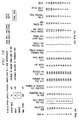
- Figure 7 discloses an Excel spreadsheet incorporating a modeling technique that allows a package designer to quickly determine whether or not a preselected number of balls for a specific body size is feasible. In order for the modeling technique to work, there are some parameter that have to be preselected (or inserted into the spreadsheet's calculation rules) and others that can be entered "on the fly" by a designer.
- a 0.50mm pitch is preselected which is the largest possible matrix with n-1 row depopulated.
- a Viacap rule of 50 um is also preselected which is an overlap of metal from the edge of the via.
- the body size parameter is one which a designer next selects "on the fly” (10mm in the case of Figure 7).
- the matrix parameter is also selected “on the fly” (18 in the case of Figure 7).
- the Ball Pitch is preselected (500um in the case of Figure 7). Next, there are 17 vertical columns of information that must be filled in - most preselected, but a few "on the fly".
- Column 1 is the "Row n-" column. It lists at least the total number of possible rows (four-sided) for the selected body size, starting with “row 0" as the outer most (and therefore largest) row and working up to "row n” as the inner most (and therefore smallest row). While 11 rows are listed (0-10), 9 are the most available in the case of Figure 7. The total number of rows is preselected and will vary depending upon body size and matrix selected.
- Column 2 is the "Ballsites/row” column. Column 2 lists the total possible number of ball sites available for each specific row. While the number for each row is initially preselected, the program will automatically change the numbers as the body and matrix number are changed "on the fly" by a designer. In the case of Figure 7 (10mm body size and matrix of 18), row 0 lists 68 ball sites available. Each additional row lists a correspondingly reduced number of ball sites until row 8, which lists 4 ball sites available. Being that the spreadsheet was designed with substrate design rules in mind (knowledge available to one of ordinary skill in the art), these numbers are changed by the spreadsheet and not by a device designer.
- Column 3 is the "Balls depopulated per side" of a four-sided row. These are selected by a designer "on the fly”. A designer can select from 0 to a full 1/4 of the total number of ball sites, to depopulate on each row.
- Column 4 is the "Remaining balls on row” column which lists the total number of balls remaining in the respective four-sided row. While these numbers will be initially preselected to be the same as their respective “ballsites/row” assuming 0 balls depopulated per side, the spreadsheet will automatically change the numbers as a designer changes the numbers in Column 3 "on the fly”.
- Column 5 is the "Number of reduced size vias/Side”. The numbers in this column are preselected by a designer should be 0 for each row having standard size vias. This number is preset by the design rules and will not change unless the designer prechooses a nonstandard via size.
- Column 8 is the "Reduced via size (um)" column.
- the numbers in this column are preselected by a designer and, if reduced vias are to be used in conjunction with standard size vias, then the designer must prechoose the reduced size. If no reduced size vias are to be selected, then the number should be left the same as in Column 7.
- Column 9 is the "Line width (um)" column.
- the numbers in this column are preselected by a designer and, if the 18um copper rule is selected, the number placed in each row of column 9 is 18. If by change the 25 um copper rule is selected, 28 is the number placed in each row of column 9. While the current invention contemplates two rules to choose from, e.g., the 18 um and 25 um rules for line/space, other can also be used.
- Column 10 is the "Space width (um)" column.
- the numbers in this column are preselected by a designer and, if the 18 um copper rule is selected, the number placed in each row of column 10 is 28. If, on the other hand, the 25 um copper rule is selected, 42 is the number placed in each row of column 10. While the current invention contemplates two rules to choose from, e.g., the 18 um and 25 um rules for line/space, other can also be used.
- Column 11 is the "Traces between standard vias" column.
- the numbers in this column are preselected by a designer and, under currently accepted industry standards, if the 18um line/space rule is selected, 2 is preselected and placed in each row of column 11. If, on the other hand, the 25um line/space rule is selected, 1 is preselected and placed in each row of column 11. As above, this number may change for other line/spacing rules or as industry standards change.
- Column 12 is the "Traces per depopulated ball" column. The numbers in this column are preselected by a designer and, under currently accepted industry spacing standards, if the 18um rule is selected, up to 12 traces per depopulated ball are possible. If the 25um line/spacing rule is selected, up to 8 traces per depopulated ball are possible. As above, this number may change for other line/spacing rules or as industry standards change.
- Column 13 is the "Max traces (balls inside) column. This calculates the total number of metal traces that can be placed between the balls (with or without depopulation) on the given row. This equates to the maximum number of balls that can be placed on the sum of all the rows inside the given row.
- Column 14 is the "Max Traces OK?” column. This checks that the number of allowable traces between the balls on the given column is sufficient to accommodate all the balls currently specified as present on the sum of the rows inside the given row. If not, a warning value of -99999 is calculated, resulting in a non-workable solution. If this non-workable solution is flagged, then more balls can be depopulated in column 3 until a workable solution is found.
- Column 15 is the "Total Possible Balls” column. This shows the number of balls on the given row, if the result in column 14 is workable. If not, it shows the value zero, and subsequently indicates a non-workable total (zero) in the "TOTAL" cell.
- Column 16 is the "Actual Balls Inside” column. This shows the total number of balls currently present inside the given row. This is compared to the theoretical maximum balls possible shown in column 13. If the actual is less than the theoretical maximum, this indicates a workable solution, and is used to calculate the difference between theoretical and actual in column 17.
- Column 17 is the "Delta” column. This calculates the difference between the actual balls inside the given row, and the theoretical maximum number of balls possible inside the given row. The closer to zero, the more difficult the routing is likely to be.
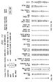
- the outer most row (row 0) on the gird has a maximum potential of 68 ball sites with 6 balls being depopulated on each of the four sides of the outermost row, resulting in a total number of 44 balls remaining for row 0.
- the next row in on the grid (row 1) has a maximum potential of 60 ball sites with 14 balls being depopulated on each of the four sides of the row, resulting in a total number of 4 balls remaining for row 1.
- the next row in on the grid (row 2) has a maximum potential of 52 ball sites with 0 balls being depopulated on each of the four sides of the row, resulting in a total number of 52 balls remaining on row 2.
- the next row in on the grid (row 3) has a maximum potential of 44 ball sites with 0 balls being depopulated on each of the four sides of the row, resulting in a total number of 44 balls remaining on row 3.
- the next row in on the grid (row 4) has a maximum potential of 36 ball sites with 7 balls being depopulated on each of the four sides of the row, resulting in a total number of 44 balls remaining on row 3. No additional rows of ball were selected. Adding all of the balls together results in a package having a footprint with 152 balls (reduced to 151 balls when the ball in the lower left had corner of row 0 is depopulated), as can be seen in Figure 7, which illustrates the results of the selection for this footprint.
- the 151 balls actually selected are not the maximum or minimum that can be obtained for a 10x10 mm package using the selective depopulation of the present teaching. Nevertheless, 151 balls is substantially more than can be obtained on a 10x10 mm package using conventional footprint design techniques requiring the optimum 280 um via size.
- Figure 8 illustrates a routing pattern of a portion of the footprint of Figure 6 along section lines 1-1. The spreadsheet indicates in fact that up to 248 balls could be routed with 280um vias if required (by depopulating on rows 0-5, 6,5,4,2,1 and 1 balls respectively).
- Figure 9 illustrates another footprint (41), with selective ball depopulation. More specifically, the selective ball depopulated footprint (41) shown in Figure 9 is a footprint for the TI 240 GHZ uStarBGA TM, package, which comprises 240 balls on a 10x10 mm body (40).
- the TI 240 GHZ uStarBGA TM, package modeling began with the selection of a 10x10 mm body (based upon combination of size of die and size limitation request of customer). Next a ball grid matrix of 17 (17x17) was selected.
- the outer most row (row 0) on the gird has a maximum potential of 64 ball sites with 3 balls being depopulated on each of the four sides of the outermost row, resulting in a total number of 52 balls remaining for row 0.
- the next row in on the grid (row 1) has a maximum potential of 56 ball sites with 2 balls being depopulated on each of the four sides of the row, resulting in a total number of 48 balls remaining for row 1.
- the next row in on the grid (row 2) has a maximum potential of 48 ball sites with 2 balls being depopulated on each of the four sides of the row, resulting in a total number of 40 balls remaining on row 2.
- the next row in on the grid (row 3) has a maximum potential of 40 ball sites with 1 ball being depopulated on each of the four sides of the row, resulting in a total number of 36 balls remaining on row 3.
- the next row in on the grid (row 4) has a maximum potential of 32 ball sites with 0 balls being depopulated on each of the four sides of the row, resulting in a total number of 32 balls remaining on row 4.
- the next row in on the grid (row 5) has a maximum potential of 24 ball sites with 0 balls being depopulated on each of the four sides of the row, resulting in a total number of 24 balls remaining on row 5.
- the next row in on the grid (row 6) has a maximum potential of 16 ball sites with 4 balls being depopulated on each of the four sides of the row, resulting in a total number of 0 balls remaining on row 6.
- the next row in on the grid (row 7) has a maximum potential of 8 ball sites with 0 balls being depopulated on each of the four sides of the row, resulting in a total number of 8 balls remaining on row 7. No additional rows of ball were selected. Adding all of the balls together results in a package having a footprint with 240 balls, as can be seen in Figure 10, which illustrates the results of the selection for this footprint.
- the 240 balls actually selected are not the maximum or minimum that can be obtained for a 10x10 mm package using the selective depopulation of the present teaching. As above, 240 balls is substantially more than can be obtained on a 10x10 mm package using conventional footprint design techniques requiring the optimum 280 um via size.
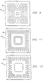
- Figure 11 illustrates yet another footprint (43), with selective ball depopulation. More specifically, the selective ball depopulated footprint (43) shown in Figure 11 is a footprint for the TI 288 GZG uStarBGA TM, package, which comprises 288 balls on a 12x12 mm body (45).
- the TI 288 GZG uStarBGA TM, package modeling began with the selection of a 12x12 mm body (based upon combination of size of die and size limitation request of customer). Next a ball grid matrix of 21 (21x21) was selected.
- the outer most row (row 0) on the gird has a maximum potential of 80 ball sites with 8 balls being depopulated on each of the four sides of the outermost row, resulting in a total number of 48 balls remaining for row 0.
- the next row in on the grid (row 1) has a maximum potential of 72 ball sites with 1 ball being depopulated on each of the four sides of the row, resulting in a total number of 68 balls remaining for row 1.
- the next row in on the grid (row 2) has a maximum potential of 64 ball sites with 0 balls being depopulated on each of the four sides of the row, resulting in a total number of 64 balls remaining on row 2.
- the next row in on the grid (row 3) has a maximum potential of 56 ball sites with 0 balls being depopulated on each of the four sides of the row, resulting in a total number of 56 balls remaining on row 3.
- the next row in on the grid (row 4) has a maximum potential of 48 ball sites with 12 balls being depopulated on each of the four sides of the row, resulting in a total number of 0 balls remaining on row 4.
- the next row in on the grid (row 5) has a maximum potential of 40 ball sites with 10 balls being depopulated on each of the four sides of the row, resulting in a total number of 0 balls remaining on row 5.
- the next row in on the grid (row 6) has a maximum potential of 32 ball sites with 1 ball being depopulated on each of the four sides of the row, resulting in a total number of 28 balls remaining on row 6.
- the next row in on the grid (row 7) has a maximum potential of 24 ball sites with 0 balls being depopulated on each of the four sides of the row, resulting in a total number of 24 balls remaining on row 7.
- the next row in on the grid (row 8) has a maximum potential of 16 ball sites with 4 balls being depopulated on each of the four sides of the row, resulting in a total number of 0 balls remaining on row 8.
- the next row in on the grid (row 9) has a maximum potential of 8 ball sites with 2 balls being depopulated on each of the four sides of the row, resulting in a total number of 0 balls remaining on row 9. No additional rows of ball were selected.
- Adding all of the balls together results in a package having a footprint with 288 balls, as can be seen in Figure 12, which illustrates the results of the selection for this footprint.
- the 288 balls actually selected are not the maximum or minimum that can be obtained for a 12x12 mm package using the selective depopulation of the present teaching. As above, 288 balls is substantially more than can be obtained on a 12x12 mm package using conventional footprint design techniques requiring the optimum 280 um via size.
- Figure 13 illustrates still another footprint (47), with selective ball depopulation. More specifically, the selective ball depopulated footprint (47) shown in Figure 11 is a footprint for the TI 240 GZG uStarBGA TM, package, which comprises 240 balls on a 12x12 mm body (45).
- the TI 240 GZG uStarBGA TM, package modeling began with the selection of a 12x12 mm body (based upon combination of size of die and size limitation request of customer). Next a ball grid matrix of 21 (21x21) was selected.
- the outer most row (row 0) on the gird has a maximum potential of 80 ball sites with 8 balls being depopulated on each of the four sides of the outermost row, resulting in a total number of 48 balls remaining for row 0.
- the next row in on the grid (row 1) has a maximum potential of 72 ball sites with 1 ball being depopulated on each of the four sides of the row, resulting in a total number of 68 balls remaining for row 1.
- the next row in on the grid (row 2) has a maximum potential of 64 ball sites with 2 balls being depopulated on each of the four sides of the row, resulting in a total number of 56 balls remaining on row 2.
- the next row in on the grid (row 3) has a maximum potential of 56 ball sites with 4 balls being depopulated on each of the four sides of the row, resulting in a total number of 40 balls remaining on row 3.
- the next row in on the grid (row 4) has a maximum potential of 48 ball sites with 12 balls being depopulated on each of the four sides of the row, resulting in a total number of 0 balls remaining on row 4.
- the next row in on the grid (row 5) has a maximum potential of 40 ball sites with 10 balls being depopulated on each of the four sides of the row, resulting in a total number of 0 balls remaining on row 5.
- the next row in on the grid (row 6) has a maximum potential of 32 ball sites with 1 ball being depopulated on each of the four sides of the row, resulting in a total number of 28 balls remaining on row 6.
- the next row in on the grid (row 7) has a maximum potential of 24 ball sites with 6 balls being depopulated on each of the four sides of the row, resulting in a total number of 0 balls remaining on row 7.
- the next row in on the grid (row 8) has a maximum potential of 16 ball sites with 4 balls being depopulated on each of the four sides of the row, resulting in a total number of 0 balls remaining on row 8.
- the next row in on the grid (row 9) has a maximum potential of 8 ball sites with 2 balls being depopulated on each of the four sides of the row, resulting in a total number of 0 balls remaining on row 9. No additional rows of ball were selected.
- Adding all of the balls together results in a package having a footprint with 240 balls, as can be seen in Figure 14, which illustrates the results of the selection for this footprint.
- the 240 balls actually selected are not the maximum or minimum that can be obtained for a 12x12 mm package using the selective depopulation of the present teaching. As above, 240 balls is substantially more than can be obtained on a 12x12 mm package using conventional footprint design techniques requiring the optimum 280 um via size.
- Figure 15 illustrates still yet another footprint (49), with selective ball depopulation. More specifically, the selective ball depopulated footprint (49) shown in Figure 15 is a footprint for the TI 256 GZG uStarBGA TM, package, which comprises 256 balls on a 12x12 mm body (45).
- the TI 256 GZG uStarBGA TM, package modeling began with the selection of a 12x12 mm body (based upon combination of size of die and size limitation request of customer). Next a ball grid matrix of 21 (21x21) was selected.
- the outer most row (row 0) on the gird has a maximum potential of 80 ball sites with 8 balls being depopulated on each of the four sides of the outermost row, resulting in a total number of 48 balls remaining for row 0.
- the next row in on the grid (row 1) has a maximum potential of 72 ball sites with 1 ball being depopulated on each of the four sides of the row, resulting in a total number of 68 balls remaining for row 1.
- the next row in on the grid (row 2) has a maximum potential of 64 ball sites with 0 balls being depopulated on each of the four sides of the row, resulting in a total number of 64 balls remaining on row 2.
- the next row in on the grid (row 3) has a maximum potential of 56 ball sites with 2 balls being depopulated on each of the four sides of the row, resulting in a total number of 48 balls remaining on row 3.
- the next row in on the grid (row 4) has a maximum potential of 48 ball sites with 12 balls being depopulated on each of the four sides of the row, resulting in a total number of 0 balls remaining on row 4.
- the next row in on the grid (row 5) has a maximum potential of 40 ball sites with 10 balls being depopulated on each of the four sides of the row, resulting in a total number of 0 balls remaining on row 5.
- the next row in on the grid (row 6) has a maximum potential of 32 ball sites with 1 ball being depopulated on each of the four sides of the row, resulting in a total number of 28 balls remaining on row 6.
- the next row in on the grid (row 7) has a maximum potential of 24 ball sites with 6 balls being depopulated on each of the four sides of the row, resulting in a total number of 0 balls remaining on row 7.
- the next row in on the grid (row 8) has a maximum potential of 16 ball sites with 4 balls being depopulated on each of the four sides of the row, resulting in a total number of 0 balls remaining on row 8.
- the next row in on the grid (row 9) has a maximum potential of 8 ball sites with 2 balls being depopulated on each of the four sides of the row, resulting in a total number of 0 balls remaining on row 9. No additional rows of ball were selected.
- Adding all of the balls together results in a package having a footprint with 256 balls, as can be seen in Figure 16, which illustrates the results of the selection for this footprint.
- the 256 balls actually selected are not the maximum or minimum that can be obtained for a 12x12 mm package using the selective depopulation of the present teaching. As above, 256 balls is substantially more than can be obtained on a 12x12 mm package using conventional footprint design techniques requiring the optimum 280 um via size.
- Table 1 shows the results of the board level reliability (BLR) tests done on both the conventional and 'smart footprints'. Due to the heavy dependence of die size on reliability, the die in both cases was kept constant (6.0x6.0mm). In order to focus on the package reliability, only failures in the package side of the joint are reported: Board level reliability of conventional and 'Smart-Foot'TM packages. Via Diameter (mm) Sample Size Cycles to first failure Conventional Footprint 0.212 28 550 'Smart-Foot'TM Footprint 0.280 31 1450
- the ability to model proposed solutions is invaluable in bringing new packages to market quickly.
- the TI 151 CSP 'Smart-Foot'TM packages was modeled using a two-dimensional finite element analysis tool before any new tooling was committed. The model confirmed the proposed reliability benefit in advance.
- the 151 ball CSP 'Smart-Foot'TM package not only proved as reliable as the model predicted, but all reliability tests passed first time.
- Figure 13 shows the worst case elastic strain prediction for both packages as a function of die size, and clearly shows a much lower strain in the case of the 'Smart-Foot'TM package.
- the 144 TQFP package has been a high running package for these applications.
- the 0.50mm pitch version with a 10x10mm body size needed to be developed.
- a software-controlled programmable processing device such as a Digital Signal Processor, microprocessor, other processing devices, data processing apparatus or computer system
- a computer program for configuring a programmable device, apparatus or system to implement the foregoing described modelling techniques is envisaged as an aspect of the present invention.
- the computer program may be embodied as source code and undergo compilation for implementation on a processing device, apparatus or system, or may be embodied as object code.
- object code The skilled person would readily understand that the term computer in its most general sense encompasses programmable devices such as referred to above, and data processing apparatus and computer systems.
- the computer program is stored on a carrier medium in machine or device readable form, for example in solid-state memory or magnetic memory such as disc or tape and the processing device utilises the program or a part thereof to configure it for operation.
- the computer program may be supplied from a remote source embodied in a communications medium such as an electronic signal, radio frequency carrier wave or optical carrier wave.
- a communications medium such as an electronic signal, radio frequency carrier wave or optical carrier wave.
- carrier media are also envisaged as aspects of the present invention.
Abstract
Description
- The present invention relates to the field of integrated circuit devices. More specifically, but not exclusively, the present invention relates to a modeling technique for selectively depopulating electrical contacts from a foot print of a grid array (ball grid array (BGA) or land grid array (LGA)) package to increase the routability of the package substrate and increase the device reliability.
- The parallel drive towards total cost reduction and miniaturization has, in recent years, given rise to an increasing emphasis on very small IC package solutions. This is particularly evident in consumer based end equipment such as camcorders and mobile telephone handsets. Despite a formal definition, packages whose area is similar to that of the IC they encapsulate are loosely referred to as chip scale packages (CSPs).
- CSPs are in many ways an ideal solution to the cost reduction and miniaturization requirement. They offer enormous area reductions compared with quad flat package, and have increasing potential to do so without adding system level cost. In the best case, CSPs are able to compete today, on a cost per terminal basis, with quad flat packages. For example, various CSPs from Texas Instruments are now available at cost parity with thin quad flat packages.
- Texas Instruments produces a polyimide-based family of CSPs known as MicroStarBGA™ (see Figure 1) . This CSP 10, like most others, uses
solder alloy balls 12 as the interconnection between thepackage substrate 14 and the board on which the packages is soldered. As with all such packages, the solder balls formed between the package and the board are susceptible to fatigue when exposed to cyclic ambient temperature conditions. - JEDEC and EIAJ are increasingly documenting fine pitch BGA industry standards. The finest pitch standard that is currently widely recognized is 0.50mm pitch. However, broad acceptance and use of 0.50mm pitch CSPs is still very limited, due to the following reasons:
- 1) Lack of package availability from a broad range of suppliers.
- 2) Lack of package reliability data, and concerns that reliability will not meet the requirements of even the consumer markets.
- 3) The printed circuit board (PCB) requirements for mounting such fine pitch packages are very demanding. There is limited availability of such boards, and in many cases, the higher PCB cost is prohibitive.
- 4) Lack of experience on the part of most SMT assembly operations in manufacturing with such fine pitch BGAs.
- 5) Belief that 0.50mm pitch CSP component cost is inherently higher, on a cost per terminal basis, than for example, 0.80mm pitch CSPs.
-
- Clearly, key to the successful adoption of a package that has to meet the twin goals of system cost reduction and miniaturization, is the package reliability. As the ball pitch shrinks, it becomes more and more difficult to meet reliability specifications, due to the ball joint fatigue phenomenon mentioned in the introduction. Both the size (volume) and shape of the solder ball influence reliability. The weakest link in the system is normally the point of smallest cross-section in the solder joint, which is via (28), as seen in Figure 2.
- Thus a major challenge in the design of the CSP substrate is to optimize the diameter of this solder via. However, as the ball density on the package increases (more balls on more rows, at finer pitch), substrate routing density also increases, often leading to a package design of inherent lower reliability. To demonstrate this, the current optimum design for reliability, as shown in Figure 3, is:
- Ball (12) pitch
- : 500 um
- Line (30)/Space
- : 28/42 um
- Via (32) diameter
- : 280 um
- Solder ball pad (34) diameter
- : 380 um
- These optimum rules, based on design for reliability, allow only one trace or line (30) to pass between adjacent balls (12). This is important since in CSP packages, since a line or trace (30) must extend from each solder ball pad (34) to an exterior edge of the substrate (14) (e.g., to facilitate electrolytic plating). Such restriction of limiting one line or trace between adjacent balls will limit the total number of balls that may actually be implemented in a matrix type ball grid array since there will be a limitation on how many traces or lines may actually extend out to an exterior surface of the substrate.
- Figure 4 discloses a conventional ball footprint (regular pattern of 3 row of balls) having 144 balls (on a 0.5 mm pitch) on a 10x10mm package body. To achieve this dense routing, a designer has to compromise. There are typically three options:
- 1) Tighten the line/space design rule for the connection traces. This can add cost or may be beyond the capability of the substrate technology.
- 2) Reduce the via diameter. This will reduce the fatigue life of the solder joint.
- 3) Reduce the minimum overlap of the ball pad to via (see Figure
- 4). This has negative reliability implications, as it will effect the moisture sensitivity of the package.
-
- Figure 5 discloses a routing pattern for 3 full rows of balls, in which:
- Ball (12) pitch
- : 500 um
- Line (30) / Space
- : 28/42 um
- Via (32) diameter
- : 218 um
- Solder ball pad (34) diameter
- : 318 um
- Thus, in the case of Figure 4 (and by implication Figure 5), the designer chose
option 2. In order to allow two traces to route between adjacent balls, the via diameter had to be reduced from 280 um to 218 um, which is a violation of the optimum design rules which call for a via diameter of 280 um. There are significant reliability implications of such a modification or change, as is well known in the art. - An embodiment of the invention provides a modeling technique for selectively depopulating solder contacts (and their respective contact pads, vias and traces or lines) from a conventional foot print of a grid array package (Ball Grid Array (BGA), or Land Grid Array (LGA)) to improve device reliability, and a BGA or LGA package so modeled. The modeling technique anticipates a routing of traces through the gap resulting from the depopulated solder contacts as additional space for routing traces or lines from solder contact pads to an exterior surface of a substrate (14) upon which a semiconductor die (20) is mounted. An advantage of an embodiment of the present invention is that it provides an easy to use modeling technique (e.g., in this case an Excel spreadsheet) that allows a user to easily predict whether or not a preselected number of balls on a specific body size device will be possible.
- Features believed characteristic of the invention are set forth in the appended claims. Embodiments of the invention itself, however, as well as other features and advantages thereof, will be best understood by reference to the detailed description which follows, read in conjunction with the accompanying drawings, wherein:
- Figure 1 is an exploded sectional view of a ball grid array (BGA) package.
- Figure 2 is a cross sectional view of a ball grid array (BGA) package mounted on a printed wiring board (PWB).
- Figure 3 illustrates the current optimum design for vias, solder ball pads and traces or lines.
- Figure 4 illustrates a conventional ball grid array footprint that can be attained when current optimum design rules are compromised.
- Figure 5 illustrates a routing pattern for three full rows of balls in the ball grid array footprint of Figure 4.
- Figure 6 illustrates a ball grid array footprint with selective ball depopulation, according to one embodiment of the invention.
- Figure 7 illustrates the modeling results for the ball grid array footprint of Figures 5 and 6.
- Figure 8 illustrates a routing pattern of a portion of the footprint of Figure 6.
- Figure 9 illustrates a ball grid array footprint with selective ball depopulation, according to another embodiment of the invention.
- Figure 10 illustrates the modeling results for the ball grid array footprint of Figure 9.
- Figure 11 illustrates a ball grid array footprint with selective ball depopulation, according to yet another embodiment of the invention.
- Figure 12 illustrates the modeling results for the ball grid array footprint of Figure 11.
- Figure 13 illustrates a ball grid array footprint with selective ball depopulation, according to still another embodiment of the invention.
- Figure 14 illustrates the modeling results for the ball grid array footprint of Figure 13.
- Figure 15 illustrates a ball grid array footprint with selective ball depopulation, according to still yet another embodiment of the invention.
- Figure 16 illustrates the modeling results for the ball grid array footprint of Figure 15.
- Figure 17 illustrates a worst case elastic strain prediction for conventional ball grid array and selectively depopulated ball grid array packages as a function of die size.
-
- Taking a radical look at footprint design, it is possible to overcome many of the restrictions and compromises discussed above. Using the principle of selective ball depopulation, it is possible to return to the optimum design rule for reliability and match the ball density of the conventional footprint design. However, the complexity of the footprint design has now increased significantly, especially as (as far as the author is aware) there are no available software design tools available today to handle this.
- As shown in Figure 3, a 280 um via (32) only permits one trace between adjacent balls (12). If however, we depopulate a ball (including its associated via (32), solder ball pad (34) and trace or line (30)), we can now place up to 8 traces or lines (30) when using the 25um rule-line/
space 28/42 (or up to 13 traces or lines (30) when using the 18um rule-line/space 20/30 - these numbers will change when other rule-line/space numbers are selected) in the resulting gap between 2 adjacent balls. By careful selection of these depopulated balls, it is possible to route as many, if not more total balls with the optimum design rule (optimum via diameter), as compared to the conventional footprint with compromised design rules (e.g., via diameter of less than 280 um) . This design concept is called 'Smart-Foot'™, . - Figure 6 illustrates a footprint (38), with selective ball depopulation. More specifically, the selective ball depopulated footprint (38) shown in Figure 6 is a footprint for the
TI 151 GHZ uStarBGA ™, package, which comprises 151 balls on a 10x10 mm body (40). Figure 7 discloses an Excel spreadsheet incorporating a modeling technique that allows a package designer to quickly determine whether or not a preselected number of balls for a specific body size is feasible. In order for the modeling technique to work, there are some parameter that have to be preselected (or inserted into the spreadsheet's calculation rules) and others that can be entered "on the fly" by a designer. For example, in the case of Figure 7, a 0.50mm pitch is preselected which is the largest possible matrix with n-1 row depopulated. A Viacap rule of 50 um is also preselected which is an overlap of metal from the edge of the via. The body size parameter is one which a designer next selects "on the fly" (10mm in the case of Figure 7). The matrix parameter is also selected "on the fly" (18 in the case of Figure 7). The Ball Pitch is preselected (500um in the case of Figure 7). Next, there are 17 vertical columns of information that must be filled in - most preselected, but a few "on the fly". -
Column 1 is the "Row n-" column. It lists at least the total number of possible rows (four-sided) for the selected body size, starting with "row 0" as the outer most (and therefore largest) row and working up to "row n" as the inner most (and therefore smallest row). While 11 rows are listed (0-10), 9 are the most available in the case of Figure 7. The total number of rows is preselected and will vary depending upon body size and matrix selected. -
Column 2 is the "Ballsites/row" column.Column 2 lists the total possible number of ball sites available for each specific row. While the number for each row is initially preselected, the program will automatically change the numbers as the body and matrix number are changed "on the fly" by a designer. In the case of Figure 7 (10mm body size and matrix of 18),row 0 lists 68 ball sites available. Each additional row lists a correspondingly reduced number of ball sites untilrow 8, which lists 4 ball sites available. Being that the spreadsheet was designed with substrate design rules in mind (knowledge available to one of ordinary skill in the art), these numbers are changed by the spreadsheet and not by a device designer. -
Column 3 is the "Balls depopulated per side" of a four-sided row. These are selected by a designer "on the fly". A designer can select from 0 to a full 1/4 of the total number of ball sites, to depopulate on each row. -
Column 4 is the "Remaining balls on row" column which lists the total number of balls remaining in the respective four-sided row. While these numbers will be initially preselected to be the same as their respective "ballsites/row" assuming 0 balls depopulated per side, the spreadsheet will automatically change the numbers as a designer changes the numbers inColumn 3 "on the fly". -
Column 5 is the "Number of reduced size vias/Side". The numbers in this column are preselected by a designer should be 0 for each row having standard size vias. This number is preset by the design rules and will not change unless the designer prechooses a nonstandard via size. -
Column 6 is the "Standard via size (um)" column. The numbers in this column are preselected by a designer and, currently, standards bodies have selected 280 um as being a standard size. This will not change unless the designer preselects another standard size. -
Column 8 is the "Reduced via size (um)" column. The numbers in this column are preselected by a designer and, if reduced vias are to be used in conjunction with standard size vias, then the designer must prechoose the reduced size. If no reduced size vias are to be selected, then the number should be left the same as inColumn 7. -
Column 9 is the "Line width (um)" column. The numbers in this column are preselected by a designer and, if the 18um copper rule is selected, the number placed in each row ofcolumn 9 is 18. If by change the 25 um copper rule is selected, 28 is the number placed in each row ofcolumn 9. While the current invention contemplates two rules to choose from, e.g., the 18 um and 25 um rules for line/space, other can also be used. -
Column 10 is the "Space width (um)" column. The numbers in this column are preselected by a designer and, if the 18 um copper rule is selected, the number placed in each row ofcolumn 10 is 28. If, on the other hand, the 25 um copper rule is selected, 42 is the number placed in each row ofcolumn 10. While the current invention contemplates two rules to choose from, e.g., the 18 um and 25 um rules for line/space, other can also be used. -
Column 11 is the "Traces between standard vias" column. The numbers in this column are preselected by a designer and, under currently accepted industry standards, if the 18um line/space rule is selected, 2 is preselected and placed in each row ofcolumn 11. If, on the other hand, the 25um line/space rule is selected, 1 is preselected and placed in each row ofcolumn 11. As above, this number may change for other line/spacing rules or as industry standards change. -
Column 12 is the "Traces per depopulated ball" column. The numbers in this column are preselected by a designer and, under currently accepted industry spacing standards, if the 18um rule is selected, up to 12 traces per depopulated ball are possible. If the 25um line/spacing rule is selected, up to 8 traces per depopulated ball are possible. As above, this number may change for other line/spacing rules or as industry standards change. - Column 13 is the "Max traces (balls inside) column. This calculates the total number of metal traces that can be placed between the balls (with or without depopulation) on the given row. This equates to the maximum number of balls that can be placed on the sum of all the rows inside the given row.
-
Column 14 is the "Max Traces OK?" column. This checks that the number of allowable traces between the balls on the given column is sufficient to accommodate all the balls currently specified as present on the sum of the rows inside the given row. If not, a warning value of -99999 is calculated, resulting in a non-workable solution. If this non-workable solution is flagged, then more balls can be depopulated incolumn 3 until a workable solution is found. - Column 15 is the "Total Possible Balls" column. This shows the number of balls on the given row, if the result in
column 14 is workable. If not, it shows the value zero, and subsequently indicates a non-workable total (zero) in the "TOTAL" cell. -
Column 16 is the "Actual Balls Inside" column. This shows the total number of balls currently present inside the given row. This is compared to the theoretical maximum balls possible shown in column 13. If the actual is less than the theoretical maximum, this indicates a workable solution, and is used to calculate the difference between theoretical and actual incolumn 17. -
Column 17 is the "Delta" column. This calculates the difference between the actual balls inside the given row, and the theoretical maximum number of balls possible inside the given row. The closer to zero, the more difficult the routing is likely to be. - Once all of the "preselected" parameters have been entered into the spreadsheet, a designer is free to enter and change numbers "on the fly" in the "Body", "Matrix" and "Balls depopulated per side (col. 3)", in order to predict the feasibility of the ball grid pattern selected by the designer. If a positive number comes up for the Total number of balls, then the pattern selected by the designer is possible. If, however, a "0" comes up for the Total number of balls, then the pattern selected by the designer is not possible using the preselected design parameters.
- Referring back to Figure 7, modeling for the
TI 151 GHZ uStarBGA ™, package began with the selection of a 10x10 mm body (based upon combination of size of die and size limitation request of customer). Next a ball grid matrix of 18 (18x18) was selected. Recall from the previous discussions that it is not possible to utilize a full 18x18 ball grid array having 324 balls (or any other grid of substantial size for that matter), using optimum design rules, since a trace or line for each viable die pad must extend to the outer surface of the substrate and there is not enough room between all of the .28 mm diameter vias to accommodate all of the traces. The trick is to intelligently decide which balls to depopulate in order to arrive at the desired footprint. So, in the embodiment of Figures 6 and 8, a standard size via of 280 um, a line width of 28 um - which allows one trace between standard vias and up to 8 traces between two vias having a depopulated via spaced therebetween. - Using the above criteria, the outer most row (row 0) on the gird (having four identical sides) has a maximum potential of 68 ball sites with 6 balls being depopulated on each of the four sides of the outermost row, resulting in a total number of 44 balls remaining for
row 0. The next row in on the grid (row 1) has a maximum potential of 60 ball sites with 14 balls being depopulated on each of the four sides of the row, resulting in a total number of 4 balls remaining forrow 1. The next row in on the grid (row 2) has a maximum potential of 52 ball sites with 0 balls being depopulated on each of the four sides of the row, resulting in a total number of 52 balls remaining onrow 2. The next row in on the grid (row 3) has a maximum potential of 44 ball sites with 0 balls being depopulated on each of the four sides of the row, resulting in a total number of 44 balls remaining onrow 3. The next row in on the grid (row 4) has a maximum potential of 36 ball sites with 7 balls being depopulated on each of the four sides of the row, resulting in a total number of 44 balls remaining onrow 3. No additional rows of ball were selected. Adding all of the balls together results in a package having a footprint with 152 balls (reduced to 151 balls when the ball in the lower left had corner ofrow 0 is depopulated), as can be seen in Figure 7, which illustrates the results of the selection for this footprint. In this example, the 151 balls actually selected are not the maximum or minimum that can be obtained for a 10x10 mm package using the selective depopulation of the present teaching. Nevertheless, 151 balls is substantially more than can be obtained on a 10x10 mm package using conventional footprint design techniques requiring the optimum 280 um via size. Figure 8 illustrates a routing pattern of a portion of the footprint of Figure 6 along section lines 1-1. The spreadsheet indicates in fact that up to 248 balls could be routed with 280um vias if required (by depopulating on rows 0-5, 6,5,4,2,1 and 1 balls respectively). - Figure 9 illustrates another footprint (41), with selective ball depopulation. More specifically, the selective ball depopulated footprint (41) shown in Figure 9 is a footprint for the
TI 240 GHZ uStarBGA ™, package, which comprises 240 balls on a 10x10 mm body (40). TheTI 240 GHZ uStarBGA ™, package modeling began with the selection of a 10x10 mm body (based upon combination of size of die and size limitation request of customer). Next a ball grid matrix of 17 (17x17) was selected. In the embodiment of Figure 9, a standard size via of 280 um, a line width of 18 um (less than current optimum design rules) - which allows two traces between standard vias and up to 12 traces between two vias having a depopulated via spaced therebetween. - Using the above criteria, the outer most row (row 0) on the gird (having four identical sides) has a maximum potential of 64 ball sites with 3 balls being depopulated on each of the four sides of the outermost row, resulting in a total number of 52 balls remaining for
row 0. The next row in on the grid (row 1) has a maximum potential of 56 ball sites with 2 balls being depopulated on each of the four sides of the row, resulting in a total number of 48 balls remaining forrow 1. The next row in on the grid (row 2) has a maximum potential of 48 ball sites with 2 balls being depopulated on each of the four sides of the row, resulting in a total number of 40 balls remaining onrow 2. The next row in on the grid (row 3) has a maximum potential of 40 ball sites with 1 ball being depopulated on each of the four sides of the row, resulting in a total number of 36 balls remaining onrow 3. The next row in on the grid (row 4) has a maximum potential of 32 ball sites with 0 balls being depopulated on each of the four sides of the row, resulting in a total number of 32 balls remaining onrow 4. The next row in on the grid (row 5) has a maximum potential of 24 ball sites with 0 balls being depopulated on each of the four sides of the row, resulting in a total number of 24 balls remaining onrow 5. The next row in on the grid (row 6) has a maximum potential of 16 ball sites with 4 balls being depopulated on each of the four sides of the row, resulting in a total number of 0 balls remaining onrow 6. The next row in on the grid (row 7) has a maximum potential of 8 ball sites with 0 balls being depopulated on each of the four sides of the row, resulting in a total number of 8 balls remaining onrow 7. No additional rows of ball were selected. Adding all of the balls together results in a package having a footprint with 240 balls, as can be seen in Figure 10, which illustrates the results of the selection for this footprint. As the above-described 151 ball footprint example, the 240 balls actually selected are not the maximum or minimum that can be obtained for a 10x10 mm package using the selective depopulation of the present teaching. As above, 240 balls is substantially more than can be obtained on a 10x10 mm package using conventional footprint design techniques requiring the optimum 280 um via size. - Figure 11 illustrates yet another footprint (43), with selective ball depopulation. More specifically, the selective ball depopulated footprint (43) shown in Figure 11 is a footprint for the
TI 288 GZG uStarBGA ™, package, which comprises 288 balls on a 12x12 mm body (45). TheTI 288 GZG uStarBGA ™, package modeling began with the selection of a 12x12 mm body (based upon combination of size of die and size limitation request of customer). Next a ball grid matrix of 21 (21x21) was selected. In the embodiment of Figure 11, a standard size via of 280 um, a line width of 18 um (less than current optimum design rules) - which allows two traces between standard vias and up to 12 traces between two vias having a depopulated via spaced therebetween. - Using the above criteria, the outer most row (row 0) on the gird (having four identical sides) has a maximum potential of 80 ball sites with 8 balls being depopulated on each of the four sides of the outermost row, resulting in a total number of 48 balls remaining for
row 0. The next row in on the grid (row 1) has a maximum potential of 72 ball sites with 1 ball being depopulated on each of the four sides of the row, resulting in a total number of 68 balls remaining forrow 1. The next row in on the grid (row 2) has a maximum potential of 64 ball sites with 0 balls being depopulated on each of the four sides of the row, resulting in a total number of 64 balls remaining onrow 2. The next row in on the grid (row 3) has a maximum potential of 56 ball sites with 0 balls being depopulated on each of the four sides of the row, resulting in a total number of 56 balls remaining onrow 3. The next row in on the grid (row 4) has a maximum potential of 48 ball sites with 12 balls being depopulated on each of the four sides of the row, resulting in a total number of 0 balls remaining onrow 4. The next row in on the grid (row 5) has a maximum potential of 40 ball sites with 10 balls being depopulated on each of the four sides of the row, resulting in a total number of 0 balls remaining onrow 5. The next row in on the grid (row 6) has a maximum potential of 32 ball sites with 1 ball being depopulated on each of the four sides of the row, resulting in a total number of 28 balls remaining onrow 6. The next row in on the grid (row 7) has a maximum potential of 24 ball sites with 0 balls being depopulated on each of the four sides of the row, resulting in a total number of 24 balls remaining onrow 7. The next row in on the grid (row 8) has a maximum potential of 16 ball sites with 4 balls being depopulated on each of the four sides of the row, resulting in a total number of 0 balls remaining onrow 8. The next row in on the grid (row 9) has a maximum potential of 8 ball sites with 2 balls being depopulated on each of the four sides of the row, resulting in a total number of 0 balls remaining onrow 9. No additional rows of ball were selected. Adding all of the balls together results in a package having a footprint with 288 balls, as can be seen in Figure 12, which illustrates the results of the selection for this footprint. The 288 balls actually selected are not the maximum or minimum that can be obtained for a 12x12 mm package using the selective depopulation of the present teaching. As above, 288 balls is substantially more than can be obtained on a 12x12 mm package using conventional footprint design techniques requiring the optimum 280 um via size. - Figure 13 illustrates still another footprint (47), with selective ball depopulation. More specifically, the selective ball depopulated footprint (47) shown in Figure 11 is a footprint for the
TI 240 GZG uStarBGA ™, package, which comprises 240 balls on a 12x12 mm body (45). TheTI 240 GZG uStarBGA ™, package modeling began with the selection of a 12x12 mm body (based upon combination of size of die and size limitation request of customer). Next a ball grid matrix of 21 (21x21) was selected. In the embodiment of Figure 13, a standard size via of 280 um, a line width of 18 um (less than current optimum design rules) - which allows two traces between standard vias and up to 12 traces between two vias having a depopulated via spaced therebetween. - Using the above criteria, the outer most row (row 0) on the gird (having four identical sides) has a maximum potential of 80 ball sites with 8 balls being depopulated on each of the four sides of the outermost row, resulting in a total number of 48 balls remaining for
row 0. The next row in on the grid (row 1) has a maximum potential of 72 ball sites with 1 ball being depopulated on each of the four sides of the row, resulting in a total number of 68 balls remaining forrow 1. The next row in on the grid (row 2) has a maximum potential of 64 ball sites with 2 balls being depopulated on each of the four sides of the row, resulting in a total number of 56 balls remaining onrow 2. The next row in on the grid (row 3) has a maximum potential of 56 ball sites with 4 balls being depopulated on each of the four sides of the row, resulting in a total number of 40 balls remaining onrow 3. The next row in on the grid (row 4) has a maximum potential of 48 ball sites with 12 balls being depopulated on each of the four sides of the row, resulting in a total number of 0 balls remaining onrow 4. The next row in on the grid (row 5) has a maximum potential of 40 ball sites with 10 balls being depopulated on each of the four sides of the row, resulting in a total number of 0 balls remaining onrow 5. The next row in on the grid (row 6) has a maximum potential of 32 ball sites with 1 ball being depopulated on each of the four sides of the row, resulting in a total number of 28 balls remaining onrow 6. The next row in on the grid (row 7) has a maximum potential of 24 ball sites with 6 balls being depopulated on each of the four sides of the row, resulting in a total number of 0 balls remaining onrow 7. The next row in on the grid (row 8) has a maximum potential of 16 ball sites with 4 balls being depopulated on each of the four sides of the row, resulting in a total number of 0 balls remaining onrow 8. The next row in on the grid (row 9) has a maximum potential of 8 ball sites with 2 balls being depopulated on each of the four sides of the row, resulting in a total number of 0 balls remaining onrow 9. No additional rows of ball were selected. Adding all of the balls together results in a package having a footprint with 240 balls, as can be seen in Figure 14, which illustrates the results of the selection for this footprint. The 240 balls actually selected are not the maximum or minimum that can be obtained for a 12x12 mm package using the selective depopulation of the present teaching. As above, 240 balls is substantially more than can be obtained on a 12x12 mm package using conventional footprint design techniques requiring the optimum 280 um via size. - Figure 15 illustrates still yet another footprint (49), with selective ball depopulation. More specifically, the selective ball depopulated footprint (49) shown in Figure 15 is a footprint for the
TI 256 GZG uStarBGA ™, package, which comprises 256 balls on a 12x12 mm body (45). TheTI 256 GZG uStarBGA ™, package modeling began with the selection of a 12x12 mm body (based upon combination of size of die and size limitation request of customer). Next a ball grid matrix of 21 (21x21) was selected. In the embodiment of Figure 15, a standard size via of 280 um, a line width of 18 um (less than current optimum design rules) - which allows two traces between standard vias and up to 12 traces between two vias having a depopulated via spaced therebetween. - Using the above criteria, the outer most row (row 0) on the gird (having four identical sides) has a maximum potential of 80 ball sites with 8 balls being depopulated on each of the four sides of the outermost row, resulting in a total number of 48 balls remaining for
row 0. The next row in on the grid (row 1) has a maximum potential of 72 ball sites with 1 ball being depopulated on each of the four sides of the row, resulting in a total number of 68 balls remaining forrow 1. The next row in on the grid (row 2) has a maximum potential of 64 ball sites with 0 balls being depopulated on each of the four sides of the row, resulting in a total number of 64 balls remaining onrow 2. The next row in on the grid (row 3) has a maximum potential of 56 ball sites with 2 balls being depopulated on each of the four sides of the row, resulting in a total number of 48 balls remaining onrow 3. The next row in on the grid (row 4) has a maximum potential of 48 ball sites with 12 balls being depopulated on each of the four sides of the row, resulting in a total number of 0 balls remaining onrow 4. The next row in on the grid (row 5) has a maximum potential of 40 ball sites with 10 balls being depopulated on each of the four sides of the row, resulting in a total number of 0 balls remaining onrow 5. The next row in on the grid (row 6) has a maximum potential of 32 ball sites with 1 ball being depopulated on each of the four sides of the row, resulting in a total number of 28 balls remaining onrow 6. The next row in on the grid (row 7) has a maximum potential of 24 ball sites with 6 balls being depopulated on each of the four sides of the row, resulting in a total number of 0 balls remaining onrow 7. The next row in on the grid (row 8) has a maximum potential of 16 ball sites with 4 balls being depopulated on each of the four sides of the row, resulting in a total number of 0 balls remaining onrow 8. The next row in on the grid (row 9) has a maximum potential of 8 ball sites with 2 balls being depopulated on each of the four sides of the row, resulting in a total number of 0 balls remaining onrow 9. No additional rows of ball were selected. Adding all of the balls together results in a package having a footprint with 256 balls, as can be seen in Figure 16, which illustrates the results of the selection for this footprint. The 256 balls actually selected are not the maximum or minimum that can be obtained for a 12x12 mm package using the selective depopulation of the present teaching. As above, 256 balls is substantially more than can be obtained on a 12x12 mm package using conventional footprint design techniques requiring the optimum 280 um via size. - Table 1 shows the results of the board level reliability (BLR) tests done on both the conventional and 'smart footprints'. Due to the heavy dependence of die size on reliability, the die in both cases was kept constant (6.0x6.0mm). In order to focus on the package reliability, only failures in the package side of the joint are reported:
Board level reliability of conventional and 'Smart-Foot'™ packages.Via Diameter (mm) Sample Size Cycles to first failure Conventional Footprint 0.212 28 550 'Smart-Foot'™ Footprint 0.280 31 1450 - Other design and test features used for this test are as follows:
- Temperature range
- : -40/125 degC
- Ramp time
- : 2-5minutes
- Dwell time
- : 11-13minutes
- Board land type
- : Copper, Ni/Au plated
- Board material
- : FR4
- Board thickness
- : 0.80mm
- Land design
- : Non-soldermask defined
- Land diameter
- : 0.20mm
- The ability to model proposed solutions is invaluable in bringing new packages to market quickly. The
TI 151 CSP 'Smart-Foot'™ packages was modeled using a two-dimensional finite element analysis tool before any new tooling was committed. The model confirmed the proposed reliability benefit in advance. The 151 ball CSP 'Smart-Foot'™ package not only proved as reliable as the model predicted, but all reliability tests passed first time. Figure 13 shows the worst case elastic strain prediction for both packages as a function of die size, and clearly shows a much lower strain in the case of the 'Smart-Foot'™ package. - Custom DSPs for wireless handsets frequently use packages with 144 contacts. The 144 TQFP package has been a high running package for these applications. As discussed in the introduction, there is a clear need to reduce the size of traditional QFP packages to equivalent chip scale packages. Thus a 144 CSP was required. A 12x12mm body 144 CSP with 0.80mm ball pitch as been developed, and has been a high running CSP since 1997. As further package shrinks were required, the 0.50mm pitch version, with a 10x10mm body size needed to be developed. Today, 10x10mm body packages with 0.50mm pitch are available with both conventional and 'Smart-Foot'™ footprints.
- As the need for smaller bodied packages continues, we will see more package designs following this innovative path. Already, 12x12mm and 13x13mm body 'Smart-Foot'™ packages are being designed for applications with higher total ball count.
- With a somewhat 'custom' approach to package design, various criticisms can be anticipated:
- 1) That 'Smart-Foot'™ packages look unconventional, and do not conform to the footprints offered by other vendors. Fortunately, due to the high volume of Wireless applications, a somewhat 'custom' footprint is easily justified in the context of the reliability benefits.
- 2) That the board routability of such unusual footprints may be a problem. Actually, there is no added system cost penalty with this approach since routing of the 'Smart-Foot'™ footprint may actually be easier because of the spread out configuration. In the case of larger packages, such as 240 and 304 balls, additional care is necessary to ensure that board routability is not degraded, but such is easily accomplished.
- 3) That package cost will be higher. Other than a longer design cycle, cost of the 'Smart-Foot'™ packages is identical to packages with conventional footprints. The assembly processes are identical. The package materials used are the same in both cases. Furthermore there are examples where the 'Smart-Foot'™ avoids the use of higher cost substrate materials (requiring for example, two metal layers rather than the conventional one metal layer).
- 4) That there may be other additional system costs, other than the routability issue mentioned above. CSPs with inadequate reliability normally require the board assembler to add features to compensate for the package inadequacy. This normally involves an 'underfill' process, which is a method of using a glue between the component and the board. This glue relieves the stress from the solder balls, and distributes it across the entire surface area beneath the package. This is an effective technique, but adds significant cost. Thus use of higher reliability solutions such as the 'Smart-Foot'™ can save system level cost.
-
- In conclusion, taking an innovative approach to package design using a 'Smart-Foot'™ package can provide several benefits.
- 1) A board level reliability improvement of 2-3 times that of conventional designs.
- 2) Potential for cost saving by avoiding additional processes such as underfill.
- 3) No additional costs are created for the package, the customer's board, or the customer's process.
-
- In view of the foregoing description it will be evident to a person skilled in the art that various modifications may be made within the scope of the invention.
- The scope of the present disclosure includes any novel feature or combination of features disclosed therein either explicitly or implicitly or any generalisation thereof irrespective of whether or not it relates to the claimed invention or mitigates any or all of the problems addressed by the present invention. The applicant hereby gives notice that new claims may be formulated to such features during the prosecution of this application or of any such further application derived therefrom. In particular, with reference to the appended claims, features from dependent claims may be combined with those of the independent claims and features from respective independent claims may be combined in any appropriate manner and not merely in the specific combinations enumerated in the claims.
- Insofar as embodiments of the invention described above are implementable, at least in part, using a software-controlled programmable processing device such as a Digital Signal Processor, microprocessor, other processing devices, data processing apparatus or computer system, it will be appreciated that a computer program for configuring a programmable device, apparatus or system to implement the foregoing described modelling techniques is envisaged as an aspect of the present invention. The computer program may be embodied as source code and undergo compilation for implementation on a processing device, apparatus or system, or may be embodied as object code. The skilled person would readily understand that the term computer in its most general sense encompasses programmable devices such as referred to above, and data processing apparatus and computer systems.
- Suitably, the computer program is stored on a carrier medium in machine or device readable form, for example in solid-state memory or magnetic memory such as disc or tape and the processing device utilises the program or a part thereof to configure it for operation. The computer program may be supplied from a remote source embodied in a communications medium such as an electronic signal, radio frequency carrier wave or optical carrier wave. Such carrier media are also envisaged as aspects of the present invention.
Claims (19)
- A modeling technique for selectively depopulating solder balls and their respective solder ball pads, vias and traces or lines from a conventional foot print of a grid array package to improve device reliability.
- The modeling technique of Claim 1, wherein said technique utilizes a spreadsheet to predict the practicality of a selected foot print for a grid array having selectively depopulated contacts and their respective contact pads, vias and traces or lines.
- The modeling technique of Claim 1, wherein said technique utilizes an automated process to predict the practicality of a selected foot print for a grid array having selectively depopulated contacts and their respective contact pads, vias and traces or lines.
- The modeling technique of any one of the previous claims, wherein a user of said technique can selectively vary the anticipated body size of a substrate in said grid array package.
- The modeling technique of any one of the previous claims, wherein a user of said technique can selectively vary the anticipated matrix of contact sites in said ball grid array package.
- The modeling technique of any one of the previous claims, wherein a user of said technique can selectively vary the number of balls he anticipates depopulating from each side of a row in order to affect the total number of contact sites on a selected grid array package.
- The modeling technique of any one of the previous claims, wherein said grid array package is a ball grid array package.
- A product produced using the modeling technique of any one of the previous claims.
- A modeling technique for selectively depopulating electrical contacts and their respective vias from a conventional foot print of a grid array package to improve device reliability.
- The modeling technique of Claim 9, wherein said technique utilizes a spreadsheet to predict the practicality of a selected foot print for a grid array having selectively depopulated contacts and their respective contact pads, vias and traces or lines.
- The modeling technique of Claim 9, wherein said technique utilizes an automated process to predict the practicality of a selected foot print for a grid array having selectively depopulated contacts and their respective contact pads, vias and traces or lines.
- The modeling technique of any one of Claims 9-11, wherein a user of said technique can selectively vary the anticipated body size of a substrate in said grid array package.
- The modeling technique of any one of Claims 9-12, wherein a user of said technique can selectively vary the anticipated matrix of contact sites in said ball grid array package.
- The modeling technique of any one of Claims 9-13, wherein a user of said technique can selectively vary the number of electrical contacts he anticipates depopulating from each side of a row in order to affect the total number of contact sites on a selected grid array package.
- The modeling technique of any one of Claims 9-14, wherein said grid array package is a ball grid array package.
- The modeling technique of Claim 15, wherein said grid array package is a land grid array package.
- A product produced using the modeling technique of Claim 15.
- A computer program comprising computer or machine-readable computer program means for implementing the modelling technique of any one of claims 1 to 16.
- A computer program comprising computer or machine-readable computer program means translatable for implementing the modelling technique of any one of claims 1 to 16.
Applications Claiming Priority (2)
| Application Number | Priority Date | Filing Date | Title |
|---|---|---|---|
| US09/400,811 US6689634B1 (en) | 1999-09-22 | 1999-09-22 | Modeling technique for selectively depopulating electrical contacts from a foot print of a grid array (BGA or LGA) package to increase device reliability |
| US400811 | 1999-09-22 |
Publications (2)
| Publication Number | Publication Date |
|---|---|
| EP1087440A2 true EP1087440A2 (en) | 2001-03-28 |
| EP1087440A3 EP1087440A3 (en) | 2004-11-10 |
Family
ID=23585125
Family Applications (1)
| Application Number | Title | Priority Date | Filing Date |
|---|---|---|---|
| EP00307830A Withdrawn EP1087440A3 (en) | 1999-09-22 | 2000-09-11 | Modeling technique to increase device reliability |
Country Status (4)
| Country | Link |
|---|---|
| US (1) | US6689634B1 (en) |
| EP (1) | EP1087440A3 (en) |
| JP (1) | JP2001160602A (en) |
| TW (1) | TW544878B (en) |
Cited By (11)
| Publication number | Priority date | Publication date | Assignee | Title |
|---|---|---|---|---|
| EP1246241A2 (en) * | 2001-03-30 | 2002-10-02 | Kabushiki Kaisha Toshiba | Semiconductor package |
| EP1434473A2 (en) * | 2002-12-23 | 2004-06-30 | Nortel Networks Limited | Technique for reducing the number of layers in a signal routing device |
| EP1460690A1 (en) * | 2003-02-25 | 2004-09-22 | Broadcom Corporation | Optimization of routing layers and board space requirements in a BGA package (fka BGA package) |
| US6916995B2 (en) | 2003-02-25 | 2005-07-12 | Broadcom Corporation | Optimization of routing layers and board space requirements for ball grid array package implementations including single and multi-layer routing |
| US7069646B2 (en) | 2000-06-19 | 2006-07-04 | Nortel Networks Limited | Techniques for reducing the number of layers in a multilayer signal routing device |
| US7256354B2 (en) | 2000-06-19 | 2007-08-14 | Wyrzykowska Aneta O | Technique for reducing the number of layers in a multilayer circuit board |
| US7259336B2 (en) | 2000-06-19 | 2007-08-21 | Nortel Networks Limited | Technique for improving power and ground flooding |
| US7281326B1 (en) | 2000-06-19 | 2007-10-16 | Nortel Network Limited | Technique for routing conductive traces between a plurality of electronic components of a multilayer signal routing device |
| US7816247B2 (en) | 2003-02-25 | 2010-10-19 | Broadcom Corporation | Optimization of routing layers and board space requirements for ball grid array package implementations including array corner considerations |
| EP2135279A4 (en) * | 2007-04-03 | 2015-05-20 | Intel Corp | Polar hybrid grid array package |
| CN112004323A (en) * | 2020-08-20 | 2020-11-27 | 之江实验室 | Isometric wiring design method for MCU (microprogrammed control Unit) and SDRAM (synchronous dynamic random access memory) of BGA (ball grid array) package |
Families Citing this family (24)
| Publication number | Priority date | Publication date | Assignee | Title |
|---|---|---|---|---|
| US6417463B1 (en) * | 2000-10-02 | 2002-07-09 | Apple Computer, Inc. | Depopulation of a ball grid array to allow via placement |
| US6576992B1 (en) * | 2001-10-26 | 2003-06-10 | Staktek Group L.P. | Chip scale stacking system and method |
| US6940729B2 (en) * | 2001-10-26 | 2005-09-06 | Staktek Group L.P. | Integrated circuit stacking system and method |
| US7656678B2 (en) * | 2001-10-26 | 2010-02-02 | Entorian Technologies, Lp | Stacked module systems |
| US6914324B2 (en) * | 2001-10-26 | 2005-07-05 | Staktek Group L.P. | Memory expansion and chip scale stacking system and method |
| US20030234443A1 (en) * | 2001-10-26 | 2003-12-25 | Staktek Group, L.P. | Low profile stacking system and method |
| US7371609B2 (en) * | 2001-10-26 | 2008-05-13 | Staktek Group L.P. | Stacked module systems and methods |
| US20040195666A1 (en) * | 2001-10-26 | 2004-10-07 | Julian Partridge | Stacked module systems and methods |
| US7485951B2 (en) * | 2001-10-26 | 2009-02-03 | Entorian Technologies, Lp | Modularized die stacking system and method |
| US20060255446A1 (en) * | 2001-10-26 | 2006-11-16 | Staktek Group, L.P. | Stacked modules and method |
| US7107561B2 (en) * | 2004-08-09 | 2006-09-12 | Lsi Logic Corporation | Method of sizing via arrays and interconnects to reduce routing congestion in flip chip integrated circuits |
| US20060043558A1 (en) * | 2004-09-01 | 2006-03-02 | Staktek Group L.P. | Stacked integrated circuit cascade signaling system and method |
| US20060175693A1 (en) * | 2005-02-04 | 2006-08-10 | Staktek Group, L.P. | Systems, methods, and apparatus for generating ball-out matrix configuration output for a flex circuit |
| US7033861B1 (en) * | 2005-05-18 | 2006-04-25 | Staktek Group L.P. | Stacked module systems and method |
| US7417310B2 (en) | 2006-11-02 | 2008-08-26 | Entorian Technologies, Lp | Circuit module having force resistant construction |
| US8053349B2 (en) * | 2007-11-01 | 2011-11-08 | Texas Instruments Incorporated | BGA package with traces for plating pads under the chip |
| TWM339185U (en) * | 2008-01-15 | 2008-08-21 | Wintek Corp | Bend prevention structure for connection terminal of FPC |
| KR102079795B1 (en) | 2013-07-19 | 2020-02-21 | 휴렛-팩커드 디벨롭먼트 컴퍼니, 엘.피. | Image forming apparatus and chip |
| JP2015159167A (en) * | 2014-02-24 | 2015-09-03 | イビデン株式会社 | Printed-wiring board and method for manufacturing printed-wiring board |
| US10096582B2 (en) * | 2016-07-08 | 2018-10-09 | Cisco Technology, Inc. | Enhanced power distribution to application specific integrated circuits (ASICS) |
| DE102017215027A1 (en) * | 2017-08-28 | 2019-02-28 | Robert Bosch Gmbh | Semiconductor device and Kontaktieranordnung with a semiconductor device and a printed circuit board |
| EP3621104A1 (en) | 2018-09-05 | 2020-03-11 | Infineon Technologies Austria AG | Semiconductor package and method of manufacturing a semiconductor package |
| CN113571480A (en) * | 2021-08-19 | 2021-10-29 | 北京爱芯科技有限公司 | Substrate and packaging structure thereof |
| CN117390936B (en) * | 2023-12-12 | 2024-03-15 | 武创芯研科技(武汉)有限公司 | Method and system for solving warpage of chip packaging reliability model |
Citations (4)
| Publication number | Priority date | Publication date | Assignee | Title |
|---|---|---|---|---|
| JPH10173087A (en) * | 1996-12-09 | 1998-06-26 | Hitachi Ltd | Semiconductor integrated circuit device |
| EP0883182A2 (en) * | 1997-06-05 | 1998-12-09 | Shinko Electric Industries Co. Ltd. | Lattice arrangement of electrodes on a multi-layer circuit board |
| JPH11102990A (en) * | 1997-09-29 | 1999-04-13 | Canon Inc | Printed wiring board mounted with electronic component provided with plural connection terminals arrayed in grid |
| JPH11251353A (en) * | 1998-03-03 | 1999-09-17 | Canon Inc | Semiconductor device and its manufacture |
Family Cites Families (15)
| Publication number | Priority date | Publication date | Assignee | Title |
|---|---|---|---|---|
| US4437141A (en) * | 1981-09-14 | 1984-03-13 | Texas Instruments Incorporated | High terminal count integrated circuit device package |
| US4495377A (en) * | 1982-12-30 | 1985-01-22 | International Business Machines Corporation | Substrate wiring patterns for connecting to integrated-circuit chips |
| US5216278A (en) * | 1990-12-04 | 1993-06-01 | Motorola, Inc. | Semiconductor device having a pad array carrier package |
| JP2872825B2 (en) * | 1991-05-13 | 1999-03-24 | 三菱電機株式会社 | Package for semiconductor device |
| JPH07501906A (en) * | 1992-06-02 | 1995-02-23 | アジレント・テクノロジーズ・インク | Computer-aided design method and apparatus for multilevel interconnect technology |
| US5729894A (en) * | 1992-07-21 | 1998-03-24 | Lsi Logic Corporation | Method of assembling ball bump grid array semiconductor packages |
| US5424492A (en) * | 1994-01-06 | 1995-06-13 | Dell Usa, L.P. | Optimal PCB routing methodology for high I/O density interconnect devices |
| US5491364A (en) * | 1994-08-31 | 1996-02-13 | Delco Electronics Corporation | Reduced stress terminal pattern for integrated circuit devices and packages |
| US5627405A (en) * | 1995-07-17 | 1997-05-06 | National Semiconductor Corporation | Integrated circuit assembly incorporating an anisotropic elecctrically conductive layer |
| US5952726A (en) * | 1996-11-12 | 1999-09-14 | Lsi Logic Corporation | Flip chip bump distribution on die |
| US5991161A (en) * | 1997-12-19 | 1999-11-23 | Intel Corporation | Multi-chip land grid array carrier |
| US6297565B1 (en) * | 1998-03-31 | 2001-10-02 | Altera Corporation | Compatible IC packages and methods for ensuring migration path |
| US6194782B1 (en) * | 1998-06-24 | 2001-02-27 | Nortel Networks Limited | Mechanically-stabilized area-array device package |
| US6071801A (en) * | 1999-02-19 | 2000-06-06 | Texas Instruments Incorporated | Method and apparatus for the attachment of particles to a substrate |
| US6285560B1 (en) * | 1999-09-20 | 2001-09-04 | Texas Instruments Incorporated | Method for increasing device reliability by selectively depopulating solder balls from a foot print of a ball grid array (BGA) package, and device so modified |
-
1999
- 1999-09-22 US US09/400,811 patent/US6689634B1/en not_active Expired - Lifetime
-
2000
- 2000-08-09 TW TW089116017A patent/TW544878B/en not_active IP Right Cessation
- 2000-09-11 EP EP00307830A patent/EP1087440A3/en not_active Withdrawn
- 2000-09-21 JP JP2000287159A patent/JP2001160602A/en not_active Abandoned
Patent Citations (4)
| Publication number | Priority date | Publication date | Assignee | Title |
|---|---|---|---|---|
| JPH10173087A (en) * | 1996-12-09 | 1998-06-26 | Hitachi Ltd | Semiconductor integrated circuit device |
| EP0883182A2 (en) * | 1997-06-05 | 1998-12-09 | Shinko Electric Industries Co. Ltd. | Lattice arrangement of electrodes on a multi-layer circuit board |
| JPH11102990A (en) * | 1997-09-29 | 1999-04-13 | Canon Inc | Printed wiring board mounted with electronic component provided with plural connection terminals arrayed in grid |
| JPH11251353A (en) * | 1998-03-03 | 1999-09-17 | Canon Inc | Semiconductor device and its manufacture |
Non-Patent Citations (1)
| Title |
|---|
| LAU J H ED - LAU J H (ED): "BALL GRID ARRAY TECHNOLOGY , passage", 1 January 1995, BALL GRID ARRAY TECHNOLOGY; [ELECTRONIC PACKAGING AND INTERCONNECTION SERIES], NEW YORK, MCGRAW-HILL, US, PAGE(S) 125 - 127, ISBN: 978-0-07-036608-4, XP002213624 * |
Cited By (17)
| Publication number | Priority date | Publication date | Assignee | Title |
|---|---|---|---|---|
| US7069650B2 (en) | 2000-06-19 | 2006-07-04 | Nortel Networks Limited | Method for reducing the number of layers in a multilayer signal routing device |
| US7281326B1 (en) | 2000-06-19 | 2007-10-16 | Nortel Network Limited | Technique for routing conductive traces between a plurality of electronic components of a multilayer signal routing device |
| US7259336B2 (en) | 2000-06-19 | 2007-08-21 | Nortel Networks Limited | Technique for improving power and ground flooding |
| US7256354B2 (en) | 2000-06-19 | 2007-08-14 | Wyrzykowska Aneta O | Technique for reducing the number of layers in a multilayer circuit board |
| US7069646B2 (en) | 2000-06-19 | 2006-07-04 | Nortel Networks Limited | Techniques for reducing the number of layers in a multilayer signal routing device |
| EP1246241A2 (en) * | 2001-03-30 | 2002-10-02 | Kabushiki Kaisha Toshiba | Semiconductor package |
| EP1434473A2 (en) * | 2002-12-23 | 2004-06-30 | Nortel Networks Limited | Technique for reducing the number of layers in a signal routing device |
| EP1434473A3 (en) * | 2002-12-23 | 2004-08-04 | Nortel Networks Limited | Technique for reducing the number of layers in a signal routing device |
| US6916995B2 (en) | 2003-02-25 | 2005-07-12 | Broadcom Corporation | Optimization of routing layers and board space requirements for ball grid array package implementations including single and multi-layer routing |
| US7009115B2 (en) | 2003-02-25 | 2006-03-07 | Broadcom Corporation | Optimization of routing layers and board space requirements for a ball grid array package |
| US7005753B2 (en) | 2003-02-25 | 2006-02-28 | Broadcom Corporation | Optimization of routing layers and board space requirements for a ball grid array land pattern |
| EP1460690A1 (en) * | 2003-02-25 | 2004-09-22 | Broadcom Corporation | Optimization of routing layers and board space requirements in a BGA package (fka BGA package) |
| US7816247B2 (en) | 2003-02-25 | 2010-10-19 | Broadcom Corporation | Optimization of routing layers and board space requirements for ball grid array package implementations including array corner considerations |
| US7855448B2 (en) | 2003-02-25 | 2010-12-21 | Broadcom Corporation | Optimization of routing layers and board space requirements for ball grid array package implementations including array corner considerations |
| US8695212B2 (en) | 2003-02-25 | 2014-04-15 | Broad Corporation | Method for optimizing routing layers and board space requirements for a ball grid array land pattern |
| EP2135279A4 (en) * | 2007-04-03 | 2015-05-20 | Intel Corp | Polar hybrid grid array package |
| CN112004323A (en) * | 2020-08-20 | 2020-11-27 | 之江实验室 | Isometric wiring design method for MCU (microprogrammed control Unit) and SDRAM (synchronous dynamic random access memory) of BGA (ball grid array) package |
Also Published As
| Publication number | Publication date |
|---|---|
| US6689634B1 (en) | 2004-02-10 |
| EP1087440A3 (en) | 2004-11-10 |
| JP2001160602A (en) | 2001-06-12 |
| TW544878B (en) | 2003-08-01 |
Similar Documents
| Publication | Publication Date | Title |
|---|---|---|
| EP1087440A2 (en) | Modeling technique to increase device reliability | |
| US6285560B1 (en) | Method for increasing device reliability by selectively depopulating solder balls from a foot print of a ball grid array (BGA) package, and device so modified | |
| US10051733B2 (en) | Printed circuit board with coextensive electrical connectors and contact pad areas | |
| US7348662B2 (en) | Composite multi-layer substrate and module using the substrate | |
| KR100240525B1 (en) | Semiconductor device and electronic system using the same | |
| KR100616045B1 (en) | Semiconductor part for component mounting, mounting structure and mounting method | |
| US20020079120A1 (en) | Implementing micro bgatm assembly techniques for small die | |
| US7320604B2 (en) | Electronic circuit module and method for fabrication thereof | |
| JP2009524241A (en) | Open frame package high power module | |
| US20110090662A1 (en) | Method and apparatus for improving power noise of ball grid array package | |
| US7199478B2 (en) | Printed circuit board having an improved land structure | |
| US20220148962A1 (en) | Connection of several circuits of an electronic chip | |
| EP1107312A2 (en) | Multiple line grids incorporating therein circuit elements | |
| US8787033B2 (en) | Electronic component and electronic device | |
| US7265445B2 (en) | Integrated circuit package | |
| US6655022B1 (en) | Implementing micro BGA assembly techniques for small die | |
| KR20080039995A (en) | Method for reducing the inductance in series with a decoupling capacitor for a bga chip and corresponding assembly | |
| KR100661653B1 (en) | Printed circuit board assembly | |
| EP1357595A1 (en) | Ball grid array semiconductor package with resin coated core | |
| JPH09307012A (en) | Semiconductor package | |
| JP2004200278A (en) | Circuit board assembly | |
| Nakahara | Leaving the trenches | |
| JPH04346291A (en) | Printed circuit board | |
| JPH02267957A (en) | Integrated circuit chip case | |
| KR20140141921A (en) | Semiconductor chip package and method of manufacturing thereof |
Legal Events
| Date | Code | Title | Description |
|---|---|---|---|
| PUAI | Public reference made under article 153(3) epc to a published international application that has entered the european phase |
Free format text: ORIGINAL CODE: 0009012 |
|
| AK | Designated contracting states |
Kind code of ref document: A2 Designated state(s): AT BE CH CY DE DK ES FI FR GB GR IE IT LI LU MC NL PT SE |
|
| AX | Request for extension of the european patent |
Free format text: AL;LT;LV;MK;RO;SI |
|
| PUAL | Search report despatched |
Free format text: ORIGINAL CODE: 0009013 |
|
| AK | Designated contracting states |
Kind code of ref document: A3 Designated state(s): AT BE CH CY DE DK ES FI FR GB GR IE IT LI LU MC NL PT SE |
|
| AX | Request for extension of the european patent |
Extension state: AL LT LV MK RO SI |
|
| 17P | Request for examination filed |
Effective date: 20050429 |
|
| AKX | Designation fees paid |
Designated state(s): DE FR GB |
|
| 17Q | First examination report despatched |
Effective date: 20060710 |
|
| STAA | Information on the status of an ep patent application or granted ep patent |
Free format text: STATUS: THE APPLICATION IS DEEMED TO BE WITHDRAWN |
|
| 18D | Application deemed to be withdrawn |
Effective date: 20170728 |