EP1076368A2 - A surface-emitting organic light-emitting diode - Google Patents
A surface-emitting organic light-emitting diode Download PDFInfo
- Publication number
- EP1076368A2 EP1076368A2 EP00202716A EP00202716A EP1076368A2 EP 1076368 A2 EP1076368 A2 EP 1076368A2 EP 00202716 A EP00202716 A EP 00202716A EP 00202716 A EP00202716 A EP 00202716A EP 1076368 A2 EP1076368 A2 EP 1076368A2
- Authority
- EP
- European Patent Office
- Prior art keywords
- layer
- emitting
- organic light
- metal
- transparent
- Prior art date
- Legal status (The legal status is an assumption and is not a legal conclusion. Google has not performed a legal analysis and makes no representation as to the accuracy of the status listed.)
- Withdrawn
Links
- 229910052751 metal Inorganic materials 0.000 claims abstract description 33
- 239000002184 metal Substances 0.000 claims abstract description 33
- 239000000758 substrate Substances 0.000 claims description 24
- 239000003513 alkali Substances 0.000 claims description 7
- 229910052784 alkaline earth metal Inorganic materials 0.000 claims description 6
- 239000011777 magnesium Substances 0.000 claims description 5
- 150000001342 alkaline earth metals Chemical class 0.000 claims description 4
- 229910052761 rare earth metal Inorganic materials 0.000 claims description 4
- 150000002910 rare earth metals Chemical class 0.000 claims description 4
- FYYHWMGAXLPEAU-UHFFFAOYSA-N Magnesium Chemical compound [Mg] FYYHWMGAXLPEAU-UHFFFAOYSA-N 0.000 claims description 3
- 229910052749 magnesium Inorganic materials 0.000 claims description 3
- OYPRJOBELJOOCE-UHFFFAOYSA-N Calcium Chemical compound [Ca] OYPRJOBELJOOCE-UHFFFAOYSA-N 0.000 claims description 2
- 229910052684 Cerium Inorganic materials 0.000 claims description 2
- 229910052693 Europium Inorganic materials 0.000 claims description 2
- 229910052688 Gadolinium Inorganic materials 0.000 claims description 2
- DGAQECJNVWCQMB-PUAWFVPOSA-M Ilexoside XXIX Chemical compound C[C@@H]1CC[C@@]2(CC[C@@]3(C(=CC[C@H]4[C@]3(CC[C@@H]5[C@@]4(CC[C@@H](C5(C)C)OS(=O)(=O)[O-])C)C)[C@@H]2[C@]1(C)O)C)C(=O)O[C@H]6[C@@H]([C@H]([C@@H]([C@H](O6)CO)O)O)O.[Na+] DGAQECJNVWCQMB-PUAWFVPOSA-M 0.000 claims description 2
- WHXSMMKQMYFTQS-UHFFFAOYSA-N Lithium Chemical compound [Li] WHXSMMKQMYFTQS-UHFFFAOYSA-N 0.000 claims description 2
- 229910052779 Neodymium Inorganic materials 0.000 claims description 2
- ZLMJMSJWJFRBEC-UHFFFAOYSA-N Potassium Chemical compound [K] ZLMJMSJWJFRBEC-UHFFFAOYSA-N 0.000 claims description 2
- 229910052772 Samarium Inorganic materials 0.000 claims description 2
- 229910052771 Terbium Inorganic materials 0.000 claims description 2
- 229910052783 alkali metal Inorganic materials 0.000 claims description 2
- 150000001340 alkali metals Chemical class 0.000 claims description 2
- 229910052788 barium Inorganic materials 0.000 claims description 2
- DSAJWYNOEDNPEQ-UHFFFAOYSA-N barium atom Chemical compound [Ba] DSAJWYNOEDNPEQ-UHFFFAOYSA-N 0.000 claims description 2
- 229910052792 caesium Inorganic materials 0.000 claims description 2
- TVFDJXOCXUVLDH-UHFFFAOYSA-N caesium atom Chemical compound [Cs] TVFDJXOCXUVLDH-UHFFFAOYSA-N 0.000 claims description 2
- 229910052791 calcium Inorganic materials 0.000 claims description 2
- 239000011575 calcium Substances 0.000 claims description 2
- OGPBJKLSAFTDLK-UHFFFAOYSA-N europium atom Chemical compound [Eu] OGPBJKLSAFTDLK-UHFFFAOYSA-N 0.000 claims description 2
- UIWYJDYFSGRHKR-UHFFFAOYSA-N gadolinium atom Chemical compound [Gd] UIWYJDYFSGRHKR-UHFFFAOYSA-N 0.000 claims description 2
- 229910052744 lithium Inorganic materials 0.000 claims description 2
- QEFYFXOXNSNQGX-UHFFFAOYSA-N neodymium atom Chemical compound [Nd] QEFYFXOXNSNQGX-UHFFFAOYSA-N 0.000 claims description 2
- 229910052700 potassium Inorganic materials 0.000 claims description 2
- 239000011591 potassium Substances 0.000 claims description 2
- 229910052701 rubidium Inorganic materials 0.000 claims description 2
- IGLNJRXAVVLDKE-UHFFFAOYSA-N rubidium atom Chemical compound [Rb] IGLNJRXAVVLDKE-UHFFFAOYSA-N 0.000 claims description 2
- KZUNJOHGWZRPMI-UHFFFAOYSA-N samarium atom Chemical compound [Sm] KZUNJOHGWZRPMI-UHFFFAOYSA-N 0.000 claims description 2
- 229910052708 sodium Inorganic materials 0.000 claims description 2
- 239000011734 sodium Substances 0.000 claims description 2
- 229910052712 strontium Inorganic materials 0.000 claims description 2
- CIOAGBVUUVVLOB-UHFFFAOYSA-N strontium atom Chemical compound [Sr] CIOAGBVUUVVLOB-UHFFFAOYSA-N 0.000 claims description 2
- GZCRRIHWUXGPOV-UHFFFAOYSA-N terbium atom Chemical compound [Tb] GZCRRIHWUXGPOV-UHFFFAOYSA-N 0.000 claims description 2
- GWXLDORMOJMVQZ-UHFFFAOYSA-N cerium Chemical compound [Ce] GWXLDORMOJMVQZ-UHFFFAOYSA-N 0.000 claims 1
- 239000012777 electrically insulating material Substances 0.000 claims 1
- 239000010410 layer Substances 0.000 description 141
- PQXKHYXIUOZZFA-UHFFFAOYSA-M lithium fluoride Chemical compound [Li+].[F-] PQXKHYXIUOZZFA-UHFFFAOYSA-M 0.000 description 50
- CPLXHLVBOLITMK-UHFFFAOYSA-N Magnesium oxide Chemical compound [Mg]=O CPLXHLVBOLITMK-UHFFFAOYSA-N 0.000 description 28
- 239000000463 material Substances 0.000 description 21
- 239000000395 magnesium oxide Substances 0.000 description 18
- BQCADISMDOOEFD-UHFFFAOYSA-N Silver Chemical compound [Ag] BQCADISMDOOEFD-UHFFFAOYSA-N 0.000 description 10
- 229910052709 silver Inorganic materials 0.000 description 10
- 239000004332 silver Substances 0.000 description 10
- KRHYYFGTRYWZRS-UHFFFAOYSA-M Fluoride anion Chemical compound [F-] KRHYYFGTRYWZRS-UHFFFAOYSA-M 0.000 description 9
- 238000007740 vapor deposition Methods 0.000 description 9
- XLOMVQKBTHCTTD-UHFFFAOYSA-N Zinc monoxide Chemical compound [Zn]=O XLOMVQKBTHCTTD-UHFFFAOYSA-N 0.000 description 8
- 239000002585 base Substances 0.000 description 8
- AXZKOIWUVFPNLO-UHFFFAOYSA-N magnesium;oxygen(2-) Chemical compound [O-2].[Mg+2] AXZKOIWUVFPNLO-UHFFFAOYSA-N 0.000 description 8
- 238000004544 sputter deposition Methods 0.000 description 8
- 229910044991 metal oxide Inorganic materials 0.000 description 7
- 238000002834 transmittance Methods 0.000 description 7
- 239000011521 glass Substances 0.000 description 6
- 150000004706 metal oxides Chemical class 0.000 description 6
- 230000003287 optical effect Effects 0.000 description 6
- -1 oxide Chemical class 0.000 description 6
- 229910000287 alkaline earth metal oxide Inorganic materials 0.000 description 5
- 150000001875 compounds Chemical class 0.000 description 5
- XCJYREBRNVKWGJ-UHFFFAOYSA-N copper(II) phthalocyanine Chemical compound [Cu+2].C12=CC=CC=C2C(N=C2[N-]C(C3=CC=CC=C32)=N2)=NC1=NC([C]1C=CC=CC1=1)=NC=1N=C1[C]3C=CC=CC3=C2[N-]1 XCJYREBRNVKWGJ-UHFFFAOYSA-N 0.000 description 5
- 238000000151 deposition Methods 0.000 description 5
- 238000000034 method Methods 0.000 description 5
- 150000003346 selenoethers Chemical class 0.000 description 5
- 239000004065 semiconductor Substances 0.000 description 5
- KDLHZDBZIXYQEI-UHFFFAOYSA-N Palladium Chemical compound [Pd] KDLHZDBZIXYQEI-UHFFFAOYSA-N 0.000 description 4
- OYLGJCQECKOTOL-UHFFFAOYSA-L barium fluoride Chemical compound [F-].[F-].[Ba+2] OYLGJCQECKOTOL-UHFFFAOYSA-L 0.000 description 4
- 229910001632 barium fluoride Inorganic materials 0.000 description 4
- QVQLCTNNEUAWMS-UHFFFAOYSA-N barium oxide Chemical compound [Ba]=O QVQLCTNNEUAWMS-UHFFFAOYSA-N 0.000 description 4
- XJHCXCQVJFPJIK-UHFFFAOYSA-M caesium fluoride Chemical compound [F-].[Cs+] XJHCXCQVJFPJIK-UHFFFAOYSA-M 0.000 description 4
- WUKWITHWXAAZEY-UHFFFAOYSA-L calcium difluoride Chemical compound [F-].[F-].[Ca+2] WUKWITHWXAAZEY-UHFFFAOYSA-L 0.000 description 4
- 229910001634 calcium fluoride Inorganic materials 0.000 description 4
- 238000005401 electroluminescence Methods 0.000 description 4
- 239000010408 film Substances 0.000 description 4
- 150000002222 fluorine compounds Chemical class 0.000 description 4
- PCHJSUWPFVWCPO-UHFFFAOYSA-N gold Chemical compound [Au] PCHJSUWPFVWCPO-UHFFFAOYSA-N 0.000 description 4
- 229910052737 gold Inorganic materials 0.000 description 4
- 239000010931 gold Substances 0.000 description 4
- AMGQUBHHOARCQH-UHFFFAOYSA-N indium;oxotin Chemical compound [In].[Sn]=O AMGQUBHHOARCQH-UHFFFAOYSA-N 0.000 description 4
- ORUIBWPALBXDOA-UHFFFAOYSA-L magnesium fluoride Chemical compound [F-].[F-].[Mg+2] ORUIBWPALBXDOA-UHFFFAOYSA-L 0.000 description 4
- 229910001635 magnesium fluoride Inorganic materials 0.000 description 4
- 229910001512 metal fluoride Inorganic materials 0.000 description 4
- 239000011368 organic material Substances 0.000 description 4
- BASFCYQUMIYNBI-UHFFFAOYSA-N platinum Chemical compound [Pt] BASFCYQUMIYNBI-UHFFFAOYSA-N 0.000 description 4
- NROKBHXJSPEDAR-UHFFFAOYSA-M potassium fluoride Chemical compound [F-].[K+] NROKBHXJSPEDAR-UHFFFAOYSA-M 0.000 description 4
- 230000008569 process Effects 0.000 description 4
- 230000005855 radiation Effects 0.000 description 4
- 230000006798 recombination Effects 0.000 description 4
- 238000005215 recombination Methods 0.000 description 4
- AHLATJUETSFVIM-UHFFFAOYSA-M rubidium fluoride Chemical compound [F-].[Rb+] AHLATJUETSFVIM-UHFFFAOYSA-M 0.000 description 4
- PUZPDOWCWNUUKD-UHFFFAOYSA-M sodium fluoride Chemical compound [F-].[Na+] PUZPDOWCWNUUKD-UHFFFAOYSA-M 0.000 description 4
- FVRNDBHWWSPNOM-UHFFFAOYSA-L strontium fluoride Chemical compound [F-].[F-].[Sr+2] FVRNDBHWWSPNOM-UHFFFAOYSA-L 0.000 description 4
- 229910001637 strontium fluoride Inorganic materials 0.000 description 4
- IATRAKWUXMZMIY-UHFFFAOYSA-N strontium oxide Chemical compound [O-2].[Sr+2] IATRAKWUXMZMIY-UHFFFAOYSA-N 0.000 description 4
- XOLBLPGZBRYERU-UHFFFAOYSA-N tin dioxide Chemical compound O=[Sn]=O XOLBLPGZBRYERU-UHFFFAOYSA-N 0.000 description 4
- 229910001887 tin oxide Inorganic materials 0.000 description 4
- 239000011787 zinc oxide Substances 0.000 description 4
- PFNQVRZLDWYSCW-UHFFFAOYSA-N (fluoren-9-ylideneamino) n-naphthalen-1-ylcarbamate Chemical compound C12=CC=CC=C2C2=CC=CC=C2C1=NOC(=O)NC1=CC=CC2=CC=CC=C12 PFNQVRZLDWYSCW-UHFFFAOYSA-N 0.000 description 3
- 229910002601 GaN Inorganic materials 0.000 description 3
- YXFVVABEGXRONW-UHFFFAOYSA-N Toluene Chemical compound CC1=CC=CC=C1 YXFVVABEGXRONW-UHFFFAOYSA-N 0.000 description 3
- 229910000272 alkali metal oxide Inorganic materials 0.000 description 3
- 229910052782 aluminium Inorganic materials 0.000 description 3
- 239000000872 buffer Substances 0.000 description 3
- 230000008021 deposition Effects 0.000 description 3
- 238000010586 diagram Methods 0.000 description 3
- 239000011147 inorganic material Substances 0.000 description 3
- 238000002360 preparation method Methods 0.000 description 3
- MCJGNVYPOGVAJF-UHFFFAOYSA-N quinolin-8-ol Chemical compound C1=CN=C2C(O)=CC=CC2=C1 MCJGNVYPOGVAJF-UHFFFAOYSA-N 0.000 description 3
- 125000005259 triarylamine group Chemical group 0.000 description 3
- RYGMFSIKBFXOCR-UHFFFAOYSA-N Copper Chemical compound [Cu] RYGMFSIKBFXOCR-UHFFFAOYSA-N 0.000 description 2
- 229910005540 GaP Inorganic materials 0.000 description 2
- 229910005542 GaSb Inorganic materials 0.000 description 2
- 229910001218 Gallium arsenide Inorganic materials 0.000 description 2
- 229910000673 Indium arsenide Inorganic materials 0.000 description 2
- GPXJNWSHGFTCBW-UHFFFAOYSA-N Indium phosphide Chemical compound [In]#P GPXJNWSHGFTCBW-UHFFFAOYSA-N 0.000 description 2
- ZOKXTWBITQBERF-UHFFFAOYSA-N Molybdenum Chemical compound [Mo] ZOKXTWBITQBERF-UHFFFAOYSA-N 0.000 description 2
- PXHVJJICTQNCMI-UHFFFAOYSA-N Nickel Chemical compound [Ni] PXHVJJICTQNCMI-UHFFFAOYSA-N 0.000 description 2
- VYPSYNLAJGMNEJ-UHFFFAOYSA-N Silicium dioxide Chemical compound O=[Si]=O VYPSYNLAJGMNEJ-UHFFFAOYSA-N 0.000 description 2
- 239000007983 Tris buffer Substances 0.000 description 2
- GENZLHCFIPDZNJ-UHFFFAOYSA-N [In+3].[O-2].[Mg+2] Chemical compound [In+3].[O-2].[Mg+2] GENZLHCFIPDZNJ-UHFFFAOYSA-N 0.000 description 2
- 229910045601 alloy Inorganic materials 0.000 description 2
- 239000000956 alloy Substances 0.000 description 2
- XAGFODPZIPBFFR-UHFFFAOYSA-N aluminium Chemical compound [Al] XAGFODPZIPBFFR-UHFFFAOYSA-N 0.000 description 2
- 150000004982 aromatic amines Chemical class 0.000 description 2
- 230000004888 barrier function Effects 0.000 description 2
- 230000005540 biological transmission Effects 0.000 description 2
- BEQNOZDXPONEMR-UHFFFAOYSA-N cadmium;oxotin Chemical compound [Cd].[Sn]=O BEQNOZDXPONEMR-UHFFFAOYSA-N 0.000 description 2
- KOPBYBDAPCDYFK-UHFFFAOYSA-N caesium oxide Chemical compound [O-2].[Cs+].[Cs+] KOPBYBDAPCDYFK-UHFFFAOYSA-N 0.000 description 2
- 229910001942 caesium oxide Inorganic materials 0.000 description 2
- BRPQOXSCLDDYGP-UHFFFAOYSA-N calcium oxide Chemical compound [O-2].[Ca+2] BRPQOXSCLDDYGP-UHFFFAOYSA-N 0.000 description 2
- ODINCKMPIJJUCX-UHFFFAOYSA-N calcium oxide Inorganic materials [Ca]=O ODINCKMPIJJUCX-UHFFFAOYSA-N 0.000 description 2
- 239000000292 calcium oxide Substances 0.000 description 2
- 229910052802 copper Inorganic materials 0.000 description 2
- 239000010949 copper Substances 0.000 description 2
- 239000013078 crystal Substances 0.000 description 2
- 150000004985 diamines Chemical class 0.000 description 2
- 239000003989 dielectric material Substances 0.000 description 2
- 239000007850 fluorescent dye Substances 0.000 description 2
- 239000011888 foil Substances 0.000 description 2
- 229910052732 germanium Inorganic materials 0.000 description 2
- WPYVAWXEWQSOGY-UHFFFAOYSA-N indium antimonide Chemical compound [Sb]#[In] WPYVAWXEWQSOGY-UHFFFAOYSA-N 0.000 description 2
- RPQDHPTXJYYUPQ-UHFFFAOYSA-N indium arsenide Chemical compound [In]#[As] RPQDHPTXJYYUPQ-UHFFFAOYSA-N 0.000 description 2
- 229910003437 indium oxide Inorganic materials 0.000 description 2
- PJXISJQVUVHSOJ-UHFFFAOYSA-N indium(iii) oxide Chemical compound [O-2].[O-2].[O-2].[In+3].[In+3] PJXISJQVUVHSOJ-UHFFFAOYSA-N 0.000 description 2
- 238000002347 injection Methods 0.000 description 2
- 239000007924 injection Substances 0.000 description 2
- 229910052741 iridium Inorganic materials 0.000 description 2
- GKOZUEZYRPOHIO-UHFFFAOYSA-N iridium atom Chemical compound [Ir] GKOZUEZYRPOHIO-UHFFFAOYSA-N 0.000 description 2
- FUJCRWPEOMXPAD-UHFFFAOYSA-N lithium oxide Chemical compound [Li+].[Li+].[O-2] FUJCRWPEOMXPAD-UHFFFAOYSA-N 0.000 description 2
- 229910001947 lithium oxide Inorganic materials 0.000 description 2
- 229910001092 metal group alloy Inorganic materials 0.000 description 2
- 229910052750 molybdenum Inorganic materials 0.000 description 2
- 239000011733 molybdenum Substances 0.000 description 2
- USPVIMZDBBWXGM-UHFFFAOYSA-N nickel;oxotungsten Chemical compound [Ni].[W]=O USPVIMZDBBWXGM-UHFFFAOYSA-N 0.000 description 2
- 150000004767 nitrides Chemical class 0.000 description 2
- RVTZCBVAJQQJTK-UHFFFAOYSA-N oxygen(2-);zirconium(4+) Chemical compound [O-2].[O-2].[Zr+4] RVTZCBVAJQQJTK-UHFFFAOYSA-N 0.000 description 2
- 229960003540 oxyquinoline Drugs 0.000 description 2
- 229910052763 palladium Inorganic materials 0.000 description 2
- 229920003023 plastic Polymers 0.000 description 2
- 229910052697 platinum Inorganic materials 0.000 description 2
- 239000011698 potassium fluoride Substances 0.000 description 2
- 235000003270 potassium fluoride Nutrition 0.000 description 2
- CHWRSCGUEQEHOH-UHFFFAOYSA-N potassium oxide Chemical compound [O-2].[K+].[K+] CHWRSCGUEQEHOH-UHFFFAOYSA-N 0.000 description 2
- 229910001950 potassium oxide Inorganic materials 0.000 description 2
- 229910001952 rubidium oxide Inorganic materials 0.000 description 2
- CWBWCLMMHLCMAM-UHFFFAOYSA-M rubidium(1+);hydroxide Chemical compound [OH-].[Rb+].[Rb+] CWBWCLMMHLCMAM-UHFFFAOYSA-M 0.000 description 2
- JNMWHTHYDQTDQZ-UHFFFAOYSA-N selenium sulfide Chemical compound S=[Se]=S JNMWHTHYDQTDQZ-UHFFFAOYSA-N 0.000 description 2
- 229910052710 silicon Inorganic materials 0.000 description 2
- 229910052814 silicon oxide Inorganic materials 0.000 description 2
- 239000011775 sodium fluoride Substances 0.000 description 2
- 235000013024 sodium fluoride Nutrition 0.000 description 2
- KKCBUQHMOMHUOY-UHFFFAOYSA-N sodium oxide Chemical compound [O-2].[Na+].[Na+] KKCBUQHMOMHUOY-UHFFFAOYSA-N 0.000 description 2
- 229910001948 sodium oxide Inorganic materials 0.000 description 2
- TVIVIEFSHFOWTE-UHFFFAOYSA-K tri(quinolin-8-yloxy)alumane Chemical compound [Al+3].C1=CN=C2C([O-])=CC=CC2=C1.C1=CN=C2C([O-])=CC=CC2=C1.C1=CN=C2C([O-])=CC=CC2=C1 TVIVIEFSHFOWTE-UHFFFAOYSA-K 0.000 description 2
- 229920002554 vinyl polymer Polymers 0.000 description 2
- 235000012431 wafers Nutrition 0.000 description 2
- 229910001928 zirconium oxide Inorganic materials 0.000 description 2
- 239000005725 8-Hydroxyquinoline Substances 0.000 description 1
- 229920001621 AMOLED Polymers 0.000 description 1
- JMASRVWKEDWRBT-UHFFFAOYSA-N Gallium nitride Chemical compound [Ga]#N JMASRVWKEDWRBT-UHFFFAOYSA-N 0.000 description 1
- UFHFLCQGNIYNRP-UHFFFAOYSA-N Hydrogen Chemical compound [H][H] UFHFLCQGNIYNRP-UHFFFAOYSA-N 0.000 description 1
- 239000005083 Zinc sulfide Substances 0.000 description 1
- 125000003118 aryl group Chemical group 0.000 description 1
- 230000008901 benefit Effects 0.000 description 1
- 229910052799 carbon Inorganic materials 0.000 description 1
- 125000004432 carbon atom Chemical group C* 0.000 description 1
- 230000015556 catabolic process Effects 0.000 description 1
- 239000000919 ceramic Substances 0.000 description 1
- ZMIGMASIKSOYAM-UHFFFAOYSA-N cerium Chemical compound [Ce][Ce][Ce][Ce][Ce][Ce][Ce][Ce][Ce][Ce][Ce][Ce][Ce][Ce][Ce][Ce][Ce][Ce][Ce][Ce][Ce][Ce][Ce][Ce][Ce][Ce][Ce][Ce][Ce][Ce][Ce][Ce][Ce][Ce][Ce][Ce][Ce][Ce] ZMIGMASIKSOYAM-UHFFFAOYSA-N 0.000 description 1
- 239000011247 coating layer Substances 0.000 description 1
- 238000005094 computer simulation Methods 0.000 description 1
- 238000010276 construction Methods 0.000 description 1
- 238000006731 degradation reaction Methods 0.000 description 1
- 239000008367 deionised water Substances 0.000 description 1
- 229910021641 deionized water Inorganic materials 0.000 description 1
- 239000003599 detergent Substances 0.000 description 1
- 125000005266 diarylamine group Chemical group 0.000 description 1
- 239000002019 doping agent Substances 0.000 description 1
- 239000000975 dye Substances 0.000 description 1
- RBTKNAXYKSUFRK-UHFFFAOYSA-N heliogen blue Chemical compound [Cu].[N-]1C2=C(C=CC=C3)C3=C1N=C([N-]1)C3=CC=CC=C3C1=NC([N-]1)=C(C=CC=C3)C3=C1N=C([N-]1)C3=CC=CC=C3C1=N2 RBTKNAXYKSUFRK-UHFFFAOYSA-N 0.000 description 1
- 229910052739 hydrogen Inorganic materials 0.000 description 1
- 239000001257 hydrogen Substances 0.000 description 1
- 230000006872 improvement Effects 0.000 description 1
- 238000010348 incorporation Methods 0.000 description 1
- 229910010272 inorganic material Inorganic materials 0.000 description 1
- 150000002736 metal compounds Chemical class 0.000 description 1
- 150000002739 metals Chemical class 0.000 description 1
- IBHBKWKFFTZAHE-UHFFFAOYSA-N n-[4-[4-(n-naphthalen-1-ylanilino)phenyl]phenyl]-n-phenylnaphthalen-1-amine Chemical group C1=CC=CC=C1N(C=1C2=CC=CC=C2C=CC=1)C1=CC=C(C=2C=CC(=CC=2)N(C=2C=CC=CC=2)C=2C3=CC=CC=C3C=CC=2)C=C1 IBHBKWKFFTZAHE-UHFFFAOYSA-N 0.000 description 1
- 229910052759 nickel Inorganic materials 0.000 description 1
- 229910052757 nitrogen Inorganic materials 0.000 description 1
- 125000004433 nitrogen atom Chemical group N* 0.000 description 1
- 239000007800 oxidant agent Substances 0.000 description 1
- 229920000642 polymer Polymers 0.000 description 1
- 230000009467 reduction Effects 0.000 description 1
- 150000004763 sulfides Chemical class 0.000 description 1
- 238000002207 thermal evaporation Methods 0.000 description 1
- 239000010409 thin film Substances 0.000 description 1
- 239000012780 transparent material Substances 0.000 description 1
- 125000000391 vinyl group Chemical group [H]C([*])=C([H])[H] 0.000 description 1
- XLYOFNOQVPJJNP-UHFFFAOYSA-N water Chemical compound O XLYOFNOQVPJJNP-UHFFFAOYSA-N 0.000 description 1
- DRDVZXDWVBGGMH-UHFFFAOYSA-N zinc;sulfide Chemical compound [S-2].[Zn+2] DRDVZXDWVBGGMH-UHFFFAOYSA-N 0.000 description 1
Images

Classifications
-
- H—ELECTRICITY
- H10—SEMICONDUCTOR DEVICES; ELECTRIC SOLID-STATE DEVICES NOT OTHERWISE PROVIDED FOR
- H10K—ORGANIC ELECTRIC SOLID-STATE DEVICES
- H10K50/00—Organic light-emitting devices
- H10K50/80—Constructional details
- H10K50/805—Electrodes
- H10K50/82—Cathodes
- H10K50/828—Transparent cathodes, e.g. comprising thin metal layers
Definitions
- the present invention relates to transparent electron-injecting electrodes which are particularly, effective for use with surface-emitting organic light-emitting diodes.
- OLED organic light-emitting diodes
- a transparent substrate typically indium-tin-oxide (ITO) glass
- ITO indium-tin-oxide
- MgAg is normally opaque.
- Surface-emitting OLED structure is of considerable interest in many display applications where high-resolution is desirable. Such a surface-emitting structure is definitely required for an active-matrix OLED display fabricated on a Si substrate, which has an important advantage of having on-chip data and scan drivers, allowing for ultra-high pixel resolution ( ⁇ 10 microns). Despite such importance, there was only limited success in fabricating a suitable transparent top electrode.
- G. Gu and others reported an OLED structure with a transparent top electrode consisting of a thin MgAg layer and a thicker overlying ITO film. See “Transparent organic light emitting devices" by G. Gu, V. Bulovic, P. E. Burrows, S. R. Forrest, and M. E. Thompson in Appl. Phys. Lett. 68, 2606 (1996).
- ITO When ITO was deposited using a conventional sputtering process, the resulting OLED was often leaky, indicative of inter-electrode shorts.
- the forward device current was substantially lower than that of a conventional device with a thermally evaporated thick MgAg cathode.
- a low sputtering power of 5 W for ITO was found necessary to produce functional OLEDs without excessive shorts. However, the sputtering rate (about 0.3 nm/min) was exceedingly slow because of the low sputtering power used.
- Parthasarathy and others, and Hung and others. introduced a new transparent top electrode structure employing a thin film of copper phthalocyanine (CuPc) instead of MgAg, overlaid by a sputter-deposited ITO film.
- CuPc copper phthalocyanine
- the CuPc apparently acts as a buffer in reducing the shorting problem caused by the ITO sputtering process.
- the CuPc layer forms an electron-injection barrier with the Alq layer, resulting in increased electron-hole recombination in the non-emissive CuPc layer, and thus a substantial reduction in EL efficiency.
- Incorporation of Li at the CuPc/Alq interface was necessary to reduce the injection barrier at the interface and recover the device efficiency.
- a transparent cathode comprising:
- the disclosed structure in this invention can be prepared by conventional thermal evaporation in one pump-down, so that the process is significantly simplified and no radiation damage is introduced during deposition.
- the efficient metal-organic contact and the highly conductive metal layer ensure device operation at low voltages.
- the surface-emitting OLEDs have superior electrical and optical characteristics and are readily fabricated at a high short-free yield.
- an organic light-emitting device 100 has a light-transmissive substrate 102 on which is disposed a light-transmissive anode 104.
- An organic light-emitting structure 120 is formed between the anode 104 and a cathode 110.
- the organic light-emitting structure 120 includes in sequence, an organic hole-transporting layer 122, an organic light-emitting layer 124, and an organic electron-transporting layer 126.
- the cathode structure 110 is comprised, in sequence, a thin MgAg layer 112 and a sputter-deposited ITO layer 114.
- the cathode When an electrical potential difference (not shown) is applied between the anode 104 and the cathode 110 such that the anode is at a more positive electrical potential with respect to the cathode, the cathode will inject electrons into the electron-transporting layer 126, and holes will be injected from the anode 104 into the hole-transporting layer 122. Hole-electron recombination occurs in the light-emitting layer 124, and energy is released as light, which is emitted through the light-transmissive anode 104 and substrate 102 as well as through the cathode 110. When an opaque substrate is used and a high-work function metal is serving as an anode, light is emitted only from the top cathode 110.
- a multilayer transparent cathode 200 of the invention has, in order, an efficient electron injecting layer 202, a conductive and semi-transparent metal layer 204 over the electron injector, and a transparent layer 206 overlaid on the metal layer.
- the transparent layer has a reflective index equal to or greater than 1.2.
- the electron injector 202 can be formed by depositing a metal layer having a work function of less than 4 eV on the organic electron-transporting layer.
- the electron injector metal is selected from the group consisting of alkali, alkaline earth, and rare earth metals.
- the alkali metal includes lithium, sodium, potassium, rubidium, or cesium.
- the alkaline earth metal includes magnesium, calcium, strontium, or barium.
- the rare earth metal includes cerium, neodymium, samarium, europium, gadolinium, or terbium.
- the thickness of the low-work-function metal layer is in the range of 0.2 to 2.0 nm.
- the electron injector 202 can also be formed by depositing a 2-layer cathode on the electron-transporting layer.
- the 2-layer cathode is consisting of a thin inner layer of metal fluorides or oxides and a thin Al outer layer.
- the metal fluoride layers can be selected from alkali fluorides or alkaline earth fluorides.
- the metal oxide layers can be selected from alkali oxides or alkaline earth oxides.
- the alkali fluoride includes lithium fluoride, sodium fluoride, potassium fluoride, rubidium fluoride, or cesium fluoride; and the alkali oxide includes lithium oxide, sodium oxide, potassium oxide, rubidium oxide, or cesium oxide.
- the alkaline earth fluoride includes magnesium fluoride, calcium fluoride, strontium fluoride, or barium fluoride; and the alkaline earth oxide includes magnesium oxide, calcium oxide, strontium oxide, or barium oxide.
- the thickness of the fluoride or oxide layer is in the range of 0.2 to 2.0 nm, and the thickness of the Al layer is in the range of 0.2 to 4.0 nm.
- the conductive and semi-transparent metal layer 204 can be selected from the group consisting of silver, gold, copper, and their alloys. These materials have low electric resistivities, thus substantially reducing the sheet resistance of cathodes.
- the thickness of the metal layer is in the range of 5-40 nm in order to form a continuous layer and offer a high transmittance to visible light.
- the first structure is consisting of an electron injecting layer and a 20-nm thick silver layer.
- the second structure is consisting of an electron injecting layer, a 20-nm thick silver layer, and a 55-nm magnesium oxide layer.
- the electron injecting layer was made of a 0.3-nm LiF layer and a 0.6-nm Al layer.
- the optical properties of the two structures were calculated as a function of light wavelength.
- the first structure exhibits high reflectance and low transmittance.
- the first structure approximately shows a reflectance of 60% and a transmittance of 30%.
- the addition of a magnesium oxide layer on the first structure substantially reduces light reflectance, and correspondingly increases the transmittance.
- the reflectance is reduced from 60% to 30%, and correspondingly the transmittance is increased from 30% to 60%.
- the improvement of light transmission can also be achieved when replacing the magnesium oxide layer by other materials with a relatively large reflective index.
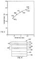
- FIG. 3 shows how the transmittance varies with reflective index of the transparent layers. Therefore, any transparent materials with a reflective index equal to or greater than 1.2 can be selected to form the multilayer cathode.
- the materials can be selected from the group consisting of fluorides, oxide, and selenide.
- the fluoride includes lithium fluoride, magnesium fluoride, calcium fluoride, strontium fluoride, or barium fluoride.
- the oxide includes silicon oxide, magnesium oxide, indium oxide, tin oxide, zinc oxide, or zirconium oxide.
- the selenide includes zinc selenide or sulfur selenide.
- the materials can be organic materials as well, as long as the materials is transparent at the wavelength of interest and their refractive indices of the materials are equal to or greater than 1.2.
- ⁇ -napthylphenylbiphenyl diamine (NPB) and Tris-(8-hydroxyquinoline) aluminum (Alq) are suitable for this application.
- a surface-emitting organic light-emitting diode 400 is illustrative which is formed in accordance with the present invention.
- the device 400 has a substrate 402, on which is disposed an anode 404.
- An organic light-emitting structure 420 is formed between the anode 404 and a cathode 410.
- the organic light-emitting structure 420 is comprised of, in sequence, an organic hole-transporting layer 422, an organic light-emitting layer 424, and an organic electron-transporting layer 426.
- the structure is distinct over the prior art of FIG.
- the cathode 410 is formed of a thin electron injecting layer 412, a semi-transparent metal layer 414, and a transparent layer 416 having a refractive index of 1.2 at least; and no sputtering is employed for film deposition.
- an electrical potential difference (not shown) is applied between the anode 404 and the cathode 410 such that the anode is at a more positive electrical potential with respect to the cathode, the cathode 410 will inject electrons into the electron-transporting layer 426, and holes will be injected from the anode 404 into the hole-transporting layer 422.
- Hole-electron recombination occurs in the light-emitting layer 424, and energy is released as light, which is emitted through the light-transmissive anode 404 and substrate 402 as well as through the cathode 410.
- a high-work function metal is serving as an anode, light is emitted only from the top cathode 410.
- the substrate 402 are electrically insulated and can either be light transmissive or opaque.
- the light transmissive property is desirable for viewing the EL emission through both the bottom and the top surface.
- the transmissive characteristic of the support is immaterial, and therefore any appropriate substrate such as opaque semiconductor and ceramic wafers can be used.
- Substrate 402 can be a transmissive substrate selected from the group of glass and plastic foil. It can be an opaque substrate, such as a single crystal semiconductor substrate selected from the group consisting of Si, Ge, GaAs, GaP, GaN, GaSb, InAs, InP, InSb, and Al x Ga l-x As, where x is from 0 to 1.
- Substrate 402 can be either undoped, lightly doped, or heavily doped.
- Substrate 402 is either bare or covered with a layer of dielectric material such as Si oxides or Si nitrides. In some applications, part of the semiconductor can be used as substrate 402 for electroluminescent devices, while the remainder of the semiconductor wafer can be processed to form drivers, switchers, or other electronic devices.
- the anode 404 is formed of a conductive and transmissive layer.
- the light transparent property of the layer 404 is desirable for viewing the EL emission through the substrate and the top electrode.
- the transmissive characteristic of the layer 404 is immaterial, and therefore any appropriate materials such as metals or metal compounds having a work function greater than 4.2 eV can be used.
- the metal includes gold, iridium, molybdenum, palladium, or platinum.
- the conductive and transmissive layer can be selected from the group consisting of metal oxides, nitrides such as gallium nitride, selenides such as zinc selenide, and sulphides such as zinc sulphide.
- the suitable metal oxides include indium-tin oxide, aluminum- or indium-doped zinc oxide, tin oxide, magnesium-indium oxide, nickel-tungsten oxide, or cadmium-tin oxide.
- the hole transporting layer of the organic EL device 422 contains at least one hole transporting aromatic tertiary amine, where the latter is understood to be a compound containing at least one trivalent nitrogen atom that is bonded only to carbon atoms, at least one of which is a member of an aromatic ring.
- the aromatic tertiary amine can be an arylamine, such as a monarylamine, diarylamine, triarylamine, or a polymeric arylamine. Exemplary monomeric triarylamines are illustrated by Klupfel and others US-A-3,180,730. Other suitable triarylamines substituted with vinyl or vinyl radicals and/or containing at least one active hydrogen containing group are disclosed by Brantley and others US-A-3,567,450 and US-A-3,658,520.
- the luminescent layer 424 of the organic EL device includes a luminescent or fluorescent material, where electroluminescence is produced as a result of electron-hole pair recombination in this region.
- the luminescent layer comprises of a single component, that is a pure material with a high fluorescent efficiency.
- a well known material is tris (8-quinolinato) aluminum, (Alq), which produces excellent green electroluminescence.
- a preferred embodiment of the luminescent layer comprises a multi-component material consisting of a host material doped with one or more components of fluorescent dyes. Using this method, highly efficient EL devices can be constructed. Simultaneously, the color of the EL devices can be tuned by using fluorescent dyes of different emission wavelengths in a common host material. This dopant scheme has been described in considerable details for EL devices using Alq as the host material by Tang and others in commonly-assigned US-A-4,769,292.
- Preferred materials for use in forming the electron transporting layer 426 of the organic EL devices of this invention are metal chelated oxinoid compounds, including chelates of oxine itself (also commonly referred to as 8-quinolinol or 8-hydroxyquinoline). Such compounds exhibit both high levels of performance and are readily fabricated in the form of thin layers.
- the multilayer transparent cathode of the invention can have applications in other electroluminescent devices.
- One of the potential applications is the use of such structures in polymer light-emitting diodes.
- An organic light-emitting structure was constructed in the following manner:
- the above structure serves as a base configuration for each of the following examples, and is given in abbreviated form as ITO/NPB(75)/Alq(75).
- An organic light-emitting device was constructed as follows: a MgAg cathode was deposited on the Alq (75) layer of the base configuration by conventional thermal vapor deposition from two sources (Mg & Ag) to a thickness of about 200 nm, so as to produce a control device having an opaque top electrode.
- An organic light-emitting device was constructed as follows: a MgAg cathode was deposited on the Alq (75) layer of the base configuration by conventional thermal vapor deposition from two sources (Mg & Ag) to a thickness of about 10 nm, and then an ITO layer was overlaid on the thin MgAg buffer layer by radio frequency sputtering so as to provide a prior art device.
- An organic light-emitting device was constructed as follows: an Ag layer was deposited on the Al (q) layer of the base configuration by conventional thermal vapor deposition to a thickness of 20 nm, and then a MgO layer was deposited on the Ag layer to a thickness of 56 nm.
- An organic light-emitting device was constructed as follows: a LiF layer was deposited on the Al (q) layer of the base configuration by conventional thermal vapor deposition to a thickness of 0.3 nm, an Al layer with a thickness of 0.6 nm was deposited on the LiF layer, and then a MgO layer was deposited on the Al layer to a thickness of 56 nm.
- An organic light-emitting device was constructed as follows: a LiF layer was deposited on the Al (q) layer of the base configuration by conventional thermal vapor deposition to a thickness of 0.3 nm, an Al layer with a thickness of 0.6 nm was deposited on the LiF layer, and then an Ag layer was deposited on the LiF layer to a thickness of 20 nm.
- An organic light-emitting device was constructed as follows: a LiF layer was deposited on the Al (q) layer of the base configuration by conventional thermal vapor deposition to a thickness of 0.3 nm, an Al layer with a thickness of 0.6 nm was deposited on the LiF layer, a silver layer with a thickness of 20 nm was deposited on the LiF layer, and then a MgO layer was deposited on the silver layer to a thickness of 56 nm.
- An organic light-emitting device was constructed as follows: a LiF layer was deposited on the Al (q) layer of the base configuration by conventional thermal vapor deposition to a thickness of 0.3 nm, an Al layer with a thickness of 0.6 nm was deposited on the LiF layer, a silver layer with a thickness of 20 nm was deposited on the LiF layer, and then an Alq layer was deposited on the silver layer to a thickness of 100 nm.
- Example B Electrical shorts were commonly observed in Example B, but the inter-electrode shorting was not observed in Examples F and G. The shorts were apparently caused by radiation damage during sputtering deposition of ITO.
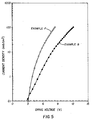
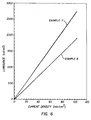
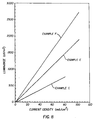
- Each of the devices was tested by applying a drive voltage between the anode and cathode, such that the anode was positive with respect to the cathode. A current-drive voltage relationship and a current-luminance relationship were then determined, and the results are shown in FIGS 5-8.
- the surface-emitting OLED of the invention exhibits better electrical and optical characteristic than that the prior art.
- the voltage required to reach a current density of 100 mA/cm is 8.5 V and 12.2 V for the devices of Examples F and B, respectively.
- the luminance of the light emitted from the top electrode with a reflective coating layer on ITO-glass is 2640 cd/m 2 and 1840 cd/m 2 for the devices of Examples F and B, respectively.
- FIGS. 7 and 8 the results obtained from Examples F, C, D and E are shown. It is clear that both electrical and optical characteristics of the surface-emitting OLED of the invention are much better than those measured on the devices with a different cathode configuration of Ag/MgO, LiF/Al/MgO, or LiF/Al/Ag.
- the device of Example C requires a much higher operating voltage than the device of Example F and exhibits a much lower electroluminescence efficiency due to the high-work-function material Ag used as an electron injector.
- Example D neither current nor luminance was detected at an operating voltage up to 20 V because the high resistive cathode blocked current transport.
- the current-voltage curve of Example E was identical to that of Example F, however, its electroluminescence efficiency was approximately 60-70% of the value measure on the device of Example F because of high reflectance of the cathode structure.
- the transparent overcoating layer can be selected from both inorganic and organic materials.
- the transparent cathode wherein the thickness of the low-work-function metal layer is in the range of 0.2 to 2.0 nm.
- the transparent cathode wherein the electron injector is formed of a 2-layer structure.
- the transparent cathode of the 2-layer structure is consisting of a thin metal fluoride layer and a thin Al outer layer.
- the transparent cathode wherein the metal fluoride can be selected from the group consisting of alkali and alkaline earth fluorides.
- the transparent cathode wherein the alkali fluoride includes lithium fluoride, sodium fluoride, potassium fluoride, rubidium fluoride, or cesium fluoride.
- the transparent cathode wherein the alkaline earth fluoride includes magnesium fluoride, calcium fluoride, strontium fluoride, or barium fluoride.
- the transparent cathode wherein the thickness of the fluoride layer is in the range of 0.2 to 2.0 nm, and the thickness of the Al layer is in the range of 0.2 to 4.0 nm.
- the transparent cathode wherein the 2-layer structure is consisting of a thin metal oxide layer and a thin Al outer layer.
- the transparent cathode wherein the metal oxide is selected from the group consisting of alkali and alkaline earth oxides.
- the transparent cathode wherein the alkali oxide includes lithium oxide, sodium oxide, potassium oxide, rubidium oxide, or cesium oxide.
- the transparent cathode wherein the alkaline earth oxide includes magnesium oxide, calcium oxide, strontium oxide, or barium oxide.
- the transparent cathode wherein the thickness of the oxide layer is in the range of 0.2 to 2.0 nm, and the thickness of the Al layer is in the range of 0.2 to 4.0 nm.
- the transparent cathode wherein the metal layer is conductive and semi-transparent.
- the transparent cathode wherein the metal layer is selected from the group consisting of silver, gold, copper, and their alloys.
- the transparent cathode wherein the thickness of the metal layer is in the range of 5-40 nm.
- the transparent cathode wherein the transparent layer is selected from the group consisting of inorganic and organic materials.
- the transparent cathode wherein the inorganic material is selected from the group consisting of fluoride, oxide, and selenide.
- the transparent cathode wherein the fluoride includes lithium fluoride, magnesium fluoride, calcium fluoride, strontium fluoride, or barium fluoride.
- the transparent cathode wherein the oxide includes silicon oxide, magnesium oxide, indium oxide, tin oxide, zinc oxide, or zirconium oxide.
- the transparent cathode wherein the selenide includes zinc selenide or sulfur selenide.
- the transparent cathode wherein the organic material includes napthylphenylbiphenyl diamine (NPB) and Tris-(8-hydroxyquinoline) aluminum (Alq).
- NPB napthylphenylbiphenyl diamine
- Alq Tris-(8-hydroxyquinoline) aluminum
- the surface-emitting organic light-emitting diode wherein the light transmissive substrate is selected from the group consisting of glass and plastic foil.
- the surface-emitting organic light-emitting diode wherein the light opaque substrate can be a single crystal semiconductor substrate selected from the group consisting of Si, Ge, GaAs, GaP, GaN, GaSb, InAs, InP, InSb, and Al x Ga l-x As, where x is from 0 to 1.
- the surface-emitting organic light-emitting diode wherein the oxide includes indium-tin oxide, aluminum- or indium-doped zinc oxide, tin oxide, magnesium-indium oxide, nickel-tungsten oxide, or cadmium-tin oxide.
- the surface-emitting organic light-emitting diode wherein the anode is a conductive and opaque layer formed from metal or metal alloys.
- the surface-emitting organic light-emitting diode wherein the metal and metal alloy include nickel, gold, iridium, molybdenum, palladium, or platinum.
- the surface-emitting organic light-emitting diode wherein the electron-transporting layer is formed of a material consisting of a metal chelated oxinoid compound.
Abstract
An transparent cathode includes an electron injector, a
metal layer over the injector, and transparent layer deposited over the metal layer
and having a refractive index equal to or greater than 1.2.
Description
- The present invention relates to transparent electron-injecting electrodes which are particularly, effective for use with surface-emitting organic light-emitting diodes.
- Conventional organic light-emitting diodes (OLED) has a transparent substrate, typically indium-tin-oxide (ITO) glass, through which the light is emitted, and the surface electrode such as MgAg is normally opaque. Surface-emitting OLED structure is of considerable interest in many display applications where high-resolution is desirable. Such a surface-emitting structure is definitely required for an active-matrix OLED display fabricated on a Si substrate, which has an important advantage of having on-chip data and scan drivers, allowing for ultra-high pixel resolution (<10 microns). Despite such importance, there was only limited success in fabricating a suitable transparent top electrode.
- G. Gu and others reported an OLED structure with a transparent top electrode consisting of a thin MgAg layer and a thicker overlying ITO film. See "Transparent organic light emitting devices" by G. Gu, V. Bulovic, P. E. Burrows, S. R. Forrest, and M. E. Thompson in Appl. Phys. Lett. 68, 2606 (1996). When ITO was deposited using a conventional sputtering process, the resulting OLED was often leaky, indicative of inter-electrode shorts. Furthermore, the forward device current was substantially lower than that of a conventional device with a thermally evaporated thick MgAg cathode. A low sputtering power of 5 W for ITO was found necessary to produce functional OLEDs without excessive shorts. However, the sputtering rate (about 0.3 nm/min) was exceedingly slow because of the low sputtering power used.
- More recently, Parthasarathy and others, and Hung and others. introduced a new transparent top electrode structure employing a thin film of copper phthalocyanine (CuPc) instead of MgAg, overlaid by a sputter-deposited ITO film. See "A metal-free cathode for organic semiconductor devices" by G. Parthasarathy, P. E. Burrows, V. Khalfin, V. G. Kozlov, and S. R. Forrest, in Appl. Phys. Lett. 72, 2138 (1998) and see " Interface engineering in preparation of organic surface-emitting diodes" by L. S. Hung and C. W. Tang in Appl. Phys. Left. 74, 3209 (1999). The CuPc apparently acts as a buffer in reducing the shorting problem caused by the ITO sputtering process. However, the CuPc layer forms an electron-injection barrier with the Alq layer, resulting in increased electron-hole recombination in the non-emissive CuPc layer, and thus a substantial reduction in EL efficiency. Incorporation of Li at the CuPc/Alq interface was necessary to reduce the injection barrier at the interface and recover the device efficiency.
- Since OLEDs are extremely sensitive to radiation, the use of a sputter-deposited ITO film to form a transparent top electrode not only increases the complexity of electrode preparation, but also introduces substantial radiation damage to OLEDs, thus resulting in device shorts and severe degradation of device performance. The use of a buffer layer is not sufficient to completely resolve the problems, and makes the process more difficult for manufactory.
- It is the object of this invention to provide a multilayer structure, which is highly transmissive and acts as an effective electron-injecting electrode in OLEDs.
- This object is achieved by a transparent cathode comprising:
- (a) an electron injector;
- (b) a metal layer over the injector; and
- (c) a transparent layer deposited over the metal layer and having a refractive index equal to or greater than 1.2.
-
- The disclosed structure in this invention can be prepared by conventional thermal evaporation in one pump-down, so that the process is significantly simplified and no radiation damage is introduced during deposition. The efficient metal-organic contact and the highly conductive metal layer ensure device operation at low voltages. As a result, the surface-emitting OLEDs have superior electrical and optical characteristics and are readily fabricated at a high short-free yield.
-
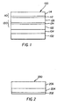
- FIG. 1 is a schematic diagram of a prior art organic surface-emitting device in which light is emitted through a thin MgAg cathode and an ITO outer layer;
- FIG. 2 is a schematic diagram of an embodiment of the multilayer transparent cathode of the invention;
- FIG. 3 shows the calculated transmittance of the multilayer cathode as a function of refractive index of the top layer;
- FIG. 4 is a schematic diagram of an embodiment of the surface-emitting organic light-emitting diodes of the invention;
- FIG. 5 shows electrical characteristics of the surface-emitting organic light-emitting diodes of the invention and the prior art;
- FIG. 6 shows optical characteristics of the surface-emitting organic light-emitting diodes of the invention and the prior art;
- FIG. 7 shows electrical characteristics of the surface-emitting organic light-emitting diodes of the invention. The properties of the devices with a different cathode structure (Ag/MgO, LiF/Al/MgO, and LiF/Al/Ag) are displayed in the figure for comparison; and
- FIG. 8 shows optical characteristics of the surface-emitting organic light-emitting diodes of the invention. The properties of the devices with a different cathode structure (Ag/MgO, LiF/Al/MgO, and LiF/Al/Ag) are displayed in the figure for comparison.
-
- The drawings are necessarily of a schematic nature, since the thicknesses of the individual layers are too thin, and thickness differences of the various elements too great to permit depiction to scale or to permit convenient proportionate scaling.
- Before describing the multilayer cathode and the surface-emitting OLEDs of the invention, one configuration of prior art surface-emitting OLED will be discussed.
- In FIG. 1, an organic light-
emitting device 100 has a light-transmissive substrate 102 on which is disposed a light-transmissive anode 104. An organic light-emitting structure 120 is formed between theanode 104 and acathode 110. The organic light-emitting structure 120 includes in sequence, an organic hole-transporting layer 122, an organic light-emitting layer 124, and an organic electron-transporting layer 126. Thecathode structure 110 is comprised, in sequence, athin MgAg layer 112 and a sputter-depositedITO layer 114. When an electrical potential difference (not shown) is applied between theanode 104 and thecathode 110 such that the anode is at a more positive electrical potential with respect to the cathode, the cathode will inject electrons into the electron-transporting layer 126, and holes will be injected from theanode 104 into the hole-transporting layer 122. Hole-electron recombination occurs in the light-emittinglayer 124, and energy is released as light, which is emitted through the light-transmissive anode 104 andsubstrate 102 as well as through thecathode 110. When an opaque substrate is used and a high-work function metal is serving as an anode, light is emitted only from thetop cathode 110. - Turning now to FIG. 2, a multilayer
transparent cathode 200 of the invention has, in order, an efficientelectron injecting layer 202, a conductive andsemi-transparent metal layer 204 over the electron injector, and atransparent layer 206 overlaid on the metal layer. The transparent layer has a reflective index equal to or greater than 1.2. - The
electron injector 202 can be formed by depositing a metal layer having a work function of less than 4 eV on the organic electron-transporting layer. The electron injector metal is selected from the group consisting of alkali, alkaline earth, and rare earth metals. The alkali metal includes lithium, sodium, potassium, rubidium, or cesium. The alkaline earth metal includes magnesium, calcium, strontium, or barium. The rare earth metal includes cerium, neodymium, samarium, europium, gadolinium, or terbium. The thickness of the low-work-function metal layer is in the range of 0.2 to 2.0 nm. - The
electron injector 202 can also be formed by depositing a 2-layer cathode on the electron-transporting layer. The 2-layer cathode is consisting of a thin inner layer of metal fluorides or oxides and a thin Al outer layer. The metal fluoride layers can be selected from alkali fluorides or alkaline earth fluorides. The metal oxide layers can be selected from alkali oxides or alkaline earth oxides. The alkali fluoride includes lithium fluoride, sodium fluoride, potassium fluoride, rubidium fluoride, or cesium fluoride; and the alkali oxide includes lithium oxide, sodium oxide, potassium oxide, rubidium oxide, or cesium oxide. The alkaline earth fluoride includes magnesium fluoride, calcium fluoride, strontium fluoride, or barium fluoride; and the alkaline earth oxide includes magnesium oxide, calcium oxide, strontium oxide, or barium oxide. The thickness of the fluoride or oxide layer is in the range of 0.2 to 2.0 nm, and the thickness of the Al layer is in the range of 0.2 to 4.0 nm. - The conductive and
semi-transparent metal layer 204 can be selected from the group consisting of silver, gold, copper, and their alloys. These materials have low electric resistivities, thus substantially reducing the sheet resistance of cathodes. The thickness of the metal layer is in the range of 5-40 nm in order to form a continuous layer and offer a high transmittance to visible light. - However, due to the high reflectance of the metal layers it is necessary to use a
transparent overcoating layer 206 which has a refractive index equal to or greater than 1.2 to reduce reflectance and thus enhance light transmission through the cathode. Computer simulation was utilized to determine light transport through two structures. The first structure is consisting of an electron injecting layer and a 20-nm thick silver layer. The second structure is consisting of an electron injecting layer, a 20-nm thick silver layer, and a 55-nm magnesium oxide layer. In both cases, the electron injecting layer was made of a 0.3-nm LiF layer and a 0.6-nm Al layer. The optical properties of the two structures were calculated as a function of light wavelength. The first structure exhibits high reflectance and low transmittance. For instance, at 550 nm (corresponding to green light) the first structure approximately shows a reflectance of 60% and a transmittance of 30%. It is of interest to note that the addition of a magnesium oxide layer on the first structure substantially reduces light reflectance, and correspondingly increases the transmittance. For instance, at 550 nm the reflectance is reduced from 60% to 30%, and correspondingly the transmittance is increased from 30% to 60%. The improvement of light transmission can also be achieved when replacing the magnesium oxide layer by other materials with a relatively large reflective index. FIG. 3 shows how the transmittance varies with reflective index of the transparent layers. Therefore, any transparent materials with a reflective index equal to or greater than 1.2 can be selected to form the multilayer cathode. The materials can be selected from the group consisting of fluorides, oxide, and selenide. The fluoride includes lithium fluoride, magnesium fluoride, calcium fluoride, strontium fluoride, or barium fluoride. The oxide includes silicon oxide, magnesium oxide, indium oxide, tin oxide, zinc oxide, or zirconium oxide. The selenide includes zinc selenide or sulfur selenide. - Besides the listed inorganic transparent dielectric materials in FIG. 3, the materials can be organic materials as well, as long as the materials is transparent at the wavelength of interest and their refractive indices of the materials are equal to or greater than 1.2. For instance, α-napthylphenylbiphenyl diamine (NPB) and Tris-(8-hydroxyquinoline) aluminum (Alq) are suitable for this application.
- In FIG. 4, a surface-emitting organic light-emitting
diode 400 is illustrative which is formed in accordance with the present invention. Here thedevice 400 has asubstrate 402, on which is disposed ananode 404. An organic light-emitting structure 420 is formed between theanode 404 and acathode 410. The organic light-emitting structure 420 is comprised of, in sequence, an organic hole-transportinglayer 422, an organic light-emittinglayer 424, and an organic electron-transportinglayer 426. The structure is distinct over the prior art of FIG. 1, as thecathode 410 is formed of a thinelectron injecting layer 412, asemi-transparent metal layer 414, and atransparent layer 416 having a refractive index of 1.2 at least; and no sputtering is employed for film deposition. When an electrical potential difference (not shown) is applied between theanode 404 and thecathode 410 such that the anode is at a more positive electrical potential with respect to the cathode, thecathode 410 will inject electrons into the electron-transportinglayer 426, and holes will be injected from theanode 404 into the hole-transportinglayer 422. Hole-electron recombination occurs in the light-emittinglayer 424, and energy is released as light, which is emitted through the light-transmissive anode 404 andsubstrate 402 as well as through thecathode 410. When an opaque substrate is used and a high-work function metal is serving as an anode, light is emitted only from thetop cathode 410. - The
substrate 402 are electrically insulated and can either be light transmissive or opaque. The light transmissive property is desirable for viewing the EL emission through both the bottom and the top surface. For applications where the EL emission is viewed through the top electrode, the transmissive characteristic of the support is immaterial, and therefore any appropriate substrate such as opaque semiconductor and ceramic wafers can be used. -
Substrate 402 can be a transmissive substrate selected from the group of glass and plastic foil. It can be an opaque substrate, such as a single crystal semiconductor substrate selected from the group consisting of Si, Ge, GaAs, GaP, GaN, GaSb, InAs, InP, InSb, and AlxGal-xAs, where x is from 0 to 1.Substrate 402 can be either undoped, lightly doped, or heavily doped.Substrate 402 is either bare or covered with a layer of dielectric material such as Si oxides or Si nitrides. In some applications, part of the semiconductor can be used assubstrate 402 for electroluminescent devices, while the remainder of the semiconductor wafer can be processed to form drivers, switchers, or other electronic devices. - The
anode 404 is formed of a conductive and transmissive layer. The light transparent property of thelayer 404 is desirable for viewing the EL emission through the substrate and the top electrode. For applications where the EL emission is viewed through the top electrode, the transmissive characteristic of thelayer 404 is immaterial, and therefore any appropriate materials such as metals or metal compounds having a work function greater than 4.2 eV can be used. The metal includes gold, iridium, molybdenum, palladium, or platinum. The conductive and transmissive layer can be selected from the group consisting of metal oxides, nitrides such as gallium nitride, selenides such as zinc selenide, and sulphides such as zinc sulphide. The suitable metal oxides include indium-tin oxide, aluminum- or indium-doped zinc oxide, tin oxide, magnesium-indium oxide, nickel-tungsten oxide, or cadmium-tin oxide. - The hole transporting layer of the
organic EL device 422 contains at least one hole transporting aromatic tertiary amine, where the latter is understood to be a compound containing at least one trivalent nitrogen atom that is bonded only to carbon atoms, at least one of which is a member of an aromatic ring. In one form the aromatic tertiary amine can be an arylamine, such as a monarylamine, diarylamine, triarylamine, or a polymeric arylamine. Exemplary monomeric triarylamines are illustrated by Klupfel and others US-A-3,180,730. Other suitable triarylamines substituted with vinyl or vinyl radicals and/or containing at least one active hydrogen containing group are disclosed by Brantley and others US-A-3,567,450 and US-A-3,658,520. - The
luminescent layer 424 of the organic EL device includes a luminescent or fluorescent material, where electroluminescence is produced as a result of electron-hole pair recombination in this region. In the simplest construction, the luminescent layer comprises of a single component, that is a pure material with a high fluorescent efficiency. A well known material is tris (8-quinolinato) aluminum, (Alq), which produces excellent green electroluminescence. A preferred embodiment of the luminescent layer comprises a multi-component material consisting of a host material doped with one or more components of fluorescent dyes. Using this method, highly efficient EL devices can be constructed. Simultaneously, the color of the EL devices can be tuned by using fluorescent dyes of different emission wavelengths in a common host material. This dopant scheme has been described in considerable details for EL devices using Alq as the host material by Tang and others in commonly-assigned US-A-4,769,292. - Preferred materials for use in forming the
electron transporting layer 426 of the organic EL devices of this invention are metal chelated oxinoid compounds, including chelates of oxine itself (also commonly referred to as 8-quinolinol or 8-hydroxyquinoline). Such compounds exhibit both high levels of performance and are readily fabricated in the form of thin layers. - The multilayer transparent cathode of the invention can have applications in other electroluminescent devices. One of the potential applications is the use of such structures in polymer light-emitting diodes.
- The following examples are presented for a further understanding of the invention. For purposes of brevity, the materials and the layers formed therefrom will be abbreviated as given below:
- ITO
- : indium tin oxide (anode)
- NPB
- : 4,4'-bis-[N-(1-naphthyl)-N-phenylamino]-bi-phenyl (hole-transporting layer)
- Alq
- : tris (8-quinolinolato-N1, 08)-aluminum (electron-transporting layer; functioning here as a combined light-emitting layer and electron-transporting layer)
- MgAg
- : magnesium: silver at a ratio of 10:1 by volume (cathode)
- MgO
- : magnesium oxide (deposited on Ag to reduce light reflection)
- Ag
- : silver (deposited on Al to reduce sheet resistance of cathodes)
- Al
- : aluminum (deposited on LiF)
- LiF
- : lithium fluoride (disposed over electron-transporting layer and combined with Al to form a electron injector))
- An organic light-emitting structure was constructed in the following manner:
- (a) a light-transmissive anode of ITO-coated glass was ultrasonicated in a commercial detergent, rinsed in deionized water, degreased in toluene vapor, and contacted by a strong oxidizing agent;
- (b) a 75 nm thick NPB hole-transporting layer was deposited on the ITO-glass by conventional thermal vapor deposition; and
- (c) a 75 nm thick Alq electron-transporting and light-emitting layer was deposited on the NPB layer by conventional thermal vapor deposition.
-
- The above structure serves as a base configuration for each of the following examples, and is given in abbreviated form as ITO/NPB(75)/Alq(75).
- An organic light-emitting device was constructed as follows: a MgAg cathode was deposited on the Alq (75) layer of the base configuration by conventional thermal vapor deposition from two sources (Mg & Ag) to a thickness of about 200 nm, so as to produce a control device having an opaque top electrode.
- An organic light-emitting device was constructed as follows: a MgAg cathode was deposited on the Alq (75) layer of the base configuration by conventional thermal vapor deposition from two sources (Mg & Ag) to a thickness of about 10 nm, and then an ITO layer was overlaid on the thin MgAg buffer layer by radio frequency sputtering so as to provide a prior art device.
- An organic light-emitting device was constructed as follows: an Ag layer was deposited on the Al (q) layer of the base configuration by conventional thermal vapor deposition to a thickness of 20 nm, and then a MgO layer was deposited on the Ag layer to a thickness of 56 nm.
- An organic light-emitting device was constructed as follows: a LiF layer was deposited on the Al (q) layer of the base configuration by conventional thermal vapor deposition to a thickness of 0.3 nm, an Al layer with a thickness of 0.6 nm was deposited on the LiF layer, and then a MgO layer was deposited on the Al layer to a thickness of 56 nm.
- An organic light-emitting device was constructed as follows: a LiF layer was deposited on the Al (q) layer of the base configuration by conventional thermal vapor deposition to a thickness of 0.3 nm, an Al layer with a thickness of 0.6 nm was deposited on the LiF layer, and then an Ag layer was deposited on the LiF layer to a thickness of 20 nm.
- An organic light-emitting device was constructed as follows: a LiF layer was deposited on the Al (q) layer of the base configuration by conventional thermal vapor deposition to a thickness of 0.3 nm, an Al layer with a thickness of 0.6 nm was deposited on the LiF layer, a silver layer with a thickness of 20 nm was deposited on the LiF layer, and then a MgO layer was deposited on the silver layer to a thickness of 56 nm.
- An organic light-emitting device was constructed as follows: a LiF layer was deposited on the Al (q) layer of the base configuration by conventional thermal vapor deposition to a thickness of 0.3 nm, an Al layer with a thickness of 0.6 nm was deposited on the LiF layer, a silver layer with a thickness of 20 nm was deposited on the LiF layer, and then an Alq layer was deposited on the silver layer to a thickness of 100 nm.
- Electrical shorts were commonly observed in Example B, but the inter-electrode shorting was not observed in Examples F and G. The shorts were apparently caused by radiation damage during sputtering deposition of ITO. Each of the devices was tested by applying a drive voltage between the anode and cathode, such that the anode was positive with respect to the cathode. A current-drive voltage relationship and a current-luminance relationship were then determined, and the results are shown in FIGS 5-8.
- Viewing FIGS. 5 and 6, it is apparent that the surface-emitting OLED of the invention exhibits better electrical and optical characteristic than that the prior art. For instance, the voltage required to reach a current density of 100 mA/cm is 8.5 V and 12.2 V for the devices of Examples F and B, respectively. Furthermore, at 100 mA/cm2 the luminance of the light emitted from the top electrode with a reflective coating layer on ITO-glass is 2640 cd/m2 and 1840 cd/m2 for the devices of Examples F and B, respectively.
- In FIGS. 7 and 8 the results obtained from Examples F, C, D and E are shown. It is clear that both electrical and optical characteristics of the surface-emitting OLED of the invention are much better than those measured on the devices with a different cathode configuration of Ag/MgO, LiF/Al/MgO, or LiF/Al/Ag. The device of Example C requires a much higher operating voltage than the device of Example F and exhibits a much lower electroluminescence efficiency due to the high-work-function material Ag used as an electron injector. For Example D, neither current nor luminance was detected at an operating voltage up to 20 V because the high resistive cathode blocked current transport. The current-voltage curve of Example E was identical to that of Example F, however, its electroluminescence efficiency was approximately 60-70% of the value measure on the device of Example F because of high reflectance of the cathode structure.
- The results obtained from the device of Example G are very similar to those from the device of Example F. Thus it indicates that the transparent overcoating layer can be selected from both inorganic and organic materials.
- Other features of the invention are included below.
- The transparent cathode wherein the thickness of the low-work-function metal layer is in the range of 0.2 to 2.0 nm.
- The transparent cathode wherein the electron injector is formed of a 2-layer structure.
- The transparent cathode of the 2-layer structure is consisting of a thin metal fluoride layer and a thin Al outer layer.
- The transparent cathode wherein the metal fluoride can be selected from the group consisting of alkali and alkaline earth fluorides.
- The transparent cathode wherein the alkali fluoride includes lithium fluoride, sodium fluoride, potassium fluoride, rubidium fluoride, or cesium fluoride.
- The transparent cathode wherein the alkaline earth fluoride includes magnesium fluoride, calcium fluoride, strontium fluoride, or barium fluoride.
- The transparent cathode wherein the thickness of the fluoride layer is in the range of 0.2 to 2.0 nm, and the thickness of the Al layer is in the range of 0.2 to 4.0 nm.
- The transparent cathode wherein the 2-layer structure is consisting of a thin metal oxide layer and a thin Al outer layer.
- The transparent cathode wherein the metal oxide is selected from the group consisting of alkali and alkaline earth oxides.
- The transparent cathode wherein the alkali oxide includes lithium oxide, sodium oxide, potassium oxide, rubidium oxide, or cesium oxide.
- The transparent cathode wherein the alkaline earth oxide includes magnesium oxide, calcium oxide, strontium oxide, or barium oxide.
- The transparent cathode wherein the thickness of the oxide layer is in the range of 0.2 to 2.0 nm, and the thickness of the Al layer is in the range of 0.2 to 4.0 nm.
- The transparent cathode wherein the metal layer is conductive and semi-transparent.
- The transparent cathode wherein the metal layer is selected from the group consisting of silver, gold, copper, and their alloys.
- The transparent cathode wherein the thickness of the metal layer is in the range of 5-40 nm.
- The transparent cathode wherein the transparent layer is selected from the group consisting of inorganic and organic materials.
- The transparent cathode wherein the inorganic material is selected from the group consisting of fluoride, oxide, and selenide.
- The transparent cathode wherein the fluoride includes lithium fluoride, magnesium fluoride, calcium fluoride, strontium fluoride, or barium fluoride.
- The transparent cathode wherein the oxide includes silicon oxide, magnesium oxide, indium oxide, tin oxide, zinc oxide, or zirconium oxide.
- The transparent cathode wherein the selenide includes zinc selenide or sulfur selenide.
- The transparent cathode wherein the organic material includes napthylphenylbiphenyl diamine (NPB) and Tris-(8-hydroxyquinoline) aluminum (Alq).
- The surface-emitting organic light-emitting diode wherein the substrate is electrically insulated and is light transmissive or opaque.
- The surface-emitting organic light-emitting diode wherein the light transmissive substrate is selected from the group consisting of glass and plastic foil.
- The surface-emitting organic light-emitting diode wherein the light opaque substrate can be a single crystal semiconductor substrate selected from the group consisting of Si, Ge, GaAs, GaP, GaN, GaSb, InAs, InP, InSb, and AlxGal-xAs, where x is from 0 to 1.
- The surface-emitting organic light-emitting diode wherein the anode is a conductive and transmissive layer formed from metal oxides.
- The surface-emitting organic light-emitting diode wherein the oxide includes indium-tin oxide, aluminum- or indium-doped zinc oxide, tin oxide, magnesium-indium oxide, nickel-tungsten oxide, or cadmium-tin oxide.
- The surface-emitting organic light-emitting diode wherein the anode is a conductive and opaque layer formed from metal or metal alloys.
- The surface-emitting organic light-emitting diode wherein the metal and metal alloy include nickel, gold, iridium, molybdenum, palladium, or platinum.
- The surface-emitting organic light-emitting diode wherein the organic hole-transporting layer is formed of a material including hole-transporting aromatic tertiary amine molecules.
- The surface-emitting organic light-emitting diode wherein the organic light-emitting layer is formed of a light-emitting host material consisting of a metal chelated oxinoid compound.
- The surface-emitting organic light-emitting diode wherein the organic light-emitting layer further includes at least one dye which emits light when dispersed in the light-emitting host material.
- The surface-emitting organic light-emitting diode wherein the electron-transporting layer is formed of a material consisting of a metal chelated oxinoid compound.
Claims (8)
- A transparent cathode comprising:(a) an electron injector;(b) a metal layer over the injector; and(c) a transparent layer deposited over the metal layer and having a refractive index equal to or greater than 1.2.
- The transparent cathode of claim 1 wherein the electron injector is formed of a metal having a work function of less than 4 eV.
- The transparent cathode of claim 2 wherein the electron injector metal is selected from the group consisting of alkali, alkaline earth, and rare earth metals.
- The transparent cathode of claim 3 wherein the alkali metal includes lithium, sodium, potassium, rubidium, or cesium.
- The transparent cathode of claim 3 wherein the alkaline earth metal includes magnesium, calcium, strontium, or barium.
- The transparent cathode of claim 3 wherein the rare earth metal includes cerium, neodymium, samarium, europium, gadolinium, or terbium.
- A surface-emitting organic light-emitting diode comprising:(a) a substrate formed of an electrically insulating material;(b) a conductive anode mounted over the substrate;(c) an organic light-emitting structure formed over the anode layer; and(d) a transparent cathode formed over the organic light-emitting structure and including:(i) an electron injector,(ii) a metal layer over the electron injector; and(iii) a transparent layer overlaid on the metal layer and having a reflective index equal to or greater than 1.2.
- The surface-emitting organic light-emitting diode of claim 7 wherein the organic light-emitting structure includes:(a) an organic hole-transporting layer formed over the anode layer;(b) an organic light-emitting layer formed over the hole-transporting layer; and(c) an organic electron-transporting layer formed over the light-emitting layer.
Applications Claiming Priority (2)
| Application Number | Priority Date | Filing Date | Title |
|---|---|---|---|
| US37181499A | 1999-08-11 | 1999-08-11 | |
| US371814 | 1999-08-11 |
Publications (1)
| Publication Number | Publication Date |
|---|---|
| EP1076368A2 true EP1076368A2 (en) | 2001-02-14 |
Family
ID=23465507
Family Applications (1)
| Application Number | Title | Priority Date | Filing Date |
|---|---|---|---|
| EP00202716A Withdrawn EP1076368A2 (en) | 1999-08-11 | 2000-07-31 | A surface-emitting organic light-emitting diode |
Country Status (2)
| Country | Link |
|---|---|
| EP (1) | EP1076368A2 (en) |
| JP (1) | JP2001052878A (en) |
Cited By (70)
| Publication number | Priority date | Publication date | Assignee | Title |
|---|---|---|---|---|
| EP1083612A2 (en) * | 1999-09-02 | 2001-03-14 | Eastman Kodak Company | Efficient electron-injection for organic electroluminescent devices |
| EP1237208A2 (en) * | 2001-02-28 | 2002-09-04 | Eastman Kodak Company | Inorganic buffer structure for organic light-emitting diode devices |
| WO2002069412A1 (en) * | 2001-02-28 | 2002-09-06 | Microemissive Displays Limited | An encapsulated electrode |
| WO2003012891A1 (en) * | 2001-07-26 | 2003-02-13 | Cambridge Display Technology Limited | Electrode compositions |
| EP1335638A1 (en) * | 2002-01-31 | 2003-08-13 | Eastman Kodak Company | Organic electroluminescent device having an adhesion-promoting layer for use with a magnesium cathode |
| US6639357B1 (en) | 2000-02-28 | 2003-10-28 | The Trustees Of Princeton University | High efficiency transparent organic light emitting devices |
| WO2004049465A2 (en) * | 2002-11-22 | 2004-06-10 | Luxell Technologies Inc. | Transparent-cathode for top-emission organic light-emitting diodes |
| EP1443806A1 (en) * | 2001-09-28 | 2004-08-04 | Sony Corporation | Organic electric field light emitting device |
| WO2004004421A3 (en) * | 2002-06-28 | 2004-08-19 | Philips Intellectual Property | Electroluminescent device with a transparent cathode |
| WO2005038942A2 (en) * | 2003-10-03 | 2005-04-28 | Eastman Kodak Company | Metal sub-layer within a hole-transporting region |
| WO2005096406A2 (en) * | 2004-03-19 | 2005-10-13 | Eastman Kodak Company | Organic light-emitting device having improved stability |
| EP1610397A2 (en) * | 2004-06-22 | 2005-12-28 | General Electric Company | Metal compound-metal multilayer electrodes for organic electronic devices |
| US7045954B2 (en) * | 2003-06-17 | 2006-05-16 | City University Of Hong Kong | Organic light-emitting device with reduction of ambient-light-reflection by disposing a multilayer structure over a semi-transparent cathode |
| EP1605531A3 (en) * | 2004-06-04 | 2006-05-17 | Lg Electronics Inc. | Organic electro-luminescent display and method for manufacturing the same |
| WO2006067200A2 (en) * | 2004-12-21 | 2006-06-29 | Thomson Licensing | Organic double-sided light-emitting diode with a light extraction dielectric layer |
| EP1701395A1 (en) * | 2005-03-11 | 2006-09-13 | Novaled GmbH | Transparent light emitting element |
| US7221332B2 (en) | 2003-12-19 | 2007-05-22 | Eastman Kodak Company | 3D stereo OLED display |
| WO2007067407A2 (en) * | 2005-12-05 | 2007-06-14 | General Electric Company | A transparent electrode for organic electronic devices |
| WO2007096538A2 (en) * | 2006-02-27 | 2007-08-30 | Commissariat A L'energie Atomique | Organic light-emitting diode with a multilayer transparent electrode |
| US7291973B2 (en) | 2001-08-29 | 2007-11-06 | Hitachi, Ltd. | Organic El display having auxiliary electrodes formed adjacent light extraction layer |
| GB2442028A (en) * | 2004-12-24 | 2008-03-26 | Cambridge Display Tech Ltd | Light emissive device |
| EP1943678A1 (en) * | 2005-11-04 | 2008-07-16 | Thomson Licensing | Electro-optical element integrating an organic electroluminescent diode and an organic transistor for modulating said diode |
| US7408191B2 (en) | 2001-05-22 | 2008-08-05 | Semiconductor Energy Laboratory Co., Ltd. | Luminescent device and process of manufacturing the same |
| DE102007024152A1 (en) * | 2007-04-18 | 2008-10-23 | Osram Opto Semiconductors Gmbh | Organic optoelectronic component |
| DE102004025578B4 (en) * | 2004-05-25 | 2009-04-23 | Applied Materials Gmbh & Co. Kg | Method for producing organic, light-emitting surface elements and use of this method |
| US7541735B2 (en) | 2003-11-21 | 2009-06-02 | Samsung Mobile Display Co., Ltd. | Organic electroluminescent device having a transparent layer |
| GB2459895A (en) * | 2008-05-09 | 2009-11-11 | Limited Cambridge Display Tech | Oled |
| DE102008034256A1 (en) * | 2008-07-18 | 2010-01-21 | Technische Universität Dresden | Photoactive component with organic layers |
| EP2161272A1 (en) | 2008-09-05 | 2010-03-10 | Basf Se | Phenanthrolines |
| EP2172990A1 (en) | 2008-10-03 | 2010-04-07 | Thomson Licensing | OLED or group of adjacent OLEDs with a light-extraction enhancement layer efficient over a large range of wavelengths |
| EP2172991A1 (en) | 2008-10-03 | 2010-04-07 | Thomson Licensing, Inc. | OLED with a composite semi-transparent electrode to enhance light-extraction over a large range of wavelengths |
| WO2010064165A1 (en) * | 2008-12-01 | 2010-06-10 | Philips Intellectual Property & Standards Gmbh | Oled device with adjustable color appearance |
| US7843125B2 (en) | 2004-01-26 | 2010-11-30 | Cambridge Display Technology Limited | Organic light emitting diode |
| US7931975B2 (en) | 2008-11-07 | 2011-04-26 | Global Oled Technology Llc | Electroluminescent device containing a flouranthene compound |
| US7947974B2 (en) | 2008-03-25 | 2011-05-24 | Global Oled Technology Llc | OLED device with hole-transport and electron-transport materials |
| US7968215B2 (en) | 2008-12-09 | 2011-06-28 | Global Oled Technology Llc | OLED device with cyclobutene electron injection materials |
| EP2355198A1 (en) | 2006-05-08 | 2011-08-10 | Global OLED Technology LLC | OLED electron-injecting layer |
| US8034465B2 (en) | 2007-06-20 | 2011-10-11 | Global Oled Technology Llc | Phosphorescent oled having double exciton-blocking layers |
| US8057916B2 (en) | 2005-04-20 | 2011-11-15 | Global Oled Technology, Llc. | OLED device with improved performance |
| US8076009B2 (en) | 2007-10-26 | 2011-12-13 | Global Oled Technology, Llc. | OLED device with fluoranthene electron transport materials |
| US8088500B2 (en) | 2008-11-12 | 2012-01-03 | Global Oled Technology Llc | OLED device with fluoranthene electron injection materials |
| US8129039B2 (en) | 2007-10-26 | 2012-03-06 | Global Oled Technology, Llc | Phosphorescent OLED device with certain fluoranthene host |
| US8147989B2 (en) | 2009-02-27 | 2012-04-03 | Global Oled Technology Llc | OLED device with stabilized green light-emitting layer |
| US8206842B2 (en) | 2009-04-06 | 2012-06-26 | Global Oled Technology Llc | Organic element for electroluminescent devices |
| US8216697B2 (en) | 2009-02-13 | 2012-07-10 | Global Oled Technology Llc | OLED with fluoranthene-macrocyclic materials |
| US8247088B2 (en) | 2008-08-28 | 2012-08-21 | Global Oled Technology Llc | Emitting complex for electroluminescent devices |
| US8253126B2 (en) | 1999-12-31 | 2012-08-28 | Lg Chem. Ltd. | Organic electronic device |
| CN102655162A (en) * | 2011-03-04 | 2012-09-05 | 三星移动显示器株式会社 | Front side emitting type organic light-emitting display device and method of manufacturing the same |
| US8314418B2 (en) | 2007-02-16 | 2012-11-20 | Osram Opto Semiconductors Gmbh | Electroluminescent organic semiconductor element and a method for repair of an electroluminescent organic semiconductor element |
| US8324800B2 (en) | 2008-06-12 | 2012-12-04 | Global Oled Technology Llc | Phosphorescent OLED device with mixed hosts |
| TWI384901B (en) * | 2006-12-26 | 2013-02-01 | Ind Tech Res Inst | Organic electroluminescent element |
| US8420229B2 (en) | 2007-10-26 | 2013-04-16 | Global OLED Technologies LLC | OLED device with certain fluoranthene light-emitting dopants |
| US8431242B2 (en) | 2007-10-26 | 2013-04-30 | Global Oled Technology, Llc. | OLED device with certain fluoranthene host |
| US8628862B2 (en) | 2007-09-20 | 2014-01-14 | Basf Se | Electroluminescent device |
| US8680693B2 (en) | 2006-01-18 | 2014-03-25 | Lg Chem. Ltd. | OLED having stacked organic light-emitting units |
| EP2752866A1 (en) | 2002-08-20 | 2014-07-09 | Global OLED Technology LLC | Color organic light emitting diode display with improved lifetime |
| US8795855B2 (en) | 2007-01-30 | 2014-08-05 | Global Oled Technology Llc | OLEDs having high efficiency and excellent lifetime |
| EP2770550A1 (en) * | 2013-02-22 | 2014-08-27 | Samsung Electronics Co., Ltd. | Photoelectronic device and image sensor |
| US8900722B2 (en) | 2007-11-29 | 2014-12-02 | Global Oled Technology Llc | OLED device employing alkali metal cluster compounds |
| US8956738B2 (en) | 2005-10-26 | 2015-02-17 | Global Oled Technology Llc | Organic element for low voltage electroluminescent devices |
| US9028979B2 (en) | 2009-06-18 | 2015-05-12 | Basf Se | Phenanthroazole compounds as hole transporting materials for electro luminescent devices |
| US9040170B2 (en) | 2004-09-20 | 2015-05-26 | Global Oled Technology Llc | Electroluminescent device with quinazoline complex emitter |
| US9118020B2 (en) | 2006-04-27 | 2015-08-25 | Global Oled Technology Llc | Electroluminescent devices including organic eil layer |
| EP3101691A1 (en) | 2002-12-16 | 2016-12-07 | Global OLED Technology LLC | A color oled display with improved power efficiency |
| US9595682B2 (en) | 2012-10-30 | 2017-03-14 | Massachusetts Institute Of Technology | Organic conductive materials and devices |
| US9666826B2 (en) | 2005-11-30 | 2017-05-30 | Global Oled Technology Llc | Electroluminescent device including an anthracene derivative |
| US9722208B2 (en) | 2014-12-31 | 2017-08-01 | Konica Minolta Laboratory U.S.A., Inc. | Light-emitting devices using thin film electrode with refractive index optimized capping layer for reduction of plasmonic energy loss |
| WO2018127128A1 (en) * | 2017-01-05 | 2018-07-12 | 昆山工研院新型平板显示技术中心有限公司 | Electrode and organic electroluminescent device using same |
| US10236450B2 (en) | 2015-03-24 | 2019-03-19 | Massachusetts Institute Of Technology | Organic conductive materials and devices |
| EP2706586B1 (en) * | 2012-09-10 | 2022-04-20 | Samsung Electronics Co., Ltd. | Light transmissive electrode, organic photoelectric device, and image sensor |
Families Citing this family (12)
| Publication number | Priority date | Publication date | Assignee | Title |
|---|---|---|---|---|
| JP4090786B2 (en) * | 2001-05-22 | 2008-05-28 | 株式会社半導体エネルギー研究所 | Light emitting device |
| JP4620298B2 (en) * | 2001-07-23 | 2011-01-26 | パイオニア株式会社 | Silver or silver alloy wiring, method for forming the same, and display panel substrate |
| KR20040021222A (en) * | 2002-09-03 | 2004-03-10 | 엘지전자 주식회사 | Organic electron luminescence device |
| JP4580160B2 (en) * | 2002-10-08 | 2010-11-10 | パイオニア株式会社 | Organic electroluminescence device |
| JP2004335207A (en) | 2003-05-02 | 2004-11-25 | Fuji Electric Holdings Co Ltd | Organic el element and its manufacturing method |
| JP2005183013A (en) * | 2003-12-16 | 2005-07-07 | Casio Comput Co Ltd | Display element, display device and manufacturing method of display element |
| JP5124083B2 (en) * | 2004-06-09 | 2013-01-23 | 三星ディスプレイ株式會社 | Organic electroluminescent display device and manufacturing method thereof |
| JP5116992B2 (en) * | 2005-05-27 | 2013-01-09 | 富士フイルム株式会社 | Organic EL device |
| US7687986B2 (en) | 2005-05-27 | 2010-03-30 | Fujifilm Corporation | Organic EL device having hole-injection layer doped with metallic oxide |
| JP2010123439A (en) * | 2008-11-20 | 2010-06-03 | Fujifilm Corp | Organic electroluminescent element |
| US8766245B2 (en) * | 2012-08-14 | 2014-07-01 | Guardian Industries Corp. | Organic light emitting diode with transparent electrode and method of making same |
| JP6388291B2 (en) * | 2014-11-17 | 2018-09-12 | 株式会社Joled | Method for manufacturing organic electroluminescent element and organic electroluminescent element |
-
2000
- 2000-07-31 EP EP00202716A patent/EP1076368A2/en not_active Withdrawn
- 2000-08-11 JP JP2000244708A patent/JP2001052878A/en active Pending
Cited By (109)
| Publication number | Priority date | Publication date | Assignee | Title |
|---|---|---|---|---|
| EP1083612A3 (en) * | 1999-09-02 | 2004-01-02 | Eastman Kodak Company | Efficient electron-injection for organic electroluminescent devices |
| EP1083612A2 (en) * | 1999-09-02 | 2001-03-14 | Eastman Kodak Company | Efficient electron-injection for organic electroluminescent devices |
| US8253126B2 (en) | 1999-12-31 | 2012-08-28 | Lg Chem. Ltd. | Organic electronic device |
| US6885149B2 (en) | 2000-02-28 | 2005-04-26 | The Trustees Of Princeton University | High efficiency transparent organic light emitting devices |
| US6639357B1 (en) | 2000-02-28 | 2003-10-28 | The Trustees Of Princeton University | High efficiency transparent organic light emitting devices |
| EP1237208A2 (en) * | 2001-02-28 | 2002-09-04 | Eastman Kodak Company | Inorganic buffer structure for organic light-emitting diode devices |
| WO2002069412A1 (en) * | 2001-02-28 | 2002-09-06 | Microemissive Displays Limited | An encapsulated electrode |
| EP1237208A3 (en) * | 2001-02-28 | 2006-06-14 | Eastman Kodak Company | Inorganic buffer structure for organic light-emitting diode devices |
| US9368561B2 (en) | 2001-05-22 | 2016-06-14 | Semiconductor Enery Laboratory Co., Ltd. | Luminescent device having light-emitting element and transistor |
| US7408191B2 (en) | 2001-05-22 | 2008-08-05 | Semiconductor Energy Laboratory Co., Ltd. | Luminescent device and process of manufacturing the same |
| US9761645B2 (en) | 2001-05-22 | 2017-09-12 | Semiconductor Energy Laboratory Co., Ltd. | Luminescent device having light emitting element and transistor |
| US10103211B2 (en) | 2001-05-22 | 2018-10-16 | Semiconductor Energy Laboratory Co., Ltd. | Luminescent device having light-emitting element and transistor |
| US8022404B2 (en) | 2001-05-22 | 2011-09-20 | Semiconductor Energy Laboratory Co., Ltd. | Luminescent device and process of manufacturing the same |
| US8803152B2 (en) | 2001-05-22 | 2014-08-12 | Semiconductor Energy Laboratory Co., Ltd. | Luminescent device and process of manufacturing the same |
| US8450741B2 (en) | 2001-05-22 | 2013-05-28 | Semiconductor Energy Laboratory Co., Ltd. | Luminescent device and process of manufacturing the same |
| WO2003012891A1 (en) * | 2001-07-26 | 2003-02-13 | Cambridge Display Technology Limited | Electrode compositions |
| US7291973B2 (en) | 2001-08-29 | 2007-11-06 | Hitachi, Ltd. | Organic El display having auxiliary electrodes formed adjacent light extraction layer |
| EP1443806A4 (en) * | 2001-09-28 | 2009-06-10 | Sony Corp | Organic electric field light emitting device |
| EP1443806A1 (en) * | 2001-09-28 | 2004-08-04 | Sony Corporation | Organic electric field light emitting device |
| US6794061B2 (en) | 2002-01-31 | 2004-09-21 | Eastman Kodak Company | Organic electroluminescent device having an adhesion-promoting layer for use with a magnesium cathode |
| EP1335638A1 (en) * | 2002-01-31 | 2003-08-13 | Eastman Kodak Company | Organic electroluminescent device having an adhesion-promoting layer for use with a magnesium cathode |
| WO2004004421A3 (en) * | 2002-06-28 | 2004-08-19 | Philips Intellectual Property | Electroluminescent device with a transparent cathode |
| US7642714B2 (en) | 2002-06-28 | 2010-01-05 | Koninklijke Philips Electronics, N.V. | Electroluminescent device with a transparent cathode |
| EP2752866A1 (en) | 2002-08-20 | 2014-07-09 | Global OLED Technology LLC | Color organic light emitting diode display with improved lifetime |
| WO2004049465A2 (en) * | 2002-11-22 | 2004-06-10 | Luxell Technologies Inc. | Transparent-cathode for top-emission organic light-emitting diodes |
| WO2004049465A3 (en) * | 2002-11-22 | 2004-11-18 | Luxell Technologies Inc | Transparent-cathode for top-emission organic light-emitting diodes |
| EP3101691A1 (en) | 2002-12-16 | 2016-12-07 | Global OLED Technology LLC | A color oled display with improved power efficiency |
| EP3101647A1 (en) | 2002-12-16 | 2016-12-07 | Global OLED Technology LLC | A color oled display with improved power efficiency |
| US7045954B2 (en) * | 2003-06-17 | 2006-05-16 | City University Of Hong Kong | Organic light-emitting device with reduction of ambient-light-reflection by disposing a multilayer structure over a semi-transparent cathode |
| WO2005038942A3 (en) * | 2003-10-03 | 2005-08-25 | Eastman Kodak Co | Metal sub-layer within a hole-transporting region |
| WO2005038942A2 (en) * | 2003-10-03 | 2005-04-28 | Eastman Kodak Company | Metal sub-layer within a hole-transporting region |
| CN1620216B (en) * | 2003-11-21 | 2010-05-05 | 三星移动显示器株式会社 | Organic electroluminescence apparatus |
| US7541735B2 (en) | 2003-11-21 | 2009-06-02 | Samsung Mobile Display Co., Ltd. | Organic electroluminescent device having a transparent layer |
| US7221332B2 (en) | 2003-12-19 | 2007-05-22 | Eastman Kodak Company | 3D stereo OLED display |
| US7843125B2 (en) | 2004-01-26 | 2010-11-30 | Cambridge Display Technology Limited | Organic light emitting diode |
| WO2005096406A2 (en) * | 2004-03-19 | 2005-10-13 | Eastman Kodak Company | Organic light-emitting device having improved stability |
| US7157156B2 (en) | 2004-03-19 | 2007-01-02 | Eastman Kodak Company | Organic light emitting device having improved stability |
| WO2005096406A3 (en) * | 2004-03-19 | 2006-04-06 | Eastman Kodak Co | Organic light-emitting device having improved stability |
| DE102004025578B4 (en) * | 2004-05-25 | 2009-04-23 | Applied Materials Gmbh & Co. Kg | Method for producing organic, light-emitting surface elements and use of this method |
| CN1708199B (en) * | 2004-06-04 | 2012-06-27 | 乐金显示有限公司 | Organic electro-luminescent display and method for manufacturing the same |
| US7619359B2 (en) | 2004-06-04 | 2009-11-17 | Lg Display Co., Ltd. | Organic electroluminescent display having sealant with grains and method for manufacturing the same |
| EP1605531A3 (en) * | 2004-06-04 | 2006-05-17 | Lg Electronics Inc. | Organic electro-luminescent display and method for manufacturing the same |
| EP1610397A3 (en) * | 2004-06-22 | 2011-08-24 | General Electric Company | Metal compound-metal multilayer electrodes for organic electronic devices |
| EP1610397A2 (en) * | 2004-06-22 | 2005-12-28 | General Electric Company | Metal compound-metal multilayer electrodes for organic electronic devices |
| US9040170B2 (en) | 2004-09-20 | 2015-05-26 | Global Oled Technology Llc | Electroluminescent device with quinazoline complex emitter |
| WO2006067200A2 (en) * | 2004-12-21 | 2006-06-29 | Thomson Licensing | Organic double-sided light-emitting diode with a light extraction dielectric layer |
| WO2006067200A3 (en) * | 2004-12-21 | 2006-12-21 | Thomson Licensing | Organic double-sided light-emitting diode with a light extraction dielectric layer |
| GB2442028A (en) * | 2004-12-24 | 2008-03-26 | Cambridge Display Tech Ltd | Light emissive device |
| US7915815B2 (en) | 2005-03-11 | 2011-03-29 | Novaled Ag | Transparent light-emitting component |
| EP1701395A1 (en) * | 2005-03-11 | 2006-09-13 | Novaled GmbH | Transparent light emitting element |
| WO2006097069A1 (en) * | 2005-03-11 | 2006-09-21 | Novaled Ag | Transparent light-emitting component |
| US8057916B2 (en) | 2005-04-20 | 2011-11-15 | Global Oled Technology, Llc. | OLED device with improved performance |
| US8956738B2 (en) | 2005-10-26 | 2015-02-17 | Global Oled Technology Llc | Organic element for low voltage electroluminescent devices |
| EP1943678A1 (en) * | 2005-11-04 | 2008-07-16 | Thomson Licensing | Electro-optical element integrating an organic electroluminescent diode and an organic transistor for modulating said diode |
| US10367049B2 (en) | 2005-11-04 | 2019-07-30 | Interdigital Ce Patent Holdings | Electro-optical element integrating an organic electroluminescent diode and an organic transistor for modulating said diode |
| US9666826B2 (en) | 2005-11-30 | 2017-05-30 | Global Oled Technology Llc | Electroluminescent device including an anthracene derivative |
| WO2007067407A3 (en) * | 2005-12-05 | 2007-11-22 | Gen Electric | A transparent electrode for organic electronic devices |
| WO2007067407A2 (en) * | 2005-12-05 | 2007-06-14 | General Electric Company | A transparent electrode for organic electronic devices |
| CN101322259B (en) * | 2005-12-05 | 2010-12-22 | 通用电气公司 | Transparent electrode for organic electronic devices |
| US8680693B2 (en) | 2006-01-18 | 2014-03-25 | Lg Chem. Ltd. | OLED having stacked organic light-emitting units |
| WO2007096538A3 (en) * | 2006-02-27 | 2007-11-01 | Commissariat Energie Atomique | Organic light-emitting diode with a multilayer transparent electrode |
| US8110984B2 (en) | 2006-02-27 | 2012-02-07 | Commissariat A L'energie Atomique | Organic light-emitting diode with transparent multilayer electrode |
| WO2007096538A2 (en) * | 2006-02-27 | 2007-08-30 | Commissariat A L'energie Atomique | Organic light-emitting diode with a multilayer transparent electrode |
| US9118020B2 (en) | 2006-04-27 | 2015-08-25 | Global Oled Technology Llc | Electroluminescent devices including organic eil layer |
| EP2355198A1 (en) | 2006-05-08 | 2011-08-10 | Global OLED Technology LLC | OLED electron-injecting layer |
| TWI384901B (en) * | 2006-12-26 | 2013-02-01 | Ind Tech Res Inst | Organic electroluminescent element |
| US8795855B2 (en) | 2007-01-30 | 2014-08-05 | Global Oled Technology Llc | OLEDs having high efficiency and excellent lifetime |
| DE102007007853B4 (en) | 2007-02-16 | 2022-03-31 | Pictiva Displays International Limited | Electroluminescent organic semiconductor element |
| US8610116B2 (en) | 2007-02-16 | 2013-12-17 | Osram Opto Semiconductors Gmbh | Electroluminescent organic semiconductor element and a method for repair of an electroluminescent organic semiconductor element |
| US8314418B2 (en) | 2007-02-16 | 2012-11-20 | Osram Opto Semiconductors Gmbh | Electroluminescent organic semiconductor element and a method for repair of an electroluminescent organic semiconductor element |
| DE102007024152A1 (en) * | 2007-04-18 | 2008-10-23 | Osram Opto Semiconductors Gmbh | Organic optoelectronic component |
| US8400054B2 (en) | 2007-04-18 | 2013-03-19 | Osram Opto Semiconductors Gmbh | Organic optoelectronic component |
| US8034465B2 (en) | 2007-06-20 | 2011-10-11 | Global Oled Technology Llc | Phosphorescent oled having double exciton-blocking layers |
| US8628862B2 (en) | 2007-09-20 | 2014-01-14 | Basf Se | Electroluminescent device |
| US8129039B2 (en) | 2007-10-26 | 2012-03-06 | Global Oled Technology, Llc | Phosphorescent OLED device with certain fluoranthene host |
| EP2568515A1 (en) | 2007-10-26 | 2013-03-13 | Global OLED Technology LLC | OLED device with fluoranthene electron transport materials |
| US8420229B2 (en) | 2007-10-26 | 2013-04-16 | Global OLED Technologies LLC | OLED device with certain fluoranthene light-emitting dopants |
| US8431242B2 (en) | 2007-10-26 | 2013-04-30 | Global Oled Technology, Llc. | OLED device with certain fluoranthene host |
| US8076009B2 (en) | 2007-10-26 | 2011-12-13 | Global Oled Technology, Llc. | OLED device with fluoranthene electron transport materials |
| US8900722B2 (en) | 2007-11-29 | 2014-12-02 | Global Oled Technology Llc | OLED device employing alkali metal cluster compounds |
| US7947974B2 (en) | 2008-03-25 | 2011-05-24 | Global Oled Technology Llc | OLED device with hole-transport and electron-transport materials |
| US8981365B2 (en) | 2008-05-09 | 2015-03-17 | Cambridge Display Technology Limited | Organic light emissive device comprising a trilayer cathode including a layer comprising sodium fluoride |
| GB2459895A (en) * | 2008-05-09 | 2009-11-11 | Limited Cambridge Display Tech | Oled |
| US8648334B2 (en) | 2008-05-09 | 2014-02-11 | Cambridge Display Technology Limited | Organic light emissive device comprising a trilayer cathode |
| GB2459895B (en) * | 2008-05-09 | 2011-04-27 | Cambridge Display Technology Limited | Organic light emissive device |
| US8324800B2 (en) | 2008-06-12 | 2012-12-04 | Global Oled Technology Llc | Phosphorescent OLED device with mixed hosts |
| DE102008034256A1 (en) * | 2008-07-18 | 2010-01-21 | Technische Universität Dresden | Photoactive component with organic layers |
| US8247088B2 (en) | 2008-08-28 | 2012-08-21 | Global Oled Technology Llc | Emitting complex for electroluminescent devices |
| EP2161272A1 (en) | 2008-09-05 | 2010-03-10 | Basf Se | Phenanthrolines |
| EP2172990A1 (en) | 2008-10-03 | 2010-04-07 | Thomson Licensing | OLED or group of adjacent OLEDs with a light-extraction enhancement layer efficient over a large range of wavelengths |
| EP2172991A1 (en) | 2008-10-03 | 2010-04-07 | Thomson Licensing, Inc. | OLED with a composite semi-transparent electrode to enhance light-extraction over a large range of wavelengths |
| EP2172992A1 (en) | 2008-10-03 | 2010-04-07 | Thomson Licensing | OLED or group of adjacent OLEDs with a light-extraction enhancement layer efficient over a large range of wavelengths |
| US7931975B2 (en) | 2008-11-07 | 2011-04-26 | Global Oled Technology Llc | Electroluminescent device containing a flouranthene compound |
| US8088500B2 (en) | 2008-11-12 | 2012-01-03 | Global Oled Technology Llc | OLED device with fluoranthene electron injection materials |
| WO2010064165A1 (en) * | 2008-12-01 | 2010-06-10 | Philips Intellectual Property & Standards Gmbh | Oled device with adjustable color appearance |
| US7968215B2 (en) | 2008-12-09 | 2011-06-28 | Global Oled Technology Llc | OLED device with cyclobutene electron injection materials |
| US8216697B2 (en) | 2009-02-13 | 2012-07-10 | Global Oled Technology Llc | OLED with fluoranthene-macrocyclic materials |
| US8147989B2 (en) | 2009-02-27 | 2012-04-03 | Global Oled Technology Llc | OLED device with stabilized green light-emitting layer |
| US8206842B2 (en) | 2009-04-06 | 2012-06-26 | Global Oled Technology Llc | Organic element for electroluminescent devices |
| US9028979B2 (en) | 2009-06-18 | 2015-05-12 | Basf Se | Phenanthroazole compounds as hole transporting materials for electro luminescent devices |
| CN102655162A (en) * | 2011-03-04 | 2012-09-05 | 三星移动显示器株式会社 | Front side emitting type organic light-emitting display device and method of manufacturing the same |
| EP2706586B1 (en) * | 2012-09-10 | 2022-04-20 | Samsung Electronics Co., Ltd. | Light transmissive electrode, organic photoelectric device, and image sensor |
| US9595682B2 (en) | 2012-10-30 | 2017-03-14 | Massachusetts Institute Of Technology | Organic conductive materials and devices |
| US10707432B2 (en) | 2013-02-22 | 2020-07-07 | Samsung Electronics Co., Ltd. | Photoelectronic device and image sensor |
| EP2770550A1 (en) * | 2013-02-22 | 2014-08-27 | Samsung Electronics Co., Ltd. | Photoelectronic device and image sensor |
| US9722208B2 (en) | 2014-12-31 | 2017-08-01 | Konica Minolta Laboratory U.S.A., Inc. | Light-emitting devices using thin film electrode with refractive index optimized capping layer for reduction of plasmonic energy loss |
| US10236450B2 (en) | 2015-03-24 | 2019-03-19 | Massachusetts Institute Of Technology | Organic conductive materials and devices |
| US10957872B2 (en) | 2017-01-05 | 2021-03-23 | Kunshan New Flat Panel Display Technology Center Co. Ltd. | Electrode and organic electroluminescent device using same |
| WO2018127128A1 (en) * | 2017-01-05 | 2018-07-12 | 昆山工研院新型平板显示技术中心有限公司 | Electrode and organic electroluminescent device using same |
Also Published As
| Publication number | Publication date |
|---|---|
| JP2001052878A (en) | 2001-02-23 |
Similar Documents
| Publication | Publication Date | Title |
|---|---|---|
| EP1076368A2 (en) | A surface-emitting organic light-emitting diode | |
| US6469437B1 (en) | Highly transparent organic light emitting device employing a non-metallic cathode | |
| US5998803A (en) | Organic light emitting device containing a hole injection enhancement layer | |
| US6558820B2 (en) | High contrast light-emitting diode devices | |
| US7488542B2 (en) | OLEDs doped with phosphorescent compounds | |
| EP1670084B1 (en) | Organic light emitting display and method for fabricating the same | |
| US7049741B2 (en) | Organic light emitting diode with improved light emission through substrate | |
| US6483236B1 (en) | Low-voltage organic light-emitting device | |
| US5981306A (en) | Method for depositing indium tin oxide layers in organic light emitting devices | |
| US6420031B1 (en) | Highly transparent non-metallic cathodes | |
| US7309956B2 (en) | Top-emitting OLED device with improved-off axis viewing performance | |
| US7002293B2 (en) | Organic light emitting diode with improved light emission through the cathode | |
| EP0903964A1 (en) | Organic electroluminescent device with inorganic electron transporting layer | |
| EP0822603A2 (en) | Bilayer electron-injecting electrode for use in an electroluminescent device | |
| US20040222737A1 (en) | Highly transparent top electrode for OLED device | |
| KR20040098055A (en) | Display devices with organic-metal mixed layer | |
| US6995391B2 (en) | Electrode structure for electronic and opto-electronic devices | |
| EP0914025A1 (en) | A multistructured electrode for use with electroluminescent devices | |
| KR100581639B1 (en) | Organic Electroluminescent Device | |
| Yamada et al. | Organic light-emitting diodes using semi-transparent anode for flexible display | |
| US20050227110A1 (en) | Organic electroluminescent element |
Legal Events
| Date | Code | Title | Description |
|---|---|---|---|
| PUAI | Public reference made under article 153(3) epc to a published international application that has entered the european phase |
Free format text: ORIGINAL CODE: 0009012 |
|
| AK | Designated contracting states |
Kind code of ref document: A2 Designated state(s): AT BE CH CY DE DK ES FI FR GB GR IE IT LI LU MC NL PT SE |
|
| AX | Request for extension of the european patent |
Free format text: AL;LT;LV;MK;RO;SI |
|
| STAA | Information on the status of an ep patent application or granted ep patent |
Free format text: STATUS: THE APPLICATION IS DEEMED TO BE WITHDRAWN |
|
| 18D | Application deemed to be withdrawn |
Effective date: 20030201 |