EP1073109A2 - Single phase perovskite ferroelectric film on platinum electrode and method for forming same - Google Patents
Single phase perovskite ferroelectric film on platinum electrode and method for forming same Download PDFInfo
- Publication number
- EP1073109A2 EP1073109A2 EP00306349A EP00306349A EP1073109A2 EP 1073109 A2 EP1073109 A2 EP 1073109A2 EP 00306349 A EP00306349 A EP 00306349A EP 00306349 A EP00306349 A EP 00306349A EP 1073109 A2 EP1073109 A2 EP 1073109A2
- Authority
- EP
- European Patent Office
- Prior art keywords
- approximately
- ferroelectric
- range
- electrode layer
- bottom electrode
- Prior art date
- Legal status (The legal status is an assumption and is not a legal conclusion. Google has not performed a legal analysis and makes no representation as to the accuracy of the status listed.)
- Withdrawn
Links
Images


Classifications
-
- C—CHEMISTRY; METALLURGY
- C23—COATING METALLIC MATERIAL; COATING MATERIAL WITH METALLIC MATERIAL; CHEMICAL SURFACE TREATMENT; DIFFUSION TREATMENT OF METALLIC MATERIAL; COATING BY VACUUM EVAPORATION, BY SPUTTERING, BY ION IMPLANTATION OR BY CHEMICAL VAPOUR DEPOSITION, IN GENERAL; INHIBITING CORROSION OF METALLIC MATERIAL OR INCRUSTATION IN GENERAL
- C23C—COATING METALLIC MATERIAL; COATING MATERIAL WITH METALLIC MATERIAL; SURFACE TREATMENT OF METALLIC MATERIAL BY DIFFUSION INTO THE SURFACE, BY CHEMICAL CONVERSION OR SUBSTITUTION; COATING BY VACUUM EVAPORATION, BY SPUTTERING, BY ION IMPLANTATION OR BY CHEMICAL VAPOUR DEPOSITION, IN GENERAL
- C23C16/00—Chemical coating by decomposition of gaseous compounds, without leaving reaction products of surface material in the coating, i.e. chemical vapour deposition [CVD] processes
- C23C16/22—Chemical coating by decomposition of gaseous compounds, without leaving reaction products of surface material in the coating, i.e. chemical vapour deposition [CVD] processes characterised by the deposition of inorganic material, other than metallic material
- C23C16/30—Deposition of compounds, mixtures or solid solutions, e.g. borides, carbides, nitrides
- C23C16/40—Oxides
- C23C16/409—Oxides of the type ABO3 with A representing alkali, alkaline earth metal or lead and B representing a refractory metal, nickel, scandium or a lanthanide
-
- H—ELECTRICITY
- H01—ELECTRIC ELEMENTS
- H01L—SEMICONDUCTOR DEVICES NOT COVERED BY CLASS H10
- H01L27/00—Devices consisting of a plurality of semiconductor or other solid-state components formed in or on a common substrate
- H01L27/02—Devices consisting of a plurality of semiconductor or other solid-state components formed in or on a common substrate including semiconductor components specially adapted for rectifying, oscillating, amplifying or switching and having at least one potential-jump barrier or surface barrier; including integrated passive circuit elements with at least one potential-jump barrier or surface barrier
- H01L27/04—Devices consisting of a plurality of semiconductor or other solid-state components formed in or on a common substrate including semiconductor components specially adapted for rectifying, oscillating, amplifying or switching and having at least one potential-jump barrier or surface barrier; including integrated passive circuit elements with at least one potential-jump barrier or surface barrier the substrate being a semiconductor body
- H01L27/10—Devices consisting of a plurality of semiconductor or other solid-state components formed in or on a common substrate including semiconductor components specially adapted for rectifying, oscillating, amplifying or switching and having at least one potential-jump barrier or surface barrier; including integrated passive circuit elements with at least one potential-jump barrier or surface barrier the substrate being a semiconductor body including a plurality of individual components in a repetitive configuration
- H01L27/105—Devices consisting of a plurality of semiconductor or other solid-state components formed in or on a common substrate including semiconductor components specially adapted for rectifying, oscillating, amplifying or switching and having at least one potential-jump barrier or surface barrier; including integrated passive circuit elements with at least one potential-jump barrier or surface barrier the substrate being a semiconductor body including a plurality of individual components in a repetitive configuration including field-effect components
-
- H—ELECTRICITY
- H01—ELECTRIC ELEMENTS
- H01L—SEMICONDUCTOR DEVICES NOT COVERED BY CLASS H10
- H01L21/00—Processes or apparatus adapted for the manufacture or treatment of semiconductor or solid state devices or of parts thereof
- H01L21/02—Manufacture or treatment of semiconductor devices or of parts thereof
- H01L21/02104—Forming layers
- H01L21/02107—Forming insulating materials on a substrate
- H01L21/02109—Forming insulating materials on a substrate characterised by the type of layer, e.g. type of material, porous/non-porous, pre-cursors, mixtures or laminates
- H01L21/02112—Forming insulating materials on a substrate characterised by the type of layer, e.g. type of material, porous/non-porous, pre-cursors, mixtures or laminates characterised by the material of the layer
- H01L21/02172—Forming insulating materials on a substrate characterised by the type of layer, e.g. type of material, porous/non-porous, pre-cursors, mixtures or laminates characterised by the material of the layer the material containing at least one metal element, e.g. metal oxides, metal nitrides, metal oxynitrides or metal carbides
- H01L21/02197—Forming insulating materials on a substrate characterised by the type of layer, e.g. type of material, porous/non-porous, pre-cursors, mixtures or laminates characterised by the material of the layer the material containing at least one metal element, e.g. metal oxides, metal nitrides, metal oxynitrides or metal carbides the material having a perovskite structure, e.g. BaTiO3
-
- H—ELECTRICITY
- H01—ELECTRIC ELEMENTS
- H01L—SEMICONDUCTOR DEVICES NOT COVERED BY CLASS H10
- H01L21/00—Processes or apparatus adapted for the manufacture or treatment of semiconductor or solid state devices or of parts thereof
- H01L21/02—Manufacture or treatment of semiconductor devices or of parts thereof
- H01L21/02104—Forming layers
- H01L21/02107—Forming insulating materials on a substrate
- H01L21/02109—Forming insulating materials on a substrate characterised by the type of layer, e.g. type of material, porous/non-porous, pre-cursors, mixtures or laminates
- H01L21/02205—Forming insulating materials on a substrate characterised by the type of layer, e.g. type of material, porous/non-porous, pre-cursors, mixtures or laminates the layer being characterised by the precursor material for deposition
-
- H—ELECTRICITY
- H01—ELECTRIC ELEMENTS
- H01L—SEMICONDUCTOR DEVICES NOT COVERED BY CLASS H10
- H01L21/00—Processes or apparatus adapted for the manufacture or treatment of semiconductor or solid state devices or of parts thereof
- H01L21/02—Manufacture or treatment of semiconductor devices or of parts thereof
- H01L21/02104—Forming layers
- H01L21/02107—Forming insulating materials on a substrate
- H01L21/02225—Forming insulating materials on a substrate characterised by the process for the formation of the insulating layer
- H01L21/0226—Forming insulating materials on a substrate characterised by the process for the formation of the insulating layer formation by a deposition process
- H01L21/02263—Forming insulating materials on a substrate characterised by the process for the formation of the insulating layer formation by a deposition process deposition from the gas or vapour phase
- H01L21/02271—Forming insulating materials on a substrate characterised by the process for the formation of the insulating layer formation by a deposition process deposition from the gas or vapour phase deposition by decomposition or reaction of gaseous or vapour phase compounds, i.e. chemical vapour deposition
-
- H—ELECTRICITY
- H01—ELECTRIC ELEMENTS
- H01L—SEMICONDUCTOR DEVICES NOT COVERED BY CLASS H10
- H01L21/00—Processes or apparatus adapted for the manufacture or treatment of semiconductor or solid state devices or of parts thereof
- H01L21/02—Manufacture or treatment of semiconductor devices or of parts thereof
- H01L21/02104—Forming layers
- H01L21/02107—Forming insulating materials on a substrate
- H01L21/02296—Forming insulating materials on a substrate characterised by the treatment performed before or after the formation of the layer
- H01L21/02318—Forming insulating materials on a substrate characterised by the treatment performed before or after the formation of the layer post-treatment
- H01L21/02337—Forming insulating materials on a substrate characterised by the treatment performed before or after the formation of the layer post-treatment treatment by exposure to a gas or vapour
-
- H—ELECTRICITY
- H01—ELECTRIC ELEMENTS
- H01L—SEMICONDUCTOR DEVICES NOT COVERED BY CLASS H10
- H01L28/00—Passive two-terminal components without a potential-jump or surface barrier for integrated circuits; Details thereof; Multistep manufacturing processes therefor
- H01L28/40—Capacitors
- H01L28/55—Capacitors with a dielectric comprising a perovskite structure material
Definitions
- the present invention relates generally to the field of integrated circuit (IC) fabrication and, more particularly, to a ferroelectric film formed on a platinum (Pt) electrode which has single phase perovskite characteristics.
- ferroelectric capacitors should have small size, low coercive field, high remanent polarization, low fatigue rate, and low leakage current.
- Some of the candidate ferroelectric materials under investigation for these applications are perovskite ferroelectrics, such as PbZr 1-x Ti x O 3 (PZT) or doped PZT, BaTiO 3 , SrTiO 3 , etc. These materials have a high Curie temperature and promising ferroelectrical properties such as large remanent polarization and low coercive field.
- PZT PbZr 1-x Ti x O 3
- SrTiO 3 SrTiO 3
- these materials have a high Curie temperature and promising ferroelectrical properties such as large remanent polarization and low coercive field.
- these perovskite ferroelectrics are known to suffer from serious degradation problems including fatigue (loss of switchable polarization with increasing reversal of polarization), aging, and leakage current,
- SBT SrBi 2 Ta 2 O 9
- PGO Lead Germanate
- Ferroelectric thin films are usually oxide ceramics with high melting temperatures. Therefore, it is very difficult to reduce the deposition temperature lower than 600 °C and still maintain the desired phases, such as in PZT and SBT films. This relationship holds regardless of deposition technique. For the most studied PZT thin films, for example, good electrical properties in conjunction, with deposition temperatures below 600° C have not been reported. This problem could be due to metastable pyrochlore phases which tend to form in this temperature range. Although low temperature depositions are possible using improved precursors or plasma to enhance the dissociation of precursors, very little research in this area has been reported.
- the fatigue-free bilayered ferroelectrics namely SrBi 2 Ta 2 O 9 or SrBi 2 Nb 2 O 9
- MOCVD MOCVD
- sol-gel sol-gel
- pulse laser deposition the deposition temperatures are still greater than 700 ° C.
- CVD bilayered ferroelectric thin films need post-annealing temperatures higher than 700 °C for long times (> 1 hr) in order to obtain ferroelectricity.
- Platinum (Pt) and other noble metals are used in IC ferroelectric capacitors.
- the use of noble metals is motivated by their inherent chemical resistance. This property is especially desirable under high temperature oxygen annealing conditions, such as those seen in the fabrication of ferroelectric capacitors.
- chemical interaction between noble metals and ferroelectric materials such as perovskite metal oxides, is negligible.
- Pt electrodes are widely used in FeRAM and DRAM device applications. Pt is a good barrier electrode, and the surface quality of ferroelectric thin films on Pt electrodes is better than that on other electrodes. But epitaxial films, or even pure phase ferroelectric materials, are difficult to deposit on Pt through low temperature MOCVD processes.
- peeling and hillock formation are related to the differences in thermal expansion and stress of Pt with neighboring IC layers during high temperature annealing.
- a layer of Ti overlying the Pt film is known to reduce stress of the Pt film, suppressing hillock formation.
- Iridium (Ir) and barrier metals have been used as a diffusion barrier to prevent oxygen diffusion.
- Both Pt and Ir electrodes have a preferred orientation (111).
- the lattice mismatch between Pt (111) or Ir (111) and various ferroelectric materials such as PZT and PGO are as listed in Table 1. From the table, it can be seen that the lattice mismatch between Ir (111) and ferroelectric materials is smaller than that of Pt (111) and ferroelectric materials.
- LATTICE MISMATCH Materials PZT(110) c ⁇ axis oriented PGO Pt (111) 12.6% 8.3% Ir (111) 10.2 5.9%
- PZT When PZT is deposited on Pt (111) electrodes at low temperatures, such as 550°C, multiple phases are formed. Namely, both pyrochlore and perovskite (ferroelectric phase) phases result.
- the single perovskite phase of PZT on Pt can be obtained only at higher deposition temperatures over 500° C, or after annealing over 650° C.
- single perovskite (ferroelectric phase) phase is easy to form at both low and high deposition temperatures.
- PGO deposition on Ir (111) the single extremely high c-axis oriented PGO can be formed. But for the PGO on Pt (111) electrodes, even it is difficult to form a single PGO phase.
- epitaxial multilayer electrodes could be used to grow epitaxial or preferred orientation ferroelectric thin films, so that the better ferroelectric properties and film uniformity are obtained.
- a method for forming a ferroelectric film comprising the steps of:
- Step b) includes epitaxially growing the ferroelectric film from the Pt bottom electrode layer, whereby a perovskite ferroelectric film is formed on Pt without high temperature annealing.
- Step a) includes epitaxially growing the first bottom electrode layer from an underlying Ir layer having a third crystalline lattice structure which is substantially the same as the Pt first adjusted lattice structure.
- the Ir layer is epitaxially grown from the underlying silicon substrate.
- a preliminary step forms a barrier layer of a material selected from the group consisting of titanium (Ti) and tantalum (Ta) overlying the silicon substrate, having a thickness in the range of approximately 100 to 500 ⁇ .
- Step a) includes forming a Pt first bottom electrode layer at a temperature in the range of approximately 100 to 250 degrees C, with a growth rate in the range of approximately 0.1 to 0.5 ⁇ per second, to a thickness in the range of approximately 100 to 1000 ⁇ .
- a ferroelectric device comprising a first bottom electrode layer of epitaxially grown platinum (Pt) having a first adjusted crystalline lattice structure.
- Pt epitaxially grown platinum
- a single phase perovskite ferroelectric film overlies the first bottom electrode layer having a second lattice structure substantially the same as the first adjusted crystalline lattice structure. In this manner, the device has both good ferroelectric properties and low leakage current.
- a second bottom electrode layer of iridium (Ir) underlies the first bottom electrode layer having a third crystalline lattice structure substantially the same as the first adjusted lattice structure.
- the Pt electrode layer has the lattice structure of the Ir electrode layer.
- the ferroelectric film is a material selected from the group consisting of PZT and lead germanate (PGO).
- the ferroelectric device further comprises a top electrode overlying the ferroelectric film to form a capacitor.
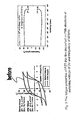
- Figs. 1, 2 and 3 show the fatigue properties of PZT thin films deposited on electrodes of Ir, Pt and Pt/Ir.
- Fig. 4 illustrates that, compared with Ir and Pt electrodes, the PZT film deposited on the Pt/Ir present invention electrode exhibits lower fatigue rates.
- Figs. 5, 6, and 7 illustrate the fatigue behavior of PZT thin films on Ir, Pt and Pt/Ir electrodes at a switching voltage of 3V and frequency of 5 kHz.
- Fig. 8 illustrates that the fatigue rates of the PZT thin films on Pt decrease with decreasing switching frequency.
- Figs. 9 and 10 illustrate the fatigue properties of PZT thin films deposited on Pt and Pt/Ir electrodes at a switching voltage of 5V and switching frequency of 5 kHz.
- Fig. 11 illustrates that, compared with the data of the PZT films at a switching voltage of 3V, the fatigue rates of the PZT thin films deposited on both Pt and Pt/Ir increase with increasing switching voltage.
- Fig. 12 illustrates the X-ray pattern of present invention PZT thin films deposited at 550°C and annealed at 650°C.
- Fig. 13 shows that the hysteresis loop of as-deposited present invention PZT thin films with a 2Pr 60.7 ⁇ C/cm 2 and a 2Ec 76 kV/cm.
- Fig. 14 illustrates the hysteresis loop of the present invention thin films after annealing at 650° C for 30 minutes.
- Fig. 15 illustrates the hysteresis loops of present invention thin films at various applied voltages.
- Fig. 16 illustrates the low leakage current of 6.16 x 10 -7 A/cm 2 at 100 kV/cm of present invention thin films.
- Fig. 17 is the X-ray pattern of Pt, Ir and epitaxial Pt/Ir electrodes.
- Fig. 18 is the X-ray patterns of PZT on Pt, Ir and epitaxial Pt-Ir electrodes.
- Fig. 19 illustrates steps in a method for forming a ferroelectric film of the present invention in a ferroelectric device.
- Fig. 20 illustrates a completed ferroelectric device of the present invention.
- the present invention describes a method of depositing epitaxial multilayer and composite electrodes, and then, depositing high quality ferroelectric thin films, such as PbZr 1-x Ti x O 3 (PZT) and Pb 5 Ge 3 O 11 (PGO) thin films, between the epitaxial multilayer and composite electrodes.
- ferroelectric thin films such as PbZr 1-x Ti x O 3 (PZT) and Pb 5 Ge 3 O 11 (PGO) thin films
- the fatigue properties of PZT thin films on three kinds of electrodes of Ir, Pt and multilayer Pt/Ir were investigated at various switching voltages and frequencies.
- the PZT thin films on Ir electrodes have square and saturated hysteresis loops, but their leakage currents and fatigue rates are very high.
- the PZT thin films on Pt electrodes have lower leakage currents, but their hysteresis loops are not square and completely saturated.
- the PZT thin films on the multilayer Pt/Ir electrodes of the present invention have very square and saturated hysteresis loops, and lower leakage currents and fatigue rates.
- the experimental prccesses and results are as follows.
- Figs. 1, 2 and 3 show the fatigue properties of PZT thin films deposited on electrodes of Ir, Pt and Pt/Ir.
- the fatigue properties were measured at a switching voltage of 3V, and a switching frequency of 50kHz.
- the normalized retained polarization of PZT thin films on Ir, Pt and Pt/Ir were 0.55, 0.61 and 0.75, respectively.
- the PZT thin films on both Ir and Pt/Ir electrodes have square and saturated hysteresis loops, but the hysteresis loop PZT thin film on Pt electrode are not square and not completely saturated.
- Fig. 4 illustrates that, compared with Ir and Pt electrodes, the PZT film deposited on the Pt/Ir present invention electrode exhibits lower fatigue rates.
- Figs. 5, 6, and 7 illustrate the fatigue behavior of PZT thin films on Ir, Pt and Pt/Ir electrodes at a switching voltage of 3V and frequency of 5 kHz.
- the normalized retained polarization of PZT thin films on Ir, Pt and Pt/Ir were 0.38, 0.76 and 0.58, respectively. Decreasing the switching frequency causes the fatigue rates of the PZT thin films deposited on Ir and Pt/Ir to increase.
- Fig. 8 illustrates that the fatigue rates of the PZT thin films on Pt decrease with decreasing switching frequency.
- Figs. 9 and 10 illustrate the fatigue properties of PZT thin films deposited on Pt and Pt/Ir electrodes at a switching voltage of 5V and switching frequency of 5 kHz. Because of the higher leakage current, the hysteresis loops of PZT thin films on Ir electrodes can be only measured up to 4V.
- Fig. 11 illustrates that, compared with the data of the PZT films at a switching voltage of 3V, the fatigue rates of the PZT thin films deposited on both Pt and Pt/Ir increase with increasing switching voltage.
- the normalized retained polarization of PZT thin films decrease significantly from 0.75 to 0.4 with increasing switching voltage from 3V to 5V.
- the normalized retained polarization of PZT thin films decrease significantly from 0.6 to 0.5 by increasing the switching voltage from 3V to 5V.
- the retained polarization of the PZT thin films deposited on Pt/Ir remains stable after 1x10 8 cycles, until almost 1x10 10 cycles (Fig. 10).
- PZT thin films An EMCORE oxide MOCVD reactor with liquid delivery system was used for the growth of PZT thin films.
- the PZT films were deposited on 6" Pt (30nm)Ir(20nm)/Ti(25nm)/SiO 2 (200nm)/Si using MOCVD processes.
- PZT THIN FILM PROPERTIES Precursors Formula Vapor Pressure (mm Hg) Decomposition Temperature(°C) Pb(TMHD) 2 Pb(C 11 H 19 O 2 ) 2 180°C/0.05 325°C Zr(TMHD) 4 Zr(C 11 H 19 O 2 ) 4 180°C/0.1 Ti(IPO) 4 Ti(C 8 H 7 O) 4 58°C/1
- [Pb(thd) 2 ], Zr(TMHD) 4 and Ti(IPO) 4 with a molar ratio of 1.2:0.5:0.5 were dissolved in a mixed solvent of butyl ether, isopropanol and tetraglyme in the molar ratio of 8:2:1. Alternately, tetrahydrofuran (THF) is used in place of butyl ether.
- the precursor solutions have a concentration of 0.1 M/L of PZT.
- the solution was injected into a vaporizer (200 - 250°C) by a pump at a rate of 0.1- 0.5 ml/min to form precursor gases.
- the precursor gases were brought into the reactor using a preheated argon flow at 200 - 250°C.
- the deposition temperatures and pressure are 500 - 650°C and 10 Torr separately.
- the shroud flow (Ar 4000 sccm) with oxygen (1000 - 2500 sccm) were led into the reactor.
- the PZT thin films were cooled down to room temperature in a oxygen atmosphere.
- as-deposited PZT thin films were annealed at 600 - 700° C with a oxygen atmosphere before and after top electrode depositions.
- compositions of the PZT thin films were analyzed by using energy dispersion X-ray analysis (EDX).
- EDX energy dispersion X-ray analysis
- the phases of the films were identified using x-ray diffraction.
- the thickness and surface morphologies of the films on Pt/Ti/SiO 2 /Si substrates were measured by Scanning Electronic Microscope.
- the ferroelectric properties were measured using a standardized RT66A tester.
- Fig. 12 illustrates the X-ray pattern of present invention PZT thin films deposited at 550°C and annealed at 650°C.
- the composition and phase measurements verify the formation of polycrystalline PZT thin films with a thickness of about 350 nm.
- Fig. 13 shows that the hysteresis loop of as-deposited present invention PZT thin film with a 2Pr (polarization voltage) 60.7 ⁇ C/cm 2 and a 2Ec (coercion field) 76 kV/cm.
- the PZT thin films have very good ferroelectric and electrical properties after deposition by MOCVD processes.
- Fig. 14 illustrates the hysteresis loop of present invention thin films after annealing at 650° C for 30 minutes.
- the 2Pr decreases to 53.8 ⁇ C/cm 2
- 2Ec increases to 87 kV/cm
- the hysteresis loop is well saturated and symmetrical at an applied voltage of 5 V.
- Fig. 15 illustrates the hysteresis loops of present invention thin films at various applied voltages.
- the hysteresis loop of the PZT thin film is almost saturated from 3 V.
- Fig. 16 illustrates the low leakage current of 6.16 x 10 -7 A/cm 2 at 100 kV/cm of present invention thin films.
- the above experimental results confirm that it is possible to deposit high quality PZT thin films using MOCVD processes.
- the epitaxial multilayer electrodes have been prepared by electrical beam evaporation techniques. First, 100 - 200 nm thick Ir electrodes were epitaxially grown on Ti/SiO 2 /Si substrates at 100 - 250°C using a lower growth rate of 0.03 - 0.06 nm/s. Then, the very thin Pt electrode from 10 - 50 nm were epitaxial grown on Ir electrode at 100 - 250°C using a lower growth rate of 0.01 - 0.05 nm/s.
- Fig. 17 is the X-ray pattern of Pt, Ir and epitaxial Pt/Ir electrodes.
- the X-ray patterns show the epitaxial Pt film grown on Ir substrate.
- compositions of the PZT thin films were analyzed by using energy dispersion X-ray analysis (EDX).
- EDX energy dispersion X-ray analysis
- the phases of the films were identified using x-ray diffraction.
- the thickness and surface morphologies of the films on the three kinds of substrates were measured by Scanning Electronic Microscope.
- the ferroelectric properties were measured using a standardized RT66A tester.
- Fig. 18 is the X-ray patterns of PZT on Pt, Ir and epitaxial Pt-Ir electrodes.
- the X-ray patterns shows the pure PZT films grown on both of Ir and epitaxial Pt/Ir electrodes.
- the MOCVD PZT thin films on epitaxial Pt/Ir also show excellent ferroelectric and electrical properties.
- Fig. 19 illustrates steps in a method for forming a ferroelectric film of the present invention in a ferroelectric device.
- Step 10 provides an integrated circuit substrate in a ferroelectric device.
- Step 12 forms a first bottom electrode layer of platinum (Pt) having a first adjusted crystalline lattice structure.
- Pt platinum
- the adjusted lattice structure is a structure specifically designed to match the lattice structure of a ferroelectric film in its perovskite phase.
- Step 12 includes forming a Pt first bottom electrode layer at a temperature in the range of approximately 100 to 250 degrees C, with a growth rate in the range of approximately 0.1 to 0.5 ⁇ per second.
- Step 12 includes the Pt first bottom electrode layer having a thickness in the range of approximately 100 to 1000 ⁇ .
- Step 14 forms a single phase perovskite ferroelectric film overlying the first bottom electrode layer having a second crystalline lattice structure substantially the same as the first adjusted crystalline lattice structure. It is understood that the first adjusted and second lattice structures are not absolutely identical. The exact mismatch is difficult to quantify. However, the lattice mismatch is small enough to cause the formation of single phase perovskite ferroelectric film on Pt, similar to manner in which such a film would be grown on an Ir electrode.
- Step 14 includes the ferroelectric film being of a material selected from the group consisting of PZT, lead germanate (PGO), and SrBi 2 Ta 2 O 9 (SBT). In some aspects of the invention, Step 14 includes forming a PZT film having a film thickness of less than approximately 1 millimeter (mm). Step 16 is a product, where an electrode having ferroelectric properties is formed on a Pt electrode.
- Step 14 includes orientationally or epitaxially growing the ferroelectric film from the Pt bottom electrode layer, whereby a perovskite ferroelectric film is formed on Pt at a low deposition temperature.
- orientationally grown implies a homogeneous polycrystalline structure with alignment in at least one axis, such as the c-axis.
- PZT film orientationally grown in the (110) orientation while PGO is formed in the (001) orientation.
- orientationally grown structures may still have crystal boundary regions between crystals.
- epiaxially grown implies an orientationally grown structure with a lack of such grain boundaries in the crystalline structure.
- Step 12 includes orientationally or epitaxially growing the first bottom electrode layer from an underlying layer having a third crystalline lattice structure, which is substantially the same as the Pt first adjusted lattice structure.
- the first adjusted and third lattice structures are not identical.
- the first adjusted lattice structure is not constant. It changes in response to the thickness of the Pt layer, with the Pt nearest the third lattice structure having a lattice structure that more closely resembles the third lattice structure.
- Step 10a forms a barrier layer of a material selected from the group consisting of titanium (Ti) and tantalum (Ta) overlying the silicon substrate, having a thickness in the range of approximately 100 to 500 ⁇ . This step is not performed in every aspect of the invention.
- Step 10b forms a second bottom electrode layer of iridium (Ir) having the third crystalline lattice structure underlying the first bottom electrode layer.
- Step 10b includes the Ir second bottom electrode layer having a thickness in the range of approximately 1000 to 2000 ⁇ .
- Step 10b includes forming the Ir second bottom electrode layer at a temperature in the range of approximately 100 to 250 degrees C, with a growth rate in the range of approximately 0.3 to 0.6 ⁇ per second. Then, Step 12 includes epitaxially growing the first bottom electrode layer from the second bottom electrode layer.
- the first adjusted lattice structure of the Pt in Step 12 is derived from the third lattice structure of the Ir deposited in Step 10b.
- the mismatch between the Ir and perovskite ferroelectric phase is very slight.
- the Pt layer "adopts" the lattice structure of the underlying Ir. That is, as long as the Pt layer is thin enough, a Pt/Ir solid solution having an Ir lattice structure is formed, following a high temperature annealing.
- Step 12 includes forming a Pt and Ir solid solution, interposed between the first and second bottom electrode layers, having the third lattice structure.
- Step 10 provides a silicon substrate and Step 10b includes orientationally or epitaxially growing the Ir second bottom electrode layer from the underlying silicon substrate.
- Step 14 includes forming a PZT ferroelectric film with the following sub-steps (not shown):
- sub-Step a) includes mixing [Pb(thd) 2 ] and [Zr(TMHD)] and Ti(IPO) 4 in a molar ratio of approximately 1.2:0.5:0.5, respectively.
- sub-Step b) includes the solvents being in a molar ratio of approximately 8:2:1, respectively. Further, sub-Step b) includes forming a precursor solution having a concentration of approximately 0.1 moles of PZT mixture per liter of solvent.
- Step 14b includes using the liquid pump to introduce the precursor solution to the precursor vaporizer in Step 14c at a rate of approximately 0.5 milliliters per minute (ml/min). Further, Step 14c includes using the precursor vaporizer to heat the precursor solution to a temperature in the range of approximately 200 to 250 degrees C, whereby the precursor gas is formed.
- Step 14c 1 mixes the precursor gas in the chamber with an argon gas shroud flow in the range of approximately 4000 to 6000 standard cubic centimeters per minute (sccm), preheated to a temperature in the range of approximately 170 to 250 degrees C.
- Step 14c 2 introduces an oxygen flow to the reactor in the range of approximately 1000 to 2500 sccm.
- Step 14c includes establishing a precursor vapor pressure in the range of approximately 30 to 100 torr (T). Further, Step 14d includes heating the wafer chuck to a temperature in the range of approximately 500 to 700 degrees C and establishing a reactor chamber pressure in the range of approximately 5 to 20 T.
- Step 15a anneals the PZT film in an oxygen atmosphere at a temperature in the range between 600 and 750 degrees C.
- Step 15b forms a conductive electrode overlying the ferroelectric film.
- Step 15c anneals, whereby a capacitor with top and bottom electrodes is formed.
- the top electrode is an Ir/Pt layered electrode, fabricated as the Pt/Ir bottom electrode.
- Steps 15a and 15c include the oxygen being introduced at a partial pressure greater that approximately 20%.
- Steps 15a and 15c include using annealing methods selected from the group consisting of furnace annealing at a temperature in the range of approximately 600 to 750 degrees C for a duration of approximately 30 minutes to 2 hours, and rapid thermal annealing (RTA) at a temperatures in the range of approximately 600 to 800 degrees C.
- annealing methods selected from the group consisting of furnace annealing at a temperature in the range of approximately 600 to 750 degrees C for a duration of approximately 30 minutes to 2 hours, and rapid thermal annealing (RTA) at a temperatures in the range of approximately 600 to 800 degrees C.
- Steps 15a and 15c include the RTA process having a duration in the range of approximately 10 to 1800 seconds, and a thermal temperature ramp-up in the range of approximately 10 to 200 degrees C per second.
- Fig. 20 illustrates a completed ferroelectric device of the present invention.
- Ferroelectric device 100 comprises a first bottom electrode layer 102 of orientationally or epitaxially grown platinum (Pt) having a first adjusted crystalline lattice structure.
- the adjusted Pt lattice structure is as described above in the explanation of Fig. 19.
- a single phase perovskite ferroelectric film 104 overlies first bottom electrode layer 102.
- Ferroelectric film 104 has a second crystalline lattice structure substantially the same as the first adjusted crystalline lattice structure, whereby the device has both good ferroelectric properties and low leakage current.
- Ferroelectric film 104 is a material selected from the group consisting of PZT, lead germanate (PGO), and SrBi 2 Ta 2 O 9 (SBT). Ferroelectric film 104 has a grain size in the range of approximately 0.5 to 5 microns.
- a second bottom electrode layer 106 of iridium (Ir) underlies first bottom electrode layer 102.
- Second bottom electrode layer 106 has a third crystalline lattice structure substantially the same as the first adjusted lattice structure, whereby the Pt electrode layer has the lattice structure of the Ir electrode layer.
- a solid solution of Pt and Ir (not shown), having an Ir lattice structure, is formed between first bottom electrode 102 and second bottom electrode 106.
- a substrate 108 underlies second bottom electrode layer 106.
- substrate 108 is a silicon substrate, whereby the ferroelectric device is fabricated on silicon for use in an integrated circuit (IC).
- IC integrated circuit
- barrier layer 110 is interposed between silicon substrate 108 and second bottom electrode layer 106.
- Barrier layer 110 includes a material selected from the group consisting of titanium (Ti) and tantalum (Ta).
- Some aspects of the invention further comprise a top electrode 112 overlying ferroelectric film 104, whereby a capacitor is formed.
- the leakage current of the capacitor formed is approximately 1 x 10 -7 A/cm 2 at 100 kV, the polarization lower voltage is approximately 3 V, and the saturation voltage is in the range of approximately 2 to 5 V.
- Ferroelectric film 104 has a thickness 114 in the range of 1000 to 8000 ⁇ .
- Ir second bottom electrode layer 106 has a thickness 116 in the range of approximately 1000 to 2000 ⁇ .
- Pt first bottom electrode layer 102 has a thickness 118 in the range of approximately 100 to 1000 ⁇ .
- a ferroelectric film which can be formed into a single phase perovskite film, on a Pt electrode, at low deposition temperatures.
- a deposition method for forming the single-phase perovskite film on the Pt bottom electrode is also provided.
- Other embodiments and variations of the above-mention ferroelectric film, ferroelectric device structure, and formation methods will occur to those skilled in the art, in response to the provision the above-cited invention.
Abstract
Description
- The present invention relates generally to the field of integrated circuit (IC) fabrication and, more particularly, to a ferroelectric film formed on a platinum (Pt) electrode which has single phase perovskite characteristics.
- In recent years, the interest in ferroelectric materials for nonvolatile random access memory application (NvRAMs) has intensified. To meet the requirements for these memory applications, ferroelectric capacitors should have small size, low coercive field, high remanent polarization, low fatigue rate, and low leakage current. Some of the candidate ferroelectric materials under investigation for these applications are perovskite ferroelectrics, such as PbZr1-xTixO3 (PZT) or doped PZT, BaTiO3, SrTiO3, etc. These materials have a high Curie temperature and promising ferroelectrical properties such as large remanent polarization and low coercive field. However, these perovskite ferroelectrics are known to suffer from serious degradation problems including fatigue (loss of switchable polarization with increasing reversal of polarization), aging, and leakage current, which affect the lifetime of the devices.
- Another ferroelectric material is SrBi2Ta2O9 (SBT), which has fatigue-free properties. However, SBT must be deposited or annealed at temperatures greater than 750°C, which limits its applications. Lead Germanate (PGO) films are another alternative material being investigated.
- Ferroelectric thin films are usually oxide ceramics with high melting temperatures. Therefore, it is very difficult to reduce the deposition temperature lower than 600 °C and still maintain the desired phases, such as in PZT and SBT films. This relationship holds regardless of deposition technique. For the most studied PZT thin films, for example, good electrical properties in conjunction, with deposition temperatures below 600° C have not been reported. This problem could be due to metastable pyrochlore phases which tend to form in this temperature range. Although low temperature depositions are possible using improved precursors or plasma to enhance the dissociation of precursors, very little research in this area has been reported. Recently, the fatigue-free bilayered ferroelectrics, namely SrBi2Ta2O9 or SrBi2Nb2O9, have been produced by MOCVD, sol-gel, and pulse laser deposition. However, the deposition temperatures are still greater than 700 ° C. Further, CVD bilayered ferroelectric thin films need post-annealing temperatures higher than 700 °C for long times (> 1 hr) in order to obtain ferroelectricity.
- Platinum (Pt) and other noble metals are used in IC ferroelectric capacitors. The use of noble metals is motivated by their inherent chemical resistance. This property is especially desirable under high temperature oxygen annealing conditions, such as those seen in the fabrication of ferroelectric capacitors. In addition, chemical interaction between noble metals and ferroelectric materials such as perovskite metal oxides, is negligible.
- Pt electrodes are widely used in FeRAM and DRAM device applications. Pt is a good barrier electrode, and the surface quality of ferroelectric thin films on Pt electrodes is better than that on other electrodes. But epitaxial films, or even pure phase ferroelectric materials, are difficult to deposit on Pt through low temperature MOCVD processes.
- Other problems associated with the annealing of a Pt metal film are peeling, hillock formation, and oxygen diffusion. Peeling and hillock formation are related to the differences in thermal expansion and stress of Pt with neighboring IC layers during high temperature annealing. A layer of Ti overlying the Pt film is known to reduce stress of the Pt film, suppressing hillock formation. Iridium (Ir) and barrier metals have been used as a diffusion barrier to prevent oxygen diffusion.
- Experimental results show that epitaxial ferroelectric thin films, such as PZT and PGO, can be grown on Ir electrodes by MOCVD processes. But due to the oxidation of Ir electrodes and diffusion of the IrO2 into ferroelectric thin films at higher deposition or annealing temperatures, these ferroelectric thin films have higher leakage current. Further, the surface roughness of ferroelectric thin films grown on Ir electrode is higher than that on electrodes such as Pt electrode, which limits the applications of Ir electrodes.
- Both Pt and Ir electrodes have a preferred orientation (111). The lattice mismatch between Pt (111) or Ir (111) and various ferroelectric materials such as PZT and PGO are as listed in Table 1. From the table, it can be seen that the lattice mismatch between Ir (111) and ferroelectric materials is smaller than that of Pt (111) and ferroelectric materials.
LATTICE MISMATCH Materials PZT(110) c·axis
oriented PGOPt (111) 12.6% 8.3% Ir (111) 10.2 5.9% - When PZT is deposited on Pt (111) electrodes at low temperatures, such as 550°C, multiple phases are formed. Namely, both pyrochlore and perovskite (ferroelectric phase) phases result. The single perovskite phase of PZT on Pt can be obtained only at higher deposition temperatures over 500° C, or after annealing over 650° C. For PZT on Ir (111) electrodes, single perovskite (ferroelectric phase) phase is easy to form at both low and high deposition temperatures. For PGO deposition on Ir (111), the single extremely high c-axis oriented PGO can be formed. But for the PGO on Pt (111) electrodes, even it is difficult to form a single PGO phase.
- The following co-pending applications, owned by the same assignee as the instant patent application, are related:
- 1) Serial No. 09/263,595, entitled "Iridium Conductive Electrode/Barrier Structure and Method for Same", invented by Zhang et al., and filed on March 5, 1999, Attorney Docket No. SMT 364;
- 2) Serial No. 09/263,970, entitled "Iridium Composite Barrier Structure and Method for Same", invented by Zhang et al., and filed on Marsh 5, 1999, Attorney Docket No. SMT 366;
- 3) Serial No. 09/316,661, entitled "Composite Iridium Barrier Structure with Oxidized Refractory Metal Companion Barrier and Method for Same", invented by Zhang et al., and filed on May 21, 1999, Attorney Docket No. SLA404;
- 4) Serial No. 09/316,646, entitled "Composite Iridium-Metal-Oxygen Barrier Structure with Refractory Metal Companion Barrier and Method for Same", invented by Zhang et al., and filed on May 21, 1999, Attorney Docket No. SLA405;
- 5) Serial No. 09/301.435, entitled "Multi-Phase Lead Germanate Film and Deposition Method", invented by Tingkai Li et al., filed on April 28, 1999, Attorney Docket No. SLA400;
- 6) Serial No. 09/301,420, entitled "C-Axis Oriented Lead Germanate Film and Deposition Method", invented by Tingkai Li et al., filed on April 28, 1999, Attorney Docket No. SLA401;
- 7) Serial No. 09/302,272, entitled "Epitaxially Grown Lead Germanate Film and Deposition Method", invented by Tingkai Li et al., filed on April 28, 1999, Attorney Docket No. SLA402;
- 8) Serial No. 09/301,434, entitled "Ferroelastic Lead Germanate Film and Deposition Method", invented by Tingkai Li et al., filed on April 28, 1999, Attorney Docket No. SLA403;
-
- It would be advantageous if a ferroelectric electrode could be fabricated that incorporated the best features of Ir and Pt.
- It would be advantageous if epitaxial multilayer electrodes could be used to grow epitaxial or preferred orientation ferroelectric thin films, so that the better ferroelectric properties and film uniformity are obtained.
- It would be advantageous if a single phase perovskite film could be formed on a metal electrode at low deposition temperatures. It would be advantageous if this perovskite film could be formed on an electrode of Pt at deposition temperatures of less than 550 degrees C.
- It would be advantageous if a ferroelectric film could be deposited on Pt, with the same perovskite properties, as a ferroelectric film deposited on Ir.
- Accordingly, in an integrated circuit ferroelectric device, a method for forming a ferroelectric film is provided comprising the steps of:
- a) forming a first bottom electrode layer of platinum (Pt) having a first adjusted crystalline lattice structure; and
- b) forming a single phase perovskite ferroelectric film overlying the first bottom electrode layer having a second crystalline lattice structure substantially the same as the first adjusted crystalline lattice structure, whereby an electrode having ferroelectric properties is formed on a Pt electrode.
-
- Step b) includes epitaxially growing the ferroelectric film from the Pt bottom electrode layer, whereby a perovskite ferroelectric film is formed on Pt without high temperature annealing.
- In some aspects of the invention, Step a) includes epitaxially growing the first bottom electrode layer from an underlying Ir layer having a third crystalline lattice structure which is substantially the same as the Pt first adjusted lattice structure. When a silicon substrate is provided, the Ir layer is epitaxially grown from the underlying silicon substrate. In some aspects of the invention, a preliminary step forms a barrier layer of a material selected from the group consisting of titanium (Ti) and tantalum (Ta) overlying the silicon substrate, having a thickness in the range of approximately 100 to 500 Å.
- Step a) includes forming a Pt first bottom electrode layer at a temperature in the range of approximately 100 to 250 degrees C, with a growth rate in the range of approximately 0.1 to 0.5 Å per second, to a thickness in the range of approximately 100 to 1000 Å.
- A ferroelectric device is also provided comprising a first bottom electrode layer of epitaxially grown platinum (Pt) having a first adjusted crystalline lattice structure. A single phase perovskite ferroelectric film overlies the first bottom electrode layer having a second lattice structure substantially the same as the first adjusted crystalline lattice structure. In this manner, the device has both good ferroelectric properties and low leakage current. A second bottom electrode layer of iridium (Ir) underlies the first bottom electrode layer having a third crystalline lattice structure substantially the same as the first adjusted lattice structure. The Pt electrode layer has the lattice structure of the Ir electrode layer.
- In some aspects of the invention, a barrier layer including a material selected from the group consisting of titanium (Ti) and tantalum (Ta), is interposed between a silicon substrate and the second bottom electrode layer. The ferroelectric film is a material selected from the group consisting of PZT and lead germanate (PGO). In some aspects of the invention, the ferroelectric device further comprises a top electrode overlying the ferroelectric film to form a capacitor.
- Figs. 1, 2 and 3 show the fatigue properties of PZT thin films deposited on electrodes of Ir, Pt and Pt/Ir.
- Fig. 4 illustrates that, compared with Ir and Pt electrodes, the PZT film deposited on the Pt/Ir present invention electrode exhibits lower fatigue rates.
- Figs. 5, 6, and 7 illustrate the fatigue behavior of PZT thin films on Ir, Pt and Pt/Ir electrodes at a switching voltage of 3V and frequency of 5 kHz.
- Fig. 8 illustrates that the fatigue rates of the PZT thin films on Pt decrease with decreasing switching frequency.
- Figs. 9 and 10 illustrate the fatigue properties of PZT thin films deposited on Pt and Pt/Ir electrodes at a switching voltage of 5V and switching frequency of 5 kHz.
- Fig. 11 illustrates that, compared with the data of the PZT films at a switching voltage of 3V, the fatigue rates of the PZT thin films deposited on both Pt and Pt/Ir increase with increasing switching voltage.
- Fig. 12 illustrates the X-ray pattern of present invention PZT thin films deposited at 550°C and annealed at 650°C.
- Fig. 13 shows that the hysteresis loop of as-deposited present invention PZT thin films with a 2Pr 60.7 µC/cm2 and a 2Ec 76 kV/cm.
- Fig. 14 illustrates the hysteresis loop of the present invention thin films after annealing at 650° C for 30 minutes.
- Fig. 15 illustrates the hysteresis loops of present invention thin films at various applied voltages.
- Fig. 16 illustrates the low leakage current of 6.16 x 10⁻⁷ A/cm2 at 100 kV/cm of present invention thin films.
- Fig. 17 is the X-ray pattern of Pt, Ir and epitaxial Pt/Ir electrodes.
- Fig. 18 is the X-ray patterns of PZT on Pt, Ir and epitaxial Pt-Ir electrodes.
- Fig. 19 illustrates steps in a method for forming a ferroelectric film of the present invention in a ferroelectric device.
- Fig. 20 illustrates a completed ferroelectric device of the present invention.
- The present invention describes a method of depositing epitaxial multilayer and composite electrodes, and then, depositing high quality ferroelectric thin films, such as PbZr1-xTixO3 (PZT) and Pb5Ge3O11 (PGO) thin films, between the epitaxial multilayer and composite electrodes.
- The fatigue properties of PZT thin films on three kinds of electrodes of Ir, Pt and multilayer Pt/Ir were investigated at various switching voltages and frequencies. The PZT thin films on Ir electrodes have square and saturated hysteresis loops, but their leakage currents and fatigue rates are very high. The PZT thin films on Pt electrodes have lower leakage currents, but their hysteresis loops are not square and completely saturated. The PZT thin films on the multilayer Pt/Ir electrodes of the present invention have very square and saturated hysteresis loops, and lower leakage currents and fatigue rates. The experimental prccesses and results are as follows.
- Figs. 1, 2 and 3 show the fatigue properties of PZT thin films deposited on electrodes of Ir, Pt and Pt/Ir. The fatigue properties were measured at a switching voltage of 3V, and a switching frequency of 50kHz. After 1x10⁸ switching cycles test, the normalized retained polarization of PZT thin films on Ir, Pt and Pt/Ir were 0.55, 0.61 and 0.75, respectively. As seen from the experimental results, the PZT thin films on both Ir and Pt/Ir electrodes have square and saturated hysteresis loops, but the hysteresis loop PZT thin film on Pt electrode are not square and not completely saturated.
- Fig. 4 illustrates that, compared with Ir and Pt electrodes, the PZT film deposited on the Pt/Ir present invention electrode exhibits lower fatigue rates.
- Figs. 5, 6, and 7 illustrate the fatigue behavior of PZT thin films on Ir, Pt and Pt/Ir electrodes at a switching voltage of 3V and frequency of 5 kHz. After 1x10⁸ switching cycles test, the normalized retained polarization of PZT thin films on Ir, Pt and Pt/Ir were 0.38, 0.76 and 0.58, respectively. Decreasing the switching frequency causes the fatigue rates of the PZT thin films deposited on Ir and Pt/Ir to increase.
- Fig. 8 illustrates that the fatigue rates of the PZT thin films on Pt decrease with decreasing switching frequency.
- Figs. 9 and 10 illustrate the fatigue properties of PZT thin films deposited on Pt and Pt/Ir electrodes at a switching voltage of 5V and switching frequency of 5 kHz. Because of the higher leakage current, the hysteresis loops of PZT thin films on Ir electrodes can be only measured up to 4V.
- Fig. 11 illustrates that, compared with the data of the PZT films at a switching voltage of 3V, the fatigue rates of the PZT thin films deposited on both Pt and Pt/Ir increase with increasing switching voltage. For the Pt electrodes, the normalized retained polarization of PZT thin films decrease significantly from 0.75 to 0.4 with increasing switching voltage from 3V to 5V. For the Pt/Ir electrodes of the present invention, the normalized retained polarization of PZT thin films decrease significantly from 0.6 to 0.5 by increasing the switching voltage from 3V to 5V. The retained polarization of the PZT thin films deposited on Pt/Ir remains stable after 1x10⁸ cycles, until almost 1x10¹⁰ cycles (Fig. 10).
- Polycrystalline PZT thin films with very good ferroelectric properties were deposited using MOCVD processes. The experimental processes and results are as stated below.
- An EMCORE oxide MOCVD reactor with liquid delivery system was used for the growth of PZT thin films. The PZT films were deposited on 6" Pt (30nm)Ir(20nm)/Ti(25nm)/SiO2(200nm)/Si using MOCVD processes. The precursors for PZT thin films listed in Table 2.
PZT THIN FILM PROPERTIES Precursors Formula Vapor Pressure (mm Hg) Decomposition Temperature(°C) Pb(TMHD)2 Pb(C11H19O2)2 180°C/0.05 325°C Zr(TMHD)4 Zr(C11H19O2)4 180°C/0.1 Ti(IPO)4 Ti(C8H7O)4 58°C/1 - [Pb(thd)2], Zr(TMHD)4 and Ti(IPO)4 with a molar ratio of 1.2:0.5:0.5 were dissolved in a mixed solvent of butyl ether, isopropanol and tetraglyme in the molar ratio of 8:2:1. Alternately, tetrahydrofuran (THF) is used in place of butyl ether. The precursor solutions have a concentration of 0.1 M/L of PZT. The solution was injected into a vaporizer (200 - 250°C) by a pump at a rate of 0.1- 0.5 ml/min to form precursor gases. The precursor gases were brought into the reactor using a preheated argon flow at 200 - 250°C. The deposition temperatures and pressure are 500 - 650°C and 10 Torr separately. The shroud flow (Ar 4000 sccm) with oxygen (1000 - 2500 sccm) were led into the reactor. After deposition, the PZT thin films were cooled down to room temperature in a oxygen atmosphere. In order to improve the ferroelectric properties of PZT thin films, as-deposited PZT thin films were annealed at 600 - 700° C with a oxygen atmosphere before and after top electrode depositions.
- The compositions of the PZT thin films were analyzed by using energy dispersion X-ray analysis (EDX). The phases of the films were identified using x-ray diffraction. The thickness and surface morphologies of the films on Pt/Ti/SiO2/Si substrates were measured by Scanning Electronic Microscope. The ferroelectric properties were measured using a standardized RT66A tester.
- Fig. 12 illustrates the X-ray pattern of present invention PZT thin films deposited at 550°C and annealed at 650°C. The composition and phase measurements verify the formation of polycrystalline PZT thin films with a thickness of about 350 nm.
- Fig. 13 shows that the hysteresis loop of as-deposited present invention PZT thin film with a 2Pr (polarization voltage) 60.7 µC/cm2 and a 2Ec (coercion field) 76 kV/cm. The PZT thin films have very good ferroelectric and electrical properties after deposition by MOCVD processes.
- Fig. 14 illustrates the hysteresis loop of present invention thin films after annealing at 650° C for 30 minutes. The 2Pr decreases to 53.8 µC/cm2, 2Ec increases to 87 kV/cm, and the hysteresis loop is well saturated and symmetrical at an applied voltage of 5 V.
- Fig. 15 illustrates the hysteresis loops of present invention thin films at various applied voltages. The hysteresis loop of the PZT thin film is almost saturated from 3 V.
- Fig. 16 illustrates the low leakage current of 6.16 x 10⁻⁷ A/cm2 at 100 kV/cm of present invention thin films. The above experimental results confirm that it is possible to deposit high quality PZT thin films using MOCVD processes.
- The epitaxial multilayer electrodes have been prepared by electrical beam evaporation techniques. First, 100 - 200 nm thick Ir electrodes were epitaxially grown on Ti/SiO2/Si substrates at 100 - 250°C using a lower growth rate of 0.03 - 0.06 nm/s. Then, the very thin Pt electrode from 10 - 50 nm were epitaxial grown on Ir electrode at 100 - 250°C using a lower growth rate of 0.01 - 0.05 nm/s.
- Fig. 17 is the X-ray pattern of Pt, Ir and epitaxial Pt/Ir electrodes. The X-ray patterns show the epitaxial Pt film grown on Ir substrate.
- The compositions of the PZT thin films were analyzed by using energy dispersion X-ray analysis (EDX). The phases of the films were identified using x-ray diffraction. The thickness and surface morphologies of the films on the three kinds of substrates were measured by Scanning Electronic Microscope. The ferroelectric properties were measured using a standardized RT66A tester.
- Fig. 18 is the X-ray patterns of PZT on Pt, Ir and epitaxial Pt-Ir electrodes. The X-ray patterns shows the pure PZT films grown on both of Ir and epitaxial Pt/Ir electrodes. The MOCVD PZT thin films on epitaxial Pt/Ir also show excellent ferroelectric and electrical properties.
- Fig. 19 illustrates steps in a method for forming a ferroelectric film of the present invention in a ferroelectric device.
Step 10 provides an integrated circuit substrate in a ferroelectric device.Step 12 forms a first bottom electrode layer of platinum (Pt) having a first adjusted crystalline lattice structure. It is understood, as stated herein, that an adjusted lattice structure is not the natural lattice structure associated with Pt. The adjusted lattice structure is a structure specifically designed to match the lattice structure of a ferroelectric film in its perovskite phase.Step 12 includes forming a Pt first bottom electrode layer at a temperature in the range of approximately 100 to 250 degrees C, with a growth rate in the range of approximately 0.1 to 0.5 Å per second.Step 12 includes the Pt first bottom electrode layer having a thickness in the range of approximately 100 to 1000 Å.Step 14 forms a single phase perovskite ferroelectric film overlying the first bottom electrode layer having a second crystalline lattice structure substantially the same as the first adjusted crystalline lattice structure. It is understood that the first adjusted and second lattice structures are not absolutely identical. The exact mismatch is difficult to quantify. However, the lattice mismatch is small enough to cause the formation of single phase perovskite ferroelectric film on Pt, similar to manner in which such a film would be grown on an Ir electrode.Step 14 includes the ferroelectric film being of a material selected from the group consisting of PZT, lead germanate (PGO), and SrBi2Ta2O9 (SBT). In some aspects of the invention,Step 14 includes forming a PZT film having a film thickness of less than approximately 1 millimeter (mm).Step 16 is a product, where an electrode having ferroelectric properties is formed on a Pt electrode. - In some aspects of the invention,
Step 14 includes orientationally or epitaxially growing the ferroelectric film from the Pt bottom electrode layer, whereby a perovskite ferroelectric film is formed on Pt at a low deposition temperature. As is well known in the art, "orientationally grown" implies a homogeneous polycrystalline structure with alignment in at least one axis, such as the c-axis. In the present invention a PZT film orientationally grown in the (110) orientation, while PGO is formed in the (001) orientation. However, orientationally grown structures may still have crystal boundary regions between crystals. "Epitaxially grown" implies an orientationally grown structure with a lack of such grain boundaries in the crystalline structure. Further,Step 12 includes orientationally or epitaxially growing the first bottom electrode layer from an underlying layer having a third crystalline lattice structure, which is substantially the same as the Pt first adjusted lattice structure. Again, the first adjusted and third lattice structures are not identical. Further, the first adjusted lattice structure is not constant. It changes in response to the thickness of the Pt layer, with the Pt nearest the third lattice structure having a lattice structure that more closely resembles the third lattice structure. - In some aspects of the invention, a further step precedes
Step 12. Step 10a (not shown) forms a barrier layer of a material selected from the group consisting of titanium (Ti) and tantalum (Ta) overlying the silicon substrate, having a thickness in the range of approximately 100 to 500 Å. This step is not performed in every aspect of the invention. Step 10b forms a second bottom electrode layer of iridium (Ir) having the third crystalline lattice structure underlying the first bottom electrode layer.Step 10b includes the Ir second bottom electrode layer having a thickness in the range of approximately 1000 to 2000 Å.Step 10b includes forming the Ir second bottom electrode layer at a temperature in the range of approximately 100 to 250 degrees C, with a growth rate in the range of approximately 0.3 to 0.6 Å per second. Then,Step 12 includes epitaxially growing the first bottom electrode layer from the second bottom electrode layer. - Thus, the first adjusted lattice structure of the Pt in
Step 12, is derived from the third lattice structure of the Ir deposited inStep 10b. The mismatch between the Ir and perovskite ferroelectric phase is very slight. As long as the Pt layer is thin enough, the Pt layer "adopts" the lattice structure of the underlying Ir. That is, as long as the Pt layer is thin enough, a Pt/Ir solid solution having an Ir lattice structure is formed, following a high temperature annealing. In some aspects of the invention it is useful to consider that a solid solution of Ir, with Pt atoms replacing some Ir atoms, or Pt atoms diffused into the Ir layer, is formed having the Ir lattice structure. If the Pt layer is thin, say 100 Å, the entire so-called Pt layer is considered to be such a solid solution. If the Pt layer is thicker, say 500 Å, then the Pt/Ir solid solution is interposed between the Ir layer and the Pt layer. Therefore,Step 12 includes forming a Pt and Ir solid solution, interposed between the first and second bottom electrode layers, having the third lattice structure. - In some aspects of the invention,
Step 10 provides a silicon substrate andStep 10b includes orientationally or epitaxially growing the Ir second bottom electrode layer from the underlying silicon substrate. - In some aspects of the invention,
Step 14 includes forming a PZT ferroelectric film with the following sub-steps (not shown): - a) mixing [Pb(thd)2] and [Zr(TMHD)] and Ti(IPO)4;
- b) dissolving the mixture with a solvent selected from the group consisting of: a) tetrahydrofuran, isopropanol, and tetraglyme; and b) butyl ether, isopropanol, and tetraglyme;
- c) heating the solution formed in sub-Step b) to create a precursor gas; and
- d) decomposing the precursor gas formed in sub-Step c) on the IC wafer to form a PZT thin film, whereby the epitaxially grown PZT film has ferroelectric properties.
-
- In some aspects of the invention, sub-Step a) includes mixing [Pb(thd)2] and [Zr(TMHD)] and Ti(IPO)4 in a molar ratio of approximately 1.2:0.5:0.5, respectively. In other aspects of the invention, sub-Step b) includes the solvents being in a molar ratio of approximately 8:2:1, respectively. Further, sub-Step b) includes forming a precursor solution having a concentration of approximately 0.1 moles of PZT mixture per liter of solvent.
- When
Step 10 provides a liquid pump and precursor vaporizer, then Step 14b includes using the liquid pump to introduce the precursor solution to the precursor vaporizer in Step 14c at a rate of approximately 0.5 milliliters per minute (ml/min). Further, Step 14c includes using the precursor vaporizer to heat the precursor solution to a temperature in the range of approximately 200 to 250 degrees C, whereby the precursor gas is formed. - When
Step 10 provides that the IC wafer is located in a reactor, then further sub-steps follow Step 14c), and precede Step 14d. Step 14c1 (not shown) mixes the precursor gas in the chamber with an argon gas shroud flow in the range of approximately 4000 to 6000 standard cubic centimeters per minute (sccm), preheated to a temperature in the range of approximately 170 to 250 degrees C. Step 14c2 (not shown) introduces an oxygen flow to the reactor in the range of approximately 1000 to 2500 sccm. - When
Step 10 provides that the IC wafer is located on a wafer chuck in a reactor, Step 14c includes establishing a precursor vapor pressure in the range of approximately 30 to 100 torr (T). Further, Step 14d includes heating the wafer chuck to a temperature in the range of approximately 500 to 700 degrees C and establishing a reactor chamber pressure in the range of approximately 5 to 20 T. - When
Step 10 provides that a ferroelectric capacitor is formed, andStep 14 includes forming a PZT ferroelectric film, then further steps followStep 14.Step 15a anneals the PZT film in an oxygen atmosphere at a temperature in the range between 600 and 750degrees C. Step 15b forms a conductive electrode overlying the ferroelectric film.Step 15c anneals, whereby a capacitor with top and bottom electrodes is formed. In some aspects of the invention, the top electrode is an Ir/Pt layered electrode, fabricated as the Pt/Ir bottom electrode. In some aspects of the invention,Steps Steps - In some aspects of the invention,
Steps - Fig. 20 illustrates a completed ferroelectric device of the present invention.
Ferroelectric device 100 comprises a firstbottom electrode layer 102 of orientationally or epitaxially grown platinum (Pt) having a first adjusted crystalline lattice structure. The adjusted Pt lattice structure is as described above in the explanation of Fig. 19. A single phase perovskiteferroelectric film 104 overlies firstbottom electrode layer 102.Ferroelectric film 104 has a second crystalline lattice structure substantially the same as the first adjusted crystalline lattice structure, whereby the device has both good ferroelectric properties and low leakage current.Ferroelectric film 104 is a material selected from the group consisting of PZT, lead germanate (PGO), and SrBi2Ta2O9 (SBT).Ferroelectric film 104 has a grain size in the range of approximately 0.5 to 5 microns. - A second
bottom electrode layer 106 of iridium (Ir) underlies firstbottom electrode layer 102. Secondbottom electrode layer 106 has a third crystalline lattice structure substantially the same as the first adjusted lattice structure, whereby the Pt electrode layer has the lattice structure of the Ir electrode layer. As explained above in the description of Fig. 19, a solid solution of Pt and Ir (not shown), having an Ir lattice structure, is formed between firstbottom electrode 102 and secondbottom electrode 106. - A
substrate 108 underlies secondbottom electrode layer 106. In some aspects of the invention,substrate 108 is a silicon substrate, whereby the ferroelectric device is fabricated on silicon for use in an integrated circuit (IC). - Optionally, a
barrier layer 110 is interposed betweensilicon substrate 108 and secondbottom electrode layer 106.Barrier layer 110 includes a material selected from the group consisting of titanium (Ti) and tantalum (Ta). - Some aspects of the invention further comprise a
top electrode 112 overlyingferroelectric film 104, whereby a capacitor is formed. The leakage current of the capacitor formed is approximately 1 x 10⁻⁷ A/cm2 at 100 kV, the polarization lower voltage is approximately 3 V, and the saturation voltage is in the range of approximately 2 to 5 V. -
Ferroelectric film 104 has athickness 114 in the range of 1000 to 8000 Å. Ir secondbottom electrode layer 106 has athickness 116 in the range of approximately 1000 to 2000 Å. Pt firstbottom electrode layer 102 has athickness 118 in the range of approximately 100 to 1000 Å. - A ferroelectric film is provided which can be formed into a single phase perovskite film, on a Pt electrode, at low deposition temperatures. The insertion of a layer of Pt between the ferroelectric film and the underlying Ir bottom electrode, dramatically improves the leakage current. Also provided is a deposition method for forming the single-phase perovskite film on the Pt bottom electrode. Other embodiments and variations of the above-mention ferroelectric film, ferroelectric device structure, and formation methods will occur to those skilled in the art, in response to the provision the above-cited invention.
Claims (34)
- In an integrated circuit ferroelectric device, a method for forming a ferroelectric film, the method comprising the steps of:a) forming a first bottom electrode layer of platinum (Pt) having a first adjusted crystalline lattice structure; andb) forming a single phase perovskite ferroelectric film overlying the first bottom electrode layer having a second crystalline lattice structure substantially the same as the first adjusted crystalline lattice structure, whereby an electrode having ferroelectric properties is formed on a Pt electrode.
- The method as in claim 1 in which Step b) includes epitaxially growing the ferroelectric film from the Pt bottom electrode layer, whereby a perovskite ferroelectric film is formed on Pt at low deposition temperatures.
- The method as in claim 1 in which Step a) includes epitaxially growing the first bottom electrode layer from an underlying layer having a third crystalline lattice structure which is substantially the same as the Pt first adjusted lattice structure.
- The method as in claim 3 including a further step preceding Step a), of:a1) forming a second bottom electrode layer of iridium (Ir) having the third crystalline lattice structure underlying the first bottom electrode layer; andin which Step a) includes epitaxially growing the first bottom electrode layer from the second bottom electrode layer.
- The method as in claim 4 wherein a silicon substrate is provided, and in which Step a1) includes epitaxially growing the Ir second bottom electrode layer from the underlying silicon substrate.
- The method as in claim 5 including a further step, preceding Step a1), of:
a2) forming a barrier layer of a material selected from the group consisting of titanium (Ti) and tantalum (Ta) overlying the silicon substrate having a thickness in the range of approximately 100 to 500 Å . - The method as in claim 4 in which Step a) includes forming a Pt and Ir solid solution, interposed between the first and second bottom electrode layers, having the third lattice structure.
- The method as in claim 4 in which Step a1) includes the Ir second bottom electrode layer having a thickness in the range of approximately 1000 to 2000 Å.
- The method as in claim 4 in which Step a1) includes forming the Ir second bottom electrode layer at a temperature in the range of approximately 100 to 250 degrees C, with a growth rate in the range of approximately 0.3 to 0.6 Å per second.
- The method as in claim 1 in which Step b) includes the ferroelectric film being of a material selected from the group consisting of PbZr1-xTixO3 (PZT), lead germanate (PGO), and SrBi2Ta2O9 (SBT).
- Tha method as in claim 1 in which Step a) includes forming a Pt first bottom electrode layer at a temperature in the range of approximately 100 to 250 degrees C, with a growth rate in the range of approximately 0.1 to 0.5 Å per second.
- The method as in claim 1 in which Step a) includes the Pt first bottom electrode layer having a thickness in the range of approximately 100 to 1000 Å.
- The method as in claim 1 in which Step b) includes forming a PZT ferroelectric film as follows:1) mixing [Pb(thd)2] and [Zr(TMHD)] and Ti(IPO)4;2) dissolving the mixture with a solvent selected from the group consisting of: a) tetrahydrofuran, isopropanol, and tetraglyme; and b) butyl ether, isopropanol, and tetraglyme;3) heating the solution formed in sub-Step 2) to create a precursor gas; and4) decomposing the precursor gas formed in sub-Step 3) on the IC wafer to form a PZT thin film, whereby the epitaxially grown PZT film has ferroelectric properties.
- The method as in claim 13 in which Step b)1) includes mixing [Pb(thd)2] and [Zr(TMHD)] and Ti(IPO)4 in a molar ratio of approximately 1.2:0.5:0.5, respectively.
- The method as in claim 13 in which Step b)2) includes the solvents being in a molar ratio of approximately 8:2:1, respectively.
- The method as in claim 13 in which Step b)2) includes forming a precursor solution having a concentration of approximately 0.1 moles of PZT mixture per liter of solvent.
- The method as in claim 13 wherein a liquid pump and precursor vaporizer are provided, in which Step b)2) includes using the liquid pump to introduce the precursor solution to the precursor vaporizer in Step b)3) at a rate of approximately 0.5 milliliters per minute (ml/min), and in which Step b)3) includes using the precursor vaporizer to heat the precursor solution to a temperature in the range of approximately 200 to 250 degrees C, whereby the precursor gas is formed.
- The method as in claim 13 in wherein the IC wafer is located in a reactor, and a further steps, following Step b)3), and preceding Step b)4), of:b)3a) mixing the precursor gas in the chamber with an argon gas shroud flow in the range of approximately 4000 to 6000 standard cubic centimeters per minute (sccm), preheated to a temperature in the range of approximately 170 to 250 degrees C; andb)3b) introducing an oxygen flow to the reactor in the range of approximately 1000 to 2500 sccm.
- The method as in claim 18 wherein the IC wafer is located on a wafer chuck in a reactor, in which Step b)3) includes establishing a precursor vapor pressure in the range of approximately 30 to 100 torr (T), and in which Step b)4) includes heating the wafer chuck to a temperature in the range of approximately 500 to 700 degrees C and establishing a reactor chamber pressure in the range of approximately 5 to 20 T.
- The method as in claim 1 wherein a ferroelectric capacitor is formed, in which Step b) includes forming a PZT ferroelectric film, and including further steps following Step c) of:d) annealing the PZT film in an oxygen atmosphere at a temperature in the range between 600 and 750 degrees C;e) forming a conductive electrode overlying the ferroelectric film; andf) annealing, whereby a capacitor with top and bottom electrodes is formed.
- The method as in claim 20 in which Steps d) and f) include the oxygen being introduced at a partial pressure greater than approximately 20%.
- The method as in claim 20 in which Steps d) and f) include using annealing methods selected from the group consisting of furnace annealing at a temperature in the range of approximately 600 to 750 degrees C for a duration of approximately 30 minutes to 2 hours, and rapid thermal annealing (RTA) at a temperatures in the range of approximately 600 to 800 degrees C.
- The method as in claim 20 in which Steps d) and f) include the RTA process having a duration in the range of approximately 10 to 1800 seconds, and a thermal temperature ramp-up in the range of approximately 10 to 200 degrees C per second.
- The method as in claim 1 in which Step b) includes forming a PZT film having a film thickness of less than approximately 1 millimeter (mm).
- A ferroelectric device comprising:a first bottom electrode layer of epitaxially grown platinum (Pt) having a first adjusted crystalline lattice structure;a single phase perovskite ferroelectric film overlying said first bottom electrode layer having a second lattice structure substantially the same as the first adjusted crystalline lattice structure, whereby the device has both good ferroelectric properties and low leakage current; anda second bottom electrode layer of iridium (Ir) underlying said first bottom electrode layer having a third crystalline lattice structure substantially the same as the first adjusted lattice structure, whereby the Pt electrode layer has the lattice structure of the Ir electrode layer.
- The ferroelectric device of claim 25 further comprising:
a silicon substrate underlying said second bottom electrode layer, whereby the ferroelectric device is fabricated on silicon for use in an integrated circuit (IC). - The ferroelectric device of claim 26 further comprising:
a barrier layer, including a material selected from the group consisting of titanium (Ti) and tantalum (Ta), interposed between said silicon substrate and said second bottom electrode layer. - The ferroelectric device of claim 25 in which said ferroelectric film is a material selected from the group consisting of PbZr1-xTixO3 (PZT), lead germanate (PGO), and SrBi2Ta2O9 (SBT).
- The ferroelectric device of claim 25 further comprising a top electrode overlying said ferroelectric film, whereby a capacitor is formed.
- The ferroelectric film of claim 29 in which the leakage current is approximately 1 x 10⁻⁷ A/cm2 at 100 kV, the polarization lower voltage is approximately 3 V, and the saturation voltage is in the range of approximately 2 to 5 V.
- The ferroelectric device of claim 25 in which said ferroelectric film has a thickness in the range of 1000 to 8000 Å.
- The ferroelectric device of claim 25 in which said Ir second bottom electrode layer has a thickness in the range of approximately 1000 to 2000 Å.
- The ferroelectric device of claim 25 in which said Pt first bottom electrode layer has a thickness in the range of approximately 100 to 1000 Å.
- The ferroelectric film of claim 25 in which said ferroelectric film has a grain size in the range of approximately 0.5 to 5 microns.
Applications Claiming Priority (2)
| Application Number | Priority Date | Filing Date | Title |
|---|---|---|---|
| US363245 | 1989-06-08 | ||
| US36324599A | 1999-07-28 | 1999-07-28 |
Publications (2)
| Publication Number | Publication Date |
|---|---|
| EP1073109A2 true EP1073109A2 (en) | 2001-01-31 |
| EP1073109A3 EP1073109A3 (en) | 2003-04-16 |
Family
ID=23429432
Family Applications (1)
| Application Number | Title | Priority Date | Filing Date |
|---|---|---|---|
| EP00306349A Withdrawn EP1073109A3 (en) | 1999-07-28 | 2000-07-26 | Single phase perovskite ferroelectric film on platinum electrode and method for forming same |
Country Status (3)
| Country | Link |
|---|---|
| EP (1) | EP1073109A3 (en) |
| JP (1) | JP2001107238A (en) |
| KR (1) | KR100451011B1 (en) |
Cited By (5)
| Publication number | Priority date | Publication date | Assignee | Title |
|---|---|---|---|---|
| EP0197635A2 (en) * | 1985-04-04 | 1986-10-15 | National Starch and Chemical Investment Holding Corporation | Acrylic emulsion copolymers for thickening aqueous systems and copolymerizable surfactant monomers for use therein |
| EP1416521A2 (en) | 2002-10-30 | 2004-05-06 | Fujitsu Limited | Manufacturing method of semiconductor device |
| CN102279308A (en) * | 2011-07-20 | 2011-12-14 | 复旦大学 | Method for measuring electric domain reverse current of insulated/leaky ferroelectric film and transforming electric domain reverse current into ferroelectric hysteresis loop |
| CN101718810B (en) * | 2009-11-26 | 2012-01-18 | 复旦大学 | Method for measuring ferroelectric hysteresis loop of leakage ferroelectric film |
| US8530321B2 (en) | 2009-12-18 | 2013-09-10 | Panasonic Corporation | Variable resistance element and manufacturing method thereof |
Families Citing this family (5)
| Publication number | Priority date | Publication date | Assignee | Title |
|---|---|---|---|---|
| KR100472724B1 (en) * | 2001-12-29 | 2005-03-08 | 주식회사 하이닉스반도체 | Method for fabrication of ferroelectric capacitor having tungsten plug |
| JP4601896B2 (en) * | 2002-10-30 | 2010-12-22 | 富士通セミコンダクター株式会社 | Semiconductor device and manufacturing method thereof |
| JP4111032B2 (en) | 2003-03-26 | 2008-07-02 | セイコーエプソン株式会社 | Ferroelectric element manufacturing method, surface acoustic wave element, inkjet head, inkjet printer, frequency filter, oscillator, electronic circuit, and electronic apparatus |
| JP5375026B2 (en) * | 2008-10-27 | 2013-12-25 | 日産自動車株式会社 | Epitaxial thin film |
| KR101845756B1 (en) * | 2016-09-29 | 2018-04-05 | 아주대학교산학협력단 | Preparing method for flexible device by controlling crystalline |
Family Cites Families (3)
| Publication number | Priority date | Publication date | Assignee | Title |
|---|---|---|---|---|
| US5874364A (en) * | 1995-03-27 | 1999-02-23 | Fujitsu Limited | Thin film deposition method, capacitor device and method for fabricating the same, and semiconductor device and method for fabricating the same |
| KR100228038B1 (en) * | 1996-02-22 | 1999-11-01 | 니시무로 타이죠 | A thin film capacitor |
| JPH10275896A (en) * | 1997-03-28 | 1998-10-13 | Murata Mfg Co Ltd | Memory element |
-
2000
- 2000-07-24 JP JP2000223129A patent/JP2001107238A/en active Pending
- 2000-07-26 EP EP00306349A patent/EP1073109A3/en not_active Withdrawn
- 2000-07-28 KR KR10-2000-0043629A patent/KR100451011B1/en not_active IP Right Cessation
Non-Patent Citations (1)
| Title |
|---|
| None * |
Cited By (7)
| Publication number | Priority date | Publication date | Assignee | Title |
|---|---|---|---|---|
| EP0197635A2 (en) * | 1985-04-04 | 1986-10-15 | National Starch and Chemical Investment Holding Corporation | Acrylic emulsion copolymers for thickening aqueous systems and copolymerizable surfactant monomers for use therein |
| EP0197635B1 (en) * | 1985-04-04 | 1991-11-13 | National Starch and Chemical Investment Holding Corporation | Acrylic emulsion copolymers for thickening aqueous systems and copolymerizable surfactant monomers for use therein |
| EP1416521A2 (en) | 2002-10-30 | 2004-05-06 | Fujitsu Limited | Manufacturing method of semiconductor device |
| EP1416521A3 (en) * | 2002-10-30 | 2007-02-28 | Fujitsu Limited | Manufacturing method of semiconductor device |
| CN101718810B (en) * | 2009-11-26 | 2012-01-18 | 复旦大学 | Method for measuring ferroelectric hysteresis loop of leakage ferroelectric film |
| US8530321B2 (en) | 2009-12-18 | 2013-09-10 | Panasonic Corporation | Variable resistance element and manufacturing method thereof |
| CN102279308A (en) * | 2011-07-20 | 2011-12-14 | 复旦大学 | Method for measuring electric domain reverse current of insulated/leaky ferroelectric film and transforming electric domain reverse current into ferroelectric hysteresis loop |
Also Published As
| Publication number | Publication date |
|---|---|
| KR20010030026A (en) | 2001-04-16 |
| EP1073109A3 (en) | 2003-04-16 |
| JP2001107238A (en) | 2001-04-17 |
| KR100451011B1 (en) | 2004-10-02 |
Similar Documents
| Publication | Publication Date | Title |
|---|---|---|
| US5572052A (en) | Electronic device using zirconate titanate and barium titanate ferroelectrics in insulating layer | |
| US7705382B2 (en) | Scalable lead zirconium titanate (PZT) thin film material and deposition method, and ferroelectric memory device structures comprising such thin film material | |
| US7309889B2 (en) | Constructions comprising perovskite-type dielectric | |
| KR100325048B1 (en) | Thin-flim capacitor and method of producing same | |
| EP0732422A2 (en) | Ferroelectric thin-film coated substrate, method for its manufacture and nonvolatile memory comprising such a substrate | |
| KR100433819B1 (en) | Process for fabricating layered superlattice materials and making electronic devices including same | |
| KR100457003B1 (en) | Multi-phase lead germanate film and deposition method | |
| US6815223B2 (en) | Low thermal budget fabrication of ferroelectric memory using RTP | |
| KR20010112236A (en) | Method for improving the sidewall stoichiometry of thin film capacitors | |
| US6190925B1 (en) | Epitaxially grown lead germanate film and deposition method | |
| US6483137B2 (en) | Capacitor utilizing c-axis oriented lead germanate film | |
| US6348705B1 (en) | Low temperature process for high density thin film integrated capacitors and amorphously frustrated ferroelectric materials therefor | |
| EP1073109A2 (en) | Single phase perovskite ferroelectric film on platinum electrode and method for forming same | |
| KR20010040303A (en) | Insulating material, substrate covered with an insulating film, method of producing the same, and thin-film device | |
| JPH1041486A (en) | Ferroelectric film for semiconductor device and forming method for the same | |
| KR100365038B1 (en) | Multi-Phase Lead Germanate Film And Deposition Method | |
| JPH09249973A (en) | Production of semiconductor device |
Legal Events
| Date | Code | Title | Description |
|---|---|---|---|
| PUAI | Public reference made under article 153(3) epc to a published international application that has entered the european phase |
Free format text: ORIGINAL CODE: 0009012 |
|
| AK | Designated contracting states |
Kind code of ref document: A2 Designated state(s): AT BE CH CY DE DK ES FI FR GB GR IE IT LI LU MC NL PT SE |
|
| AX | Request for extension of the european patent |
Free format text: AL;LT;LV;MK;RO;SI |
|
| PUAL | Search report despatched |
Free format text: ORIGINAL CODE: 0009013 |
|
| AK | Designated contracting states |
Designated state(s): AT BE CH CY DE DK ES FI FR GB GR IE IT LI LU MC NL PT SE |
|
| AX | Request for extension of the european patent |
Extension state: AL LT LV MK RO SI |
|
| 17P | Request for examination filed |
Effective date: 20030701 |
|
| AKX | Designation fees paid |
Designated state(s): DE FR GB |
|
| 17Q | First examination report despatched |
Effective date: 20061130 |
|
| STAA | Information on the status of an ep patent application or granted ep patent |
Free format text: STATUS: THE APPLICATION HAS BEEN WITHDRAWN |
|
| 18W | Application withdrawn |
Effective date: 20110510 |