EP1069458A2 - Manufacturing method for reflection type liquid crystal display - Google Patents
Manufacturing method for reflection type liquid crystal display Download PDFInfo
- Publication number
- EP1069458A2 EP1069458A2 EP00305867A EP00305867A EP1069458A2 EP 1069458 A2 EP1069458 A2 EP 1069458A2 EP 00305867 A EP00305867 A EP 00305867A EP 00305867 A EP00305867 A EP 00305867A EP 1069458 A2 EP1069458 A2 EP 1069458A2
- Authority
- EP
- European Patent Office
- Prior art keywords
- film
- photosensitive resin
- reflection
- insulating film
- mask
- Prior art date
- Legal status (The legal status is an assumption and is not a legal conclusion. Google has not performed a legal analysis and makes no representation as to the accuracy of the status listed.)
- Withdrawn
Links
Images


Classifications
-
- G—PHYSICS
- G02—OPTICS
- G02F—OPTICAL DEVICES OR ARRANGEMENTS FOR THE CONTROL OF LIGHT BY MODIFICATION OF THE OPTICAL PROPERTIES OF THE MEDIA OF THE ELEMENTS INVOLVED THEREIN; NON-LINEAR OPTICS; FREQUENCY-CHANGING OF LIGHT; OPTICAL LOGIC ELEMENTS; OPTICAL ANALOGUE/DIGITAL CONVERTERS
- G02F1/00—Devices or arrangements for the control of the intensity, colour, phase, polarisation or direction of light arriving from an independent light source, e.g. switching, gating or modulating; Non-linear optics
- G02F1/01—Devices or arrangements for the control of the intensity, colour, phase, polarisation or direction of light arriving from an independent light source, e.g. switching, gating or modulating; Non-linear optics for the control of the intensity, phase, polarisation or colour
- G02F1/13—Devices or arrangements for the control of the intensity, colour, phase, polarisation or direction of light arriving from an independent light source, e.g. switching, gating or modulating; Non-linear optics for the control of the intensity, phase, polarisation or colour based on liquid crystals, e.g. single liquid crystal display cells
- G02F1/133—Constructional arrangements; Operation of liquid crystal cells; Circuit arrangements
- G02F1/136—Liquid crystal cells structurally associated with a semi-conducting layer or substrate, e.g. cells forming part of an integrated circuit
-
- G—PHYSICS
- G02—OPTICS
- G02F—OPTICAL DEVICES OR ARRANGEMENTS FOR THE CONTROL OF LIGHT BY MODIFICATION OF THE OPTICAL PROPERTIES OF THE MEDIA OF THE ELEMENTS INVOLVED THEREIN; NON-LINEAR OPTICS; FREQUENCY-CHANGING OF LIGHT; OPTICAL LOGIC ELEMENTS; OPTICAL ANALOGUE/DIGITAL CONVERTERS
- G02F1/00—Devices or arrangements for the control of the intensity, colour, phase, polarisation or direction of light arriving from an independent light source, e.g. switching, gating or modulating; Non-linear optics
- G02F1/01—Devices or arrangements for the control of the intensity, colour, phase, polarisation or direction of light arriving from an independent light source, e.g. switching, gating or modulating; Non-linear optics for the control of the intensity, phase, polarisation or colour
- G02F1/13—Devices or arrangements for the control of the intensity, colour, phase, polarisation or direction of light arriving from an independent light source, e.g. switching, gating or modulating; Non-linear optics for the control of the intensity, phase, polarisation or colour based on liquid crystals, e.g. single liquid crystal display cells
- G02F1/133—Constructional arrangements; Operation of liquid crystal cells; Circuit arrangements
- G02F1/1333—Constructional arrangements; Manufacturing methods
- G02F1/1335—Structural association of cells with optical devices, e.g. polarisers or reflectors
- G02F1/133553—Reflecting elements
-
- G—PHYSICS
- G02—OPTICS
- G02F—OPTICAL DEVICES OR ARRANGEMENTS FOR THE CONTROL OF LIGHT BY MODIFICATION OF THE OPTICAL PROPERTIES OF THE MEDIA OF THE ELEMENTS INVOLVED THEREIN; NON-LINEAR OPTICS; FREQUENCY-CHANGING OF LIGHT; OPTICAL LOGIC ELEMENTS; OPTICAL ANALOGUE/DIGITAL CONVERTERS
- G02F1/00—Devices or arrangements for the control of the intensity, colour, phase, polarisation or direction of light arriving from an independent light source, e.g. switching, gating or modulating; Non-linear optics
- G02F1/01—Devices or arrangements for the control of the intensity, colour, phase, polarisation or direction of light arriving from an independent light source, e.g. switching, gating or modulating; Non-linear optics for the control of the intensity, phase, polarisation or colour
- G02F1/13—Devices or arrangements for the control of the intensity, colour, phase, polarisation or direction of light arriving from an independent light source, e.g. switching, gating or modulating; Non-linear optics for the control of the intensity, phase, polarisation or colour based on liquid crystals, e.g. single liquid crystal display cells
- G02F1/133—Constructional arrangements; Operation of liquid crystal cells; Circuit arrangements
- G02F1/136—Liquid crystal cells structurally associated with a semi-conducting layer or substrate, e.g. cells forming part of an integrated circuit
- G02F1/1362—Active matrix addressed cells
- G02F1/136227—Through-hole connection of the pixel electrode to the active element through an insulation layer
Abstract


Description
- The present invention relates to a reflection type liquid crystal display.
- In recent years, a reflection type liquid crystal display (LCD) has been developed in which incident light from an observer side is reflected by a reflective display electrode so that display is observed.
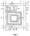
- Fig. 2 is a plan view showing a display pixel and nearby area of an example of the above mentioned reflective type LCD. Fig. 3 is a cross sectional view, along the line A-A in Fig. 2, showing manufacturing steps.
- As shown in Fig. 2, a TFT is formed in an area close to a crossing point between a
gate signal line 51 and adrain signal line 52. Thegate signal line 51 includes agate electrode 11 and supplies a gate signal to a gate, while thedrain signal line 52 includes adrain electrode 16 and supplies a drain signal to a drain. Thegate 11 of the TFT is connected to thegate signal line 51. Thedrain 13d is connected to thedrain signal line 52, while thesource 13s is connected to areflection display electrode 28. - The
reflection display electrode 28 preferably has an uneven surface, rather than an even surface, so that incident light can be reflected in multiple directions. With such an arrangement, the display of the reflection type LCD (Liquid Crystal Display) can be observed from a larger area, so that a larger viewing angle can be ensured. - Referring to Figs. 3(a) to 3(d), an example of manufacturing steps for the above described reflection type LCD will be described.
- Step 1 (Fig. 3(a)): on an
insulating substrate 10, there are sequentially formed afirst gate electrode 11, a gateinsulating film 12, and anactive layer 13, wherein theinsulating substrate 10 comprises a quartz glass, a non-alkali glass, and so on, thefirst gate electrode 11 comprises a refractory metal (Cr, Mo, and so on), the gateinsulating film 12 comprises a SiN film and a SiO2 film, and theactive layer 13 comprises an island-shaped polycrystalline silicon film. - Then, in the
active layer 13, there are formed achannel 13c above thefirst gate electrode 11, and asource 13s and adrain 13d at the respective sides of thechannel 13c, wherein thesource 13s and thedrain 13d are formed through ion implantation. - Further, on the
channel 13c, there is formed astopper insulating film 14, comprising a SiO2 film, as a mask covering thechannel 13c for preventing ion intrusion at the time of ion implantation. - Covering the entire surface of the
gate insulating film 12, theactive layer 13, and thestopper insulating film 14, there is formed aninterlayer insulating film 15, comprising laminated SiO2 film, SiN film and SiO2 film. - Then,
contact holes interlayer insulating film 15 at respective positions corresponding to thedrain 13d and thesource 13s. Thecontact hole 16, corresponding to thedrain 13d, is filled by metal, specifically, by a single Al layer or sequentially laminated Mo and Al layers, thereby forming adrain electrode 18. At the same time of the formation of thedrain electrode 18, asecond gate electrode 19 is formed on theinterlayer insulating film 15 above thechannel 13c using metal, specifically, a single Al layer or sequentially laminated Mo and Al layers. Note that nothing is filled in thecontact hole 17. - The
second gate electrode 19 is connected to thegate signal line 51 on theinsulating substrate 10, via acontact hole 20, formed in thegate insulating film 12 and theinterlayer insulating film 15 as shown in Fig. 1. Adrain signal line 52 is formed on theinterlayer insulating film 15. - Step 2 (Fig. 3(b)): a first
planarization insulating film 21, made of organic resin, and so on, is formed over the layers formed at Step 1, and a first resist film 22 is applied thereon. Thereafter, exposure and development processes are applied using a first mask 23, which has an opening at a position corresponding to thecontact hole 17, followed by etching the firstplanarization insulating film 21, thereby forming acontact hole 24 corresponding to thecontact hole 17. - Step 3 (Fig. 3(c)): a second
planarization insulating film 25 is formed on thesemiconductor film 13 in thecontact hole 24 and the exposed firstplanarization insulating film 21. Asecond resist film 26 is then applied on thefilm 25. Thereafter, exposure and development processes are applied using asecond mask 32, which has an opening at a position corresponding to a recess 27 (29) which is to be formed on an area, on the secondplanarization insulating film 25, where areflection display electrode 28 is to be formed, and the secondplanarization insulating film 25 is thereafter etched whereby a concave 29 (27) is formed (Fig. 3(d)). - With the
second resist film 26 subsequently removed, acontact hole 24, where thereflection display electrode 28 contacts thesource 13s, is formed, and so are concaves 29 (27) in the reflection display electrode formation area. With the above, thereflection display electrode 28 resultantly has an uneven surface. As a result, incident light can be reflected in multiple directions, and a wider viewing angle can thus be achieved. - However, the above described manufacturing method of a reflection type LCD may result in increased costs and labor as it initially requires formation of a
contact hole 24 in the firstplanarization insulating film 21, and then formation of a secondplanarization insulating film 25 in a different manufacturing step for subsequent formation of a concave 29 (27) therein. - The present invention aims to provide an efficient method for manufacturing a reflection type LCD having a concave in a reflection film.
- According to the present invention, two exposures are applied to a photosensitive resin, using two different masks, before development, whereby two types of concaves each having different depths are formed. This enables reduction of the number of steps in formation of concave with two different depths.
- In particular, a concave with one of the two depths is used to constitute a contact hole for connection between a TFT transistor and a reflection film (a reflection electrode) having a size corresponding to a pixel, and a concave with another depth is used as a concave in the reflection electrode.
- The above and other objects, features, and advantages of the present invention will become further apparent from the following description of the preferred embodiment taken in conjunction with the accompanying drawings wherein:
- Figs. 1(a), 1(b), 1(c), 1(d), 1(e) are cross sectional views showing manufacturing steps for a reflection type LCD in a preferred embodiment of the present invention;
- Fig. 2 is a plan view showing a reflection type LCD in the preferred embodiment of the present invention;
- Figs. 3(a), 3(b), 3(c), 3(d) are cross sectional view showing manufacturing steps for a conventional reflection type LCD; and
- Figs. 4(a), 4(b), 4(c), 4(d), 4(e) are cross sectional view showing manufacturing steps for a reflection type LCD in another preferred embodiment of the present invention.
-
- In the following, a manufacturing method for a reflection type LCD according to the present invention will be described.
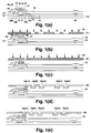
- Figs. 1(a) to 1(e) are cross sectional views, along the line A-A in Fig. 2, showing manufacturing steps for a reflection type LCD of the present invention.
- As shown in Fig. 2, a TFT is formed in an area close to a crossing point between a
gate signal line 51 and adrain signal line 52. Thegate signal line 51 includes afirst gate electrode 11, while thedrain signal line 52 includes adrain electrode 16. Areflection display electrode 28, which comprises reflection material, is connected to the TFT. Thereflection display electrode 28 is provided extending above the TFT, and has a surface with concaves 27 formed thereon. - Step 1 (Fig. 1(a)): on an
insulating substrate 10, there are sequentially formed afirst gate electrode 11, a gateinsulating film 12, and anactive layer 13, wherein theinsulating substrate 10 comprises a quartz glass, a non-alkali glass, and so on, thefirst gate electrode 11 constitutes a part of thegate signal line 51 and comprises refractory metal (Cr, Mo, and so on), the gateinsulating film 12 comprises a SiN film and a SiO2 film, and theactive layer 13 comprises a polycrystalline silicon film. - In the
active layer 13, there are formed achannel 13c above thefirst gate electrode 11, and asource 13s and adrain 13d at the respective sides of thechannel 13c. Thesource 13s and thedrain 13d are formed through ion implantation. - On the
channel 13c, there is formed astopper insulating film 14, comprising a SiO2 film, as a mask covering thechannel 13c for preventing ion intrusion at the time of ion implantation. - Covering the entire surface of the
gate insulating film 12, theactive layer 13, and thestopper insulating film 14, there is formed aninterlayer insulating film 15, which comprises laminated SiO2 film, SiN film and SiO2 film. Theinterlayer insulating film 15 may be formed of either a single layer of organic material such as SiO, SiN, acrylic, and so on, or multiple layers of combinations of any thereof. - Then,
contact holes interlayer insulating film 15 at respective positions corresponding to thedrain 13d and thesource 13s. Thecontact hole 16, corresponding to thedrain 13d, is filled by metal, specifically, by a single Al layer or sequentially laminated Mo and Al layers, thereby forming adrain electrode 18. At the same time as formation of thedrain electrode 18, asecond gate electrode 19 is formed on theinterlayer insulating film 15 above thechannel 13c. That is, asecond gate electrode 19 is formed using metal such as a single Al layer or laminated Mo and Al layers. - The
second gate electrode 19 is connected to thegate signal line 51 on the insulatingsubstrate 10, via acontact hole 20, formed in thegate insulating film 12 and theinterlayer insulating film 15. - A
drain signal line 52 is formed on theinterlayer insulating film 15 at the same time as formation of thedrain electrode 18, which constitutes a part of thedrain signal line 52. - Step 2 (Fig. 1(b)): a
photosensitive resin film 70, made of insulating resin having photosensitivity and an even surface, is formed over the entire surface of theinterlayer insulating film 15, including thecontact hole 17, thedrain signal line 52, thedrain electrode 18, and thesecond gate electrode 19. Thereafter, afirst mask 71 having an opening at a position corresponding to arecess 27 to be formed on an area where areflection display electrode 28 is to be formed, is placed beforefirst exposure 75 is applied. The amount of exposure is determined such that the light reaches a point at a shallow depth below the surface of thephotosensitive resin 70, specifically, 20 mJ/cm2 to 60 mJ/cm2, preferably 25 mJ/cm2 to 50 mJ/cm2, and more preferably 30 mJ/cm2 to 40 mJ/cm2. - Note that specific examples of photosensitive resin may be acrylic resin or polyimide.
- Step 3 (Fig. 1(c)): the
first mask 71 is removed, and asecond mask 72 is placed instead. Thesecond mask 72 has an opening at a position corresponding to a place where acontact hole 73 for connection between thesource 13s of theactive layer 13 and thereflection display electrode 28 is to be formed. - After the deposition of the
second mask 72,second exposure 76 is applied. The amount of the second exposure is larger than that for the first exposure so that adeeper contact hole 73 than the concave 74 can be formed. That is, in order for the exposure light to reach deeper, specifically, deep enough to form acontact hole 73 reaching thesource 13s, the amount ofsecond exposure 76 must be large enough, specifically, 200 mJ/cm2 to 600 mJ/cm2, preferably 250 mJ/cm2 to 500 mJ/cm2, more preferably, 300 mJ/cm2 to 400 mJ/cm2. - Step 4 (Fig. 1(d)): after the
second mask 72 is removed, thephotosensitive resin film 70 is developed whereby a concave 74 and acontact hole 73 are formed. - After the formation of the concave 74 and the
contact hole 73 as described above, areflection display electrode 28, made of reflection material such as Al, is formed thereon. With the above, the contact hole 17 (corresponding to 73 in Fig. 1) and the concave 27 (corresponding to 74 in Fig. 1) are completed. - In addition, an alignment layer for aligning liquid crystal is formed on the
reflection display electrode 28. Formation of the alignment film completes a TFT substrate. Then, opposing the TFT substrate, an opposing electrode substrate is formed, which has an opposing electrode and an alignment layer formed on the side thereof having liquid crystal, and a retardation film and a polarizer formed on the other side thereof without liquid crystal (i.e., on the observer side). The TFT substrate and the opposing electrode substrate are attached to each other along the edges thereof and liquid crystal is filled into the space between them, so that a reflection type LCD is completed. - It should be noted that the opposing electrode substrate is substantially transparent, and is not segmented for every pixel.
- As described above, the use of photosensitive resin and exposure with the photosensitive resin using different amounts of light for formation of a desired contact hole and a concave, readily enable formation of a contact hole and a concave without the need of two formations of a planarization insulating film, as is conventionally needed. Therefore, the manufacturing process can be simplified, and costs can be reduced.
- It should be noted that the present invention is not limited to the above embodiment, in which a concave and a contact hole are formed by development. Moreover, heating at, e.g., about 220 °C after the development would make more gently slanting edges of the concave 74, as shown in Fig. 1 (e), so that a brighter display with incident light reflected in many more different directions can be obtained.
- Also, the present invention is not limited to the above embodiment, in which concaves 27 are formed as two analogous rectangles formed in a reflection display electrode formation area, and the concave 27 may rather be formed in a circle or in two or more different shapes instead. Moreover, the number of the concave 27 is not limited to two, as described above, and a single concave 27 or three or more concaves 27 may be formed instead.
- Further, the area where the concave 27 is formed is not limited to an area enclosed by the
gate signal line 51 and thedrain signal line 52, and the concave 27 may rather be formed in an area overlapping thegate signal line 51 or thedrain signal line 52. - Still further, the present invention is not limited to the above embodiment, in which the circumferential edges of adjacent
reflection display electrodes 28 overlap thegate signal line 51 and thedrain signal line 52, and the edge may rather overlap either one of thegate signal line 51 and thedrain signal line 52 or may even not overlap the signal line. Yet further, thereflection display electrode 28 may not extend over the TFT. - Moreover, the insulating film between the
second gate electrode 17 and theactive layer 13, i.e., thestopper insulating film 14, theinterlayer insulating film 15, and theplanarization insulating film 19 in this embodiment, may each be constituted of a single SiO, SiN, or any organic film, or a laminated combination thereof. - Also, instead of the above described TFT having a double gate electrode structure, having two gates, a single gate structure, having one gate, or a multiple gate structure, having two or more gates, may be similarly applicable.
- The order of formation of the
contact hole 72 and therecess 74 may be reversed from that shown in Figs. 1(a) to 1(e), into that shown in Figs. 4(a) to 4(e). With the reversed order, exposure for formation of thecontact hole 73, as shown in Fig. 4(b), is initially applied, followed by exposure for formation of therecess 74, as shown in Fig. 4(c). In this case, Figs. 4(a), 4(d), 4(e) are identical to Figs. 1(a), 1(d), 1(e), Fig. 4(b) is identical to Fig. 1(c), and Fig. 4(c) is identical to Fig. 1(b). - As described above, according to the present invention, the number of formation steps may be reduced to readily attain contact between the reflection display electrode and the source, while a recess can be formed in a reflection display electrode formation area.
Claims (5)
- A manufacturing method for a reflection type liquid crystal display having a reflection film for reflecting light having passed through a liquid crystal layer, comprising the steps of:forming a photosensitive resin film on a substrate;exposing the photosensitive resin film with a first amount of light via a first mask;exposing the photosensitive resin film with a second amount of light via a second mask;developing the photosensitive resin film subjected to two exposures thereby forming two types of concaves having different depths; andforming a film using reflective material on the photosensitive resin developed to have two types of concaves, thereby forming the reflection film.
- A manufacturing method according to claim 1, further comprising the step of forming a thin film transistor on the substrate so that the photosensitive resin film is formed thereon,
whereinthe photosensitive resin film constitutes an insulating film,the reflection film is a reflection electrode having a size corresponding to a pixel, andthe reflection electrode is electrically connected to the thin film transistor. - A manufacturing method according to claim 2, whereinthe first amount of light is larger than the second amount of light,the concave formed using the first mask constitutes a contact hole for electrically connecting the reflection electrode and the thin film transistor, andthe concave formed using the second mask constitutes a concave formed on a surface of the reflection electrode.
- A manufacturing method according to claim 2, whereinthe second amount of light is larger than the first amount of light,the concave formed using the first mask constitutes a concave formed on a surface of the reflection electrode, andthe concave formed using the second mask constitutes a contact hole for electrically connecting the reflection electrode and the thin film transistor.
- A manufacturing method according to any one of claims 1 to 4, further comprising
after the step of developing the photosensitive resin film, a step of heating to give edges of the concave a gentler slope.
Applications Claiming Priority (2)
| Application Number | Priority Date | Filing Date | Title |
|---|---|---|---|
| JP20060099 | 1999-07-14 | ||
| JP20060099 | 1999-07-14 |
Publications (2)
| Publication Number | Publication Date |
|---|---|
| EP1069458A2 true EP1069458A2 (en) | 2001-01-17 |
| EP1069458A3 EP1069458A3 (en) | 2004-03-10 |
Family
ID=16427068
Family Applications (1)
| Application Number | Title | Priority Date | Filing Date |
|---|---|---|---|
| EP00305867A Withdrawn EP1069458A3 (en) | 1999-07-14 | 2000-07-12 | Manufacturing method for reflection type liquid crystal display |
Country Status (5)
| Country | Link |
|---|---|
| US (1) | US6410358B1 (en) |
| EP (1) | EP1069458A3 (en) |
| JP (1) | JP2001083506A (en) |
| KR (1) | KR100385762B1 (en) |
| TW (1) | TWI224227B (en) |
Cited By (3)
| Publication number | Priority date | Publication date | Assignee | Title |
|---|---|---|---|---|
| US6274886B1 (en) * | 1998-08-31 | 2001-08-14 | Lg. Philips Lcd Co., Ltd. | Thin-film-transistor-array substrate and liquid-crystal display device |
| GB2362509A (en) * | 1999-11-16 | 2001-11-21 | Nec Corp | Thin film transistor (TFT) with front and back channel gates connected together |
| US7692740B2 (en) | 2002-05-30 | 2010-04-06 | Sharp Kabushiki Kaisha | Liquid crystal display having a reflective electrode formed on an organic resin film |
Families Citing this family (11)
| Publication number | Priority date | Publication date | Assignee | Title |
|---|---|---|---|---|
| KR100306546B1 (en) * | 1998-09-28 | 2001-11-02 | 마찌다 가쯔히꼬 | Method of manufacturing liquid crystal display apparatus |
| AUPQ385899A0 (en) * | 1999-11-04 | 1999-11-25 | Pacific Solar Pty Limited | Formation of contacts on thin films |
| JP2002333608A (en) * | 2001-05-09 | 2002-11-22 | Toshiba Corp | Liquid crystal display device and manufacturing method therefor |
| US20020177079A1 (en) * | 2001-05-23 | 2002-11-28 | Chung-Yuan Liu | Method of manufacturing a reflector |
| KR100635039B1 (en) * | 2001-08-17 | 2006-10-17 | 삼성에스디아이 주식회사 | A triodic rectifier switch device and a method for preparation thereof |
| KR100813027B1 (en) * | 2001-08-18 | 2008-03-14 | 삼성전자주식회사 | Methods for forming photosensitive insulating film pattern and reflection electrode each having irregular upper surface and method for manufacturing LCD having reflection electrode using the same |
| KR20030044518A (en) * | 2001-11-30 | 2003-06-09 | 에이유 오프트로닉스 코퍼레이션 | A process for manufacturing reflective tft-lcd with rough diffuser |
| KR100987711B1 (en) * | 2003-11-18 | 2010-10-13 | 삼성전자주식회사 | Liquid crystal display and manufacturing Method thereof |
| JP4693781B2 (en) * | 2004-11-17 | 2011-06-01 | シャープ株式会社 | Active matrix substrate and display device |
| WO2009063684A1 (en) | 2007-11-16 | 2009-05-22 | Sharp Kabushiki Kaisha | Liquid crystal display device |
| KR101534008B1 (en) | 2008-08-12 | 2015-07-07 | 삼성디스플레이 주식회사 | Thin film transistor array panel and manufacturing method thereof |
Citations (3)
| Publication number | Priority date | Publication date | Assignee | Title |
|---|---|---|---|---|
| JPH09127553A (en) * | 1995-10-31 | 1997-05-16 | Sharp Corp | Transmission type liquid crystal display device and its production |
| JPH10221704A (en) * | 1997-02-07 | 1998-08-21 | Sharp Corp | Reflection type liquid crystal display device and its manufacture |
| JPH11183714A (en) * | 1997-12-22 | 1999-07-09 | Sharp Corp | Manufacture of reflection plate, reflection plate and reflection type liquid crystal display device |
Family Cites Families (11)
| Publication number | Priority date | Publication date | Assignee | Title |
|---|---|---|---|---|
| EP0112417A1 (en) | 1982-12-22 | 1984-07-04 | International Business Machines Corporation | Semiconductor integrated display and method of making same |
| DE69331162T2 (en) | 1992-06-26 | 2002-06-20 | Sharp Kk | Reflective liquid crystal display device |
| JP2530990B2 (en) * | 1992-10-15 | 1996-09-04 | 富士通株式会社 | Method of manufacturing thin film transistor matrix |
| JPH0736030A (en) * | 1993-07-23 | 1995-02-07 | Sharp Corp | Reflection type liquid crystal display device |
| US5691791A (en) | 1993-07-30 | 1997-11-25 | Sharp Kabushiki Kaisha | Reflective liquid crystal display device and reflector |
| JP3097945B2 (en) | 1994-10-03 | 2000-10-10 | シャープ株式会社 | Method for manufacturing reflective liquid crystal display device |
| JP2768313B2 (en) | 1995-06-13 | 1998-06-25 | 日本電気株式会社 | Reflective liquid crystal display |
| JP3167605B2 (en) | 1995-12-25 | 2001-05-21 | シャープ株式会社 | Liquid crystal display device |
| JP3898293B2 (en) * | 1997-07-30 | 2007-03-28 | シチズン時計株式会社 | Manufacturing method of liquid crystal device |
| US6037084A (en) * | 1998-08-12 | 2000-03-14 | Industrial Technology Research Institute | Method of making a color filter plate with multi-gap for LCD |
| US6163405A (en) * | 1999-04-15 | 2000-12-19 | Industrial Technology Research Institute | Structure of a reflection-type light diffuser in a LCD |
-
2000
- 2000-06-28 TW TW089112675A patent/TWI224227B/en not_active IP Right Cessation
- 2000-07-12 EP EP00305867A patent/EP1069458A3/en not_active Withdrawn
- 2000-07-13 KR KR10-2000-0040061A patent/KR100385762B1/en not_active IP Right Cessation
- 2000-07-13 JP JP2000212881A patent/JP2001083506A/en active Pending
- 2000-07-14 US US09/615,608 patent/US6410358B1/en not_active Expired - Lifetime
Patent Citations (3)
| Publication number | Priority date | Publication date | Assignee | Title |
|---|---|---|---|---|
| JPH09127553A (en) * | 1995-10-31 | 1997-05-16 | Sharp Corp | Transmission type liquid crystal display device and its production |
| JPH10221704A (en) * | 1997-02-07 | 1998-08-21 | Sharp Corp | Reflection type liquid crystal display device and its manufacture |
| JPH11183714A (en) * | 1997-12-22 | 1999-07-09 | Sharp Corp | Manufacture of reflection plate, reflection plate and reflection type liquid crystal display device |
Non-Patent Citations (3)
| Title |
|---|
| PATENT ABSTRACTS OF JAPAN vol. 1997, no. 09, 30 September 1997 (1997-09-30) -& JP 09 127553 A (SHARP CORP), 16 May 1997 (1997-05-16) -& US 5 946 065 A (TAGUSA ET AL.) 31 August 1999 (1999-08-31) * |
| PATENT ABSTRACTS OF JAPAN vol. 1998, no. 13, 30 November 1998 (1998-11-30) -& JP 10 221704 A (SHARP CORP), 21 August 1998 (1998-08-21) -& US 6 172 728 B1 (HIRAISHI) 9 January 2001 (2001-01-09) * |
| PATENT ABSTRACTS OF JAPAN vol. 1999, no. 12, 29 October 1999 (1999-10-29) -& JP 11 183714 A (SHARP CORP), 9 July 1999 (1999-07-09) -& US 5 973 843 A (NAKAMURA) 26 October 1999 (1999-10-26) * |
Cited By (4)
| Publication number | Priority date | Publication date | Assignee | Title |
|---|---|---|---|---|
| US6274886B1 (en) * | 1998-08-31 | 2001-08-14 | Lg. Philips Lcd Co., Ltd. | Thin-film-transistor-array substrate and liquid-crystal display device |
| GB2362509A (en) * | 1999-11-16 | 2001-11-21 | Nec Corp | Thin film transistor (TFT) with front and back channel gates connected together |
| GB2362509B (en) * | 1999-11-16 | 2002-10-09 | Nec Corp | Thin film transistor and fabrication method of the same |
| US7692740B2 (en) | 2002-05-30 | 2010-04-06 | Sharp Kabushiki Kaisha | Liquid crystal display having a reflective electrode formed on an organic resin film |
Also Published As
| Publication number | Publication date |
|---|---|
| KR100385762B1 (en) | 2003-05-28 |
| KR20010015312A (en) | 2001-02-26 |
| TWI224227B (en) | 2004-11-21 |
| EP1069458A3 (en) | 2004-03-10 |
| US6410358B1 (en) | 2002-06-25 |
| JP2001083506A (en) | 2001-03-30 |
Similar Documents
| Publication | Publication Date | Title |
|---|---|---|
| US20170343870A1 (en) | Liquid crystal display device having rectangular-shaped pixel electrodes overlapping with comb-shaped counter electrodes in plan view | |
| WO2017133097A1 (en) | Array substrate, preparation method therefor, and display panel | |
| KR100239778B1 (en) | Lcd device and its manufacturing method | |
| US20060186409A1 (en) | Liquid crystal display device and method for manufacturing the same | |
| US6410358B1 (en) | Manufacturing method for reflection type liquid crystal display | |
| US6970209B2 (en) | Thin film transistor array substrate for a liquid crystal display and method for fabricating the same | |
| JP2004110054A (en) | Thin film transistor substrate for liquid crystal display, its manufacturing method and liquid crystal display | |
| JP3230669B2 (en) | Thin film transistor substrate for liquid crystal display device and method of manufacturing the same | |
| JP2002090742A (en) | Liquid crystal display device | |
| EP1396019B1 (en) | Thin film transistor self-aligned to a light-shield layer | |
| US6521474B2 (en) | Manufacturing method for reflection type liquid crystal display | |
| KR101085138B1 (en) | Method For Fabricating Thin Film Transistor Substrate | |
| KR20070072823A (en) | Method of fabricating pixel structure | |
| US20030043309A1 (en) | Active matrix substrate and manufacturing method thereof | |
| JP2000305114A (en) | Liquid crystal display device and its production | |
| EP1462843B1 (en) | Transflective Display | |
| JP2005331675A (en) | Liquid crystal display and method for manufacturing the liquid crystal display | |
| KR19990026576A (en) | Liquid crystal display using organic insulating film and manufacturing method thereof | |
| JPH0961811A (en) | Liquid crystal panel | |
| US20070154845A1 (en) | Method for fabricating liquid crystal display device | |
| KR101297357B1 (en) | Vertical alignment mode liquid crystal display device | |
| CN107402485B (en) | Array substrate and manufacturing method thereof, liquid crystal display device and manufacturing method thereof | |
| KR20070001548A (en) | Fabrication method of array substrate for liquid crystal display device | |
| EP3654093B1 (en) | Display device including a patterned conductive layer | |
| KR100483525B1 (en) | Manufacturing method of liquid crystal display device using organic insulating film |
Legal Events
| Date | Code | Title | Description |
|---|---|---|---|
| PUAI | Public reference made under article 153(3) epc to a published international application that has entered the european phase |
Free format text: ORIGINAL CODE: 0009012 |
|
| AK | Designated contracting states |
Kind code of ref document: A2 Designated state(s): AT BE CH CY DE DK ES FI FR GB GR IE IT LI LU MC NL PT SE |
|
| AX | Request for extension of the european patent |
Free format text: AL;LT;LV;MK;RO;SI |
|
| PUAL | Search report despatched |
Free format text: ORIGINAL CODE: 0009013 |
|
| AK | Designated contracting states |
Kind code of ref document: A3 Designated state(s): AT BE CH CY DE DK ES FI FR GB GR IE IT LI LU MC NL PT SE |
|
| AX | Request for extension of the european patent |
Extension state: AL LT LV MK RO SI |
|
| 17P | Request for examination filed |
Effective date: 20040907 |
|
| 17Q | First examination report despatched |
Effective date: 20041004 |
|
| AKX | Designation fees paid |
Designated state(s): DE FR GB |
|
| STAA | Information on the status of an ep patent application or granted ep patent |
Free format text: STATUS: THE APPLICATION HAS BEEN WITHDRAWN |
|
| 18W | Application withdrawn |
Effective date: 20060920 |