EP1067599A1 - A method of forming structures with buried oxide regions in a semiconductor substrate - Google Patents
A method of forming structures with buried oxide regions in a semiconductor substrate Download PDFInfo
- Publication number
- EP1067599A1 EP1067599A1 EP99830442A EP99830442A EP1067599A1 EP 1067599 A1 EP1067599 A1 EP 1067599A1 EP 99830442 A EP99830442 A EP 99830442A EP 99830442 A EP99830442 A EP 99830442A EP 1067599 A1 EP1067599 A1 EP 1067599A1
- Authority
- EP
- European Patent Office
- Prior art keywords
- substrate
- region
- silicon
- trenches
- conductivity
- Prior art date
- Legal status (The legal status is an assumption and is not a legal conclusion. Google has not performed a legal analysis and makes no representation as to the accuracy of the status listed.)
- Granted
Links
- 239000000758 substrate Substances 0.000 title claims abstract description 33
- 238000000034 method Methods 0.000 title claims description 35
- 239000004065 semiconductor Substances 0.000 title claims description 4
- VYPSYNLAJGMNEJ-UHFFFAOYSA-N Silicium dioxide Chemical compound O=[Si]=O VYPSYNLAJGMNEJ-UHFFFAOYSA-N 0.000 claims abstract description 30
- XUIMIQQOPSSXEZ-UHFFFAOYSA-N Silicon Chemical compound [Si] XUIMIQQOPSSXEZ-UHFFFAOYSA-N 0.000 claims abstract description 17
- 229910052710 silicon Inorganic materials 0.000 claims abstract description 16
- 239000010703 silicon Substances 0.000 claims abstract description 16
- 235000012239 silicon dioxide Nutrition 0.000 claims abstract description 15
- 239000000377 silicon dioxide Substances 0.000 claims abstract description 15
- 229910021421 monocrystalline silicon Inorganic materials 0.000 claims abstract description 11
- 238000005530 etching Methods 0.000 claims abstract description 10
- 239000012535 impurity Substances 0.000 claims abstract description 9
- 230000015572 biosynthetic process Effects 0.000 claims description 8
- 238000009413 insulation Methods 0.000 claims description 8
- 229910021420 polycrystalline silicon Inorganic materials 0.000 claims description 4
- 239000011810 insulating material Substances 0.000 claims 1
- 230000001590 oxidative effect Effects 0.000 claims 1
- 230000003647 oxidation Effects 0.000 abstract description 6
- 238000007254 oxidation reaction Methods 0.000 abstract description 6
- 238000002513 implantation Methods 0.000 abstract description 5
- 235000012431 wafers Nutrition 0.000 description 16
- BOTDANWDWHJENH-UHFFFAOYSA-N Tetraethyl orthosilicate Chemical group CCO[Si](OCC)(OCC)OCC BOTDANWDWHJENH-UHFFFAOYSA-N 0.000 description 8
- 150000004767 nitrides Chemical class 0.000 description 7
- 238000004519 manufacturing process Methods 0.000 description 4
- 229910052581 Si3N4 Inorganic materials 0.000 description 3
- 238000001312 dry etching Methods 0.000 description 3
- 230000000873 masking effect Effects 0.000 description 3
- HQVNEWCFYHHQES-UHFFFAOYSA-N silicon nitride Chemical compound N12[Si]34N5[Si]62N3[Si]51N64 HQVNEWCFYHHQES-UHFFFAOYSA-N 0.000 description 3
- 229910052787 antimony Inorganic materials 0.000 description 2
- WATWJIUSRGPENY-UHFFFAOYSA-N antimony atom Chemical compound [Sb] WATWJIUSRGPENY-UHFFFAOYSA-N 0.000 description 2
- 239000003989 dielectric material Substances 0.000 description 2
- -1 for example Substances 0.000 description 2
- 230000001681 protective effect Effects 0.000 description 2
- OAICVXFJPJFONN-UHFFFAOYSA-N Phosphorus Chemical compound [P] OAICVXFJPJFONN-UHFFFAOYSA-N 0.000 description 1
- 239000002131 composite material Substances 0.000 description 1
- 238000011109 contamination Methods 0.000 description 1
- 238000000354 decomposition reaction Methods 0.000 description 1
- 239000012212 insulator Substances 0.000 description 1
- 150000002500 ions Chemical class 0.000 description 1
- 239000000463 material Substances 0.000 description 1
- 239000002184 metal Substances 0.000 description 1
- 238000004377 microelectronic Methods 0.000 description 1
- 238000012986 modification Methods 0.000 description 1
- 230000004048 modification Effects 0.000 description 1
- 230000006911 nucleation Effects 0.000 description 1
- 238000010899 nucleation Methods 0.000 description 1
- 230000003071 parasitic effect Effects 0.000 description 1
- 229910052698 phosphorus Inorganic materials 0.000 description 1
- 239000011574 phosphorus Substances 0.000 description 1
- 238000000206 photolithography Methods 0.000 description 1
Images


Classifications
-
- H—ELECTRICITY
- H01—ELECTRIC ELEMENTS
- H01L—SEMICONDUCTOR DEVICES NOT COVERED BY CLASS H10
- H01L21/00—Processes or apparatus adapted for the manufacture or treatment of semiconductor or solid state devices or of parts thereof
- H01L21/70—Manufacture or treatment of devices consisting of a plurality of solid state components formed in or on a common substrate or of parts thereof; Manufacture of integrated circuit devices or of parts thereof
- H01L21/71—Manufacture of specific parts of devices defined in group H01L21/70
- H01L21/76—Making of isolation regions between components
- H01L21/762—Dielectric regions, e.g. EPIC dielectric isolation, LOCOS; Trench refilling techniques, SOI technology, use of channel stoppers
- H01L21/76202—Dielectric regions, e.g. EPIC dielectric isolation, LOCOS; Trench refilling techniques, SOI technology, use of channel stoppers using a local oxidation of silicon, e.g. LOCOS, SWAMI, SILO
- H01L21/76205—Dielectric regions, e.g. EPIC dielectric isolation, LOCOS; Trench refilling techniques, SOI technology, use of channel stoppers using a local oxidation of silicon, e.g. LOCOS, SWAMI, SILO in a region being recessed from the surface, e.g. in a recess, groove, tub or trench region
- H01L21/76208—Dielectric regions, e.g. EPIC dielectric isolation, LOCOS; Trench refilling techniques, SOI technology, use of channel stoppers using a local oxidation of silicon, e.g. LOCOS, SWAMI, SILO in a region being recessed from the surface, e.g. in a recess, groove, tub or trench region using auxiliary pillars in the recessed region, e.g. to form LOCOS over extended areas
-
- H—ELECTRICITY
- H01—ELECTRIC ELEMENTS
- H01L—SEMICONDUCTOR DEVICES NOT COVERED BY CLASS H10
- H01L21/00—Processes or apparatus adapted for the manufacture or treatment of semiconductor or solid state devices or of parts thereof
- H01L21/70—Manufacture or treatment of devices consisting of a plurality of solid state components formed in or on a common substrate or of parts thereof; Manufacture of integrated circuit devices or of parts thereof
- H01L21/71—Manufacture of specific parts of devices defined in group H01L21/70
- H01L21/76—Making of isolation regions between components
- H01L21/763—Polycrystalline semiconductor regions
Definitions
- a particular object of the present invention is to propose a method which enables high-performance devices with dielectric insulation and buried regions to be formed.
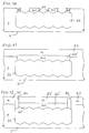
- the polycrystalline silicon layer 52 is partially removed by dry etching and is then oxidized so as to form a silicon dioxide insert 53 in the mouth of the channel 50 until the channel is closed ( Figure 14).
Abstract

Description
- The present invention relates to the manufacture of semiconductor devices and, more particularly, to a method of forming a structure with buried regions in a semiconductor device.
- In the design of integrated circuits, there is often a need to produce components having different electrical characteristics, for example, power transistors, diodes with high reverse-breakdown voltages, signal transistors for signal-processing units and control units. There is a particular need for very good insulation from the substrate, particularly for components of some types, to prevent parasitic currents and interference with the operation of the integrated circuit. For these components, it is often very helpful to use techniques which enable insulating layers of dielectric material to be formed. One of these techniques is based on the use of SOI (silicon on insulator) wafers, that is, composite wafers constituted by two layers of silicon, one thicker layer which acts as a support and one thinner layer in which the components of the integrated circuit are formed, the layers being separated by a layer of silicon dioxide. For other components, for example, power transistors with vertical conduction, it is necessary to use a wafer constituted by a substrate of monocrystalline silicon covered by a thin silicon layer produced by epitaxial growth.
- A method of manufacturing SOI wafers is the subject of European patent application 98830007.5 filed on 13.01.98 in the name of SGS-Thomson Microelectronics S.r.l. The main steps of this method are common to the method of the present invention and will therefore be described below in the course of the description of an embodiment of the invention. This known method was designed to be used mainly to produce an SOI structure which extends throughout the wafer but may also be used to produce an SOI structure on only a portion of the wafer. It is therefore suitable for the production of integrated circuits comprising both power components with vertical conduction and components with good insulation, that is, with practically zero leakage currents to the substrate.
- A component with good insulation which can be produced by this method is shown in Figure 1. In particular, Figure 1 shows, in section, a portion of a wafer containing a diode.
- The wafer comprises a
substrate 10 of monocrystalline silicon with p-type conductivity and anepitaxial layer 11 formed on thesubstrate 10. Asilicon dioxide plaque 12 separates a portion of theepitaxial layer 11 from the substrate. A diffusedplanar region 13 with p-type conductivity and with low resistivity (and hence indicated p+) extends from the front surface of the wafer as far as theoxide plaque 12 in the form of a ring or frame inside which an epitaxial region 11' is defined. Two planar regions, that is, a p-type region 14 and an n-type region with low resistivity (and hence indicated n+) are formed in this epitaxial region and each has, on the surface, a contact electrode with the function of an anode terminal A and of a cathode terminal K of the diode, respectively. The diode is insulated from thesubstrate 10 very effectively but has a considerable resistance when it is biased for direct conduction because of the relatively high resistivity of the epitaxial region 11'. - A usual method of reducing this resistance is to form a buried n-type layer of low resistivity by implantation of a high dose of doping ions before the growth of the epitaxial layer. With the known method, however, the growth of the epitaxial layer on the portion of the wafer in which the oxide plaque has been formed takes place on a discontinuous surface partly of silicon and partly of oxide so that it is a critical operation per se (this processing step according to the known method will also be described below since it is common to the known method and the method according to the invention). Implantation at this point would not be advisable because it would lead to unacceptable contamination of the oxide of the
plaque 12 or would require masking operations which would complicate the method considerably. - The general object of the present invention is to propose a method by which it is possible to form integrated circuits comprising components of different types including components which are completely insulated from the substrate and which have a low resistance during direct conduction.
- A particular object of the present invention is to propose a method which enables high-performance devices with dielectric insulation and buried regions to be formed.
- These objects are achieved by the provision of the method defined in the first claim.
- The invention will be understood further from the following detailed description of a non-limiting embodiment, given with reference to the appended drawings, in which:
- Figure 1 shows, in section, a portion of a wafer comprising an insulated device formed by the method described in the patent application cited above, and
- Figures 2 to 15 show, in section, a portion of a wafer at various stages of processing in accordance with the method of the invention.
-
- The method according to the invention starts with the formation, on a major flat surface of a
monocrystalline silicon substrate 2 with p-type conductivity and resistivity of 0.01 - 150 ohm.cm, of amask 40 of material resistant to implantation, for example, resist, having anopening 41. Doping impurities are implanted in thesubstrate 2 with a high dose through this opening, for example, antimony (Sb) is implanted with a dose of 2.5·1015 atoms/cm2 and an energy of 80 Kev (Figure 2). After the removal of themask 40, with subsequent high-temperature treatment (for example 1250°C for 4 hours), the impurities diffuse in thesubstrate 2 and form aregion 42 with low resistivity (about 15 - 20·10-3 ohm.cm) (Figure 3) which extends to a depth of about 10 µm. - A first layer of silicon dioxide with a thickness, for example, of between 20 and 60 nm is formed by thermal oxidation on the
front surface 3 of thesubstrate 2, at least on theregion 42; a first layer of silicon nitride with a thickness of between 90 and 150 nm and a second layer of silicon dioxide, produced by decomposition of tetraethyl orthosilicate (TEOS) and having a thickness of between 100 and 600 nm, are then deposited thereon. A structure, for example with rectangular areas, is defined in plan with the use of a resist layer and a masking operation. Dry etching of the exposed portions of the oxide layer produced from TEOS, of the first nitride layer, and of the first oxide layer is then performed and the residual resist is then removed, producing the structure shown in section in Figure 4. The portions of the first oxide layer, of the first nitride layer, and of the oxide layer produced from TEOS which remain after the dry etching are indicated 4, 5 and 6, respectively and together defineprotective plaques 7 covering portions 8' of themonocrystalline silicon substrate 2. - The
protective plaques 7 form a mask, generally indicated 9, for subsequent selective anisotropic etching of thesilicon substrate 2. The portions of thesubstrate 2 which are indicated 8'' in Figure 4, and which are not protected by themask 9 are etched by this treatment so thatinitial trenches 10 are formed (Figure 5). - Then, as shown by Figure 6, the structure is subjected to an oxidation step leading to the formation of a third
silicon dioxide layer 11 which has a thickness, for example, of between 20 and 60 nm and which covers the walls and the base of theinitial trenches 10. A secondsilicon nitride layer 12 with a thickness of between 90 and 150 nm is then deposited. - The method continues with dry anisotropic etching during which the horizontal portions of the second
silicon nitride layer 12 are removed. During this etching, thefirst nitride layer 5 is protected by theoxide layer 6 produced from TEOS. Thethird oxide layer 11 which is disposed in the bases of theinitial trenches 10 is removed in a wet process. The structure shown in Figure 7, which shows the portions 8' still covered at the top by themask 9 and at the sides (on the vertical walls of the initial trenches 10) by oxide and nitride portions 11' and 12', respectively, and the exposedbases 15 of theinitial trenches 10, is thus produced. - Anisotropic etching of the silicon is then performed with the use, as a mask, of the
mask 9 modified by the addition of the oxide and nitride portions 11' and 12', respectively. The exposed silicon in thebases 15 of theinitial trenches 10 is etched for sufficient time to producefinal trenches 16 which extend in depth beyond the boundary of then+ region 42. It will be noted that the difference between the depth of thefinal trenches 16 and that of theinitial trenches 10 determines the dimensions of the buried oxide layer, as will become clearer from the following. The depth of etching is therefore selected on the basis of the specification of the SOI wafer to be produced. - The monocrystalline silicon substrate thus treated is now formed by a base portion indicated 2' and by a plurality of "pillars" 18 of rectangular cross-section extending from the base portion 2' towards the surface of the wafer. That is, the structure shown in Figure 8 is produced, in which the
nitride portions 5 and 12' are no longer distinct from one another and are together indicated 19 and theoxide portions 4 and 11' are together indicated 20. Theportions overlying portions 6 of oxide produced from TEOS together constitute amask 30. - The silicon substrate is then subjected to selective oxidation, with the use of the
mask 30 for protecting the silicon from oxidation as far as a predetermined distance d from the surface of the substrate. The process continues until the portions of thepillars 18 which are not protected by themask 30 are completely transformed into silicon dioxide. In practice, a gradual growth of the oxide regions takes place at the expense of the silicon regions, starting from the side walls of thefinal trenches 16 towards the interiors of thepillars 18 and also partially into the base portion 2'. Since the volume of the silicon dioxide which is formed is greater than that of the starting silicon, the oxide regions being formed gradually take up the space in thefinal trenches 16 until these are completely closed and joined together. The oxidation step finishes automatically when thepillars 18 are completely oxidized (naturally apart from their tops, indicated 21, which are protected by the mask 30). An oxide region orplaque 22 which is buried to a large extent is thus formed, as shown in Figure 9. - The
oxide portions 6 produced from TEOS, thenitride portions 19 and theoxide portions 20 which constitute themask 30 are then removed by selective etching so as to expose thetops 21 which are to form seeds for subsequent epitaxial growth, and the rest of the surface of the substrate. The resulting structure is shown in Figure 10. - The epitaxial growth is performed from a vapour phase, the operative parameters being selected in a manner such as to prevent nucleation of polycrystalline silicon in the exposed zones of the buried
oxide region 22 and in a manner such that the lateral/vertical growth ratio is high. A growth of the silicon in a lateral direction around thetops 21 is thus achieved first of all, until the portions of the trenches which are still open are filled, with the subsequent growth of an epitaxial layer in a direction perpendicular to the major surface of the substrate. During the epitaxial growth, which takes place at a temperature of between 900 and 1230°C and has a duration of 15 minutes, the doping impurities (antimony in this example) which are present in what remains of theregion 42 diffuse into the epitaxial layer being formed so as to form a homogeneous buried region. Naturally, the dose of the initial implantation (Figure 2) is determined in a manner such that this buried region has the desired resistivity. The epitaxial growth preferably takes place in an atmosphere containing doping impurities, for example, phosphorus, so that the epitaxial layer has the same type of conductivity as the buried region and a greater resistivity (for example 1.1 - 1.6 ohm.cm). - After an optional chemical-mechanical lapping step to flatten the surface of the epitaxial layer, the final structure shown in Figure 11 is produced, in which the buried region is indicated 42' and the residual epitaxial layer is indicated 23.
- All of the usual components necessary to form the integrated circuit can now be formed in the
epitaxial layer 23. Moreover, by virtue of the method according to the invention, it is easy to produce components which are free of current leakages towards the substrate and which have very low resistance during direct conduction. As an example of such a component, the main steps for the production of a diode which, owing to its optimal characteristics of insulation and resistance during conduction, may form part, for example, of a high-performance diode bridge in an integrated circuit for controlling an electric motor, are described below. - In order to insulate the diode laterally, the usual junction insulation technique may be used, as in the example described with reference to Figure 1, or a technique of insulation with dielectric, which is more advantageous in terms of electrical performance and area occupied, may be used. A technique of this latter type is described herein with reference to Figures 12 to 15.
- A
channel 50 which extends from the surface of theepitaxial layer 23 to theoxide plaque 22 and is shaped as a ring or a frame so as to enclose within it a portion 23' of theepitaxial layer 23 with the underlying buried layer 42' is hollowed out by normal masking and anisotropic etching operations (Figure 12). - The surface of the
epitaxial layer 23 and the internal walls of the channel are covered with alayer 51 of dielectric material, for example, silicon dioxide produced from TEOS. Polycrystalline silicon is then deposited so as to fill thechannel 50 and to cover the front surface of the wafer with a layer 52 (Figure 13). - The
polycrystalline silicon layer 52 is partially removed by dry etching and is then oxidized so as to form asilicon dioxide insert 53 in the mouth of thechannel 50 until the channel is closed (Figure 14). - Two planar regions, a p-type region indicated 54 and a n-
type region 55 with low resistivity are formed by usual photolithography, etching and doping techniques. Finally, twometal electrodes regions - Although only one example of the method according to the invention has been described and illustrated, many variations and modifications are possible. For example, the buried layer may be formed on the entire wafer or on an area more extensive than that of the oxide plaque if the integrated circuit requires other components with low resistance during conduction.
Claims (6)
- A method of forming a structure with a buried region in a semiconductor device comprising the following steps:a. providing a monocrystalline silicon substrate (2) with a flat major surface (3),b. introducing doping impurities (Sb) into the substrate through a portion of the major surface (3) of the substrate (2) to a predetermined depth in order to form a planar region (42) with a first type of conductivity (n),c. subjecting the substrate (2) to selective anisotropic etching in order to hollow out trenches (10, 16) in the substrate (2) from the said portion of the major surface (3) to a depth greater than the predetermined depth,d. oxidizing the silicon within the trenches (10, 16), starting a predetermined distance (d) from the major surface of the substrate, until the portions of the substrate between adjacent trenches are transformed into silicon dioxide and until the trenches are filled with silicon dioxide below the level defined by the predetermined distance (d) in order thus to form a silicon dioxide plaque (22),e. subjecting the substrate (2) to a treatment of epitaxial growth from a vapour phase, the operative parameters being selected in a manner such as to permit a growth of monocrystalline silicon both inside the portions of the trenches (10, 16) which are still open until the trenches are closed, and on top of the major surface of the substrate (2), and in a manner such as to permit a redistribution of the doping impurities (Sb) into the monocrystalline silicon grown, to form a region (42') with the first type of conductivity (n), with substantially homogeneous resistivity, buried in an epitaxial layer (23) and extending on the silicon dioxide plaque (42).
- A method according to Claim 1, in which step e. comprises the introduction of doping impurities with the first type of conductivity (n) during the monocrystalline silicon growth.
- A method according to Claim 2, comprising the formation of an insulating frame which extends from the free surface, from the epitaxial layer as far as the silicon dioxide plaque (22), and within which is defined a portion of monocrystalline silicon formed substantially by the buried region (42') and by an epitaxial region (23') with resistivity greater than that of the buried region.
- A method according to Claim 3, in which the formation of an insulating frame comprises the hollowing-out of a channel (50), the covering of the walls of the channel (50) with insulating material (51), and the filling of the channel (50) with polycrystalline silicon (52).
- A method according to Claim 3, in which the formation of an insulating frame comprises the formation of a region with a second type of conductivity (p) for a junction insulation.
- A method according to Claim 4 or Claim 5, comprising the formation of a planar region (54) with the second type of conductivity (p) in the epitaxial region (23'), and of a planar region (55) with the first type of conductivity (n) and with resistivity lower than that of the epitaxial region (23'), and the formation of contact electrodes (56, 57) on the surfaces of these planar regions.
Priority Applications (4)
| Application Number | Priority Date | Filing Date | Title |
|---|---|---|---|
| EP99830442A EP1067599B1 (en) | 1999-07-09 | 1999-07-09 | A method of forming structures with buried oxide regions in a semiconductor substrate |
| DE69937106T DE69937106T2 (en) | 1999-07-09 | 1999-07-09 | Method for producing structures with buried oxide regions in a semiconductor substrate |
| JP2000208131A JP2001044399A (en) | 1999-07-09 | 2000-07-10 | Method for manufacturing semiconductor device |
| US09/613,109 US6455391B1 (en) | 1999-07-09 | 2000-07-10 | Method of forming structures with buried regions in a semiconductor device |
Applications Claiming Priority (1)
| Application Number | Priority Date | Filing Date | Title |
|---|---|---|---|
| EP99830442A EP1067599B1 (en) | 1999-07-09 | 1999-07-09 | A method of forming structures with buried oxide regions in a semiconductor substrate |
Publications (2)
| Publication Number | Publication Date |
|---|---|
| EP1067599A1 true EP1067599A1 (en) | 2001-01-10 |
| EP1067599B1 EP1067599B1 (en) | 2007-09-12 |
Family
ID=8243498
Family Applications (1)
| Application Number | Title | Priority Date | Filing Date |
|---|---|---|---|
| EP99830442A Expired - Lifetime EP1067599B1 (en) | 1999-07-09 | 1999-07-09 | A method of forming structures with buried oxide regions in a semiconductor substrate |
Country Status (4)
| Country | Link |
|---|---|
| US (1) | US6455391B1 (en) |
| EP (1) | EP1067599B1 (en) |
| JP (1) | JP2001044399A (en) |
| DE (1) | DE69937106T2 (en) |
Cited By (4)
| Publication number | Priority date | Publication date | Assignee | Title |
|---|---|---|---|---|
| US6455391B1 (en) | 1999-07-09 | 2002-09-24 | Stmicroelectronics S.R.L. | Method of forming structures with buried regions in a semiconductor device |
| EP1427011A1 (en) * | 2002-12-04 | 2004-06-09 | STMicroelectronics S.r.l. | Method for realizing microchannels in an integrated structure |
| US7294536B2 (en) | 2000-07-25 | 2007-11-13 | Stmicroelectronics S.R.L. | Process for manufacturing an SOI wafer by annealing and oxidation of buried channels |
| CN105074922A (en) * | 2013-06-14 | 2015-11-18 | 富士电机株式会社 | Semiconductor device |
Families Citing this family (3)
| Publication number | Priority date | Publication date | Assignee | Title |
|---|---|---|---|---|
| JP2000058802A (en) * | 1998-01-13 | 2000-02-25 | Stmicroelectronics Srl | Manufacture of soi wafer |
| JP5757145B2 (en) * | 2011-04-19 | 2015-07-29 | 富士電機株式会社 | Semiconductor device |
| CN110858561A (en) * | 2018-08-23 | 2020-03-03 | 合肥晶合集成电路有限公司 | Silicon island structure and manufacturing method thereof |
Citations (6)
| Publication number | Priority date | Publication date | Assignee | Title |
|---|---|---|---|---|
| JPS5612749A (en) * | 1979-07-12 | 1981-02-07 | Matsushita Electric Ind Co Ltd | Production of semiconductor device |
| US4502913A (en) * | 1982-06-30 | 1985-03-05 | International Business Machines Corporation | Total dielectric isolation for integrated circuits |
| US4604162A (en) * | 1983-06-13 | 1986-08-05 | Ncr Corporation | Formation and planarization of silicon-on-insulator structures |
| US4814287A (en) * | 1983-09-28 | 1989-03-21 | Matsushita Electric Industrial Co. Ltd. | Method of manufacturing a semiconductor integrated circuit device |
| US4891092A (en) * | 1986-01-13 | 1990-01-02 | General Electric Company | Method for making a silicon-on-insulator substrate |
| EP0929095A1 (en) * | 1998-01-13 | 1999-07-14 | STMicroelectronics S.r.l. | Method for producing an SOI wafer |
Family Cites Families (2)
| Publication number | Priority date | Publication date | Assignee | Title |
|---|---|---|---|---|
| US5907782A (en) * | 1998-08-15 | 1999-05-25 | Acer Semiconductor Manufacturing Inc. | Method of forming a multiple fin-pillar capacitor for a high density dram cell |
| DE69937106T2 (en) | 1999-07-09 | 2008-06-05 | Stmicroelectronics S.R.L., Agrate Brianza | Method for producing structures with buried oxide regions in a semiconductor substrate |
-
1999
- 1999-07-09 DE DE69937106T patent/DE69937106T2/en not_active Expired - Lifetime
- 1999-07-09 EP EP99830442A patent/EP1067599B1/en not_active Expired - Lifetime
-
2000
- 2000-07-10 US US09/613,109 patent/US6455391B1/en not_active Expired - Lifetime
- 2000-07-10 JP JP2000208131A patent/JP2001044399A/en active Pending
Patent Citations (6)
| Publication number | Priority date | Publication date | Assignee | Title |
|---|---|---|---|---|
| JPS5612749A (en) * | 1979-07-12 | 1981-02-07 | Matsushita Electric Ind Co Ltd | Production of semiconductor device |
| US4502913A (en) * | 1982-06-30 | 1985-03-05 | International Business Machines Corporation | Total dielectric isolation for integrated circuits |
| US4604162A (en) * | 1983-06-13 | 1986-08-05 | Ncr Corporation | Formation and planarization of silicon-on-insulator structures |
| US4814287A (en) * | 1983-09-28 | 1989-03-21 | Matsushita Electric Industrial Co. Ltd. | Method of manufacturing a semiconductor integrated circuit device |
| US4891092A (en) * | 1986-01-13 | 1990-01-02 | General Electric Company | Method for making a silicon-on-insulator substrate |
| EP0929095A1 (en) * | 1998-01-13 | 1999-07-14 | STMicroelectronics S.r.l. | Method for producing an SOI wafer |
Non-Patent Citations (1)
| Title |
|---|
| PATENT ABSTRACTS OF JAPAN vol. 005, no. 063 (E - 054) 28 April 1981 (1981-04-28) * |
Cited By (10)
| Publication number | Priority date | Publication date | Assignee | Title |
|---|---|---|---|---|
| US6455391B1 (en) | 1999-07-09 | 2002-09-24 | Stmicroelectronics S.R.L. | Method of forming structures with buried regions in a semiconductor device |
| US7294536B2 (en) | 2000-07-25 | 2007-11-13 | Stmicroelectronics S.R.L. | Process for manufacturing an SOI wafer by annealing and oxidation of buried channels |
| US7754578B2 (en) | 2001-12-28 | 2010-07-13 | Stmicroelectronics, S.R.L. | Process for manufacturing a wafer by annealing of buried channels |
| US8334188B2 (en) | 2001-12-28 | 2012-12-18 | Stmicroelectronics S.R.L. | Process for manufacturing a wafer by annealing of buried channels |
| EP1427011A1 (en) * | 2002-12-04 | 2004-06-09 | STMicroelectronics S.r.l. | Method for realizing microchannels in an integrated structure |
| US7063798B2 (en) | 2002-12-04 | 2006-06-20 | Stmicroelectronics S.R.L. | Method for realizing microchannels in an integrated structure |
| CN105074922A (en) * | 2013-06-14 | 2015-11-18 | 富士电机株式会社 | Semiconductor device |
| EP3010042A4 (en) * | 2013-06-14 | 2017-01-18 | Fuji Electric Co., Ltd. | Semiconductor device |
| US10002961B2 (en) | 2013-06-14 | 2018-06-19 | Fuji Electric Co., Ltd. | Semiconductor device suppressing current leakage in a bootstrap diode |
| CN105074922B (en) * | 2013-06-14 | 2018-07-03 | 富士电机株式会社 | Semiconductor devices |
Also Published As
| Publication number | Publication date |
|---|---|
| EP1067599B1 (en) | 2007-09-12 |
| JP2001044399A (en) | 2001-02-16 |
| DE69937106T2 (en) | 2008-06-05 |
| US6455391B1 (en) | 2002-09-24 |
| DE69937106D1 (en) | 2007-10-25 |
Similar Documents
| Publication | Publication Date | Title |
|---|---|---|
| EP1043775B1 (en) | Power integrated circuit with vertical current flow and related manufacturing process | |
| US6168996B1 (en) | Method of fabricating semiconductor device | |
| JPH05102296A (en) | Manufacture of shallow trench separation flattened in integrated circuit and constitution body that is fabricated therewith | |
| US5049521A (en) | Method for forming dielectrically isolated semiconductor devices with contact to the wafer substrate | |
| US5856700A (en) | Semiconductor device with doped semiconductor and dielectric trench sidewall layers | |
| US20050145981A1 (en) | Methods for manufacturing SOI substrate using wafer bonding and complementary high voltage bipolar transistor using the SOI substrate | |
| US4992843A (en) | Collector contact of an integrated bipolar transistor | |
| US6599810B1 (en) | Shallow trench isolation formation with ion implantation | |
| US6331470B1 (en) | Process for manufacturing a semiconductor material wafer having power regions dielectrically insulated from circuitry regions | |
| EP1067599B1 (en) | A method of forming structures with buried oxide regions in a semiconductor substrate | |
| US6617646B2 (en) | Reduced substrate capacitance high performance SOI process | |
| JP2000349289A (en) | Semiconductor device and manufacture thereof | |
| US6727569B1 (en) | Method of making enhanced trench oxide with low temperature nitrogen integration | |
| JP2850527B2 (en) | Semiconductor device and manufacturing method thereof | |
| JP3142336B2 (en) | Semiconductor device and manufacturing method thereof | |
| US20030006487A1 (en) | Semiconductor device having element isolation structure | |
| JP3257523B2 (en) | Method for manufacturing semiconductor device | |
| KR100249022B1 (en) | Semiconductor element isolating method | |
| JPH05109884A (en) | Manufacture of semiconductor device | |
| JP2000031489A (en) | Manufacturing semiconductor device | |
| JPS5992546A (en) | Bipolar integrated circuit device | |
| JP2000260780A (en) | Semiconductor device and its manufacture | |
| JPH11233616A (en) | Semiconductor device and its manufacturing method | |
| KR100268866B1 (en) | Semiconductor device and method for fabricating the same | |
| JPH04280423A (en) | Manufacture of semiconductor device |
Legal Events
| Date | Code | Title | Description |
|---|---|---|---|
| PUAI | Public reference made under article 153(3) epc to a published international application that has entered the european phase |
Free format text: ORIGINAL CODE: 0009012 |
|
| AK | Designated contracting states |
Kind code of ref document: A1 Designated state(s): DE FR GB IT |
|
| AX | Request for extension of the european patent |
Free format text: AL;LT;LV;MK;RO;SI |
|
| 17P | Request for examination filed |
Effective date: 20010615 |
|
| AKX | Designation fees paid |
Free format text: DE FR GB IT |
|
| GRAP | Despatch of communication of intention to grant a patent |
Free format text: ORIGINAL CODE: EPIDOSNIGR1 |
|
| GRAS | Grant fee paid |
Free format text: ORIGINAL CODE: EPIDOSNIGR3 |
|
| GRAA | (expected) grant |
Free format text: ORIGINAL CODE: 0009210 |
|
| AK | Designated contracting states |
Kind code of ref document: B1 Designated state(s): DE FR GB IT |
|
| REG | Reference to a national code |
Ref country code: GB Ref legal event code: FG4D |
|
| REF | Corresponds to: |
Ref document number: 69937106 Country of ref document: DE Date of ref document: 20071025 Kind code of ref document: P |
|
| ET | Fr: translation filed | ||
| PLBE | No opposition filed within time limit |
Free format text: ORIGINAL CODE: 0009261 |
|
| STAA | Information on the status of an ep patent application or granted ep patent |
Free format text: STATUS: NO OPPOSITION FILED WITHIN TIME LIMIT |
|
| 26N | No opposition filed |
Effective date: 20080613 |
|
| GBPC | Gb: european patent ceased through non-payment of renewal fee |
Effective date: 20080709 |
|
| PG25 | Lapsed in a contracting state [announced via postgrant information from national office to epo] |
Ref country code: GB Free format text: LAPSE BECAUSE OF NON-PAYMENT OF DUE FEES Effective date: 20080709 |
|
| PG25 | Lapsed in a contracting state [announced via postgrant information from national office to epo] |
Ref country code: IT Free format text: LAPSE BECAUSE OF NON-PAYMENT OF DUE FEES Effective date: 20080709 |
|
| PGFP | Annual fee paid to national office [announced via postgrant information from national office to epo] |
Ref country code: DE Payment date: 20130621 Year of fee payment: 15 |
|
| PGFP | Annual fee paid to national office [announced via postgrant information from national office to epo] |
Ref country code: FR Payment date: 20130722 Year of fee payment: 15 |
|
| REG | Reference to a national code |
Ref country code: DE Ref legal event code: R119 Ref document number: 69937106 Country of ref document: DE |
|
| REG | Reference to a national code |
Ref country code: FR Ref legal event code: ST Effective date: 20150331 |
|
| PG25 | Lapsed in a contracting state [announced via postgrant information from national office to epo] |
Ref country code: DE Free format text: LAPSE BECAUSE OF NON-PAYMENT OF DUE FEES Effective date: 20150203 |
|
| REG | Reference to a national code |
Ref country code: DE Ref legal event code: R119 Ref document number: 69937106 Country of ref document: DE Effective date: 20150203 |
|
| PG25 | Lapsed in a contracting state [announced via postgrant information from national office to epo] |
Ref country code: FR Free format text: LAPSE BECAUSE OF NON-PAYMENT OF DUE FEES Effective date: 20140731 |