EP1063690A1 - Plasma processing apparatus and plasma processing method - Google Patents
Plasma processing apparatus and plasma processing method Download PDFInfo
- Publication number
- EP1063690A1 EP1063690A1 EP99907872A EP99907872A EP1063690A1 EP 1063690 A1 EP1063690 A1 EP 1063690A1 EP 99907872 A EP99907872 A EP 99907872A EP 99907872 A EP99907872 A EP 99907872A EP 1063690 A1 EP1063690 A1 EP 1063690A1
- Authority
- EP
- European Patent Office
- Prior art keywords
- gas
- plasma
- process gas
- chamber
- gas introducing
- Prior art date
- Legal status (The legal status is an assumption and is not a legal conclusion. Google has not performed a legal analysis and makes no representation as to the accuracy of the status listed.)
- Withdrawn
Links
Images


Classifications
-
- C—CHEMISTRY; METALLURGY
- C23—COATING METALLIC MATERIAL; COATING MATERIAL WITH METALLIC MATERIAL; CHEMICAL SURFACE TREATMENT; DIFFUSION TREATMENT OF METALLIC MATERIAL; COATING BY VACUUM EVAPORATION, BY SPUTTERING, BY ION IMPLANTATION OR BY CHEMICAL VAPOUR DEPOSITION, IN GENERAL; INHIBITING CORROSION OF METALLIC MATERIAL OR INCRUSTATION IN GENERAL
- C23C—COATING METALLIC MATERIAL; COATING MATERIAL WITH METALLIC MATERIAL; SURFACE TREATMENT OF METALLIC MATERIAL BY DIFFUSION INTO THE SURFACE, BY CHEMICAL CONVERSION OR SUBSTITUTION; COATING BY VACUUM EVAPORATION, BY SPUTTERING, BY ION IMPLANTATION OR BY CHEMICAL VAPOUR DEPOSITION, IN GENERAL
- C23C16/00—Chemical coating by decomposition of gaseous compounds, without leaving reaction products of surface material in the coating, i.e. chemical vapour deposition [CVD] processes
- C23C16/44—Chemical coating by decomposition of gaseous compounds, without leaving reaction products of surface material in the coating, i.e. chemical vapour deposition [CVD] processes characterised by the method of coating
- C23C16/455—Chemical coating by decomposition of gaseous compounds, without leaving reaction products of surface material in the coating, i.e. chemical vapour deposition [CVD] processes characterised by the method of coating characterised by the method used for introducing gases into reaction chamber or for modifying gas flows in reaction chamber
- C23C16/45563—Gas nozzles
- C23C16/45574—Nozzles for more than one gas
-
- C—CHEMISTRY; METALLURGY
- C23—COATING METALLIC MATERIAL; COATING MATERIAL WITH METALLIC MATERIAL; CHEMICAL SURFACE TREATMENT; DIFFUSION TREATMENT OF METALLIC MATERIAL; COATING BY VACUUM EVAPORATION, BY SPUTTERING, BY ION IMPLANTATION OR BY CHEMICAL VAPOUR DEPOSITION, IN GENERAL; INHIBITING CORROSION OF METALLIC MATERIAL OR INCRUSTATION IN GENERAL
- C23C—COATING METALLIC MATERIAL; COATING MATERIAL WITH METALLIC MATERIAL; SURFACE TREATMENT OF METALLIC MATERIAL BY DIFFUSION INTO THE SURFACE, BY CHEMICAL CONVERSION OR SUBSTITUTION; COATING BY VACUUM EVAPORATION, BY SPUTTERING, BY ION IMPLANTATION OR BY CHEMICAL VAPOUR DEPOSITION, IN GENERAL
- C23C16/00—Chemical coating by decomposition of gaseous compounds, without leaving reaction products of surface material in the coating, i.e. chemical vapour deposition [CVD] processes
- C23C16/44—Chemical coating by decomposition of gaseous compounds, without leaving reaction products of surface material in the coating, i.e. chemical vapour deposition [CVD] processes characterised by the method of coating
- C23C16/455—Chemical coating by decomposition of gaseous compounds, without leaving reaction products of surface material in the coating, i.e. chemical vapour deposition [CVD] processes characterised by the method of coating characterised by the method used for introducing gases into reaction chamber or for modifying gas flows in reaction chamber
- C23C16/45502—Flow conditions in reaction chamber
-
- C—CHEMISTRY; METALLURGY
- C23—COATING METALLIC MATERIAL; COATING MATERIAL WITH METALLIC MATERIAL; CHEMICAL SURFACE TREATMENT; DIFFUSION TREATMENT OF METALLIC MATERIAL; COATING BY VACUUM EVAPORATION, BY SPUTTERING, BY ION IMPLANTATION OR BY CHEMICAL VAPOUR DEPOSITION, IN GENERAL; INHIBITING CORROSION OF METALLIC MATERIAL OR INCRUSTATION IN GENERAL
- C23C—COATING METALLIC MATERIAL; COATING MATERIAL WITH METALLIC MATERIAL; SURFACE TREATMENT OF METALLIC MATERIAL BY DIFFUSION INTO THE SURFACE, BY CHEMICAL CONVERSION OR SUBSTITUTION; COATING BY VACUUM EVAPORATION, BY SPUTTERING, BY ION IMPLANTATION OR BY CHEMICAL VAPOUR DEPOSITION, IN GENERAL
- C23C16/00—Chemical coating by decomposition of gaseous compounds, without leaving reaction products of surface material in the coating, i.e. chemical vapour deposition [CVD] processes
- C23C16/44—Chemical coating by decomposition of gaseous compounds, without leaving reaction products of surface material in the coating, i.e. chemical vapour deposition [CVD] processes characterised by the method of coating
- C23C16/455—Chemical coating by decomposition of gaseous compounds, without leaving reaction products of surface material in the coating, i.e. chemical vapour deposition [CVD] processes characterised by the method of coating characterised by the method used for introducing gases into reaction chamber or for modifying gas flows in reaction chamber
- C23C16/45512—Premixing before introduction in the reaction chamber
-
- C—CHEMISTRY; METALLURGY
- C23—COATING METALLIC MATERIAL; COATING MATERIAL WITH METALLIC MATERIAL; CHEMICAL SURFACE TREATMENT; DIFFUSION TREATMENT OF METALLIC MATERIAL; COATING BY VACUUM EVAPORATION, BY SPUTTERING, BY ION IMPLANTATION OR BY CHEMICAL VAPOUR DEPOSITION, IN GENERAL; INHIBITING CORROSION OF METALLIC MATERIAL OR INCRUSTATION IN GENERAL
- C23C—COATING METALLIC MATERIAL; COATING MATERIAL WITH METALLIC MATERIAL; SURFACE TREATMENT OF METALLIC MATERIAL BY DIFFUSION INTO THE SURFACE, BY CHEMICAL CONVERSION OR SUBSTITUTION; COATING BY VACUUM EVAPORATION, BY SPUTTERING, BY ION IMPLANTATION OR BY CHEMICAL VAPOUR DEPOSITION, IN GENERAL
- C23C16/00—Chemical coating by decomposition of gaseous compounds, without leaving reaction products of surface material in the coating, i.e. chemical vapour deposition [CVD] processes
- C23C16/44—Chemical coating by decomposition of gaseous compounds, without leaving reaction products of surface material in the coating, i.e. chemical vapour deposition [CVD] processes characterised by the method of coating
- C23C16/455—Chemical coating by decomposition of gaseous compounds, without leaving reaction products of surface material in the coating, i.e. chemical vapour deposition [CVD] processes characterised by the method of coating characterised by the method used for introducing gases into reaction chamber or for modifying gas flows in reaction chamber
- C23C16/45559—Diffusion of reactive gas to substrate
-
- C—CHEMISTRY; METALLURGY
- C23—COATING METALLIC MATERIAL; COATING MATERIAL WITH METALLIC MATERIAL; CHEMICAL SURFACE TREATMENT; DIFFUSION TREATMENT OF METALLIC MATERIAL; COATING BY VACUUM EVAPORATION, BY SPUTTERING, BY ION IMPLANTATION OR BY CHEMICAL VAPOUR DEPOSITION, IN GENERAL; INHIBITING CORROSION OF METALLIC MATERIAL OR INCRUSTATION IN GENERAL
- C23C—COATING METALLIC MATERIAL; COATING MATERIAL WITH METALLIC MATERIAL; SURFACE TREATMENT OF METALLIC MATERIAL BY DIFFUSION INTO THE SURFACE, BY CHEMICAL CONVERSION OR SUBSTITUTION; COATING BY VACUUM EVAPORATION, BY SPUTTERING, BY ION IMPLANTATION OR BY CHEMICAL VAPOUR DEPOSITION, IN GENERAL
- C23C16/00—Chemical coating by decomposition of gaseous compounds, without leaving reaction products of surface material in the coating, i.e. chemical vapour deposition [CVD] processes
- C23C16/44—Chemical coating by decomposition of gaseous compounds, without leaving reaction products of surface material in the coating, i.e. chemical vapour deposition [CVD] processes characterised by the method of coating
- C23C16/455—Chemical coating by decomposition of gaseous compounds, without leaving reaction products of surface material in the coating, i.e. chemical vapour deposition [CVD] processes characterised by the method of coating characterised by the method used for introducing gases into reaction chamber or for modifying gas flows in reaction chamber
- C23C16/45563—Gas nozzles
- C23C16/4558—Perforated rings
-
- C—CHEMISTRY; METALLURGY
- C23—COATING METALLIC MATERIAL; COATING MATERIAL WITH METALLIC MATERIAL; CHEMICAL SURFACE TREATMENT; DIFFUSION TREATMENT OF METALLIC MATERIAL; COATING BY VACUUM EVAPORATION, BY SPUTTERING, BY ION IMPLANTATION OR BY CHEMICAL VAPOUR DEPOSITION, IN GENERAL; INHIBITING CORROSION OF METALLIC MATERIAL OR INCRUSTATION IN GENERAL
- C23C—COATING METALLIC MATERIAL; COATING MATERIAL WITH METALLIC MATERIAL; SURFACE TREATMENT OF METALLIC MATERIAL BY DIFFUSION INTO THE SURFACE, BY CHEMICAL CONVERSION OR SUBSTITUTION; COATING BY VACUUM EVAPORATION, BY SPUTTERING, BY ION IMPLANTATION OR BY CHEMICAL VAPOUR DEPOSITION, IN GENERAL
- C23C16/00—Chemical coating by decomposition of gaseous compounds, without leaving reaction products of surface material in the coating, i.e. chemical vapour deposition [CVD] processes
- C23C16/44—Chemical coating by decomposition of gaseous compounds, without leaving reaction products of surface material in the coating, i.e. chemical vapour deposition [CVD] processes characterised by the method of coating
- C23C16/50—Chemical coating by decomposition of gaseous compounds, without leaving reaction products of surface material in the coating, i.e. chemical vapour deposition [CVD] processes characterised by the method of coating using electric discharges
- C23C16/511—Chemical coating by decomposition of gaseous compounds, without leaving reaction products of surface material in the coating, i.e. chemical vapour deposition [CVD] processes characterised by the method of coating using electric discharges using microwave discharges
-
- H—ELECTRICITY
- H01—ELECTRIC ELEMENTS
- H01J—ELECTRIC DISCHARGE TUBES OR DISCHARGE LAMPS
- H01J37/00—Discharge tubes with provision for introducing objects or material to be exposed to the discharge, e.g. for the purpose of examination or processing thereof
- H01J37/32—Gas-filled discharge tubes
- H01J37/32009—Arrangements for generation of plasma specially adapted for examination or treatment of objects, e.g. plasma sources
- H01J37/32192—Microwave generated discharge
-
- H—ELECTRICITY
- H01—ELECTRIC ELEMENTS
- H01J—ELECTRIC DISCHARGE TUBES OR DISCHARGE LAMPS
- H01J37/00—Discharge tubes with provision for introducing objects or material to be exposed to the discharge, e.g. for the purpose of examination or processing thereof
- H01J37/32—Gas-filled discharge tubes
- H01J37/32431—Constructional details of the reactor
- H01J37/3244—Gas supply means
-
- H—ELECTRICITY
- H01—ELECTRIC ELEMENTS
- H01L—SEMICONDUCTOR DEVICES NOT COVERED BY CLASS H10
- H01L21/00—Processes or apparatus adapted for the manufacture or treatment of semiconductor or solid state devices or of parts thereof
- H01L21/67—Apparatus specially adapted for handling semiconductor or electric solid state devices during manufacture or treatment thereof; Apparatus specially adapted for handling wafers during manufacture or treatment of semiconductor or electric solid state devices or components ; Apparatus not specifically provided for elsewhere
- H01L21/67005—Apparatus not specifically provided for elsewhere
- H01L21/67011—Apparatus for manufacture or treatment
- H01L21/67017—Apparatus for fluid treatment
- H01L21/67063—Apparatus for fluid treatment for etching
- H01L21/67075—Apparatus for fluid treatment for etching for wet etching
- H01L21/6708—Apparatus for fluid treatment for etching for wet etching using mainly spraying means, e.g. nozzles
Definitions
- the present invention relates to a plasma processing apparatus and a method for performing deposition process or etching process on a substrate to be processed, more specifically, to a device and a way for supplying process gas such as deposition gas and etching gas into a vacuum vessel.
- One of methods for applying deposition or etching treatment on a semi-conductor wafer is a process utilizing plasma.
- This process is performed by introducing a process gas into a vacuum vessel equipped with a wafer susceptor and, for example, by supplying electromagnetic energy to this process gas to produce a plasma.
- electromagnetic energy supplying technique a method utilizing electron cyclotron resonance (ECR) that is an interaction between microwave and magnetic field Mf, and a method called ICP (Inductive Coupled Plasma) in which a coil wound on a dome-shaped vessel gives electric field and the magnetic field Mf to the process gas are known.
- ECR electron cyclotron resonance
- ICP Inductive Coupled Plasma
- CF film fluorine added carbon film
- microwave at a frequency of 2.45 GHz is supplied into a plasma producing chamber 11 through a conductive wave tube (not shown), and high density plasma is produced from Ar gas (plasma gas) by simultaneously applying the magnetic field to the Ar gas using an electromagnetic coil (not shown) to utilize the interaction between the microwave and the magnetic field Mf.
- Active species is produced by activating deposition gas (C 4 F 8 gas and C 2 H 4 gas) introduced into a deposition chamber 12, and a CF film is formed on a surface of the semiconductor wafer W (hereafter referred to as "Wafer W”) placed on the susceptor 13.
- the deposition gas supply portion 14 is formed as a hollow ring shape, and its inside peripheral is provided with a plurality of gas introducing holes 15 almost equally spaced circumferentially. Each gas supply hole 15 is arranged so that it is nearly parallel to a surface of the wafer W to be processed and an outlet side of it faces the center of the deposition chamber 12. Each gas supply hole 15 has the same diameter from an inlet side through the outlet side.
- Figure 26 shows a conventional deposition gas supply system. In this gas supply system, the deposition gas is supplied from a gas supply source (not shown) through a gas supply pipe 17.
- the gas supply pipe 17 is equipped with a mass flow controller 16 for adjusting a flow rate of the deposition gas.
- the gas supply pipe 17 branches off to two ways at a downstream side of the mass flow controller 16. And the gas supply pipe branches 17A and 17B are connected to the deposition gas supply portion 14 at the positions 180 deg. apart from each other. Length of the gas supply pipes 17A and 17B are normally not identical for the convenience of layout.
- the deposition gas disperses as a beam slenderly elongating from the gas supply holes 15 horizontally, and does not three-dimensionally disperse taking an axis of the gas supply hole 15 as a center. Therefore, viewing from the direction perpendicular to the surface of the wafer W to be processed, distribution of the deposition gas becomes unequal as shown in Fig. 25.
- the C 2 H 4 gas having relatively low specific gravity has directivity of narrow beam.
- the C 4 F 8 gas having relatively high specific gravity easily disperses three-dimensionally taking the axis of the gas supply hole 15 as the center. This difference of dispersion directivity results in unequal distribution of both gas above the surface of the wafer W to be processed.
- the conventional plasma processing apparatus does not provide sufficient uniformity of film thickness and film property in the processed surface.
- the etching process has also similar problem caused by unequal gas distribution above the surface to be processed.
- the object of the invention is to provide a plasma processing apparatus that can improve uniformity in the processed surface by improving uniformity of process gas distribution above the surface to be processed when performing the plasma processing by supplying process gas to a substrate through gas supply holes.
- the present invention provides the plasma processing apparatus which includes: a plasma chamber for producing plasma: a processing chamber connected to the plasma chamber and into which the plasma produced in the plasma chamber is introduced; a plasma gas introducing means for introducing the plasma gas into the plasma chamber, a susceptor arranged in the processing chamber to place a substrate to be processed; and a process gas introducing means for the processing chamber having a plurality of process gas introducing ports for supplying the process gas to the processing chamber, wherein each of the process gas introducing ports has an axis diagonally crossing a plane including a surface of the substrate to be processed placed on the susceptor at a specified crossing angle.
- a cross-sectional area of the process gas introducing port may be configured so that it increases as it approaches to an outlet end toward the processing chamber.
- the process gas introducing ports can be arranged so that axes of the respective introducing ports cross each other at a position, which is on a normal line at a center of a surface to be processed of the substrate placed on the susceptor, and the position is a specified distance apart from the surface to be processed toward the plasma chamber.
- an angle between the axes of the process gas introducing ports and a plane including the surface to be processed of the substrate is preferably 15 to 65 deg., and the distance from the surface to be processed to the position at which the axes of the respective process gas introducing ports cross each other is preferably 5 to 15 mm.
- the angle that the axis of the process gas introducing port forms with the plane including the surface to be processed of the substrate is 30 to 45 deg., and the distance from the surface to be processed to the position where the axes of the process gas introducing ports cross each other is 5 to 10 mm.
- each of the process gas introducing port can be arranged so as not to cross the normal line at the center of the surface to be processed of the substrate placed on the susceptor.
- outlet ends of the process gas introducing ports can be located at the external part of a plasma emission zone.
- the process gas introducing means for the processing chamber can be formed as a hollow ring body having an inside peripheral surface, the body having a ring shape taking the normal line at the center of the surface to be processed of the substrate placed on the susceptor as a central axis.
- process gas passages for passing the process gas extending along the circumferential direction of the ring body is formed inside the ring body, and the process gas passages of the ring body are connected to the process gas introducing port and opens toward the inside peripheral surface.
- the plasma processing apparatus can be configured so as to be further includes a plurality of gas introducing passages connected, with intervals with respect to a circumferential direction of the process gas passage, to the process gas passage of the ring body; and a flow control device installed in each of the gas introducing passages.
- the plasma processing apparatus can be also configured so as to be further equipped with the process gas introducing means for the plasma chamber for supplying the process gas to the plasma chamber, and so as to convert the process gas supplied to the plasma chamber to an active species by the process gas introducing means for the plasma chamber.
- the process gas supplied to the plasma chamber by the process gas introducing means for the plasma chamber can be provided with the same composition as the process gas supplied to the processing chamber by the process gas introducing means for the processing chamber, and the process gas supplied to the plasma chamber by the process gas introducing means for the plasma chamber can be provided with the composition different from the process gas supplied to the processing chamber by the process gas introducing means for the processing chamber.
- the apparatus can be configured so that the outlet end of each gas introducing port of the process gas introducing means for the plasma chamber is located at the position opposite to the processing chamber beyond the zone where electron cyclotron resonance condition within the plasma chamber is established.
- the gas introducing port of the process gas introducing means for the processing chamber can be configured so as to include a first gas introducing port, and a second gas introducing port that is located in the position lower than that of the first gas introducing port and is arranged so that the distance from the normal line at the center of the surface of the substrate to be processed to be placed on the susceptor to the outlet end of the second gas introducing port is larger than that from the normal line to the outlet end of the first gas introducing port.
- the process gas introducing means for the processing chamber can be formed as a hollow ring body having an inside peripheral surface, the body having a ring shape taking the normal line at the center of the surface to be processed of the substrate placed on the susceptor as a central axis.
- the means can be configured so that the first process gas passage and the second process gas passage circumferentially extending along the ring-shaped body are provided inside the ring-shaped body, the first and second process gas passages are independent from each other to prevent the gas flowing from one passage to the other, the first gas introducing port is connected to the first process gas passage and opens toward the inside peripheral surface of the ring-shaped body, and the second gas introducing port is connected to the second process gas passage and opens toward the inside peripheral surface of the ring-shaped body.
- a plasma processing method including a process for placing the substrate to be processed on the susceptor arranged in the processing chamber, a process for supplying the process gas in the direction diagonally crossing the plane including the surface to be processed from a plurality of positions against the surface of the substrate to be processed and a process for producing plasma from the process gas to perform plasma processing on the substrate are provided.
- the processing to be performed on the substrate to be processed by the plasma processing apparatus may be either deposition processing or etching processing.
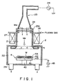
- the plasma processing apparatus has a vacuum vessel 2 made of aluminum or the like.
- the vacuum vessel 2 has a plasma chamber 21 in which plasma is produced and a processing chamber 22 located under the plasma chamber 21 and communicated with the plasma chamber 21.
- the vacuum vessel 2 is grounded to make electric potential zero.
- This vacuum vessel has an opening at the top thereof, and this opening is provided with a transmissive window 23 in an air-tight manner.
- the window 23 formed of a material which is transmissive to high frequency wave (microwave).
- the transmissive window 23 is made, for example, of aluminum nitride (A1N).
- A1N aluminum nitride
- the outside peripheral of the transmissive window 23 is supported by a support ring 23a in the air-tight manner.
- the transmissive window 23 and the support ring 23a maintain a vacuum condition inside the vacuum vessel 2.
- the top of the transmissive window 23 is provided with a wave guide 25 to supply microwave at a frequency of, for example, 2.45 GHz into the plasma chamber 21.
- the wave guide 25 can be configured by combining a rectangular wave guide, a cylindrical wave guide and a conical wave guide.
- the outlet end of the wave guide 25 is connected to the top of the transmissive window 23, and the inlet end of the wave guide 25 is connected to a high frequency electric source 24.
- the wave guide 25 guides microwave generated in the high frequency electric source 24 in TE mode, or converts the microwave guided in the TE mode to TM mode, to introduce the microwave into the plasma chamber through the transmissive window 23.
- Gas nozzles 26 are circumferentially arranged and equally spaced on the upper part of a side wall defining the plasma chamber 21.
- a plasma gas source (not shown) is connected to the gas nozzles 26.
- the gas nozzles 26 is capable of supplying plasma gas such as Ar gas and O 2 gas to the upper space of the plasma chamber 21 uniformly without irregularity. Further, although only two gas nozzles are shown on the drawing to avoid complexity, the actual number of the gas nozzles is more than that.
- a ring-shaped main electromagnetic coil 27 having a ring shape is arranged around the plasma chamber 21 close to the outside peripheral of the side wall defining the plasma chamber 21.
- a ring-shaped auxiliary electromagnetic coil (not shown) is also arranged on the lower part of the processing chamber 22. These coils can generate magnetic field Mf (for example magnetic field at 875 Gauss) over the plasma chamber 21 and the processing chamber 22 directed downward.
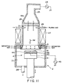
- a susceptor 4 for placing and holding thereon a wafer W is installed on a cylindrical support member 40 inside the processing chamber 22.
- the susceptor 4 comprises a dielectrics plate 42, in which a heater 43 and an electrode 44 is built, placed on a susceptor body 41.
- the loading surface of the susceptor 4 is configured as an electrostatic chuck:.
- a DC electric source for the electrostatic chuck (not shown) is connected to the electrode 44, to which a high frequency electric source 45 for applying bias voltage to introduce ion into the wafer W is also connected.
- exhaust pipes 28 are connected to the bottom of the processing chamber 22.
- the susceptor 4 used is of a fixed type without elevating function.
- a substrate to be processed, namely the wafer W, can be placed on the susceptor 4 by a carrying arm with an elevation function (not shown).
- the susceptor can be configured so as to be capable of elevating between a processing position and a loading/unloading position.
- the support member 40 is configured so as to penetrate through the bottom wall of the vacuum vessel 2 and to be capable of elevating while keeping air-tightness inside the vacuum vessel 2 (See embodiments shown in Fig. 11 and Fig. 20 to be described later).
- the upper part of the processing chamber 22, namely the portion connected to the plasma chamber 21, is provided with a process gas supply portion 5 having a hollow ring shape for introducing the process gas into the processing chamber 22.
- the internal space of the process gas supply portion 5 is divided, with respect to the radial direction of the ring, into two sections by a buffer plate 51.
- the buffer plate 51 is provided with gas holes 51a as shown in Fig. 2, and therefore a buffer chamber 52 and a gas chamber 53 are formed at the external side and internal side respectively in the process gas supply portion 5.
- Process gas supply pipes 54 (54a and 54b) are connected to the buffer chamber 52.
- the process gas (in this example, the process gas is a deposition gas for forming film) can be supplied from the process gas source to the buffer chamber 52 through these process gas supply pipes 54a and 54b.
- the buffer chamber 52 and the gas chamber 53 extending circumferentially plays a role of a process gas passage for allowing the process gas supplied through the process gas supply pipes to circumferentially flow in the process gas supply portion 5.
- the process gas supply portion 5 has an inside peripheral surface 50 inclining so as to gradually flare as it goes downward.
- the inside peripheral surface 50 is a part of a conical surface of a cone.
- the cone has a bottom plane including the surface to be processed of the wafer W placed on the susceptor 4, and an apex on the normal line at the center C of the wafer W to be processed. Note that "the normal line at the center of the surface of the substrate to be processed" is also referred to as "the central axis of the wafer.”
- a plurality of (in this embodiment, six) gas supply holes 55 is formed at the inside peripheral surface 50 equi-spaced around a circumference of the surface 50.
- the gas supply holes 55 in other words, the process gas introducing holes, are provided so that an axis A of each gas supply holes 55 shown by a dashed line in Fig. 2 diagonally crosses the surface of the wafer W to be processed placed on the susceptor 4 at an angle ⁇ , and axes A cross at the position the distance L apart from the wafer W upward (toward the gas supply hole 55) on the central axis of the wafer W shown by a chain line in Fig. 2.
- the axes A of the gas supply holes 55 crosses the wafer at the position P beyond the center C of the surface to be processed of the wafer W when viewed from the gas supply hole 55.
- axes A do not cross each other on the wafer W.
- each gas supply hole 55 crosses the surface to be processed of the wafer W, however, the axis A of each gas supply hole 55 may cross the plane including the surface to be processed of the wafer W at an external position of the surface to be processed of the wafer W in the manner described above.
- Combination of the angle ⁇ at which the axis A of the gas supply hole 55 crosses the surface of the wafer W to be processed and the distance L from the surface of the wafer W to be processed to the point at which each axis crosses each other is preferably 15 deg. ⁇ ⁇ ⁇ 65 deg. and 5 mm ⁇ L ⁇ 15 mm respectively, and more preferably 30 deg. ⁇ ⁇ ⁇ 45 deg. and 5 mm ⁇ L ⁇ 10 mm respectively (See embodiments to be described later).
- the inclination of the inside peripheral surface 50 in the process gas supply portion 5 and the position of the gas supply holes 55 are set to meet this condition.
- each gas supply hole 55 is configured so as to enlarge at an angle ⁇ as it goes from the position almost in the middle of a wall thickness D of the inside peripheral surface 50 to the outlet end (toward the center of the processing chamber 22), and also to enlarge as It goes from the position almost in the middle of a wall thickness D of the inside peripheral surface 50 to the inlet end.
- each gas supply hole 55 has a shape created by combining the two truncated cones.
- the thickness D is approximately 4 mm, and an inner diameter of the gas supply hole 55 almost at the middle of the thickness D is 2 mm.
- the angle ⁇ is preferably set at 30 to 150 deg. The actual angle can be selected from the values within this range according to dispersion characteristic of the process gas ejected through the gas supply holes 55.
- a shape of the gas supply hole 55 can be configure as a cylindrical one so that the inner diameter of the portion from the position almost in the middle of a wall thickness D of the inside peripheral surface 50 to the inlet end is constant as shown in Fig. 5 instead of the shape shown in Fig. 4.
- the shape of the outlet side of the gas supply hole 55 is similarly configured as that shown in Fig. 4.
- the buffer plate 51 is arranged in parallel with the inside peripheral surface 50 and the buffer chamber 52 is provided outside the gas chamber 53.
- an internal space of the process gas supply portion 5 can be horizontally divided into two sections by the buffer plate 51 to form the buffer chamber 52 at the upper portion and the gas chamber 53 at the lower portion respectively.
- inter-level isolation film consisting of, for example, fluorine added carbon film (hereafter referred to as "CF film")
- CF film fluorine added carbon film
- a gate valve (not shown) installed on the side wall of the vacuum vessel 2 is opened.
- the wafer W of, for example, 8 inch size on which surface aluminum wiring is formed is carried from a load lock chamber (not shown) into the vacuum vessel 2 by the carrying arm (not shown) and placed on the susceptor 4.
- High frequency wave (microwave) Mw at 2.45 GHz from the high frequency electric source 24 reaches a ceiling part of the vacuum vessel 2, and is introduced into the plasma chamber 21 through the transmissive window 23.
- magnet field Mf is formed in the vacuum vessel 2 by the main electromagnetic coil 27 and the auxiliary electromagnetic coil (not shown).
- electron cyclotron resonance is generated by an interaction between the magnetic field Mf and the microwave Mw.
- the electron cyclotron resonance ionizes the plasma gas to convert the gas into a plasma state having high density. Application of the plasma gas contributes to stabilize the plasma.
- the produced plasma flows from the plasma chamber 21 into the processing chamber 22 as a plasma flow.
- the C 4 F 8 gas and C 2 H 4 gas supplied to the processing chamber 22 is activated (the gas is converted into a plasma state) to form active species (plasma).
- plasma ion is introduced into the wafer W by the bias voltage, and cuts off an edge of the CF film accumulated on a pattern (concave part) of the surface of the wafer W by a spatter etching action of plasma ion to increase width.
- the plasma of the deposition gas forms the CF film to make it embedded in the concave. In this manner, the inter-level isolation film consisting of the CF film is formed.
- each gas supply hole 55 is formed so that its inner diameter enlarges toward the outlet side, the deposition gas can easily disperse not only in the direction of the axis A of the gas supply hole 55 but three-dimensionally from the axis A as a center. That is to say, the deposition gas disperses with directivity of expanding while inflating, namely with wide directivity. Since the axis A diagonally crosses the wafer W at an angle of ⁇ , the deposition gas diagonally blows out downward through each gas supply hole 55 with the aforementioned directivity as shown in Fig. 7.
- the deposition gas blowing out through each gas supply hole 55 is supplied so as to reach the position P on the surface of the wafer W while crossing at the position where the axis A crosses each other (See Fig. 2).
- the C 4 F 3 gas and C 2 H 4 gas are dispersed by the buffer plate 51 at the time of flowing from the buffer chamber 52 to the gas chamber 53, and further dispersed at the time of flowing from the gas chamber 53 the processing chamber 22 through the gas supply holes 55. Therefore, in comparison with the configuration without the buffer chamber 52, these several types of the deposition gas are supplied to the processing chamber 22 in a sufficiently mixed condition.
- the deposition gas disperses while expanding three-dimensionally from the axis of the gas supply holes 55 as the center, the deposition gas disperses in the embodiment shown in Fig. 8. Therefore, in comparison with the case of directivity of the deposition gas extending in a beam shape, namely the case of dispersion with narrow directivity (See Fig. 24 and Fig. 25), the deposition gas disperses in a wider zone. Therefore the concentration distribution of the deposition gas is equalized because the deposition gas can also spread to the peripheral part of the wafer easily. This results in an improvement of uniformity of thickness and in-plane property of the CF film to be formed.
- each gas supply hole 55 does not cross each other on the surface of the wafer, a singular point at which the deposition gas concentrates on the surface of the wafer is not produced. Therefore it does not happen that film thickness on a particular place of the wafer W becomes extremely larger than that on the other place. That is to say, since the axis A of each gas supply hole 55 crosses each other at the position the distance L higher than the wafer W on the central axis B of the wafer W, the deposition gas blowing out through each gas supply hole 55 does not concentrate on the reaching point Pe on the surface of the wafer W, and an area where gas blowing out through each gas supply hole 55 overlaps becomes comparatively large because of the directivity of gas spreading while expanding.
- the point on the wafer W directly under this overlapping area has no possibility to become the singular point of the CF film thickness. Since the point on the wafer W corresponding to the overlapping area of the deposition gas never becomes the singular point of the film thickness like this, this is also an advantage to improve the uniformity of the CF film thickness.
- the distance L is smaller than 5 mm or larger than 15 mm, the film thickness is affected even the overlapping area of the deposition gas is located above the wafer W by tests to be described later, it is preferable to set the distance L from 5 mm or more to 15 mm or less.
- the CF film thickness becomes thin at the central area because the gas supply rate at the center of the wafer W becomes low, and, as a result, the in-plane uniformity of the film thickness becomes worse.
- Vacuum processing apparatus shown in Figs. 1, 2 and 4 was used. A test to produce CF film on the wafer W of 8-inch size was performed. At this time, Ar gas was introduced to the plasma chamber 21 at the specified flow rate, and the C 4 F 8 gas and C 2 H 4 gas were introduced to the processing chamber 22 at the specified flow rate. High frequency power was set at 2500 W, bias power at 1500 W, and pressure inside the vacuum vessel at 0.2 Pa.
- the angle ⁇ of the gas supply holes 55 of the process gas supply portion 5 was changed in the range of 10 to 80 deg. and the distance L was changed in the range of 0 to 20 mm to prepare a plurality of samples. And film thickness distribution of the obtained samples was measured by an Opti-probe to investigate film profile.
- Table 1 shows evaluation results of the uniformity of the film thickness for each condition.
- the in-plane uniformity was evaluated by calculating mean values and standard deviations ⁇ of the film thickness at a plurality of measuring points (49 points this time) set so that the points are equally spaced on the surface of the wafer to be processed and by taking "3 ⁇ /mean value (%)" as an index representing the uniformity in the processed surface.
- the area 3 mm inward from the peripheral of the wafer W was excluded from the location of the measuring points.
- the axis A of each gas supply hole 55 inclines at an angle of ⁇ from the straight line connecting the gas supply hole 55 and the center of the wafer W in order to avoid passing through the central axis B of the wafer W viewed from the direction of the central axis B of the wafer W.
- the axes A of respective gas supply holes 55 crosses the wafer at the position P' locating far side of the center of the surface of the wafer W to be processed viewed from the gas supply hole 55.
- the deposition gas concentration does not become high or low at the particular location. Therefore the uniformity of the CF film thickness can be improved.
- the gas supply holes are provided in the external side of a plasma emission zone Pz.
- the plasma emission zone Pz meaning a zone in the processing chamber 22 into which the plasma generated in the plasma chamber 21 flows as plasma flow and a zone of which light emission is recognized from outside, is formed in a space over the susceptor 4 extending from the plasma chamber 21 to the processing chamber 22 as shown by the mark Pz in Fig. 10.
- the process gas supply portion 5 is configured similarly to the process gas supply portion 5 in the above-mentioned first embodiment, and the gas supply holes 55 are formed in the inside peripheral surface 50 of the process gas supply portion 5.
- the inside peripheral surface 50 is located at the position apart from the plasma emission zone Pz. Therefore the gas supply holes 55 are provided in the inside peripheral surface 50 and in the exterior of the plasma emission zone Pz.
- This configuration enables to prevent the gas supply holes 55 from being exposed to the plasma. Therefore adhesion of the process gas on the gas supply holes 55 can be avoided, and a throughput of the whole film processing can be improved when the film processing is performed.
- the gas supply holes 55 are provided inside the plasma emission zone Pz, the deposition gas collides with the plasma just after blowing out through the gas supply holes 55 during the deposition gas supply. Therefore a large amount of film deposits around the gas supply holes 55.
- the large amount of deposition causes peeling of film which becomes particles, and it takes long time to remove the large amount of deposition to prevent particle generation. Therefore, the throughput of the whole film processing decreases.
- the deposition gas blowing out through the gas supply holes 55 begins to disperse and collides with the plasma at the area apart from the gas supply holes 61. Therefore the film deposition around the gas supply holes 55 can be avoided. Then since an amount of the film deposition around the gas supply holes 55 considerably decreases, total cleaning time is reduced and the productivity of the whole deposition processing is improved.
- Fig. 11 through Fig. 16 Difference of the embodiment illustrated in Fig. 11 through Fig. 14 from the embodiment illustrated in Fig. 1 through Fig. 8 is that two types of the process gas are supplied to the processing chamber without mixed inside the ring-shaped process gas supply portion.
- an outline of the process gas supply portion 6 is identical to that of the process gas supply portion 5 shown in Fig. 2.
- the interior of the hollow ring-shaped process gas supply portion 6 is horizontally divided by a partition wall 6A to form two gas chambers. These two gas chambers play a role of process gas passages in the process gas supply portion 6.
- the space above the partition wall 6A is a first gas chamber 61, and the space below the wall a second gas chamber 62.
- a plurality of first gas supply holes 61a and a plurality of second gas supply holes 62a are formed and are circumferentially arranged with approximately constant interval.
- the first gas supply holes 61a and the second gas supply holes 62a are provided at eight points circumferentially and equally spaced.
- the first gas supply holes 61a are located inside the pitch circle of the second gas supply holes 62a. The axis of each gas supply hole 61a and 62a diagonally direct downward.
- a diameter L1 of the upper end of the inside peripheral surface 60 of the process gas supply portion 6 is set at 300 mm, an inclining angle ⁇ of the inside peripheral surface 60 of the process gas supply portion 6 at 45 deg., and a vertical distance L2 between the first gas supply holes 61a and the second gas supply holes 62a at 15 mm.
- the first gas supply holes 61a are formed at the position 15 mm downward from the upper end of the deposition gas supply portion 6.
- the first gas supply holes 61a is located at the position about 15 mm inward from the pitch circle of the second gas supply holes 62a. Accordingly the first gas supply holes 61a are located at the position 7.5 mm inward in comparison with conventional gas supply holes and the second gas supply holes 62a are located at the position 7.5 mm outward in comparison with conventional gas supply holes.
- gas supply holes 63 and 64 providing a plurality of, for example, two gas introduction passages almost equally spaced circumferentially are connected to the position each corresponding to the gas chamber 61 and 62 of the outer circumferential surface of the process gas supply portion 6.
- the other ends of these gas supply pipes 63 and 64 are connected to a gas supply source (not shown).
- the deposition processing is performed using two types of the deposition gas, namely the C 4 F 8 gas and the C 2 H 4 gas.
- the C 4 F 8 gas and the C 2 H 4 gas are simultaneously introduced to the deposition gas supply portion 6 through the supply pipe 63 and 64 respectively.
- the C 4 F 8 gas having relatively large specific gravity among the types of the deposition gas is introduced to the upper gas chamber 61 through the gas supply pipe 63.
- the C 2 H 4 gas having relatively small specific gravity among the types of the deposition gas is introduced to the lower gas chamber 62 through the gas supply pipe 64.
- Fig. 13 shows blow-out distribution of the C 4 F 8 gas and the C 2 H 4 gas with solid lines and dashed lines respectively.
- the C 2 H 4 gas having relatively small specific gravity disperses more easily in the radial direction of the wafer W rather than in the three-dimensionally expanding direction taking the axis of the gas supply hole as a center, and blows out showing beam-shaped blow-out distribution that extends slenderly and diagonally downward.
- the C 4 F 8 gas having relatively large specific gravity disperses more easily in the three-dimensionally expanding direction taking the axis of the gas supply hole as a center rather than in the radial direction of the wafer W, and blows out with the blow-out distribution having a shape that expands more widely than the C 2 H 4 gas.
- Fig. 14 illustrates the C 2 H 4 gas concentration distribution over the wafer with solid lines. The C 2 H 4 gas shows almost uniform concentration distribution over the wafer.
- the C 4 F 8 gas blows out through the position nearer toward the axis of the process gas supply portion than the conventional gas supply holes. Therefore, the distance between the gas supply holes 61a and the central axis of the ring-shaped process gas supply portion 6 decreases. And since the first gas supply holes 61a are located higher than the second gas supply holes 62a, it takes longer time for the deposition gas to come down to the wafer surface. Therefore, even if the blow-out distribution has a swelling shape, the top end of the deposition gas reaches the central part of the wafer when the end comes down to the wafer height, and the deposition gas spread all over the wafer.
- Fig. 14 illustrates the C 4 F 3 gas concentration distribution over the wafer with dashed lines. The C 4 F 8 gas shows almost uniform concentration distribution over the wafer.
- the concentration distribution of the C 4 F 8 gas and C 2 H 4 gas obtained from the process gas supply portion above the wafer of this embodiment shows better uniformity than that obtained not from the embodiment.
- a process gas supply portion 15 of the type that the C 4 F 8 gas and C 2 H 4 gas are supplied to a processing chamber 12 through the same gas supply holes as shown in Fig. 15 is used, the concentration distribution of each gas over the wafer becomes uneven due to the difference of the directivity of each gas (See Fig. 16).
- blow-out distribution directivity
- two types of deposition gas having different specific gravity can be supplied in almost uniform concentration distribution of each deposition gas over the wafer even if they are simultaneously supplied from the deposition gas supply portion 6 to the processing chamber 22.
- the deposition gas supplied over the wafer W is converted into plasma state by the plasma to become the active species, amounts of the active species of carbon and fluorine generated by the plasma becomes almost uniform in the wafer plane because the concentration distribution of each deposition gas are made uniform.
- the in-plane uniformity of the CF film property can be improved because the concentration distribution of carbon and fluorine in the CF film deposited on the wafer becomes almost uniform in the plane.
- the deposition gas supply portion can be configured by pipes instead of the ring-shaped deposition gas supply portion used in the embodiment shown in Fig. 12. That is to say, the gas supply pipes for the C 4 F 8 gas supply and the C 2 H 4 gas supply can be provided along the peripheral of the wafer. In this case, the outlets of the gas supply pipes for the C4F8 gas supply and the C 2 H 4 gas supply, namely the gas supply holes, may be arranged in the same geometrical manner as the gas supply holes 61a and 61b shown in Fig. 12.
- the plasma processing apparatus used in this test are configured so that: the diameter L1 of the end of the inside peripheral surface of the deposition gas supply portion 6 is 300 mm; the inclining angle ⁇ of the inside peripheral surface 60 of the deposition gas supply portion 6 is 45 deg.; the vertical distance L2 between the first gas supply hole 61a and the second gas supply hole 62a is 15 mm; the first gas supply hole 61a is provided 15 mm below the upper end of the deposition gas supply portion 6; and the second gas supply hole 61a is located at the position about 15 mm nearer to the central axis than the gas supply hole 62a.
- the objects of this embodiment are to improve a method for introducing gas to the ring-shaped gas supply portion and to make a blow-out rate through each gas supply hole to be provided in the process gas supply portion constant.
- a plurality of gas supply pipes for example four gas supply pipes 56, namely gas introducing passages, are connected to the position circumferentially arranged and almost equally spaced in the outside peripheral surface of the process gas supply portion 5 in this embodiment.
- each gas supply pipe is equipped with a mass flow controller 57 (57a through 57d).
- a ring-shaped gas chamber namely a process gas passage, is provided inside the process gas supply portion 5.
- Gas supply holes 53 namely gas introducing passages, are formed, for example, at 16 positions circumferentially arranged and almost equally spaced in its inside peripheral surface.
- Fig. 17 shows the gas supply pipes 56 in case that a type of deposition gas is supplied to the processing chamber 22, the gas supply pipes 56 for the other type of process gas corresponding to the types of the process gas to be supplied to the processing chamber 22 may be provided.
- each gas supply pipe is equipped with the mass flow controller.
- all types of the deposition gas are supplied to the processing chamber 22 through the process gas supply portion 5.
- the deposition gas is supplied to the process gas supply portion 5 in a condition that its flow rate is controlled by the mass flow controller 52, flows while dispersing in the process gas supply portion 5, and blows out to the processing chamber 22 through each gas supply hole 53 at an almost uniform flow rate.
- each gas supply pipe 56 is equipped with the mass flow controller 57, if the deposition gas is supplied, for example, at a flow rate of 100 sccm, and when the flow rate of the deposition gas is controlled at 25 sccm by each mass flow controller, the deposition gas flows through each gas supply pipe at the controlled flow rate, and is supplied through four positions circumferentially arranged and equally spaced in the outside peripheral surface at a flow rate of 25 sccm per position.
- each gas supply pipe 56 since the flow rate of the deposition gas at the downstream side of the mass flow controller 57 of each gas supply pipe 56 is controlled at a constant value even if gas line length of each gas supply pipe 56 is different from each other, the deposition gas is supplied to the deposition gas supply portion 5 through each gas supply pipe 56 at the same flow rate. Therefore in comparison with the case that the flow rate of the deposition gas supplied through each gas supply hole varies depending on the gas line length like the case (see Fig. 26) that the gas supply pipe is branched off to two pipes at the downstream side of the mass flow controller in the conventional plasma processing apparatus, the uniformity of the blow-out distribution of the deposition gas through the gas supply holes 53 can be improved.
- the deposition gas is supplied to the deposition gas supply portion 5 at the same flow rate through a number of positions equally spaced in the circumferential direction. Therefore deposition gas pressure in the deposition gas supply portion 5 easily becomes uniform circumferentially, and the blow-out distribution of the deposition gas through gas supply holes 56 becomes more uniform.
- the uniformity of the blow-out distribution of the deposition gas through gas supply holes 56 can be improved. And such uniformity of the blow-out distribution of the deposition gas brings the effect that the plasma of the deposition gas generated by the plasma flow can easily become uniform directly above the wafer W, and also the in-plane uniformity the film thickness of the CF film to be generated on the wafer W can be improved.
- Fig. 18A through Fig. 18D Four types of plasma equipment having different configuration of the gas supply portion and the gas supply pipes 56 to be connected to that portion (see Fig. 18A through Fig. 18D) were prepared.
- the plasma equipment provided with gas supply means shown in Fig. 18A, Fig. 18B, Fig. 18C and Fig. 18D are referred to as equipment A, equipment B, equipment C and equipment D respectively.
- Configuration of the gas supply portion 5 of the equipment A and the equipment B are substantially identical to the gas supply portion 5 shown in Fig. 2.
- the geometrical relation between the axis of each gas supply hole of the gas supply portion and the wafer W is identical to that of the embodiment shown in Fig. 2. Further, the eight gas supply holes were provided.
- a pair of the gas supply pipes 58a and 58b connected to C 4 F 8 gas supply source and C 2 H 4 gas supply source (not shown) respectively are provided with the mass flow controller 57 respectively.
- Both of the gas supply pipes 58a and 58b join into one gas supply pipe 58c at the downstream side of the mass flow controller 57.
- the gas supply pipe 58c further branches off to two pipes 58d and 58e which are connected to the gas supply portion at opposite positions 180 deg. apart. This configuration is substantially identical to the conventional one.
- the gas supply pipe 58c is connected to the ring-shaped gas supply portion 5 at the opposite position 180 deg. apart without branching off at the downstream side of the mass flow controller 58.
- the mass flow controllers of which number (in this example four) is obtained by multiplying the number of the connecting points of the gas supply pipes and the ring-shaped gas supply portions (in this example two) by the number of the types of process gas to be used (In this example two) are provided.
- the gas supply portion of the equipment D is formed based on the embodiment shown in Fig. 12. That is to say, two gas chambers (not shown in Fig. 18D) is formed inside the gas supply portion 5, and the upper gas chamber and the lower gas chamber are used to supply the C 4 F 3 gas and the C 2 H 4 gas respectively.
- a pair of gas supply pipes 58f and 58f exclusively used for the C 4 F 8 gas are connected to the ring-shaped gas supply portion at the opposite position 180 deg apart
- a pair of gas supply pipes 58g and 58g exclusively used for the C 2 H 4 gas are connected to the ring-shaped gas supply portion at the opposite position 180 deg apart.
- Connecting position of the gas supply pipe 58f exclusively used for the C 4 F 8 gas in the gas supply portion 5 is displaced by 90 deg from the connecting position of the gas supply pipe 58g exclusively used for C 2 H 4 gas.
- Each of the gas supply pipes 58f and 58g are equipped with the mass flow controller 57 respectively.
- the number of the gas supply holes provided in the inside peripheral surface of the gas supply portion 6 is eight and eight for the C 4 F 8 gas and the C 2 H 4 gas respectively, namely total 16.
- the Ar gas was supplied to the plasma chamber 21 at a flow rate of 150 sccm
- the C 4 F 8 gas and the C 2 H 4 gas were supplied from the deposition gas supply portion 5 or 6 to the processing chamber 22 at flow rates of 40 sccm and 30 sccm respectively
- the high frequency power from the high frequency power source 24 was set at 2700 W
- the bias power at 1500 W
- the deposition temperature at 400°C
- the CF film having the film thickness of 2 ⁇ m was deposited on the wafer in the same process condition as that of the above-mentioned embodiment.
- the uniformity of the film thickness of the equipment having the gas supply means based on this embodiment is improved in comparison with that of the equipment A having the conventional configuration. In other words, it was ensured that, when each gas supply pipe is equipped with the mass flow controller, the blow-out distribution from the deposition gas supply portion becomes uniform, and the uniformity of the CF film thickness is improved.
- Main object of the following embodiment is to improve thermal stability of the CF film, and the main feature is to supply a part of the deposition gas to the plasma chamber.
- a part of a plurality of gas nozzles 26 is assigned for plasma gas supply and the remaining for the deposition gas supply.
- the deposition gas source or the plasma gas source (not shown) is connected to each gas nozzle 26 according to its application.
- the gas nozzle 26 can supply a part of or all the plasma gas such as the Ar gas and O 2 gas and the deposition gas such as C n F m gas, for example C 4 F 8 gas, and C k H s gas, for example C 2 H 4 gas to the upper part inside the plasma chamber 21 uniformly without unevenness.
- the configuration of the other parts is identical to the plasma processing apparatus shown in Fig. 1 and Fig. 11.
- the plasma gas for example, Ar gas is introduced at a flow rate of 150 sccm and the C n f m , gas, for example, the C 4 F 8 gas among the deposition gas is introduced at a flow rate of 40 sccm both through the gas nozzles 26 to the plasma chamber 21.
- the C k H s gas for example, the C 2 H 4 gas is introduced from the process gas supply portion 5 to the processing chamber 22 at a flow rate of 30 sccm.
- the introduced gas flows downward inside the plasma chamber 21 by an exhaust action of the exhaust pipe 28.
- a process pressure in the vacuum vessel 2 is maintained at, for example, 016 Pa
- the bias voltage at 13.56 MHz and 1500 W is applied to the susceptor 4 by the high frequency power source portion 45, and the surface temperature of the susceptor 4 is set at 400°C.
- the high frequency (microwave) Mw at 2.45 GHz and 2700 W is introduced from the high frequency power source portion 24 to the plasma chamber 21 through the wave guide 25 and the transmission window 23, and the magnet field Mf directing downward at, for example, 875 Gauss is applied to the plasma chamber 21 by the electromagnetic coil 27 and the auxiliary electromagnetic coil.
- E (electric field) x H magnetic field Mf
- the plasma is generated, and the plasma density becomes maximum at the ECR point Pe. This resonance results in the conversion from Ar gas to a plasma and the increase of the plasma density.
- the generated plasma flows from the plasma chamber 21 into the processing chamber 22 as the plasma flow.
- the C 4 F 8 gas flows downward from the upper side of the ECR point Pe passing through the plasma.
- the C 4 F 8 gas is activated (converted into plasma state) by this plasma during passing through the plasma to form the active species (plasma).
- the C 2 H 4 gas forms the activated species by the plasma flow that flows into the processing chamber 22.
- the plasma ion in this example, Ar ion
- the bias voltage is pulled into the wafer W by the bias voltage, and cuts off an edge of the pattern (concave part) on the surface of the wafer W to increase width
- the CF film is deposited by the plasma of the deposition gas and embedded in the concave part along with the spatter etching action to form the inter-level isolation film consisting of the CF film.
- the C 4 F 8 gas introduced from the upper side of the ECR point Pe where the C 4 F 8 gas is generated passes the ECR point Pe while flowing toward the wafer W with the plasma by the time when the deposition gas reaches the surface of the wafer W. Therefore the C 4 F 8 gas passes the ECR point Pe where the plasma density is highest. And since the zone where the C 4 F 8 gas contacts with the plasma is wide because it extends from the zone where the plasma is generated to the zone directly above the wafer W, the C 4 F 8 gas contacts with the plasma for a long time. Therefore, the conversion of the C 4 F 8 gas into active species (plasma state) by the plasma is sufficiently promoted, and the thermal stability of the CF film deposited on the wafer W is improved.
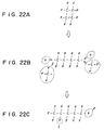
- the CF film actually deposited by the above-mentioned equipment was annealed for two hours at 425°C, and it was found that about 2% of fluorine is removed as gas. Thus it was confirmed that the thermal stability is higher than that of the conventional equipment.
- the creation of the network structure like this results in the decrease of the number of the activated species in the CF film, which becomes stronger than before. Therefore when the CF film is heated till a temperature higher than the deposition temperature, for example, till approximately 425°C, an amount of the fluorine separated from unstable species is small, and dissociated fluorine (fluorine surrounded by dashed lines in Fig. 21C) scarcely escapes from the network structure even if a part of the C-F bonding is dissociated by this heat. This is considered to improve the thermal stability of the CF film.
- this CF film is compared with that formed by the conventional plasma processing apparatus.
- all the deposition gas is introduced to the processing chamber, the plasma flow generated in the plasma chamber flows into the processing chamber and contacts with the deposition gas introduced here, and the deposition gas is converted into plasma state by this. Therefore, the C 4 F 8 gas cannot pass the ECR point Pe, and the zone where the gas contacts with the plasma is restricted to the zone above the wafer in the processing chamber. Consequently the time during which C 4 F 8 gas contacts with the plasma becomes considerably shorter than this embodiment.
- the C 4 F 8 gas is not sufficiently converted into plasma state, and this insufficiently converted C 4 F 8 gas is acquired by the CF film. If the dissociation of the C 4 F 8 molecule is small due to the insufficient conversion (to plasma state), for example in such a case that only one of the C-C bonding is dissociated even if the C 4 F 8 gas converted into plasma state (as shown In Fig. 22A), the C-C bonding is likely to be arranged as a linear chain (See Fig. 22B).
- the carbon or the fluorine is bonded with the carbon having non-bonding arm at the end.
- the number of the active species capable of bonding with the carbon at the end is small, the number of the non-bonding active species in the CF film increases. Therefore when the CF film is heated till high temperature, the fluorine easily escapes from the unstable species.
- the C-C bonding or the C-F bonding is cut off to generate solution or separation of the fluorine, the separated fluorine (fluorine surrounded by dashed lines in Fig. 22C) cannot easily confined within the CF film due to its linear chain one-layer structure. Therefore, it is considered that the fluorine escapes more easily than this embodiment, and the thermal stability is poor.
- the Ar gas, the C 4 F 8 gas and C 2 H 4 gas were supplied at flow rates of 150 sccm, 40 sccm and 30 sccm respectively, the high frequency power was set at 2700 W, and the bias power at 1500 W and the deposition temperature at 400°C to deposit the CF film having a thickness of 2 ⁇ m on the wafer in the similar process condition as the above-mentioned embodiment.
- the process gas was supplied to the plasma chamber 21 or the processing chamber 22 as shown in Table 2 below.
- the wafer provided with the CF film was once cooled down to room temperature, was subjected to heat treatment by keeping it in nitrogen atmosphere at 425°C for two hours, and cooled down to the room temperature in natural atmosphere.
- the thermal stability was compared based on a film reduction ratio before and after the heat treatment that is defined as [ ⁇ (CF film weight before heat treatment)-(CF film weight after heat treatment) ⁇ /(CF film weight before heat treatment)] x 100 .
- Example 1 and 2 when a part of the deposition gas is introduced to the plasma chamber (Example 1 and 2), the film reduction ratio becomes lower than that of Comparative example 1. Therefore it was confirmed that when a part of the deposition gas is introduced to the plasma chamber, an amount of escaped fluorine is small and the thermal stability is improved. In this case, when Example 1 and 2 are compared, the film reduction ratio of Example 1 is lower than that of Example 2. Therefore it was confirmed that it is preferable to introduce the C n F m gas, at least one of the deposition gas, to the plasma chamber 21. And when all the deposition gas is introduced to the plasma chamber 21 (Embodiment 3), the film reduction ratio becomes 1.8%. Therefore it was confirmed that it is more preferable to introduce all the deposition gas into the plasma chamber 21.
- the C n F m gas (n is an integer equal to or larger than 1, and m is an integer equal to or larger than 2) such as CF 4 gas, C 4 F 6 gas, C 4 F 8 gas, C 6 F 10 gas, C 6 F 6 gas and C 7 F 8 gas can be used
- the C k H s gas (k is an integer equal to or larger than 1, or equal to 0, and s is an integer equal to or larger than 2) such as H 2 gas, C 2 H 2 gas, C 2 H 4 gas and CH 4 gas can be used.
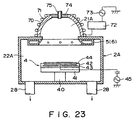
- plasma generation system is not limited to the ECR. That is to say, it may be induction bonding plasma processing apparatus as shown in Fig. 23.
- a plasma chamber 21B is divided by a semi-sphere-shaped dome 70.
- An induction coil 71 is wound along an external surface of the dome70.
- the induction coil 71 is connected to a high frequency power source 73 through a rectifier 72.
- An anode 74 can be installed on the top of the dome 70.
- the processing chamber side of the induction bonding plasma processing apparatus shown in Fig. 23 can be configured according to the ECR plasma processing apparatus described so far. Therefore in the induction bonding plasma processing apparatus shown in Fig. 23, configuration of the aforementioned ring-shaped process gas supply portion 5, 5A and 6 (Fig. 2 through Fig. 6, Fig. 9, Fig. 10 and Fig. 12) is applicable as a process gas supply portion. And configuration shown in Fig. 17 and Fig. 18 is applicable as a gas supply pipe arrangement.
- an introducing port 75 for supplying a part of the plasma gas can be installed on the top of the dome 70.
- an introducing port 75 for supplying a part of the process gas can be additionally installed on the top of the dome 70.
- the C n F m gas n is an integer equal to or larger than 1
- m is an integer equal to or larger than 2
- the plasma processing apparatus of this invention can be applied to a case of etching processing, for example, a case of etching silicon oxide film using CF type gas.
Abstract
Description
- The present invention relates to a plasma processing apparatus and a method for performing deposition process or etching process on a substrate to be processed, more specifically, to a device and a way for supplying process gas such as deposition gas and etching gas into a vacuum vessel.
- One of methods for applying deposition or etching treatment on a semi-conductor wafer is a process utilizing plasma. This process is performed by introducing a process gas into a vacuum vessel equipped with a wafer susceptor and, for example, by supplying electromagnetic energy to this process gas to produce a plasma. As electromagnetic energy supplying technique, a method utilizing electron cyclotron resonance (ECR) that is an interaction between microwave and magnetic field Mf, and a method called ICP (Inductive Coupled Plasma) in which a coil wound on a dome-shaped vessel gives electric field and the magnetic field Mf to the process gas are known.
- An example of conventional plasma processing apparatus utilizing the ECR is described by taking processing to form CF film (fluorine added carbon film) as an example based on Figure 24. Firstly, microwave at a frequency of 2.45 GHz is supplied into a plasma producing chamber 11 through a conductive wave tube (not shown), and high density plasma is produced from Ar gas (plasma gas) by simultaneously applying the magnetic field to the Ar gas using an electromagnetic coil (not shown) to utilize the interaction between the microwave and the magnetic field Mf. Active species is produced by activating deposition gas (C4F8 gas and C2H4 gas) introduced into a
deposition chamber 12, and a CF film is formed on a surface of the semiconductor wafer W (hereafter referred to as "Wafer W") placed on the susceptor 13. - At this time, the deposition gas is supplied through a deposition
gas supply portion 14. The depositiongas supply portion 14 is formed as a hollow ring shape, and its inside peripheral is provided with a plurality ofgas introducing holes 15 almost equally spaced circumferentially. Eachgas supply hole 15 is arranged so that it is nearly parallel to a surface of the wafer W to be processed and an outlet side of it faces the center of thedeposition chamber 12. Eachgas supply hole 15 has the same diameter from an inlet side through the outlet side. Figure 26 shows a conventional deposition gas supply system. In this gas supply system, the deposition gas is supplied from a gas supply source (not shown) through agas supply pipe 17. Thegas supply pipe 17 is equipped with amass flow controller 16 for adjusting a flow rate of the deposition gas. Thegas supply pipe 17 branches off to two ways at a downstream side of themass flow controller 16. And the gassupply pipe branches gas supply portion 14 at the positions 180 deg. apart from each other. Length of thegas supply pipes - Recently equipment capable of depositing uniform film on the wafer W has been required with the enlargement of wafer W diameter. It is important to introduce the deposition gas as uniformly as possible into a space above the surface of the wafer W to be processed in order to secure in-plane uniformity of the formed film. However, conventional plasma processing apparatus has the following problems:
- Firstly, since the inlet side through the outlet side of each
gas supply hole 15 are arranged on the circle having the same diameter, the deposition gas disperses as a beam slenderly elongating from thegas supply holes 15 horizontally, and does not three-dimensionally disperse taking an axis of thegas supply hole 15 as a center. Therefore, viewing from the direction perpendicular to the surface of the wafer W to be processed, distribution of the deposition gas becomes unequal as shown in Fig. 25. - Since flow resistance of the
gas supply pipes gas supply pipes gas supply pipes gas supply portion 14 are different from each other. Therefore, discharge rates of the deposition gas from each gas supply hole are different. - Furthermore, when different types of gas such as C4F8 gas and C2H4 gas are supplied, the C2H4 gas having relatively low specific gravity has directivity of narrow beam. On the other hand, the C4F8 gas having relatively high specific gravity easily disperses three-dimensionally taking the axis of the
gas supply hole 15 as the center. This difference of dispersion directivity results in unequal distribution of both gas above the surface of the wafer W to be processed. - For the above reasons, the conventional plasma processing apparatus does not provide sufficient uniformity of film thickness and film property in the processed surface. In addition, the etching process has also similar problem caused by unequal gas distribution above the surface to be processed.
- The object of the invention is to provide a plasma processing apparatus that can improve uniformity in the processed surface by improving uniformity of process gas distribution above the surface to be processed when performing the plasma processing by supplying process gas to a substrate through gas supply holes.
- In order to achieve the above object, the present invention provides the plasma processing apparatus which includes: a plasma chamber for producing plasma: a processing chamber connected to the plasma chamber and into which the plasma produced in the plasma chamber is introduced; a plasma gas introducing means for introducing the plasma gas into the plasma chamber, a susceptor arranged in the processing chamber to place a substrate to be processed; and a process gas introducing means for the processing chamber having a plurality of process gas introducing ports for supplying the process gas to the processing chamber, wherein each of the process gas introducing ports has an axis diagonally crossing a plane including a surface of the substrate to be processed placed on the susceptor at a specified crossing angle.
- A cross-sectional area of the process gas introducing port may be configured so that it increases as it approaches to an outlet end toward the processing chamber.
- The process gas introducing ports can be arranged so that axes of the respective introducing ports cross each other at a position, which is on a normal line at a center of a surface to be processed of the substrate placed on the susceptor, and the position is a specified distance apart from the surface to be processed toward the plasma chamber. In this case, an angle between the axes of the process gas introducing ports and a plane including the surface to be processed of the substrate is preferably 15 to 65 deg., and the distance from the surface to be processed to the position at which the axes of the respective process gas introducing ports cross each other is preferably 5 to 15 mm. More preferably, the angle that the axis of the process gas introducing port forms with the plane including the surface to be processed of the substrate is 30 to 45 deg., and the distance from the surface to be processed to the position where the axes of the process gas introducing ports cross each other is 5 to 10 mm.
- The axis of each of the process gas introducing port can be arranged so as not to cross the normal line at the center of the surface to be processed of the substrate placed on the susceptor.
- Furthermore, outlet ends of the process gas introducing ports can be located at the external part of a plasma emission zone.
- The process gas introducing means for the processing chamber can be formed as a hollow ring body having an inside peripheral surface, the body having a ring shape taking the normal line at the center of the surface to be processed of the substrate placed on the susceptor as a central axis. In this case, process gas passages for passing the process gas extending along the circumferential direction of the ring body is formed inside the ring body, and the process gas passages of the ring body are connected to the process gas introducing port and opens toward the inside peripheral surface.
- The plasma processing apparatus can be configured so as to be further includes a plurality of gas introducing passages connected, with intervals with respect to a circumferential direction of the process gas passage, to the process gas passage of the ring body; and a flow control device installed in each of the gas introducing passages.
- The plasma processing apparatus can be also configured so as to be further equipped with the process gas introducing means for the plasma chamber for supplying the process gas to the plasma chamber, and so as to convert the process gas supplied to the plasma chamber to an active species by the process gas introducing means for the plasma chamber. In this case, the process gas supplied to the plasma chamber by the process gas introducing means for the plasma chamber can be provided with the same composition as the process gas supplied to the processing chamber by the process gas introducing means for the processing chamber, and the process gas supplied to the plasma chamber by the process gas introducing means for the plasma chamber can be provided with the composition different from the process gas supplied to the processing chamber by the process gas introducing means for the processing chamber.
- When the plasma processing apparatus comprises a means for supplying microwave to the plasma chamber and a means for generating magnetic field in the plasma chamber, the apparatus can be configured so that the outlet end of each gas introducing port of the process gas introducing means for the plasma chamber is located at the position opposite to the processing chamber beyond the zone where electron cyclotron resonance condition within the plasma chamber is established.
- The gas introducing port of the process gas introducing means for the processing chamber can be configured so as to include a first gas introducing port, and a second gas introducing port that is located in the position lower than that of the first gas introducing port and is arranged so that the distance from the normal line at the center of the surface of the substrate to be processed to be placed on the susceptor to the outlet end of the second gas introducing port is larger than that from the normal line to the outlet end of the first gas introducing port. In this case, it is preferable to make the specific gravity of the process gas supplied through the first gas introducing port larger than that of the process gas supplied through the second gas introducing port.
- The process gas introducing means for the processing chamber can be formed as a hollow ring body having an inside peripheral surface, the body having a ring shape taking the normal line at the center of the surface to be processed of the substrate placed on the susceptor as a central axis. In this case, the means can be configured so that the first process gas passage and the second process gas passage circumferentially extending along the ring-shaped body are provided inside the ring-shaped body, the first and second process gas passages are independent from each other to prevent the gas flowing from one passage to the other, the first gas introducing port is connected to the first process gas passage and opens toward the inside peripheral surface of the ring-shaped body, and the second gas introducing port is connected to the second process gas passage and opens toward the inside peripheral surface of the ring-shaped body.
- According to the second aspect of the present invention, a plasma processing method including a process for placing the substrate to be processed on the susceptor arranged in the processing chamber, a process for supplying the process gas in the direction diagonally crossing the plane including the surface to be processed from a plurality of positions against the surface of the substrate to be processed and a process for producing plasma from the process gas to perform plasma processing on the substrate are provided.
- The processing to be performed on the substrate to be processed by the plasma processing apparatus may be either deposition processing or etching processing.
-
- Fig. 1 is a cross-sectional view illustrating an embodiment of plasma processing apparatus related to the present invention;
- Fig. 2 is an enlarged cross-sectional view illustrating a configuration of a gas supply portion and a geometrical arrangement relation between a substrate and a gas supply hole in the plasma processing apparatus shown in Fig. 1;
- Fig. 3 is a plan view illustrating the geometrical arrangement relation between the substrate and the gas supply hole shown in Fig. 2;
- Fig. 4 is an enlarged cross-sectional view showing a cross-sectional shape of the gas supply hole;
- Fig. 5 is an enlarged cross-sectional view showing the other embodiment of the gas supply hole;
- Fig. 6 is an enlarged cross-sectional view showing the other example of a structure of a buffer chamber in a process gas supply portion;
- Fig. 7 is a side cross-sectional view illustrating directivity of deposition gas ejected through the gas supply hole of the present invention;
- Fig. 8 is a diagrammatic plan view illustrating the directivity of the deposition gas ejected through the gas supply hole of the present invention and viewed from the Z direction shown in Fig. 7;
- Fig. 9 is a view illustrating the other embodiment having the gas supply holes in a different direction;
- Fig. 10 is a cross-sectional view of the main portion illustrating the other embodiment of the plasma processing apparatus wherein the relation between the process gas supply portion and plasma emission zone is specified;
- Fig. 11 is a cross-sectional view illustrating the other embodiment of the plasma processing apparatus wherein the construction of the process gas supply portion is changed;
- Fig. 12 is a cross-sectional view illustrating the construction of the process gas supply portion of the plasma processing apparatus shown in Fig. 11;
- Fig. 13 is a diagram illustrating an ejecting condition of the process gas when the process gas supply portion shown in Fig. 12 is used;
- Fig. 14 is a diagram illustrating concentration distribution of the process gas directly above a wafer when the process gas is ejected as shown in Fig. 13;
- Fig. 15 is a diagram illustrating the ejecting condition of the process gas when a plurality of types of the process gas is mixed in the process gas supply portion and ejected through a common gas supply hole (example for comparison);
- Fig. 16 is a diagram illustrating the concentration distribution of the process gas directly above the wafer when the process gas is ejected as shown in Fig. 15;
- Fig. 17 is a diagrammatic plan view illustrating the other embodiment of the plasma processing apparatus wherein a supply system for supplying the process gas to the process gas supply portion is changed;
- Figs. 18A, 18B, 18C and 18D are diagrammatic plan views illustrating the process gas supply system of the plasma processing apparatus used in a test;
- Fig. 19 is a chart illustrating test results by the plasma processing apparatus shown in Fig. 18A through Fig. 18D and uniformity of film thickness;
- Fig. 20 is a cross-sectional view illustrating the other embodiment of the plasma processing apparatus configured so that the process gas can be partially introduced to the plasma chamber;
- Figs. 21A, 21B and 21C are explanatory views illustrating the manner in which C4F8 gas is dissociated by the plasma when CF film is formed using the plasma processing apparatus shown in Fig. 20;
- Figs. 22A, 22B and 22C are explanatory views illustrating the manner in which C4F8 gas is dissociated by the plasma when CF film is formed using conventional plasma processing apparatus;
- Fig. 23 is a cross-sectional view showing an example where the invention applies to ICP type of plasma processing apparatus;
- Fig. 24 is a diagrammatic cross-sectional view illustrating conventional plasma processing apparatus;
- Fig. 25 is a diagrammatic plan view illustrating the directivity of the process gas ejected through the gas supply hole of the plasma processing apparatus shown in Fig. 24 and viewed from the Z direction shown in Fig. 24; and
- Fig. 26 is a diagrammatic plan view illustrating a construction of the process gas supply system of the conventional plasma processing apparatus.
-
- A preferred embodiment of plasma processing apparatus according to the present invention will be described referring to Fig. 1 through Fig. 7. As shown in Fig. 1, the plasma processing apparatus has a
vacuum vessel 2 made of aluminum or the like. Thevacuum vessel 2 has aplasma chamber 21 in which plasma is produced and aprocessing chamber 22 located under theplasma chamber 21 and communicated with theplasma chamber 21. Thevacuum vessel 2 is grounded to make electric potential zero. - This vacuum vessel has an opening at the top thereof, and this opening is provided with a
transmissive window 23 in an air-tight manner. Thewindow 23 formed of a material which is transmissive to high frequency wave (microwave). Thetransmissive window 23 is made, for example, of aluminum nitride (A1N). The outside peripheral of thetransmissive window 23 is supported by a support ring 23a in the air-tight manner. Thetransmissive window 23 and the support ring 23a maintain a vacuum condition inside thevacuum vessel 2. - The top of the
transmissive window 23 is provided with awave guide 25 to supply microwave at a frequency of, for example, 2.45 GHz into theplasma chamber 21. Thewave guide 25 can be configured by combining a rectangular wave guide, a cylindrical wave guide and a conical wave guide. The outlet end of thewave guide 25 is connected to the top of thetransmissive window 23, and the inlet end of thewave guide 25 is connected to a high frequencyelectric source 24. Thewave guide 25 guides microwave generated in the high frequencyelectric source 24 in TE mode, or converts the microwave guided in the TE mode to TM mode, to introduce the microwave into the plasma chamber through thetransmissive window 23. -
Gas nozzles 26 are circumferentially arranged and equally spaced on the upper part of a side wall defining theplasma chamber 21. A plasma gas source (not shown) is connected to thegas nozzles 26. The gas nozzles 26 is capable of supplying plasma gas such as Ar gas and O2 gas to the upper space of theplasma chamber 21 uniformly without irregularity. Further, although only two gas nozzles are shown on the drawing to avoid complexity, the actual number of the gas nozzles is more than that. - A ring-shaped main
electromagnetic coil 27 having a ring shape is arranged around theplasma chamber 21 close to the outside peripheral of the side wall defining theplasma chamber 21. A ring-shaped auxiliary electromagnetic coil (not shown) is also arranged on the lower part of theprocessing chamber 22. These coils can generate magnetic field Mf (for example magnetic field at 875 Gauss) over theplasma chamber 21 and theprocessing chamber 22 directed downward. - A
susceptor 4 for placing and holding thereon a wafer W is installed on acylindrical support member 40 inside theprocessing chamber 22. Thesusceptor 4 comprises adielectrics plate 42, in which aheater 43 and anelectrode 44 is built, placed on asusceptor body 41. The loading surface of thesusceptor 4 is configured as an electrostatic chuck:. A DC electric source for the electrostatic chuck (not shown) is connected to theelectrode 44, to which a high frequencyelectric source 45 for applying bias voltage to introduce ion into the wafer W is also connected. Further,exhaust pipes 28 are connected to the bottom of theprocessing chamber 22. Thesusceptor 4 used is of a fixed type without elevating function. A substrate to be processed, namely the wafer W, can be placed on thesusceptor 4 by a carrying arm with an elevation function (not shown). - In addition, the susceptor can be configured so as to be capable of elevating between a processing position and a loading/unloading position. In this case, the
support member 40 is configured so as to penetrate through the bottom wall of thevacuum vessel 2 and to be capable of elevating while keeping air-tightness inside the vacuum vessel 2 (See embodiments shown in Fig. 11 and Fig. 20 to be described later). - On the other hand, the upper part of the
processing chamber 22, namely the portion connected to theplasma chamber 21, is provided with a processgas supply portion 5 having a hollow ring shape for introducing the process gas into theprocessing chamber 22. The internal space of the processgas supply portion 5 is divided, with respect to the radial direction of the ring, into two sections by abuffer plate 51. Thebuffer plate 51 is provided with gas holes 51a as shown in Fig. 2, and therefore abuffer chamber 52 and agas chamber 53 are formed at the external side and internal side respectively in the processgas supply portion 5. Process gas supply pipes 54 (54a and 54b) are connected to thebuffer chamber 52. The process gas (in this example, the process gas is a deposition gas for forming film) can be supplied from the process gas source to thebuffer chamber 52 through these processgas supply pipes buffer chamber 52 and thegas chamber 53 extending circumferentially plays a role of a process gas passage for allowing the process gas supplied through the process gas supply pipes to circumferentially flow in the processgas supply portion 5. - The process
gas supply portion 5 has an insideperipheral surface 50 inclining so as to gradually flare as it goes downward. In this embodiment, the insideperipheral surface 50 is a part of a conical surface of a cone. The cone has a bottom plane including the surface to be processed of the wafer W placed on thesusceptor 4, and an apex on the normal line at the center C of the wafer W to be processed. Note that "the normal line at the center of the surface of the substrate to be processed" is also referred to as "the central axis of the wafer." - A plurality of (in this embodiment, six) gas supply holes 55 is formed at the inside
peripheral surface 50 equi-spaced around a circumference of thesurface 50. The gas supply holes 55, in other words, the process gas introducing holes, are provided so that an axis A of each gas supply holes 55 shown by a dashed line in Fig. 2 diagonally crosses the surface of the wafer W to be processed placed on thesusceptor 4 at an angle , and axes A cross at the position the distance L apart from the wafer W upward (toward the gas supply hole 55) on the central axis of the wafer W shown by a chain line in Fig. 2. - In the above arrangement, the axes A of the gas supply holes 55 crosses the wafer at the position P beyond the center C of the surface to be processed of the wafer W when viewed from the
gas supply hole 55. In addition, axes A do not cross each other on the wafer W. - In the embodiment shown in Fig. 2, the axis A of each gas supply holes 55 crosses the surface to be processed of the wafer W, however, the axis A of each
gas supply hole 55 may cross the plane including the surface to be processed of the wafer W at an external position of the surface to be processed of the wafer W in the manner described above. - Combination of the angle at which the axis A of the
gas supply hole 55 crosses the surface of the wafer W to be processed and the distance L from the surface of the wafer W to be processed to the point at which each axis crosses each other is preferably 15 deg. ≦ ≦ 65 deg. and 5 mm ≦L≦15 mm respectively, and more preferably 30 deg. ≦ ≦ 45 deg. and 5 mm ≦L≦10 mm respectively (See embodiments to be described later). The inclination of the insideperipheral surface 50 in the processgas supply portion 5 and the position of the gas supply holes 55 are set to meet this condition. - Especially as shown in Fig. 4 in detail, each
gas supply hole 55 is configured so as to enlarge at an angle α as it goes from the position almost in the middle of a wall thickness D of the insideperipheral surface 50 to the outlet end (toward the center of the processing chamber 22), and also to enlarge as It goes from the position almost in the middle of a wall thickness D of the insideperipheral surface 50 to the inlet end. In other words, eachgas supply hole 55 has a shape created by combining the two truncated cones. - In the embodiment shown in Fig. 4, the thickness D is approximately 4 mm, and an inner diameter of the
gas supply hole 55 almost at the middle of the thickness D is 2 mm. In addition, the angle α is preferably set at 30 to 150 deg. The actual angle can be selected from the values within this range according to dispersion characteristic of the process gas ejected through the gas supply holes 55. - A shape of the
gas supply hole 55 can be configure as a cylindrical one so that the inner diameter of the portion from the position almost in the middle of a wall thickness D of the insideperipheral surface 50 to the inlet end is constant as shown in Fig. 5 instead of the shape shown in Fig. 4. In this case also, the shape of the outlet side of thegas supply hole 55 is similarly configured as that shown in Fig. 4. - In the embodiment shown in Fig. 2, the
buffer plate 51 is arranged in parallel with the insideperipheral surface 50 and thebuffer chamber 52 is provided outside thegas chamber 53. Instead of this, an internal space of the processgas supply portion 5 can be horizontally divided into two sections by thebuffer plate 51 to form thebuffer chamber 52 at the upper portion and thegas chamber 53 at the lower portion respectively. - Then operation of the above-mentioned plasma processing apparatus is described taking the case of forming inter-level isolation film consisting of, for example, fluorine added carbon film (hereafter referred to as "CF film") on the wafer W, namely the substrate to be processed, as an example.
- Firstly, a gate valve (not shown) installed on the side wall of the
vacuum vessel 2 is opened. Next, the wafer W of, for example, 8 inch size on which surface aluminum wiring is formed is carried from a load lock chamber (not shown) into thevacuum vessel 2 by the carrying arm (not shown) and placed on thesusceptor 4. - Then the gate valve is tightly closed. Internal atmosphere is exhausted through an
exhaust pipe 28 to create a vacuum condition having the specified vacuum pressure. Then Ar gas (plasma gas) is introduced into theplasma chamber 21 through thegas nozzle 26 at the specified flow rate. Further, C4F8 gas and C2H4 gas are introduced as deposition gas into theprocessing chamber 22 from the processgas supply portion 5 at the specified flow rate respectively. And in a condition that a pressure inside thevacuum vessel 2 is maintained at the specified process pressure, bias voltage at 13.56 MHz is applied to thesusceptor 4 by a high frequencyelectric source 45, and a surface temperature of thesusceptor 4 is set, for example, at 400°C. - High frequency wave (microwave) Mw at 2.45 GHz from the high frequency
electric source 24 reaches a ceiling part of thevacuum vessel 2, and is introduced into theplasma chamber 21 through thetransmissive window 23. On the other hand, magnet field Mf is formed in thevacuum vessel 2 by the mainelectromagnetic coil 27 and the auxiliary electromagnetic coil (not shown). At the point where an intensity of the magnetic field Mf becomes 875 Gauss, electron cyclotron resonance is generated by an interaction between the magnetic field Mf and the microwave Mw. The electron cyclotron resonance ionizes the plasma gas to convert the gas into a plasma state having high density. Application of the plasma gas contributes to stabilize the plasma. - The produced plasma flows from the
plasma chamber 21 into theprocessing chamber 22 as a plasma flow. The C4F8 gas and C2H4 gas supplied to theprocessing chamber 22 is activated (the gas is converted into a plasma state) to form active species (plasma). On the other hand, plasma ion is introduced into the wafer W by the bias voltage, and cuts off an edge of the CF film accumulated on a pattern (concave part) of the surface of the wafer W by a spatter etching action of plasma ion to increase width. Along with this spatter etching action, the plasma of the deposition gas forms the CF film to make it embedded in the concave. In this manner, the inter-level isolation film consisting of the CF film is formed. - Now the manner of supply of the deposition gas supplied from the process
gas supply portion 5 to theprocessing chamber 22 is described in detail using Fig. 2. Firstly, the C4F8 gas and C2H4 gas supplied from the processgas supply pipes buffer chamber 52 disperse toward thegas chamber 53 through the gas hole 51a, and blow out through thegas supply hole 55 into theprocessing chamber 22. - At this time, since each
gas supply hole 55 is formed so that its inner diameter enlarges toward the outlet side, the deposition gas can easily disperse not only in the direction of the axis A of thegas supply hole 55 but three-dimensionally from the axis A as a center. That is to say, the deposition gas disperses with directivity of expanding while inflating, namely with wide directivity. Since the axis A diagonally crosses the wafer W at an angle of , the deposition gas diagonally blows out downward through eachgas supply hole 55 with the aforementioned directivity as shown in Fig. 7. Since the axes A of the respective gas supply holes 55 are configured so as to cross at the position the distance L upward from the wafer W on the central axis B of the wafer W, the deposition gas blowing out through eachgas supply hole 55 is supplied so as to reach the position P on the surface of the wafer W while crossing at the position where the axis A crosses each other (See Fig. 2). - When the deposition gas is supplied in this manner, the C4F3 gas and C2H4 gas are dispersed by the
buffer plate 51 at the time of flowing from thebuffer chamber 52 to thegas chamber 53, and further dispersed at the time of flowing from thegas chamber 53 theprocessing chamber 22 through the gas supply holes 55. Therefore, in comparison with the configuration without thebuffer chamber 52, these several types of the deposition gas are supplied to theprocessing chamber 22 in a sufficiently mixed condition. - Therefore, a phenomenon that occurs when these deposition gas is not sufficiently mixed, namely a phenomenon where the concentration of the C4F8 gas is high while that of the C2H4 gas low in a certain area and the concentration of the C4F8 gas is low while that of the C2H4 gas high in the other area, is generated less frequently. Since this results in a situation that concentration distribution of carbon and fluorine in the CF film formed on the wafer W becomes almost uniform in the surface, uniformity of CF film property can be improved. Since the C4F8 gas and C2H4 gas do not react only by mixing, this type of configuration is effective.
- Since the deposition gas disperses while expanding three-dimensionally from the axis of the gas supply holes 55 as the center, the deposition gas disperses in the embodiment shown in Fig. 8. Therefore, in comparison with the case of directivity of the deposition gas extending in a beam shape, namely the case of dispersion with narrow directivity (See Fig. 24 and Fig. 25), the deposition gas disperses in a wider zone. Therefore the concentration distribution of the deposition gas is equalized because the deposition gas can also spread to the peripheral part of the wafer easily. This results in an improvement of uniformity of thickness and in-plane property of the CF film to be formed.
- Furthermore, since the axis A of each
gas supply hole 55 does not cross each other on the surface of the wafer, a singular point at which the deposition gas concentrates on the surface of the wafer is not produced. Therefore it does not happen that film thickness on a particular place of the wafer W becomes extremely larger than that on the other place. That is to say, since the axis A of eachgas supply hole 55 crosses each other at the position the distance L higher than the wafer W on the central axis B of the wafer W, the deposition gas blowing out through eachgas supply hole 55 does not concentrate on the reaching point Pe on the surface of the wafer W, and an area where gas blowing out through eachgas supply hole 55 overlaps becomes comparatively large because of the directivity of gas spreading while expanding. Therefore, the point on the wafer W directly under this overlapping area has no possibility to become the singular point of the CF film thickness. Since the point on the wafer W corresponding to the overlapping area of the deposition gas never becomes the singular point of the film thickness like this, this is also an advantage to improve the uniformity of the CF film thickness. - Since we have recognized that, when the distance L is smaller than 5 mm or larger than 15 mm, the film thickness is affected even the overlapping area of the deposition gas is located above the wafer W by tests to be described later, it is preferable to set the distance L from 5 mm or more to 15 mm or less.
- By the way, it may be possible to avoid the deposition gas from overlapping with each other to improve the in-plane uniformity of the film thickness. This is achieved by allowing the axis A to cross the wafer surface at the point located near side of the center of the wafer W viewing from the
gas supply hole 55. However in this kind of configuration, the CF film thickness becomes thin at the central area because the gas supply rate at the center of the wafer W becomes low, and, as a result, the in-plane uniformity of the film thickness becomes worse. - Now, a test example performed actually by the inventors to confirm an advantage of the first embodiment is described. Vacuum processing apparatus shown in Figs. 1, 2 and 4 was used. A test to produce CF film on the wafer W of 8-inch size was performed. At this time, Ar gas was introduced to the
plasma chamber 21 at the specified flow rate, and the C4F8 gas and C2H4 gas were introduced to theprocessing chamber 22 at the specified flow rate. High frequency power was set at 2500 W, bias power at 1500 W, and pressure inside the vacuum vessel at 0.2 Pa. - The angle of the gas supply holes 55 of the process
gas supply portion 5 was changed in the range of 10 to 80 deg. and the distance L was changed in the range of 0 to 20 mm to prepare a plurality of samples. And film thickness distribution of the obtained samples was measured by an Opti-probe to investigate film profile. - As a result of this test, it was confirmed that the smaller the angle becomes, the larger the film thickness at the central part becomes than that of the peripheral part, and the larger the angle becomes, the smaller the film thickness at the central part becomes than that of the peripheral part. In addition, from the test performed by changing the distance L, it was confirmed that when L is smaller than 5 mm, an amount of deposition at the center increases, and when L is larger than 15 mm, an amount of deposition at the peripheral increases. The reason of this phenomenon is considered that when L is smaller than 5 mm, joining point of the deposition gas approaches too close to the wafer surface, the gas through each
gas supply hole 55 overlaps in the almost same condition as the case in which the axes A of respective gas supply holes 55 crosses each other on the wafer surface, and the singular point is easily generated at the central part. On the other hand, it is considered that, when L is larger than 15 mm, the distance between the center C of the wafer and the position P becomes too large, and void is easily generated at the central part. - Table 1 shows evaluation results of the uniformity of the film thickness for each condition. The in-plane uniformity was evaluated by calculating mean values and standard deviations σ of the film thickness at a plurality of measuring points (49 points this time) set so that the points are equally spaced on the surface of the wafer to be processed and by taking "3σ /mean value (%)" as an index representing the uniformity in the processed surface. In addition, the area 3 mm inward from the peripheral of the wafer W was excluded from the location of the measuring points.
Angle deg L=0 mm L=5 mm L=10 mm L=15 mm L=20 mm 10 10.3 8.3 9.1 8.1 11.3 15 9.8 4.8 5.3 5.7 10.2 30 9.1 4.6 4.1 5.5 9.3 45 8.5 4.5 4.2 6.2 8.2 60 8.9 4.2 5.1 6.3 7.9 63 9.6 5.0 5.2 6.9 8.1 65 10.4 5.8 5.4 7.1 8.5 70 12.5 9.2 5.8 7.3 9.1 80 30.1 22.0 10.0 10.5 12.1 - When Table 1 is viewed based on the above analysis results, it is understood that it is preferable to combine the angle of 15 deg.≦ ≦ 65 deg. and the distance L of 5 mm≦L≦15 mm and it is more preferable to combine the angle of 30 deg.≦ ≦ 45 deg. and the distance L of 5 mm≦L≦10 mm in order to improve the uniformity of the film thickness.
- Now, another other embodiment of the gas supply holes 55 is described referring to Fig. 9. In the embodiment shown in Fig. 9, the axis A of each
gas supply hole 55 inclines at an angle of δ from the straight line connecting thegas supply hole 55 and the center of the wafer W in order to avoid passing through the central axis B of the wafer W viewed from the direction of the central axis B of the wafer W. The axes A of respective gas supply holes 55 crosses the wafer at the position P' locating far side of the center of the surface of the wafer W to be processed viewed from thegas supply hole 55. - Since the axes A does not cross each other on the surface of the wafer W and the axes does not cross the wafer surface at the position locating near side of the center C even in this configuration, the deposition gas concentration does not become high or low at the particular location. Therefore the uniformity of the CF film thickness can be improved.
- Now, another embodiment of the present invention is described referring to Fig. 10. In this embodiment, the gas supply holes are provided in the external side of a plasma emission zone Pz. Here, the plasma emission zone Pz, meaning a zone in the
processing chamber 22 into which the plasma generated in theplasma chamber 21 flows as plasma flow and a zone of which light emission is recognized from outside, is formed in a space over thesusceptor 4 extending from theplasma chamber 21 to theprocessing chamber 22 as shown by the mark Pz in Fig. 10. - In this example, the process
gas supply portion 5 is configured similarly to the processgas supply portion 5 in the above-mentioned first embodiment, and the gas supply holes 55 are formed in the insideperipheral surface 50 of the processgas supply portion 5. However, in this example, the insideperipheral surface 50 is located at the position apart from the plasma emission zone Pz. Therefore the gas supply holes 55 are provided in the insideperipheral surface 50 and in the exterior of the plasma emission zone Pz. - This configuration enables to prevent the gas supply holes 55 from being exposed to the plasma. Therefore adhesion of the process gas on the gas supply holes 55 can be avoided, and a throughput of the whole film processing can be improved when the film processing is performed. In other words, if the gas supply holes 55 are provided inside the plasma emission zone Pz, the deposition gas collides with the plasma just after blowing out through the gas supply holes 55 during the deposition gas supply. Therefore a large amount of film deposits around the gas supply holes 55. The large amount of deposition causes peeling of film which becomes particles, and it takes long time to remove the large amount of deposition to prevent particle generation. Therefore, the throughput of the whole film processing decreases.
- However, when the gas supply holes 55 are provided outside the plasma emission zone Pz, the deposition gas blowing out through the gas supply holes 55 begins to disperse and collides with the plasma at the area apart from the gas supply holes 61. Therefore the film deposition around the gas supply holes 55 can be avoided. Then since an amount of the film deposition around the gas supply holes 55 considerably decreases, total cleaning time is reduced and the productivity of the whole deposition processing is improved.
- Now, another embodiment of the plasma processing apparatus of the present invention is described referring to Fig. 11 through Fig. 16. Difference of the embodiment illustrated in Fig. 11 through Fig. 14 from the embodiment illustrated in Fig. 1 through Fig. 8 is that two types of the process gas are supplied to the processing chamber without mixed inside the ring-shaped process gas supply portion. In addition, an outline of the process
gas supply portion 6 is identical to that of the processgas supply portion 5 shown in Fig. 2. - Especially as shown in Fig. 12 in detail, the interior of the hollow ring-shaped process
gas supply portion 6 is horizontally divided by a partition wall 6A to form two gas chambers. These two gas chambers play a role of process gas passages in the processgas supply portion 6. The space above the partition wall 6A is afirst gas chamber 61, and the space below the wall asecond gas chamber 62. - At the positions corresponding to the
first gas chamber 61 and thesecond gas chamber 62 of the insideperipheral surface 60, a plurality of firstgas supply holes 61a and a plurality of secondgas supply holes 62a are formed and are circumferentially arranged with approximately constant interval. In this example, the firstgas supply holes 61a and the secondgas supply holes 62a are provided at eight points circumferentially and equally spaced. The firstgas supply holes 61a are located inside the pitch circle of the secondgas supply holes 62a. The axis of eachgas supply hole - A diameter L1 of the upper end of the inside
peripheral surface 60 of the processgas supply portion 6 is set at 300 mm, an inclining angle β of the insideperipheral surface 60 of the processgas supply portion 6 at 45 deg., and a vertical distance L2 between the firstgas supply holes 61a and the secondgas supply holes 62a at 15 mm. The firstgas supply holes 61a are formed at theposition 15 mm downward from the upper end of the depositiongas supply portion 6. The firstgas supply holes 61a is located at the position about 15 mm inward from the pitch circle of the secondgas supply holes 62a. Accordingly the firstgas supply holes 61a are located at the position 7.5 mm inward in comparison with conventional gas supply holes and the secondgas supply holes 62a are located at the position 7.5 mm outward in comparison with conventional gas supply holes. - And ends of gas supply holes 63 and 64 providing a plurality of, for example, two gas introduction passages almost equally spaced circumferentially are connected to the position each corresponding to the
gas chamber gas supply portion 6. The other ends of thesegas supply pipes - In addition, although two gas chamber corresponding the case in which two types of the deposition gas are supplied to the
processing chamber 22 are shown in the drawing, more number of gas chambers can be provided in the processgas supply portion 6 corresponding to the number of types of the process gas. - Now the case that the deposition processing is performed using two types of the deposition gas, namely the C4F8 gas and the C2H4 gas, is considered. The C4F8 gas and the C2H4 gas are simultaneously introduced to the deposition
gas supply portion 6 through thesupply pipe upper gas chamber 61 through thegas supply pipe 63. The C2H4 gas having relatively small specific gravity among the types of the deposition gas is introduced to thelower gas chamber 62 through thegas supply pipe 64. The C4F8 gas and the C2H4 gas, circumferentially flowing in thegas chamber gas supply holes 61a and the secondgas supply holes 62a toward the zone radially inside the depositiongas supply portion 6, and further toward the wafer F almost equally in the circumferential direction and diagonally downward. - Fig. 13 shows blow-out distribution of the C4F8 gas and the C2H4 gas with solid lines and dashed lines respectively. The C2H4 gas having relatively small specific gravity disperses more easily in the radial direction of the wafer W rather than in the three-dimensionally expanding direction taking the axis of the gas supply hole as a center, and blows out showing beam-shaped blow-out distribution that extends slenderly and diagonally downward. On the other hand, the C4F8 gas having relatively large specific gravity disperses more easily in the three-dimensionally expanding direction taking the axis of the gas supply hole as a center rather than in the radial direction of the wafer W, and blows out with the blow-out distribution having a shape that expands more widely than the C2H4 gas.
- Mere, since the C2H4 gas blows out through the position farther from the axis of the process gas supply portion than the conventional gas supply holes, the top end of each beam of the C2H4 gas blowing out through each of the second
gas supply holes 62a does not overlap, or slightly overlaps each other, and the gas blows out so as to cover almost all the area over the wafer. Fig. 14 illustrates the C2H4 gas concentration distribution over the wafer with solid lines. The C2H4 gas shows almost uniform concentration distribution over the wafer. - On the other hand, the C4F8 gas blows out through the position nearer toward the axis of the process gas supply portion than the conventional gas supply holes. Therefore, the distance between the
gas supply holes 61a and the central axis of the ring-shaped processgas supply portion 6 decreases. And since the firstgas supply holes 61a are located higher than the secondgas supply holes 62a, it takes longer time for the deposition gas to come down to the wafer surface. Therefore, even if the blow-out distribution has a swelling shape, the top end of the deposition gas reaches the central part of the wafer when the end comes down to the wafer height, and the deposition gas spread all over the wafer. Fig. 14 illustrates the C4F3 gas concentration distribution over the wafer with dashed lines. The C4F8 gas shows almost uniform concentration distribution over the wafer. - The concentration distribution of the C4F8 gas and C2H4 gas obtained from the process gas supply portion above the wafer of this embodiment shows better uniformity than that obtained not from the embodiment. In other words, when a process
gas supply portion 15 of the type that the C4F8 gas and C2H4 gas are supplied to aprocessing chamber 12 through the same gas supply holes as shown in Fig. 15 is used, the concentration distribution of each gas over the wafer becomes uneven due to the difference of the directivity of each gas (See Fig. 16). - By grasping the blow-out distribution (directivity) of each deposition gas in advance like this and setting an inclining angle of the inside
peripheral surface 60 of the processgas supply portion 6 and positions of the firstgas supply hole 61a and the secondgas supply hole 62a according to the blow-out distribution, two types of deposition gas having different specific gravity can be supplied in almost uniform concentration distribution of each deposition gas over the wafer even if they are simultaneously supplied from the depositiongas supply portion 6 to theprocessing chamber 22. - Although the deposition gas supplied over the wafer W is converted into plasma state by the plasma to become the active species, amounts of the active species of carbon and fluorine generated by the plasma becomes almost uniform in the wafer plane because the concentration distribution of each deposition gas are made uniform. As a result the in-plane uniformity of the CF film property can be improved because the concentration distribution of carbon and fluorine in the CF film deposited on the wafer becomes almost uniform in the plane.
- In addition, the deposition gas supply portion can be configured by pipes instead of the ring-shaped deposition gas supply portion used in the embodiment shown in Fig. 12. That is to say, the gas supply pipes for the C4F8 gas supply and the C2H4 gas supply can be provided along the peripheral of the wafer. In this case, the outlets of the gas supply pipes for the C4F8 gas supply and the C2H4 gas supply, namely the gas supply holes, may be arranged in the same geometrical manner as the
gas supply holes 61a and 61b shown in Fig. 12. - Now a test example performed to verify an effect of this embodiment is described. Using the plasma processing apparatus equipped with the process
gas supply portion 6 shown in Fig. 12, Ar gas was supplied to theplasma chamber 21 at a flow rate of 150 sccm, the C4F8 gas and the C2H4 gas were supplied from both the first gas chamber and the second gas chamber of the processgas supply portion 6 into theprocessing chamber 22 at flow rates of 40 sccm and 30 sccm respectively, high frequency power from the high frequency power source and bias power were set at 2700 W and 1500 W respectively, deposition temperature was set at 400°C, and the CF film having film thickness 2µm was deposited on the wafer in a condition similar to that of the above-mentioned embodiment. - The plasma processing apparatus used in this test are configured so that: the diameter L1 of the end of the inside peripheral surface of the deposition
gas supply portion 6 is 300 mm; the inclining angle β of the insideperipheral surface 60 of the depositiongas supply portion 6 is 45 deg.; the vertical distance L2 between the firstgas supply hole 61a and the secondgas supply hole 62a is 15 mm; the firstgas supply hole 61a is provided 15 mm below the upper end of the depositiongas supply portion 6; and the secondgas supply hole 61a is located at the position about 15 mm nearer to the central axis than thegas supply hole 62a. - And uniformity of the property of the CF film deposited was measured with an Opti-probe (manufactured by Thermawave Co.). As a comparison example, using plasma processing apparatus equipped with a process gas supply portion not relating to this embodiment shown in Fig. 15, the CF film was deposited in a similar process condition, and uniformity of the property of the CF film was measured. As a result, the film processed by the equipment shown in Fig. 12 demonstrated far higher uniformity than that processed by the conventional equipment shown in Fig. 15.
- Then another embodiment of the plasma processing apparatus of this invention is further described referring to Fig. 17. The objects of this embodiment are to improve a method for introducing gas to the ring-shaped gas supply portion and to make a blow-out rate through each gas supply hole to be provided in the process gas supply portion constant.
- As shown in Fig. 17, a plurality of gas supply pipes, for example four gas supply pipes 56, namely gas introducing passages, are connected to the position circumferentially arranged and almost equally spaced in the outside peripheral surface of the process
gas supply portion 5 in this embodiment. And each gas supply pipe is equipped with a mass flow controller 57 (57a through 57d). - A ring-shaped gas chamber, namely a process gas passage, is provided inside the process
gas supply portion 5. Gas supply holes 53, namely gas introducing passages, are formed, for example, at 16 positions circumferentially arranged and almost equally spaced in its inside peripheral surface. - In addition, although Fig. 17 shows the gas supply pipes 56 in case that a type of deposition gas is supplied to the
processing chamber 22, the gas supply pipes 56 for the other type of process gas corresponding to the types of the process gas to be supplied to theprocessing chamber 22 may be provided. In this case, each gas supply pipe is equipped with the mass flow controller. - In this embodiment, for example, all types of the deposition gas (for example the C4F8 gas and the C2H4 gas) are supplied to the
processing chamber 22 through the processgas supply portion 5. In this case, the deposition gas is supplied to the processgas supply portion 5 in a condition that its flow rate is controlled by themass flow controller 52, flows while dispersing in the processgas supply portion 5, and blows out to theprocessing chamber 22 through eachgas supply hole 53 at an almost uniform flow rate. - In other words, since each gas supply pipe 56 is equipped with the
mass flow controller 57, if the deposition gas is supplied, for example, at a flow rate of 100 sccm, and when the flow rate of the deposition gas is controlled at 25 sccm by each mass flow controller, the deposition gas flows through each gas supply pipe at the controlled flow rate, and is supplied through four positions circumferentially arranged and equally spaced in the outside peripheral surface at a flow rate of 25 sccm per position. - Accordingly in this embodiment, since the flow rate of the deposition gas at the downstream side of the
mass flow controller 57 of each gas supply pipe 56 is controlled at a constant value even if gas line length of each gas supply pipe 56 is different from each other, the deposition gas is supplied to the depositiongas supply portion 5 through each gas supply pipe 56 at the same flow rate. Therefore in comparison with the case that the flow rate of the deposition gas supplied through each gas supply hole varies depending on the gas line length like the case (see Fig. 26) that the gas supply pipe is branched off to two pipes at the downstream side of the mass flow controller in the conventional plasma processing apparatus, the uniformity of the blow-out distribution of the deposition gas through the gas supply holes 53 can be improved. - In addition, in this embodiment, when the number of the gas supply pipes 56 is increased, the deposition gas is supplied to the deposition
gas supply portion 5 at the same flow rate through a number of positions equally spaced in the circumferential direction. Therefore deposition gas pressure in the depositiongas supply portion 5 easily becomes uniform circumferentially, and the blow-out distribution of the deposition gas through gas supply holes 56 becomes more uniform. - Therefore, even if the necessity to increase the gas flow rate to deal with enlargement of size of the wafer W arises, the uniformity of the blow-out distribution of the deposition gas through gas supply holes 56 can be improved. And such uniformity of the blow-out distribution of the deposition gas brings the effect that the plasma of the deposition gas generated by the plasma flow can easily become uniform directly above the wafer W, and also the in-plane uniformity the film thickness of the CF film to be generated on the wafer W can be improved.
- Now, a test example performed to verify the effect of this embodiment is described.
- Four types of plasma equipment having different configuration of the gas supply portion and the gas supply pipes 56 to be connected to that portion (see Fig. 18A through Fig. 18D) were prepared. Hereafter the plasma equipment provided with gas supply means shown in Fig. 18A, Fig. 18B, Fig. 18C and Fig. 18D are referred to as equipment A, equipment B, equipment C and equipment D respectively.
- Configuration of the
gas supply portion 5 of the equipment A and the equipment B are substantially identical to thegas supply portion 5 shown in Fig. 2. In these equipment A and equipment B, the geometrical relation between the axis of each gas supply hole of the gas supply portion and the wafer W is identical to that of the embodiment shown in Fig. 2. Further, the eight gas supply holes were provided. - And the configuration of the gas supply portion of the equipment C is identical to that of the gas supply portion shown in Fig. 9. Only one ring-shaped space is formed inside the
gas supply portion 5. - Now gas supply system in the equipment A through D is described.
- Firstly, in the equipment A, a pair of the
gas supply pipes mass flow controller 57 respectively. Both of thegas supply pipes gas supply pipe 58c at the downstream side of themass flow controller 57. Thegas supply pipe 58c further branches off to twopipes - In the equipment B and C, the
gas supply pipe 58c is connected to the ring-shapedgas supply portion 5 at the opposite position 180 deg. apart without branching off at the downstream side of the mass flow controller 58. In other words, the mass flow controllers of which number (in this example four) is obtained by multiplying the number of the connecting points of the gas supply pipes and the ring-shaped gas supply portions (in this example two) by the number of the types of process gas to be used (In this example two) are provided. - And the gas supply portion of the equipment D is formed based on the embodiment shown in Fig. 12. That is to say, two gas chambers (not shown in Fig. 18D) is formed inside the
gas supply portion 5, and the upper gas chamber and the lower gas chamber are used to supply the C4F3 gas and the C2H4 gas respectively. Here a pair ofgas supply pipes gas supply pipes gas supply pipe 58f exclusively used for the C4F8 gas in thegas supply portion 5 is displaced by 90 deg from the connecting position of thegas supply pipe 58g exclusively used for C2H4 gas. Each of thegas supply pipes mass flow controller 57 respectively. In addition, the number of the gas supply holes provided in the inside peripheral surface of thegas supply portion 6 is eight and eight for the C4F8 gas and the C2H4 gas respectively, namelytotal 16. - Using the plasma processing apparatus provided with the deposition
gas supply portion 5 shown in the equipment A through D, the Ar gas was supplied to theplasma chamber 21 at a flow rate of 150 sccm, the C4F8 gas and the C2H4 gas were supplied from the depositiongas supply portion processing chamber 22 at flow rates of 40 sccm and 30 sccm respectively, the high frequency power from the highfrequency power source 24 was set at 2700 W, the bias power at 1500 W, the deposition temperature at 400°C, and the CF film having the film thickness of 2µm was deposited on the wafer in the same process condition as that of the above-mentioned embodiment. - And the uniformity of the CF film thickness deposited was measured by the Opti-probe (manufactured by Thermawave Co.). The result of evaluation of the uniformity using the aforementioned 3 σ method based on these measurement results are shown in Fig. 19. In addition, the marks A, B, C and D in Fig. 19 show the results obtained from the equipment A, B, C and D respectively.
- As shown in the chart of Fig. 19, the uniformity of the film thickness of the equipment having the gas supply means based on this embodiment is improved in comparison with that of the equipment A having the conventional configuration. In other words, it was ensured that, when each gas supply pipe is equipped with the mass flow controller, the blow-out distribution from the deposition gas supply portion becomes uniform, and the uniformity of the CF film thickness is improved.
- And the uniformity of the CF film thickness deposited by the equipment C and D is further improved than that by the equipment B.
- Here the other embodiment of the plasma processing apparatus of the present invention is further described. Main object of the following embodiment is to improve thermal stability of the CF film, and the main feature is to supply a part of the deposition gas to the plasma chamber.
- In the plasma processing apparatus shown in Fig. 20, a part of a plurality of
gas nozzles 26 is assigned for plasma gas supply and the remaining for the deposition gas supply. The deposition gas source or the plasma gas source (not shown) is connected to eachgas nozzle 26 according to its application. Thegas nozzle 26 can supply a part of or all the plasma gas such as the Ar gas and O2 gas and the deposition gas such as CnFm gas, for example C4F8 gas, and CkHs gas, for example C2H4 gas to the upper part inside theplasma chamber 21 uniformly without unevenness. The configuration of the other parts is identical to the plasma processing apparatus shown in Fig. 1 and Fig. 11. - When magnet field Mf having the specified intensity and direction is produced inside the
vacuum vessel 2, and the microwave Mw having controlled frequency is introduced to theplasma chamber 21, the plasma is generated by an interaction of these, and plasma density of this plasma becomes maximum at, for example, an ECR point Pe close to the boundary between theplasma chamber 21 and theprocessing chamber 22. This ECR point Pe means a zone where the ECR plasma condition is established. And high density plasma is formed by the generation of resonance in the Ar gas introduced by this plasma. - Now performance of the above-mentioned equipment in case that inter-level isolation film consisting of the CF film is formed on the wafer W, the substrate to be processed, is described. Firstly a gate valve (not shown) installed on the side wall of the
vacuum vessel 2 is opened, the wafer W on which surface, for example, aluminum wiring is formed is carried in from a load lock chamber (not shown) and placed on thesusceptor 4 by a carrying arm (not shown). - Then after the gate valve is closed to keep the interior gas-tight, internal atmosphere is exhausted through an
exhaust pipe 28 to achieve the specified vacuum pressure, the plasma gas, for example, Ar gas is introduced at a flow rate of 150 sccm and the Cnfm, gas, for example, the C4F8 gas among the deposition gas is introduced at a flow rate of 40 sccm both through thegas nozzles 26 to theplasma chamber 21. And the CkHs gas, for example, the C2H4 gas is introduced from the processgas supply portion 5 to theprocessing chamber 22 at a flow rate of 30 sccm. - The introduced gas flows downward inside the
plasma chamber 21 by an exhaust action of theexhaust pipe 28. And a process pressure in thevacuum vessel 2 is maintained at, for example, 016 Pa, the bias voltage at 13.56 MHz and 1500 W is applied to thesusceptor 4 by the high frequencypower source portion 45, and the surface temperature of thesusceptor 4 is set at 400°C. - On the other hand, the high frequency (microwave) Mw at 2.45 GHz and 2700 W is introduced from the high frequency
power source portion 24 to theplasma chamber 21 through thewave guide 25 and thetransmission window 23, and the magnet field Mf directing downward at, for example, 875 Gauss is applied to theplasma chamber 21 by theelectromagnetic coil 27 and the auxiliary electromagnetic coil. By this, in theplasma chamber 21, E (electric field) x H (magnetic field Mf) is induced by the interaction of the magnetic field Mf and the microwave Mw to generate the electron cyclotron resonance, then the plasma is generated, and the plasma density becomes maximum at the ECR point Pe. This resonance results in the conversion from Ar gas to a plasma and the increase of the plasma density. - The generated plasma flows from the
plasma chamber 21 into theprocessing chamber 22 as the plasma flow. At this time, the C4F8 gas flows downward from the upper side of the ECR point Pe passing through the plasma. And the C4F8 gas is activated (converted into plasma state) by this plasma during passing through the plasma to form the active species (plasma). And the C2H4 gas forms the activated species by the plasma flow that flows into theprocessing chamber 22. On the other hand, the plasma ion, in this example, Ar ion, is pulled into the wafer W by the bias voltage, and cuts off an edge of the pattern (concave part) on the surface of the wafer W to increase width, the CF film is deposited by the plasma of the deposition gas and embedded in the concave part along with the spatter etching action to form the inter-level isolation film consisting of the CF film. - The C4F8 gas introduced from the upper side of the ECR point Pe where the C4F8 gas is generated passes the ECR point Pe while flowing toward the wafer W with the plasma by the time when the deposition gas reaches the surface of the wafer W. Therefore the C4F8 gas passes the ECR point Pe where the plasma density is highest. And since the zone where the C4F8 gas contacts with the plasma is wide because it extends from the zone where the plasma is generated to the zone directly above the wafer W, the C4F8 gas contacts with the plasma for a long time. Therefore, the conversion of the C4F8 gas into active species (plasma state) by the plasma is sufficiently promoted, and the thermal stability of the CF film deposited on the wafer W is improved.
- The CF film actually deposited by the above-mentioned equipment was annealed for two hours at 425°C, and it was found that about 2% of fluorine is removed as gas. Thus it was confirmed that the thermal stability is higher than that of the conventional equipment.
- The reason why the thermal stability is improved like this is considered to be as follows:
- When the C4F8 gas, a part of the deposition gas, is sufficiently converted into plasma state by the plasma as mentioned above, C-C bonding and C-F bonding of the C4F8 molecule are cut off as shown in Fig. 21, and the dissociation of the C4F8 molecule increases (See Fig. 21A). Therefore, the activated species of carbon and fluorine having non-bonding arm as shown in Fig. 21B increases. In such condition, the carbon can easily bond with each other on the CF film deposited on the wafer W, and three-dimensional network structure of the C-C bonding can be easily formed (See Fig. 21C).
- The creation of the network structure like this results in the decrease of the number of the activated species in the CF film, which becomes stronger than before. Therefore when the CF film is heated till a temperature higher than the deposition temperature, for example, till approximately 425°C, an amount of the fluorine separated from unstable species is small, and dissociated fluorine (fluorine surrounded by dashed lines in Fig. 21C) scarcely escapes from the network structure even if a part of the C-F bonding is dissociated by this heat. This is considered to improve the thermal stability of the CF film.
- Now, this CF film is compared with that formed by the conventional plasma processing apparatus. Conventionally, all the deposition gas is introduced to the processing chamber, the plasma flow generated in the plasma chamber flows into the processing chamber and contacts with the deposition gas introduced here, and the deposition gas is converted into plasma state by this. Therefore, the C4F8 gas cannot pass the ECR point Pe, and the zone where the gas contacts with the plasma is restricted to the zone above the wafer in the processing chamber. Consequently the time during which C4F8 gas contacts with the plasma becomes considerably shorter than this embodiment.
- Therefore, the C4F8 gas is not sufficiently converted into plasma state, and this insufficiently converted C4F8 gas is acquired by the CF film. If the dissociation of the C4F8 molecule is small due to the insufficient conversion (to plasma state), for example in such a case that only one of the C-C bonding is dissociated even if the C4F8 gas converted into plasma state (as shown In Fig. 22A), the C-C bonding is likely to be arranged as a linear chain (See Fig. 22B).
- In this type of the linear chain structure, the carbon or the fluorine is bonded with the carbon having non-bonding arm at the end. However, since the number of the active species capable of bonding with the carbon at the end is small, the number of the non-bonding active species in the CF film increases. Therefore when the CF film is heated till high temperature, the fluorine easily escapes from the unstable species. And when the C-C bonding or the C-F bonding is cut off to generate solution or separation of the fluorine, the separated fluorine (fluorine surrounded by dashed lines in Fig. 22C) cannot easily confined within the CF film due to its linear chain one-layer structure. Therefore, it is considered that the fluorine escapes more easily than this embodiment, and the thermal stability is poor.
- Now a test performed to verify the effect of this embodiment is described. Using the plasma processing apparatus shown in Fig. 20, the Ar gas, the C4F8 gas and C2H4 gas were supplied at flow rates of 150 sccm, 40 sccm and 30 sccm respectively, the high frequency power was set at 2700 W, and the bias power at 1500 W and the deposition temperature at 400°C to deposit the CF film having a thickness of 2µm on the wafer in the similar process condition as the above-mentioned embodiment. The process gas was supplied to the
plasma chamber 21 or theprocessing chamber 22 as shown in Table 2 below. - Then the wafer provided with the CF film was once cooled down to room temperature, was subjected to heat treatment by keeping it in nitrogen atmosphere at 425°C for two hours, and cooled down to the room temperature in natural atmosphere. The thermal stability was compared based on a film reduction ratio before and after the heat treatment that is defined as
- In this test,
- Example 1 is a case that the Ar gas and the C4F8 gas are
supplied to the
plasma chamber 21 and the C2H4 gas is supplied to theprocessing chamber 22; - Example 2 is a case that the Ar gas and the C2H4 gas are
supplied to the
plasma chamber 21 and the C4F8 gas is supplied to theprocessing chamber 22; - Example 3 is a case that the Ar gas, C4F3 gas and the C2H4
gas are supplied to the
plasma chamber 21; and - Comparative example 1 is a case that the Ar gas is supplied
to the
plasma chamber 21 and the C4F8 gas and the C2H4 gas are supplied to theprocessing chamber 22. -
- The results are shown in Table 2.
Gas introducing port Plasma chamber Deposition chamber Film reduction ratio (%) Example 1 Ar and C4F8 C2H4 2.2 Example 2 Ar and C2H4 C4F8 3.5 Example 3 Ar,C2H4 and C4F8 - 1.8 Comparative Example 1 Ar C4F8 and C2H4 4.1 - As shown in Table 2, when a part of the deposition gas is introduced to the plasma chamber (Example 1 and 2), the film reduction ratio becomes lower than that of Comparative example 1. Therefore it was confirmed that when a part of the deposition gas is introduced to the plasma chamber, an amount of escaped fluorine is small and the thermal stability is improved. In this case, when Example 1 and 2 are compared, the film reduction ratio of Example 1 is lower than that of Example 2. Therefore it was confirmed that it is preferable to introduce the CnFm gas, at least one of the deposition gas, to the
plasma chamber 21. And when all the deposition gas is introduced to the plasma chamber 21 (Embodiment 3), the film reduction ratio becomes 1.8%. Therefore it was confirmed that it is more preferable to introduce all the deposition gas into theplasma chamber 21. - Thus, in this embodiment, the CnFm gas (n is an integer equal to or larger than 1, and m is an integer equal to or larger than 2) such as CF4 gas, C4F6 gas, C4F8 gas, C6F10 gas, C6F6 gas and C7F8 gas can be used, and the CkHs gas (k is an integer equal to or larger than 1, or equal to 0, and s is an integer equal to or larger than 2) such as H2 gas, C2H2 gas, C2H4 gas and CH4 gas can be used. In addition, it is possible to supply the CkHs gas among the deposition gas to the
plasma chamber 21 and supply the CnFm gas to the deposition chamber, namely theprocessing chamber 22, and also it is possible to supply all the deposition gas into theplasma chamber 21. Further it is possible to supply he deposition gas to theplasma chamber 21 and the processing chamber by distributing the gas at a desired rate, for example, to supply 30 sccm of C4F8 gas among 40 sccm to theplasma chamber processing chamber 22. - In the above-mentioned the first through the sixth embodiment, although the case that the ECR plasma processing apparatus is used as the plasma processing apparatus was described, plasma generation system is not limited to the ECR. That is to say, it may be induction bonding plasma processing apparatus as shown in Fig. 23. In the induction bonding plasma processing apparatus shown in Fig. 23, a plasma chamber 21B is divided by a semi-sphere-shaped
dome 70. Aninduction coil 71 is wound along an external surface of the dome70. Theinduction coil 71 is connected to a highfrequency power source 73 through arectifier 72. Ananode 74 can be installed on the top of thedome 70. - The processing chamber side of the induction bonding plasma processing apparatus shown in Fig. 23 can be configured according to the ECR plasma processing apparatus described so far. Therefore in the induction bonding plasma processing apparatus shown in Fig. 23, configuration of the aforementioned ring-shaped process
gas supply portion - In addition, an introducing
port 75 for supplying a part of the plasma gas can be installed on the top of thedome 70. - Furthermore, an introducing
port 75 for supplying a part of the process gas can be additionally installed on the top of thedome 70. When deposition processing of the CF film is per formed, it is possible to promote conversion of the CnFm gas into plasma state to obtain the CF film having high thermal stability by introducing the plasma gas and a part of the deposition gas, preferably the CnFm gas (n is an integer equal to or larger than 1, and m is an integer equal to or larger than 2) to the plasma chamber 21B through this introducingport 75 in a similar manner as the embodiment described using Fig. 20. - When this invention is applied to the induction bonding plasma processing apparatus as shown in Fig. 23, a similar effect is obtained.
- In addition, although a case that the deposition processing is performed by the plasma processing apparatus was described above, the plasma processing apparatus of this invention can be applied to a case of etching processing, for example, a case of etching silicon oxide film using CF type gas.
- Various types of the embodiment of this invention were described referring to Fig. 1 through Fig. 23 so far, and it is naturally possible to configure the plasma processing apparatus by properly combining the features disclosed in each drawing.
Claims (20)
- A Plasma processing apparatus comprising:a plasma chamber for producing a plasma;a processing chamber connected to the plasma chamber, to which the plasma produced in the plasma chamber is introduced;a plasma gas introducing means for introducing the plasma gas into the plasma chamber;a susceptor arranged in the processing chamber, on which a substrate to be processed is placed; anda process gas introducing means for the processing chamber including a plurality of process gas introducing ports for supplying process gas into the processing chamber;
wherein each of the gas introducing ports has an axis that diagonally crosses a plane including a surface of the substrate to be processed that is placed on the susceptor at a crossing angle. - The plasma processing apparatus according to claim 1, wherein each of the process gas introducing ports has an outlet end facing the processing chamber, and wherein a cross-sectional area of each of the gas introducing ports increases as it approaches of an outlet end thereof.
- The plasma processing apparatus according to claim 2, wherein an internal space of each of the gas introducing ports has a truncated cone shape.
- The plasma processing apparatus according to any one of claims 1 to 3, wherein the axes of the gas supply ports cross each other at a position, the position being located on a normal line at a center of the surface to be processed of the substrate placed on the susceptor, and the position being a distance apart in a direction from the surface to be processed toward the plasma chamber.
- The plasma processing apparatus according to claim 4, wherein the angle between the axis of each of the gas introducing ports and the plane including the surface to be processed of the substrate is 15 to 65 (deg.), andthe distance from the surface to be processed to the position where the axes of the respective gas introducing ports cross each other is 5 to 15 (mm).
- The plasma processing apparatus according to claim 4, wherein the angle between the axis of each of the gas introducing ports and the plane including the surface to be processed of the substrate is 30 to 45 (deg.), andthe distance from the surface to be processed to the position where the axes of the respective gas introducing ports cross each other is 5 to 10 (mm).
- The plasma processing apparatus according to any one of claims 1 to 3, wherein the axis of each of the gas introducing ports does not cross a normal line at a center of a surface to be processed of the substrate placed on the susceptor.
- The plasma processing apparatus according to any one of claims 1 to 3, wherein the outlet end of each of the gas introducing ports is located at an exterior of a plasma emission zone.
- The plasma processing apparatus according to any one of claims 1 to 3, wherein the process gas introducing means for the processing chamber comprises a hollow ring body having an inside peripheral surface, the body having a ring shape taking a normal line at the center of the substrate to be processed placed on the susceptor as a central axis,
wherein a process gas passage for passing the process gas is formed inside the ring body, the process gas passage circumferentially extending along the ring body, and
wherein the process gas passage of the ring body is connected to each of the gas introducing ports and opens into the inside peripheral surface. - The plasma processing apparatus according to claim 9 further comprising:a plurality of gas introducing passages connected, with intervals with respect to a circumferential direction of the process gas passage, to the process gas passage of the ring body; anda flow rate controller provided in each of the gas introducing passages.
- The plasma processing apparatus according to any one of claims 1 to 3, further comprising the process gas introducing means for the plasma chamber for supplying the process gas to the plasma chamber,
wherein the process gas supplied to the plasma chamber by the process gas introducing means for the plasma chamber is converted to an active species in the plasma chamber. - The plasma processing apparatus according to claim 11, wherein the process gas supplied to the plasma chamber by the process gas introducing means for the plasma chamber has the same composition as the process gas supplied to the processing chamber by the process gas introducing means for the processing chamber.
- The plasma processing apparatus according to claim 11, wherein the process gas supplied to the plasma chamber by the process gas introducing means for the plasma chamber has a different composition from that of the process gas supplied to the processing chamber by the process gas introducing means for the processing chamber.
- The plasma processing apparatus according to claim 11. wherein the process gas supplied to the plasma chamber by the process gas introducing means for the plasma chamber is a CnFm gas (n is an integer equal to or larger than 1, and m is an integer equal to or larger than 2).
- The plasma processing apparatus according to claim 11, wherein the plasma processing apparatus is an ECR plasma processing apparatus including means for supplying microwave into the plasma chamber and means for generating magnetic field in the plasma chamber, and
wherein an outlet end of each of the gas introducing ports of the process gas introducing means for the plasma chamber is located at a side opposite from the processing chamber with respect to a zone within the plasma chamber where an electron cyclotron resonance condition can be established. - The plasma processing apparatus according to any one of claims 1 to 3, wherein the gas introducing ports of the process gas introducing means for the processing chamber include a first gas introducing port and a second gas introducing port located at a position lower than the first gas introducing port, the first and second gas introducing ports being arranged so that the distance from a normal line at a center of a surface to be processed of the substrate to be placed on the susceptor to an outlet end of the first gas introducing port is larger than that from the normal line to the outlet end of the first gas introducing port, and
wherein a specific gravity of the process gas supplied through the first gas introducing port is greater than that of the process gas supplied through the second gas introducing port. - The plasma processing apparatus according to claim 16, wherein the process gas introducing means for the processing chamber comprises a hollow ring body having an inside peripheral surface, the body having a ring shape taking a normal line at the center of the substrate to be processed placed on the susceptor as a central axis, the body having an inside peripheral surface inclining against a direction of the normal line,
wherein the first and the second process gas passages are provided inside the ring body and extends circumferentially along the ring body, and the first and the second process gas passages are separated each other so as to prevent the gas from passing from one passage to another,the first gas introducing port is connected to the first process gas passage, and has an opening in the inside peripheral surface of the ring body,the second gas introducing port is connected to the second process gas passage, and has an opening in the inside peripheral surface of the ring body. - A plasma processing method comprising the steps of:placing a substrate to be processed on the susceptor arranged in a processing chamber;supplying a process gas from a plurality of positions to a surface to be processed of the substrate in directions diagonally crossing a plane including the surface; andionizing the process gas to produce a plasma, and performing a process on the substrate by the plasma.
- The method according to claim 18, wherein the process to be performed on the substrate by a plasma processing apparatus is a deposition process.
- The method according to claim 18, wherein the process to be performed on the substrate by a plasma processing apparatus is an etching process.
Applications Claiming Priority (5)
| Application Number | Priority Date | Filing Date | Title |
|---|---|---|---|
| JP7333798 | 1998-03-05 | ||
| JP7333798 | 1998-03-05 | ||
| JP7839698 | 1998-03-11 | ||
| JP7839698 | 1998-03-11 | ||
| PCT/JP1999/001079 WO1999045585A1 (en) | 1998-03-05 | 1999-03-05 | Plasma processing apparatus and plasma processing method |
Publications (2)
| Publication Number | Publication Date |
|---|---|
| EP1063690A1 true EP1063690A1 (en) | 2000-12-27 |
| EP1063690A4 EP1063690A4 (en) | 2003-03-26 |
Family
ID=26414494
Family Applications (1)
| Application Number | Title | Priority Date | Filing Date |
|---|---|---|---|
| EP99907872A Withdrawn EP1063690A4 (en) | 1998-03-05 | 1999-03-05 | Plasma processing apparatus and plasma processing method |
Country Status (4)
| Country | Link |
|---|---|
| EP (1) | EP1063690A4 (en) |
| KR (1) | KR100370440B1 (en) |
| IL (1) | IL138264A0 (en) |
| WO (1) | WO1999045585A1 (en) |
Cited By (8)
| Publication number | Priority date | Publication date | Assignee | Title |
|---|---|---|---|---|
| FR2816519A1 (en) * | 2000-11-15 | 2002-05-17 | Joint Industrial Processors For Electronics | Device for injecting gas into a reactor providing multi-zone injection without masking the radiation directed on a substrate from electromagnetic radiation lamps |
| WO2002027767A3 (en) * | 2000-09-27 | 2003-01-30 | Lam Res Corportation | Fluid delivery ring and methods for making and implementing the same |
| WO2003048430A1 (en) * | 2001-11-27 | 2003-06-12 | Osram Opto Semiconductors Gmbh | Device and method for producing, removing or treating layers on a substrate |
| EP1401013A1 (en) * | 2001-06-01 | 2004-03-24 | Tokyo Electron Limited | Plasma processing device |
| DE102006043943A1 (en) * | 2006-09-14 | 2008-03-27 | Leybold Optics Gmbh | Method for applying layers to substrates with curved surfaces |
| WO2009109896A1 (en) * | 2008-03-03 | 2009-09-11 | Mattson Technology, Inc. | Apparatus for the heat treatment of disc shaped substrates |
| WO2010041213A1 (en) * | 2008-10-08 | 2010-04-15 | Abcd Technology Sarl | Vapor phase deposition system |
| JP2014173134A (en) * | 2013-03-08 | 2014-09-22 | Toray Eng Co Ltd | Thin film deposition apparatus |
Families Citing this family (7)
| Publication number | Priority date | Publication date | Assignee | Title |
|---|---|---|---|---|
| DE102004029466A1 (en) * | 2004-06-18 | 2006-01-05 | Leybold Optics Gmbh | Medieninjektor |
| JP4683334B2 (en) * | 2006-03-31 | 2011-05-18 | 株式会社島津製作所 | Surface wave excitation plasma processing equipment |
| JP5454467B2 (en) | 2008-02-27 | 2014-03-26 | 東京エレクトロン株式会社 | Plasma etching processing apparatus and plasma etching processing method |
| JP4978554B2 (en) * | 2008-05-12 | 2012-07-18 | 信越半導体株式会社 | Method and apparatus for vapor phase growth of thin film |
| JP5360069B2 (en) * | 2008-11-18 | 2013-12-04 | 東京エレクトロン株式会社 | Plasma processing apparatus and plasma processing method |
| US8486726B2 (en) * | 2009-12-02 | 2013-07-16 | Veeco Instruments Inc. | Method for improving performance of a substrate carrier |
| JP6110106B2 (en) * | 2012-11-13 | 2017-04-05 | Jswアフティ株式会社 | Thin film forming equipment |
Citations (6)
| Publication number | Priority date | Publication date | Assignee | Title |
|---|---|---|---|---|
| US5522934A (en) * | 1994-04-26 | 1996-06-04 | Tokyo Electron Limited | Plasma processing apparatus using vertical gas inlets one on top of another |
| US5522936A (en) * | 1994-09-30 | 1996-06-04 | Anelva Corporation | Thin film deposition apparatus |
| WO1997003224A1 (en) * | 1995-07-10 | 1997-01-30 | Watkins Johnson Company | A plasma enhanced chemical processing reactor and method |
| WO1998000576A1 (en) * | 1996-06-28 | 1998-01-08 | Lam Research Corporation | Apparatus and method for high density plasma chemical vapor deposition |
| EP1033746A1 (en) * | 1997-11-20 | 2000-09-06 | Tokyo Electron Limited | Method of forming film by plasma |
| EP1039522A1 (en) * | 1997-11-27 | 2000-09-27 | Tokyo Electron Limited | Process for producing insulating film |
Family Cites Families (6)
| Publication number | Priority date | Publication date | Assignee | Title |
|---|---|---|---|---|
| JPH0635664B2 (en) * | 1987-10-26 | 1994-05-11 | 株式会社日立製作所 | Thin film forming equipment by plasma processing |
| JPH07118468B2 (en) * | 1989-04-04 | 1995-12-18 | 富士電機株式会社 | Dry thin film processing equipment |
| JPH03218018A (en) * | 1990-01-23 | 1991-09-25 | Sony Corp | Bias ecrcvd equipment |
| JPH0460556U (en) * | 1990-10-03 | 1992-05-25 | ||
| JPH0570956A (en) * | 1991-09-13 | 1993-03-23 | Kobe Steel Ltd | Microwave absorption plasma treating device having magnetic field |
| JP3402972B2 (en) * | 1996-11-14 | 2003-05-06 | 東京エレクトロン株式会社 | Method for manufacturing semiconductor device |
-
1999
- 1999-03-05 IL IL13826499A patent/IL138264A0/en unknown
- 1999-03-05 WO PCT/JP1999/001079 patent/WO1999045585A1/en active IP Right Grant
- 1999-03-05 KR KR10-2000-7009805A patent/KR100370440B1/en not_active IP Right Cessation
- 1999-03-05 EP EP99907872A patent/EP1063690A4/en not_active Withdrawn
Patent Citations (6)
| Publication number | Priority date | Publication date | Assignee | Title |
|---|---|---|---|---|
| US5522934A (en) * | 1994-04-26 | 1996-06-04 | Tokyo Electron Limited | Plasma processing apparatus using vertical gas inlets one on top of another |
| US5522936A (en) * | 1994-09-30 | 1996-06-04 | Anelva Corporation | Thin film deposition apparatus |
| WO1997003224A1 (en) * | 1995-07-10 | 1997-01-30 | Watkins Johnson Company | A plasma enhanced chemical processing reactor and method |
| WO1998000576A1 (en) * | 1996-06-28 | 1998-01-08 | Lam Research Corporation | Apparatus and method for high density plasma chemical vapor deposition |
| EP1033746A1 (en) * | 1997-11-20 | 2000-09-06 | Tokyo Electron Limited | Method of forming film by plasma |
| EP1039522A1 (en) * | 1997-11-27 | 2000-09-27 | Tokyo Electron Limited | Process for producing insulating film |
Non-Patent Citations (1)
| Title |
|---|
| See also references of WO9945585A1 * |
Cited By (14)
| Publication number | Priority date | Publication date | Assignee | Title |
|---|---|---|---|---|
| WO2002027767A3 (en) * | 2000-09-27 | 2003-01-30 | Lam Res Corportation | Fluid delivery ring and methods for making and implementing the same |
| KR100766757B1 (en) | 2000-09-27 | 2007-10-17 | 램 리써치 코포레이션 | Fluid delivery ring and methods for making and implementing the same |
| WO2002040741A1 (en) * | 2000-11-15 | 2002-05-23 | Joint Industrial Processors For Electronics | Gas injection device and treatment furnace equipped with same |
| FR2816519A1 (en) * | 2000-11-15 | 2002-05-17 | Joint Industrial Processors For Electronics | Device for injecting gas into a reactor providing multi-zone injection without masking the radiation directed on a substrate from electromagnetic radiation lamps |
| CN101866806B (en) * | 2001-06-01 | 2012-04-25 | 东京毅力科创株式会社 | Plasma processing device |
| EP1401013A1 (en) * | 2001-06-01 | 2004-03-24 | Tokyo Electron Limited | Plasma processing device |
| EP1401013A4 (en) * | 2001-06-01 | 2006-10-11 | Tokyo Electron Ltd | Plasma processing device |
| WO2003048430A1 (en) * | 2001-11-27 | 2003-06-12 | Osram Opto Semiconductors Gmbh | Device and method for producing, removing or treating layers on a substrate |
| DE102006043943A1 (en) * | 2006-09-14 | 2008-03-27 | Leybold Optics Gmbh | Method for applying layers to substrates with curved surfaces |
| WO2009109896A1 (en) * | 2008-03-03 | 2009-09-11 | Mattson Technology, Inc. | Apparatus for the heat treatment of disc shaped substrates |
| US9111970B2 (en) | 2008-03-03 | 2015-08-18 | Waltraud Dietl | Apparatus for the heat treatment of disc shaped substrates |
| WO2010041213A1 (en) * | 2008-10-08 | 2010-04-15 | Abcd Technology Sarl | Vapor phase deposition system |
| CN104328391A (en) * | 2008-10-08 | 2015-02-04 | Abcd技术有限公司 | Vapor phase deposition system |
| JP2014173134A (en) * | 2013-03-08 | 2014-09-22 | Toray Eng Co Ltd | Thin film deposition apparatus |
Also Published As
| Publication number | Publication date |
|---|---|
| IL138264A0 (en) | 2001-10-31 |
| KR100370440B1 (en) | 2003-02-05 |
| EP1063690A4 (en) | 2003-03-26 |
| WO1999045585A1 (en) | 1999-09-10 |
| KR20010041608A (en) | 2001-05-25 |
Similar Documents
| Publication | Publication Date | Title |
|---|---|---|
| EP1063690A1 (en) | Plasma processing apparatus and plasma processing method | |
| US11264213B2 (en) | Chemical control features in wafer process equipment | |
| KR100610469B1 (en) | Surface wave excitation plasma cvd system | |
| JP7158829B2 (en) | Integrated cluster tool for area-selective deposition | |
| TWI490366B (en) | Flow control features of cvd chambers | |
| US6417111B2 (en) | Plasma processing apparatus | |
| US20160160351A1 (en) | Liner assembly and substrate processing apparatus having the same | |
| JP3360265B2 (en) | Plasma processing method and plasma processing apparatus | |
| US20020088542A1 (en) | Plasma processing apparatus | |
| US6344420B1 (en) | Plasma processing method and plasma processing apparatus | |
| US20070137572A1 (en) | Plasma processing apparatus | |
| US20130081763A1 (en) | Ceiling plate and plasma process apparatus | |
| GB2260339A (en) | Ecr plasma cvd method and apparatus for preparing a silicon oxide film | |
| US20050092245A1 (en) | Plasma chemical vapor deposition apparatus having an improved nozzle configuration | |
| JP3243125B2 (en) | Processing equipment | |
| JP3682178B2 (en) | Plasma processing method and plasma processing apparatus | |
| US20050000429A1 (en) | Spiral gas flow plasma reactor | |
| US20180258531A1 (en) | Diffuser design for flowable cvd | |
| US6730369B1 (en) | Device and method for plasma processing | |
| TW202015115A (en) | Etching method and etching device | |
| JP4608827B2 (en) | Plasma processing apparatus and plasma processing method | |
| US20230317416A1 (en) | Plasma showerhead with improved uniformity | |
| CN218146933U (en) | Substrate processing system, showerhead for substrate processing system and showerhead assembly | |
| JP2023546874A (en) | System for controlling plasma density distribution profile including multi-RF zoned substrate support | |
| CN117203749A (en) | Uniform in situ cleaning and deposition |
Legal Events
| Date | Code | Title | Description |
|---|---|---|---|
| PUAI | Public reference made under article 153(3) epc to a published international application that has entered the european phase |
Free format text: ORIGINAL CODE: 0009012 |
|
| 17P | Request for examination filed |
Effective date: 20000927 |
|
| AK | Designated contracting states |
Kind code of ref document: A1 Designated state(s): BE DE FR GB IT |
|
| A4 | Supplementary search report drawn up and despatched |
Effective date: 20030212 |
|
| RIC1 | Information provided on ipc code assigned before grant |
Ipc: 7H 01L 21/00 B Ipc: 7H 01J 37/32 B Ipc: 7C 23C 16/511 B Ipc: 7C 23C 16/455 B Ipc: 7H 01L 21/205 B Ipc: 7H 01L 21/31 A |
|
| 17Q | First examination report despatched |
Effective date: 20050512 |
|
| 17Q | First examination report despatched |
Effective date: 20050512 |
|
| GRAP | Despatch of communication of intention to grant a patent |
Free format text: ORIGINAL CODE: EPIDOSNIGR1 |
|
| STAA | Information on the status of an ep patent application or granted ep patent |
Free format text: STATUS: THE APPLICATION IS DEEMED TO BE WITHDRAWN |
|
| 18D | Application deemed to be withdrawn |
Effective date: 20081202 |